hsdpa & hsupa challenges for ue power amplifier design · hsdpa & hsupa: challenges for ue...
TRANSCRIPT

Subject to change – C. Gessner R. Minihold S. Erker 07.2011 – 1MA84
Rohde & Schwarz Products: FSP, FSQ, FSU, FS-K72, FS-K73, FS-K74, SMU200A, SMATE200A, SMJ100A, SMU-
K43, SMATE-K43, SMJ-K43, SMU-K45, SMATE-K45, SMJ-K45, AFQ100A, WinIQSIM2, CMU200, CMU-K64, CMU-
K60, CMU-K56
HSDPA & HSUPA
Challenges for UE Power Amplifier Design
Application Note This Application Note describes the HSDPA and HSUPA uplink channel structure. Challenges for UE power
amplifier design are outlined, and guidelines how to use R&S measurement equipment for testing UE power
amplifiers are provided.
Ref 5 dBm Att 10 dB*
**
1 RMCLRWR
ASGL
RBW 30 kHzVBW 300 kHzSWT 100 ms*
Center 2.12 GHz Span 25.5 MHz2.55 MHz/-90-80-70-60-50
-40-30-20-100
Tx Channel W-CDMA 3GPP REV Bandwidth 3.84 MHz Power -2.84 dBm Adjacent Channel
Bandwidth 3.84 MHz Lower -67.84 dB Spacing 5 MHz Upper -69.52 dB Alternate Channel Bandwidth 3.84 MHz Lower -72.34 dB Spacing 10 MHz Upper -72.10 dB
HSDPA & HSUPA: Challenges for UE Power Amplifier Design
1MA84 2 Rohde & Schwarz
Contents
1 Overview ................................................................................................. 3 2 HSDPA Uplink Design............................................................................. 5 3 HSUPA Uplink Design........................................................................... 14 4 Basic Test Setups with R&S Instruments.............................................. 26 5 Abbreviations......................................................................................... 45 6 Additional Information ........................................................................... 47 7 References............................................................................................ 47 8 Ordering information ............................................................................. 48
The following abbreviations are used in this application note for R&S test
equipment:
- The Vector Signal Generator R&S® SMU200A is referred to as the
SMU200A.
- The Vector Signal Generator R&S® SMATE200A is referred to as the
SMATE200A.
- The Vector Signal Generator R&S® SMJ100A is referred to as the
SMJ100A.
- SMU200A, SMATE200A and SMJ100A in general is referred to as the
SMx.
- The I/Q Modulation Generator R&S® AFQ100A is referred to as the
AFQ.
- The Spectrum Analyzers R&S® FSP and FSU are referred to as FSP
and FSU.
- The Signal Analyzer R&S® FSQ is referred to as the FSQ.
- FSP, FSU and FSQ in general is referred to as the FSx.
- The Universal Radio Communication Tester R&S® CMU200 is referred
to as the CMU200.

HSDPA & HSUPA: Challenges for UE Power Amplifier Design
1MA84 3 Rohde & Schwarz
1 Overview
High Speed Downlink Packet Access (HSDPA) is part of 3GPP release 5
of WCDMA and is currently being deployed in 3G networks worldwide.
HSDPA makes downlink data rates of up to (theoretically) 14 Mbps possible
and significantly increases the capacity of the mobile network.
With HSDPA, new physical and transport channels are introduced on the air
interface. Besides 2 new downlink physical channels for transmission of
user data and control information, the High Speed Dedicated Physical
Control Channel (HS-DPCCH) was introduced as a new uplink code
channel for control purposes.
The HS-DPCCH puts severe requirements on power amplifier design for
HSDPA terminals. Besides being the 3rd uplink code channel, the HS-
DPCCH is not continuously transmitted and is not necessarily time aligned
with the other WCDMA uplink channels. As a result, varying power relations
to the dedicated uplink channels (DPCCH and DPDCH) are obtained.
High Speed Uplink Packet Access (HSUPA) is the next evolution step for
UMTS networks. The technology which is also known as FDD Enhanced
Uplink (EUL) has been introduced in the release 6 of 3GPP standards.
Objective of HSUPA is to enhance uplink packet data transmission by
achieving data rates of up to 5.76 Mbps. Furthermore, HSUPA will increase
uplink capacity and reduce latency. A combination of HSDPA and HSUPA
is especially beneficial, since it will allow optimized packet data transfer in
downlink and uplink.
Besides 3 new downlink physical channels for control purposes, HSUPA
requires the introduction of 2 new uplink channels. The Enhanced
Dedicated Physical Data Channel (E-DPDCH) is used for uplink data
transmission, and the Enhanced Dedicated Physical Control Channel
(E-DPCCH) is used for conveying associated control information.
This Application Note describes the HSDPA and HSUPA uplink channel
structure. Challenges for UE power amplifier design are outlined, and
guidelines how to use R&S measurement equipment for testing UE power
amplifiers are provided.

HSDPA & HSUPA: Challenges for UE Power Amplifier Design
1MA84 4 Rohde & Schwarz
Chapter 2 focuses on HSDPA and explains the structure of the HS-DPCCH
as well as timing relations and power settings. Major challenges of the HS-
DPCCH channel for UE power amplifier design are outlined. Basic test and
measurement requirements relevant for HS-DPCCH as defined in 3GPP
are described.
Chapter 3 focuses on HSUPA and explains the structure of E-DPDCH and
E-DPCCH, as well as their impact on UE power amplifier design. T&M
requirements according to 3GPP are outlined.
Chapter 4 explains basic test setups related to HSDPA and HSUPA with
the help of Rohde & Schwarz measurement equipment. It is explained how
to generate and analyze HS-DPCCH (manually or with the help of a
complimentary demo software), and E-DPCCH / E-DPDCH.
Chapters 5 to 8 provide additional information including literature
references.
This application note assumes basic knowledge of HSDPA and HSUPA
technologies as outlined in application notes 1MA82 [1] and 1MA94 [2].

HSDPA & HSUPA: Challenges for UE Power Amplifier Design
1MA84 5 Rohde & Schwarz
2 HSDPA Uplink Design
HS-DPCCH Physical Channel Structure
The HS-DPCCH is an uplink physical channel with fixed spreading factor
256 [3]. It is used to convey user feedback about channel quality (CQI =
Channel Quality Indicator) as well as packet acknowledgements or negative
acknowledgements (ACK or NACK). No user data is transmitted on the
HS-DPCCH.
By using a separate code channel for the HS-DPCCH, backwards
compatibility with release 99 is ensured.
The HS-DPCCH is based on a sub-frame structure, with one sub-frame
consisting of 3 timeslots (= 2 ms). The packet ACK or NACK information is
transmitted in the first timeslot of the sub-frame, and the CQI value is
transmitted in the second and third timeslot of the sub-frame.
The structure of the HS-DPCCH is shown in figure 1.
Figure 1 – Structure of HS-DPCCH
The HS-DPCCH is not transmitted continuously. DTX (i.e. no transmission)
can occur on ACK/NACK and CQI fields independently from one another.
ACK/NACK is only transmitted in case a packet on the downlink HSDPA
user data channel (HS-PDSCH, High Speed Physical Downlink Shared
Channel) was received by the UE before. CQI is transmitted according to
the CQI feedback cycle k parameter which is configured by higher layers,
ranging from 0 ms, 2 ms, …, up to 160 ms.
The HS-DPCCH cannot exist as a stand-alone channel, but it always exists
together with a Dedicated Physical Control Channel (DPCCH) and possibly
Subframe #0 Subframe #i Subframe #4
HARQ-ACK CQI= Channel Quality Information
One radio frame Tf = 10 ms
One HS-DPCCH subframe (2 ms)
2×Tslot = 5120 chipsTslot = 2560 chips

HSDPA & HSUPA: Challenges for UE Power Amplifier Design
1MA84 6 Rohde & Schwarz
one or more Dedicated Physical Data Channels (DPDCH). All these
channels are IQ multiplexed in the uplink [5]. The HS-DPCCH is either
mapped on the I domain or on the Q domain, depending on the number of
DPDCHs present. If there is an odd number of DPDCHs, the HS-DPCCH is
mapped on the Q domain. If there is an even number of DPDCHs, the HS-
DPCCH is mapped on the I domain. This is illustrated in figure 2.
The channels are spread individually and scaled by gain factors (see below
for more details on gain factor setting).
IΣ
j
cd,1 β d
Sdpch,n
I+jQ
DPDCH1
Q
cd,3 β d
DPDCH3
cd,5 β d
DPDCH5
cd,2 β d
DPDCH2
cd,4 β d
cc β c
DPCCH
Σ
S
chs
HS-DPCCH
DPDCH4
chs
HS-DPCCH βhs
β hs
cd,6 βd
DPDCH6
Scrambling
HS-DPCCH
maximum number of DPDCH is even
maximum number of DPDCH is odd
IΣ
j
cd,1 β d
Sdpch,n
I+jQ
DPDCH1
Q
cd,3 β d
DPDCH3
cd,5 β d
DPDCH5
cd,2 β d
DPDCH2
cd,4 β d
cc β c
DPCCH
Σ
S
chs
HS-DPCCH
DPDCH4
chs
HS-DPCCH βhs
β hs
cd,6 βd
DPDCH6
Scrambling
HS-DPCCH
maximum number of DPDCH is even
maximum number of DPDCH is odd
Figure 2 – Spreading for Uplink DPCCH, DPDCHs and HS-DPCCH
Uplink Timing Relations
The HS-DPCCH is not necessarily slot aligned with the uplink DPCH.
In order to understand the timing of the HS-DPCCH, it is important to
remember the timing relations of the HSDPA related channels in the
downlink, High Speed Shared Control Channel (HS-SCCH) and High Speed
Physical Downlink Shared Channel (HS-PDSCH). This is because the HS-
DPCCH carries the ACK/NACK response for a packet with user data
received within an HS-PDSCH sub-frame. Therefore, the timing of the HS-
PDSCH directly influences the timing of the HS-DPCCH.

HSDPA & HSUPA: Challenges for UE Power Amplifier Design
1MA84 7 Rohde & Schwarz
The start of the HS-SCCH which carries scheduling information for HS-
PDSCH is aligned with the start of the P-CCPCH frames. The HS-PDSCH
sub-frame associated to an HS-SCCH sub-frame starts τHS-PDSCH = 2×Tslot =
5120 chips after the start of this HS-SCCH sub-frame, see figure 3.
Figure 3 - Timing relation between the HS-SCCH and the associated HS-
PDSCH
The downlink DPCH timing may be offset from the P-CCPCH frame timing
with a multiple of 256 chips (T_dpch_offset), which is signaled by higher
layers to the UE.
All downlink channels are received at the UE with a propagation delay. The
UE has to decode the received HS-PDSCH packet and prepare an ACK or
NACK for transmission on the HS-DPCCH. For this processing, 7.5 slots
corresponding to 19200 chips are assumed as required processing time in
the UE (figure 4).
Figure 4 - Timing structure at the UE for HS-DPCCH control signaling
Figure 5 shows the resulting overall timing. The upper part of the figure
shows the timing of the downlink channels at the Node B side. The lower
part of the figure shows the timing at the UE side. TTX_diff is the difference
in chips (TTX_diff = 0, 256, …, 38144 chips) between the start of a HS-
PDSCH transmission and the start of the related downlink DPCH frame.
Uplink DPCH
HS-PDSCH at UE
Slot #0 Slot #1 Slot #2 Slot #3 Slot #4 Slot #5 Slot #6 Slot #7 Slot #8 Slot #9 Slot #10 Slot #11 Slot #12
Uplink HS-DPCCH
3*Tslot = 7680 chips
app. 19200 chips = 7.5 time slots
τHS-PDSCH (2*Tslot = 5120 chips)
Tslot = 2560 chips
HS-SCCH
HS-PDSCH
3×Tslot = 7680 chips
3×Tslot 7680 chips
HS-PDSCH sub-frame

HSDPA & HSUPA: Challenges for UE Power Amplifier Design
1MA84 8 Rohde & Schwarz
Since there are 5 possible sub-frames for the HS-PDSCH within one radio
frame, TTX_diff can accordingly take one of a set of 5 possible values in a
given scenario. TTX_diff determines the transmit timing T_UlDpch-
HsDpcch of the HS-DPCCH in relation to the uplink DPCH as shown in
figure 5. For simplification, the parameter m = (TTX_diff/256)+101 has been
introduced in specifications to express the transmit timing of the HS-
DPCCH [3].
Figure 5 - Timing Relations for Uplink HS-DPCCH
The formula for m can be derived as follows:
m = TTX_diff/256 + 101 = TTX_diff/256 + (19200 chips + 3* 2560 chips -
1024 chips) / (256 chips)
HS-DPCCH
P-CCPCH
HS-SCCH
HS-PDSCH 2 slots
DL-DPCH T_dpch_offset
Propagation Delay
DL-DPCH at UE
UL-DPCH at UE
T_dl_ul_offset = 1024 chips
TTX_diff
T_UlDpch-HsDpcch = (TTX_diff/256+101)*256 chips = m*256 chips
1 Radio Frame = 10 ms
Propagation Delay
HS-PDSCH at UE
App. 7.5 slots

HSDPA & HSUPA: Challenges for UE Power Amplifier Design
1MA84 9 Rohde & Schwarz
It is important to remember that the setting of the DPCH frame offset
(T_dpch_offset in figure 5) influences the timing of the HS-DPCCH relative
to the uplink DPCCH.
HS-DPCCH Power Setting
The power of the HS-DPCCH is set in relation to the DPCCH. For this
purpose, a power offset value ∆HS-DPCCH is applied by the UE on each
HS-DPCCH timeslot. The UE derives this power offset from higher layer
signaling as follows.
The power offset value ∆HS-DPCCH in a particular timeslot depends on
whether ACK, NACK or CQI information is transmitted in this timeslot.
Therefore, three different power offset values ∆ACK, ∆NACK, ∆CQI are
signaled by higher layers to the UE. The UE sets the power offset ∆HS-
DPCCH in a particular timeslot equal to ∆ACK, ∆NACK or ∆CQI, depending
on what is transmitted in this timeslot.
For ∆ACK, ∆NACK, ∆CQI, integer values 0…8 can be signaled by higher
layers. These are then quantized in amplitude ratios according to table 1
taken from [5].
Table 1 - Quantization of power offset for HS-DPCCH
Signaling values for
∆ACK, ∆NACK, ∆CQI
Quantized amplitude ratios for
10 (∆HS-DPCCH/20)
8 30/15
7 24/15
6 19/15
5 15/15
4 12/15
3 9/15
2 8/15
1 6/15
0 5/15
The gain factor βhs for non-compressed frames as referred to in figure 2 is
defined as follows:
∆ −
⋅= 2010DPCCHHS
chs ββ

HSDPA & HSUPA: Challenges for UE Power Amplifier Design
1MA84 10 Rohde & Schwarz
βc is the gain factor valid for the uplink DPCCH. It is either signaled by
higher layers to the UE, or computed according to [6]. The same holds for
the gain factor βd valid for the uplink DPDCH.
At every instant in time, at least one of the values βc and βd has the
amplitude 1.0. The βc and βd values are quantized into 4 bit words. The
quantization steps are given in table 2 taken from [5]:
Table 2 - Quantization of gain factors
Signaling values for
βc and βd
Quantized amplitude ratios
βc and βd
15 1.0
14 14/15
13 13/15
12 12/15
11 11/15
10 10/15
9 9/15
8 8/15
7 7/15
6 6/15
5 5/15
4 4/15
3 3/15
2 2/15
1 1/15
0 Switch off
The gain factors as derived by higher layer signaling are now used for
scaling HS-DPCCH, DPDCH and DPCCH before transmission in the uplink,
see figure 2.
In the case that the total UE transmit power after applying DPCCH power
adjustments and gain factors would exceed the maximum allowed value,
the UE shall apply additional scaling to the total transmit power so that it is
equal to the maximum allowed power. This additional scaling shall be such
that the power ratio between DPCCH and DPDCH and also DPCCH and
HS-DPCCH remains as required. Any scaling shall only be applied or
changed at a DPCCH slot boundary.

HSDPA & HSUPA: Challenges for UE Power Amplifier Design
1MA84 11 Rohde & Schwarz
The minimum requirements for UE maximum output power are given in
3GPP TS 25.101 [7], and the related tests can be found in 3GPP TS 34.121
[12]. Please note that tests have been modified for release 6. This will be
described in more detail below.
Impact of HS-DPCCH on UE Power Amplifier
The HS-DPCCH as 3rd uplink code channel increases the Peak-to-Average
Ratio (PAR) and therefore puts higher requirements on the linearity of UE
power amplifiers. The standard foresees lower values for UE maximum
output powers in the presence of HS-DPCCH. This was done in order to not
aggravate linearity requirements on the UE power amplifiers compared to
release 99. It has been demonstrated by simulations that the required
power reduction is significantly different for different combinations of βc, βd
and βhs, see e.g. [9], [10], [11]. Therefore, the allowed UE maximum output
powers depend on the gain factor combinations. In order to avoid negative
impact on uplink cell coverage, UE maximum output power reduction has
only been introduced for those gain factor combinations that are most
critical in terms of PAR increase.
The highest 99.9% PAR increase compared to a release 99 reference
channel combination according to these simulations occurs for relations of
βc/βd > 1. Besides the PAR increase, the output power probability function
of the uplink signal needs to be regarded to evaluate the impact on the
power amplifier. The simulations cited above have shown that in a signal
with HS-DPCCH, the probability that power is above average power is
much higher. Thus, the maximum output power reduction needs to be
higher than the expected 99.9% PAR increase in order to meet the linearity
requirements.
Obviously it is implementation dependent how a specific power amplifier
copes with the linearity requirements, so it is crucial to verify the power
amplifier performance in order to meet specification requirements, e.g.
Adjacent Channel Leakage Ratio (ACLR).
UE Transmitter Tests according to 3GPP
UE transmitters have to comply to test and measurement requirements as
given in 3GPP specifications.
In 3GPP specification TS 34.121 [12], various new transmitter test cases for
HS-DPCCH can be found:

HSDPA & HSUPA: Challenges for UE Power Amplifier Design
1MA84 12 Rohde & Schwarz
• Test Case 5.2A: Maximum output power with HS-DPCCH
(Release 5 only)
• Test Case 5.2AA: Maximum output power with HS-DPCCH
(Release 6 and later)
• Test Case 5.7A: Transmit ON/OFF power, HS-DPCCH
• Test Case 5.9A: Spectrum Emission Mask with HS-DPCCH
• Test Case 5.10A: ACLR with HS-DPCCH
• Test Case 5.13.1A: Error Vector Magnitude (EVM) with HS-DPCCH
• [to be introduced: Phase discontinuity for HS-DPCCH, and UE
Relative code domain power accuracy]
UE maximum output power reduction is an important issue for HSDPA. For
release 5, table 3 taken from [7] shows the minimum requirements for the
allowed reduction for different beta combinations when HS-DPCCH is fully
or partially transmitted during a DPCCH timeslot.
Table 3 - UE Maximum Output Powers with HS-DPCCH
Power Class 3 Power Class 4 Ratio of cβ to dβ for all values of
hsβPower
(dBm)
Tol
(dB)
Power
(dBm)
Tol
(dB)
1/15 ≤ βc/βd ≤ 12/15 +24 +1/-3 +21 +2/-2
13/15 ≤ βc/βd ≤ 15/8 +23 +2/-3 +20 +3/-2
15/7 ≤ βc/βd ≤ 15/0 +22 +3/-3 +19 +4/-2
These requirements have been modified for release 6, and a new metric to
determine the allowed UE power reduction has been introduced.
Cubic Metric
Practical experience gained in HSDPA has shown that PAR increase of a
signal cannot be mapped 1-to-1 in dB to the required power back-off. With
the new uplink channels for HSUPA, this issue has become even more
crucial [13, 14]. Therefore, the cubic metric of a signal has been introduced
in release 6 specifications as a more accurate measure for predicting the
reduction in power capability of an amplifier [8]. It helps to reflect different
physical channel configurations (number of codes, modulation, gain factor
combinations, …).

HSDPA & HSUPA: Challenges for UE Power Amplifier Design
1MA84 13 Rohde & Schwarz
The Cubic Metric (CM) is based on the UE transmit channel configuration
and defined as the power of a cubed signal under test with normalized rms
level relative to the power of a cubed release 99 reference signal with
normalized rms level:
CM = CEIL { [20 * log10 ((v_norm 3) rms) – 20 * log10 ((v_norm_ref 3) rms)] / k, 0.5 }
Where
- CEIL{ x, 0.5 } means rounding upwards to closest 0.5dB, i.e. CM ∈ [0, 0.5,
1.0, 1.5, 2.0, 2.5, 3.0, 3.5]
- k is 1.85 for signals where all channelisation codes meet the following
criteria CSF, N where N< SF/2
- k is 1.56 for signals were any channelisation codes meet the following
criteria C SF, N where N ≥ SF/2
- v_norm is the normalized voltage waveform of the input signal
- v_norm_ref is the normalized voltage waveform of the reference signal
(12.2 kbps AMR Speech) and 20 * log10 ((v_norm_ref3)rms) = 1.52 dB
Background for the cubic metric is the fact that the main cause of ACLR is
the third order nonlinearity of the power amplifier’s gain characteristic.
Based on the cubic metric, the minimum requirements for the maximum
output power are defined together for HSDPA and HSUPA. Table 4 shows
the Maximum Power Reduction (MPR) in case HS-DPCCH or the HSUPA
related channels E-DPDCH and E-DPCCH are fully or partially transmitted
during a DPCCH timeslot [8].
Table 4 - Maximum Output Power with HS-DPCCH, E-DPDCH/E-DPCCH
UE transmit channel configuration CM (dB) MPR (dB)
For all combinations of; DPDCH, DPCCH, HS-
DPCCH, E-DPDCH and E-DPCCH 0 ≤ CM ≤ 3.5 MAX (CM-1, 0)
Note 1: CM = 1 for βc/βd =12/15, βhs/βc=24/15. For all other combinations of
DPDCH, DPCCH, HS-DPCCH, E-DPDCH and E-DPCCH the MPR is
based on the relative CM difference.
Uplink Reference Measurement Channel for HSDPA
All transmitter tests in [12] are based on an uplink reference measurement
channel for HS-DPCCH. It is assumed that a 12.2 kbps DPCCH/DPDCH is

HSDPA & HSUPA: Challenges for UE Power Amplifier Design
1MA84 14 Rohde & Schwarz
set up in parallel to the HSDPA channels. Table 5 shows the 4 sub-tests
which have to be performed for each of the above-mentioned transmitter
test cases with HS-DPCCH.
Table 5 - β values for transmitter characteristics tests with HS-DPCCH
Sub-test βc βd βd
(SF)
βc/βd
(Note1,
Note 2)
βHS CM
(dB)
(Note 3)
MPR
(dB)
(Note 3)
1 1/15 15/15 64 1/15 2/15 0.0 0.0
2 12/15 15/15 64 12/15 24/15 1.0 0.0
3 15/15 8/15 64 15/8 30/15 1.5 0.5
4 15/15 1/15 64 15/1 30/15 1.5 0.5
Note 1: ∆ACK, ∆NACK and ∆CQI = 30/15 with hsβ = 30/15 * cβ .
Note 2: For the HS-DPCCH power mask requirement test in clause 5.7A, and the
Error Vector Magnitude (EVM) with HS-DPCCH test, ∆ACK and ∆NACK =
30/15 with hsβ = 30/15 * cβ , and ∆CQI = 24/15 with hsβ = 24/15 * cβ .
Note 3: CM = 1 for βc/βd =12/15, βhs/βc=24/15. For all other combinations of
DPDCH, DPCCH and HS-DPCCH the MPR is based on the relative CM
difference. This is applicable for only UEs that support HSDPA in release
6 and later releases.
3 HSUPA Uplink Design
E-DPDCH and E-DPCCH Physical Channel Structure
Within the HSUPA framework, the Enhanced Dedicated Channel (E-DCH)
is introduced as a new transport channel for carrying user data on the
uplink. On physical layer level, this translates into 2 new uplink channel
types:
− E-DCH Dedicated Physical Data Channel (E-DPDCH), and
− E-DCH Dedicated Physical Control Channel (E-DPCCH).
The E-DPCCH carries control information associated to the E-DPDCH.
Note that HSUPA channels are added on top of uplink / downlink dedicated
channels. Each UE therefore additionally carries an uplink and downlink
dedicated physical channel (DPCH).

HSDPA & HSUPA: Challenges for UE Power Amplifier Design
1MA84 15 Rohde & Schwarz
The HSUPA related uplink channels are described in more detail in the
following:
E-DCH Dedicated Physical Data Channel: E-DPDCH
Figure 6 shows the structure of the E-DPDCH. An E-DCH transport block
with user data is mapped onto one sub-frame of 2 ms in case a TTI of 2 ms
has been configured, or onto one radio frame of 10 ms in case a TTI of 10
ms has been configured. Table 6 shows the possible slot formats for E-
DPDCH.
Figure 6 Structure of E-DPDCH
Table 6 E-DPDCH Slot Formats
The maximum possible data rate of 5.76 Mbps is achieved by allocating 4
E-DPDCHs with 2*SF2 and 2*SF4. Also configurations of 1*SF 4…256,
2*SF2, or 2*SF4 are possible.

HSDPA & HSUPA: Challenges for UE Power Amplifier Design
1MA84 16 Rohde & Schwarz
As channel coding on E-DPDCH, turbo coding with code rate 1/3 is used.
The E-DPDCH is time aligned with the uplink Dedicated Physical Control
Channel (DPCCH).
Determination of SF and number of E-DPDCHs
It is specified in [4] how the UE determines the required number of E-
DPDCHs and the required spreading factor for the transmission of a certain
transport block size. This can be done in 3 steps.
The number of available air interface bits per TTI of one E-DPDCH for all
possible spreading factors is denoted by N256, N128, N64, N32, N16, N8, N4 and
N2, where the index refers to the spreading factor.
Ne,data are the possible number of bits available on all E-DPDCHs in this TTI
{N256, N128, N64, N32, N16, N8, N4, 2×N4, 2×N2, 2×N2+2×N4}.
The total number of bits in a TTI before rate matching with transport format
j is Ne,j
The maximum amount of puncturing that can be applied is:
- 1-PLnon-max if the number of code channels is less than the maximum
allowed by the UE capability and restrictions imposed by UTRAN (PLnon-max
is signaled by higher layers).
- 1-PLmax if the number of code channels equals to the maximum
allowed by the UE capability and restrictions imposed by UTRAN (PL max =
0.33 for 4 E-DPDCHs, else PL max = 0.44) .
1. Select the min. possible Ne,data such that Ne,data – Ne,j is non negative.
2. If this selection requires more than one E-DPDCH select the minimum
Ne,data which complies to the condition that Ne,data – PLnon-max × Ne,j is non
negative.
3. If there is no Ne,data that complies select a maximum Ne,data that complies
to the condition that Ne,data,j - PLmax × Ne,j is not negative.
E-DCH Dedicated Physical Control Channel: E-DPCCH
Figure 7 shows the structure of the E-DPCCH which is associated to the E-
DPDCH in uplink. The E-DPCCH is a physical channel carrying control
information for the E-DPDCH:

HSDPA & HSUPA: Challenges for UE Power Amplifier Design
1MA84 17 Rohde & Schwarz
• The retransmission sequence number (RSN) used in the HARQ
protocol (2 bits)
• An E-DCH Transport Format Combination Indicator (E-TFCI)
identifying the transport block size on E-DCH (7 bits)
• A “Happy Bit” as scheduling feedback from the UE (1 bit)
Figure 7 Structure of E-DPCCH
The E-DPCCH is transmitted on channelization code 1 of spreading factor
256. BPSK modulation is used.
The 10 bit information to be carried on E-DPCCH is multiplexed and
channel coded with a sub-code of the second order Reed-Muller code,
resulting in 30 bits to be transmitted. In case of 2 ms TTI, these 30 bits are
transmitted in one sub-frame of 2 ms. In case of 10 ms TTI, these 30 bits
are repeated in 5 sub-frames.
The E-DPCCH is time aligned with the uplink DPCCH.
All channels transmitted in uplink (E-DPDCH, E-DPCCH, HS-DPCCH,
DPCCH, possibly DPDCH) are IQ multiplexed, see figure 8.

HSDPA & HSUPA: Challenges for UE Power Amplifier Design
1MA84 18 Rohde & Schwarz
Figure 8 Uplink Spreading Operation for Dedicated Channels
(DPCCH/DPDCHs), HSDPA (HS-DPCCH), and HSUPA (E-DPDCHs, E-
DPCCH)
The E-DPCCH is always mapped onto the I branch and spread with the first
channelization code of SF256. The mapping of the E-DPDCH(s) depends
on the maximum number of DPDCHs configured (Nmax-dpdch) and on whether
HSDPA is configured or not, see table 7.
Table 7 Mapping of E-DPDCHs onto I/Q domain
Note that the possible uplink channel combinations are limited. Table 8
shows the allowed configurations.
Table 8 Uplink Channel Configurations
The selection of the channelization codes is also determined by the
configuration. Figure 9 shows the resulting code domain display for
configuration#3. On the I domain (upper part of the figure), you can see the
E-DPCCH, as well as 1 E-DPDCH with SF2, and 1 E-DPDCH with SF4. On
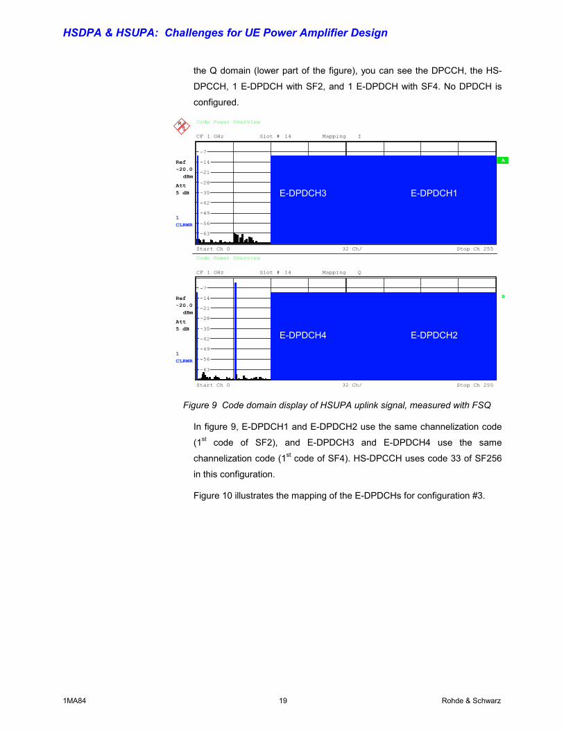
HSDPA & HSUPA: Challenges for UE Power Amplifier Design
1MA84
the Q domain (lower part of the figure), you can see the DPCCH, the HS-
DPCCH, 1 E-DPDCH with SF2, and 1 E-DPDCH with SF4. No DPDCH is
configured.
ARef -20.0
dBm
Ref -20.0
dBm
Ref -20.0
dBm
1CLRWR
Code Power Overview
CF 1 GHz Slot # 14 Mapping I
Ref-20.0
dBm
Ref-20.0
dBm
Ref-20.0
dBm
1CLRWR
Code Power Overview
CF 1 GHz Slot
Att 5 dBAtt 5 dB
Att5 dBAtt5 dB
Start Ch 0
Start Ch 0
-63-56-49-42-35-28-21-14-7
-63-56-49-42-35-28-21-14-7
Figure 9 Code domain
In figure 9, E-DPDC
(1st code of SF2)
channelization code
in this configuration.
Figure 10 illustrates
E-DPDCH3
19
# 14 Mapping Q
32 Ch/
32 Ch/
display of HSUPA uplink signal
H1 and E-DPDCH2 use the sa
, and E-DPDCH3 and E-DP
(1st code of SF4). HS-DPCCH
the mapping of the E-DPDCHs f
E-DPDCH1
B
Stop Ch 255
E-DPDCH4
E-DPDCH2Rohde & Schwarz
Stop Ch 255
, measured with FSQ
me channelization code
DCH4 use the same
uses code 33 of SF256
or configuration #3.
HSDPA & HSUPA: Challenges for UE Power Amplifier Design
1MA84 20 Rohde & Schwarz
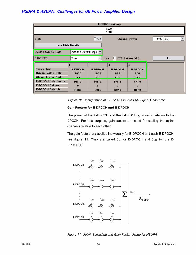
Figure 10 Configuration of 4 E-DPDCHs with SMx Signal Generator
Gain Factors for E-DPCCH and E-DPDCH
The power of the E-DPCCH and the E-DPDCH(s) is set in relation to the
DPCCH. For this purpose, gain factors are used for scaling the uplink
channels relative to each other.
The gain factors are applied individually for E-DPCCH and each E-DPDCH,
see figure 11. They are called βec for E-DPCCH and βed,k for the E-
DPDCH(s).
Figure 11 Uplink Spreading and Gain Factor Usage for HSUPA
Σ I+jQ
Se-dpch
ced,1 βed,1
E-DPDCH1
iqed,1
ced,k βed,k
E-DPDCHk
iqed,k
ced,K βed,K
E-DPDCHK
iqed,K
cec βec
E-DPCCH
iqec
.
.
.
.
.
.
.
.

HSDPA & HSUPA: Challenges for UE Power Amplifier Design
1MA84 21 Rohde & Schwarz
eccec A⋅= ββ
The UE derives these gain factors from higher layer signaling as follows.
Gain Factor for E-DPCCH
E-DPCCH is scaled with a gain factor βec, which is given by:
where βc is the gain factor of the DPCCH. βc is either signaled by higher
layers to the UE, or computed according to [6]. The ratio Aec is derived from
the parameter ∆E-DPCCH signaled by higher layers, e.g. at call setup.
Table 9 shows the meaning of the signaled values for ∆E-DPCCH. The UE
will scale the E-DPCCH in relation to the DPCCH according to the
quantized amplitude ratio.
Table 9 – E-DPCCH power relative to DPCCH
Signaling values for
∆ E-DPCCH
Quantized amplitude ratios
Aec = βec /βc
E-DPCCH power to be set in
relation to DPCCH
8 30/15 6.02
7 24/15 4.08
6 19/15 2.05
5 15/15 0.0
4 12/15 -1.94
3 9/15 -4.44
2 8/15 -5.46
1 6/15 -7.96
0 5/15 -9.54
During compressed frames, the E-DPCCH gain factor βec needs to be
scaled according to [6].
Gain Factor for E-DPDCH
There can be one or more E-DPDCH(s), and each of them is scaled with an
own gain factor, see figure 11. The gain factors may vary on radio frame
basis or sub-frame basis depending on whether the E-DCH TTI is 10 ms or
2 ms, respectively.
The gain factor βed,k for the kth E-DPDCH is determined by the transport
format combination on E-DCH (E-TFC) carried in this TTI, and depending
on the HARQ profile for the data carried in this TTI.

HSDPA & HSUPA: Challenges for UE Power Amplifier Design
1MA84 22 Rohde & Schwarz
Background:
The E-TFC describes the size of the transport block carried in a TTI. This
parameter therefore influences the required transmission power.
For each data flow (MAC-d flow), higher layers can configure an individual HARQ
profile. The HARQ profile includes the power offset and maximum number of
HARQ retransmissions to use for this MAC-d flow. This can be used to fine-tune
operating points for different data flows.
The UE determines the gain factor βed,k based on parameters signaled by
higher layers (e.g. at call setup).
First, a “reference E-TFC” needs to be determined in the UE for the E-TFC
carried in the regarded TTI. A list of reference E-TFCs containing up to 8
reference E-TFCs is signaled by higher layers. The reference E-TFC is
selected as close as possible to the regarded E-TFC [6].
Then, a reference gain factor βed,ref is determined for the selected reference
E-TFC:
where βc is the gain factor of the DPCCH. The ratio Aed is derived from the
parameter ∆E-DPDCH signaled by higher layers for the selected reference
E-TFC. Table 10 shows the meaning of the signaled values for ∆E-DPDCH.
Background:
The reference E-TFC concept is used in order to avoid the signaling overhead
which would result from signaling a ∆E-DPDCH value for all possible E-TFC
values.
edcrefed A⋅= ββ ,

HSDPA & HSUPA: Challenges for UE Power Amplifier Design
1MA84 23 Rohde & Schwarz
Table 10 Quantization for ∆E-DPDCH
However, this reference gain factor cannot directly be used for scaling the
E-DPDCHs, since the reference E-TFC does not reflect the actual E-TFC in
terms of number of data bits contained and number of E-DPDCHs required
for transmission. Furthermore, the HARQ profile needs to be considered.
Therefore, for the E-TFC to be transmitted in the TTI under consideration
(the jth E-TFC), a temporary variable βed,j,harq is computed as:
20, ,, , ,
, ,
10harq
e ref e jed j harq ed ref
e j e ref
L KL K
β β∆
= ⋅
where
Le,ref is the number of E-DPDCHs used for the reference E-TFC
Le,j is the number of E-DPDCHs used for the j:th E-TFC
Ke,ref is the number of data bits of the reference E-TFC
Ke,j is the number of data bits of the j:th E-TFC.
∆harq is the HARQ offset for the specific data flow to be transmitted (so-
called “MAC-d flow”) as signaled by higher layers (see table 11).

HSDPA & HSUPA: Challenges for UE Power Amplifier Design
1MA84 24 Rohde & Schwarz
Table 11 HARQ Offset ∆harq
NOTE: refeL , and jeL , represent “equivalent” number of physical channels.
Normally they are equal to number of used E-DPDCHs except for two
cases:
1. 2 x SF2 case: refeL , and jeL , should be 4 instead of 2.
2. 2 x SF2 + 2 x SF4 case: refeL , and jeL , should be 6 instead of 4.
Therefore, the calculated βed,j,harq must be scaled by a factor of 2 for
SF=2 codes. The unquantized gain factor βed,k,j,uq is set to , ,2 ed j harqβ×
for E-DPDCHs using spreading factor 2 and equal to βed,j,harq otherwise. The
ratio βed,k,j,uq / βc is now quantized according to table 12 to obtain the ratio
βed,k / βc.

HSDPA & HSUPA: Challenges for UE Power Amplifier Design
1MA84 25 Rohde & Schwarz
Table 12 Quantization for βed,k / βc
During compressed frames, the E-DPDCH gain factor βed,k needs to be
scaled according to [6].
UE Transmitter Tests for HSUPA
[12] currently contains the following transmitter tests for HSUPA UEs:
− Test Case 5.2B: Maximum Output Power with HS-DPCCH and E-DCH
− Test Case 5.9B: Spectrum Emission Mask with E-DCH
− Test Case 5.10B: Adjacent Channel Leakage Power Ratio (ACLR) with
E-DCH
Also for HSUPA, the cubic metric is used to determine the maximum power
reduction for different signal characteristics. Thus, table 4 is also valid for
HSUPA.
Uplink Reference Measurement Channel for E-DCH Tests
The reference measurement channel for E-DCH tests describes L1 and L2
parameters to use for the test cases [12]. For transmitter tests, table 13
shows the required beta combinations.

HSDPA & HSUPA: Challenges for UE Power Amplifier Design
1MA84 26 Rohde & Schwarz
Table 13 β values for UE transmitter tests with HS-DPCCH/E-DCH
Sub
-
test
βc βd βd
(SF)
βc/βd βHS
(Note1)
βec βed βed
(SF)
βed
(Code
s)
CM
(dB)
(Note 2)
MPR
(dB)
(Note 2)
1 8/15 15/15 64 8/15 16/15 16/15 448/75 4 1 1.0 0.0
2 6/15 15/15 64 6/15 12/15 12/15 94/75 4 1 3.0 2.0
3 15/15 5/15 64 15/5 30/15 30/15 βed1: 47/15
βed2: 47/15
4
4
2 2.0 1.0
4 1/15 15/15 64 1/15 2/15 2/15 56/75 4 1 3.0 2.0
5 12/15 15/15 64 12/15 24/15 24/15 224/25 4 1 1.0 0.0
Note 1: ∆ACK, ∆NACK and ∆CQI = 30/15 with hsβ = 30/15 * cβ .
Note 2: CM = 1 for βc/βd =12/15, βhs/βc=24/15. For all other combinations of DPDCH, DPCCH, HS- DPCCH, E-
DPDCH and E-DPCCH the MPR is based on the relative CM difference.
4 Basic Test Setups with R&S Instruments
In this chapter, it is explained how to create and analyze HS-DPCCH, E-
DPCCH and E-DPDCH signals for UE power amplifier testing with R&S
instruments.
Generation of HS-DPCCH, E-DPCCH and E-DPDCH
For generating these signals, signal generators SMU200A, SMJ100A or
SMATE200A are available. Software option SMx-K43 (3GPP FDD
enhanced MS/BS tests, incl. HSDPA, requires SMx-K42) provides HSDPA
functionality on these signal generators. Software option SMx-K45 provides
HSUPA functionality (3GPP FDD HSUPA, requires SMx-K42).
Alternatively, WinIQSIM2 simulation software provides the possibility to
generate HS-DPCCH and E-DCH signals. WinIQSIM2 is running on a PC
and can generate waveforms for digitally modulated signals which can be
output by the Arbitrary Waveform Generator AFQ100A as well as the
integrated solutions in the vector signal generators SMU200A and the
SMJ100A.
In the following, SMU200A signal generator is exemplarily used to
demonstrate the test setup for the signal generation.
With the SMU200A, settings for digital modulation can be accessed via the
baseband function block in the block diagram of the user interface. Figure

HSDPA & HSUPA: Challenges for UE Power Amplifier Design
1MA84 27 Rohde & Schwarz
12 shows the 3GPP FDD menu within the baseband function block. An
uplink signal is created. By double-clicking on the selected User Equipment
(UE1 in this example), it is possible to access more detailed settings of the
generated signal including DPCCH, DPDCH, HS-DPCCH, E-DPCCH and
E-DPDCH parameters
Figure 12 – Uplink signal generation with SMU200A
Figure 13 shows the possible HS-DPCCH settings with SMU200A. The
sub-frame structure of the HS-DPCCH is graphically illustrated. Power,
Start Delay, Inter TTI Distance, CQI pattern, and ACK/NACK pattern can be
selected. The parameter Start Delay is corresponding to the parameter m in
figure 5, and is therefore determining the position of the HS-DPCCH
compared to the uplink DPCH frame boundary. Power offsets for ACK and
NACK fields within HS-DPCCH can be set independently in relation to the
HS-DPCCH power. CQI power is then equal to HS-DPCCH power.

HSDPA & HSUPA: Challenges for UE Power Amplifier Design
1MA84 28 Rohde & Schwarz
Figure 13 – HS-DPCCH Settings in SMU200A menu
Figure 14 shows the possible E-DPCCH settings with SMU200A. The sub-
frame structure of the E-DPCCH is graphically illustrated. Power,
Retransmission Sequence Number, E-TFCI Information, E-DCH TTI,
Happy Bit and a DTX Pattern can be selected. Selection of HSUPA Fixed
Reference channels required for BS testing according to 3GPP TS 25.141
[16] can be obtained by the HSUPA FRC button.
Figure 14 – E-DPCCH Settings in SMU200A menu
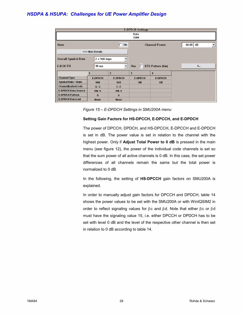
Figure 15 shows the possible E-DPDCH settings with SMU200A. The sub-
frame structure of the E-DPDCH is graphically illustrated. Channel Power,
Symbol Rate, E-DCH TTI, DTX Pattern and adjustments on each of the
four possible data channels can be selected.
HSDPA & HSUPA: Challenges for UE Power Amplifier Design
1MA84 29 Rohde & Schwarz
Figure 15 – E-DPDCH Settings in SMU200A menu
Setting Gain Factors for HS-DPCCH, E-DPCCH, and E-DPDCH
The power of DPCCH, DPDCH, and HS-DPCCH, E-DPCCH and E-DPDCH
is set in dB. The power value is set in relation to the channel with the
highest power. Only if Adjust Total Power to 0 dB is pressed in the main
menu (see figure 12), the power of the individual code channels is set so
that the sum power of all active channels is 0 dB. In this case, the set power
differences of all channels remain the same but the total power is
normalized to 0 dB.
In the following, the setting of HS-DPCCH gain factors on SMU200A is
explained.
In order to manually adjust gain factors for DPCCH and DPDCH, table 14
shows the power values to be set with the SMU200A or with WinIQSIM2 in
order to reflect signaling values for βc and βd. Note that either βc or βd
must have the signaling value 15, i.e. either DPCCH or DPDCH has to be
set with level 0 dB and the level of the respective other channel is then set
in relation to 0 dB according to table 14.

HSDPA & HSUPA: Challenges for UE Power Amplifier Design
1MA84 30 Rohde & Schwarz
Table 14 – Power values to be set on SMU200A for βc and βd values
Signaling values for
βc and βd
Quantized amplitude ratios for
βc and βd
Power to be set for R&S Vector
Signal Generator / dB
15 1.0 0.0
14 14/15 -0.60
13 13/15 -1.24
12 12/15 -1.94
11 11/15 -2.69
10 10/15 -3.52
9 9/15 -4.44
8 8/15 -5.46
7 7/15 -6.62
6 6/15 -7.96
5 5/15 -9.54
4 4/15 -11.48
3 3/15 -13.99
2 2/15 -17.52
1 1/15 -23.52
0 Switch off Switch channel off
In case of additional HS-DPCCH, its levels are set in relation to the DPCCH
according to table 15.
Table 15 – HS-DPCCH power relative to DPCCH
Signaling values for
∆ ACK, ∆NACK and ∆CQI
Quantized amplitude ratios for
∆ −
2010DPCCHHS
HS-DPCCH power to be set in
relation to DPCCH
8 30/15 6.02
7 24/15 4.08
6 19/15 2.05
5 15/15 0.0
4 12/15 -1.94
3 9/15 -4.44
2 8/15 -5.46
1 6/15 -7.96
0 5/15 -9.54

HSDPA & HSUPA: Challenges for UE Power Amplifier Design
1MA84 31 Rohde & Schwarz
It needs to be considered that in the SMU200A and in WinIQSIM2, the level
of the channel with the highest power has to be set to 0 dB. The power of
the other channels is then set in relation to 0 dB. This step is simplified with
the demo software explained below in this chapter.
Setting of gain factors for E-DPCCH works in a similar way. Table 16 shows
the required power values depending on βec.
Table 16 – E-DPCCH power relative to DPCCH
Signaling values for
∆ E-DPCCH
Quantized amplitude ratios
Aec = βec /βc
E-DPCCH power to be set in
relation to DPCCH
8 30/15 6.02
7 24/15 4.08
6 19/15 2.05
5 15/15 0.0
4 12/15 -1.94
3 9/15 -4.44
2 8/15 -5.46
1 6/15 -7.96
0 5/15 -9.54
For E-DPDCH, the principle of setting gain factors is the same as for the
other uplink channels. However, more parameters are influencing the exact
gain factor selection, e.g. transport block size, HARQ profile. Therefore,
table 17 exemplarily shows the power values to set on SMU200A or
WinIQSIM2 in order to reflect the subtests of [12] required for UE
transmitter testing, see table 13 as mentioned above.
Table 17 Power values for uplink channels to be used for transmitter tests
in 3GPP TS 34.121
Subtest
DPCCH
βc
DPDCH
βd
HS-DPCCH
βHS
E-DPCCH
βec
E-DPDCH
βed
1 -20,98dB -15,52dB -14,96dB -14,96dB 0dB
2 -9,92dB -1,96dB -3,9dB -3,9dB 0dB
3 -9,92dB -19,46dB -3,9dB -3,9dB 0dB/0dB
4 -23,52dB 0dB -17,5 dB -17,5 dB -2,54dB
5 -20,98 dB -19,04dB -14,96dB -14,96dB 0dB
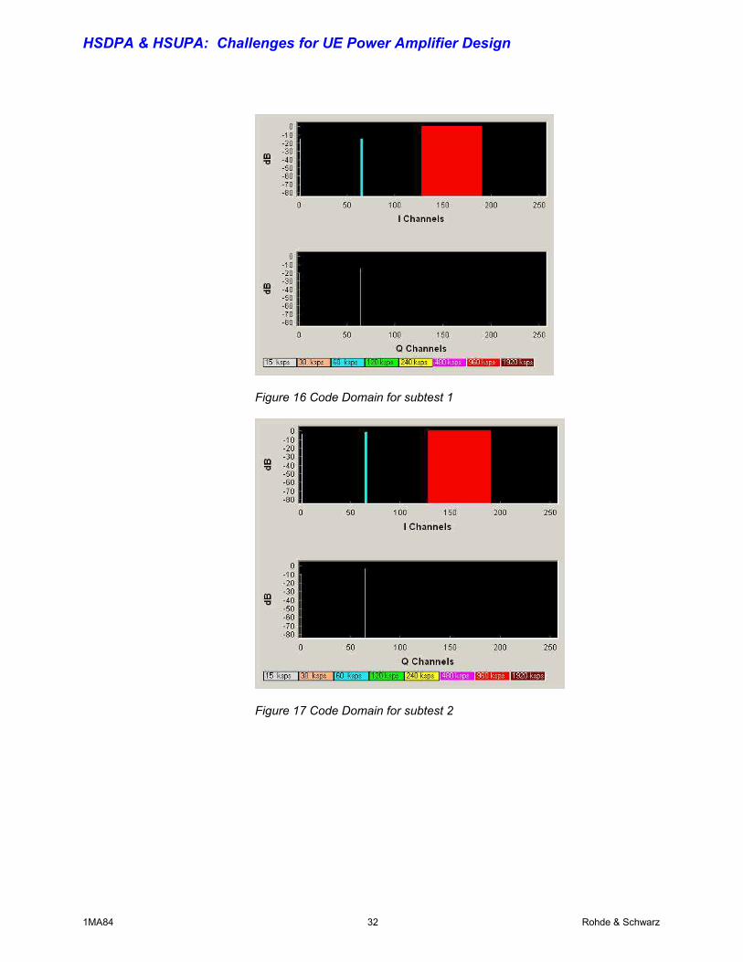
Figures 16-20 show the resulting code domain views for these subtests.
HSDPA & HSUPA: Challenges for UE Power Amplifier Design
1MA84 32 Rohde & Schwarz
Figure 16 Code Domain for subtest 1
Figure 17 Code Domain for subtest 2

HSDPA & HSUPA: Challenges for UE Power Amplifier Design
1MA84 33 Rohde & Schwarz
Figure 18 Code Domain for subtest 3
Figure 19 Code Domain for subtest 4

HSDPA & HSUPA: Challenges for UE Power Amplifier Design
1MA84 34 Rohde & Schwarz
Figure 20 Code Domain for subtest 5
Analysis of HS-DPCCH, E-DPCCH, E-DPDCH with R&S Instruments
For analyzing the RF characteristics of an HS-DPCCH or E-DCH signal,
spectrum analyzers FSU and FSP as well as the signal analyzer FSQ can
be used. Software options FS-K72 (3GPP-FDD BTS transmitter test for
FSMR, FSP, FSU, FSQ), FS-K73 (Application firmware 3GPP-FDD UE
transmitter test for FSMR, FSP, FSU, FSQ) and FS-K74 (3GPP HSDPA
base station test application firmware for FSMR, FSU, FSP, FSQ) provide
HSDPA and HSUPA functionality.
Also the CMU200 Universal Radio Communication Tester provides a
variety of uplink analysis and measurement functions for HSDPA and
HSUPA. Software Options CMU-K64 (Software option for CMU200:
HSDPA) and CMU-K60 (Software option for CMU200: HSDPA 10 Mbps
ext.) enable HSDPA functionality, and software option CMU-K56 (Software
option for CMU200: HSUPA 5.7 Mbps) enables HSUPA functionality.
CMU200 functionality is shown at the end of this chapter.
In the following, FSQ signal analyzer is exemplarily used to demonstrate the
test setup for uplink analysis.
For power amplifier design, particularly ACLR, crest factor, EVM and
spectrum measurements are of interest. These measurements can be
performed conveniently and with highest accuracy with the FSQ.

HSDPA & HSUPA: Challenges for UE Power Amplifier Design
1MA84 35 Rohde & Schwarz
For accessing the ACLR measurement, press the key MEAS, and then the
ACLR softkey. The instrument measures the channel power and the
relative power of adjacent channels and of the next channels. Figure 21
shows an example.
Ref 5 dBm Att 10 dB*
**
1 RMCLRWR
ASGL
RBW 30 kHzVBW 300 kHzSWT 100 ms*
Center 2.12 GHz Span 25.5 MHz2.55 MHz/-90-80-70-60-50-40-30-20-100
Tx Channel W-CDMA 3GPP REV Bandwidth 3.84 MHz Power -2.84 dBm Adjacent Channel
Bandwidth 3.84 MHz Lower -67.84 dB Spacing 5 MHz Upper -69.52 dB Alternate Channel Bandwidth 3.84 MHz Lower -72.34 dB Spacing 10 MHz Upper -72.10 dB
Figure 21 - ACLR measurement with FSQ
In the following you find a short explanation where you can find more
relevant measurements within the FSQ menu:
• Crest factor: via key MEAS, softkey STATISTICS
• Spectrum emission mask: via key MEAS, softkey SPECTRUM EM
MASK
• Composite EVM measurement: via hotkey RESULTS
As further examples, figures 22 and 23 show crest factor measurements on
FSQ with different beta factor combinations. Figure 22 shows the CCDF of
an example reference signal without HS-DPCCH and with gain factors
βc/βd = 8/15. The signal contains 1 DPDCH (channelization code 64 of SF
64). The crest factor of this signal is 3.56 dB. The measurement has been
made with the FSQ.

HSDPA & HSUPA: Challenges for UE Power Amplifier Design
1MA84 36 Rohde & Schwarz
Ref 5 dBm Att 10 dB*
Center 2.12 GHz 2 dB/ Mean Pwr + 20 dB
1 SACLRWR
A
RBW 10 MHz
AQT 62.5 ms
1E-5
1E-4
1E-3
0.01
0.1
Complementary Cumulative Distribution Function
Samples 1000000
Trace 1Mean -2.72 dBmPeak 0.84 dBmCrest 3.56 dB
Figure 22 - Crest factor for βc/βd = 8/15, no HS-DPCCH
For comparison, an HS-DPCCH is added to this signal, and βc/βd/βhs =
15/8/15 is selected. HS-DPCCH is assumed to be time aligned to uplink
DPCCH (parameter start delay = 0), and Inter TTI distance of 3 is selected.
Figure 23 shows the resulting CCDF measured with FSQ. The crest factor
has increased to 6.81 dB.
Ref 5 dBm Att 10 dB*
Center 2.12 GHz 2 dB/ Mean Pwr + 20 dB
1 SACLRWR
A
RBW 10 MHz
AQT 62.5 ms
1E-5
1E-4
1E-3
0.01
0.1
Complementary Cumulative Distribution Function
Samples 1000000
Trace 1Mean -2.80 dBmPeak 4.02 dBmCrest 6.81 dB
Figure 23 - Crest factor for βc/βd/βhs = 15/8/15
Of course, the same measurement types are available for an HSUPA
signal.
The Radio Communication Tester CMU200 offers HS-DPCCH analysis
functionality in signaling and non-signaling mode. In signaling mode,

HSDPA & HSUPA: Challenges for UE Power Amplifier Design
1MA84 37 Rohde & Schwarz
various parameters relevant for HS-DPCCH can be adjusted which are then
signaled by higher layers (RRC – Radio Resource Control) to the UE. The
UE accordingly configures its HS-DPCCH transmission. Figure 24 shows
the menu where gain factors βc, βd and power offsets ∆ACK, ∆NACK and
∆CQI can be set according to the signaling values as given in tables 1 and
2 of this application note.
Figure 24 – Setting of gain factors in CMU200
As explained in chapter 2, the downlink DPCH frame offset (T_dpch_offset
in figure 5) directly influences the timing of the HS-DPCCH in relation to the
uplink DPCH frame boundary. The CMU200 allows to adjust the downlink
DPCH frame offset in multiples of 256 chips which will be signaled by RRC
to the UE. Figure 25 shows the menu for setting this parameter.

HSDPA & HSUPA: Challenges for UE Power Amplifier Design
1MA84 38 Rohde & Schwarz
Figure 25 – Setting of Downlink DPCH frame offset in CMU200
Note that a downlink DPCH frame offset of 0 chips results in an HS-DPCCH
timing of 1 symbol delay (corresponding to 1/10 of a time slot) compared to
the uplink DPCH slot boundary. A downlink DPCH frame offset of 1, 11,
21, …* 256 chips will result in a slot alignment of uplink DPCH and HS-
DPCCH.
Different measurement possibilities exist for the HS-DPCCH, both in
signaling and non-signaling mode. An internal trigger can be generated
upon HS-DPCCH reception which can be used for triggering power,
spectrum, and modulation measurements. Individual trigger offsets can be
adjusted. Figure 26 shows a modified code domain display which allows to
estimate power levels of DPCCH, DPDCH and HS-DPCCH, as well as a
representation of the power of the 10 symbols contained in one HS-DPCCH
time slot. The measurement is done over one uplink DPCH time slot.

HSDPA & HSUPA: Challenges for UE Power Amplifier Design
1MA84 39 Rohde & Schwarz
Figure 26 – Analysis of HS-DPCCH power (per symbol over a
measurement interval of 1 UL DPCH time slot); HS-DPCCH with
ACK/NACK and CQI
In the measurement in figure 26, HS-DPCCH is not slot aligned with uplink
DPCH. The downlink DPCH frame offset is set to 0, so the HS-DPCCH
time slot starts one symbol later than the uplink DPCH slot. The HS-
DPCCH sub-frame in this example contains ACK/NACK and CQI values.
Since different power values for ∆ACK, ∆NACK and ∆CQI have been set,
one can see a power step within the measured slot. Figure 27 illustrates the
measurement principle
Figure 27 – HS-DPCCH slot timing not aligned with uplink DPCH slot timing
UL DPCH time slot = measurement interval
HS-DPCCH time slot carrying
CQI
HS-DPCCH time slot carrying
ACK/NACK
HS-DPCCH time slot carrying
CQI Power level
determined by ∆ACK / ∆NACK
Power level determined by
∆CQI
Power level determined by
∆CQI

HSDPA & HSUPA: Challenges for UE Power Amplifier Design
1MA84 40 Rohde & Schwarz
As another example, in figure 28, an HS-DPCCH sub-frame without an
ACK/NACK field (DTX) has been measured.
Figure 28 – Analysis of HS-DPCCH power (per symbol over a
measurement interval of 1 UL DPCH time slot), no ACK/NACK field
The timing of the HS-DPCCH and the measurement interval is still as in
figure 26, but this time, the ACK/NACK field of HS-DPCCH is blanked.
Figure 29 shows an EVM measurement of a signal containing HS-DPCCH.
Figure 29 – EVM Measurement of a signal containing HS-DPCCH

HSDPA & HSUPA: Challenges for UE Power Amplifier Design
1MA84 41 Rohde & Schwarz
Figure 30 shows the code domain analysis on CMU200 for a signal
containing E-DPDCHs and E-DPCCH, and figure 31 shows the modified
code domain view indicating the measured power values of all uplink
channels separately.
Figure 30 – Code domain view of HSUPA signal on CMU200
Figure 31 Manual code domain view of HSUPA signal on CMU200

HSDPA & HSUPA: Challenges for UE Power Amplifier Design
1MA84 42 Rohde & Schwarz
Demo Software for HSDPA measurements
This application note comes with a small demo program called “GDE”
(Generic Demonstration Engine). The software is running on a PC. For
installing it, download and start the file 1MA84_1.0.exe which will guide you
through the installation process.
The GDE is a remote control command sequencer tool. It offers a user
interface for setting basic parameters of an HSDPA signal with DPCCH,
DPDCH, and HS-DPCCH, and for measuring ACLR, crest factor, or
composite EVM of this signal. After selecting the measurement of interest
and configuring the parameters, R&S instruments like SMU200A and FSQ
are preconfigured via remote control, and the measurement is done
automatically. Figure 32 shows the user interface of the GDE.
Within the Help menu (Help for GDE general), a detailed explanation of the
software can be found.
You can select from crest factor measurement, ACLR measurement, or
composite EVM measurement (1). For editing the test setup, select (2). A
test editor as shown in figure 33 opens up.

HSDPA & HSUPA: Challenges for UE Power Amplifier Design
1MA84 43 Rohde & Schwarz
Figure 32 - User Interface of GDE, Crest Factor measurement selected
The text editor allows to input values for βc, βd and βhs (called bc, bd and
bhs in this program), which are then automatically converted to the correct
level setting in the SMU200A. Note that for simplicity all beta factors are
assumed to be relative to the amplitude factor 1/15 in this user interface.
This also reflects the gain factor settings requested for the test cases in
[12]. However, for correctly determining the values, you have to be aware
that the beta factor of HS-DPCCH is defined relative to the beta factor of
DPCCH, see table 15. In case of no HS-DPCCH or no DPDCH signal,
insert bhs = 0 or bd = 0, respectively.
12
3
4
5

HSDPA & HSUPA: Challenges for UE Power Amplifier Design
1MA84 44 Rohde & Schwarz
Figure 33 - Editing a test setup with the GDE
Besides beta factors, also inter TTI distance, start delay, and DPDCH
symbol rate can be set. The DPDCH symbol rate can be conveniently
selected in a list (figure 34).
Figure 34 - User Selection of DPDCH symbol rate
The test setup file can easily be customized to enable more settings, based
on the remote control commands for SMU200A and FSQ.
Setting of βc, βd
Setting of βhs

HSDPA & HSUPA: Challenges for UE Power Amplifier Design
1MA84 45 Rohde & Schwarz
When you have saved your settings, reload the test setup ((3) in figure 32),
pre-configure the instruments and do the measurement ((4) in figure 32).
The relevant test case parameters are displayed in the user interface ((5) in
figure 32).
5 Abbreviations
3GPP 3rd Generation Partnership Project
ACK Acknowledgement
ACLR Adjacent Channel Leakage Ratio
AMR Adaptive Multirate Codec
ARQ Automatic Repeat Request
BLER Block Error Rate
CCDF Complementary Cumulative Distribution Function
CM Cubic Metric
CQI Channel Quality Indicator
DPCCH Dedicated Physical Control Channel
DPCH Dedicated Physical Channel
DPDCH Dedicated Physical Data Channel
DTX Discontinuous Transmission
DUT Device under Test
E-DCH Enhanced Dedicated Channel
E-DPCCH E-DCH Dedicated Physical Control Channel
E-DPDCH E-DCH Dedicated Physical Data Channel
E-TFCI E-DCH Transport Format Combination Indicator
EUL Enhanced Uplink
EVM Error Vector Magnitude
FDD Frequency Division Duplex
HARQ Hybrid Automatic Repeat Request
HSDPA High Speed Downlink Packet Access

HSDPA & HSUPA: Challenges for UE Power Amplifier Design
1MA84 46 Rohde & Schwarz
HS-DSCH High Speed Downlink Shared Channel
HS-DPCCH High Speed Dedicated Physical Control Channel
HS-PDSCH High Speed Physical Downlink Shared Channel
HS-SCCH High Speed Shared Control Channel
HSUPA High Speed Uplink Packet Access
MAC Medium Access Control
MPR Maximum Power Reduction
NACK Negative Acknowledgement
NAS Non-Access Stratum
PAR Peak-to-Average Ratio
P-CCPCH Primary Common Control Physical Channel
PHY Physical Layer
PO Power Offset
QPSK Quadrature Phase Shift Keying
PDU Protocol Data Unit
RLC Radio Link Control
RRC Radio Resource Control
RSN Retransmission Sequence Number
RV Redundancy Version
SF Spreading Factor
SG Serving Grant
TFC Transport Format Combination
TFCI Transport Format Combination Indicator
TS Technical Specification
TTI Transmission Time Interval
UE User Equipment
UMTS Universal Mobile Telecommunications System
WCDMA Wideband Code Division Multiple Access

HSDPA & HSUPA: Challenges for UE Power Amplifier Design
1MA84 47 Rohde & Schwarz
6 Additional Information
This application note is updated from time to time. Please visit the website
1MA84 in order to download new versions.
Please contact [email protected] for comments
and further suggestions.
7 References
[1] Application Note 1MA82; HSDPA Test and Measurement
Requirements, Rohde & Schwarz
[2] Application Note 1MA94; High Speed Uplink Packet Access (HSUPA)
White Paper, Rohde & Schwarz
[3] 3GPP TS 25.211; Physical channels and mapping of transport channels
onto physical channels (FDD) (Release 6)
[4] 3GPP TS 25.212; Multiplexing and Channel Coding (FDD) (Release 6)
[5] 3GPP TS 25.213; Spreading and Modulation (FDD) (Release 6)
[6] 3GPP TS 25.214; Physical layer procedures (FDD) (Release 6)
[7] 3GPP TS 25.101; User Equipment Radio Transmission and Reception
(FDD) (Release 5)
[8] 3GPP TS 25.101; User Equipment Radio Transmission and Reception
(FDD) (Release 6)
[9] R4-030796; ACLR Requirements under HSDPA Operation, SEMC
[10] RP-040113; UE maximum power reduction when HS-DPCCH is
transmitted, Nokia
[11] R4- 040102; HSDPA PA Back-off, Motorola
[12] 3GPP TS 34.121; Terminal conformance specification ; Radio
transmission / reception (FDD) (Release 7)
[13] R4- 040367; Comparison of PAR and Cubic Metric for Power De-
rating, Motorola
[14] R4-040721; Mapping of cubic metric to additional PA headroom,
Qualcomm

HSDPA & HSUPA: Challenges for UE Power Amplifier Design
1MA84 48 Rohde & Schwarz
[15] 3GPP TS 25.321; Medium Access Control (MAC) protocol specification
(Release 6)
[16] 3GPP TS 25.141; Base Station (BS) conformance testing (FDD)
(Release 6)
8 Ordering information
Vector Signal Generator
R&S® SMU200A 1141.2005.02
R&S® SMU-B102 Frequency range 100 KHz to 2.2GHz for
1st RF Path
1141.8503.02
R&S® SMU-B103 Frequency range 100 KHz to 3GHz for
1st RF Path
1141.8603.02
R&S® SMU-B104 Frequency range 100 KHz to 4GHz for
1st RF Path
1141.8703.02
R&S® SMU-B106 Frequency range 100 KHz to 6 GHz for
1st RF Path
1141.8803.02
R&S® SMU-B202 Frequency range 100 KHz to 2.2 GHz for
2nd RF Path
1141.9400.02
R&S® SMU-B203 Frequency range 100 KHz to 3 GHz for
2nd RF Path
1141.9500.02
R&S® SMU-B9 Baseband Generator with digital modulation
(realtime) and ARB (128 M Samples)
1161.0766.02
R&S® SMU-B10 Baseband Generator with digital modulation
(realtime) and ARB (64MSamples)
1141.7007.02
R&S® SMU-B11 Baseband Generator with digital modulation
(realtime) and ARB (16MSamples)
1159.8411.02
R&S® SMU-B13 Baseband Main Module 1141.8003.02
R&S® SMU-K42 Digital Standard 3GPP FDD 1160.7909.02
R&S® SMU-K43 3GPP FDD enhanced MS/BS Tests incl. HSDPA 1160.9660.02
R&S® SMU-K45 3GPP FDD HSUPA 1161.0666.02
R&S® SMU-K242 3GPP FDD for WinIQSIM2 1408.5618.02
R&S® SMU-K243 3GPP FDD enhanced MS/BS tests incl. HSDPA for
WinIQSIM2
1408.5718.02
R&S® SMU-K245 Digital standard HSUPA for WinIQSIM2 1408.5918.02
R&S® SMJ100A 1403.4507.02
R&S® SMJ-B103 Frequency range 100 kHz - 3 GHz 1403.8502.02
R&S® SMJ-B106 Frequency range 100 kHz - 6 GHz 1403.8702.02
R&S® SMJ-B9 Baseband generator with digital modulation
(realtime) and ARB (128 M Samples)
1404.1501.02

HSDPA & HSUPA: Challenges for UE Power Amplifier Design
1MA84 49 Rohde & Schwarz
R&S® SMJ-B10 Baseband Generator with digital modulation
(realtime) and ARB (64MSamples)
1403.8902.02
R&S® SMJ-B11 Baseband Generator with digital modulation
(realtime) and ARB (16MSamples)
1403.9009.02
R&S® SMJ-B13 Baseband Main Module 1403.9109.02
R&S® SMJ-K42 Digital Standard 3GPP FDD 1404.0405.02
R&S® SMJ-K43 3GPP FDD Enhanced MS/BS Tests incl. HSDPA 1404.0505.02
R&S® SMJ-K45 3GPP FDD HSUPA 1409.1816.02
R&S® SMJ-K242 Digital standard 3GPP FDD for WinIQSIM2 1409.0610.02
R&S® SMJ-K243 3GPP FDD enhanced MS/BS Tests incl. HSDPA for
WinIQSIM2
1409.0710.02
R&S® SMJ-K245 Digital standard HSUPA 1409.0910.02
R&S® SMATE200A 1400.7005.02
R&S® SMATE-B103 Frequency range 100 KHz to 3 GHz for
1st RF Path
1401.1000.02
R&S® SMATE-B106 Frequency range 100 KHz to 6 GHz for
1st RF Path
1401.1200.02
R&S® SMATE-B203 Frequency range 100 KHz to 3 GHz for
2nd RF Path
1401.1400.02
R&S® SMATE-B206 Frequency range 100 kHz - 6 GHz for
2nd RF path
1401.1600.02
R&S® SMATE-B10 Baseband Generator with digital modulation
(realtime) and ARB (64MSamples)
1401.2707.02
R&S® SMATE-B11 Baseband Generator with digital modulation
(realtime) and ARB (16MSamples)
1401.2807.02
R&S® SMATE-B13 Baseband Main Module 1401.2907.02
R&S® SMATE-K42 Digital Standard 3GPP FDD 1404.5207.02
R&S® SMATE-K43 3GPP FDD Enhanced MS/BS Tests incl. HSDPA 1404.5307.02
R&S® SMATE-K45 3GPP FDD HSUPA 1404.7300.02
Signal Analyzers, Spectrum Analyzers and Options
R&S® FSP3 9 kHz to 3 GHz 1164.4391.03
R&S® FSP7 9 kHz to 7 GHz 1164.4391.07
R&S® FSP13 9 kHz to 13 GHz 1164.4391.13
R&S® FSP30 9 kHz to 30 GHz 1164.4391.30
R&S® FSP40 9 kHz to 40 GHz 1164.4391.40
R&S® FSQ3 20 Hz to 3.6 GHz 1155.5001.03
R&S® FSQ8 20 Hz to 8 GHz 1155.5001.08
R&S® FSQ26 20 Hz to 26,5 GHz 1155.5001.26
R&S® FSQ40 20 Hz to 40 GHz 1155.5001.40
R&S® FSU3 20 Hz to 3.6 GHz 1166.1660.03
R&S® FSU8 20 Hz to 8 GHz 1166.1660.08
R&S® FSU26 20 Hz to 26.5 GHz 1166.1660.26
R&S® FSU46 20 Hz to 46 GHz 1166.1660.46
R&S® FSU50 20 Hz to 50 GHz 1166.1660.50

HSDPA & HSUPA: Challenges for UE Power Amplifier Design
1MA84 50 Rohde & Schwarz
R&S® FS-K73 Application Firmware 3GPP-FDD UE Transmitter
Test for FSMR, FSP, FSU, FSQ
1154.7252.02
Universal Radio Communication Tester (UE)
R&S® CMU200 1100.0008.02
R&S®CMU-B68var02 HW-option for CMU200
layer 1-board (3GPP/FDD, DL+UL)
1149.9809.02
R&S®CMU-B21var54 HW-option for CMU200/300:
(GSM/GPRS/EDGE)
1100.5200.54
R&S® CMU-B56 HW-option for CMU200: WCDMA and data E2E
for CMU-B21/var. 14
1150.1850.14
R&S® CMU-PK60 Software option for CMU200:
WCDMA-Sig.: 3GPP/FDD/UE, TX-test
generator, band 1-9
1159.3355.04
R&S® CMU-K64 SW-option for CMU200: HSDPA 3GPP 1157.3970.02
R&S® CMU-K60 SW option for CMU200: HSDPA 10Mbps ext. 1200.8200.02
R&S® CMU-K56 SW option for CMU200: HSUPA 5.7Mbps 1200.7803.02
ROHDE & SCHWARZ GmbH & Co. KG . Mühldorfstraße 15 . D-81671 München . P.O.B 80 14 69 . D-81614 München .
Telephone +49 89 4129 -0 . Fax +49 89 4129 - 13777 . Internet: http://www.rohde-schwarz.com
This application note and the supplied programs may only be used subject to the conditions of use set forth in the
download area of the Rohde & Schwarz website.