how to design an antenna for dynamic nfc · pdf filehow to design an antenna for dynamic nfc...
TRANSCRIPT

January 2017 DocID15629 Rev 7 1/27
1
AN2972Application note
How to design an antenna for dynamic NFC tags
Introduction
The dynamic NFC (near field communication) tag devices manufactured by ST feature an EEPROM that can be accessed either through a low-power I2C interface or an RF contactless interface operating at 13.56 MHz. Both short-range (ISO/IEC 14443 Type A) and long-range (ISO/IEC 15693) standard are supported.
Figure 1. Dynamic NFC tags
Dynamic NFC tag can be used in many applications, with the requirement that the processor features an I2C interface.
This application note intends to:
• Explain the basic principle of passive RFID
• Describe the basics of a 13.56 MHz inductive antenna design
• Provide guidelines for a successful integration, from design to production
Table 1 lists the products concerned by this application note.
Table 1. Applicable products
Type Applicable products
Dynamic NFC Tags M24LR, M24SR and ST25DV series Dynamic NFC Tags
www.st.com
Contents AN2972
2/27 DocID15629 Rev 7
Contents
1 Operating mode . . . . . . . . . . . . . . . . . . . . . . . . . . . . . . . . . . . . . . . . . . . . . 5
2 Basic principles and equations . . . . . . . . . . . . . . . . . . . . . . . . . . . . . . . . 6
2.1 Passive RFID technology . . . . . . . . . . . . . . . . . . . . . . . . . . . . . . . . . . . . . . 6
2.2 Simplified equivalent inlay circuit . . . . . . . . . . . . . . . . . . . . . . . . . . . . . . . . 9
2.3 Basic equations . . . . . . . . . . . . . . . . . . . . . . . . . . . . . . . . . . . . . . . . . . . . 10
2.4 Optimum antenna tuning . . . . . . . . . . . . . . . . . . . . . . . . . . . . . . . . . . . . . .11
3 How to design an antenna on a PCB . . . . . . . . . . . . . . . . . . . . . . . . . . . 12
3.1 Inductance of a circular antenna . . . . . . . . . . . . . . . . . . . . . . . . . . . . . . . 12
3.2 Inductance of a spiral antenna . . . . . . . . . . . . . . . . . . . . . . . . . . . . . . . . . 12
3.3 Inductance of a square antenna . . . . . . . . . . . . . . . . . . . . . . . . . . . . . . . . 13
3.4 eDesignSuite antenna design tool . . . . . . . . . . . . . . . . . . . . . . . . . . . . . . 13
3.5 PCB layout . . . . . . . . . . . . . . . . . . . . . . . . . . . . . . . . . . . . . . . . . . . . . . . . 15
3.5.1 Length of the connections between dynamic NFC tag chip and antenna . . . . . . . . . . . . . . . . . . . . . . . . . . . . . . . . . . . . . . . . . . . . . . 15
3.5.2 Ground, power, and signal layers . . . . . . . . . . . . . . . . . . . . . . . . . . . . . 15
3.5.3 Metal surfaces . . . . . . . . . . . . . . . . . . . . . . . . . . . . . . . . . . . . . . . . . . . . 17
4 How to check the NFC/RFID dynamic NFC tag antenna tuning . . . . . . . . . . . . . . . . . . . . . . . . . . . . . . . . . . . . . . . . . . . . . 18
4.1 Antenna tuning measurements with a network analyzer . . . . . . . . . . . . . 18
4.2 Antenna measurements with standard laboratory tools . . . . . . . . . . . . . . 19
5 From design to production . . . . . . . . . . . . . . . . . . . . . . . . . . . . . . . . . . . 22
6 Revision history . . . . . . . . . . . . . . . . . . . . . . . . . . . . . . . . . . . . . . . . . . . 25

DocID15629 Rev 7 3/27
AN2972 List of tables
3
List of tables
Table 1. Applicable products . . . . . . . . . . . . . . . . . . . . . . . . . . . . . . . . . . . . . . . . . . . . . . . . . . . . . . . 1Table 2. K1 and K2 values according to layout . . . . . . . . . . . . . . . . . . . . . . . . . . . . . . . . . . . . . . . . 13Table 3. Frequency compensation examples . . . . . . . . . . . . . . . . . . . . . . . . . . . . . . . . . . . . . . . . . . 17Table 4. Document revision history . . . . . . . . . . . . . . . . . . . . . . . . . . . . . . . . . . . . . . . . . . . . . . . . . 25
List of figures AN2972
4/27 DocID15629 Rev 7
List of figures
Figure 1. Dynamic NFC tags . . . . . . . . . . . . . . . . . . . . . . . . . . . . . . . . . . . . . . . . . . . . . . . . . . . . . . . . 1Figure 2. Dynamic NFC tag operating mode . . . . . . . . . . . . . . . . . . . . . . . . . . . . . . . . . . . . . . . . . . . . 5Figure 3. Dynamic NFC tag chip power mechanism in RF mode . . . . . . . . . . . . . . . . . . . . . . . . . . . . 7Figure 4. Power transfer versus reader/dynamic NFC tag orientation . . . . . . . . . . . . . . . . . . . . . . . . . 7Figure 5. Communication from the reader to the tag . . . . . . . . . . . . . . . . . . . . . . . . . . . . . . . . . . . . . . 8Figure 6. Communication from tag to the reader . . . . . . . . . . . . . . . . . . . . . . . . . . . . . . . . . . . . . . . . . 8Figure 7. Equivalent circuit of the dynamic NFC tag chip and its antenna. . . . . . . . . . . . . . . . . . . . . . 9Figure 8. Equivalent circuit of the dynamic NFC tag chip mounted on a loop antenna . . . . . . . . . . . 10Figure 9. Tuning the dynamic NFC tag antenna . . . . . . . . . . . . . . . . . . . . . . . . . . . . . . . . . . . . . . . . 11Figure 10. Spiral antenna. . . . . . . . . . . . . . . . . . . . . . . . . . . . . . . . . . . . . . . . . . . . . . . . . . . . . . . . . . . 12Figure 11. Square antennas . . . . . . . . . . . . . . . . . . . . . . . . . . . . . . . . . . . . . . . . . . . . . . . . . . . . . . . . 13Figure 12. Antenna user interface screen design module of eDesignsuite . . . . . . . . . . . . . . . . . . . . . 14Figure 13. Correct PCB layout . . . . . . . . . . . . . . . . . . . . . . . . . . . . . . . . . . . . . . . . . . . . . . . . . . . . . . . 15Figure 14. Bad implementation - Example 1 . . . . . . . . . . . . . . . . . . . . . . . . . . . . . . . . . . . . . . . . . . . . 15Figure 15. Bad implementation example No.2 . . . . . . . . . . . . . . . . . . . . . . . . . . . . . . . . . . . . . . . . . . . 16Figure 16. Not recommended implementation. . . . . . . . . . . . . . . . . . . . . . . . . . . . . . . . . . . . . . . . . . . 16Figure 17. Acceptable implementation. . . . . . . . . . . . . . . . . . . . . . . . . . . . . . . . . . . . . . . . . . . . . . . . . 16Figure 18. Effect of metal surfaces on the antenna frequency tuning . . . . . . . . . . . . . . . . . . . . . . . . . 17Figure 19. Measurement equipment . . . . . . . . . . . . . . . . . . . . . . . . . . . . . . . . . . . . . . . . . . . . . . . . . . 18Figure 20. Example of the resonant frequency response of a prototype antenna . . . . . . . . . . . . . . . . 19Figure 21. ISO standard loop antenna. . . . . . . . . . . . . . . . . . . . . . . . . . . . . . . . . . . . . . . . . . . . . . . . . 20Figure 22. Setting up the standard laboratory equipment . . . . . . . . . . . . . . . . . . . . . . . . . . . . . . . . . . 20Figure 23. Example of a frequency response measurement of a prototype antenna . . . . . . . . . . . . . 21Figure 24. Application examples . . . . . . . . . . . . . . . . . . . . . . . . . . . . . . . . . . . . . . . . . . . . . . . . . . . . . 22Figure 25. Detuning effect . . . . . . . . . . . . . . . . . . . . . . . . . . . . . . . . . . . . . . . . . . . . . . . . . . . . . . . . . . 23Figure 26. Impact of housing/packaging material on RF communication . . . . . . . . . . . . . . . . . . . . . . 24
DocID15629 Rev 7 5/27
AN2972 Operating mode
26
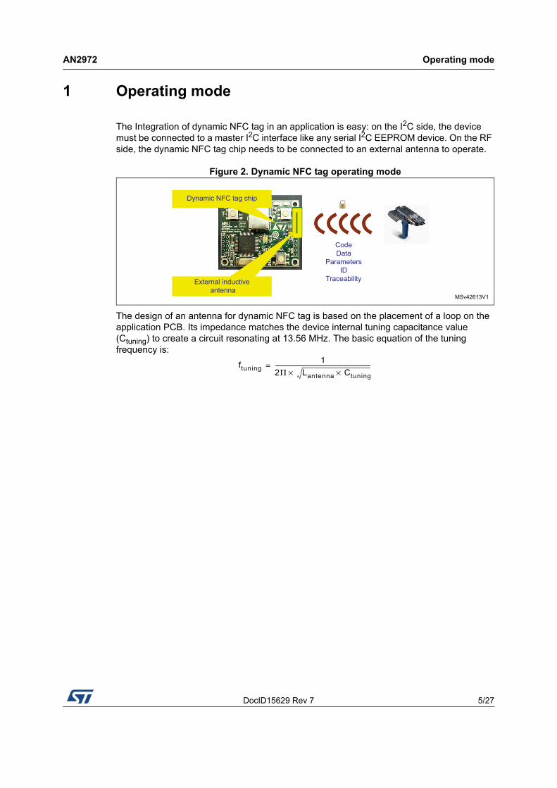
1 Operating mode
The Integration of dynamic NFC tag in an application is easy: on the I2C side, the device must be connected to a master I2C interface like any serial I2C EEPROM device. On the RF side, the dynamic NFC tag chip needs to be connected to an external antenna to operate.
Figure 2. Dynamic NFC tag operating mode
The design of an antenna for dynamic NFC tag is based on the placement of a loop on the application PCB. Its impedance matches the device internal tuning capacitance value (Ctuning) to create a circuit resonating at 13.56 MHz. The basic equation of the tuning frequency is:
ftuning1
2Π Lantenna Ctuning××--------------------------------------------------------------------=
Basic principles and equations AN2972
6/27 DocID15629 Rev 7
2 Basic principles and equations
Definition
• Tag In this document tag denotes the dynamic NFC tag chip mounted on application PCB and connected to its antenna.
• Reader In this document reader denotes an electronic device able to communicate with tags in RF mode.
2.1 Passive RFID technology
The ISO 15693 and ISO 14443 RF protocols used by dynamic NFC tag devices manufactured by ST are based on passive RFID technology, operating in high frequency (HF) range, at 13.56 MHz.
Power transfer
When the dynamic NFC tag chip operates in RF mode, it is powered by the reader. No battery is required to access it in RF mode, neither in read nor in write mode. The dynamic NFC tag chip draws all needed power to operate from the magnetic field generated by the reader through its loop antenna.
The reader - tag system is similar to a voltage transformer where the reader acts as the primary winding, and the tag as the secondary winding.
Reader and tag are magnetically and mutually coupled to each other.
The energy transfer from the reader to the dynamic NFC tag chip depends on:
• How well the tag antenna is tuned close to the reader's carrier frequency (13.56 MHz)
• The distance between the reader and the tag antenna board
• The dimensions of the reader antenna and of the tag antenna board
• The reader power
• The tag antenna orientation related to the reader antenna
DocID15629 Rev 7 7/27
AN2972 Basic principles and equations
26
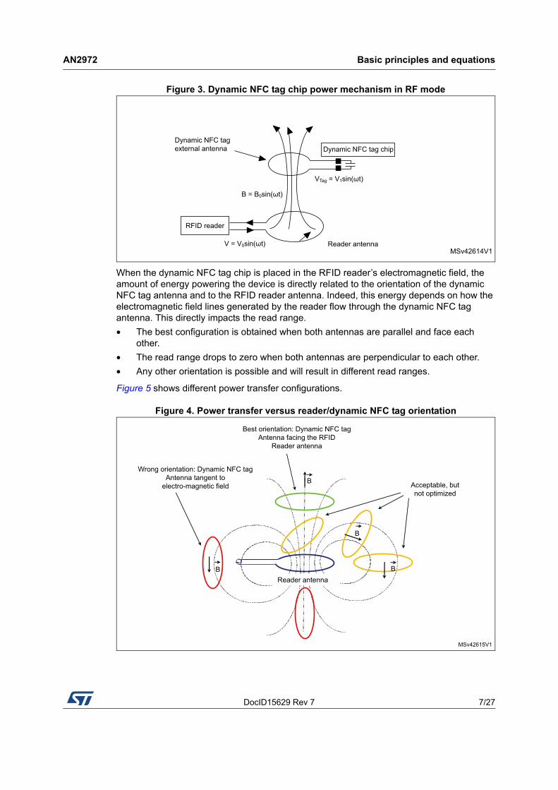
Figure 3. Dynamic NFC tag chip power mechanism in RF mode
When the dynamic NFC tag chip is placed in the RFID reader’s electromagnetic field, the amount of energy powering the device is directly related to the orientation of the dynamic NFC tag antenna and to the RFID reader antenna. Indeed, this energy depends on how the electromagnetic field lines generated by the reader flow through the dynamic NFC tag antenna. This directly impacts the read range.
• The best configuration is obtained when both antennas are parallel and face each other.
• The read range drops to zero when both antennas are perpendicular to each other.
• Any other orientation is possible and will result in different read ranges.
Figure 5 shows different power transfer configurations.
Figure 4. Power transfer versus reader/dynamic NFC tag orientation

Basic principles and equations AN2972
8/27 DocID15629 Rev 7
Data transfer
When placed in a reader’s magnetic field able to power it, the dynamic NFC tag chip built-in circuitry demodulates the information coming from the reader.
Figure 5. Communication from the reader to the tag
At the end of the request, the reader keeps the magnetic field non modulated to power the tag, and allows it to generate an answer. In order to send its response back to the reader, the dynamic NFC tag chip backscatters the data to the reader by internally modulating its input impedance. Tag chip input impedance variation modulates the signal across the reader antenna due to the mutual coupling between reader and tag antennas. Reader electronics demodulates this signal and decodes the tag answer.
Figure 6. Communication from tag to the reader
All this is part of the standard protocol and is taken into account by the dynamic NFC tag chip embedded circuitry and by the RFID reader’s electronics.
DocID15629 Rev 7 9/27
AN2972 Basic principles and equations
26
2.2 Simplified equivalent inlay circuit
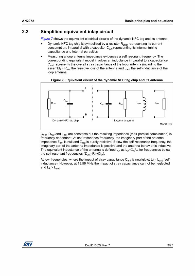
Figure 7 shows the equivalent electrical circuits of the dynamic NFC tag and its antenna.
• Dynamic NFC tag chip is symbolized by a resistor Rchip representing its current consumption, in parallel with a capacitor Ctun representing its internal tuning capacitance and internal parasitics.
• Measuring a loop antenna impedance evidences a self resonant frequency. The corresponding equivalent model involves an inductance in parallel to a capacitance. Cant represents the overall stray capacitance of the loop antenna (including the assembly), Rant the resistive loss of the antenna and Lant the self-inductance of the loop antenna.
Figure 7. Equivalent circuit of the dynamic NFC tag chip and its antenna
Cant, Rant and Lant are constants but the resulting impedance (their parallel combination) is frequency dependent. At self-resonance frequency, the imaginary part of the antenna impedance Zant is null and Zant is purely resistive. Below the self-resonance frequency, the imaginary part of the antenna impedance is positive and the antenna behavior is inductive. The equivalent inductance of the antenna is defined LA as LA=XA/ω for frequencies below the self resonant frequencies (Zant=RA+jXA).
At low frequencies, where the impact of stray capacitance Cant is negligible, LA= Lant (self inductance). However, at 13.56 MHz the impact of stray capacitance cannot be neglected and LA > Lant.
Basic principles and equations AN2972
10/27 DocID15629 Rev 7
2.3 Basic equations
Resonant frequency
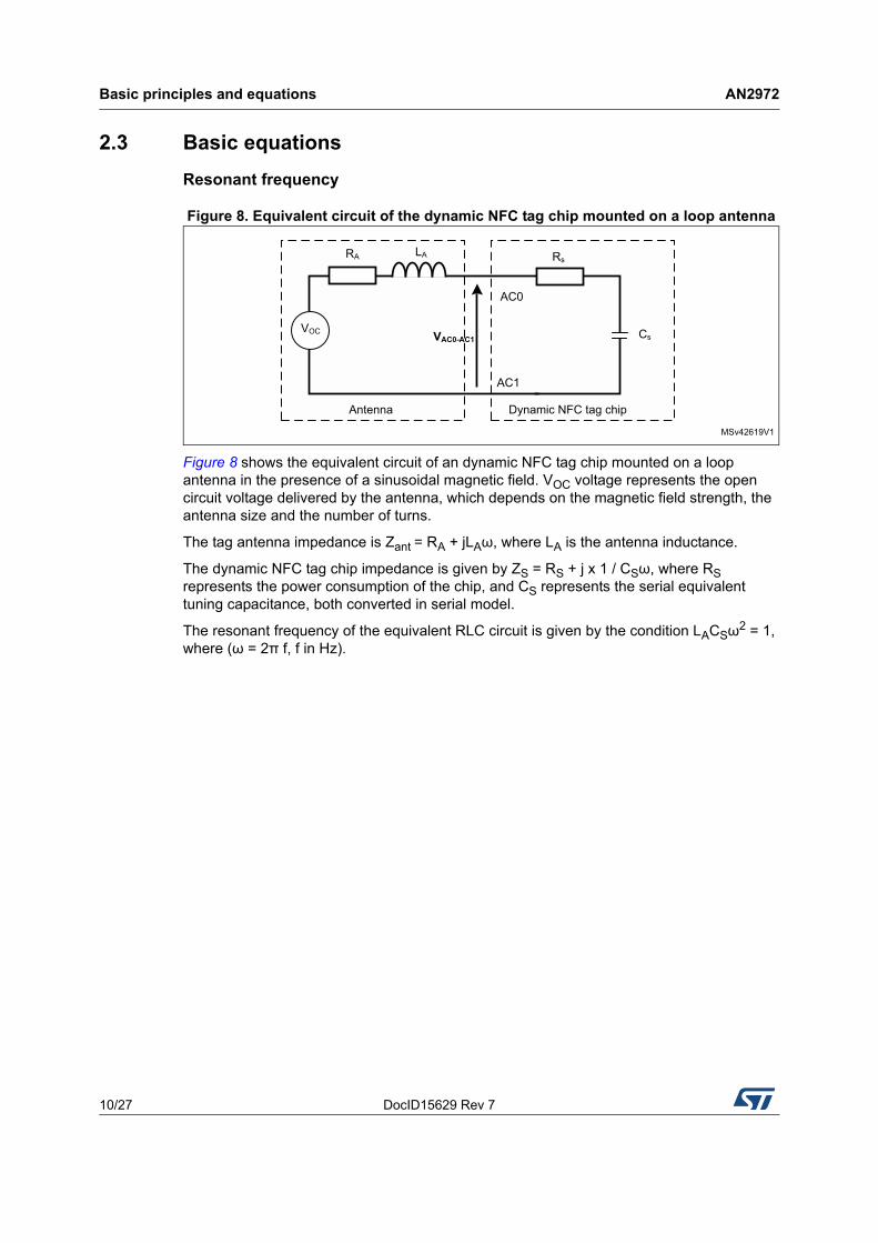
Figure 8. Equivalent circuit of the dynamic NFC tag chip mounted on a loop antenna
Figure 8 shows the equivalent circuit of an dynamic NFC tag chip mounted on a loop antenna in the presence of a sinusoidal magnetic field. VOC voltage represents the open circuit voltage delivered by the antenna, which depends on the magnetic field strength, the antenna size and the number of turns.
The tag antenna impedance is Zant = RA + jLAω, where LA is the antenna inductance.
The dynamic NFC tag chip impedance is given by ZS = RS + j x 1 / CSω, where RS represents the power consumption of the chip, and CS represents the serial equivalent tuning capacitance, both converted in serial model.
The resonant frequency of the equivalent RLC circuit is given by the condition LACSω2 = 1,
where (ω = 2π f, f in Hz).
DocID15629 Rev 7 11/27
AN2972 Basic principles and equations
26
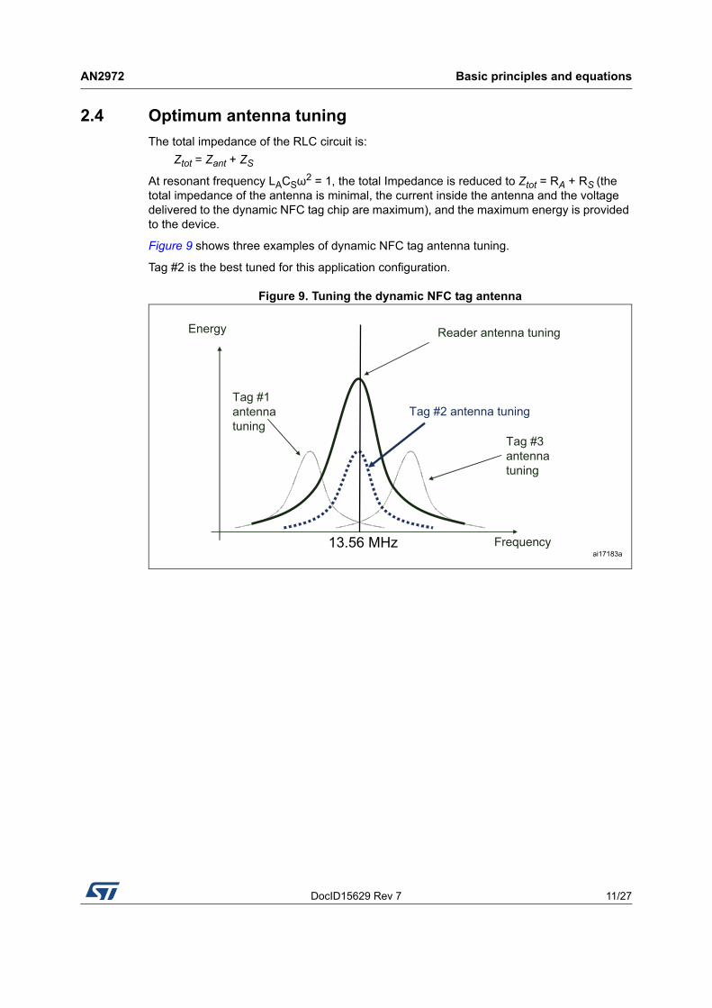
2.4 Optimum antenna tuning
The total impedance of the RLC circuit is:
Ztot = Zant + ZS
At resonant frequency LACSω2 = 1, the total Impedance is reduced to Ztot = RA + RS (the
total impedance of the antenna is minimal, the current inside the antenna and the voltage delivered to the dynamic NFC tag chip are maximum), and the maximum energy is provided to the device.
Figure 9 shows three examples of dynamic NFC tag antenna tuning.
Tag #2 is the best tuned for this application configuration.
Figure 9. Tuning the dynamic NFC tag antenna

How to design an antenna on a PCB AN2972
12/27 DocID15629 Rev 7
3 How to design an antenna on a PCB
A 13.56 MHz antenna can be designed with different shapes, depending on the application requirements. As explained previously, the major parameter is the equivalent inductance LA of the antenna at 13.56 MHz.
The stray capacitance is difficult to approximate, but for typical NFC/RFID products is generally in a range of few pF.
For some antenna shapes, Section 3.1, Section 3.2, and Section 3.3 give some useful formulas to calculate the self inductance Lant, even if the stray capacitance of the antenna is not estimated.
Section 3.4 presents a calculation tool called Antenna Design which is a part of the eDesignsuite, to calculate equivalent inductance of rectangular antennas taking into account an approximation of the stray capacitance.
Lant μ0 N1.9
r× rr0----⎝ ⎠
⎛ ⎞ln××=
3.1 Inductance of a circular antenna
, where:
Lant 31.33 μ0× N2× d
8d 11c+-----------------------×=
• r is the radius in millimeters
• r0 is the wire diameter in millimeters
• N is the number of turns
• µ0 = 4π · 10–7 H/m
• L is measured in Henry
3.2 Inductance of a spiral antenna
, where:
• d is the mean antenna diameter in millimeters
• c is the thickness of the winding in microns
• N is the number of turns
• µ0 = 4π · 10–7 H/m
• L is measured in Henry
Figure 10. Spiral antenna
ai15812
Lant K1 μ0× N2× d
1 K2 p⋅+----------------------------×=
DocID15629 Rev 7 13/27
AN2972 How to design an antenna on a PCB
26
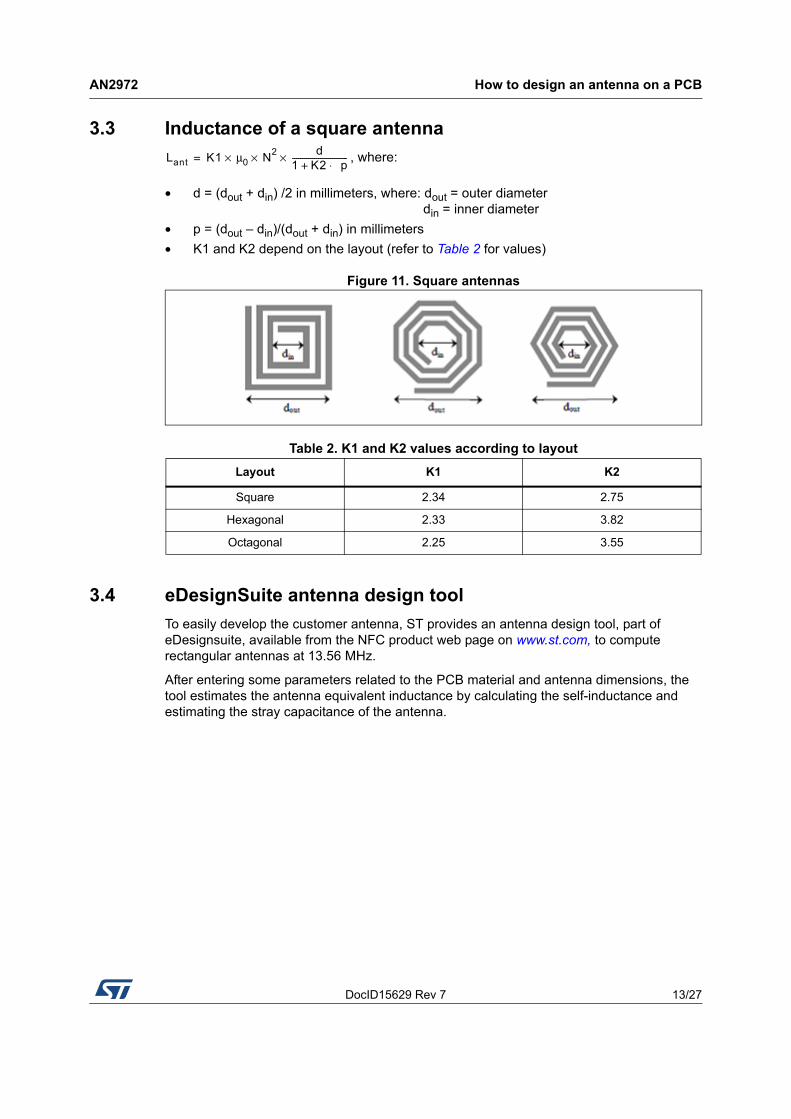
3.3 Inductance of a square antenna
, where:
• d = (dout + din) /2 in millimeters, where: dout = outer diameter din = inner diameter
• p = (dout – din)/(dout + din) in millimeters
• K1 and K2 depend on the layout (refer to Table 2 for values)
Figure 11. Square antennas
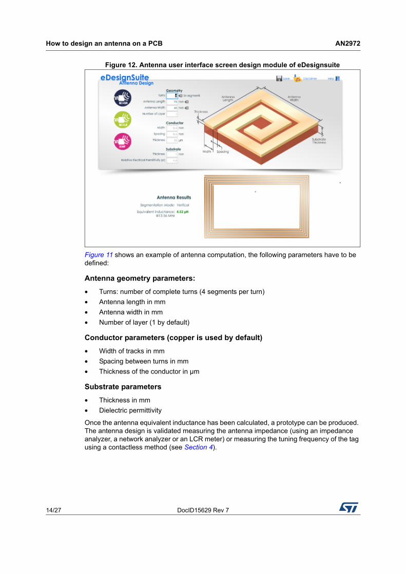
3.4 eDesignSuite antenna design tool
To easily develop the customer antenna, ST provides an antenna design tool, part of eDesignsuite, available from the NFC product web page on www.st.com, to compute rectangular antennas at 13.56 MHz.
After entering some parameters related to the PCB material and antenna dimensions, the tool estimates the antenna equivalent inductance by calculating the self-inductance and estimating the stray capacitance of the antenna.
Table 2. K1 and K2 values according to layout
Layout K1 K2
Square 2.34 2.75
Hexagonal 2.33 3.82
Octagonal 2.25 3.55
How to design an antenna on a PCB AN2972
14/27 DocID15629 Rev 7
Figure 12. Antenna user interface screen design module of eDesignsuite
Figure 11 shows an example of antenna computation, the following parameters have to be defined:
Antenna geometry parameters:
• Turns: number of complete turns (4 segments per turn)
• Antenna length in mm
• Antenna width in mm
• Number of layer (1 by default)
Conductor parameters (copper is used by default)
• Width of tracks in mm
• Spacing between turns in mm
• Thickness of the conductor in µm
Substrate parameters
• Thickness in mm
• Dielectric permittivity
Once the antenna equivalent inductance has been calculated, a prototype can be produced. The antenna design is validated measuring the antenna impedance (using an impedance analyzer, a network analyzer or an LCR meter) or measuring the tuning frequency of the tag using a contactless method (see Section 4).
DocID15629 Rev 7 15/27
AN2972 How to design an antenna on a PCB
26
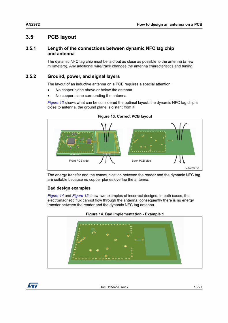
3.5 PCB layout
3.5.1 Length of the connections between dynamic NFC tag chip and antenna
The dynamic NFC tag chip must be laid out as close as possible to the antenna (a few millimeters). Any additional wire/trace changes the antenna characteristics and tuning.
3.5.2 Ground, power, and signal layers
The layout of an inductive antenna on a PCB requires a special attention:
• No copper plane above or below the antenna
• No copper plane surrounding the antenna
Figure 13 shows what can be considered the optimal layout: the dynamic NFC tag chip is close to antenna, the ground plane is distant from it.
Figure 13. Correct PCB layout
The energy transfer and the communication between the reader and the dynamic NFC tag are suitable because no copper planes overlap the antenna.
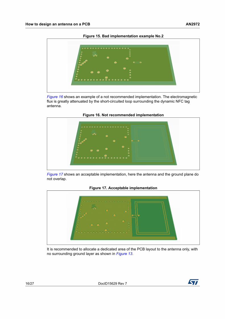
Bad design examples
Figure 14 and Figure 15 show two examples of incorrect designs. In both cases, the electromagnetic flux cannot flow through the antenna, consequently there is no energy transfer between the reader and the dynamic NFC tag antenna.
Figure 14. Bad implementation - Example 1
How to design an antenna on a PCB AN2972
16/27 DocID15629 Rev 7
Figure 15. Bad implementation example No.2
Figure 16 shows an example of a not recommended implementation. The electromagnetic flux is greatly attenuated by the short-circuited loop surrounding the dynamic NFC tag antenna.
Figure 16. Not recommended implementation
Figure 17 shows an acceptable implementation, here the antenna and the ground plane do not overlap.
Figure 17. Acceptable implementation
It is recommended to allocate a dedicated area of the PCB layout to the antenna only, with no surrounding ground layer as shown in Figure 13.
DocID15629 Rev 7 17/27
AN2972 How to design an antenna on a PCB
26
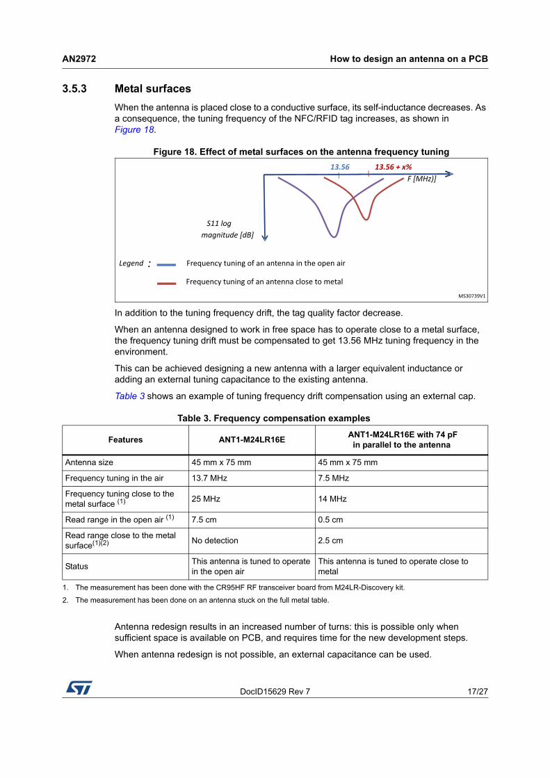
3.5.3 Metal surfaces
When the antenna is placed close to a conductive surface, its self-inductance decreases. As a consequence, the tuning frequency of the NFC/RFID tag increases, as shown in Figure 18.
Figure 18. Effect of metal surfaces on the antenna frequency tuning
In addition to the tuning frequency drift, the tag quality factor decrease.
When an antenna designed to work in free space has to operate close to a metal surface, the frequency tuning drift must be compensated to get 13.56 MHz tuning frequency in the environment.
This can be achieved designing a new antenna with a larger equivalent inductance or adding an external tuning capacitance to the existing antenna.
Table 3 shows an example of tuning frequency drift compensation using an external cap.
Antenna redesign results in an increased number of turns: this is possible only when sufficient space is available on PCB, and requires time for the new development steps.
When antenna redesign is not possible, an external capacitance can be used.
Table 3. Frequency compensation examples
Features ANT1-M24LR16E ANT1-M24LR16E with 74 pF
in parallel to the antenna
Antenna size 45 mm x 75 mm 45 mm x 75 mm
Frequency tuning in the air 13.7 MHz 7.5 MHz
Frequency tuning close to the metal surface (1) 25 MHz 14 MHz
Read range in the open air (1) 7.5 cm 0.5 cm
Read range close to the metal surface(1)(2) No detection 2.5 cm
StatusThis antenna is tuned to operate in the open air
This antenna is tuned to operate close to metal
1. The measurement has been done with the CR95HF RF transceiver board from M24LR-Discovery kit.
2. The measurement has been done on an antenna stuck on the full metal table.
How to check the NFC/RFID dynamic NFC tag antenna tuning AN2972
18/27 DocID15629 Rev 7
4 How to check the NFC/RFID dynamic NFC tag antenna tuning
Different parameters can impact the tuning frequency of the NFC/RFID tag:
• Antenna equivalent inductance computation precision
• Length of the connexion between the device and its antenna in application
• Antenna environment (metal surface, ferromagnetic material close to the antenna)
It is, consequently, necessary to check the resonant frequency of the NFC/RFID tag by measurement in final application conditions.
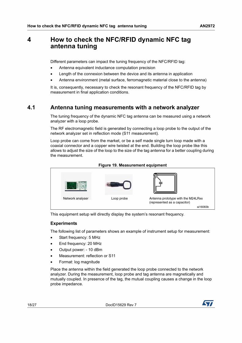
4.1 Antenna tuning measurements with a network analyzer
The tuning frequency of the dynamic NFC tag antenna can be measured using a network analyzer with a loop probe.
The RF electromagnetic field is generated by connecting a loop probe to the output of the network analyzer set in reflection mode (S11 measurement).
Loop probe can come from the market, or be a self made single turn loop made with a coaxial connector and a copper wire twisted at the end. Building the loop probe like this allows to adjust the size of the loop to the size of the tag antenna for a better coupling during the measurement.
Figure 19. Measurement equipment
This equipment setup will directly display the system’s resonant frequency.
Experiments
The following list of parameters shows an example of instrument setup for measurement:
• Start frequency: 5 MHz
• End frequency: 20 MHz
• Output power: - 10 dBm
• Measurement: reflection or S11
• Format: log magnitude
Place the antenna within the field generated the loop probe connected to the network analyzer. During the measurement, loop probe and tag antenna are magnetically and mutually coupled. In presence of the tag, the mutual coupling causes a change in the loop probe impedance.
DocID15629 Rev 7 19/27
AN2972 How to check the NFC/RFID dynamic NFC tag antenna tuning
26
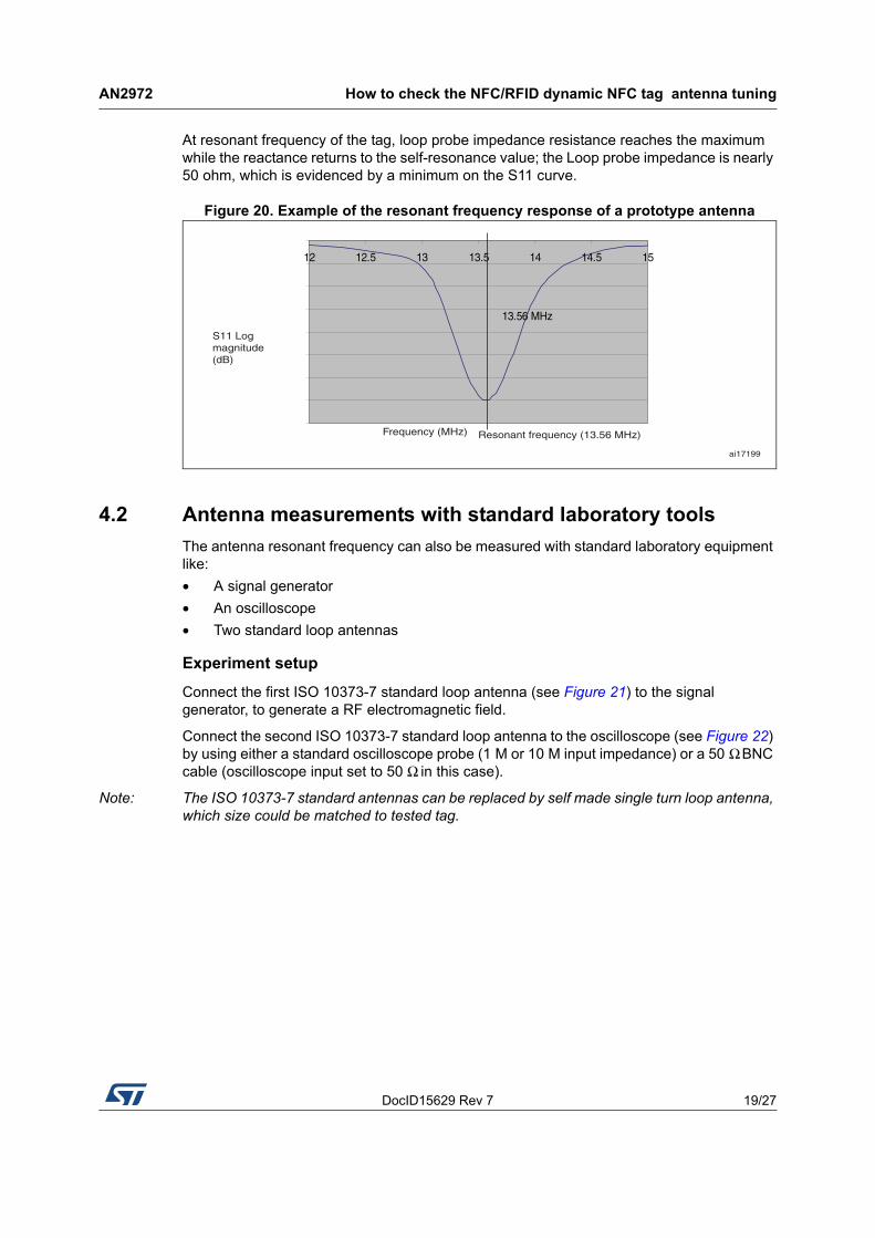
At resonant frequency of the tag, loop probe impedance resistance reaches the maximum while the reactance returns to the self-resonance value; the Loop probe impedance is nearly 50 ohm, which is evidenced by a minimum on the S11 curve.
Figure 20. Example of the resonant frequency response of a prototype antenna
4.2 Antenna measurements with standard laboratory tools
The antenna resonant frequency can also be measured with standard laboratory equipment like:
• A signal generator
• An oscilloscope
• Two standard loop antennas
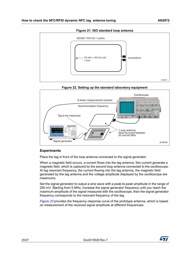
Experiment setup
Connect the first ISO 10373-7 standard loop antenna (see Figure 21) to the signal generator, to generate a RF electromagnetic field.
Connect the second ISO 10373-7 standard loop antenna to the oscilloscope (see Figure 22) by using either a standard oscilloscope probe (1 M or 10 M input impedance) or a 50 Ω BNC cable (oscilloscope input set to 50 Ω in this case).
Note: The ISO 10373-7 standard antennas can be replaced by self made single turn loop antenna, which size could be matched to tested tag.
S11 Logmagnitude(dB)
ai17199
12 12.5 13 13.5 14 14.5 15
13.56 MHz
Frequency (MHz) Resonant frequency (13.56 MHz)
How to check the NFC/RFID dynamic NFC tag antenna tuning AN2972
20/27 DocID15629 Rev 7
Figure 21. ISO standard loop antenna
Figure 22. Setting up the standard laboratory equipment
Experiments
Place the tag in front of the loop antenna connected to the signal generator.
When a magnetic field occurs, a current flows into the tag antenna, this current generate a magnetic field, which is captured by the second loop antenna connected to the oscilloscope. At tag resonant frequency, the current flowing into the tag antenna, the magnetic field generated by the tag antenna and the voltage amplitude displayed by the oscilloscope are maximums.
Set the signal generator to output a sine wave with a peak-to-peak amplitude in the range of 200 mV. Starting from 5 MHz, increase the signal generator frequency until you reach the maximum amplitude of the signal measured with the oscilloscope, then the signal generator frequency corresponds to the resonant frequency of the tag.
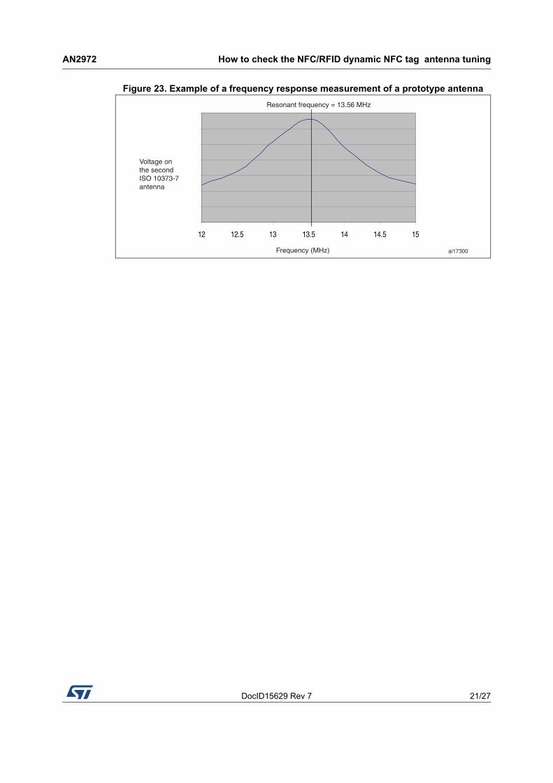
Figure 23 provides the frequency response curve of the prototype antenna, which is based on measurement of the received signal amplitude at different frequencies.
i15819
ISO/IEC 7810 ID-1 outline
connections72 mm × 42 mm coil1 turn
DocID15629 Rev 7 21/27
AN2972 How to check the NFC/RFID dynamic NFC tag antenna tuning
26
Figure 23. Example of a frequency response measurement of a prototype antenna
12 12.5 13 13.5 14 14.5 15
Frequency (MHz)
Resonant frequency = 13.56 MHz
Voltage onthe secondISO 10373-7antenna
ai17300
From design to production AN2972
22/27 DocID15629 Rev 7
5 From design to production
Designers should expect some difference between the theoretical and the real performance of the antenna on the PCB in the end application.
Here are a few considerations:
System level validation
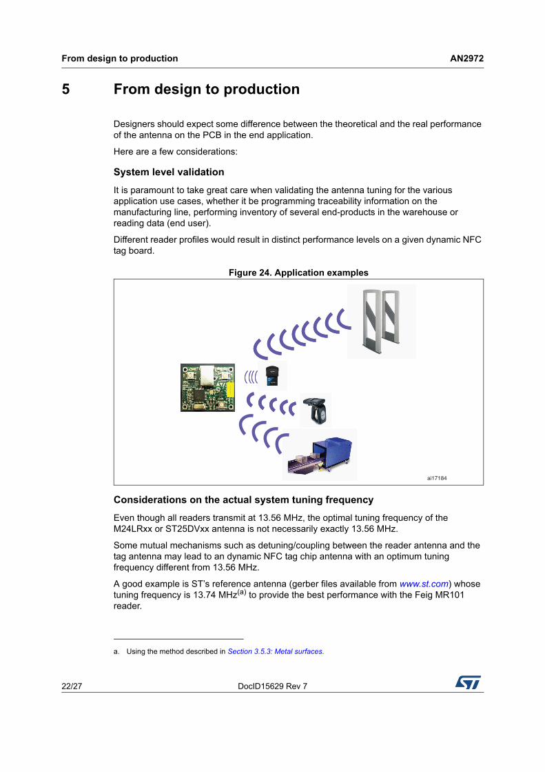
It is paramount to take great care when validating the antenna tuning for the various application use cases, whether it be programming traceability information on the manufacturing line, performing inventory of several end-products in the warehouse or reading data (end user).
Different reader profiles would result in distinct performance levels on a given dynamic NFC tag board.
Figure 24. Application examples
Considerations on the actual system tuning frequency
Even though all readers transmit at 13.56 MHz, the optimal tuning frequency of the M24LRxx or ST25DVxx antenna is not necessarily exactly 13.56 MHz.
Some mutual mechanisms such as detuning/coupling between the reader antenna and the tag antenna may lead to an dynamic NFC tag chip antenna with an optimum tuning frequency different from 13.56 MHz.
A good example is ST’s reference antenna (gerber files available from www.st.com) whose tuning frequency is 13.74 MHz(a) to provide the best performance with the Feig MR101 reader.
a. Using the method described in Section 3.5.3: Metal surfaces.
ai17184
DocID15629 Rev 7 23/27
AN2972 From design to production
26
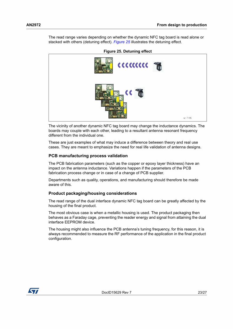
The read range varies depending on whether the dynamic NFC tag board is read alone or stacked with others (detuning effect). Figure 25 illustrates the detuning effect.
Figure 25. Detuning effect
The vicinity of another dynamic NFC tag board may change the inductance dynamics. The boards may couple with each other, leading to a resultant antenna resonant frequency different from the individual one.
These are just examples of what may induce a difference between theory and real use cases. They are meant to emphasize the need for real life validation of antenna designs.
PCB manufacturing process validation
The PCB fabrication parameters (such as the copper or epoxy layer thickness) have an impact on the antenna inductance. Variations happen if the parameters of the PCB fabrication process change or in case of a change of PCB supplier.
Departments such as quality, operations, and manufacturing should therefore be made aware of this.
Product packaging/housing considerations
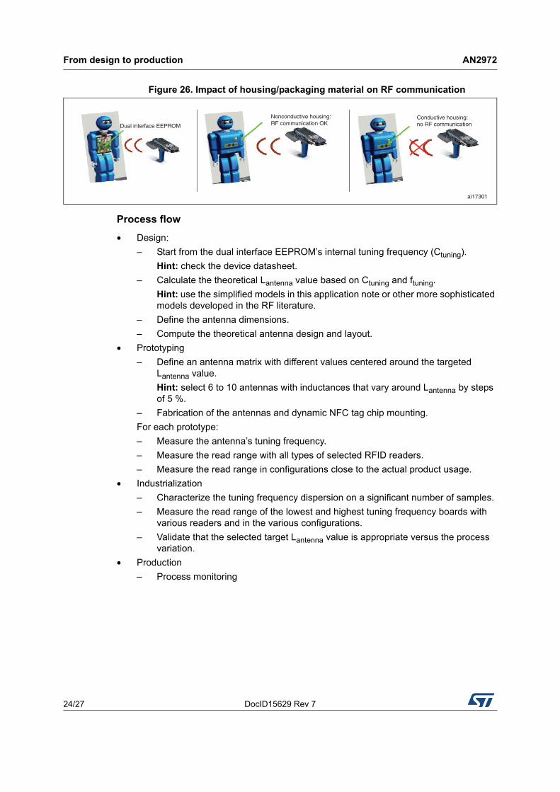
The read range of the dual interface dynamic NFC tag board can be greatly affected by the housing of the final product.
The most obvious case is when a metallic housing is used. The product packaging then behaves as a Faraday cage, preventing the reader energy and signal from attaining the dual interface EEPROM device.
The housing might also influence the PCB antenna’s tuning frequency, for this reason, it is always recommended to measure the RF performance of the application in the final product configuration.
From design to production AN2972
24/27 DocID15629 Rev 7
Figure 26. Impact of housing/packaging material on RF communication
Process flow
• Design:
– Start from the dual interface EEPROM’s internal tuning frequency (Ctuning).
Hint: check the device datasheet.
– Calculate the theoretical Lantenna value based on Ctuning and ftuning.
Hint: use the simplified models in this application note or other more sophisticated models developed in the RF literature.
– Define the antenna dimensions.
– Compute the theoretical antenna design and layout.
• Prototyping
– Define an antenna matrix with different values centered around the targeted Lantenna value.
Hint: select 6 to 10 antennas with inductances that vary around Lantenna by steps of 5 %.
– Fabrication of the antennas and dynamic NFC tag chip mounting.
For each prototype:
– Measure the antenna’s tuning frequency.
– Measure the read range with all types of selected RFID readers.
– Measure the read range in configurations close to the actual product usage.
• Industrialization
– Characterize the tuning frequency dispersion on a significant number of samples.
– Measure the read range of the lowest and highest tuning frequency boards with various readers and in the various configurations.
– Validate that the selected target Lantenna value is appropriate versus the process variation.
• Production
– Process monitoring
ai17301
Dual interface EEPROM
Nonconductive housing:RF communication OK
Conductive housing:no RF communication
DocID15629 Rev 7 25/27
AN2972 Revision history
26
6 Revision history
Table 4. Document revision history
Date Revision Changes
26-May-2009 1 Initial release.
06-Aug-2009 2
Modified:
– Introduction
– Section 2.1: Passive RFID technology
– Section 2.2: Simplified equivalent inlay circuit
– Section 2.4: Optimum antenna tuning
– Section 3.3: Inductance of a square antenna
Added: Section 5: From design to production
18-Aug-2009 3Corrected equation allowing to compute the tuning frequency on cover page.
04-Sep-2009 4
Figure 3: Dynamic NFC tag chip power mechanism in RF mode, Figure 5: Communication from the reader to the tag and Figure 6: Communication from tag to the reader modified.
Section 3.5: PCB layout added.
Section 4.1: Antenna tuning measurements with a network analyzer and Section 4.2: Antenna measurements with standard laboratory tools modified.
Considerations on the actual system tuning frequency added. PCB manufacturing process validation modified.
Product packaging/housing considerations and Process flow added.
Small text changes.
11-Feb-2010 5
Document classification level changed to public.
Power transfer updated in Section 2.1: Passive RFID technology.
Section 2.4 title modified.
Revision history AN2972
26/27 DocID15629 Rev 7
21-Dec-2012 6
M24LR64-R replaced by M24LRxx-R and M24LRxxE-R on the cover page, then by M24LRxx (see Note:).
Moved former 3rd and 4th paragraphs on the cover page to an 1Operating mode section.
Added Table 1: Applicable products.
Added Section 3.5.3: Metal surfaces.
17-Jan-2017 7
Updated:
– Introduction
– Section 1: Operating mode
– Section 2: Basic principles and equations
– Section 3: How to design an antenna on a PCB
– Section 4: How to check the NFC/RFID dynamic NFC tag antenna tuning
– Figure 1: Dynamic NFC tags
– Figure 3: Dynamic NFC tag chip power mechanism in RF mode
– Figure 4: Power transfer versus reader/dynamic NFC tag orientation
– Figure 5: Communication from the reader to the tag
– Figure 6: Communication from tag to the reader
– Figure 7: Equivalent circuit of the dynamic NFC tag chip and its antenna
– Figure 8: Equivalent circuit of the dynamic NFC tag chip mounted on a loop antenna
– Figure 11: Square antennas
– Figure 13: Correct PCB layout
– Figure 14: Bad implementation - Example 1
– Figure 15: Bad implementation example No.2
– Figure 16: Not recommended implementation
– Figure 17: Acceptable implementation
– Figure 22: Setting up the standard laboratory equipment
– Table 1: Applicable products
– Table 3: Frequency compensation examples
Table 4. Document revision history (continued)
Date Revision Changes

DocID15629 Rev 7 27/27
AN2972
27
IMPORTANT NOTICE – PLEASE READ CAREFULLY
STMicroelectronics NV and its subsidiaries (“ST”) reserve the right to make changes, corrections, enhancements, modifications, and improvements to ST products and/or to this document at any time without notice. Purchasers should obtain the latest relevant information on ST products before placing orders. ST products are sold pursuant to ST’s terms and conditions of sale in place at the time of order acknowledgement.
Purchasers are solely responsible for the choice, selection, and use of ST products and ST assumes no liability for application assistance or the design of Purchasers’ products.
No license, express or implied, to any intellectual property right is granted by ST herein.
Resale of ST products with provisions different from the information set forth herein shall void any warranty granted by ST for such product.
ST and the ST logo are trademarks of ST. All other product or service names are the property of their respective owners.
Information in this document supersedes and replaces information previously supplied in any prior versions of this document.
© 2017 STMicroelectronics – All rights reserved