how molecular doping affects the charge separation process ... · the charge separation process in...
TRANSCRIPT

How molecular doping affects
the charge separation process in
polymer-fullerene blends
München 2012


How molecular doping affects
the charge separation process in
polymer-fullerene blends
Dissertation
submitted to the Physics Department
of the Ludwig-Maximilians-Universität München
by
Felix Alexander Deschler
of
Bayreuth, Germany
München, 14th
December 2012


v
v
Cover picture:
SEM image of a dropcasted PCPDTBT film. The sketch displays a schematic
representation of a charge transfer exciton in a polymer-fullerene blend. The dopant
molecules F4TCNQ and oxygen are shown.
First reviewer: Prof. Dr. Jochen Feldmann
Second reviewer: Prof. Dr. Müller-Buschbaum
Additional members of the examination: Prof. Dr. Lode Pollet
PD Dr. Stefan Ludwig
Date of the oral examination: 01.02.2013


vii
vii
Learn from yesterday, live for today, hope for tomorrow.
The important thing is to not stop questioning.
Albert Einstein


ix
ix
Publications presented in this thesis
Deschler F., Da Como E., Limmer T., Tautz R., Godde T., Bayer M., von Hauff E.,
Yilmaz S., Allard S., Scherf U., Feldmann J.
Reduced Charge Transfer Exciton Recombination in Organic Semiconductor
Heterojunctions by Molecular Doping
Physical Review Letters 107, 127402. (2011)
Deschler F., De Sio A., von Hauff E., Kutka P., Sauermann T., Egelhaaf H.-J., Hauch J.,
Da Como E.
The Effect of Ageing on Exciton Dynamics, Charge Separation, and Recombination in
P3HT/PCBM Photovoltaic Blends.
Advanced Functional Materials 22, 1461–1469. (2012)
Deschler F., Riedel D., Deák A., Da Como E.
Imaging morphology changes and phase segregation in doped polymeric
semiconductors with low-voltage SEM
submitted (2012)
Further publications
Deschler F., Riedel D., Ecker B., Da Como E., von Hauff E., MacKenzie R.
Increasing organic solar cell efficiency with polymer interlayers
Phys. Chem. Chem. Phys., DOI: 10.1039/c2cp43876c, (2012)
Tunc A.V., De Sio A., Riedel D., Deschler F., Da Como E., Parisi J., von Hauff E.
Molecular doping of low-bandgap-polymer:fullerene solar cells: Effects on transport
and solar cells.
Organic Electronics 13, 290–296. (2012)

x
x
De Sio A., Madena T., Huber R., Parisi J., Neyshtadt S., Deschler F., Da Como E.,
Esposito S., von Hauff E.
Solvent additives for tuning the photovoltaic properties of polymer–fullerene solar cells.
Solar Energy Materials and Solar Cells 95, 3536–3542. (2011)
Hallermann M., Deschler F., Berger J, von Hauff E., Da Como E.
Dynamics of Charge Transfer Excitons Recombination in Polymer/Fullerene Solar
Cells
Material Research Society Proceedings 1286 (2011)
Contributions to conferences and workshops
Oral presentations
Deschler F., Da Como E, Feldmann J.
Enhanced exciton dissociation in doped organic semiconductors,
Light Harvesting Processes 2011, Kloster Banz, Germany
Deschler F., Da Como E, Feldmann J.
Enhanced charge separation in polymer/fullerene heterojunctions by molecular doping
SPIE Photonics West 2011, San Diego, CA, US
Deschler F., Riedel D., Da Como E, Feldmann J.
Doping as a new approach for charge generation in polymer-fullerene solarcells
Material Research Society Spring Meeting 2012, San Francisco, CA, US
Poster presentations
Deschler F., Tautz R., Hallermann M., von Hauff E., Da Como E., and Feldmann J.
Charge transfer excitons in conjugated polymer/fullerene blends
DFG Schwerpunktprogramm 1355 Winter School 2010, Bad Schandau, Germany
Deschler F., Da Como
E., De Sio A., von Hauff E., Egelhaaf H.-J.
Identification and quantification of loss processes in aged P3HT/PCBM blends
Material Research Society Spring Meeting 2012, San Francisco, CA, US

xi
xi
Deschler F., Da Como
E., De Sio A., von Hauff E., Egelhaaf H.-J.
The Effect of Ageing on Exciton Dynamics, Charge Separation, and Recombination in
P3HT/PCBM Photovoltaic Blends
Gordon Research Conference Electronic Processes in Organic Materials 2012,
Lucca, Italy


xiii
xiii
Kurzfassung
Diese Arbeit untersucht den Effekt niedermolekularen Dopings auf den Ladungstrennungsprozess in
organischen Halbleiter-Heteroübergängen. Zur Klärung der grundlegenden Mechanismen werden
verschiedene Dopanten und ihr förderlicher sowie nachteiliger Einfluss untersucht. Die gefundenen
Erkenntnisse bieten aussichtsreiche Ansätze zur Verbesserung der Leistung organischer Solarzellen.
Der erste Teil dieser Arbeit zeigt Niederspannungs-Rasterelektronenmikroskopie (REM) als neue
Methode zur hochauflösenden Detektion von p-Typ Dopanten-Verteilungen in konjugierten
Polymer-Filmen. Diese Studie hat das Ziel den Effekt von Doping auf die Morphologie von
organischen Halbleitern zu untersuchen. Dopantreiche Regionen werden in REM Bildern als helle
Bereiche detektiert. Photolumineszenz(PL)-Kartierung bestätigt die Zuordnung dopantreicher
Regionen, da ein Vergleich der dopantinduzierten PL-Quenching-Strukturen mit den, in REM
beobachteten, Dopantverteilungen Domänen mit vergleichbarer Form und Größe zeigt. Selektives
Aufladen dopantreicher Bereiche durch den Elektronstrahl wird als grundlegender Mechanismus des
erhöhten REM Kontrasts identifiziert. Das neue Detektionsprinzip wird verwendet, um den Effekt
von Doping auf die Morphologie zweier, für Solarzellen verwendeter, Polymere zu untersuchen
(PCPDTBT, P3HT). PCPDTBT weist, verglichen mit P3HT, eine homogenere Filmmophologie und
höhere Grenzwerte für Dopantclustering auf. Dies wird auf die Donor-Akzeptor Struktur von
PCPDTBT zurückgeführt, die elektrostatische Dopant-Polymer Interaktionen abschirmt.
Der zweite Teil untersucht den Effekt molekularen Dopings auf die Rekombination von Charge
transfer (CT) Exzitonen an der Grenzfläche von Polymer-Fulleren (PCPDTBT:PCBM) Blends.
Elektrontransfer von Polymer-HOMO zu Dopant-LUMO (F4CTNQ) führt zu p-Dotierung des
Polymers im Grundzustand. Niedrige Dopingkonzentrationen (<4% Gewicht) reduzieren die CT
Exziton Rekombination an der Grenzfläche and resultieren in einer bevorzugten
Ladunsgträgerbildung. Dies wird durch das ultra-schnelle Quenching der CT Exziton Emission in
zeitaufgelöster PL und die Zunahme der Polarondichte in zeitaufgelöster photoinduzierten
Absorption (PIA) beobachtet. Ein Fit der zeitaufgelösten PL und PIA mit einem
Ratengleichungsmodel signalisiert ferner eine, im Vergleich zur Polaronbildung, reduzierte CT
Exziton Bildungsrate, was zur beobachteten höheren Polarondichte führt. Die Resultate werden
durch dopinginduziertes Phasenraumfüllen und Blocken der niederenergetischen, unbeweglichen
Randzustände des Polymer-HOMOs erklärt. Solarzellen aus dotierten Blends erzeugen, in
Übereinstimmung mit den spektroskopischen Studien, einen erhöhten Photostrom. Diese
Erkenntnisse tragen zum grundlegenden Verständnis des Ladungstrennungsprozesses und der Rolle
von CT Exzitonen als Zwischenstufe bei. Zudem wird Elektronakzeptordoping als vielversprechende
neue Methode zur Verbesserung der Solarzellenleistung vorgestellt.
Das letzte Kapitel erforscht den nachteiligen Effekt von Sauerstoffdoping auf die Ladungstrennung
in P3HT:PCBM Blends mit spektroskopischen Methoden. Sauerstoffdoping unter Beleuchtung
bewirkt Photooxidation und p-Dotierung des Polymers, auch Degradation genannt. Die Auswirkung
auf die Exzitonpopulation wird durch Blend-Emissionsspektren für verschiedene Degradationsstufen
untersucht. Die Ergebnisse weisen auf eine, mit Degradation, linear zunehmende Dichte von
Quenchingstellen hin. Zur Untersuchung des Effekts von Sauerstoffdoping auf die Dynamik der
Ladungsträgerbildung werden Exziton- und Polaronpopulation mit zeitaufgelöster PIA untersucht.
Beide Populationen zeigen in degradierten Proben ein ultra-schnelles anfängliches Quenching und,
auf längeren Zeitskalen, eine schnellere Rekombination. Der Effekt ist jedoch stärker für Polaronen
ausgeprägt. Dies weist auf einen größeren Einfluss von Sauerstoffdoping an der Grenzfläche
zwischen Polymer und Fulleren hin, an der Ladungstrennung erfolgt. Ein Ratengleichungsmodel
wird verwendet um die zeitaufgelöste PIA zu fitten. Ultra-schnelles Einfangen von Exzitonen und
Polaronen an Degradationsstellen wird als zentraler Verlustmechanismus identifiziert. Diese
Ergebnisse tragen zum grundlegenden Verständnis der Degradation von organischen Solarzellen bei
und helfen neue Wege zu finden die Lebenszeit von Photovoltaikmodulen zu verlängern.


xv
xv
Abstract
This thesis investigates the effect of small molecule doping on the charge separation process in
organic semiconductor heterojunctions. To understand the underlying mechanisms, different
dopants and their beneficial and adverse impact on charge separation were investigated. The
insights from these results offer promising directions to improve organic solar cell performance.
In the first part, low-voltage scanning electron microscopy (SEM) is presented as a new
approach to map p-type dopant distributions in conjugated polymer films with high resolution.
This study is conducted to understand the effect of doping on the morphological properties of
the organic semiconductors. Dopant-rich regions are detected as bright areas in SEM images.
The assignment of dopant-rich regions is confirmed by photoluminescence (PL) mapping.
Comparison of dopant induced PL quenching patterns with the distributions observed in SEM
reveals domains with similar shape and size in both experiments. Additionally, site-selective
charging by the electron beam is identified as the underlying mechanism for the increased SEM
contrast. This novel mapping approach is employed to investigate the effect of doping on the
morphology of two polymers (PCPDTBT, P3HT), which are widely used in organic solar cells.
A more homogenous film morphology and a higher dopant clustering threshold is observed for
PCPDTBT, compared to P3HT. These findings are attributed to the special donor-acceptor
structure of PCPDTBT, screening the dopant-polymer electrostatic interaction.
The second part investigates the effect of molecular doping on the recombination of charge
transfer (CT) excitons localized at polymer–fullerene (PCPDTBT:PCBM) interfaces. Electron
transfer from the polymer HOMO (highest occupied molecular orbital) to the dopant (F4TCNQ)
LUMO (lowest unoccupied molecular orbital) leads to ground-state p-doping. A low dopant
concentration (<4% weight) reduces the interfacial recombination via CT excitons and results in
a favoured formation of separated carriers. This is observed by ultrafast quenching of CT
exciton emission in transient PL and an increase in polaron density in transient photoinduced
absorption (PIA). Furthermore, a rate equation model, used to fit the transient PL and PIA,
reveals a reduced rate of CT exciton compared to polaron formation, giving rise to the observed
increase in polaron yield. The results are interpreted on the basis of doping induced phase-space
filling and blocking of low-energy, immobile tail states in the polymer HOMO. Prototype solar
cells, fabricated from the doped blends, show an increase in photocurrent, in accordance with
the spectroscopic studies. These findings are important for the fundamental understanding of the
charge separation process and the role of CT excitons as intermediate steps. Further, electron
acceptor doping is presented as a promising method to improve organic solar cell performance.
The last chapter studies the adverse effect of oxygen doping on charge generation in
P3HT:PCBM blends with spectroscopic methods. Oxygen doping under illumination is known
to cause photo-oxidation and p-type doping of the polymer, termed degradation. The effects on
the exciton population are investigated from blend PL spectra for different degradation extents.
The results indicate a linearly increasing density of quenching sites with increasing degradation.
To address the effect of oxygen doping on the dynamics of charge formation, transient PIA is
employed to study exciton and polaron populations. With increasing degradation, both
populations exhibit an ultrafast initial quenching and a faster decay on longer time scales.
However, the effect is more severe for polarons. This indicates a more pronounced influence of
oxygen doping at the interface between polymer and fullerene, where charge separation occurs.
A rate equation model is used to fit the transient PIA. From this, ultra-fast trapping of excitons
and polarons at degradation sites is identified as the main loss mechanism. These results
contribute to the fundamental understanding of degradation processes in organic solar cells and
will help to find new ways to extend the lifetimes of organic photovoltaic modules.

xvii
xvii
Table of contents
Publications presented in this thesis ............................................................................. ix
Kurzfassung .................................................................................................................. xiii
Abstract .......................................................................................................................... xv
Table of contents ......................................................................................................... xvii
List of abbreviations ..................................................................................................... xx
1 The road to clean energy production from renewable sources ....................... 1
2 Fundamental concepts of photo-induced charge generation in organic
semiconductors .................................................................................................... 7
2.1 Molecules with delocalized π-electron systems .................................................... 8
2.2 Energy levels of organic semiconducting molecules .......................................... 11
2.3 Molecules in the solid state – the effects of disorder .......................................... 17
2.4 Neutral and charged excitations .......................................................................... 19
2.5 Optical transitions ................................................................................................ 22
2.6 Energy transport and exciton diffusion ............................................................... 26
2.7 Photogeneration of charge carriers in donor-acceptor blends ............................. 28
2.8 Charge transport in disordered systems ............................................................... 36
2.9 Basic principle of solar cell operation ................................................................. 37
3 Materials and Experimental Methods ............................................................. 41
3.1 Materials .............................................................................................................. 41
3.2 Sample fabrication ............................................................................................... 46
3.3 Experimental setups ............................................................................................. 49
4 Low-voltage Scanning Electron Microscopy Imaging of Doped Organic
Semiconductors Films ....................................................................................... 63
4.1 Motivation for dopant distribution mapping in polymeric organic
semiconductors .................................................................................................... 64
4.2 Morphological investigation of doped conjugated polymer films with AFM
and SEM .............................................................................................................. 65
4.3 Correlation of emission quenching patterns in PL maps with dopant
distributions in SEM images ............................................................................... 71
4.4 Monte-Carlo simulation of SEM electron yield from doped polymer films ....... 74

xviii
xviii
4.5 Explanation of contrast increase in SEM images based on site selective
charging of doped films ....................................................................................... 76
4.6 Conclusion ........................................................................................................... 78
5 Reduced charge transfer exciton recombination in doped organic
semiconductor heterojunctions ......................................................................... 79
5.1 Motivation to study the effect of changes in electronic structure on charge
separation ............................................................................................................. 80
5.2 Preparation of doped PCPDTBT:PCBM blend films .......................................... 80
5.3 Signature of polarons in absorption spectra of doped PCPDTBT:PCBM
films ..................................................................................................................... 83
5.4 Reduced CT exciton photoluminescence intensity with increasing doping
ratio ...................................................................................................................... 84
5.5 Ultra-fast initial quenching of CT exciton emission in time-resolved PL ........... 86
5.6 Increased polaron signal with increasing doping ratio in transient absorption
measurements of blend films ............................................................................... 89
5.7 Effect of doping on the polaron signal in transient absorption of PCPDTBT
films ..................................................................................................................... 92
5.8 Reduced CT exciton formation rate indicated by fitting of experimental
results with rate equation model .......................................................................... 93
5.9 Doping induced efficiency enhancement in solar cell performance .................... 96
5.10 Assignment of reduced CT exciton recombination loss in doped films to
phase space filling ................................................................................................ 98
5.11 Conclusion ......................................................................................................... 100
6 Effect of oxygen doping induced degradation on exciton dynamics and
charge separation in P3HT:PCBM blends .................................................... 101
6.1 Motivation to study oxygen doping induced degradation processes ................. 102
6.2 Controlled oxygen doping of polymer-fullerene blends .................................... 103
6.3 Observation of degradation-induced exciton population loss in steady state
photoluminescence ............................................................................................. 105
6.4 Reduced initial polaron and exciton populations with faster recombination
dynamics ............................................................................................................ 107
6.5 Quantification of loss processes with rate equation model ................................ 113
6.6 Effect of degradation on device performance .................................................... 117
6.7 Stronger effect of oxygen doping on polaron compared to exciton
populations ......................................................................................................... 118
6.8 Conclusion ......................................................................................................... 119
7 Summary and Outlook .................................................................................... 121
Appendix A .................................................................................................................. 125

xix
xix
References .................................................................................................................... 127
Acknowledgements ..................................................................................................... 141

xx
xx
List of abbreviations
AFM Atomic force microscopy
CCD Charge coupled device
CT exciton Charge transfer exciton
DOS Density of states
DP Delocalized polaron
F4-TCNQ 2,3,5,6-Tetrafluoro-7,7,8,8-tetracyanoquinodimethane
FF Fillfactor
GSB Ground state bleach
HOMO Highest occupied molecular orbital
ISC Short circuit current
LP Locliazed polaron
LUMO Lowest unoccupied molecular orbital
MIR Mid-infrared
NIR Near-infrared
NOPA Non-linear optical parametric amplifier
OLED Organic light emitting diode
OPA Optical parametric amplifier
P3HT Poly(3-hexylthiophen-2,5-diyl)
PCBM Phenyl-C61-butyric acid methyl ester
PCPDTBT Poly[2,1,3-benzothiadiazole-4,7-diyl[4,4-bis(2-ethylhexyl)-4H-
cyclopenta[2,1-b:3,4-b']dithiophene-2,6-diyl]]
PIA Photo-induced absorption
PL Photoluminescence
RPM Rounds per minute

xxi
xxi
SE Stimulated emission
SEM Scanning electron microscope
SHG Second harmonic generation
TA Transient absorption
TCNQ Tetracyanoquinodimethane
TEM Transmission electron microscope
TrA Triplet exciton absorption (T1Tn)
UV Ultraviolet
VOC Open circuit voltage
WL White light
YAG Yttrium aluminium garnet

1
1
1 The road to clean energy production from
renewable sources
On June 21, 1979 the 39th
President of the United States, Jimmy Carter, had 32 solar
panels installed on the roof of the White House. On the same day he gave a speech in
which he stated:
“A generation from now, this solar heater can either be a curiosity, a
museum piece, an example of a road not taken or it can be just a small part
of one of the greatest and most exciting adventures ever undertaken by the
American people.”
More than 30 years later, one has to conclude, that the road to regenerative energies,
mentioned by President Carter, has only been travelled partially. We are still underway
on this “exciting adventure” to clean energy production. The increasing need for clean
energy due to a rising world population and global warming remains an unsolved
problem. In 2011, only 4% of the global power consumption was provided from
regenerative energy sources like wind, water and solar energy 1. Advances in these
technologies are necessary to find energetically and economically sensible means for
power generation.
Current photovoltaic applications are mainly based on inorganic semiconductors such as
silicon. These have found widespread use as active material in transistors and computer
technology, and resulted in the rise of global computer technology companies.
However, the manufacture of efficient photovoltaic panels from silicon is quite
expensive and a substantial amount of energy has to be used during fabrication to melt
the inorganic semiconductors. This raises the question of alternative materials for
photovoltaic applications with more favourable properties. During the 20th
century a
new class of materials has been invented, which have found great interest in academia
and industry: organic semiconductors 2–4
. These materials are closely related to common
plastics, like e.g. polystyrene, and consist mainly of carbon atoms. It is possible to
design these materials by means of organic chemistry, which allows synthesising a
variety of different compounds. Additionally like other plastics, they can be fabricated

2
2
in almost every shape, are flexible and light- weight, and offer room temperature
processability with simple technologies, as for example ink-jet printing. So far these
materials have found everyday application in organic light emitting diodes (OLEDs) for
displays and lighting 5,6
. Several companies already sell consumer products with OLEDs
for the mass market, like smartphones and tablet computers. These products show the
competitive advantage of organic semiconductors in applications, where weight
reduction and compactness are key factors.
In the last years, organic semiconductors have also found increasing use in photovoltaic
applications. Starting from a low overall efficiency of around 2% in 2000, recently a
value of 10% has been reached 7,8
(Figure 1.1).
Figure 1.1 Improvement of maximum power conversion efficiencies for different
photovoltaic technologies measured under laboratory conditions from 1970 to 2012. The
inset shows a zoom on the development of organic solar cells (full circles) in the last
years. Image adapted from www.nrel.gov.
Despite these advances, silicon solar panels still show a significantly higher power
conversion efficiency of above 20% 9. Further advances are therefore necessary to bring
the promising organic photovoltaic technology into the market. Two critical missing
requirements for mass market application of organic photovoltaics are higher
efficiencies and long-term stability. Without improvements in power conversion
efficiency and lifetimes of panels of about 10 years, the market will not accept this new

Chapter 1 3
3
technology. It is the task of research to address these challenges. For power generation
the energy cost versus the energy produced is a critical parameter. For an optimal device
this ratio should be as small as possible. Especially in this respect, organic photovoltaics
present a promising technology, since their fabrication involves no energy-intensive
step, i.e. the melting and purification of silicon for standard solar cells. Just like last
century has been the century of silicon based technology, maybe the current century will
be the century of organic semiconductors, due to their fascinating properties and
promising applications at low cost.
One main step in solar cell operation is the conversion of absorbed photons into charge
carriers. In organic semiconductors this process involves the photo-excitation of
strongly bound excitons, which have to be separated into free charge carriers. The
present thesis studies the effects of small molecule doping on this charge separation
process in organic semiconductors. On the one hand, changes in the electronic structure
of a low-bandgap polymer:fullerene blend, induced by doping with electron acceptors,
are shown to reduce recombination via CT excitons and enhance charge separation. On
the other hand, degradation effects on exciton and polaron populations in polymer-
fullerene blends, induced from oxygen doping, are discussed. As one of the earliest
examples of doping in organic semiconductors, the conductivity of polyacetylene was
increased by exposure to iodine vapour 4 in 1977. In recent years, the topic of controlled
doping of polymer films with small electron acceptor molecules has been addressed
with focus on changes in the transport properties of the organic semiconductor 10,11
. In
parallel, other groups used dopant molecules to study the fundamental mechanisms of
charge transfer in highly ordered systems. For example, pentacene monolayers
including single dopant molecules were investigated with photoemission spectroscopy
and scanning tunnelling microscopy 12,13
. In summary, studies on the effect of doping in
organic semiconductors have been limited to transport phenomena or basic electronic
properties. It remains still an open question how doping affects other properties of
organic semiconductors besides transport. Therefore, this thesis investigates the effects
of small molecule doping on the charge separation process at the heterojunction of
conjugated polymer-fullerene blends.
The thesis is structured in the following way: In Chapter 2 we give an overview on the
fundamental theories relevant for photo-induced charge generation in organic
semiconductors. First, the general properties of organic semiconductors and their

4
4
differences compared to inorganic semiconductors are discussed. Subsequently, the
energy structure and the quantum mechanical description of the molecules’ energy
levels are presented. Additionally, the principal neutral and charged excitations are
described together with the optical transitions used to study these materials
spectroscopically. The possibility to transport energy in the material and the
corresponding theories are presented. Furthermore, the basic theory of photocarrier
generation is described based on the Onsager-Braun formalism. In the last section
charge transport and basic properties of solar cell operation are briefly outlined.
Chapter 3 gives an overview of the materials and methods employed. The basic
chemical and physical properties of the conjugated polymers PCPDTBT (Poly[2,1,3-
benzothiadiazole-4,7-diyl[4,4-bis(2-ethylhexyl)-4H-cyclopenta[2,1-b:3,4-']dithiophene-
2,6-diyl]]) and P3HT (Poly(3-hexylthiophen-2,5-diyl)) are described together with the
electron acceptor molecule PC60BM, which is a fullerene derivative. Additionally, the
small molecule dopant F4TCNQ (2,3,5,6-Tetrafluoro-7,7,8,8-tetracyanoquino-
dimethane) is introduced, which is a strong electron p-type dopant molecule. Further,
the fabrication of thin film samples from liquid solutions of the materials is described.
In the last section, the employed experimental techniques are outlined. The basic
principle of steady state and time resolved spectroscopic techniques are explained and
the microscopy setups, used to study the film morphology, are presented.
Chapter 4 deals with the influence of small molecule doping on the thin film
morphology of conjugated polymers. The effect of F4TCNQ incorporation on
PCPDTBT and P3HT films is studied with atomic force microscopy (AFM), scanning
electron microscopy (SEM) and confocal laser scanning photoluminescence (PL)
mapping. It is shown that the distribution of dopant molecules can be assessed from an
increased contrast between doped and undoped regions in low-voltage SEM images. In
the last part of this chapter, the physical origin of the increased contrast in SEM images
of doped films is discussed.
Chapter 5 discusses the effect of dopant induced changes in the electronic structure of
PCPDTBT:PCBM blends on the charge generation process. In particular, the impact of
doping on the recombination of charge transfer (CT) excitons is studied. Steady-state
and time-resolved PL spectroscopy are employed to study the CT exciton emission in
doped films. Concomitantly, the polaron yield is investigated from transient absorption
measurements. Furthermore, a rate equation model is employed to model the transient

Chapter 1 5
5
photoluminescence and transient absorption data. Finally, solar cells with doped
PCPDTBT:PCBM blends are presented, to compare the spectroscopic experiments with
solar cell performance.
Chapter 6 discusses the effects of oxygen doping on the photogeneration of charges in
P3HT:PCBM blends. Usually, oxygen doping has a detrimental effect on organic solar
cells, which is termed degradation. First, steady state absorption and photoluminescence
spectroscopy are used to quantify the effect of oxygen doping on excitons. Additionally,
the effect of degradation on the charge generation is investigated from transient
absorption experiments on excitons and polarons for different degradation levels. The
most relevant degradation mechanisms are identified from a rate equation model fitting
the transient absorption data. The spectroscopic results are compared with the
photovoltaic performance of degraded solar cells.
Chapter 7 summarizes the findings and gives an outlook on possible future experiments
and applications.


7
7
2 Fundamental concepts of photo-induced charge
generation in organic semiconductors
This chapter gives an overview on the theoretical background of the photo-induced
charge generation process in organic semiconductors: after absorption of photons in a
donor-acceptor blend, excitons are generated. These diffuse to the donor-acceptor
interface (heterojunction) by energy transfer in pure domains of the materials. Exciton
dissociation and charge generation primarily occurs at the heterojunction. In a solar
cell the generated charges are transported to the electrodes and extracted.
We start with a description of the general properties of organic semiconductors and
their basic properties. Theoretical methods to calculate the energy levels of organic
semiconductor molecules are explained and the respective neutral and charged
molecular excitations are presented. The optical excitation and the transport of energy
through the material are detailed. The photogeneration of charge carriers and the
relevant Onsager-Braun theory are discussed. The role of charge transfer excitons in
charge dissociation is outlined. In the last part, a short explanation of photovoltaic
operation and the critical solar cell parameters is given.

8
8
2.1 Molecules with delocalized π-electron systems
Organic semiconductors can be obtained in a variety of different molecular sizes. The
scale ranges from small molecules with less than ten atoms to large polymeric
macromolecules with more than hundred repeat units. Most of the research concerns
polymeric macromolecules with a delocalized electron system, which gives rise to semi-
conducting properties. Interestingly, these materials also exist in nature, with Melanin
being one important example. In 1963, Bolto and McNeill demonstrated that doping of
Melanin with iodine substantially increases its conductivity 2,3,14
. Thin films of synthetic
Melanin were fabricated in 1974 15
and in 1977 Shirakawa et al. achieved a large
change in conductivity by iodine doping of these synthetic polymers 16
. For these
discoveries, Shirakawa, Heeger and MacDiarmid were awarded the Nobel Prize in
Chemistry in 2000 17
. Besides the fundamental research on the electronic properties, in
recent years this class of materials also found applications in light-emitting diodes 18–20
,
photovoltaics 21–25
, field-effect transistors 26–29
and optically pumped lasers 30,31
. The
following paragraphs give an overview of the fundamental theories of organic
semiconductors, referring to the seminal literature 32–35
.
The main building blocks of organic semiconductors are carbon atoms. Due to a
delocalization of valence π-electrons, the molecules show semiconducting properties.
The reason for the delocalization lies in the special type of bonding between two carbon
atoms, described in the following. The ground state electron configuration of a carbon
atom is
. Hybridization of the orbitals occurs by forming three
degenerate sp2 orbitals from one s and two p orbitals, as shown in Figure 2.1.
Figure 2.1 Schematic representation of the orbitals in an sp2 hybridized carbon atom
seen from the side (a) and top (b). Yellow represents the hybrid orbitals while purple
shows the residual pz-orbital perpendicular to the plane of sp2 orbitals. Image adapted
from 36
.
(a) (b)

Chapter 2 9
9
The sp2 orbitals are coplanar and arranged at an angle of 120° to each other. The
residual 2pz orbital is perpendicular to the plane of hybrid orbitals. As an example how
hybridization leads to the formation of delocalized orbitals, the schematic orbital
geometry for ethene is shown in Figure 2.2. The bond between the carbon atoms is
created by the overlap of sp2 orbitals, forming σ-bonds, which are the strongest type of
covalent chemical bonds.
Figure 2.2 Schematic representation of the orbital structure in ethene (c). Yellow
represents the hybrid orbitals while purple shows the residual 2pz-orbitals perpendicular
to the plane of sp2 orbitals. σ-bonds are shown in (a), while π-bonds are depicted in (b).
Image adapted from 36
.
The remaining 2pz orbitals form a so called π-bond. Figure 2.2c depicts how the electron
density in the π-bond cannot be assigned to one carbon atom, but is spread along the
whole molecule above and below the central axis connecting the carbon atoms. This
delocalization of the electron density is called π-conjugation and is a characteristic of
organic semiconductors. Due to the lower overlap of the 2pz orbitals, the π-bonds are
much weaker and more polarizable than σ-bonds.
The overlap of two σ-(π-)orbitals from individual carbon atoms creates one bonding
σ-(π-)orbital and one anti-bonding σ*-(π*-)orbital (Figure 2.3). In the ground state only
the bonding orbitals are populated with two electrons each, since the anti-bonding
orbitals are higher in energy. The lowest electronic transitions occur therefore between
the highest bonding and the lowest anti-bonding orbital, which are most commonly π-
and π*-orbitals. In general, the highest occupied molecular energy level is called highest
occupied molecular orbital (HOMO), while the next higher energetic level is called
lowest unoccupied molecular orbital (LUMO).

10
10
Figure 2.3 Sketch of the energy levels for atomic and molecular orbitals. The overlap of
two atomic σ-/π-orbitals generates binding (σ/π) and anti-binding (σ*/π*) molecular
orbitals, which are shifted in energy.
The concept of electron density delocalization is not limited to small molecules, but also
observed, and especially relevant, for larger molecules, i.e. benzene or anthracene,
where conjugated alternating bonds are found. Another important class of organic
semiconductors are conjugated polymers which show a delocalization of the electron
density along the backbone of the polymer chain. These materials have a substantial
higher molecular weight compared to small molecule organic semiconductors. One
model compound for conjugated polymers is polyacetylene. A significant feature of
conjugated polymers is the alteration of single and double carbon bonds along the chain
(Figure 2.4), which leads to the delocalisation of the electron density along the chain.
C
C
C
C
C
C
C
C
C
C
C
C
H
H
H
H
H
H
H
H
H
H
H
H
n
Figure 2.4 Chemical structure of the conjugated polymer polyacetylene with alternating
single and double bonds between carbon atoms, giving rise to delocalized electron
densities.
For a perfect infinite chain of alternating single and double bonds the overlap of orbitals
results in a semi-filled band of energies, which leads to metallic behaviour. However,
semiconducting properties are observed in conjugated polymers. Peierls showed that in
Chapter 2 11
11
a one-dimensional system with incompletely filled bands, instabilities cause a lattice
distortion which induces differences in bond lengths between single and double
bonds 37
. Accordingly the length of the elementary cell of the one-dimensional chain is
doubled, leading to an energy gap Eg between the bands of bonding and antibonding
orbital configurations of a conjugated polymer chain. For this reason conjugated
polymers behave like semiconductors rather than metals. The value of the energy gap
depends on the length over which the electron density is delocalized. However, for
conjugated polymers with a high molecular weight, the ideal case of delocalization over
the whole chain is not observed. After a certain number of repeat units the conjugation
is broken, e.g. by kinks in the planar configuration of the chain or by chemical defects,
resulting in a reduced conjugation length. Control of the conjugation length by varying
the size or conformation of the polymer allows tuning the energy gap in the range of
1.5 eV to 3 eV 33
.
2.2 Energy levels of organic semiconducting molecules
In order to understand the properties of organic semiconductors, knowledge about the
energy levels is critical. The starting point for these calculations is the time-independent
Schrödinger equation together with a suitable molecular Hamiltonian and an ansatz for
the wavefunction according to molecular orbital theory 38
. Due to the complexity of this
many-body system, involving the coordinates of all electrons and nuclei, simplifications
and approximations for the Hamiltonian and the wavefunction have to be employed to
obtain a solution.
2.2.1 General Hamiltonian for molecular systems
Let’s consider the case of a molecule with Nnuc atoms with atomic numbers
and Nel electrons with Cartesian coordinates rj for the jth
electron. The momentum of the
jth
electron is denoted with pj. The Cartesian coordinates and momenta for the nuclei are
Rn and Pn respectively. The general Hamiltonian operator for the system is then of the
form
(2-1)
Here the kinetic energy of electrons Tel and nuclei Tnuc is given by

12
12
∑
(2-2)
and
∑
(2-3)
respectively, with the electron mass mel and the mass of the nth
nucleus Mn. Due to the
negative charge of electrons and the positive charge of nuclei, attractive and repulsive
Coulomb forces have to be taken into account. The repulsive Coulomb pair interaction
between electrons is described by
∑
| |
(2-4)
and for nuclei by
∑
| |
(2-5)
Finally, for the attractive interaction of electrons and nuclei we have
∑
| |
(2-6)
All information about the quantum system is now contained in the time-independent
Schrödinger equation
( ) ( ) (2-7)
with the wavefunction ( ) and the eigenenergies . The quantum number σ had
to be introduced to account for the electron spin, since the non-relativistic Hamiltonian
(2-1) does not allow for a rigorous introduction of spin operators. The formulation of
the Cartesian coordinates was simplified as ( ) and
( ). Without knowing the explicit formulation of the wavefunction
( ), we can already make several statements about its general features:

Chapter 2 13
13
(1) From the spin-independent formulation of the molecular Hamiltonian (2-1) we
conclude that the wavefunction can be separated in two parts according to
( ) ( ) ( ) (2-8)
with ( ) being the spin function for the electrons. The values of the spin states
σj are either parallel (spin up) or antiparallel (spin down) to a certain spatial
direction.
(2) According to the Pauli principle the wavefunction of a system of electrons,
which are fermions, has to be antisymmetric under exchange of any two
electronic indices. This means that ( ) has to be antisymmetric in
Cartesian and spin coordinates. The fact that the Pauli principle applies also to
identical nuclei is often neglected, since the wavefunctions of nuclei are more
localized.
(3) The solutions of Equation (2-7) will give a series of eigenenergies with
corresponding eigenfunctions ( ). The lowest eigenenergy will
define the ground state of the system. These values are the molecular energy
levels.
2.2.2 Simplifications of the full molecular Hamiltonian
The Born-Oppenheimer approximation is the most critical simplification of the
molecular Hamiltonian and is based on the difference in electron and nuclear masses
( ⁄ ). This relation implies that electrons move much faster than the
nuclei and respond to changes in the nuclear configuration almost immediately. The
Born-Oppenheimer approach therefore assumes a constant nuclear distribution in which
the electrons move. With this, it is now possible to define a purely electronic
Hamiltonian, which only depends parametrically on the coordinates R of the nuclei:
( ) ( ) ( ) (2-9)
The solutions ( ) to the Schrödinger equation employing the electronic
Hamiltonian
( ) ( ) [ ( ) ] ( ) (2-10)

14
14
describe the motion of electrons in the static nuclear configuration. The nuclear-nuclear
interaction does not play a role in the calculation of the electronic
wavefunctions. It is simply a constant that arises on both sides of the equation and
cancels out, leading to the following Schrödinger equation for the electronic
wavefunctions:
[ ] ( ) ( ) ( ) (2-11)
The solutions to Equation (2-11) depend parametrically on the coordinates R. The index
a describes the different energy levels Ea and the corresponding wavefunction . The
full molecular wavefunction is now constructed using an expansion in the electronic
wavefunctions :
( ) ∑ ( ) ( )
(2-12)
The expansion coefficients ( ) are interpreted as the nuclear wavefunctions and are
found by solving the nuclear Schrödinger equation, neglecting non-adiabatic coupling
of electronic states with nuclear motion. This is essentially the Born-Oppenheimer
approximation:
[ ( )] ( ) ( ) (2-13)
In this equation ( ) represents an effective potential for the motion of the nuclei,
describing their mutual Coulombic interaction and the interaction with the electronic
charge distribution given by the electronic wavefunctions:
With these approximations we still have the quite complicated Hamiltonian of Equation
(2-9) to solve. However the complexity of the problem can be reduced by further
simplifications. For this it is convenient to write the electronic molecular Hamiltonian in
one- and two-particle terms:
∑
(| ⟩⟨ | | ⟩ ⟨ |) ∑
| ⟩⟨ | (2-15)
with the electronic one-particle part
( ) ( ) (2-14)

Chapter 2 15
15
∫
( ) [
( )] ( ) (2-16)
and the electronic two-particle part
∬
( ) ( )
( ) ( ) ( ) (2-17)
In these equations ( ) is the effective potential for electron-nucleus interactions,
describes the effective electron-electron interactions and is the
interaction between nuclei. The model with the most severe simplifications is Hückel
theory 39–41
where electron-electron interactions ( , and ( )), exchange
interactions ( ) and nuclear interactions are neglected. Additionally the
wavefunction is set as a linear combination of atomic orbitals (LCAO method). In a
slightly more complex model, electron-phonon interactions ( ( ) ) are
introduced, assuming only one mode coupling to the π-electrons. This is the Su-
Schrieffer-Heeger model 42
. Several other approximations exist, which differ in the
considered contributions of the electronic molecular Hamiltonian.
2.2.3 Solution of the Schrödinger equation with the Hartree-Fock method
Since the exact solution of the full electronic Hamiltonian (2-9) is only possible with
several approximations, methods to calculate solutions numerically have been derived.
The work-horse for these calculations is Hartree-Fock theory. One starts again from the
Schrödinger Equation (2-11), but the electronic wavefunction of the molecule is created
as a product of single-particle electron wavefunctions solving the equation
[ ( ) ( )] ( ) ( ) (2-18)
i.e. the interactions between electrons are switched off. The index α describes the
different energy levels and the corresponding wavefunctions .
Since we have to take the Pauli principle into account, the total wavefunction of the
system is supposed to be antisymmetric, so a Slater determinant is used to generate an
ansatz for the wavefunction of all N electrons:

16
16
( ) | ( ) ( )
( ) ( )| (2-19)
Employing the variational principle using the full Hamiltonian (2-9) and the
wavefunction from (2-19), one arrives at a set of coupled integro-differential
equations35
, the Hartree-Fock equations:
( ) ( ) ( ) (2-20)
with the Fock operator
( ) [ ( ) ( )] ∑[ ( ) ( )]
⁄
(2-21)
the Coulomb operator
( ) ∫| (
)| ( ) (2-22)
and the exchange operator
( ) ( ) [∫
( ) ( ) ( )] ( ) (2-23)
For a detailed derivation of these formulations, the reader is referred to the standard
literature 33,35
. In the Hartree-Fock equations the interaction of an individual electron
with the remaining electrons is only taken into account as an effective potential created
from the other electrons, as can be seen from Equation (2-22). The computational
calculation involves the iterative solution of the Fock equations, since the Fock operator
itself contains the orbitals ( ). Starting from some trial orbitals the Fock equations
are solved and the new orbitals are used to calculate an updated Fock operator, which is
again used to solve the Fock equations. This iteration is repeated until a self-consistent
solution is reached. Therefore this computational approach is termed Hartree-Fock self-
consistent field method.

Chapter 2 17
17
2.3 Molecules in the solid state – the effects of disorder
In the previous parapgraphs the properties of organic semiconductors on the level of
single molecules were described, taking only intramolecular forces into account. Going
from individual molecules to the solid state, intermolecular forces have to be
considered. In general, there are four types of intermolecular forces: Ionic bonds (long-
range Coulomb interactions in ionic crystals), metallic interactions (delocalized electron
gas), covalent bonding (sharing of electrons between molecules) and Van der Waals
forces (induced electrical dipole forces between neutral molecules). Because of the
absence of free electrons in organic semiconductors, mainly Van der Waals interactions
play a role. These interactions are attractive forces between two neutral, nonpolar
molecules due to temporally fluctuating charge distributions. The fluctuations induce
dipoles in neighbouring molecules, which results in an attractive force. On the other
hand, also repulsive forces exist, which are due to the Pauli principle. These forces
concern the interaction of electrons in corresponding orbitals but from different
molecules. The superposition of attractive and repulsive forces results in an overall
potential, which is modelled with the Lennard-Jones potential:
(2-24)
The terms A and C12 are independent of the molecules’ distance r and contain
information on the molecules’ properties, e.g. the ionisation energy. Only interactions
between neighbouring molecules will play a role, due to the strong dependence of the
potential on the intermolecular distance. Therefore, any long range interaction in
organic semiconductors is negligible. Crystal formation is limited to special cases or to
molecules with additional ionic contributions to the intermolecular forces. In these
systems a band-like energy structure is observed, given by a periodic potential in
analogy to inorganic semiconductors. However, the bandwidth is only of the order of a
few meV, due to the low intermolecular interactions compared to inorganics.
The typical conformation and structure of organic semiconductors in the solid state is
therefore amorphous with substantial disorder. Furthermore, due to the weak
intermolecular interaction, the properties of molecules in the solid state differ only
slightly from isolated molecules and many properties can be already derived from the
single isolated molecule properties as calculated from the models in Paragraph 2.2.
However, the disorder present in the film has an impact on the energy levels of the

18
18
individual molecules. First, every molecule is positioned in a different dielectric
environment, which affects the electronic states. A simple analogy is the energy shift of
molecular absorption spectra for different solvents. Second, every molecule differs
slightly in geometrical conformation, e.g. due to twists and kinks in the backbone for
the case of polymers, leading to a distribution of conjugation lengths and accordingly,
energy levels. The resulting shifts in molecular energies give rise to a Gaussian
distribution 43–45
of states around a most probable energy value (Figure 2.5a). The large
number of molecules in the film leads to a quasi-continuous distribution of energy
levels within the Gaussian broadened density of states. For this reason one often refers
to an “energy band”, however it is important to note that the origin of this “band” is not
due to a periodic potential, as for inorganic semiconductors, but to spatial disorder. The
Gaussian distribution of energy levels exists for neutral excitons as well as for charged
(polaron) states. The energy level distribution upon formation of an amorphous film is
shown in Figure 2.5b for the HOMO and LUMO levels. The energy level broadening
plays a critical role in the description of charge and energy transport phenomena as
discussed below.
Figure 2.5 (a) Schematic representation of the disorder induced Gaussian broadening of
the density of states for a molecular energy level in a disordered film. The maximum of
the distribution relates to the energy level of an isolated molecule. (b) Broadening of
HOMO and LUMO energy levels on the transition from the single isolated molecule to an
amorphous film.

Chapter 2 19
19
2.4 Neutral and charged excitations
2.4.1 Excitons
Optical excitation of an inorganic semiconductor generally leads to free charges,
because the high dielectric constant of the material screens the interaction of positive
and negative charges. In organic semiconductors the dielectric constant is low (ε ~ 3-4)
and electron-electron interactions are dominant. Therefore, once an electron is excited,
it forms in combination with the hole a bound state. This neutral excitation of the
system is termed exciton. The binding energy Eb of the exciton is defined by the
Coulomb attraction and is basically determined by the energy difference between the
bound electron-hole pair and the configuration corresponding to free charges. In
inorganic semiconductors the thermal energy kT is sufficient to separate the electron-
hole pair, while in organic semiconductors the exciton binding energy can be as high as
0.5 eV up to 1 eV 46–49
. Based on the spatial extension of the exciton, which depends on
the binding energy Eb, one differentiates different types of excitons (Figure 2.6). There
is the strongly delocalized Wannier-type exciton, which is usually found in inorganic
semiconductors. For this type of exciton, the radius of the electron-hole pair covers
several molecules or lattice sites.
Figure 2.6 Schematic representation of Frenkel, Wannier and CT excitons. Frenkel
excitons are localized on one molecule while Wannier and CT excitons are extended over
several molecules. Reproduced with permission from reference34
.
A second type of exciton is the strongly localized Frenkel exciton with a radius of 1 -
3 nm 50
. In this case, the electron-hole pair resides on one molecular site. This type of

20
20
exciton is most commonly observed in organic semiconductors. The lifetime of Frenkel
excitons can be rather long (ns to µs) and having the excitation a strong dipolar
momentum, it can move through the solid by energy transfer (see Paragraph 2.6). A last
type of exciton is called charge transfer exciton. In this case, the excited electron is
(partially) transferred to a neighbouring molecule, but remains bound to the hole on the
initially excited molecule. The charge transfer exciton is neutral, but has a pronounced
dipolar character. A more specific concept is the exciplex, which describes a delocalized
excitation over two neighbouring molecules from different species. Usually, the
molecules involved in the formation of the exciplex possess strong electron donor and
acceptor character, respectively. The energy of a CT exciton, , is given by
( ) ( ) (2-25)
with the ionisation potential of the donor , the electron affinity of the acceptor , the
polarisation energy ( ) of the surroundings, due to the electron hole pair with
separation r, and the Coulomb attractive energy ( ) between the electron and the hole.
CT excitons are difficult to observe in optical measurements due to their weak oscillator
strength 34
.
So far, we have not addressed the influence of spin on these excitations. The strong
electron-electron interactions in organic semiconductors lead to significant stabilization
of the triplet state and a lifting of the degeneracy between singlet and triplet states.
Since the triplet state consists of electrons with parallel spins and the Pauli principle
excludes two electrons in the same orbital, the electrons in a triplet state have to occupy
different orbitals. Therefore they are on average further separated, compared to singlet
electrons. As a result, the energy of the triplet is lowered with respect to the singlet due
to the reduced electron repulsion. The difference between the energies of singlet and
triplet is given by the exchange integral 51,52
. Notably, since CT excitons are spatially
more separated, the exchange interaction is lower compared to Frenkel excitons. This
leads to a reduced splitting between singlet and triplet CT excitons, affecting the
energetics and photophysics of the system. For example, the recombination of initial
singlet Frenkel excitons to triplets might be enhanced by intersystem crossing in an
intermediate CT exciton level 53
.

Chapter 2 21
21
2.4.2 Polarons
A charged state can be formed by addition/removal of an electron to/from the ground
state of the molecule. The low electrostatic screening in organic semiconductors allows
a polarisation of the material in the vicinity of the charge and a concomitant
deformation of the molecular structure. A localized charge surrounded by a region of
molecular distortion is formed. The quasiparticle describing the charge combined with
the molecular deformation is termed polaron 54,55
. The general concept of a polaron was
first introduced by Landau to describe an electron propagating in a polarizable lattice
carrying the lattice deformation with its position 56
(Figure 2.7).
Figure 2.7 Schematic representation of a polaron. A positively charged particle (red) in a
lattice of molecules (blue) polarizes the surroundings, which leads to displacement of the
molecules from their equilibrium positions (circles). The entity of charge and lattice
deformation is termed polaron.
Due to the strong coupling between charge and molecular vibrations in organic
semiconductors, only the environment in the close vicinity of the charge is affected,
leading to a “small” polaron. For the case of conjugated polymers the polaron involves a
deformation of the bond lengths in the molecule, i.e. along the polymer backbone.
Accordingly, a polaron has a certain polaron binding energy or reorganization energy,
which is related to the deformation-induced energy and additionally leads to a self-
localization of the charge. The energy levels of polarons are positioned between HOMO
and LUMO level of the organic semiconductor (Figure 2.8). Additional optical
transitions (P1, P2) are activated upon formation of polarons, allowing the investigation
of these states with spectroscopic tools 57,58
.

22
22
Figure 2.8 Schematic representation of polaron transitions for positively (radical cation)
and negatively (radical anion) charged molecules. For the cation one electron is removed
from the molecule while for anions an electron is added. Intraband transitions are
indicated as P1, while P2 denotes interband transitions.
The P1 transitions are in the energy region around 0.3 eV, while the P2 transitions are in
the near-infrared around 1 eV 59
. The energy of the P1 transition is a measure for the
relaxation in energy connected to the distortion of the molecular structure. It has been
found that the energy of the P1 transition is associated with the delocalization of the π-
electrons and the delocalization length can be related to the transition energy
based on ⁄ 60. Since polarons in organic semiconductors, in a
chemical description, are similar to a charged molecule, the expressions radical cation
(positively charged molecule) and radical anion (negatively charged molecule) are also
used to describe polarons.
2.5 Optical transitions
The energy difference between the ground state S0 and the first excited state S1 of
organic semiconductor molecules is usually in the range 1 - 3 eV, which enables
excitation of transitions with visible light. This allows us to study the electronic
structure of organic semiconductors with optical spectroscopic methods. Upon
excitation with light, the molecule undergoes a transition from the ground state to an
excited state. Eventually, emission might occur through the radiative relaxation of the
excited state. We limit our discussion to the case of transitions between the ground state
S0 and the first excited state S1. In Figure 2.9 the potential energy curves for the ground
and excited state are shown versus the molecular configuration coordinate Q. Excitation

Chapter 2 23
23
of the system leads to a reconfiguration of the electronic structure and a shift in the
position of the nuclei. Therefore, the electronic potential of the excited state is shifted
along the Q axis with respect to the ground state.
Figure 2.9 Energy diagram of the absorption (a) and emission (b) transitions (arrows) in a
two level system. The energy potentials for ground and excited state S0 and S1 are
plotted against the configuration coordinate Q. Vibrational modes are indicated as dotted
lines and energy levels within the electronic potential. Exemplary absorption and
emission spectra with vibronic progressions are shown in (c).
The small electron mass compared to the mass of the nuclei allows assuming that
electronic transitions initially do not affect the nuclear configuration (Born-
Oppenheimer approximation) and can be drawn as vertical lines in the energy diagram.
Since molecules feature different vibrational modes ν, both, in the ground and excited
state, transitions to these vibronic energy levels are possible. Absorption processes
occur from the lowest vibronic level of the ground state, since the thermal energy at
room temperature is not sufficient to populate the first vibrational mode S0,1, about
100meV above the lowest energy level S0,0. However, transitions to higher vibronic
modes in the first excited electronic state are possible. These are visible as progressions
above the energy of the S0,0S1,0 transition in the absorption spectrum (Figure 2.9c).
The transition probability of vibronic transitions is ultimately determined by the
wavefunction overlap for the initial and final state (Franck-Condon principle61,62
). This
is formally described by the following formula for the absorption coefficient

24
24
( ) |⟨ |∑
| ⟩|
∑
( ) (2-26)
with the so called Huang-Rhys parameter S, the frequency of the absorbed light ω, the
frequency of the vibrational mode ωvib, the order of the vibrational mode N and the
frequency correlating to the energy difference between initial and final state ωfi. The last
term indicates a delta function.
The derivation of Equation (2-26) is based on Fermi’s Golden Rule for the transition
rate between an initial state | ⟩ and a final state | ⟩
|⟨ |∑ ( )
| ⟩|
( ) (2-27)
with the electromagnetic field vector E(t) and the energies of the final and initial states
Ef, Ei. The Franck-Condon principle is a direct consequence of the Born-Oppenheimer
approximation. It has the effect, that changes in the nuclear wavefunction are neglected
for the calculation of the transition dipole moment . This leads to the simplified
expression
⟨ |∑
| ⟩ ⟨ | ⟩ (2-28)
with the instantaneous overlap of the nuclear wavefunctions ⟨ | ⟩ and the purely
electronic transition dipole operator . The right hand side of the equation shows the
factorization of the total vibronic wavefunction Ψ into the electronic ϕ and the
vibrational part χ. Equation (2-26) is finally obtained by evaluating the overlap of the
nuclear wavefunctions between the lowest vibrational state and higher
vibrational states N.
After excitation of an energy level S1,ν non-radiative decay processes lead to a fast
relaxation of the system to the lowest excited state S1,0 on a time scale of
10-13
s 33,34,63,64
. Therefore, emission processes are usually observed from the lowest
excited state S1,0 only. Just like for absorption, transitions are also possible to vibronic
levels of the ground state, giving rise to progressions at lower energies with respect to
the S0,0S1,0 transition. This is illustrated in Figure 2.9c. Spontaneous emission can be

Chapter 2 25
25
described by the Einstein spontaneous emission coefficient or again Fermi’s Golden
Rule. In both cases the transition rate is given by
| |
∑|⟨ | ⟩|
( )
(2-29)
The spectral shift between absorption and emission maxima (Figure 2.9) is known as
Stokes-Shift. The main reason for this effect lies in an energy loss due to relaxation of
the molecule after excitation. Also solvent effects, excited state effects or energy
transfer, e.g. in a broadened density of states, can play a role 65,66
.
So far, we have considered only a simple two level system and did not take the spin of
the excitation into account. The spin plays an important role in organic semiconductors
and gives rise to singlet and triplet states, as discussed in Paragraph 2.4.1. A convenient
way to represent the complete photo-physical processes is a so-called Jablonski diagram
(Figure 2.10). It shows the ground state S0 together with higher excited singlet states
S1/S2 and also triplet states T1/T2. Each level splits further into vibronic levels due to
coupling of the electrical states to molecular vibrations.
Figure 2.10 Jablonski diagram for the optical transitions in an organic semiconducting
molecule. Singlet (Si) and triplet levels (Ti) are shown together with absorption,
fluorescence and phosphorescence. Intersystem crossing occurs between singlet and
triplet levels.

26
26
Optical excitation from the ground state is only possible to excited singlet states due to
spin conservation rules. Once a higher lying state Si is created, fast non-radiative
internal relaxation among the electronic excited states occurs on a ps-time scale until the
first excited singlet state S1 is reached (Kasha’s rule) 32,33,67,68
. As discussed in
Paragraph 2.4.1, the energy of triplets is lowered by twice the amount of the exchange
integral compared to the singlet state 35,66
, i.e. about 0.8 eV 51,69
. Formally, transitions
from the singlet to triplet states are forbidden, since the spin conservation condition is
not fulfilled. However, spin-orbit coupling can make these transitions weakly allowed
and intersystem crossing occurs. For the same reason, the decay from the triplet to the
ground state (phosphorescence) is weakly allowed, with lifetimes of about 10-6
to 10-2
s.
On the other hand, the lifetimes corresponding to transitions from excited singlet states
to the ground state (fluorescence), are in the region of 10-9
to 10-7
s. The transition from
the S1 state to separated charges (charge dissociation) is an additional process which is
especially relevant for photovoltaic applications. A detailed discussion of this process is
given in Paragraph 2.7.
2.6 Energy transport and exciton diffusion
The existence of long-lived neutral excitations (excitons) in organic semiconductors
allows energy transfer between molecular sites. Energy transfer is of critical importance
for photovoltaic applications using organic semiconductors, since the primary
excitations in the polymer have to diffuse to the heterojunction between donor and
acceptor for efficient charge separation. Exciton transfer processes are described by
hopping of an exciton from one molecule to the other. Energy transfer can take place
either between different types of molecules with donor and acceptor properties, or
within the Gaussian broadened density of states of a pure organic semiconductor 63,70
.
The physical property describing the range of energy transfer is the exciton diffusion
length, which gives a value for the distance an exciton can travel before recombining. A
typical method to experimentally determine values for the exciton diffusion length is the
measurement of photoluminescence quenching in donor-acceptor bilayers as a function
of layer thickness 71
. The obtained values depend on the investigated material and are,
for example, in the range of 3 - 9 nm for P3HT films. The radiation-less energy transfer
can either occur due to dipole-dipole interactions (Förster mechanism) or based on
electron exchange interactions (Dexter mechanism).

Chapter 2 27
27
In Förster theory 72,73
the transfer rate between a Donor (D) and acceptor (A)
molecule is given by
(
)
(2-30)
with the Förster radius
∫
( ) ( )
(2-31)
and the distance between donor and acceptor , the radiative lifetime of the donor ,
the normalized emission spectrum of the donor ( ), the absorption cross section of
the acceptor ( ) and the frequency of light ω. The transfer rate shows a strong
dependence on the donor-acceptor distance ( ). Additionally, substantial overlap
of emission and absorption spectra of donor and acceptor is required. In most organic
semiconductors the spectral overlap between absorption and emission is given, so that
the distance dependence is the main factor limiting transfer.
The transfer rate in Dexter theory is determined by the electron exchange interaction 74
.
Therefore, the wavefunction overlap between donor and acceptor is relevant and Dexter
transfer only occurs at short distances between donor and acceptor 65
, i.e. smaller than
1.5 nm. The formula for the Dexter transfer rate is
(
) (2-32)
with the spectral overlap integral J of donor emission and acceptor absorption and the
sum L of the Van der Waals radii of donor and acceptor. The last value is a measure for
the spreading of the wavefunction into the surrounding environment.
As an important difference between the two mechanisms, in Förster theory the spin of
the individual components has to be conserved independently, while for Dexter theory
this conservation applies to the total spin of the system. Therefore, Förster mechanism
does not allow singlet-triplet exciton transfer, while with Dexter mechanism also triplets
can be transferred.

28
28
2.7 Photogeneration of charge carriers in donor-acceptor
blends
The photogeneration of charges in organic semiconductors occurs in several steps. First,
absorption of a photon creates an exciton, which diffuses to the interface between donor
and acceptor regions. The boundary between donor and acceptor domains is called-
heterojunction (Figure 2.11). For the case of a staggered offset in HOMO and LUMO
levels of donor and acceptor, a type II-heterojunction is formed. When an electron is
transferred from donor to acceptor, the downhill energy step from donor to acceptor
LUMO provides additional energy. This energy is used to overcome the substantial
exciton binding energy of organic semiconductors. After transfer to the acceptor the
electron typically remains coulombically bound to the hole on the donor, creating a
charge transfer exciton. This bound charge pair can either recombine or dissociate into
free charges.
Figure 2.11 Schematic representation of the energy levels at a donor-acceptor
heterojunction. Charge generation occurs in three steps: (1) Absorption of a photon and
generation of a bound exciton in the donor domain. (2) Electron transfer from donor to
acceptor at the heterojunction and formation of a CT exciton. The energy step ΔE at the
heterojunction provides additional energy to separate the exciton. (3) Charge
dissociation and diffusion of the separated charges from the heterojunction.
The main limitation for efficient separation of charges in organic semiconductors is the
low screening of Coulomb forces due to the materials’ low dielectric constant. A further
complication is the low charge mobility in organic semiconductors, which is discussed

Chapter 2 29
29
in Paragraph 2.8. The present paragraph will give an overview on the theories related to
the charge dissociation process, i.e. the escape of the bound charge pairs from the
common Coulomb potential, leading to free charge carriers. For a more detailed
treatment of this topic, the reader is referred to the literature 32,34,35,75
.
2.7.1 Marcus theory of charge transfer
To describe the escape of the bound charges from the Coulomb potential, first a
microscopic theory of charge transfer between molecules is necessary. The standard
quantum theoretical formulation of the charge transfer between molecules is Marcus
theory 76,77
. One assumes the charge transfer from an initial state (reactant) to a final
state (product). The charge transfer probability can be derived from Fermi’s golden rule
under the Franck-Condon approximation:
|⟨ | | ⟩|
|⟨ | ⟩| ( ) (2-33)
It depends on the vibronic states of reactant and product | ⟩ and | ⟩, the overlap
between the vibrational states | ⟩, | ⟩, and the energies of product and reactant
, . One can approximate the vibronic states as harmonic oscillators and treat the
inter-molecular vibrational modes classically, which leads to the formulation of semi-
classical Marcus theory:
(
)
( ) (2-34)
with the electronic coupling term , the medium reorganization energy , the
temperature T and
( ) ∑ ( )
∑ ( )
(
( ( ) )
) (2-35)
Equation (2-34) describes the charge transfer between a reactant molecule in the ground
state and product molecule with several vibrational modes (Figure 2.12). The Franck-
Condon factor ( ) takes into account the sum of all vibration overlap integrals
between reactant ground state and product excited modes m,n. The effective electron-
phonon coupling is described by the Huang-Rhys parameter S. The last term in Equation

30
30
(2-35) is a Boltzman expression for the probability to obtain the necessary activation
energy to overcome the difference in Gibbs free energy between reactant and
product. The reorganization energy refers to the energy difference between reactant
and product configurations. It contains an inner component related to changes in the
molecules’ nuclear geometry and an outer component related to changes in the
configuration of the surroundings. Higher excited modes of the reactant are considered
by summation over vibrational modes m, each with an activation density ( ). Marcus
theory shows how vibrational excess energy can help dissociating charge carriers by
compensating Coulomb binding or reorganization energy as seen in Equation (2-35).
Additionally the activation of higher-lying vibrational modes of the reactant can lead to
better overlap with modes of the product and to fast and efficient charge transfer. This
interpretation is supported by the observation of fast formation of free charges in
organic semiconductors 78–80
. As a more basic alternative to Marcus theory, Miller-
Abrahams theory 81
is sometimes used for the calculation of charge transfer processes in
transport theories.
Figure 2.12 Schematic representation of the charge transfer between a reactant (R) and
product (P) molecule. Higher vibrational modes are shown as horizontal lines within the
harmonic potential. The energy difference between the reactant and product is the Gibbs
free energy ΔG0.
2.7.2 Onsager-Braun theory of charge dissociation and recombination
The macroscopic description of the charge dissociation process is based on the
discussion of charge separation rates. The fundamental theory was developed by
Onsager and deals with the escape of ions from their mutual Coulomb potential 82,83
.

Chapter 2 31
31
The theory assumes that the ions form a bound charge pair attracted by a Coulomb
force. Additionally, the medium is considered to consist of only one type of molecule.
Any influence of an external field on the initial formation of the bound charge pair is
neglected. The binding energy of the charge pair at a distance rB is calculated from
(2-36)
with the elementary charge e, the dielectric constant ε and the electric field constant ε0.
Onsager theory calculates the probability that a thermalized charge pair dissociates
under the influence of an external field F. The theory is based on the concept of
Brownian motion of a charge carrier in the Coulomb potential of a second, oppositely
charged carrier with a superimposed external electrical field. The polaron pair is
generated from a higher excited state S2 which can either form charge pairs or relax
non-radiatively to a lower state S1 (Figure 2.13).
Figure 2.13 Schematic representation of the charge carrier dissociation process in
Onsager theory. The polaron pair is formed from a higher excited state S2 with a
probability Φ0 and consequently escapes the Coulomb potential with a probability f(r,θ,F).
Under the assumption of a homogeneous system with a low density of charge pairs, so
that interactions between them can be neglected, the following expression for the
dissociation probability is obtained:

32
32
( ) ( ) ( ) (2-37)
with
(2-38)
and
( ) (2-39)
The dissociation probability depends on the initial distance vector between the charges r
and the angle θ between r and the applied electrical field F. The total carrier quantum
yield Φ is obtained by integration over space, with the probability per unit volume g(r,θ)
to find the free electron in the volume dV, and the initial quantum yield of charge pairs
per absorbed photon :
∫ ( ) ( ) (2-40)
Onsager theory was further extended by Braun 84
to the case of the field-assisted
ionization in donor-acceptor systems. This was necessary since the thermalization
distances calculated from Onsager theory for this case were substantially too large,
compared to experimental observations 85
. The Onsager-Braun model considers an
initially generated charge transfer state CT1 in thermal equilibrium with free charges
D+/A
-. Unlike in Onsager theory, the charges do not recombine immediately when they
meet. The CT state has a finite lifetime during which several dissociation attempts are
possible before recombination eventually occurs. The decay rate of the CT1 state to the
ground state DA is finite and given by kf:
←
← (2-41)
With this model the probability for dissociation of a CT state is
( )
( )
( ) (2-42)

Chapter 2 33
33
In this equation, F stands for the electric field, T for the temperature and r for the
separation of the charge pair. The decay rate to the ground state kf can be determined
from fluorescence lifetime experiments. The final expression for kd(F) derived from
Onsager-Braun theory is 84
( )
⟨ ⟩
⟨ ⟩ (
)(
) (2-43)
In this equation ⟨ ⟩ and ⟨ ⟩ are the spatially averaged dielectric constant and
electron/hole mobilities, respectively. The argument b in the expansion is
⟨ ⟩ (2-44)
The expression for depends on the model used to describe the CT state, e.g. for an
ion-pair model as in Onsager theory it can be written as
⟨ ⟩ (2-45)
In the last step, the dissociation rate has to be integrated over the distribution of charge
pair separation distances, to obtain the probability of charge pair dissociation:
( ) ∫ ( ) ( )
(2-46)
The exact expression for the distribution of charge pair distances, f(r), depends again on
the specific case, but is often assumed to be a Delta or Gaussian function. The
comparison of Onsager-Braun theory with experiments shows better agreement of
thermalization radii and temperature dependence, compared to the pure Onsager model.
Interestingly, at low temperatures disorder helps dissociating the charge pairs and has
the effect of a lower activation energy for dissociation 87,88
. However, as a severe
limitation, it is still not possible to exactly predict the thermalization distance, i.e. the
initial separation of the relaxed CT exciton. As a further restriction, changes in entropy
are usually not taken into account. For the case of charge carriers bound at an interface,
as in organic semiconductor heterojunctions, the separation from the opposite charge
and the interface leads to an increase in the degrees of freedom and accordingly to an

34
34
increase in entropy. This affects the value for Gibbs free energy, used in Marcus theory
to describe the individual charge transfer steps. So far, the possible beneficial effect of
entropy on charge transfer has not yet obtained substantial investigation. Another
deviation from theory is found in the temperature independence of the dissociation yield
for weakly disordered polymers 89
. Also the effect of an initially excited state, e.g. a
“hot” CT exciton, cannot be described. However, this case is of importance, because the
excess energy of the system might facilitate charge separation by bringing the system
closer to the dissociation energy. In conclusion, there still remain open questions
concerning the exact mechanism of charge dissociation in organic semiconductors.
Particularly, the exact influence of the CT exciton thermalization radius on charge
dissociation has not yet been clarified.
2.7.3 Role of charge transfer excitons
From Onsager-Braun theory, outlined in the previous Paragraph 2.7.2, it is evident that
CT excitons play a critical role in the charge separation process as intermediate states
between Frenkel excitons and free charge carriers. The role of CT excitons has been
investigated in both, theoretical and experimental studies 90,91
.
Experimentally, evidence for CT excitons was found by measuring the thermal
dissociation energy. A constant dissociation energy was observed for a considerable
range of excitation energies. This suggests that the initial excitation loses energy by
internal conversion and relaxes to an intermediate state from which ionization occurs. In
general, the low oscillator strength complicates the spectroscopic investigation of
charge transfer excitons. However, it is possible to detect a weak ground state
absorption with photo-thermal deflection spectroscopy 92,93
. It was shown, that the
excitation of CT excitons with below gap energies, i.e. without initial formation of
Frenkel excitons, is possible and leads to the formation of charge carriers 94,95
. However,
these polarons are not yet completely separated. Recent findings highlighted, that also
the weak emission of CT excitons can be studied in photoluminescence 96–98
and
electroluminescence 99,100
measurements. Typically, the emission band of CT excitons is
red-shifted with respect to the Frenkel exciton emission and not present in either of the
pure materials’ emission spectra. The correlation between reduced CT exciton emission
intensity and increased photovoltaic performance, as shown by Hallermann et al. 101
,
underlines the importance of CT excitons in the charge generation process.

Chapter 2 35
35
Additionally, a linear relation between open circuit voltage of solar cells and the energy
of the CT exciton emission band has been found 100,102
, which further highlights CT
excitons as an intermediate step in charge generation. Since CT excitons are formed at
the interface between donor and acceptor regions, the morphology of the blend has an
impact on the CT exciton population. Increased CT exciton emission has been observed
in blend films with intermixed, compared to a more phase-separated, morphology 103
.
The decay of CT excitons either occurs to the ground state, a lower-lying triplet state or
results in dissociation to free charges. The transfer rates between the different levels are
given by the energy difference and the overlap integral of the involved orbitals 104,105
.
Experimentally, the decay of CT excitons can be studied from transient
photoluminescence measurements 106,107
. Notably, one finds a discrepancy between the
CT lifetimes used in Monte-Carlo simulations of photovoltaic cells (1-100 ns) and the
experimentally observed values (several hundred ps). This underlines the problem that
CT exciton dissociation is not yet fully understood in physical and quantitative terms.
Further experimental investigations on the role of CT excitons in charge separation are
necessary.
Theoretically, Huang et al. 108
found that for polymer-polymer systems a range of CT
excitons exists. These show emitting, as well as non-emitting properties. The structure
of the individual states depends on the geometry of the molecules, i.e. the
intermolecular interactions. The more specific concept of a CT exciton is an exciplex.
Eventually the relative contribution of ionic and excitonic terms defines the properties
of the exciplex 109,110
. The character of an exciplex can vary from almost purely ionic to
purely excitonic, depending on which contribution dominates the exciplex
wavefunction. Decay rates between electronic states are based on the coupling matrix
elements. It has been shown that the composition of the exciplex wavefunction defines
the possible decay channels 105,109
. Since the wavefunction overlap influences the
character of the CT exciton, the molecular packing, i.e. the film morphology, plays a
significant role on the properties of the CT excitons 103,111
. Theoretical modelling of
organic semiconductor morphologies has to deal with a complex system of molecules
which interact through Van der Waals and electrostatic interactions. Therefore, full
modelling of a disordered organic semiconductor system is a very challenging task and
makes theoretical statements about CT excitons difficult 91
. In conclusion, full
understanding of the charge separation process and the role of CT excitons therein is
still missing, and will be one topic of the work presented in this thesis.

36
36
2.8 Charge transport in disordered systems
In photovoltaic applications, extraction of charges after separation is an important step
for efficient operation. The microscopic description of charge transport between
molecules is again Marcus theory as detailed in Paragraph 2.7.1. Macroscopic models
for charge transport in disordered media have been developed by Bässler et al. based on
a hopping transport model and Monte-Carlo simulations112–115
. In this model, a
Gaussian distribution of energy levels with width is assumed for the localized
polaron, leading to a distribution of energy levels and transfer rates. This type of
disorder is called diagonal disorder. The transfer between sites is based on a hopping
motion of charge carriers, equivalent to a tunnelling process through an energy barrier.
Therefore mobilities in disordered media are generally orders of magnitude lower than
in crystalline materials. In the Monte-Carlo simulations, the transfer rate between two
sites is expressed by the Miller-Abrahams formulation 81
( )
( ( )
)
(2-47)
where and are the energies of the transport sites, F is the applied field, is the
distance between the sites and are constants. Disorder leads to a distribution of
overlap parameters . This type of disorders is termed non-diagonal, since it
depends on the disorder of two molecules, i.e. initial and final charge transfer sites.
Expression (2-47) takes into account that for downward jumps in energy no activation is
necessary and therefore the exponential term equals one. The Bässler model cannot be
solved analytically, so Monte-Carlo simulations have been employed and show good
agreement with experimental results 47,112,113
. The findings obtained from the
simulations show that after excitation charges relax in the density of states to an
equilibrium energy which is given by
⟨ ⟩
(2-48)

Chapter 2 37
37
with the width of the Gaussian distribution of energy levels σ, the temperature T and the
Boltzmann constant k. This expression is equivalent to a thermal activation energy ⟨ ⟩
for charge transport.
The mobility in disordered organic semiconductors according to the Bässler model is
then
( ) (
)
[(
)
] √ (2-49)
which shows the experimentally observed (√ ) proportionality 86
. Typical
measurement techniques for charge transport are time-of-flight or field-effect transistor
studies. Mobilities in the range of for holes and
for electrons 116,117
.
Besides the organic material itself, also the contact between the electrodes and the
organic semiconductor affects the charge transport when measured in electronic
devices. In the case of a contact providing fewer electrons than the organic
semiconductor can transport, the current is limited by the injection of electrons into the
material. This case is termed injection limited current. On the other hand, for an Ohmic
contact between electrode and semiconductor charge transport is limited by the mobility
in the organic. This leads to an increasing build-up of charge near the electrode with
increasing voltage, since the charges are transported through the material with a lower
rate compared to the injection rate. A space charge region is formed. This is the case of
space-charge limited currents giving rise to the following dependence of current density
j on voltage V
(2-50)
with the thickness of the sample d and the dielectric constant of the material .
2.9 Basic principle of solar cell operation
This paragraph gives a short overview on the working principle of solar cells. The total
efficiency of a solar cell is given by the product of the efficiencies for the individual

38
38
steps of operation: absorption of photons ( ), dissociation of excitations into free
charges ( ), charge transport ( ) and charge extraction ( ):
(2-51)
The theoretical limit for power conversion efficiency is 33.7% for a simple p-n-junction
as calculated from Shockley and Queisser in 1961118
. In the last years, a new class of
low-bandgap polymers, which cover a broader part of the solar spectrum, has been
employed to advance solar cells efficiencies 119–121
. The efficiency record for a solar cell
with organic semiconductors in a single junction is currently set at 9.3%, achieved from
the South China University of Technology in cooperation with Phillips 66 and
Solarmer 122
. Higher efficiencies of 10.7% have been reached with multi-junction
cells 7. For the characterisation of solar cells the current density j, measured under
illumination with a solar simulator, is plotted against the voltage V (Figure 2.14).
Figure 2.14 Exemplary IV-curve of a PCPDTBT:PCBM (1:1) solar cell measured under
AM1.5 solar simulator irradiation and inert conditions. The intersection points with the
horizontal/vertical axis are the open circuit voltage VOC and short circuit current ISC,
respectively. The blue shaded area describes the maximum power Pmax extractable from
the solar cell, defined by the voltage and current at the maximum power point (Vmax, Imax).
The key parameters of a solar cell are the open circuit voltage Voc, the short circuit
current Isc and the fill factor FF. The intersection points with the horizontal/vertical axis
are the open circuit voltage VOC and short circuit current ISC, respectively. The Voc is a
measure for the electrical potential in the cell and is related to the offset between donor

Chapter 2 39
39
HOMO and acceptor LUMO. On the other hand, the Isc is connected with the number of
photo-generated charges. The fill factor FF reflects the amount of charge recombination
and is defined by
(2-52)
with the maximum power extractable from the solar cell .
Geometrically, Pmax is defined by a rectangle with one corner at the origin and the other
at the so called maximum power point on the IV-curve (blue shaded area in Figure
2.14). The stronger recombination effects are, the lower the value of the fill factor will
be. The eventual power conversion efficiency is calculated from these values as
(2-53)
with the incident photon flux Pin from the sun or solar simulator. The detailed
discussion of further, more applied parameters influencing solar cell performance, e.g.
film morphology or solar cell geometry, is beyond the scope of this thesis. For this, the
reader is referred to the seminal literature 23,25,123,124
and references therein.


41
41
3 Materials and Experimental Methods
3.1 Materials
3.1.1 PCPDTBT
PCPDTBT (Poly[2,1,3-benzothiadiazole-4,7-diyl[4,4-bis(2-ethylhexyl)-4H-cyclopenta
[2,1-b:3,4-b']dithiophene-2,6-diyl]]) is an example of the recent class of so called low-
bandgap polymers. The characteristic feature of these polymers is a reduced energy gap
between HOMO and LUMO compared to standard organic semiconducting polymers.
This class of polymers has recently found interest due to its possible use in photovoltaic
applications. The main difference to standard organic semiconducting polymers consists
in the backbone of the polymer, which is build up from electron accepting (acceptor)
and electron donating (donor) moieties. In the case of PCPDTBT the donor is a dialkyl-
cyclopentabithiophene unit, while the acceptor is a benzothiadiazole. One repeat unit of
the polymer is shown in Figure 3.1.
SS
N
SN
n
Figure 3.1 Chemical structure of one monomer unit of the low-bandgap conjugated co-
polymer PCPDTBT constituted of a bithiophene donor (blue) and a benzothiadiazole
acceptor (red) unit.
The combination of donor and acceptor moieties in one polymer leads to a reduced band
gap, due to intra-molecular charge transfer, reduced bond-length alterations 125
and
stabilization of the low-bandgap quinoidal forms of the polymers 126
. For PCPDTBT,
the energies for HOMO and LUMO are at -4.9eV and -3.5eV respectively, which leads
to a band gap of 1.4eV 127
. This value is close to the optimum bandgap of 1.5 eV for
photovoltaic applications in polymer-fullerene blends, as shown in theoretical

42
42
calculations 128
. PCPDTBT has been used in several studies together with soluble
fullerene derivatives for photovoltaic applications and efficiencies up to 5.5% have been
reported 121,129,130
. The main limiting factor for higher efficiencies is the strongly
intermixed morphology between PCPDTBT and PCBM, which limits charge extraction.
However, it has been shown recently that the use of additives promotes a more
favourable morphology 130,131
. In the low-bandgap polymer PCDTBT internal photo-
conversion efficiencies as high as 100% have been found 119
.
3.1.2 P3HT
Polythiophenes are one of the model systems for organic polymer semiconductors 132
.
Since polythiophenes with more than 10 monomers are insoluble in common organic
solvents, it is necessary to substitute them with side chains. Poly-3-hexyl-thiophene
(P3HT) is one of the most common thiophene polymers and has been under
investigation for many years now. The energy levels of HOMO and LUMO are at
-5.1 eV and -3.2 eV, respectively 127
. In order to achieve high charge conductivities a
regioregular head-tail configuration is beneficial. A synthesis protocol by
McCullough 133,134
allowed to obtain this special chemical structure, leading to a very
high regioregularity of above 95% and conductivities of up to 1000 Ω-1
cm-1
. Figure 3.2
shows the chemical structure of regioregular P3HT.
SS
S
n
Figure 3.2 Chemical structure of three repeat units of the regioregular type of the
conjugated polymer P3HT with alternating head-to-tail configuration.

Chapter 3 43
43
Films of P3HT exhibit a mixture of crystalline and amorphous regions. In the crystalline
regions, stacks of P3HT with a spacing of 3.8 Å in z-direction are found, leading to π-π-
stacking of the thiophene rings and delocalization of the electron density. In the x-y
direction the chains form lamellar structures with a spacing of 16 Å between individual
polymer chains. Molecular weight and processing conditions critically affect the
formation of ordered domains, which influences the conductivity 135,136
. Dilute solutions
of region-regular P3HT show a broad featureless absorption around 2.7 eV, and a
structured emission with a main peak around 2.15 eV featuring vibronic transitions 137
.
An increase in concentration leads to the formation of a new band in absorption at an
energy of about 2.1 eV, which can be correlated to a planarization of the polymer chains
and the formation of crystallites. The strength of this transition is a measure for
intermolecular interactions and is especially strong in films. The use of P3HT together
with PCBM in solar cells for moderate efficiencies around 3-4% is known since several
years and defines a model system for polymer-fullerene solar cells 138,139
. Notably, the
solar cell efficiency is increasing with regio-regularity. This effect is related to an
increase in absorption and mobility. Heating the solar cell to about 130 °C increases the
size of the crystalline domains, which leads to a higher charge carrier mobility and a
better cell performance. The best efficiencies have been obtained by using mixtures of
P3HT molecules with high and low molecular weight 138
.
3.1.3 PCBM(60)
Phenyl-C61-butyric acid methyl ester (PCBM) is a derivative of C60 (fullerene) and
belongs to the class of small molecule organic semiconductors. Figure 3.3 shows the
chemical structure of PCBM60. The main part of the molecule is the football shaped
buckyball structure made of 60 carbon atoms arranged in a cage-like structure.
Solubility in many organic solvents is given by the attached phenyl-butyric acid side
group. Fullerene derivatives are one of the most common organic semiconductor
acceptor materials and have been widely studied 140–142
, especially for photovoltaic
applications in combination with various organic polymers as donators 22,25,143–145
. The
present section will therefore only give an overview of the most prominent features and
refers the reader to the referenced seminal literature for further information. The
position of HOMO (-6.1 eV) and LUMO (-4.3 eV) 127
levels leads to the formation of a
type-II heterojunction with most organic semiconducting polymers which is a
prerequisite for efficient charge separation. The good photovoltaic performance of

44
44
PCBM(60) as acceptor material is partially based on the high mobility values for
electron transport 146,147
. It has been shown that the reason for the large mobility values
lies in the very ordered morphology of PCBM domains 148–152
.
O
O
Figure 3.3 Chemical structure of PCBM(60) showing a buckyball geometry consisting of
60 carbon atoms. The phenyl-butyric acid side group allows solubility in organic
solvents.
The spectroscopic properties, e.g. absorption and emission, of PCBM(60) have been
investigated in detail 153–158
. In this respect, one significant limitation of PCBM(60) is
the observation of no significant absorption above 340 nm, which is not optimal for a
good coverage of the solar spectrum necessary for efficient solar cells. In the last years,
the new fullerene derivative PCBM(70) with 70 carbon atoms forming an egg-shaped
buckyball has found attention due to its extended absorption in the visible part of the
solar spectrum. The photoluminescence from PCBM(60) is usually strongly suppressed.
This is explained by the dipole forbidden transition between the highest occupied
electronic level and the lowest unoccupied level. The charge generation process in
combination with multiple organic conjugated polymers has been experimentally
studied in detail from spectroscopic methods 80,95,159
. Ultra-fast charge transfer from the
polymer to the fullerene has been observed which makes charge transfer favourable
over other competing processes like, e.g. radiative decay. This is a further factor for the
high efficiencies observed in polymer:fullerene blend solar cells.
3.1.4 F4TCNQ
F4TCNQ (2,3,5,6-Tetrafluoro-7,7,8,8-tetracyanoquinodimethane) is an electron
accepting, small molecule (Figure 3.4). It is a fluorinated derivative of TCNQ
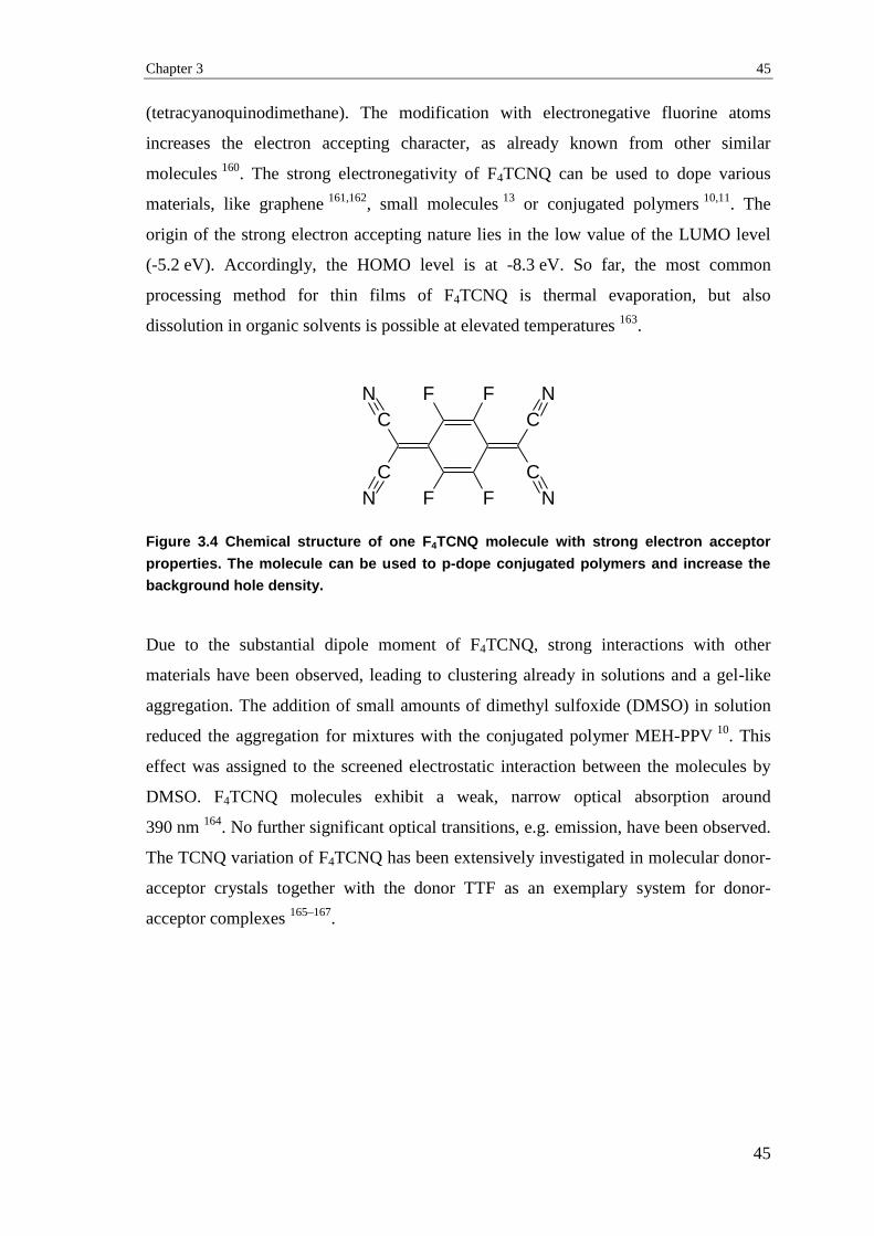
Chapter 3 45
45
(tetracyanoquinodimethane). The modification with electronegative fluorine atoms
increases the electron accepting character, as already known from other similar
molecules 160
. The strong electronegativity of F4TCNQ can be used to dope various
materials, like graphene 161,162
, small molecules 13
or conjugated polymers 10,11
. The
origin of the strong electron accepting nature lies in the low value of the LUMO level
(-5.2 eV). Accordingly, the HOMO level is at -8.3 eV. So far, the most common
processing method for thin films of F4TCNQ is thermal evaporation, but also
dissolution in organic solvents is possible at elevated temperatures 163
.
F
F F
F
C
C
C
C
N
N N
N
Figure 3.4 Chemical structure of one F4TCNQ molecule with strong electron acceptor
properties. The molecule can be used to p-dope conjugated polymers and increase the
background hole density.
Due to the substantial dipole moment of F4TCNQ, strong interactions with other
materials have been observed, leading to clustering already in solutions and a gel-like
aggregation. The addition of small amounts of dimethyl sulfoxide (DMSO) in solution
reduced the aggregation for mixtures with the conjugated polymer MEH-PPV 10
. This
effect was assigned to the screened electrostatic interaction between the molecules by
DMSO. F4TCNQ molecules exhibit a weak, narrow optical absorption around
390 nm 164
. No further significant optical transitions, e.g. emission, have been observed.
The TCNQ variation of F4TCNQ has been extensively investigated in molecular donor-
acceptor crystals together with the donor TTF as an exemplary system for donor-
acceptor complexes 165–167
.

46
46
3.2 Sample fabrication
3.2.1 Solution preparation
All materials were received as powder and used without further purification. For
processing into thin films, the materials were dissolved in organic solvents
(spectroscopic grade, anhydrous). The solutions were stirred for several days on a
hotplate. All vials were closed with a sealed cap and Parafilm© to minimize solvent
evaporation, which would lead to changes in the solution concentration.
3.2.2 Spin-Coating
Thin films (~100nm) of organic semiconductor on various substrates were prepared
using the spin-coating technique. The substrates were chosen based on the transmission
properties required for the respective experiments. Most optical experiments were either
conducted with round quartz substrates (Ø20mm, Hereaus, Suprasil) or rectangular
coverslips (15mmx15mm, Menzel-Gläser, #5). CaF2 substrates were used for transient
absorption measurements with probe energies in the mid-IR. For SEM measurements,
silicon wafers without thermal oxide were cut to obtain substrates of about
10 mm x 10 mm size. Before film deposition, all substrates were cleaned in an
ultrasonic bath for at least 10 minutes in acetone and isopropanol. Afterwards, the
substrates were washed once more with acetone and isopropanol and blown dry in a
nitrogen stream.
The spin-coating process consists of four steps. First, a substrate is fixed on a vacuum
holder. Next, a small amount of solution is dropped on the substrate with a pipette.
Depending on the substrate size, 50-100 µl of solution was used. The substrate is set
into rotation, thereby hurling away most of the solution until only a thin film is left.
Under these conditions, the solvent evaporates fast, leaving a homogeneous thin film of
material deposited on the substrate. Rotation speeds had to be adapted for the different
solvents and were between 1000 and 3000 RPM with a spinning time of 30-60 s.
3.2.3 Doctor-blading
For the preparation of doctor-bladed samples a homebuilt doctor-blader was used. The
basic setup is shown in Figure 3.5. A blade with a sharp, straight edge is placed less one

Chapter 3 47
47
millimeter above the substrate. The blade edge has to be parallel to the substrate surface
to avoid any unwanted variations of film thickness over the substrate length.
Figure 3.5 Scheme of the doctor-blading setup. The substrate is shown in grey, the
organic semiconductor solution in green and the blade is white with black border. The
arrow indicates the movement of the blade, which is spreading out the solution on the
substrate.
With a pipette a small amount of solution (~5-10 µl) was placed on the substrate close
to one side of the blade. By moving the blade over the substrate with a motorized stage
(Thorlabs MTS50/m-Z8 with TDC 001) the solution was spread homogeneously,
creating a thin film of solution. A slow blade speed (0.5 mm/s) was chosen to allow
instantaneous drying of the thin solution film behind the blade. The blade movement
was stopped before the edge of the substrate and residual solution was removed with a
dust free wipe. The blade was cleaned after each run to avoid any cross contamination.
The doctor-blading technique allows creating thin (~100 nm) homogeneous films on
substrates with various dimensions, which was a requirement for our SEM sample size
of 10 mm x 10 mm.
3.2.4 Solar cell fabrication
Solar cells are prepared from solution on glass substrates. A scheme of the cell
geometry is shown in Figure 3.6. ITO coated float-glass substrates were bought from
Präzisions Glas & Optik GmbH (CEC010S, 15 mm x 15 mm, sheet resistance
≤ 10Ω/sq.) and used as received. A two millimetres strip of ITO was etched away with
HCl (37%) and zinc powder. Afterwards, the substrates were sonicated in distilled
water, acetone and isopropanol for 10 min each. Finally, the substrates were cleaned for
5 min in oxygen plasma to remove any organic residue. In the next step, a PEDOT:PSS
layer was spin-coated in ambient conditions and dried at 150 °C for 10 min. After

48
48
transfer to a nitrogen filled glovebox the active layer was spin-coated onto the samples
from organic solvent solution. In the last step, aluminium electrodes were evaporated.
Figure 3.6 Sketch of the solar cell geometry. A PEDOT:PSS layer is spin-coated on an ITO
patterned glass substrate. The polymer:fullerene blend is spin-coated on top of the
annealed PEDOT:PSS layer. In the last step, aluminium electrodes are evaporated.
The setup for thermal evaporation of the electrodes was integrated in a nitrogen glove
box (MBraun 20G) and consisted of a vacuum bell (Leybold Glocke 300), a turbo-pump
to evacuate the bell (Leybold Turbotronik NT 20) and a power supply (Leybold AS 053).
The samples were placed in a sample holder and covered with a mask featuring the
pattern of the electrodes. A tungsten boat was mounted between two electrodes inside
the bell and filled with the evaporation material. In the case of aluminium several small
tungsten pieces were added to prevent a current overshoot when the aluminium starts to
melt. The sample holder was placed in the bell and a vacuum of at least
5x10⁻⁶
mbar was generated. The current on the power supply was increased until the
material starts to melt and a constant evaporation rate was reached. To deposit the
material on the samples, a shutter above the tungsten boat was opened. The thickness of
the deposited layer was monitored with an oscillating crystal microbalance. Once the
desired thickness was reached, the shutter was closed. The current was reduced to zero
and the pressure in the bell was increased to atmospheric pressure.

Chapter 3 49
49
3.3 Experimental setups
3.3.1 Steady state spectroscopy
3.3.1.1 Absorption spectroscopy
The energies of optical transitions from the ground level (Paragraph 2.5) can be
determined by measuring the loss in light transmission through a diluted solution or thin
film samples. Such spectroscopic absorption measurements were performed with a
Varian Cary 5000 UV-NIR spectrometer in the range from 200 nm to 3300 nm. The
basic principle of the setup is detailed in (Figure 3.7).
Figure 3.7 Schematic principle of absorption spectroscopy. Monochromatic light is
generated by a dispersive element and passed through the sample. The change in
transmission, induced by the sample, is measured wavelength dependent with a
photodetector.
A strong light source creates white light with a broad spectral distribution from which a
selected wavelength is isolated with a monochromator. The monochromatic light is
passed through the sample and the intensity in front and behind the sample is measured
with a photodiode detector. The wavelength dependent absorbance A(λ) is defined as
( ) (
( )
( )) (3-1)

50
50
where I0(λ) is the light intensity in front, and I(λ) behind the sample. Under the
assumption that scattering can be neglected for clear films, the absorbance is a measure
for the number of photons absorbed in the sample.
Experimentally, the monochromatic beam was split into two beams with a beam splitter
in the spectrometer. One beam was passed through the sample and gives a measure for
I(λ), while the other one was used as a reference and gives I0(λ). The correction for
substrate induced changes in the transmission spectrum, e.g. reflection or absorption,
was performed by measuring a blank substrate to obtain a baseline. This correction was
then automatically subtracted from the sample spectrum in the instrument software.
3.3.1.2 Photoluminescence spectroscopy
In photoluminescence spectroscopy optical transitions are induced by an external
monochromatic light source tuned to the absorption region of the sample (Figure 3.8).
The emitted light from the excitations is passed through a dispersive element and the
intensity is measured with a detector.
Figure 3.8 Schematic principle of photoluminescence spectroscopy. The sample is
excited by monochromatic light and the emitted light is detected spectrally resolved with
a photodetector.
Steady state photoluminescence measurements were performed with a Fluorolog 3
(Horiba Jobin Yvon) spectrometer. For measurements between 300 nm and 1000 nm a
visible double monochromator and a water-cooled photomultiplier tube were used,
while for NIR measurements up to 1600 nm an iHR320 turret monochromator and a
thermo-electrically cooled detector H10330-75 (Hamamatsu) were employed. High
sensitivity measurements were achieved by monitoring fluctuations in the lamp intensity

Chapter 3 51
51
with a reference photodiode. All measurements were corrected for the quantum
efficiency of the detectors.
3.3.1.3 Steady-state photo-induced absorption (PIA) spectroscopy
Steady-state PIA is employed to detect the population of photo-induced states in thin
organic semiconductor films or solutions. The schematic setup of this experiment is
shown in Figure 3.9.
Figure 3.9 Schematic representation of steady-state PIA experiments used to study
photo-induced states in organic semiconductor films. The transmission through the
sample of a steady state white light (WL) source (e.g. a halogen lamp) is detected with
and without excitation by a continuous-wave (cw) laser. The change in transmission is a
measure for the photo-induced states. Spectral resolution is obtained by dispersing the
WL in a monochromator before detection.
A continuous-wave (cw) laser is used to photo-induce states in the sample, e.g. polarons
or triplets. The transmission of a steady-state white light (WL) source through the
sample is detected with and without laser excitation. The photo-induced states will lead
to additional absorption, hence, reduce the transmission. The relative change in
transmission T of the probe WL with/without pump laser is proportional to the density
of photo-induced states n:
(3-2)
In this equation, d stands for the film thickness and α is the absorption coefficient of the
investigated states at the probe wavelength. The WL is dispersed by a monochromator

52
52
and afterwards detected with a photodiode. The steady-state pump laser is modulated
with a chopper at a low frequency (<250 Hz). Therefore, also the laser-induced change
in transmission ΔT is modulated with this frequency. The value for ΔT is directly
obtained by analysing the signal of the photodiode with a Lock-In set to the modulation
frequency. The transmission T is determined by measuring the white light spectrum in a
second experiment without laser excitation.
3.3.2 Time resolved spectroscopy
3.3.2.1 Femtosecond laser systems
The core of the laser system is the regenerative amplifier system (RegA 9000, Coherent)
used to amplify laser pulses from a mode-locked Titanium:sapphire oscillator (Vitesse
2W, Coherent). A compressor unit behind the RegA 9000 generates ~70 fs laser pulses
at around 800 nm wavelength. These pulses are used in optical parametric amplifiers to
generate ultra-short laser pulses in the visible to mid infrared energy region. Figure 3.10
gives an overview of the general outlay of the system.
Figure 3.10 Schematic overview of the regenerative amplifier system used to generate
femtosecond laser pulses. Femtosecond pulses from a Ti:Sapphire oscillator source are
amplified in a Coherent RegA 9000 pumped by a Coherent Verdi cw-laser.
The Vitesse laser system is pumped by a solid state steady-state Nd-YVO4 laser (Verdi
2W, Coherent) at 532 nm and generates sub-100 femtosecond laser pulses at 800 nm
centre wavelength with a repetition rate of 80 MHz and 5 nJ pulse energy, using Kerr-

Chapter 3 53
53
Lens mode-locking. The negative dispersion mirrors in the cavity provide the dispersion
compensation needed to produce sub-100 femtosecond pulses.
The pulses from the Vitesse are temporally stretched with a multi-pass holographic
grating before entering the RegA 9000. This allows for efficient amplification of the
pulses, since during the longer pulse duration more power can be injected from the
pump laser (Verdi V-10, Coherent). Additionally, lower peak fluences occur in the
RegA 9000 preventing damage to optical components. A Q-switch keeps the resonator
just below lasing threshold, leading to a build-up of energy stored in the
titanium:sapphire crystal. One pulse from the Vitesse seed laser is fed into the resonator
through a Faraday isolator using an acousto-optic cavity dumper. At the set repetition
rate of 90 kHz every 888th
pulse from the Vitesse gets coupled in. The Q-switch is
turned off and the strong occupation inversion amplifies the individual pulses during 20
to 30 roundtrips in the cavity. The amplified pulses are out-coupled using the cavity
dumper. They pass through the Faraday-isolator and are separated from the seed-pulses
with polarization filters. Afterwards, they are compressed down to about 70 fs pulse
duration in the compressor unit. Pulse lengths after amplification were checked with a
real-time autocorrelator (Pulse Scope, APE). In summary, the RegA system generates
~70 fs pulses with a centre wavelength of 800 nm and average power of 6 µJ per pulse
at a repetition rate of 90 kHz.
3.3.2.2 Optical parametric amplifier (OPA)
The femtosecond laser system gives pulses with ~70 fs pulse duration and a wavelength
around 800 nm. In order to tune the energy of the pulses according to the absorption
spectrum of the investigated materials in the visible energy range, an optical parametric
amplifier (OPA) from Coherent (OPA 9400) was used. Figure 3.11 shows the general
outlay of the setup.

54
54
Figure 3.11 Schematic overview of the Coherent OPA 9400 optical parametric amplifier
used for tuning the energy of femtosecond laser pulses in the visible range. White light
seed and 400 nm pump pules from second harmonic generation (SHG) are superimposed
on a non-linear crystal. A narrow part of the white light spectrum gets amplified by hitting
the crystal under the corresponding phase matching angle.
The 800 nm RegA output is split into two parts, with 75 % of the signal send to a BBO
crystal for second harmonic generation to produce 400 nm pulses (SHG). The remaining
25 % are focused into a sapphire crystal which produces a white light continuum from
450 nm to 1500 nm due to self-phase modulation. A small part of the WL is outcoupled
from the OPA through a semi-transparent mirror. The remaining WL passes through a
first delay stage, so that the optical path lengths of WL and SHG match when arriving at
the non-linear OPA crystal (BBO material) for parametric amplification. Mirrors are
used to collimate the SHG and WL beam and superimpose them on the OPA crystal.
After the first pass, the SHG and amplified WL component are split and the SHG is
send through a second optical delay stage. Afterwards, the beams pass through the OPA
crystal for a second amplification. After the second pass the signal, idler and the
remnant pump beam exit the OPA. The signal wavelength can be tuned from 500 nm to
700 nm, while the idler wavelengths are between 940 nm and 2400 nm.
3.3.2.3 Non-linear optical parametric amplifier (NOPA)
Measurements of the polaron intraband absorption in the mid-infrared avoid interfering
signals from superimposed triplet absorption in the near-infrared. We therefore aim to

Chapter 3 55
55
probe the polaron signal with ultra-short laser pulses in this spectral region. A two stage
non-collinear optical parametric amplifier (NOPA Ultimate, MRX Clark) is used to
generate laser pulses in the near-IR range from 950 nm to 1580 nm (signal) and the mid-
IR from 1620 nm to 4800 nm (idler). Figure 3.12 gives an overview on the NOPA
geometry.
Figure 3.12 Schematic overview of the non-collinear optical parametric amplifier used for
tuning the energy of the femtosecond laser in the infrared spectral region. Wavelength
selective amplification is achieved by two consecutive amplification stages consisting of
non-linear crystals (BBO, LiNbO3). Near-IR pulses generated from white light
amplification in the first stage seed the second stage. The first stage is pumped by
400 nm laser pulses while the second stage uses an 800 nm pump.
The output from a RegA 9000 laser system is coupled into the NOPA. One part of the
signal is doubled in frequency to 400 nm with second harmonic generation (SHG). With
the other part, a white light (WL) super-continuum is generated by self-phase
modulation. WL in the visible range is created with a sapphire plate, while for the
infrared range an yttrium aluminium garnet (YAG) plate is placed. On the first OPA
crystal (BBO) the SHG signal and the WL are superimposed. To reach pulse energies in
the mid-infrared around 3000 nm, the first stage has to be tuned to wavelengths in the
near-infrared around 1100 nm. Due to the chirped nature of the WL continuum the
amplification wavelength can be tuned by changing the temporal delay between SHG
and WL pulses. The phase matching angle is adjusted accordingly by tilting the OPA
crystal. In the second stage, NIR pulses from the first stage are superimposed with the

56
56
800 nm pulses from the RegA 9000 on a LiNbO3 crystal to generate parametric
amplification. The idler of the second stage gives ultra-short mid-IR pulses according to
formula (3-3).
(3-3)
3.3.2.4 Time resolved photoluminescence
For time resolved photoluminescence experiments a femtosecond laser system was used
to excite the sample with ultra-short laser pulses (~100 fs). The emission from the
sample was spectrally dissolved in a spectrograph and hit the entrance slit of the streak
camera. A streak camera (Hamamatsu C5680, synchroscan unit M5675) with a
measurement range up to 2.2 ns and a maximum resolution of 5 ps was used. The streak
tube N5716-03 was used for measurements in the spectral range from 400 nm up to
900 nm. For measurements in the IR above 900 nm one had to change to a streak
camera with tube N5716-02. Figure 3.13 shows the basic operating principle of a streak
camera. In a first step the photons are multiplied with a photomultiplier and converted
into electrons at the photocathode. The time resolution is achieved by sending these
electrons through two deflecting electrodes in parallel capacitor configuration. A linear
increasing voltage sweep is applied between the plates, initialized by a trigger
synchronized to the laser pulse. The first electrons arriving at the capacitor experience
only a low voltage and are therefore barely deflected. Electrons arriving later are
exposed to a higher voltage and accordingly experience a stronger deflection. This leads
to a vertical spread of the electrons. Before reaching the CCD camera, the electrons are
amplified in a micro-channel plate and re-converted into photons on a phosphor screen.

Chapter 3 57
57
Figure 3.13 Schematic geometry and working principle of a streak camera. Photons
excited in a sample with an ultra-short laser pulse are passed through a deflection unit
which allows temporally resolved detection.
An exemplary picture on the CCD camera is shown in (Figure 3.14). On the x-axis the
signal is spectrally resolved, where temporal resolution is given on the y-axis. The
colour coding represents high (red) and low (black) intensities.
Figure 3.14 Example of a streak camera measurement. Emission from a PCPDTBT thin
film excited at 400 nm; emission centre at 835 nm; full vertical dimension of the picture
corresponds to 300 ps time range.
3.3.2.5 Pump-probe technique
With the pump-probe technique photo-induced proceses are investigated on an ultra-fast
time scale. A femtosecond (fs) “pump” laser pulse excites the sample and creates new

58
58
states, e.g. triplets or polarons. A second “probe” laser pulse arrives time delayed with
respect to the pump pulse and is absorbed by the photo-induced states, i.e. the states
created by the pump pulse. The ratio of transmission ΔT/T of the probe pulse
with/without pump pulse is proportional to the density of photo-induced states n
(Equation (3-2)). In the present setup the pump pulses were either the signal from an
OPA in the range 500-700 nm or the frequency doubled direct output (400 nm) from the
RegA. As probe pulses, either the while light continuum generated in the OPA (500-
1500 nm) or the output of the NOPA (1100 nm – 5000 nm) was used. All laser pulses
had the frequency of the amplifier system (90 kHz).
Figure 3.15 Schematic representation of the pump-probe setup used to study photo-
induced states in organic semiconductor films. The difference in transmission of a probe
pulse through the sample is detected with and without pump pulse. Temporal resolution
is achieved by changing the time delay between pump and probe pulses with a delay
stage.
For measurements in the mid-IR, using the idler of the NOPA as probe, a germanium
plate was placed in front of sample and detector to block photons with undesired
energies, i.e. the signal pulses from the NOPA. On the other hand, using the WL pulses
from the OPA as probe, interference filters (Melles Griot CVI) with the respective
energy pass were placed in front of the photodiode to detect at the desired energy.
For probe energies above 1.24 eV a high speed silicon photodiode (Thorlabs DET 210)
was used. For energies between 1.24 eV and 0.73 eV a high-speed InGaAs detector
(Thorlabs, DET 410) and for the measurements with mid-IR pulses around 0.4 eV a
nitrogen cooled MCT detector (Infrared Associates, MCT-5-N-2.0) were employed.

Chapter 3 59
59
The on/off frequency of the pump pulse was modulated with a mechanical chopper at
6 kHz, which leads to an averaging of 15 probe pulses during one on/off phase. To
increase the signal to noise ratio, the signal from the photo-diodes was measured with
lock-in detection. Before entering the Lock-Ins (Stanford Research SR830), a pre-
amplifier (Stanford Research, SR560) enhanced the signal. A first lock-in was set to
90 kHz, which is the repetition rate of the probe beam. With this Lock-In the
unmodulated transmission through the sample was detected. The output of the first
Lock-In was then fed into a second Lock-In, which was set to 6 kHz, i.e. the modulation
frequency of the pump beam. Hence, the output of the second Lock-In provides the
change in transmission induced by the pump pulse. The ratio of the signals measured at
the second (change in transmission) and the first (transmission) Lock-In gives the
relative change in transmission ΔT/T, which is a measure for the number of photo-
induced states as shown in Equation (3-3). The samples were placed in a homebuilt
cryostat with CaF2 windows and evacuated with a turbo pump (Pfeiffer Vacuum, TSH
071 E) to pressures below 10-5
mbar to keep them under inert conditions. Temporal
resolution is achieved by delaying the pump pulse with respect to the probe pulse, using
a translation stage (Aerotech ATS100). The maximal delay between pump and probe is
limited to 1 ns by the length of the stage (0.3 m). For all measurements, any beam walk
due to inaccurate coupling to the translation stage was avoided by monitoring the beam
on a beam profiler (Data Ray Inc., WinCamD). The beam profiler was also used to
check the beam diameters in order to keep the probe beam much smaller than the pump.
This assures homogeneous excitation over the whole probe beam area. Beam fluences
were kept as low as possible (<5 µJ/cm²) to avoid any non-linear effects and to be as
close to solar cell operation conditions as possible.
3.3.3 Film morphology characterization
3.3.3.1 Scanning electron microscopy (SEM)
In scanning electron microscopy (SEM) an electron beam is used to investigate the
surface morphology and properties of samples. We used a Zeiss Ultra Plus at 750 V
acceleration voltage. The SE2 detector mainly detects secondary electrons, which give
insights about the topography of the sample surface. On the other hand, the In-Lens
detector detects secondary electrons, but uses a charged pole piece to suck electrons
leaving the sample to the detector. This gives the In-Lens detector a higher sensitivity to

60
60
variations in the electronic and material properties of the sample. The working distance
was kept at 3.5 mm to ensure high collection efficiencies of secondary electrons aided
by the electrostatic lens and allowing efficient detection of SE2 electrons at the same
time. For details of SEM measurements the reader is referred to the seminal
literature 168,169
.
3.3.3.2 Transmission electron microscopy (TEM)
In transmission electron microscopy (TEM) the transmission of a focussed electron
beam through a sample is measured. Images were taken with a JEOL transmission
electron microscope operated at 80 kV. The use of an electron beam as imaging tool
allows for very high spatial resolution. It is possible to measure small differences in
electron transmission as required to map the composition of organic semiconductor
blends, where the constituting materials differ only slightly in chemical composition. In
order to apply this technique the thin organic semiconductor film was transferred on a
carbon grid as support. For this, the film has been spin-coated onto a PEDOT:PSS
coated substrate. By gently sliding the substrate into a water filled beaker, the water-
soluble PEDOT:PSS is dissolved and the film floats on the water surface. From there it
was picked up with the carbon grid.
3.3.3.3 Atomic force microscopy (AFM)
For mapping the topography of samples an atomic force microscope (Veeco, Innova
scanning probe microscope) was used. Due to the soft nature of organic
semiconductors, measurements were taken in tapping mode to avoid modifications of
the surface during acquisition. A cantilever was set into periodic vertical oscillations
and approached to the film surface, while the oscillation was monitored by the
deflection of a laser beam from the cantilever. The forces from the sample acting on the
cantilever, e.g. Van der Waals or electrostatic interactions, change the amplitude of the
oscillation. By moving the cantilever up and down to maintain the initial amplitude of
oscillation, a height profile of the sample surface was obtained.
3.3.3.4 Confocal laser scanning microscopy
For mapping of the photoluminescence from thin film samples, a laser scanning
confocal microscope was used. In order to obtain the best possible resolution,
immersion oil was used. Resolutions around 300 nm have been achieved. A laser beam

Chapter 3 61
61
from a continuous wave laser (Laser Quantum Opus with stabilized MCP6000 power
supply) with a wavelength of 532 nm was coupled into a standard confocal microscope
(Olympus IX81 FVSF-2). A 100x objective (UPLANFL N 100x) focussed the laser on
the sample surface, which was translated in three dimensions. The emitted
photoluminescence from the sample was collected through the excitation optics and
detected with a photodiode. A long-pass colour filter was used to block the excitation
beam. Spatial resolution in the sample plane was achieved with a deflection unit
consisting of two mirrors placed at 90 degrees to each other. By moving the mirrors a
two dimensional area of the sample was scanned with the focussed laser beam. By
correlating the position of the laser beam with the detected photoluminescence intensity
a 2D map of the photoluminescence was obtained.


63
63
4 Low-voltage Scanning Electron Microscopy
Imaging of Doped Organic Semiconductors Films
In this chapter, a simple and fast method to unravel dopant distributions in thin films of
conjugated polymers (PCPDTBT, P3HT) is presented. In addition, by performing a
systematic study as a function of dopant concentration, the role of dopant molecules on
polymer film nanomorphology is investigated. First, we study changes in film
topography of organic semiconductor polymers in the pristine form and in the presence
of the dopant F4TCNQ by atomic force microscopy (AFM). Further, low-voltage
scanning electron microscopy (SEM) is employed to monitor the surface morphology
and material composition of doped films. Regions with increased contrast are detected
in doped films. Photoluminescence (PL) mapping in the plane of the film is used to
assign these distributions to dopant rich and dopant deficient domains. Our experiments
show that dopant distributions can be detected as a difference in SEM contrast,
originating from site-sensitive surface charging by the electron beam. In summary, we
demonstrate low-voltage SEM as a convenient tool to monitor F4TCNQ distributions
and clustering thresholds in different conjugated polymers.

64
64
4.1 Motivation for dopant distribution mapping in polymeric
organic semiconductors
A prerequisite for the success of organic electronics in the current information-
technology market is performance and reliability. Recent scientific efforts towards this
milestone consider the use of dopant molecules to improve the transport characteristics
of light emitting diodes and solar cells 170–173
. Doping has been demonstrated to be
critical in tuning the injection properties at metal-semiconductor interfaces, leading to
full control over device parameters 174–176
. Spatial control of the dopant molecules’
position has the potential to improve charge injection by placing dopants near the
contacts 175,177
. Positioning of dopants in transport layers improves carrier
drift/diffusion 178
and also charge separation at heterojunctions 179
. While in devices
based on small molecules spatial control can be easily achieved by sequential
evaporation of layers to form stacked devices 170
, this aspect remains challenging for
solution processable conjugated polymers. However, also for these materials there is
substantial interest in achieving control of electronic processes by doping 11,180
.
Recently, the physical origin of the doping mechanism has seen a renewed interest,
partially because of the demonstration of single-dopant molecule imaging by scanning
tunnelling microscopy (STM) 12
and the description of hybrid states at the
dopant/semiconductor interface 181,182
. Systematic studies, as a function of the
dopant/semiconductor weight ratio, report changes in electrical characteristics, often
showing a saturation in mobility and conductivity as the ratio is increased over a certain
threshold 11,183
.
A critical aspect is the dopant distribution within the semiconductor and the effect of
dopant molecules on the organic semiconductor morphology. The latter issue is
expected to be highly relevant, considering the widely reported and discussed effects of
meso-morphology on the optoelectronic characteristics of organic semiconductors 184
.
On the other hand, the nature of the intermolecular interactions influences the dopant
distribution on the nanoscale. In this respect, the experiments of Kahn and co-workers
by STM 12
are extremely valuable. In these experiments, single dopant molecules were
placed in highly ordered organic semiconductor molecule films of only a few molecular
layers. The effect of this placement on the charge distribution around the individual
dopant molecules was studied. However, such a method is limited to ultra-thin films
exhibiting high crystallinity. Thus, it remains a great challenge for amorphous polymer-

Chapter 4 65
65
dopant blends to observe dopant distributions on the molecular level. Homogeneous
dispersion of dopant molecules in the host material is highly beneficial to maximize the
wavefunction overlap for electron or hole donation 185
, while clusters might reduce
doping efficiencies. A tool to monitor these phenomena in solution processable
disordered polymeric semiconductors, where films are often deposited as
polymer/dopant blends, is lacking.
We studied the morphology of two exemplary conjugated polymers, PCPDTBT
(poly[2,1,3-benzothiadiazole-4,7-diyl[4,4-bis(2-ethylhexyl)-4H-cyclopenta[2,1-b:3,4-b']
dithio-phene-2,6-diyl]]) and P3HT (poly(3-hexylthiophene), doped at different
concentrations with the small molecule F4TCNQ (2,3,5,6-Tetrafluoro-7,7,8,8-
tetracyanoquinodimethane). These polymers are known to be benchmark systems for
solar cells and field effect transistors, respectively. The materials were obtained from
1-material (PCPDTBT), and Sigma-Aldrich (P3HT, F4TCNQ). Both polymers had a
similar molecular weight of about 20.000 g/mol. Since PCPDTBT and P3HT are well
known hole transporting materials they were doped with the strong electron acceptor
F4TCNQ. Addition of the dopant to the polymer films leads to ground state charge
transfer and generation of holes in the polymer HOMO (see Paragraph 5.3 for a detailed
discussion). In the following, we present SEM imaging as a method to correlate
differences in image contrast to dopant rich and dopant deficient regions. This technique
allows us to study the effects of dopant molecules on film morphology and find the
critical concentrations for dopant clustering or self-segregation.
4.2 Morphological investigation of doped conjugated polymer
films with AFM and SEM
In this paragraph we study the surface morphology of doped conjugated polymer films
with AFM and SEM. Films with different levels of doping up to 10% were investigated.
We chose the low-bandgap polymer PCPDTBT and the well-known polymer P3HT as
exemplary compounds. The dopant F4TCNQ was added to the polymer in solution. All
doping ratios are given per weight of the polymer.
First, AFM is used to study the film topography. Figure 4.1(a-d) show AFM images of
PCPDTBT films doped at different weight ratios with F4TCNQ. The topography of the
undoped films is reasonably flat with maximum elevations of 12 nm. A fibrous meso-
structure is visible in pristine PCPDTBT films (Figure 4.1a). An equally flat topography
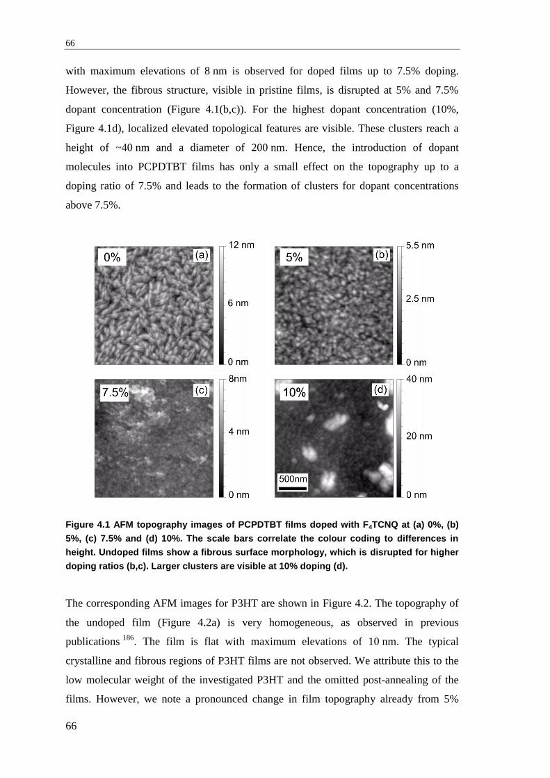
66
66
with maximum elevations of 8 nm is observed for doped films up to 7.5% doping.
However, the fibrous structure, visible in pristine films, is disrupted at 5% and 7.5%
dopant concentration (Figure 4.1(b,c)). For the highest dopant concentration (10%,
Figure 4.1d), localized elevated topological features are visible. These clusters reach a
height of ~40 nm and a diameter of 200 nm. Hence, the introduction of dopant
molecules into PCPDTBT films has only a small effect on the topography up to a
doping ratio of 7.5% and leads to the formation of clusters for dopant concentrations
above 7.5%.
Figure 4.1 AFM topography images of PCPDTBT films doped with F4TCNQ at (a) 0%, (b)
5%, (c) 7.5% and (d) 10%. The scale bars correlate the colour coding to differences in
height. Undoped films show a fibrous surface morphology, which is disrupted for higher
doping ratios (b,c). Larger clusters are visible at 10% doping (d).
The corresponding AFM images for P3HT are shown in Figure 4.2. The topography of
the undoped film (Figure 4.2a) is very homogeneous, as observed in previous
publications 186
. The film is flat with maximum elevations of 10 nm. The typical
crystalline and fibrous regions of P3HT films are not observed. We attribute this to the
low molecular weight of the investigated P3HT and the omitted post-annealing of the
films. However, we note a pronounced change in film topography already from 5%

Chapter 4 67
67
doping on. For the doped films, the roughness increases and elevations of ~50 nm
height are present. The films also show a coarser morphology compared to the undoped
films with the formation of larger domains. This effect increases with the formation of
clusters at 7.5 and 10%. Thus, the introduction of dopant molecules has a greater effect
on P3HT films with respect to PCPDTBT films and leads to the formation of a more
disordered film topography. At high doping ratios (10%) the formation of clusters is
observed in both polymers.
Figure 4.2 AFM topography images of P3HT films doped with F4TCNQ at (a) 0%, (b) 5%,
(c) 7.5% and (d) 10%. The scale bars correlate the colour coding to differences in height.
Undoped films show a homogenous, flat surface morphology. The film roughness
increases for higher doping ratios (b-d).
The AFM experiments give information on changes in film topography due to
incorporation of dopant molecules. However, the detailed distribution of dopant
molecules in the films cannot be resolved. Additionally, the origin and composition of
the aggregates and clusters at higher doping cannot be analysed. For this we need to
employ a technique which is sensitive to differences in material properties. Scanning
electron microscopy (SEM) uses differences in electron yield to image samples. Since
the electron yield depends on the investigated materials’ elementary and electronic

68
68
properties, SEM can be used to study the material composition of samples. Therefore
we use SEM in the following section to investigate the dopant distribution in doped
polymer films.
Figure 4.3(a-h) shows low acceleration voltage (0.75 kV) SEM images of PCPDTBT
thin films (100±10 nm thickness) doped at different concentrations with F4TCNQ. The
films are deposited on a silicon substrate (without oxide layer) by doctor-blading and
loaded in the SEM chamber without any further pre-treatment. The SEM data is shown
in two rows: In the top row, the In-lens detector positioned within the electron column
of the microscope was used, whereas in the bottom row, images were detected with a
detector for secondary electrons (SE2). The SE2 detector renders mainly the surface
morphology, while the information provided by the In-lens detector is more sensitive to
material properties, such as the elements’ atomic number 168
.
Figure 4.3 Scanning electron microscopy images of PCPDTBT doped at different ratios
with F4TCNQ as stated. Images taken with InLens (a-d) and SE2 (e-h) detectors.
Acceleration voltage for all images was 0.75 kV. The undoped films (a,e) show a fibrous
morphology which is reduced for higher doping ratios (b-d, f-h). Regions with increased
contrast are visible at high doping ratios in the InLens image (d). The scale bar gives the
dimensions for all images.
Figure 4.3(a,e) show the pristine polymer film surface morphology, exhibiting a fibrous
texture with dimensions on the order of a few tens of nanometres. No further ordering
on a larger length scale is observed in Fourier transformations of the images. This
observation correlates with the pristine film topography obtained from AFM images

Chapter 4 69
69
(Figure 4.1a). From previous work, PCPDTBT is known to be a semi-crystalline
polymer 187
. Under slow deposition conditions, as chosen here, the polymer chains are
expected to order into crystalline domains, detected by the SE2 detector as small fibres.
From the much higher length of the fibres with respect to the polymer chain length, it is
reasonable to assume that the polymer chains are aligned across the diameter of the
fibres and not extended along the whole fibre. Remarkably, the fibrous structure is also
visible in the InLens picture. This indicates a difference in electron yield between the
fibrous and amorphous regions, not related to topography. Differences in electron yield
originate from differences in the electron densities. Therefore, the observation of the
fibrous domains in InLens images points to different electron densities in fibrous and
amorphous regions. We attribute these differences in electron density to a higher
molecular packing in the fibrous regions.
Notably, the pristine surface morphology is disrupted in doped films for doping ratios of
5% and 7.5% (Figure 4.3(b,c,f,g)). The amount of fibres substantially decreases and
their size is reduced. At 7.5% doping brighter regions appear which form prominent
clusters at 10% doping (Figure 4.3d,h). We note that these clusters agree in size and
shape with the structures observed in 10% doped films with AFM (Figure 4.1a).
Remarkably, the In-lens image (Figure 4.3d) shows a large contrast between clustered
and amorphous regions. This indicates a difference in electron yield between these
regions and substantial differences in material composition. It is known, that F4TCNQ
molecules in close vicinity to each other are prone to form crystallite clusters due to
their strong intermolecular interactions 10
. As a working hypothesis, we assign the
brighter areas therefore to regions with increased dopant density, i.e. giving rise to
F4TCNQ clusters.
Additionally, we investigated doped films of P3HT to compare our results on
PCPDTBT with another conjugated polymer. Figure 4.4(a-d) show In-Lens SEM
images of P3HT doped at concentrations identical to those used for PCPDTBT. The
morphology of the pristine polymer is substantially less structured compared to
PCPDTBT, which indicates a lower extent of ordering and less interchain interactions.
Accordingly, pristine P3HT films have a more homogeneous morphology compared to
PCPDTBT. Further, an increase in image contrast develops already at low doping ratios
(5%, 7.5%) and noticeable areas of increased brightness are observed (Figure 4.4(b,c)).
As for doped PCPDTBT, we propose that these domains are dopant rich. At 10%

70
70
doping, the dopant clusters reach diameters up to 500 nm, as shown in Figure 4.4d. The
fact that the image of the 5% doped sample exhibits larger bright areas compared to
higher doped films is due to the relative contrast of the images. Already during image
acquisition, the contrast range of each picture is adjusted to the brightest and darkest
region of the image (“auto-contrast”). Accordingly, the absolute brightness of the
pictures cannot be directly compared and the presumably larger area of bright regions in
the 5% film, with respect to the 10% one, is due to a difference in image contrast scale.
Figure 4.4 Scanning electron microscopy images of P3HT doped at different ratios with
F4TCNQ as stated. Images taken with InLens (a-d) and SE2 (e-h) detectors. Acceleration
voltage for all images was 0.75 kV. Undoped films (a,e) show a homogenous morphology.
Regions of increased contrast are visible in doped films (b-d) with the contrast
increasing with doping. At higher doping ratios (g,h) bright features in InLens pictures
relate to features in SE2 topography images (white outlines).The SE2 pictures show a
concomitant increase in film roughness. Scale bar gives dimensions for all images.
The lower row in Figure 4.4(e-h) presents images taken with an SE2 detector sensitive
to topography. While the undoped film (Figure 4.4a) shows very little surface structure,
already at 5% doping there is a noticeable increase in surface roughness. This correlates
with the observed increase in height distribution in AFM images (Figure 4.2b). At
higher doping ratios it is possible to relate regions with increased height in SE2 images
to regions that appear bright in the InLens pictures (marked regions in Figure 4.4(e-h)).
This effect is in parallel with the cluster formation in highly doped PCPDTDT films.
One could generally expect that a similar increase in SEM image contrast is observed in

Chapter 4 71
71
any polymer-acceptor system and not just in polymer-dopant blends. However, no
comparable increase in SEM contrast is detected in exemplary polymer:fullerene blends
(Appendix A).
In conclusion, the introduction of F4TCNQ dopant molecules into PCPDTBT films
affects the pristine polymer morphology only slightly and leads to phase segregation
only at high doping ratios (10%). On the other hand, for P3HT films, we observe
deviations from the pristine film morphology and phase-segregation already at lower
doping ratios (5%). Brighter and darker regions were observed in SEM images of doped
polymer films, pointing to differences in material properties between these domains. We
proposed that the observed bright regions are dopant rich domains. To assert this
assumption, we investigate the films with photoluminescence (PL) mapping in the next
paragraph.
4.3 Correlation of emission quenching patterns in PL maps
with dopant distributions in SEM images
Another microscopy technique which can give unique insights on the morphology of
organic semiconductors is confocal laser scanning microscopy 188–190
. Confocal
microscopy is particularly suited to probe dopant distributions in our samples, since
dopant molecules induce additional charge carriers in nearby polymers. Therefore, the
PL of these polymers is quenched by exciton-polaron interactions 191
. In our
experiment, a laser exciting the polymer is scanned over the sample plane and the
emitted PL of the polymer is collected point by point, resulting in a 2D PL intensity
map. Figure 4.5 shows the PL imaging of PCPDTBT films undoped (a) and at
increasing concentrations of F4TCNQ (b-d). The full pictures show images which have
been post-processed after acquisition with an imaging processing software for optimal
contrast and intensity, while the insets show the raw data. The post-processing was
necessary because of the substantial decrease in PL intensity with increasing doping
(Figure 4.5, insets). The PL maps of undoped PCPDTBT films (Figure 4.5a) show a
homogenous emission without any patterns. Confocal microscopy has a resolution
comparable to the diffraction limit of the excitation light (~300 nm at the excitation
wavelength of 532 nm). It is therefore not surprising that the fibres observed in SEM
and AFM images for the pristine PCPDTBT sample are not distinguishable. With
increasing doping the overall PL intensity in the PCPDTBT images decreases

72
72
homogeneously in the whole field of view (Figure 4.5(b-d)). This indicates a
homogeneous distribution of dopants in PCPDTBT films with domains much smaller
than 50 nm, which cannot be resolved in the confocal laser scanning microscope.
Accordingly, the homogeneous quenching in doped PCPDTBT films indicates a
homogeneous distribution of dopant molecules in these films.
Figure 4.5 Photoluminescence maps for PCPDTBT (a-d) and P3HT (e-h) thin films doped
with F4TCNQ at different ratios as stated. Images were post-processed for optimal
contrast, while the insets show the raw data. Excitation wavelength was 532 nm
(150 µW). Scale bars give dimensions for all images and insets, respectively.
This observation is corroborated by comparing the PL maps with the SEM images of
Figure 4.3. No bright regions with increased contrast were observed in SEM images of
doped films up to 7.5% doping, which correlates with the homogeneous quenching in
PL maps for these samples. Therefore, our assignment of bright regions in SEM to
dopant rich clusters is supported by PL mapping. Interestingly, clusters, observed with
SEM for the 10% samples, are not observed with the confocal laser scanning
microscope. We attribute this to the almost complete PL quenching for these samples
(Figure 4.5d, inset). Hence, distinguishing dopant induced differences in intensity is not
possible. Summarizing the results for PCPDTBT, the photo-generated excitons, having
a short diffusion length (~20 nm 71
), are quenched with a high probability in the whole
film, indicating a homogeneous dopant distribution in the film up to 7.5% doping.
For the case of P3HT films, undoped samples give rise to homogeneous emission
without any patterns (Figure 4.5e). On the other hand, doped P3HT films

Chapter 4 73
73
(Figure 4.5(e-h)) show modulations in PL intensity already from 5% doping on. The
non-emissive, dark areas increase in size with increasing doping, up to a length scale of
one micron at 10% doping. PL quenching mainly occurs in dopant rich regions, as such,
we can assign darker areas to areas with a high dopant load. Large areas that appear
brighter in Figure 4.6(g,h) are subjected to less exciton-polaron quenching. This leads to
the conclusion, that for P3HT the dopant molecules tend to cluster and not
homogeneously intermix with the polymer molecules from 5% doping on. Shape and
size of the dark areas, i.e. areas of high quenching, are similar to the bright areas
detected in SEM images. This further supports our interpretation of the bright regions in
SEM images to be dopant rich.
It has been shown in previous publications 10,192
, that due to the small dielectric constant
of these materials the electrostatic interaction between the ionized dopant and the
polymer molecules can be substantial. This may create local electric fields which
perturb the assembly of pristine polymer chains. Meanwhile, F4TCNQ molecules have
the tendency to aggregate into crystallites. In our experiments, the minimum amount of
dopant that can be introduced in polymer film without altering the film morphology in
an appreciable way is higher for PCPDTBT (up to 10%) than for P3HT (below 5%).
One possible explanation is the donor-acceptor structure of PCPDTBT which provides
intrinsic on-chain dipoles 193,194
, capable of screening the interaction between the
ionized dopants.
In conclusion, photoluminescence mapping of doped polymer films confirms our
assignment of bright regions in SEM images to dopant rich domains. We present low-
voltage SEM as a new technique to study the in-plane distribution of dopant molecules
in polymeric organic semiconductor thin films with high resolution. The dopant
distribution in two seminal polymers, PCPDTBT and P3HT, was investigated. Doped
P3HT films tend to phase segregate already at 5% and the dopant rich regions reach
diameters up to one micron for 10% doping. On the other hand, films of PCPDTBT
show a homogeneous distribution of dopant molecules up to 7.5% doping. So far, our
results answered the question how dopant distributions can be mapped in amorphous
organic semiconductor films. However, the physical origin of the increased contrast
between dopant and polymer rich domains in SEM images is not yet clear. This
question will be addressed in the next two paragraphs.

74
74
4.4 Monte-Carlo simulation of SEM electron yield from doped
polymer films
Until now, we have not addressed the physical origin of the increased contrast in SEM
images of doped films taken with the InLens detector (Figure 4.3, Figure 4.4). The
observed effect might originate from differences in the materials’ elementary
composition or differences in the electron density. Monte-Carlo simulations were
performed with the Casino 2.0 software to address this question. With the simulation
software the electron yield for a given electron energy and material, as well as the
electron yield from different depths within the sample are simulated. A difference in
atomic number between the investigated materials would lead to differences in the
electron yield, since the electron scattering process involves the interaction between the
accelerated electrons and the investigated elements’ atoms 168,169
. The electron yield
depends accordingly on the mean atomic number of the materials. Figure 4.6 shows the
electron yield distribution as a function of the detected electron energy for the
investigated materials. A film thickness of 100 nm was used in the simulations. The
low-energy secondary electrons are shown as one featureless peak, since the simulation
software is not able to resolve their detailed energy distribution.
Figure 4.6 Monte-Carlo simulation of the electron yield versus energy for P3HT,PCPDTBT
and F4TCNQ. Acceleration voltage was 0.75 kV, film height 100 nm. All materials give
similar yields for secondary and back scattered electrons. The simulation does not allow
resolution of the secondary electron peak, which is shown as a delta peak.

Chapter 4 75
75
All investigated materials show very similar functions of the electron yield with only
minor differences in absolute values. The number of secondary electrons is slightly
increased for P3HT while the backscattered electron yield is slightly higher for
F4TCNQ. Notably, the yield of backscattered electrons compared to secondary electrons
is substantially lower. We rationalize the marginal differences in secondary electron
yields from the negligible difference in the mean atomic number of the organic
molecules’ nuclei. We conclude that the differences in secondary electron yield are too
low to be the underlying reason for the increased contrast in SEM. Additionally, the low
mean atomic numbers of the materials indicate that the contribution of backscattered
electrons in the image formation, either using the InLens or SE2 detector, is minor
compared to inelastically scattered secondary electrons. From the considerations in this
paragraph, a material or chemical contrast can therefore be excluded.
Another explanation for the observed contrast could be the differences in topography, as
shown in the AFM images. For an investigation of these effects, the electron yield
versus film depth was simulated. The plot in Figure 4.7 shows the electron yield against
the depth measured from the film surface.
Figure 4.7 Monte-Carlo simulation of electron yield versus film depth for P3HT, PCPDTBT
and F4TCNQ. Acceleration voltage was 0.75 kV, film thickness 100 nm. P3HT and F4TCNQ
give very similar distributions while the PCPDTBT electron yield extends slightly deeper
into the film.

76
76
The simulations of the electron yield give a similar shape and maximum yield for all
materials. For PCPDTBT some extended gain from deeper regions of the film (about
4 nm) is observed compared to the other materials. However, due to the small overall
penetration depth (ca. 15 nm) of the electron beam in the organic materials at the
applied acceleration voltage of 0.75 kV, this observation is ruled out as the reason for
the contrast increase. Additionally, the penetration depth is much smaller than the
average film thickness of the samples (~ 100 nm). In conclusion, the simulations
underline that differences in the materials’ elementary properties do not explain the
increased contrast observed in SEM InLens images.
4.5 Explanation of contrast increase in SEM images based on
site selective charging of doped films
From the Monte-Carlo simulations in the previous Paragraph 4.4, we excluded a
material contrast as the underlying mechanism for the increased contrast in SEM images
taken with the InLens detector (Figure 4.3, Figure 4.4). Another explanation for the
observed increase in these SEM images might be an interaction of the electron beam
with the sample. Therefore, the following paragraph will discuss the charging of the
sample during electron beam exposure.
Remarkably, we have observed that the increased contrast in SEM images evolves
during image acquisition and is related to a certain exposure time of the samples to the
electron beam. As exemplary samples we show the contrast evolution of undoped (a)
and 5% doped (b) P3HT films in Figure 4.8. During SEM imaging of the pure P3HT
film, it gradually becomes darker with exposure time (Figure 4.8a) without developing
bright regions. This is indicative of a positive charge build-up in the film, leading to a
lower electron yield emerging from the sample surface. On the other hand, bright
patterns evolve with exposure time in doped P3HT films. At intermediate scanning
speeds (Figure 4.8b) an increase in image contrast is observed each time the field of
view is scanned, until the final contrast is reached.

Chapter 4 77
77
Figure 4.8 SEM images for (a) undoped and (b) 5% doped P3HT films taken with the
InLens detector showing the contrast evolution with exposure time. Acceleration voltage
for all images was 0.75 kV. Undoped films show a gradual homogenous darkening, while
regions with increased contrast evolve in doped films.
The gradual darkening of a pure polymer film in SEM indicates that dark regions in the
fully exposed SEM images of doped films are more similar to the pristine polymer, i.e.
dopant deficient. F4TCNQ is known to be a strong p-dopant for organics due to its large
electron affinity and is therefore expected to be negatively charged in close vicinity of a
polymer chain. Thus, we assign the increased contrast of dopant rich domains in SEM
images (Figure 4.3, Figure 4.4) to electron accumulation in the dopant molecules and
enhanced electron scattering by Coulomb repulsion of the incoming electrons during
several scans. We also consider a more probable, beam induced, negative charging of
non-ionized F4TCNQ molecules in clusters, with respect to the polymer. These effects
result in a significantly increased number of electrons backscattered and collected by
the detector from dopant rich regions, giving rise to the contrast enhancement in the In-
lens image.
It is possible to calculate the necessary electron dose for full development of the
contrast by measuring the time until a full exposure of the film is reached. We obtain a
value for the electron exposure per area of 1.6x10⁹/µm
2. It is an interesting question
how this value compares to the number of dopant molecules. The area density of
F4TCNQ molecules is calculated using the mass density of P3HT (1.1 g/cm³) 195
and
F4TCNQ (1.4 g/cm³) 196
together with the film thickness of 100 nm. One obtains values

78
78
for the dopant density of 1.2x10⁵/µm² for a doping ratio of 5%. We note that the dopant
area density is lower than the number of electrons needed for full exposure of the film.
Dopant molecules in clusters are less likely to dope a polymer chain, so that a lower
number of these dopant molecules are negatively charged before exposure to the
electron beam. We assume that the electron beam has a higher charging efficiency on
the pristine F4TCNQ molecules in clusters than charged dopant molecules dispersed in
the polymer film. This leads to the conclusion that not all F4TCNQ molecules will be
equally affected by the electron beam. Identical experiments on doped PCPDTBT films
show a temporal contrast evolution for high doping ratios (10%) when dopant clusters
are observed.
In conclusion, we assign the increased contrast in SEM images of doped polymer films
to a site selective charging of the dopant rich domains.
4.6 Conclusion
We studied the distribution of the small molecule dopant F4TCNQ in the conjugated
polymers P3HT and PCPDTBT. Low-voltage SEM was employed to monitor the
surface morphology of polymeric semiconductor thin films and to characterize the
distribution of dopants in the film at the nanometer scale. It has been shown that the
polymer/dopant blends undergo phase separation at certain dopant concentrations,
resulting in a significant change in film morphology. The critical concentration values
varied for the different investigated polymers. The combination of AFM, SEM and
confocal laser scanning fluorescence microscopy confirm that the clusters appearing at
higher dopant concentrations are dopant rich regions. We identified site-selective
charging of the sample by the electron beam as the underlying mechanism of the
increased SEM contrast. Above the threshold concentration for aggregation, the number
density and size of the dopant rich clusters increased. For the first time, our results
presented SEM as a fast technique for mapping dopant distributions and morphology in
doped conjugated polymer systems. The possibility to study dopant distribution in
amorphous films with SEM is an important result for the fast morphological study of
organic optoelectronic devices with doped layers.

Chapter 5 79
79
5 Reduced charge transfer exciton recombination in
doped organic semiconductor heterojunctions
In this chapter the effect of molecular doping on the recombination of electron-hole
pairs (CT excitons) localized at conjugated polymer:fullerene interfaces is studied. We
demonstrate that doping at low concentrations with p-type dopant molecules reduces
the interfacial recombination via CT excitons and results in a favoured formation of
separated charge carriers. The employed dopant molecules (F4TCNQ) exhibit a strong
electron affinity and are therefore strong electron acceptors. Addition of these p-type
dopants to the polymer in solution facilitates ground state electron transfer from
polymer HOMO to dopant LUMO. Accordingly, the background hole density in the
polymer increases. This leads to a filling of the density of states’ low-energy tail in the
polymer HOMO. We use transient photoluminescence (PL) to reveal a reduced initial
recombination of charge transfer (CT) excitons as a function of increasing dopant
concentration. In addition, probing the generation of separated carriers (polarons) with
mid-infrared (MIR) photo-induced transient absorption (PIA) demonstrates an increase
in polaron density for doping ratios up to 4% weight. The experimental data is fitted
with a rate equation model. The simulations indicate that doping reduces the
probability for CT exciton formation and, by this, enhances polaron generation.
Consistent with the spectroscopic results, we find an increased short circuit current in
solar cells with a doped active layer, which leads to an overall increase in solar cell
performance. We interpret our results based on a reduced formation of emissive charge
transfer excitons in doped blends, induced by state filling of immobile tail states in the
polymer HOMO.

80
80
5.1 Motivation to study the effect of changes in electronic
structure on charge separation
The doping of conjugated polymers has been recently explored to modify the electrical
characteristics of solution processible semiconductors 4,14,197,198
. This work has shown
that background hole density and conductivity can be increased several orders of
magnitude in amorphous organic polymer films. Different amounts of chemical doping
have resulted in increased charge carrier densities, reaching levels sufficient for metallic
conductivity 199
. Similarly interesting, but less investigated is the influence of doping on
optical excitations 200
, as these play a crucial role in the functioning of devices such as
solar cells and light emitting diodes 201
. In pristine polymers several investigations have
clarified that strongly-bound Frenkel excitons, with binding energies of ~0.5 eV 47
, are
the primary photo-excitations in this class of materials 202,203
. As a consequence,
effective charge separation in organic semiconductors preferentially occurs at type II
heterojunctions with a favourable energy offset for exciton dissociation 204
. In general,
the process, leading to fully separated electrons and holes, is thought to be influenced
by an intermediate state, where carriers are localized on two adjacent molecules 94,95,205
.
These localized electron-hole pairs are still bound by a weakened Coulomb interaction
of ~0.2 eV 98
. Such states have been termed CT excitons 95,206
or exciplexes 96,108
and
have recently aroused considerable experimental and theoretical interest 75,101,207
. It
remains a fundamental question whether emissive CT excitons are necessarily
populated for each charge separation event, or if their appearance is entangled with the
electronic characteristics of the materials constituting the heterojunction and the density
of states (DOS) experienced by the photo-excitations. In other words, can
recombination via CT excitons be reduced in favour of charge separation by influencing
the electronic properties of the materials? Doping is known to influence these electrical
characteristics, because of an increased ground-state carrier density and filling of
localized states 192
. Therefore we chose doping as a suitable tool to study the effect of
changes in the electronic structure of the heterojunction on charge separation.
5.2 Preparation of doped PCPDTBT:PCBM blend films
We have focussed our experiments on blends between [6,6]-phenyl C61-butyric acid
methyl ester (PCBM) and the conjugated polymer (Poly[2,1,3-benzothiadiazole-4,7-
diyl[4,4-bis(2-ethylhexyl)-4H-cyclopenta[2,1-b:3,4-b']dithiophene-2,6-diyl]])

Chapter 5 81
81
(PCPDTBT) 120
. PCPDTBT was provided from the group of Prof. Scherf /Universität
Wuppertal) with a molecular weight of 22.000 g/mol. PCBM was purchased from
Nano-C. F4TCNQ was obtained from Sigma-Aldrich. Sketches of the molecular
structures and the energy levels of the investigated materials are displayed in Figure 5.1.
Figure 5.1 Energy level scheme of the investigated materials. The molecular structures of
the materials are shown as insets. The Gaussian broadened polymer HOMO and dopant
LUMO levels, present in disordered films, are drawn. The doping mechanism occurs by a
direct electron transfer from the polymer HOMO to the dopant LUMO, as shown. The
states marked red in the polymer HOMO indicate holes created by the doping
mechanism, while the marked states in the F4TCNQ LUMO relate to transferred electrons.
To achieve effective hole doping of PCPDTBT, we used the small molecule 2,3,5,6-
Tetrafluoro-7,7,8,8-tetracyanoquinodimethane (F4TCNQ), which was added to the
polymer solution before mixing with PCBM. F4TCNQ is known to be an efficient
dopant for conjugated polymers, resulting in p-type doping 10
. This effect is due to the
favourable alignment of polymer HOMO and F4TCNQ LUMO (Figure 5.1), allowing
for direct electron transfer from polymer to dopant. The transfer of electrons generates
positively charges holes in the polymer HOMO. These will fill the immobile tail states
of the HOMO density of states, since these states are lowest in energy. For the
preparation of solutions, chlorobenzene was used as solvent for all samples. First, pure
PCPDTBT and F4TCNQ solutions were prepared. To obtain doped polymer solutions
with a defined doping ratio, the respective amount of F4TCNQ solution was added to

82
82
the pure polymer solution. The dopant-polymer mixture was then added to PCBM
powder to obtain 1:1 (polymer:fullerene) weight ratio blends. Thin films were spin-
coated on quartz or CaF2 substrates in N2 atmosphere. The PCPDTBT:PCBM ratio was
kept constant for all samples, whereas different weight percentages of F4TCNQ with
respect to the polymer were explored. Transmission electron microscopy (TEM) images
of the samples were taken to investigate changes in the blend morphology upon addition
of the dopant (Figure 5.2). These images allow the investigation of the film morphology
on the length scale of exciton migration (~20 nm 71
), which is a critical length scale for
the charge separation process investigated in this chapter. The visible dark spots are
impurities on the film surface used to focus the image, as the homogeneous structure of
the film makes focussing on the film surface very difficult. The undoped blend, shown
in Figure 5.2a, exhibits a fine, intermixed structure as reported previously 53
. This
indicates an intimate mixing of polymer and fullerene domains.
Figure 5.2 Images of PCPDTBT:PCBM blends doped at different ratios with F4TCNQ taken
with transmission electron microscopy The doping ratios are (a) undoped (b) 2% (c) 4%
(d) 5% doping per weight of the polymer. Samples were floated from glass substrates
and transferred onto carbon grids. Electron beam voltage was 80 kV.
Similar homogeneous blend morphologies are observed for doped films independent of
dopant concentration. No changes in film morphology are observed for increasing
dopant concentrations up to the maximum employed dopant ratio of 5%. The
incorporation of dopant molecules apparently does not alter the structural properties of

Chapter 5 83
83
the PCPDTBT:PCBM blends, i.e. no clustering of molecules is observable on the length
scale of exciton migration. This correlates well with the SEM pictures reported in
Chapter 4 in Figure 4.3. From this we can conclude that the observed spectroscopic
effects described in the following paragraphs are related to changes in the electronic
properties of the material system and not due to differences in morphology.
5.3 Signature of polarons in absorption spectra of doped
PCPDTBT:PCBM films
Optical absorption spectroscopy offers the possibility to study the effect of doping on
the electronic structure of the system. Due to the alignment of the PCPDTBT HOMO
and the F4TCNQ LUMO, direct electron transfer from polymer to dopant in the ground
state leads to an increased background hole density in the polymer without optical
excitation. The additionally created charges (polarons) will exhibit characteristic
transitions in the near-infrared and mid-infrared region, as discussed in Paragraph 2.4.2.
The absorption measurements on thin films of doped and undoped PCPDTBT:PCBM
blends are shown in Figure 5.3.
Figure 5.3 Absorption spectra for PCPDTBT:PCBM thin films (1:1 blends) undoped and
doped at 5% with F4TCNQ. Spectra are normalized at the main transition peak of
PCPDTBT (750 nm). Ground state transitions occur below 1000 nm, while for doped
samples additional polaron transitions are observed above 1000 nm.

84
84
For the undoped blends one can distinguish the main transition of PCPDTBT around
750 nm and a second transition around 400 nm which is significantly lower in oscillator
strength. This second transition appears as a shoulder on a strong absorption feature
rising towards 300 nm which is the onset of the PCBM absorption. Above 1000 nm the
absorption of the main PCPDTBT transition slowly decreases and no further spectral
features are visible. The small peaks around 2750 nm are due to impurities in the CaF2
substrate. The doped sample shows similar transitions compared to the pure blend up to
1000 nm and there are also no substantial changes in peak ratio between the individual
transitions. However, above 1000 nm new features are visible, i.e. a first peak around
1300 nm and a second, spectrally broader one, centred around 2800 nm. Due to the
range limitation of the spectrometer wavelengths above 3300nm could not be accessed,
so that the mid-infrared peak was not fully detected. The additional transitions in the
doped samples are characteristic for the P1 (mid-IR) and P2 (near-IR) transitions of
polarons in PCPDTBT, as explained in Paragraph 2.4.2 and shown in reference 53
. This
observation indicates the generation of polaron states in PCPDTBT by molecular
doping. A quantitative assessment of the charge carrier density from absorption
measurements was difficult due to uncertainties in the absorption cross-sections.
However, these measurements show in a qualitative way, that doping of PCPDTBT
with F4TCNQ leads to the formation of polarons in the conjugated polymer.
5.4 Reduced CT exciton photoluminescence intensity with
increasing doping ratio
A possible technique to study the properties of primary excitations is steady-state
photoluminescence (PL) spectroscopy. Figure 5.4 shows the PL spectra of PCBM (a),
PCPDTBT (b) and a blend of these two materials in a 1:1 weight ratio (c). Thin films of
the pure materials (a,b) show the typical PL features ascribed to the singlet exciton
transitions 120
with a strong 0-0 transition followed by vibrational transitions at lower
energies. In contrast, the blend emission is characterized by a single broad unstructured
emission peak at 1.17 eV. No residual PL from Frenkel excitons of either PCBM or
PCPDTBT, which is expected to appear in the energy range above 1.4 eV (Figure
5.4a,b), is detected.

Chapter 5 85
85
Figure 5.4 Thin film photoluminescence spectra of (a) pure PCBM (b) pure PCPDTBT (c)
PCPDTBT:PCBM blend (1:1 weight ratio). Excitation wavelength was 3.1 eV. The blend
film shows a red-shifted emission band not visible in either of the pure materials spectra.
In agreement with prior studies on the PL of such a blend, the emission centred at
1.17 eV is assigned to a CT exciton; a bound electron-hole pair at the interface 120
. Such
an excitation considers the hole localized on the HOMO of the polymer and the electron
on the LUMO of the fullerene. To study the effect of doping on these transitions, Figure
5.5 displays the PL intensity of the CT exciton emission for different doping ratios with
F4TCNQ, which is a measure for the radiative recombination of CT excitons.
The experiment shows a reduced PL intensity in the presence of an increasing amount
of F4TCNQ dopant. The data demonstrate a monotonic quenching of the CT PL as a
function of dopant concentration. Interestingly one cannot distinguish any shift in peak
position. Accordingly, the addition of the dopant does not lead to a shift in the energy of
the emissive CT exciton, e.g. variations in the CT exciton energy levels. Our results
give a first indication, that doping affects the charge generation process, since CT
excitons play an important role therein. For example, a correlation between reduced CT
exciton emission intensity and increased solar cell performance has been shown 101
.

86
86
Figure 5.5 Photoluminescence spectra of PCPDTBT:PCBM blends (1:1 weight ratio)
doped at different amounts with F4TCNQ focussing on the emission range of CT
excitons. A monotonous decrease in photoluminescence intensity with increasing
doping is observed.
Although the observation of CT emission quenching is interesting, it is not clear from
steady state PL experiments alone, which doping-related mechanism influences the
recombination characteristics of CT excitons. The observed loss in CT exciton emission
can be either due to a reduced initial formation of CT excitons or a reduced lifetime of
the emissive CT excitons. To gain further insights on the underlying mechanism, time-
resolved PL experiments were performed.
5.5 Ultra-fast initial quenching of CT exciton emission in time-
resolved PL
Time resolved PL was measured exciting the samples with 200 fs short laser pulses,
generated with a tuneable femtosecond Ti:sapphire amplifier at 1.65eV. The emitted
photoluminescence was detected with an IR sensitive streak camera and interference
bandpass filters were used to selectively probe the CT emission in the near-IR. The
dynamics of the CT emission at 1.17 eV were measured to gain insights on the
quenching process as a function of doping ratio. The samples were kept in vacuum
(<10-6
mbar) at T = 295 K during all measurements. Figure 5.6 shows the normalized
decays on a semi-logarithmic scale. For the undoped sample (black line) an initial fast

Chapter 5 87
87
decay is followed by a longer living component, giving rise to a bi-exponential decay
with 1=20 ps and 2 =360 ps. From the steady state spectra of the pure PCPDTBT films
(Figure 5.4b) it is discernible that the spectral range of CT exciton and PCPDTBT
singlet exciton emission overlap. Therefore, the fast decay component, almost within
the setup resolution, can be assigned to residual emission from singlet excitons in
PCPDTBT. Due to the short lifetime of the singlet exciton signal this emission is not
visible in the steady state emission spectra of the blends.
Figure 5.6 Normalized transient photoluminescence of PCPDTBT:PCBM blends (1:1)
doped at different ratios with F4TCNQ measured at 1.17 eV. Excitation at 1.65 eV.
A bi-exponential decay is observed, with the fast part due to residual emission from
Frenkel excitons and the longer decay representing the CT emission. No change in
lifetimes is detected for doping ratios below 5%.
For increasing dopant concentrations there is no change in the long decay component of
the decay (blue/green lines) for doping ratios below 5%. This indicates that at low
doping ratios the decay mechanism of the CT excitons does not change. No other decay
channels, e.g. recombination at dopant molecules or dopant induced charge carriers, are
opened up, besides the ones already existing in the undoped blend. Only at higher
dopant concentrations, above a threshold of 5%, the dynamics exhibit a significantly
faster decay (5%: 2 =150 ps). This effect arises because of the significant background
hole density at these doping ratios. Interaction with these charge carriers leads to
additional recombination mechanisms, like exciton-polaron quenching, as will be

88
88
discussed in detail in Paragraph 5.6. However, significant differences among all
samples can be noticed in the initial amplitude of the signal at time zero IPL(t=0), as
demonstrated in Figure 5.7.
Figure 5.7 Transient photoluminescence of PCPDTBT:PCBM blends (1:1) doped at
different ratios with F4TCNQ measured at 1.17 eV. Excitation at 1.65 eV. A decrease in
photoluminescence intensity at time zero occurs with increasing doping. Symbols
represent fits based on the rate equation model presented in Paragraph 5.8.
There is a strong monotonic decrease in PL amplitude from the undoped blend to the
2% doped (-35% peak intensity) and the 4% doped sample (-51% peak intensity).
However, the relation between doping ratio and peak intensity loss is not linear, which
indicates that the underlying effect is not explained from a simple quenching of CT
excitons by the added dopant molecules. This interpretation is supported by the
unchanged CT exciton lifetime, which would be reduced upon dopant induced CT
exciton quenching. The steady-state (Figure 5.5) and time resolved PL data (Figure 5.7)
can be explained considering two hypotheses: (i) the increased carrier density induced
by the dopant in the polymer domains influences the rate of recombination, changing
the non-radiative rate of the CT exciton luminescence; or (ii) the carrier density has an
influence on the charge separation channel, which lowers the probability for the
population of the bound emitting CT exciton and results in separated electrons and holes
(polarons), already on a time scale comparable to the resolution of the PL transients

Chapter 5 89
89
(~20 ps). In the following paragraph the second possibility will be addressed by
transient absorption measurements, probing the polaron yield in the blend system.
5.6 Increased polaron signal with increasing doping ratio in
transient absorption measurements of blend films
In this paragraph we use transient absorption measurements to test the hypotheses raised
at the end of Paragraph 5.5. Changes in the recombination kinetics as expected from
hypothesis (i) would require a change in the lifetime of PL, only observed above 4%.
Therefore we have explored hypothesis (ii) by monitoring the fast formation of polarons
by femtosecond photo-induced absorption (PIA) spectroscopy 208
. Transient PIA
experiments were conducted with 100 fs pump and probe pulses generated with a
Ti:sapphire laser after optical parametric amplification 209,210
. In such an experiment
electron-hole pairs are photo-generated by a short laser pulse (pump). The formation
and recombination of polarons is monitored by a second pulse (probe) delayed in time
and with a suitable photon energy, resonant with the polaron absorption. The polaronic
nature of charge carries in organic semiconductors gives rise to optical transitions in the
IR region of the spectrum 211
. For PCPDTBT:PCBM blends two prominent polaron
transitions have been observed in steady-state photo-induced absorption (PIA) at 0.4
and 0.9 eV in reference 53
. We have opted to probe the polaron absorption in the mid-IR
at 0.4 eV, thus avoiding the overlap with excitonic features, e.g. triplets in the near-IR,
which may disturb the genuine signal of polarons 53
. Overlap of optical beams and
beam-walking effects were carefully adjusted using markers and a beam-profiler
camera. Excitation intensities were kept below 5 J/cm2 (~1.5 10
18 excitons/cm
3), thus
minimizing exciton annihilation effects 202
. Samples were measured in vacuum
(10-6
mbar) at T = 295 K.
Figure 5.8 shows PIA transients probing the photo-induced polaron population for
doped and undoped films. The signal amplitude, expressed as differential transmission
in the probe T/T, is proportional to the photo-generated polaron density [P](t)
according to
( ) ( ) [ ]( ) (5-1)

90
90
The polaron cross-section [P(0.41 eV) = 1.28 10-16
cm2] was taken from published
chemical doping measurements on PCPDTBT 194
using the very strong electron
acceptor SbCl5. The film thickness d was determined from measurements with a
profilometer.
For the undoped sample the polaron signal rises within the temporal resolution of the
setup and decays only slightly over the whole investigated time range with a lifetime
τ ~ 1.4 ns. This result is a typical signature of long-lived polarons in organic
semiconductor heterojunctions. Also for the doped samples we observe a rise in the
polaron signal within the time resolution of the setup. However, the data exhibits a
difference in the time zero amplitudes, T/T(t=0), compared to undoped samples.
Remarkably, at time zero the 2 and 4% doped blends have larger signal amplitudes with
respect to the 0% by a factor of 1.4 and 1.7, respectively.
Figure 5.8 Transient absorption of PCPDTBT:PCBM (1:1) blends doped at different ratios
with F4TCNQ. Pump (3.1 eV) and probe (0.4 eV) pulses had a cross-correlation of ~150 fs.
An increase in polaron population at time zero is observed up to 4% doping. With higher
doping a decrease in amplitude and faster decay occurs. Symbols represent fits based
on the rate equation model presented in Paragraph 5.8.
This observation indicates that, within our time resolution (~150 fs), there is a larger
density of polarons upon photo-excitation of blends which were doped with 2 and 4%
F4TCNQ. For higher doping concentrations (5%), the amplitude drops below the one for
the undoped sample already at time zero. On a longer time scale (Figure 5.9) the
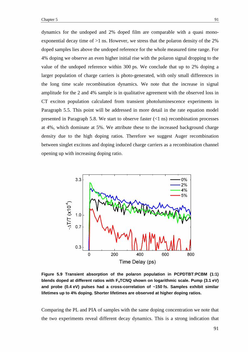
Chapter 5 91
91
dynamics for the undoped and 2% doped film are comparable with a quasi mono-
exponential decay time of >1 ns. However, we stress that the polaron density of the 2%
doped samples lies above the undoped reference for the whole measured time range. For
4% doping we observe an even higher initial rise with the polaron signal dropping to the
value of the undoped reference within 300 ps. We conclude that up to 2% doping a
larger population of charge carriers is photo-generated, with only small differences in
the long time scale recombination dynamics. We note that the increase in signal
amplitude for the 2 and 4% sample is in qualitative agreement with the observed loss in
CT exciton population calculated from transient photoluminescence experiments in
Paragraph 5.5. This point will be addressed in more detail in the rate equation model
presented in Paragraph 5.8. We start to observe faster (<1 ns) recombination processes
at 4%, which dominate at 5%. We attribute these to the increased background charge
density due to the high doping ratios. Therefore we suggest Auger recombination
between singlet excitons and doping induced charge carriers as a recombination channel
opening up with increasing doping ratio.
Figure 5.9 Transient absorption of the polaron population in PCPDTBT:PCBM (1:1)
blends doped at different ratios with F4TCNQ shown on logarithmic scale. Pump (3.1 eV)
and probe (0.4 eV) pulses had a cross-correlation of ~150 fs. Samples exhibit similar
lifetimes up to 4% doping. Shorter lifetimes are observed at higher doping ratios.
Comparing the PL and PIA of samples with the same doping concentration we note that
the two experiments reveal different decay dynamics. This is a strong indication that

92
92
recombination of charges populating the CT state and of separated polaron states
follows two distinct mechanisms apparently not interrelated. The experiments described
in Figure 5.7 and Figure 5.8 suggest that the introduction of a higher hole density by
doping is influencing the fate of photo-excitations at early times during the formation of
emissive CT excitons. Consistent with this picture is the decrease in the PL and the
larger PIA T/T from polarons at time zero. The observations exclude that the CT
emission intensity is quenched because of a non-radiative recombination channel, at
least up to 4% doping, and point to the fact that doping influences whether the initial
photo-excitations will form an emissive CT exciton or will result quasi-instantaneously
in separated polarons. To address this interpretation, a rate equation model is set up in
Paragraph 5.8 to fit the experimental results and study the rate constants for CT exciton
and polaron formation.
5.7 Effect of doping on the polaron signal in transient
absorption of PCPDTBT films
In order to assign the observed increase in polaron yield upon doping to effects
occurring at the interface between polymer and fullerene, doping induced changes on
the charge generation in the pure polymer have to be excluded. Therefore the transient
absorption of polarons in pure PCPDTBT films doped at different ratios with F4TCNQ
is investigated (Figure 5.10). We assume that in blends the dopants are equally
distributed in both phases. Thus, the dopant concentration in pure PCPDTBT films
corresponds to twice the values of blends. The results for the polaron yield in undoped
polymer films (black line) show a fast initial rise of the polaron signal within the
resolution of the setup and a faster decay (τ=3.7 ps) compared to the blend films. This
faster recombination is a typical result for polaron signals in pure organic polymer films
without an acceptor phase for efficient long-range charge separation. The polaron signal
for 1% doped polymer films (red line) shows an identical rise and decay without
differences in amplitude or lifetime compared to the undoped polymer. At higher
doping ratios (2%) the signal amplitude is slightly reduced, which we attribute to Auger
recombination effects, as mentioned in Paragraph 5.6.

Chapter 5 93
93
Figure 5.10 Transient absorption of the polaron population in PCPDTBT films doped at
different ratios with F4TCNQ. Pump (3.1 eV) and probe (0.4 eV) pulses had a cross-
correlation of ~150 fs. No significant changes in amplitude and lifetime are observed up
to 2% doping.
An increase in polaron signal as observed for doped blend films is not visible for pure
PCPDTBT. This result indicates that the observed increase in polaron density for doped
blend films is not due to processes related to the pure polymer phase, since in doped
polymer films one observes no change or, for higher doping ratios, even a decrease in
polaron signal.
5.8 Reduced CT exciton formation rate indicated by fitting of
experimental results with rate equation model
To discuss our observations in a more quantitative way, we modelled the PL and PIA
transients with a system of coupled rate equations. The model, based on the scheme of
Figure 5.11, considers that the initially photo-generated Frenkel excitons can form CT
excitons or polarons with two different probabilities given by the time constants CT-f
and P-f. Frenkel and CT excitons can recombine giving rise to the first (τFR-r) and
second (τCT-r) component of the PL decay in Figure 5.7, while polarons are detected in
the PIA experiment. The set of rate equations used for the simulations is given in
Equations (5-2) to (5-4). In these equations [FR], [CT] and [P] represent the population
densities for Frenkel excitons, radiative CT excitons and polarons, respectively. The

94
94
different time constants are τFR-r, τCT-f, τP-f, τCT-r and τP-r which correspond to the
recombination time of Frenkel excitons in PCPDTBT, the transfer time to a CT exciton,
the charge transfer time to separated polarons, the recombination time of the CT exciton
and the recombination time of the polarons.
Figure 5.11 Energy scheme for the HOMO and LUMO levels of PCPDTBT and PCBM
together with the transitions used in the rate equation model.
The model is intentionally kept as simple as possible, neglecting further details of the
charge separation process, since the focus of the simulation is on the role of CT excitons
in charge separation.
[ ]( )
[ ]( )
[ ]( )
[ ]( )
(5-2)
[ ]( )
[ ]( )
[ ]( )
(5-3)
[ ]( )
[ ]( )
[ ]( )
(5-4)
We note that a model considering the generation of polarons from dissociation of CT
excitons was not capable of fitting our experimental results. Since undoped
PCPDTBT:PCBM blends exhibit a photo-induced electron transfer on a time scale of
200 fs 78
, we have considered this value for P-f and CT-f in the undoped sample. The
recombination time of CT excitons (CT-r) was fixed at 300 ps for all the samples up to
4% doping, as well as the recombination time of Frenkel excitons in PCPDTBT at
125 ps. The values for these parameters were determined from transient

Chapter 5 95
95
photoluminescence experiments. For 5% doped samples the recombination times were
varied to obtain the best fitting to the experimental data.
The simulated transients, reported as symbols in Figure 5.7 and Figure 5.8, are in good
agreement with the experiments. Differences in the signal amplitudes of transient PL
and transient PIA, which are the most important observations of our study, are
quantitatively described by variations in the initial formation rate of recombining CT
excitons. This rate (expressed as inverse lifetimes) is as high as 1/0.2 ps for undoped
samples, but reduces to1/0.5 ps at 2% doping and 1/0.95 ps at 4-5% (Table 5.1). In our
model, CT exciton formation and polaron formation are competing processes. By
reducing the formation rate of recombining CT excitons while keeping the formation
rate for polarons constant, the probability of polaron formation is becoming more
probable. The reduced formation rate of recombining CT excitons is our main finding
and demonstrates the underlying mechanism behind the increased polaron yield,
observed in doped samples.
Doping [%] τFR-r [ps] τCT-f [ps] τP-f [ps] τCT-r [ps] τP-r [ps]
0 125 0.2 0.2 300 1400
2 125 0.5 0.2 300 1000
4 125 0.95 0.2 300 400
5 0.15 0.95 0.2 250 300
Table 5.1 Parameters used in rate equation model to fit the experimental PL and PIA data
for doped PCPDTBT:PCBM blends
he PIA decays for the 4 and 5% sample were modelled with shorter recombination
lifetimes of Frenkel excitons and polarons. This confirms that additional recombination
processes such as exciton-polaron quenching, i.e. Auger processes, are occurring. Based
on the mechanism proposed in this model we state that Frenkel excitons in the presence
of doped polymer chains are less prone to form recombining CT excitons. This leads to
a more favourable formation of polarons up to 4% doping. For the 5% sample faster
Frenkel exciton and polaron recombination channels are activated on a time scale of
150 fs and 300 ps, respectively.

96
96
5.9 Doping induced efficiency enhancement in solar cell
performance
The investigated blends have attracted substantial interest as active layers in
photovoltaic applications recently 120,121,131
. In order to study the effect of doping on the
photovoltaic performance, solar cells with doped PCPDTBT:PCBM layers were
fabricated. It has been shown recently that the addition of additives like 1,8-
diiodooctane can improve the solar cell performance 130
. We chose not to use additives
in order to keep the active layer properties similar to the spectroscopic samples.
However, to obtain significant solar cell performance, the PCPDTBT:PCBM ratio had
to be increased to 1:2. We assign this to the formation of improved charge percolation
pathways at higher PCBM content. Figure 5.12 shows the current density–voltage (I-V)
curves for PCPDTBT:PCBM blends with F4TCNQ doped at different ratios.
Figure 5.12 I-V curves for PCPDTBT:PCBM blends (1:2) doped with F4TCNQ at different
ratios, recorded with an AM1.5 solar simulator. An increase in short-circuit current is
observed for 0.5% doping. No significant changes in open circuit voltage or fill factor are
measured. For higher doping ratios the short circuit current and solar cell performance
decrease.
We find an increase in short circuit current JSC from 9.66 mA/cm² in the undoped cells
to 10.31 mA/cm² for 0.5% doping. Also the open circuit voltage VOC rises from 0.59 V
to 0.62 V. No significant changes in fill factor (FF) are observed up to 0.5% doping.

Chapter 5 97
97
Accordingly, the higher JSC and VOC lead to an improvement in power conversion
efficiency from 3.3% to 3.6%. These observations are consistent with the increased
polaron yield upon doping, as seen from spectroscopic measurements in Paragraph 5.6.
For higher doping ratios (1%), the cell performance falls below the undoped reference.
This effect is mainly due to a lower JSC and FF. We assign the reduced performance at
higher doping ratios to exciton-polaron recombination processes due to the dopant
induced background charge density. Interestingly, the doping ratios used in cells had to
be lower than in the spectroscopic studies, which can be rationalized by the charge
carrier extraction in solar cells. During transport to the electrodes on a microsecond
scale a larger volume is sampled, which makes interactions with doping induced
localized charge carriers more likely. Therefore recombination losses through these trap
states are more pronounced in cell performance than in optical spectroscopy, which was
only probing the first nanosecond after charge generation.
Another aspect of doping with respect to solar cell performance lies in the effects on
electrical properties. IV curves for doped and undoped solar cells measured without
illumination are shown in Figure 5.13.
Figure 5.13 I-V curves for PCPDTBT:PCBM blends (1:2) doped at different ratios with
F4TCNQ recorded in the dark. An increase in hole conductivity with increasing doping is
observed up to 1% doping.

98
98
One observes an increase in current density upon doping for holes and also electrons. A
positive effect of doping on conductivity has been shown for pure polymers before 11
and, as our results indicate, can also be observed in polymer:fullerene blends.
Therefore, the increase in cell performance is also partially due to improvements in
charge carrier extraction and transport. For further information on the effects of doping
on electrical properties in polymer:fullerene blends the reader is referred to a detailed
study published recently together with our collaborators 172
.
5.10 Assignment of reduced CT exciton recombination loss in
doped films to phase space filling
Considering the density of states (DOS) of conjugated polymers, which is broadened by
disorder in amorphous films, doping is known to fill the states at low energy in the tail
of the DOS 10
. To confirm that the charge carriers fill the states of PCPDTBT, we
looked at the high energy side of the PL spectrum, since the lowest energy part of the
DOS will be blocked for holes constituting Frenkel excitons. By this, the energy gap
will be shifted to higher energies and any emission should be blue-shifted. Because of
the undetectable PL from PCPDTBT in blends we show in Figure 5.14 the spectra of
pure PCPDTBT films doped by different amounts of F4TCNQ.
The PL peak position, representing the recombination of Frenkel excitons, is shifted
toward higher energies by 24 meV and 40 meV for the 2 and 5% doped sample,
respectively. This indicates phase space-filling of low-energy, immobile states in the
polymer HOMO and consequently blocking of these states (Figure 5.14, inset). We
interpret these states in PCPDTBT to be likely responsible for being sites where CT
excitons are formed and recombine. A possible interpretation of our observations is that
doped polymer domains do not support the formation of CT excitons resulting in a more
favourable formation of polarons. The increased separation of polarons might be further
attributed to a higher average mobility of holes in the polymer HOMO, since the low-
energy, immobile states are blocked by doping. Accordingly, photo-generated holes will
occupy energy levels with a higher DOS, providing more available states for hopping
transport. Because of the disordered nature of conjugated polymers, doping acts in an
inhomogeneous way leaving some domains unaffected. Those are likely to exhibit the
observed residual CT exciton emission.
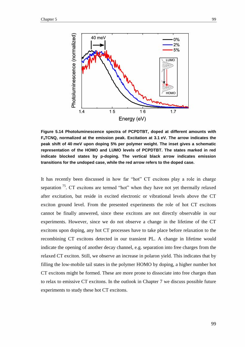
Chapter 5 99
99
Figure 5.14 Photoluminescence spectra of PCPDTBT, doped at different amounts with
F4TCNQ, normalized at the emission peak. Excitation at 3.1 eV. The arrow indicates the
peak shift of 40 meV upon doping 5% per polymer weight. The inset gives a schematic
representation of the HOMO and LUMO levels of PCPDTBT. The states marked in red
indicate blocked states by p-doping. The vertical black arrow indicates emission
transitions for the undoped case, while the red arrow refers to the doped case.
It has recently been discussed in how far “hot” CT excitons play a role in charge
separation 75
. CT excitons are termed “hot” when they have not yet thermally relaxed
after excitation, but reside in excited electronic or vibrational levels above the CT
exciton ground level. From the presented experiments the role of hot CT excitons
cannot be finally answered, since these excitons are not directly observable in our
experiments. However, since we do not observe a change in the lifetime of the CT
excitons upon doping, any hot CT processes have to take place before relaxation to the
recombining CT excitons detected in our transient PL. A change in lifetime would
indicate the opening of another decay channel, e.g. separation into free charges from the
relaxed CT exciton. Still, we observe an increase in polaron yield. This indicates that by
filling the low-mobile tail states in the polymer HOMO by doping, a higher number hot
CT excitons might be formed. These are more prone to dissociate into free charges than
to relax to emissive CT excitons. In the outlook in Chapter 7 we discuss possible future
experiments to study these hot CT excitons.

100
100
5.11 Conclusion
We enhanced the charge carrier generation in PCPDTBT:PCBM blends by using
chemical doping to change the electronic properties of the system. We employed
transient PL to investigate the effect of doping on the radiative recombination of
electron-hole pairs localized at conjugated polymer–fullerene interfaces (CT excitons).
Additionally, we used transient PIA measurements to probe the polaron formation and
recombination. We demonstrated that a low concentration of p-type dopant molecules
(< 4% weight) reduces the interfacial recombination via CT excitons and results in a
favoured formation of separated charge carriers. This was observed by an ultrafast
quenching of the CT exciton PL and an increase in photo-induced polaron density by up
to 70%. Results for doped prototype solar cells demonstrated an increase in open-circuit
current, in line with the spectroscopically observed higher polaron yield. The results are
consistent with a reduced formation of emissive CT excitons, induced by state filling of
the low-energy, immobile tail states in the polymer HOMO density of states. This work
shows that doping-induced state-filling influences the charge separation process and
offers a new interesting method to improve charge generation in organic photovoltaics.

101
101
6 Effect of oxygen doping induced degradation on
exciton dynamics and charge separation in
P3HT:PCBM blends
In this chapter, we describe the influence of oxygen doping induced degradation on the
fundamental photo-physical processes in P3HT:PCBM blends. Samples are
systematically aged by exposure to AM 1.5 illumination in the presence of dry air. The
amount of degradation is quantified by the relative absorption loss of P3HT and is used
to label the different investigated samples in the range from 0 to 20% degradation.
Steady-state PL spectra show an increasing loss in the number of excitons within P3HT
domains as a function of degradation. This loss already occurs within the first 15 ps
after photo-excitation, as revealed by transient photo-induced absorption (PIA)
spectroscopy of the exciton population. With the same technique we detect a more
pronounced, degradation-induced, decrease in polaron population compared to
excitons. This polaron loss occurs on a picoseconds time scale. Notably, the steady-
state PIA of degraded samples exhibits a signal ascribed to triplet excitons, which is
absent for undegraded samples. We attribute this to an oxygen doping induced
disruption of the pristine blend morphology. The investigation of polaron and exciton
population dynamics on a timescale from femtoseconds to one nanosecond, unravel two
primary loss mechanisms on the performance of degraded P3HT:PCBM solar cells:
The first process is an initial ultrafast decrease in the polaron generation, unrelated to
exciton diffusion to the polymer:fullerene interface. The second, less pronounced, effect
is a loss in the exciton population within the photo-excited P3HT domains. By
quantifying the loss mechanisms with a coupled rate equation model, we provide a
complete overview of the degradation effects on the photo-physics in P3HT:PCBM
blends. In addition, we report solar cells fabricated from degraded blends and compare
our spectroscopic findings with power conversion efficiency measurements.

102
102
6.1 Motivation to study oxygen doping induced degradation
processes
Organic solar cells continue to attract large interest because of their potential for simple
processing, light weight applications and low production costs 25
. During recent years
the power conversion efficiencies of both, single-junction and tandem-cell devices, have
improved significantly 127,212
. Recent reports show photovoltaic efficiencies above 8%
from a combination of low bandgap donor-acceptor copolymers and a fullerene
derivative 122,127,213
. A topic, which is just as important for commercialization, but has
not been investigated in detail, is the long-term device stability. One major issue
concerns the diffusion of oxygen into the active layer under ambient conditions214–217
.
The concomitant reactions of oxygen with the organic semiconductor218,219
leads to a
loss in device performance220–222
and is termed degradation. Indeed, estimations on the
costs of production and cells lifetime indicate that organic photovoltaics can become
competitive with other technologies, if module lifetimes between 5 and 10 years are
reached 25,223
. So far, studies on the long term stability and the degradation of solar cells
have been mainly focussed on the complete devices221,222,224–227
. While those are of
primary importance, it is not always possible to distinguish between the degradation of
the active layer, the interface with the electrodes, or the contacts 228,229
. In devices with
regular structure the corrosion of the low workfunction electrodes usually limits the
lifetime 227
, while for cells of inverted structure the degradation under illumination in
dry air affects mainly the active layer. The degradation effects consist of a reversible
part, which is assigned to oxygen induced chemical doping, and an irreversible part
which is due to p-doping and photo-oxidation of the polymer 230
. In our work we
investigate the irreversible effects of degradation on the photovoltaic processes in the
active layer, each of which might be adversely influenced.
There are several physical processes contributing to photocurrent generation in a typical
polymer:fullerene solar cell. First, bound electron-hole pairs are created upon light
absorption. This process primarily takes place in the conjugated polymer, due to the
high absorption cross-section of optical transitions in these materials. On the other hand,
in common fullerene derivatives these transitions are typically forbidden and, thus,
weak153,157,231
. The electron-hole pairs form excitons that diffuse through the material,
with the vast majority reaching the heterojunction, before recombining 80,208
. Electron
transfer takes place, provided that an optimal bulk heterojunction morphology is
Chapter 6 103
103
present 22,232,233
. This either leads to the separation of charge carriers or to the formation
of interfacial CT excitons, which can recombine radiatively 90,101,103,111
. Separated
positive and negative charge carriers (polarons) then move towards the electrodes
within the polymer and fullerene domains, respectively. The photocurrent is the result
of polaron drift and extraction at the electrodes. So far, the contribution of each of these
processes in limiting the performance of degraded devices has not been clarified yet. In
other words, it is not clear whether excitons, polarons or the CT excitons are mainly
affected by degradation and to which extent. The degradation of the polymer:fullerene
active layer, occurring upon extended illumination in atmosphere, can in principle
impact each of the physical processes described above. For example, exciton
recombination via dark states could be accelerated. This would negatively influence the
total amount of polaron pairs, which are supposed to be generated at the heterojunction.
Moreover, polarons might be trapped at degradation sites and their recombination rate
could increase. This effect is explained by the loss in the average carrier mobility,
which is known to accelerate recombination 144,234
.
6.2 Controlled oxygen doping of polymer-fullerene blends
P3HT with a regio-regularity higher than 90% was provided by Merck. PCBM(60) was
purchased from Solenne and used as received. For all the blends (1:0.8 weight ratio),
solutions of the polymer and fullerene were prepared in spectroscopic grade o-xylene.
Thin films of the blends were obtained by doctor-blading on pre-cleaned glass
substrates in inert atmosphere. Prior to degradation, the films were annealed at 140 °C
in the glovebox for 2 min. Subsequently, the samples were exposed to oxygen in dry
synthetic air and illuminated with the full spectrum of a sun simulator (AM1.5 solar
spectrum) until the desired amount of degradation was achieved. The duration, until the
final degradation level was reached, was in the order of a few hours. Before performing
spectroscopy on the degraded samples, they were brought back into the glove box and
encapsulated. For this a glass plate was put on top of the film and the edges were sealed
with gas-tight epoxy resin (Torrseal®). In order to remove any reversibly bound oxygen
from the films, the samples were annealed in the glovebox at 130 °C for 10 min prior to
encapsulation. The encapsulation under inert conditions prevents any further exposure
to oxygen that might lead to changes in the samples’ properties. This allowed us to use
the same set of samples for all the presented experiments.

104
104
Figure 6.1 shows the absorption spectra of four P3HT:PCBM blends with different
exposure time to oxygen (dry air) and AM1.5 solar simulator illumination at room
temperature. All spectra show the typical absorption features of annealed P3HT:PCBM
blends in the visible and ultraviolet (UV) 138
. The absorption band from 400 nm to
700 nm is due to P3HT. In particular, the absorption shoulder around 600 nm represents
the crystalline phase of P3HT, indicating the presence of highly ordered P3HT domains
in the blend. PCBM shows a strong absorption in the UV below 350 nm and has only a
weak absorption tail extending into the visible 153
. While the P3HT absorption band is
monotonically decreasing with exposure time, the absorption of PCBM, which is more
pronounced in the UV below 350 nm, is less affected.
Figure 6.1 Absorption spectra of P3HT:PCBM blends subjected to different ageing
periods under oxygen (dry synthetic air) and AM1.5 solar illumination. The spectra show
a homogeneous loss in the absorption range of P3HT (400 nm – 650 nm) while the PCBM
absorption is less affected (<400 nm). The relative loss in absorption (in %) at 500 nm is
used to label the degradation of the samples, as stated in the legend.
This observation suggests that PCBM is less severely influenced by degradation and
less prone to suffer from oxygen doping, compared to P3HT. Remarkably, the decrease
in the absorption spectrum of P3HT is wavelength independent, i.e. all spectra have
similar shapes, and only a very weak feature on the red onset of the absorption is
noticed after relative subtraction of the spectra. This feature can be considered as an
indication for the formation of a charge transfer complex between P3HT and oxygen 219

Chapter 6 105
105
or some degradation product 235
. According to the results of Reese et al. 236
, the short
ageing periods used in our study exclude changes to the initial morphology after
preparation of the blends. The relative loss of the absorption (in %) at 500 nm is used in
the following to classify the samples, where 0% corresponds to the undegraded sample.
6.3 Observation of degradation-induced exciton population
loss in steady state photoluminescence
We use photoluminescence (PL) spectroscopy as a suitable tool to study the effect of
degradation on the photo-generated singlet Frenkel excitons in the polymer-fullerene
blend. Figure 6.2 shows the PL spectra of blends at the same degradation stages as
shown in the previous paragraph. The spectrum is dominated by the characteristic P3HT
emission 137
and the PL intensity decreases monotonically with degradation. The inset in
Figure 6.2 shows normalized PL spectra.
Figure 6.2 Photoluminescence spectra of P3HT:PCBM blends at different degradation
stages. Excitation wavelength was 500 nm. The inset shows the normalized
photoluminescence spectra. A monotonous quenching of the emission with increasing
degradation is observed. The shape of the spectra changes only slightly in the region of
the crystalline P3HT domains, as shown in the inset.
Interestingly, the shoulder around 650 nm which is representative for crystalline
domains in P3HT is more strongly quenched than other regions of the spectrum. This

106
106
might indicate a break-up of the crystallinity, resulting from oxygen diffusion into these
domains. On the other hand the presence of oxygen is known to quench PL. Therefore,
a further explanation of the PL quenching might be a stronger accumulation of oxygen
molecules in the crystalline, compared to the amorphous domains, leading to a stronger
PL quenching in the crystalline domains. However, this is only a minor effect. Further
insights on the PL quenching mechanism can be gained from the quantitative loss in
emission intensity. In Figure 6.3 we report the ratio between the integrated P3HT PL of
the undegraded blend, PL(0%), and the degraded samples, PL(x%), where x indicates
the relative level of ageing according to Figure 6.1. The values are plotted versus the
relative change in absorption which is a measure for the oxygen doping of the
sample 237
. The integrated PL is evaluated after rescaling for the amount of photons
absorbed at the excitation wavelength of 500 nm.
Figure 6.3 Ratio between the integrated PL of the undegraded sample [PL(0%)] and
degraded samples [PL(x%)], plotted against the degradation ratio as determined from
absorption measurements. The drawn line represents a linear fit to the data. The linear
relation indicates a Stern-Volmer type of quenching.
We evaluate the data on the basis of a Stern-Vollmer relationship. The data indicate a
linear relation, typical of a Stern-Volmer type of quenching 65
. The Stern-Vollmer
relationship describes the quenching of an excited molecule in the presence of a
quencher species according to the formula:

Chapter 6 107
107
[ ] (6-1)
In this equation I0 stands for the PL intensity without quenchers, while I describe the
intensity in the presence of quenchers with concentration [Q]. k is the Stern-Vollmer
constant.
The Stern-Volmer behaviour indicates that excitons, diffusing in polymer domains,
encounter quenching sites, whose number increases linearly with the amount of oxygen
doping. It has been found in previous publications that the amount of degradation
increases with exposure time to oxygen and illumination 214,237,238
. This suggests that
blend films exposed to illumination in air for longer time intervals have a higher
concentration of quenching sites, generated by the photo-oxidation process. We assign
those sites to be dark, since we were unable to detect significant differences in the shape
of the PL spectra in the visible and near infrared up to 1400 nm. Summarizing the
information extracted from PL experiments, photo-generated excitons in P3HT can
decay non-radiatively as a consequence of interaction with dark species produced in the
degradation process. Some excitons might also be quenched by charge carriers, which
are either a result of the ground state CT complex 219
formed with O2 or originating
from degradation radical reactions 239
as shown in previous publications. For excitons in
P3HT these processes represent loss channels competing with diffusion to the
heterojunction interface and charge separation.
6.4 Reduced initial polaron and exciton populations with
faster recombination dynamics
The PL data of Figure 6.2 provide valuable information on the quenching of P3HT
excitons by degradation, but do not offer a probe for the charge generation. This process
takes place at the interface (heterojunction) with PCBM and gives rise to the formation
of polarons, responsible for the photocurrent. An experimental technique, which gives
unique insights into the population dynamics of excitons and polarons, is photo-induced
absorption (PIA) spectroscopy. We first comment on the different signals obtained in
PIA experiments in steady-state conditions and then focus on the dynamics on a
picosecond time scale.

108
108
Figure 6.4 shows the steady-state PIA of samples at different degradation stages. In PIA
experiments the relative change in transmission T/T through the blend film, induced
by photo-excited states, is measured. The states are induced by a cw-laser tuned to
532 nm. Positive signals (note the –T/T in our scale) indicate an increase in the
transmitted probe light and can originate from ground state bleaching (GSB) or
stimulated emission (SE). Negative signals are due to a decrease in the transmitted light
and originate from absorption of excitons towards higher excited states or from
absorption of polarons.
Figure 6.4 Steady-state PIA of P3HT:PCBM blends at 0 and 10% degradation measured
with excitation at 532 nm. Spectra normalized to the ground state bleach (GSB) at 600 nm
to obtain comparable excitation densities. Note the break in the ΔT/T axis. Undegraded
blends show GSB below 650 nm and polaron signals between 650 nm and 1050 nm. In
degraded samples the polaron signal intensities are reduced and a new band at 850 nm
rises, which was assigned to triplets previously. Image adapted from Deschler et al. 240
,
measurement by Dr. A. De Sio at Carl von Ossietzky Universität, Oldenburg.
The steady-state PIA spectrum of P3HT:PCBM is dominated by the optical transition of
species in P3HT, which have been previously studied and interpreted 211
. The band at
670 nm has been assigned to a signature of delocalized polarons (DP), meaning
polarons delocalized over two or more polymeric chains, while the weak signal above
1100 nm is due to transitions from the first excitonic state (S1) to higher exciton states
(Sn) 26,211
. We term these last transitions “exciton absorption” (ExA). The ExA
absorption is expected to be weak in a steady-state experiment, because of the short

Chapter 6 109
109
lived nature of excitons in a polymer fullerene blend. This signal represents a measure
for the exciton population in the blends. Previous publications have shown that ExA
transitions extend up to 1600nm 159
. Peaks at 850 nm are due to triplet exciton
absorption (T1→Tn) and features around 1000 nm originate from localized polarons
(LP) with intrachain character 241
.
We note that there is a decrease in the amplitude of the DP signal upon ageing,
indicating that degradation has an influence on the population of polarons, which are
fundamental for photovoltaic action. While the 0% sample (black curve) has only two
prominent bands at 670 nm (DP) and ~1000 nm (LP), both due to polarons, the 10%
sample exhibits a signal at 850 nm, which we assign to triplet exciton absorption (TrA).
This excited state transition is usually not observed in regioregular P3HT in blends with
PCBM, since the relatively high yield of polaron formation in the excited state
competes with intersystem crossing and population of the triplet state 208
. However, PIA
measurements on regio-random P3HT, where polymer chains are more disordered and
polaron generation is less probable 103,159
, indicate the presence of a band at 850 nm
with spin-1 characteristics, i.e. a triplet 211,242
. The formation of a triplet band in
degraded blends therefore indicates more disordered films with an increased number of
sites where intersystem crossing can occur. We attribute this to oxygen diffusion into
the blend films and concomitant breaking of the pristine blend morphology. We note
little changes in the ExA spectral range among the different samples. However, due to
the short lived nature of singlet excitons in P3HT:PCBM those are almost undetectable
in steady-state experiments as the one shown in Figure 6.4. We address this point in a
more quantitative manner below, by analysing the ExA signal in transient absorption.
Furthermore, the measurements of ExA transitions on a picosecond time scale, within
the lifetime of the excitons, allow for a detection of the short-lived exciton states.
In order to probe the exciton population dynamics (ExA), we performed femtosecond
transient absorption spectroscopy by exciting the sample with 200 fs short pulses
centred at 550 nm and recording the change in transmission of time delayed pulses at
1500 nm. This probe wavelength allows us to observe the decay of ExA, in a spectral
region without the interfering contribution of P3HT polarons 159
. However, we have
removed a small, long-living constant background, likely caused by a weak polaron
signal from PCBM, since its anion is expected to absorb in this region243
. All
measurements were corrected for differences in absorption at the excitation wavelength
of 550 nm.

110
110
Figure 6.5a shows the T/T transients probing the ExA at 1500 nm for blends of
different degradation level (0%, 10%, 20%). For all samples the signal sets in within the
setup’s time resolution of ~250 fs, but shows different amplitudes at zero time delay for
degraded samples (10%, green curve / 20%, blue curve) compared to the undegraded
blend (0%, red curve). This indicates that in degraded samples part of the initial hot
excitons are lost within the first 250 fs. Looking at the ExA decay in the first
picoseconds after exciton thermalization (Figure 6.5a), we note that degradation leads to
faster recombination and shorter lifetimes. In the first picoseconds after excitation
typically the exciton diffusion process is observed. Faster dynamics on this time scale
suggest that exciton quenching during the diffusion process contributes to the loss in the
overall exciton population as well.
Figure 6.5 Transient absorption decays for P3HT:PCBM blends with the probe centred in
the absorption bands of excited singlet state (ExA, 1500 nm) and delocalized polaron
(DP, 700 nm), respectively. In (a,b) transient rise and decays are shown on a short time
scale (0-15 ps). In (c,d) transient decays are shown on a long time scale (0-900 ps) for
ExA and DP, respectively. Symbols in (c,d) are data points whereas the solid lines
represent fits according to the rate equation model described in the text. Excitation
performed at 550 nm with fluences <10µJ/cm2. The transients have been rescaled for the
amount of photons absorbed, i.e. 1-10^(-OD) at the exciting wavelength.

Chapter 6 111
111
It is interesting to compare these decays with the dynamics of the delocalized polarons
(DP), which are supposed to be representative for the carriers contributing to
photocurrent in the solar cell 159
. In Figure 6.5b we report the transient dynamics of DPs
probed at 700 nm. The undegraded sample at zero time delay shows an ultrafast
negative feature (positive on a +T/T scale) slightly longer than the duration of the
pump pulses. It evolves into a positive signal with a rather long rise time, reaching a
maximum at about 40 ps. In the degraded samples (Figure 6.5b, green/blue curve) the
rise in DP is faster and the initial negative feature is absent. Further, the overall amount
of DP is smaller compared to the undegraded samples as the signals saturate at
0.52·10-2
, 0.35·10-2
and 0.29·10-2
for the 0, 10 and 20%, respectively. So far the rise of
the DP signal has been interpreted as the generation of free polarons from excitons
diffusing to the heterojunction or from charge transfer excitons 139,244
. However, as seen
from the transients of the undegraded blend in Figure 6.5(a,b), the rise in DP correlates
with the decay of excitons (ExA). In contrast to previous assignments we propose, that
the generation of DPs is not subjected to a rise, but that the T/T signal in this spectral
region is rather superimposed by a short lived stimulated emission (SE) feature 80
. The
SE dynamics resemble the ones of ExA (Figure 6.5a), since they originate from the
same species, i.e. excitons in the P3HT domains. Small differences in the dynamics are
observed, since SE originates only from excitons diffusing and recombining in the
P3HT domains. On the other hand, ExA considers all excitons photo-generated in
P3HT, i.e. those recombining, getting trapped or separating to form polarons at the
heterojunction. Further, the loss of excitons at time zero seen in the ExA transients
(Figure 6.5a) is reflected in the loss of the negative SE signal for the 10 and 20%
degraded samples in Figure 6.5b. For the 20% sample the rise of the DP signal is
instantaneous and therefore uncorrelated to a diffusion of excitons towards the interface
within several picoseconds. If the rise in DP were due to the splitting of excitons after
diffusion to the polymer:fullerene interface, the faster decay of ExA would mean a
faster, thus more efficient, generation of polarons. Such an effect is not observed, since
the DP amplitude decreases. In conclusion we assign the negative feature and rise
detected in the DP signal of undegraded blends to SE from diffusing excitons. This
interpretation is in agreement with recent experimental studies by infrared femtosecond
PIA spectroscopy, where polarons can be selectively probed in the absence of
superimposed stimulated emission contributions and appear without any rise on a

112
112
picoseconds time scale 80,95
. Further insights can be gained from the relative loss of
exciton (ExA) and polaron (DP) population in degraded samples. The relative loss is
obtained by comparing the maximum T/T, taken at zero time delay, for degraded and
undegraded samples. For the 10% degraded sample, we find a loss in exciton population
of 24% compared to the undegraded sample, while the polaron population is reduced by
33%. For the 20% sample, the initial loss in excitons is 31%, whereas the loss in DPs
amounts to 45%. The loss in DP compared to the loss in exciton population is therefore
more pronounced in all degraded samples. This indicates a more pronounced
degradation effect at the polymer:fullerene interface where charge generation occurs.
Further, a substantial amount of polarons is generated immediately after excitation and
not as a consequence of exciton diffusion to the interface.
To investigate the effect of oxygen doping on recombination dynamics on a longer time
scale, we investigated the transient absorption of ExA and DP up to 1 ns (Figure
6.5(c,d)). The ExA signal for pristine and degraded blends (Figure 6.5c) decays to zero
within the first 200 ps, indicating short-lived excitons. This correlates with the efficient
splitting of initially excited excitons into separated charges at the heterojunction. A
shorter exciton lifetime is observed for increasing degradation, as already indicated
from the experiments probing the first tens of picoseconds (Figure 6.5a). On the other
hand, the DP transient of the undegraded sample, (Figure 6.5d, red curve), does not
exhibit a decay on a time scale of 1 ns in accordance with previous studies on
undegraded P3HT:PCBM blends 80,159
. These studies show the long-lived nature of DPs,
which need to be extracted from the active layer and contribute to the photocurrent for
efficient solar cell performance. In contrast to the undegraded blend, the DP signal of
the 10 and 20% degraded samples exhibits an initial decay on the hundreds of
picoseconds time scale. This indicates that the products resulting from photo-oxidation
influence the polaron dynamics on a nanosecond time scale and evidently lead to
accelerated recombination. The reduced polaron lifetime in degraded samples hinders
charge extraction and is detrimental for efficient solar cell performance. In the next
paragraph the underlying processes will be quantified, employing a rate equation model.
Summarizing, degraded blends show reduced exciton as well polaron populations
compared to undegraded samples within the setup time resolution of 250 fs. We stress
that relative losses in exciton and polaron populations are not identical upon ageing of

Chapter 6 113
113
the blend. The loss in polarons is more severe with faster polaron recombination rates
for increasing degradation.
6.5 Quantification of loss processes with rate equation model
In order to obtain a quantitative estimation of the trapping rates induced by degradation
products, we have modelled the transient absorption curves with a system of coupled
rate equations. Figure 6.6 gives a schematic overview of the transitions described in the
rate equation model. First, we have considered the initial amount of hot excitons [HEx],
induced by the pump laser pulse. Excitons are termed “hot” when they have not yet
thermally relaxed after excitation, but reside in excited electronic or vibrational levels
above the exciton ground state. The [HEx] are branching into four different populations.
These are the recombining excitons [Exr], the diffusing excitons [Exd], free polarons
[Polf] and trapped excitons [Ext] according to the rate equation
[ ]
[ ]
[ ]
[ ]
[ ]
(6-2)
The initial ultrafast partition or branching of HEx is a necessary step to describe the
decrease in the signal of ExA and DP at zero time delay. This approach is consistent
with the experimental reports that excitons diffusing to the heterojunction are not the
exclusive source of polarons in P3HT:PCBM blends. It has been shown that polarons
can form quasi-instantaneously 80,95
from hot excitons. Equation (6-2) takes into
consideration that a portion of the initial [HEx] is generated in P3HT close enough to
the heterojunction interface to diffuse and reach PCBM, those constitute the diffusing
excitons, [Exd]. Some other [HEx] within the P3HT domains and far from the interface
are just recombining, [Exr], or are trapped to dark states because of degradation
products, [Ext]. The first term on the right hand side of eq. (6-2) takes into account the
direct formation of polarons from the [Hex] as evidenced from the experiments in
reference 80
. The time constants, or inverse probabilities, for the generation of free
polarons ( ), diffusing excitons ( ), recombining and trapped excitons
( ) and ( ), respectively, determine the initial branching ratios in Equation
(6-2).

114
114
Figure 6.6 Energy scheme for the HOMO and LUMO levels of P3HT and PCBM together
with the main transitions used in the rate equation model. The initial population of hot
excitons [Hex] is marked (1).
We have described the transient signal of ExA considering two contributions originating
from diffusing excitons
[ ]
[ ]
[ ]
[ ]
(6-3)
and recombining excitons
[ ]
[ ]
[ ]
(6-4)
Both populations are fed by [HEx], with the respective branching probabilities set by
and . The excitons in Equation (6-3) are influenced by diffusion to the
heterojunction, , or formation of trapped polarons, . On the other hand, the
excitons in Equation (6-4) recombine with the lifetime .
To model the transient DP absorption signal, we used two contributions originating
from free and trapped polarons, [Polf] and [Polt], which are described by
[ ]
[ ]
[ ]
[ ]
(6-5)
[ ]
[ ]
[ ]
(6-6)
Chapter 6 115
115
The lifetimes and describe the recombination time for free and trapped
polarons, respectively. The modelling with two polaron populations was necessary to
consider the bi-exponential decay of Figure 6.5d for the degraded samples.
From fitting the transient absorption of ExA and DP in the undegraded sample, we
obtained and in Equation (6-2). These rates are
consistent with the typical thermalization times of excitons in conjugated polymers 63
.
The values were then kept constant for the fitting of the degraded samples, since the rate
constants of these processes are not affected by degradation. Hence, degradation-
induced phenomena on [HEx] are described by variation of the rates of polaron
formation and trapping of hot excitons . In Equation (6-3) and (6-5)
we set and the rate of trapped polaron recombination .
These values are kept constant, since the dynamics of these processes are assumed not
to vary for different degradation extents. We took , as obtained from time
resolved PL experiments. The six transient absorption decay curves for ExA and DP at
0, 10 and 20% degradation were then fitted adjusting the remaining four decay times.
The simulated curves are shown as lines in Figure 6.5(c,d). The fittings accurately
describe the transient curves for all samples both in amplitude and dynamics. First, we
discuss the rates which were varied to reproduce the initial decrease in the amplitude of
ExA and DP signals at time zero (Table 6.1). We notice that , which is the
rate at which hot excitons turn into trapped excitons, is an important fitting parameter in
our model. At 0% this rate can be taken as small as (10 ps)-1
, since the other more
probable processes in Equation (6-2) dominate. However, for increasing degradation
levels it has to be set to substantially higher values up to (100 fs)-1
.
Degradation ratio
[fs] [ps] [fs] [ns]
0% 10·103 100 300 10
10% 200 30 500 8
20% 100 10 600 3
Table 6.1 Time constants for the different photophysical processes described in
Equations (6-2) to (6-6) of the rate equation model.
The initial decrease in DP signal is taken into account considering changes in
which has a lower probability (1/600 fs)-1
upon degradation, with respect to the 0%

116
116
sample (1/300 fs)-1
. For the different decays, the faster dynamics of ExA on a
picosecond time scale upon degradation are described by decreasing . This rate
is also used to generate the correct amount of trapped polarons to fit the DP curves. Our
model is capable of reproducing the long decay time of DP, which is dominated by two
lifetimes. Here, we have decreased the recombination time of free polarons, ,
from 10 ns in the 0% to 8 ns and 3 ns for the 10 and 20% samples, respectively, to fit
the long decay, while the first decay component is fixed at 175 ps. It describes the
recombination of trapped polarons. In summary, the coupled rate equation model allows
us to fit the experimental data and quantify the rates of the degradation-induced loss
processes.
From the spectroscopic results (Paragraph 6.4) and the coupled rate equation model
(Paragraph 6.5), we can assign the main degradation-induced loss processes. In Figure
6.7 we give an overview of the different trapping and recombination mechanisms
according to Table 6.1.
Figure 6.7 Energy schemes illustrating the main degradation processes occurring in
aged P3HT:PCBM blends. (a) Hot exciton trapping in P3HT (b) Exciton splitting by
degradation products to form trapped polarons in P3HT (c) Hindered charge transfer at
the interface between P3HT and PCBM (d) Increased recombination of free polarons in
P3HT. The processes illustrated here correspond to the lifetimes presented in Table 6.1.
We conclude that the ultrafast initial loss in ExA and DP is due to an increased
probability to trap hot excitons and a decreased probability to form free polarons
(Figure 6.7(a,c)). These two trends are summarized in the second and fourth columns of
Table 6.1 and determine the major initial losses. The faster decays observed in Figure
6.5a for the ExA upon degradation are assigned to the generation of trapped polarons by

Chapter 6 117
117
the diffusing excitons (Figure 6.7b). Finally, we attribute the faster decay in the DP
signal of degraded samples to an increased population of trapped polarons and faster
polaron recombination, which enters the nanosecond regime (Figure 6.7d). The initial
ultrafast processes account for the major initial loss in exciton and polaron population,
which are the critical species for the functioning of a solar cell. The long time scale of
DP recombination is significantly compromised for extensive degradation treatments, as
in the 20% sample. Here, the long lived polarons, which are contributing to the
photocurrent, show a bi-exponential decay with lifetimes of 8 and 3 ns. We suggest that
these shorter lifetimes are detrimental for efficient charge extraction. To examine this
prediction we have fabricated and measured solar cells from P3HT:PCBM blends
following the same ageing procedure as in the spectroscopic studies.
6.6 Effect of degradation on device performance
In order to quantify the effect of degradation on the device performance, the current-
voltage characteristics of P3HT:PCBM cells with inverted structure are measured for
different degradation ratios (Figure 6.8). Via absorption measurements the extent of
degradation was determined. To allow for measurements of absorption spectra on
complete device structures, the solar cell top electrode is designed as a grid finger
structure on top of a highly conductive PEDOT:PSS layer.This way, it is possible to
transmit light through the whole device and the absorption spectrum can be collected.
Figure 6.8 shows the current voltage characteristics of three photovoltaic cells, degraded
0, 2 and 5%. An absorption loss of the active layer by 5% results in the reduction of
device power conversion efficiency from 3.2% to about 0.3%. Longer ageing
periods, corresponding to a 10% degraded sample, resulted in the total absence of
photovoltaic response in the cells. This observed loss in cell performance is mainly due
to a decrease in the short circuit current, from 9.9 mA/cm2 to 1.6 mA/cm
2. The loss in
fill factor is less dramatic from FF = 0.59 to FF = 0.38. Interestingly, the open circuit
voltage is not affected by degradation up to 5%. The 85% loss in JSC for a device with
just 5% absorption loss is therefore a combination of several factors: about 24% are due
to the reduction of charge carrier formation (polarons) during the first 250 fs after the
laser pulse, as determined from transient absorption measurements on a 5% degraded
sample. We conclude that the remaining 61% of loss in extracted charge carriers are due
to the loss in absorption (5%) and enhanced charge carrier recombination on the µs time

118
118
scale, not accessible in the present experiments. An additional possible loss channel is
trapping in PCBM, which is not detectable in our experiments.
Figure 6.8 Current density vs. bias voltage measurements for P3HT:PCBM devices with
inverted cell geometry under illumination with a solar simulator before (red squares) and
after (yellow triangles and black circles) degradation under oxygen (dry synthetic air) and
AM1.5 illumination. The extent of degradation corresponds to an absorption loss of the
active layer by 2% (black circles) and 5% (yellow triangles). Image adapted from Deschler
et al. 240
, device fabricated and measured by T. Sauermann at Konarka Technologies.
6.7 Stronger effect of oxygen doping on polaron compared to
exciton populations
This paragraph discusses the results of the spectroscopic and solar cell performance
experiments on degraded blends. The analysis of our photo-physical data addresses the
processes responsible for the degradation of performance in P3HT:PCBM solar cells. In
particular, the data presented in Figure 6.5, together with the rate equation model in
Paragraph 6.5, identify a faster trapping of initial hot excitons and a less probable
formation of free polarons during exciton relaxation. Experimentally, the major losses
are observed within the setup temporal resolution of about 250 fs, while excitons have
not yet completely relaxed and are still “hot”. This indicates a higher probability for hot
excitons to be trapped by a degradation product. This observation can be rationalized,
considering that hot excitons are more delocalized and in a coherent state. In this
configuration they can sample a larger number of conjugated segments in the first few
hundred femtoseconds and are more prone to encounter degradation products 245
. The

Chapter 6 119
119
more significant loss in polarons, which results in the decrease of the maximum
amplitude of the DP absorption signal, is a combined consequence of hot exciton
trapping and a lower probability of free polaron formation. In undegraded systems,
separated polarons are formed on an ultrafast time scale (<100 fs), involving P3HT
chromophores close to the heterojunction interface. It is interesting that degradation of
the polymer domains, which is demonstrated by our absorption and PL experiments
(Figure 6.1 / Figure 6.2), is influencing the ultrafast charge generation process occurring
primarily for chromophores close to the interface. We suggest that the degradation
products, likely originating from photo-oxidation of the polymer, might be more
concentrated at the heterojunction. In this region the P3HT chains are at the border of a
semi-crystalline domain and oxygen can diffuse more easily into these areas compared
to the crystalline core parts. The shorter lifetimes of ExA observed upon degradation
have been modelled considering the formation of trapped polarons from diffusing
excitons. While we did not observe clear indications for the build-up of a triplet
population in the transient experiments, our steady state PIA indicates the presence of
this species on a longer time scale. To explain these observations, we recall that regio-
random P3HT shows signatures of triplets in PIA, while having the same chemical
structure of P3HT 211
. An important difference between the regio-regular P3HT used
here and the regio-random type is the conjugation length and the intrachain planarity,
two effects which are known to affect the triplet yield 246
. On the basis of these
arguments, we can discuss the increased triplet yield in degraded blends, considering
that degradation products might disrupt the conjugation of the polymer or create
carbonyl groups. As a result, intersystem crossing to the triplet manifold is enhanced 66
.
The comparison between the losses in DP population and the JSC of solar cells
underlines that a large part of the photovoltaic performance drop is ascribed to an
increase in the long time scale recombination of polarons (>10 ns). This might also
involve charge trapping in PCBM. In this direction, the recent work by Reese et al.
reports the presence of PCBM degradation products acting as effective traps for the
transferred electrons 182
.
6.8 Conclusion
We performed a photo-physical study on the fundamental processes concerning
photovoltaic operation in P3HT:PCBM blends subjected to different extents of oxygen

120
120
doping. Illumination of oxygen doped samples leads to photo-oxidation, also termed
degradation. The blend films were labelled according to the relative degradation-
induced absorption losses. PL spectroscopy indicated a linearly increasing density of
exciton quenching sites with degradation. Evaluation of exciton and polaron populations
from transient PIA measurements allowed quantification of the degradation-induced
losses. The fitting of the experimental results with a rate equation model allowed
quantification of the individual loss channels. Our analysis indicated that exciton
trapping takes place on a rate comparable to electron transfer to PCBM. Additionally,
ageing has major consequences on the polaron population. The polaron generation is
reduced with degradation and has to compete with the fast hot exciton trapping
processes. Further, degradation reduces the lifetime of separated charge carriers which
inhibits charge extraction from the active layer. Additionally our results suggested that
the crystalline phase of P3HT domains is disrupted by migrating oxygen molecules.
This leads to less efficient polaron formation and an increased triplet yield.
Accordingly, prototype solar cells show a critical performance loss upon degradation.
The experimental results assigned the lower cell efficiency to absorption losses, exciton
trapping and reduced polaron formation. Our results have important implications on the
understanding of degradation related phenomena in organic solar cells and on the
modelling of device losses in aged photovoltaic devices.

121
121
7 Summary and Outlook
This thesis investigated the effects of small molecule doping on the charge separation
process in conjugated polymer:fullerene heterojunctions. Depending on the type of
dopant employed, improved or reduced charge generation was observed. The interaction
of the dopant with the host material and the resulting changes in electronic and chemical
properties determined the eventual result. The insights gained from these results offer
new promising directions to improve solar cell performance.
In the first part of this thesis, we investigated the distribution of dopant molecules
(F4TCNQ) in conjugated polymers. We demonstrated, to our knowledge for the first
time, that dopant distributions in thin polymer films can be mapped with low-voltage
SEM. For different polymers, significant differences are observed in the doped film
morphology. Aggregation and clustering of dopant molecules occurs above defined
threshold doping ratios. We assign the differences in threshold values to differences in
interaction between dopant and conjugated polymer.
With the presented general technique, the dopant distribution in various dopant-polymer
systems can be studied. These future experiments will give further insights on dopant-
polymer interaction and dopant-induced changes in polymer morphology. Further, SEM
mapping of dopants might also be possible for the more ordered, small molecule
organic semiconductors. Additionally, the increase in SEM contrast for organic
semiconductor films, containing electron accepting dopants (p-doping), should also be
observable using electron donating dopants (n-doping). Therefore, another interesting
future experiment is the mapping of n-type dopants,e.g. cobaltocene.
Further, we have shown that p-doping of a low-bandgap polymer:fullerene blend with a
small molecule electron acceptor (F4TCNQ) results in reduced recombination through
CT excitons. This effect causes an concomitantly improved photo-induced charge
generation. We explain the observed effects by phase-space filling and blocking of low-
energy, immobile trap states in the polymer HOMO. Prototype organic solar cells, using
doped blends as the active layer, show an increase in short circuit current and cell
efficiency. This highlights doping as a new method to improve solar cell performance.

122
122
However the photovoltaic system has not been optimized, since we wanted to keep it
similar to the spectroscopic samples. In a first step, different compositions of the blend
could be investigated, optimizing the dopant ratio and blend composition. Changes in
blend composition affect the interfacial area, which is a critical parameter for the CT
exciton formation. Previous publications have shown a significant dependence of CT
exciton formation on the composition and morphology of the blend 53,103,247
. Therefore,
a systematic study of the relation between blend morphology and the effect of doping
has the potential for interesting findings. On the other hand, further conjugated
polymers and different fullerene derivatives could be investigated in combination with
F4TCNQ. In principle, the general doping concept is expandable to many conjugated
polymers, given that the HOMO level of the polymer matches the LUMO of the dopant
molecule 11
. Further, other dopant molecules instead of F4TCNQ could be investigated.
However, the currently available selection of dopant molecules with suitable chemical
and electronic properties is still quite limited. Many dopant molecules show an
extremely high electron affinity (e.g. SbCl5), which not only dopes the polymer, but also
attacks the chemical bonds and destroys the polymer molecular structure. Therefore,
these dopants are not suitable for long-term, stable doping. Tailored development of
dopant molecules for the combination with specific organic semiconductors can further
improve the positive effects of chemical p-doping on charge separation. Critical aspects
in this respect are the electron affinity of the dopant molecules and the interaction of
molecules with the polymer. Dopant clustering, as observed for P3HT in our studies,
has to be avoided for efficient doping of the polymer.
Besides extending the doping strategy, also a further investigation on the fundamental
properties of CT excitons can add to the understanding of the charge separation process.
For this purpose, systems with a triplet state below the CT state are interesting, since the
recombination of CT excitons via this channel is facilitated. Therefore, the time
resolved phosphorescence from the triplet can give insights into the lifetime and
diffusion behaviour of CT excitons. Another open question is the energetic structure of
the CT exciton ensemble, since up to now mainly theoretical studies on the energetic
levels of CT excitons at the interface between polymer and fullerene are
published 108,109
. A possible experiment on these states involves the temporally and
spectrally resolved photoluminescence of CT excitons. Such experiments can give
insights on the energy structure and relaxation processes within the CT exciton

Chapter 7 123
123
manifold as well as changes in CT exciton recombination lifetime with spectral
position.
On the other hand, an adverse effect on charge separation was found upon oxygen
doping of P3HT:PCBM blends. Oxygen exposure of the blends under illumination leads
to photo-oxidation, also termed degradation. The aim of our work was to study the
effect of degradation on the exciton and polaron populations in P3HT:PCBM blends.
We observed reduced absorption and increased exciton quenching in the polymer
domains after. Time resolved investigation of the charge generation process shows a
lower initial yield of excitons and polarons, together with a reduced lifetime for both
species.
One possible future direction is the use of regenerative anti-oxidants to neutralize
oxygen molecules and prevent the interaction of oxygen with the conjugated polymer.
This will evidently attenuate degradation effects. It is important to avoid interference of
the anti-oxidants with the morphology of the polymer-fullerene blends, since the
performance of organic solar cells depends critically on it 29,53,129,248,249
. On the other
hand, the observation of a more severe effect of oxygen molecules at the interface
between polymer and fullerene could be addressed with a more favourable morphology
or geometry of solar cells. Preventing oxygen from reaching these critical
heterojunction regions in the solar cell will reduce degradation effects. In this direction,
the more applied route of encapsulating organic solar cells to prevent oxygen from
diffusing into the device can be followed. However, in order to keep the special flexible
properties of organic solar cells, also a flexible encapsulation has to be found.


125
125
Appendix A
One could generally expect that a similar SEM image contrast is observed in any
polymer-acceptor system and not just in polymer-dopant blends. To exclude this
assumption, we investigated a blend (1:1 weight) of PCPDTBT and the fullerene
derivative PCBM with SEM. PCBM has a significantly lower electron affinity
compared to F4TCNQ and will therefore not act as a ground state dopant for the
polymer. However, compared to PCPDTBT, PCBM has electron accepting properties
and is used as electron acceptor in heterojunctions. SEM images of the polymer-
fullerene film in Figure A.1 show an intermixed blend without fibres, indicating a dense
mixture of the two materials. We note that the contrast between PCBM rich and
PCPDTBT rich domains is almost negligible. This is in agreement with previous
observations 53
. No comparable increase in SEM contrast as for polymer-dopant blends
is detected. Thus, the increased contrast in doped polymers is not generally observed in
polymer-electron acceptor blends. Therefore, we assign the increased contrast in SEM
images of 10% doped PCPDTBT films to the special dopant properties of F4TCNQ.
Figure A.1 Scanning electron microscopy image of a PCPDTBT:PCBM (1:1) blend.
Acceleration voltage was 1 kV. The film shows an intermixed, homogeneous morphology
without regions of increased contrast.


127
127
References
1. BP Statistical Review of World Energy June 2012. at <bp.com/statisticalreview>
2. McNeill, R., Siudak, R., Wardlaw, J. & Weiss, D. Electronic Conduction in Polymers. I. The
Chemical Structure of Polypyrrole. Aust. J. Chem. 16, 1056–1075 (1963).
3. Bolto, B. & Weiss, D. Electronic Conduction in Polymers. II. The Electrochemical
Reduction of Polypyrrole at Controlled Potential. Aust. J. Chem. 16, 1076–1089 (1963).
4. Shirakawa, H., Louis, E. J., MacDiarmid, A. G., Chiang, C. K. & Heeger, A. J. Synthesis of
electrically conducting organic polymers: halogen derivatives of polyacetylene, (CH)x. J.
Chem. Soc., Chem. Commun. 578–580 (1977).doi:10.1039/C39770000578
5. Cambridge Display Technology. at <http://www.cdtltd.co.uk/>
6. OSRAM - OLEDs. at <http://www.osram.de/osram_de/trends-und-wissen/oled--
home/index.jsp>
7. Heliatek erzielt mit 10,7% Effizienz neuen Weltrekord für seine organische Tandemzelle.
Heliatek at <http://www.heliatek.com/newscenter/latest_news/heliatek-erzielt-mit-107-
effizienz-neuen-weltrekord-fur-seine-organische-tandemzelle/>
8. Green, M. A., Emery, K., Hishikawa, Y., Warta, W. & Dunlop, E. D. Solar cell efficiency
tables (version 39). Progress in Photovoltaics: Research and Applications 20, 12–20 (2012).
9. Saga, T. Advances in crystalline silicon solar cell technology for industrial mass production.
NPG Asia Materials 2, 96–102 (2010).
10. Zhang, Y., De Boer, B. & Blom, P. W. M. Controllable Molecular Doping and Charge
Transport in Solution-Processed Polymer Semiconducting Layers. Advanced Functional
Materials 19, 1901–1905 (2009).
11. Yim, K.-H. et al. Controlling Electrical Properties of Conjugated Polymers via a Solution-
Based p-Type Doping. Advanced Materials 20, 3319–3324 (2008).
12. Ha, S. D. & Kahn, A. Isolated molecular dopants in pentacene observed by scanning
tunneling microscopy. Physical Review B 80, 195410 (2009).
13. Gao, W. & Kahn, A. Controlled p-doping of zinc phthalocyanine by coevaporation with
tetrafluorotetracyanoquinodimethane: A direct and inverse photoemission study. Applied
Physics Letters 79, 4040–4042 (2001).
14. Bolto, B., McNeill, R. & Weiss, D. Electronic Conduction in Polymers. III. Electronic
Properties of Polypyrrole. Aust. J. Chem. 16, 1090–1103 (1963).
15. Ito, T., Shirakawa, H. & Ikeda, S. Simultaneous polymerization and formation of
polyacetylene film on the surface of concentrated soluble Ziegler-type catalyst solution.
Journal of Polymer Science: Polymer Chemistry Edition 12, 11–20 (1974).
16. Chiang, C. K. et al. Electrical Conductivity in Doped Polyacetylene. Phys. Rev. Lett. 40,
1472–1472 (1978).
17. Grenthe, I. Nobel Lectures in Chemistry: 1996-2000. (World Scientific Publishing Co Pte
Ltd, 2003).
18. Burroughes, J. H. et al. Light-emitting diodes based on conjugated polymers. , Published
online: 11 October 1990; | doi:10.1038/347539a0 347, 539–541 (1990).
19. Friend, R. H. et al. Electroluminescence in conjugated polymers. Nature 397, 121–128
(1999).

128
128
20. Kraft, A., Grimsdale, A. C. & Holmes, A. B. Electroluminescent Conjugated Polymers—
Seeing Polymers in a New Light. Angewandte Chemie International Edition 37, 402–428
(1998).
21. Halls, J. J. M. et al. Efficient photodiodes from interpenetrating polymer networks. ,
Published online: 10 August 1995; | doi:10.1038/376498a0 376, 498–500 (1995).
22. Yu, G., Gao, J., Hummelen, J. C., Wudl, F. & Heeger, A. J. POLYMER PHOTOVOLTAIC
CELLS - ENHANCED EFFICIENCIES VIA A NETWORK OF INTERNAL DONOR-
ACCEPTOR HETEROJUNCTIONS. Science 270, 1789–1791 (1995).
23. Brabec, C. J., Sariciftci, N. S. & Hummelen, J. C. Plastic Solar Cells. Advanced Functional
Materials 11, 15–26 (2001).
24. Coakley, K. M. & McGehee, M. D. Conjugated Polymer Photovoltaic Cells. Chem. Mater.
16, 4533–4542 (2004).
25. Dennler, G., Scharber, M. C. & Brabec, C. J. Polymer-Fullerene Bulk-Heterojunction Solar
Cells. Advanced Materials 21, 1323–1338 (2009).
26. Sirringhaus, H. et al. Two-dimensional charge transport in self-organized, high-mobility
conjugated polymers. Nature 401, 685–688 (1999).
27. Sirringhaus, H. Integrated Optoelectronic Devices Based on Conjugated Polymers. Science
280, 1741–1744 (1998).
28. Sirringhaus, H. Device physics of solution-processed organic field-effect transistors.
Advanced Materials 17, 2411–2425 (2005).
29. Singh, T. B. & Sariciftci, N. S. Progress in Plastic Electronics Devices. Annual Review of
Materials Research 36, 199–230 (2006).
30. Kranzelbinder, G. & Leising, G. Organic solid-state lasers. Reports on Progress in Physics
63, 729–762 (2000).
31. Kallinger, C. et al. A Flexible Conjugated Polymer Laser. Advanced Materials 10, 920–923
(1998).
32. Pope, M., Swenberg, C. E. & Pope, M. Electronic processes in organic crystals and
polymers. (Oxford University Press, 1999).
33. Haken, H. & Wolf, H. C. Molekülphysik und Quantenchemie: Einführung in die
experimentellen und theoretischen Grundlagen. (Springer, 2006).
34. Schwoerer, M. & Wolf, H. C. Organic molecular solids. (Wiley-VCH, 2007).
35. May, V. & Kühn, O. Charge and Energy Transfer Dynamics in Molecular Systems. (John
Wiley & Sons, 2004).
36. Bruice, P. Y. Organic Chemistry, Fourth Edition. (Prentice Hall, 2003).
37. Peierls, R. E. Quantum Theory of Solids. (Oxford University Press, USA, 2001).
38. Nobel Lectures : Chemistry 1963-1970: 1963-1970 Vol 4. (World Scientific Publishing,
1999).
39. Hückel, E. Quantentheoretische Beiträge zum Benzolproblem. Zeitschrift für Physik A
Hadrons and Nuclei 70, 204–286 (1931).
40. Hückel, E. Quantentheoretische Beiträge zum Problem der aromatischen und ungesättigten
Verbindungen. III. Zeitschrift für Physik A Hadrons and Nuclei 76, 628–648 (1932).
41. Hückel, E. Die freien Radikale der organischen Chemie. Zeitschrift für Physik A Hadrons
and Nuclei 83, 632–668 (1933).
42. Su, W. P., Schrieffer, J. R. & Heeger, A. J. Solitons in Polyacetylene. Phys. Rev. Lett. 42,
1698–1701 (1979).

129
129
43. Dykstra, T. E., Kovalevskij, V., Yang, X. & Scholes, G. D. Excited state dynamics of a
conformationally disordered conjugated polymer: A comparison of solutions and film.
Chemical Physics 318, 21–32 (2005).
44. Yang, X., Dykstra, T. E. & Scholes, G. D. Photon-echo studies of collective absorption and
dynamic localization of excitation in conjugated polymers and oligomers. Phys. Rev. B 71,
045203 (2005).
45. Scholes, G. D., Larsen, D. S., Fleming, G. R., Rumbles, G. & Burn, P. L. Origin of line
broadening in the electronic absorption spectra of conjugated polymers: Three-pulse-echo
studies of MEH-PPV in toluene. Phys. Rev. B 61, 13670–13678 (2000).
46. Alvarado, S. F., Seidler, P. F., Lidzey, D. G. & Bradley, D. D. C. Direct Determination of
the Exciton Binding Energy of Conjugated Polymers Using a Scanning Tunneling
Microscope. Phys. Rev. Lett. 81, 1082–1085 (1998).
47. Barth, S. & Bassler, H. Intrinsic photoconduction in PPV-type conjugated polymers.
Physical Review Letters 79, 4445–4448 (1997).
48. Bässler, H. et al. Excitons in π-conjugated polymers. Synthetic Metals 135–136, 377–382
(2003).
49. Sariciftci, N. S. Primary Photoexcitations In Conjugated Polymers: Molecular Exciton
Versus Semiconductor Band Model. (Wspc, 1997).
50. Scholes, G. D. & Rumbles, G. Excitons in nanoscale systems. Nature Materials 5, 683–696
(2006).
51. Köhler, A. & Bässler, H. Triplet states in organic semiconductors. Materials Science and
Engineering: R: Reports 66, 71–109 (2009).
52. Rohner, P. G. Calculation of the Exchange Energy for Excitons in the Two-Body Model.
Phys. Rev. B 3, 433–439 (1971).
53. Di Nuzzo, D. et al. Improved Film Morphology Reduces Charge Carrier Recombination
into the Triplet Excited State in a Small Bandgap Polymer-Fullerene Photovoltaic Cell.
Advanced Materials 22, 4321–4324 (2010).
54. Brédas, J.-L., Beljonne, D., Coropceanu, V. & Cornil, J. Charge-Transfer and Energy-
Transfer Processes in π-Conjugated Oligomers and Polymers: A Molecular Picture.
Chemical Reviews 104, 4971–5004 (2004).
55. Holstein, T. Studies of Polaron Motion: Part I. The Molecular-Crystal Model. Annals of
Physics 281, 706–724 (2000).
56. Landau, L. Über die Bewegung der Elektronen in Kristallgitter. Physik Z. Sowjetunion 3,
644–645 (1933).
57. Lane, Wei & Vardeny Studies of Charged Excitations in pi -Conjugated Oligomers and
Polymers by Optical Modulation. Phys. Rev. Lett. 77, 1544–1547 (1996).
58. Lane, P. A., Wei, X. & Vardeny, Z. V. Spin and spectral signatures of polaron pairs in pi-
conjugated polymers. Physical Review B 56, 4626–4637 (1997).
59. Janssen, R. A. J., Sariciftci, N. S. & Heeger, A. J. Photoinduced absorption of conjugated
polymer/C60 solutions: Evidence of triplet-state photoexcitations and triplet-energy transfer
in poly(3-alkylthiophene). The Journal of Chemical Physics 100, 8641 (1994).
60. Wohlgenannt, M., Jiang, X. M., Vardeny, Z. V. & Janssen, R. A. J. Conjugation-Length
Dependence of Spin-Dependent Exciton Formation Rates in Π-Conjugated Oligomers and
Polymers. Phys. Rev. Lett. 88, 197401 (2002).
61. Franck, J. & Dymond, E. G. Elementary processes of photochemical reactions. Trans.
Faraday Soc. 21, 536–542 (1926).

130
130
62. Condon, E. A Theory of Intensity Distribution in Band Systems. Phys. Rev. 28, 1182–1201
(1926).
63. Kersting, R. et al. Femtosecond energy relaxation in π-conjugated polymers. Phys. Rev.
Lett. 70, 3820–3823 (1993).
64. Frolov, S. V., Bao, Z., Wohlgenannt, M. & Vardeny, Z. V. Ultrafast Spectroscopy of Even-
Parity States in π-Conjugated Polymers. Phys. Rev. Lett. 85, 2196–2199 (2000).
65. Lakowicz, J. R. Principles of Fluorescence Spectroscopy. (Springer, 2010).
66. Turro, N. J. Modern molecular photochemistry. (Benjamin/Cummings Pub. Co., 1978).
67. Kasha, M. Characterization of electronic transitions in complex molecules. Discuss.
Faraday Soc. 9, 14–19 (1950).
68. Kasha, M. Energy Transfer Mechanisms and the Molecular Exciton Model for Molecular
Aggregates. Radiation Research 20, 55–70 (1963).
69. Köhler, A. & Beljonne, D. The Singlet–Triplet Exchange Energy in Conjugated Polymers.
Advanced Functional Materials 14, 11–18 (2004).
70. Müller, J. G. et al. Linewidth-Limited Energy Transfer in Single Conjugated Polymer
Molecules. Phys. Rev. Lett. 91, 267403 (2003).
71. Shaw, P. E., Ruseckas, A. & Samuel, I. D. W. Exciton Diffusion Measurements in Poly(3-
hexylthiophene). Advanced Materials 20, 3516–3520 (2008).
72. Förster, T. Zwischenmolekulare Energiewanderung und Fluoreszenz. Annalen der Physik
437, 55–75 (1948).
73. Förster, T. Experimentelle und theoretische Untersuchung des zwischemmolekularen
Übergangs von Elektronenanregungsenergie. Zeitschrift Naturforschung Teil A 4, 321
(1949).
74. Dexter, D. L. A Theory of Sensitized Luminescence in Solids. The Journal of Chemical
Physics 21, 836–850 (1953).
75. Deibel, C., Strobel, T. & Dyakonov, V. Role of the Charge Transfer State in Organic
Donor-Acceptor Solar Cells. Advanced Materials 22, 4097–4111 (2010).
76. Marcus, R. A. Electron transfer reactions in chemistry. Theory and experiment. Rev. Mod.
Phys. 65, 599–610 (1993).
77. Marcus, R. A. On the Theory of Oxidation‐Reduction Reactions Involving Electron
Transfer. I. The Journal of Chemical Physics 24, 966–978 (1956).
78. Hwang, I.-W. et al. Ultrafast Electron Transfer and Decay Dynamics in a Small Band Gap
Bulk Heterojunction Material. Advanced Materials 19, 2307–2312 (2007).
79. Muller, J. G. et al. Ultrafast dynamics of charge carrier photogeneration and geminate
recombination in conjugated polymer : fullerene solar cells. Physical Review B 72, (2005).
80. Piris, J. et al. Photogeneration and Ultrafast Dynamics of Excitons and Charges in
P3HT/PCBM Blends. The Journal of Physical Chemistry C 113, 14500–14506 (2009).
81. Miller, A. & Abrahams, E. Impurity Conduction at Low Concentrations. Physical Review
120, 745 (1960).
82. Onsager, L. Deviations from Ohm’s Law in Weak Electrolytes. Journal of Chemical
Physics 2, 599–615 (1934).
83. Onsager, L. Initial recombination of ions. Physical Review 54, 554–557 (1938).
84. Braun, C. L. Electric field assisted dissociation of charge transfer states as a mechanism of
photocarrier production. The Journal of Chemical Physics 80, 4157 (1984).

131
131
85. Goliber, T. E. & Perlstein, J. H. Analysis of photogeneration in a doped polymer system in
terms of a kinetic model for electric‐field‐assisted dissociation of charge‐transfer states. The
Journal of Chemical Physics 80, 4162–4167 (1984).
86. Bässler, H. Charge Transport in Disordered Organic Photoconductors a Monte Carlo
Simulation Study. physica status solidi (b) 175, 15–56 (1993).
87. Albrecht, U. & Bässler, H. Langevin-Type Charge Carrier Recombination in a Disordered
Hopping System. physica status solidi (b) 191, 455–459 (1995).
88. Albrecht, U. & Bässler, H. Efficiency of charge recombination in organic light emitting
diodes. Chemical Physics 199, 207–214 (1995).
89. Barth, S., Bässler, H., Scherf, U. & Müllen, K. Photoconduction in thin films of a ladder-
type poly-para-phenylene. Chemical Physics Letters 288, 147–154 (1998).
90. Clarke, T. M. & Durrant, J. R. Charge Photogeneration in Organic Solar Cells. Chemical
Reviews 110, 6736–6767 (2010).
91. Beljonne, D. et al. Electronic Processes at Organic−Organic Interfaces: Insight from
Modeling and Implications for Opto-electronic Devices†. Chem. Mater. 23, 591–609 (2011).
92. Goris, L. et al. Observation of the subgap optical absorption in polymer-fullerene blend
solar cells. Applied Physics Letters 88, 052113–052113–3 (2006).
93. Goris, L. et al. Absorption phenomena in organic thin films for solar cell applications
investigated by photothermal deflection spectroscopy. Journal of Materials Science 40,
1413–1418 (2005).
94. Drori, T. et al. Below-gap excitation of pi-conjugated polymer-Fullerene blends:
implications for bulk organic heterojunction solar cells. Phys Rev Lett 101, 037401 (2008).
95. Drori, T., Holt, J. & Vardeny, Z. V. Optical studies of the charge transfer complex in
polythiophene/fullerene blends for organic photovoltaic applications. Physical Review B 82,
8 (2010).
96. Morteani, A. C., Sreearunothai, P., Herz, L. M., Friend, R. H. & Silva, C. Exciton
regeneration at polymeric semiconductor heterojunctions. Physical Review Letters 92,
(2004).
97. Morteani, A. C., Friend, R. H. & Silva, C. Exciton trapping at heterojunctions in polymer
blends. The Journal of Chemical Physics 122, 244906–244906–7 (2005).
98. Hallermann, M., Haneder, S. & Da Como, E. Charge-transfer states in conjugated
polymer/fullerene blends: Below-gap weakly bound excitons for polymer photovoltaics.
Applied Physics Letters 93, 053307 (2008).
99. Veldman, D., Meskers, S. C. J. & Janssen, R. A. J. The Energy of Charge-Transfer States in
Electron Donor-Acceptor Blends: Insight into the Energy Losses in Organic Solar Cells.
Advanced Functional Materials 19, 1939–1948 (2009).
100. Vandewal, K., Tvingstedt, K., Gadisa, A., Inganäs, O. & Manca, J. V. On the origin of
the open-circuit voltage of polymer–fullerene solar cells. Nature Materials 8, 904–909
(2009).
101. Hallermann, M. et al. Correlation between charge transfer exciton recombination and
photocurrent in polymer/fullerene solar cells. Applied Physics Letters 97, 023301 (2010).
102. Vandewal, K., Tvingstedt, K., Gadisa, A., Inganas, O. & Manca, J. V. Relating the
open-circuit voltage to interface molecular properties of donor:acceptor bulk heterojunction
solar cells. Physical Review B 81, (2010).

132
132
103. Hallermann, M. et al. Charge Transfer Excitons in Polymer/Fullerene Blends: The Role
of Morphology and Polymer Chain Conformation. Advanced Functional Materials 19, 3662–
3668 (2009).
104. Bixon, M., Jortner, J. & Verhoeven, J. W. Lifetimes for Radiative Charge
Recombination in Donor-Acceptor Molecules. J. Am. Chem. Soc. 116, 7349–7355 (1994).
105. Gould, I. R. et al. Radiative and nonradiative electron transfer in contact radical-ion
pairs. Chemical Physics 176, 439–456 (1993).
106. Jarzab, D. et al. Low-Temperature Behaviour of Charge Transfer Excitons in Narrow-
Bandgap Polymer-Based Bulk Heterojunctions. Advanced Energy Materials 1, 604–609
(2011).
107. Loi, M. A. et al. Charge Transfer Excitons in Bulk Heterojunctions of a Polyfluorene
Copolymer and a Fullerene Derivative. Advanced Functional Materials 17, 2111–2116
(2007).
108. Huang, Y. et al. Electronic structures of interfacial states formed at polymeric
semiconductor heterojunctions. Nature Materials 7, 483–489 (2008).
109. Gould, I. R., Young, R. H., Mueller, L. J., Albrecht, A. C. & Farid, S. Electronic
Structures of Exciplexes and Excited Charge-Transfer Complexes. J. Am. Chem. Soc. 116,
8188–8199 (1994).
110. Gould, I. R., Young, R. H., Mueller, L. J., Albrecht, A. C. & Farid, S. Electronic
Coupling Matrix Elements in Acceptor-Donor Excited States and the Effect of Charge-
Transfer Character on Their Radiative Rate Constants. J. Am. Chem. Soc. 116, 3147–3148
(1994).
111. Veldman, D. et al. Compositional and Electric Field Dependence of the Dissociation of
Charge Transfer Excitons in Alternating Polyfluorene Copolymer/Fullerene Blends. Journal
of the American Chemical Society 130, 7721–7735 (2008).
112. Hartenstein, B. & Bässler, H. Transport energy for hopping in a Gaussian density of
states distribution. Journal of Non-Crystalline Solids 190, 112–116 (1995).
113. Hertel, D. & Bässler, H. Photoconduction in Amorphous Organic Solids.
ChemPhysChem 9, 666–688 (2008).
114. Arkhipov, V. I., Emelianova, E. V. & Adriaenssens, G. J. Effective transport energy
versus the energy of most probable jumps in disordered hopping systems. Physical Review B
64, 125125 (2001).
115. Fishchuk, I. I., Arkhipov, V. I., Kadashchuk, A., Heremans, P. & Bassler, H. Analytic
model of hopping mobility at large charge carrier concentrations in disordered organic
semiconductors: Polarons versus bare charge carriers. Physical Review B 76, (2007).
116. Hertel, D., Bässler, H., Scherf, U. & Hörhold, H. H. Charge carrier transport in
conjugated polymers. The Journal of Chemical Physics 110, 9214–9222 (1999).
117. Hertel, D., Scherf, U. & Bässler, H. Charge Carrier Mobility in a Ladder-Type
Conjugated Polymer. Advanced Materials 10, 1119–1122 (1998).
118. Shockley, W. & Queisser, H. J. Detailed Balance Limit of Efficiency of p-n Junction
Solar Cells. Journal of Applied Physics 32, 510 (1961).
119. Park, S. H. et al. Bulk heterojunction solar cells with internal quantum efficiency
approaching 100%. Nature Photonics 3, 297–302 (2009).
120. Morana, M. et al. Nanomorphology and Charge Generation in Bulk Heterojunctions
Based on Low-Bandgap Dithiophene Polymers with Different Bridging Atoms. Advanced
Functional Materials 20, 1180–1188 (2010).

133
133
121. Mühlbacher, D. et al. High Photovoltaic Performance of a Low-Bandgap Polymer.
Advanced Materials 18, 2884–2889 (2006).
122. He, Z. et al. Enhanced power-conversion efficiency in polymer solar cells using an
inverted device structure. Nature Photonics 6, 591–595 (2012).
123. Brabec, C., Scherf, U. & Dyakonov, V. Organic Photovoltaics: Materials, Device
Physics, and Manufacturing Technologies. (Wiley-VCH Verlag GmbH & Co. KGaA, 2008).
124. Brabec, C. J. & Durrant, J. R. Solution-Processed Organic Solar Cells. MRS Bulletin 33,
670–675 (2008).
125. Jenekhe, S. A. A class of narrow-band-gap semiconducting polymers. , Published
online: 24 July 1986; | doi:10.1038/322345a0 322, 345–347 (1986).
126. Zhang, Q. T. & Tour, J. M. Low Optical Bandgap Polythiophenes by an Alternating
Donor/Acceptor Repeat Unit Strategy. J. Am. Chem. Soc. 119, 5065–5066 (1997).
127. Kim, J. Y. et al. Efficient Tandem Polymer Solar Cells Fabricated by All-Solution
Processing. Science 317, 222–225 (2007).
128. Scharber, M. C. et al. Design Rules for Donors in Bulk-Heterojunction Solar Cells—
Towards 10 % Energy-Conversion Efficiency. Advanced Materials 18, 789–794 (2006).
129. Peet, J. et al. Efficiency enhancement in low-bandgap polymer solar cells by processing
with alkane dithiols. Nature Materials 6, 497–500 (2007).
130. Lee, J. K. et al. Processing Additives for Improved Efficiency from Bulk
Heterojunction Solar Cells. Journal of the American Chemical Society 130, 3619–3623
(2008).
131. Etzold, F. et al. The Effect of Solvent Additives on Morphology and Excited-State
Dynamics in PCPDTBT:PCBM Photovoltaic Blends. J. Am. Chem. Soc. 134, 10569–10583
(2012).
132. Roncali, J. Conjugated poly (thiophenes): synthesis, functionalization, and applications.
Chemical Reviews 92, 711–738 (1992).
133. McCullough, R. D. The chemistry of conducting polythiophenes. Advanced Materials
10, 93–+ (1998).
134. Mccullough, R. D. & Lowe, R. D. Enhanced Electrical-Conductivity in
Regioselectively Synthesized Poly(3-Alkylthiophenes). Journal of the Chemical Society-
Chemical Communications 70–72 (1992).doi:Article
135. Kline, R. J. & McGehee, M. D. Morphology and Charge Transport in Conjugated
Polymers. Polymer Reviews 46, 27–45 (2006).
136. Miyakoshi, R., Yokoyama, A. & Yokozawa, T. Synthesis of Poly(3-hexylthiophene)
with a Narrower Polydispersity. Macromolecular Rapid Communications 25, 1663–1666
(2004).
137. Clark, J., Silva, C., Friend, R. H. & Spano, F. C. Role of intermolecular coupling in the
photophysics of disordered organic semiconductors: aggregate emission in regioregular
polythiophene. Phys Rev Lett 98, 206406 (2007).
138. Kim, Y. et al. A strong regioregularity effect in self-organizing conjugated polymer
films and high-efficiency polythiophene:fullerene solar cells. Nature Materials 5, 197–203
(2006).
139. Hwang, I.-W., Moses, D. & Heeger, A. J. Photoinduced Carrier Generation in
P3HT/PCBM Bulk Heterojunction Materials. Journal of Physical Chemistry C 112, 4350–
4354 (2008).
134
134
140. Dresselhaus, M. S. & Dresslhaus, G. Fullerenes and Fullerene Derived Solids as
Electronic Materials. Annual Review of Materials Science 25, 487–523 (1995).
141. Kadish, K. M. & Ruoff, R. S. Fullerenes: Chemistry, Physics, and Technology. (John
Wiley & Sons, 2000).
142. Taylor, R. & Walton, D. R. M. The chemistry of fullerenes. , Published online: 24 June
1993; | doi:10.1038/363685a0 363, 685–693 (1993).
143. Sariciftci, N. S. et al. Semiconducting polymer-buckminsterfullerene heterojunctions:
Diodes, photodiodes, and photovoltaic cells. Applied Physics Letters 62, 585 (1993).
144. Blom, P. W. M., Mihailetchi, V. D., Koster, L. J. A. & Markov, D. E. Device Physics of
Polymer:Fullerene Bulk Heterojunction Solar Cells. Advanced Materials 19, 1551–1566
(2007).
145. Hoppe, H. et al. Nanoscale morphology of conjugated polymer/fullerene-based bulk-
heterojunction solar cells. Advanced Functional Materials 14, 1005–1011 (2004).
146. Wöbkenberg, P. H. et al. High mobility n-channel organic field-effect transistors based
on soluble C60 and C70 fullerene derivatives. Synthetic Metals 158, 468–472 (2008).
147. Von Hauff, E., Dyakonov, V. & Parisi, J. Study of field effect mobility in PCBM films
and P3HT:PCBM blends. Solar Energy Materials and Solar Cells 87, 149–156 (2005).
148. Azimi, H. et al. Nano-morphology characterization of organic bulk heterojunctions
based on mono and bis-adduct fullerenes. Organic Electronics 13, 1315–1321 (2012).
149. Bull, T. A., Pingree, L. S. C., Jenekhe, S. A., Ginger, D. S. & Luscombe, C. K. The
Role of Mesoscopic PCBM Crystallites in Solvent Vapor Annealed Copolymer Solar Cells.
ACS Nano 3, 627–636 (2009).
150. Gu, Y., Wang, C. & Russell, T. P. Multi-Length-Scale Morphologies in
PCPDTBT/PCBM Bulk-Heterojunction Solar Cells. Advanced Energy Materials 2, 683–690
(2012).
151. Hebard, A. F., Haddon, R. C., Fleming, R. M. & Kortan, A. R. Deposition and
characterization of fullerene films. Applied Physics Letters 59, 2109 (1991).
152. Rispens, M. T. et al. Influence of the solvent on the crystal structure of PCBM and the
efficiency of MDMO-PPV : PCBM ‘plastic’ solar cells. Chemical Communications 2116–
2118 (2003).doi:Article
153. Cook, S. et al. A photophysical study of PCBM thin films. Chemical Physics Letters
445, 276–280 (2007).
154. Bazhenov, A. V., Gorbunov, A. V., Maksimuk, M. Y. & Fursova, T. N. Photoinduced
light absorption by C-60 films in the 0.08-4.0-eV spectral range. Journal of Experimental
and Theoretical Physics 85, 135–140 (1997).
155. Pichler, K. et al. Photophysical properties of solid films of fullerene, C60. Journal of
Physics: Condensed Matter 3, 9259 (1991).
156. Reber, C. et al. Luminescence and Absorption-Spectra of C60 Films. Journal of
Physical Chemistry 95, 2127–2129 (1991).
157. Schlaich, H. et al. Absorption at the dipole-forbidden optical gap of crystalline C60.
Chemical Physics Letters 236, 135–140 (1995).
158. Feldmann, J. et al. White Luminescence from Solid C 60. Europhysics Letters
(EPL) 20, 553–558 (1992).
159. Guo, J., Ohkita, H., Benten, H. & Ito, S. Charge generation and recombination
dynamics in poly(3-hexylthiophene)/fullerene blend films with different regioregularities and
morphologies. J Am Chem Soc 132, 6154–64 (2010).

135
135
160. Anderson, T. L., Komplin, G. C. & Pietro, W. J. Rectifying junctions in peripherally-
substituted metallophthalocyanine bilayer films. J. Phys. Chem. 97, 6577–6578 (1993).
161. Chen, W., Chen, S., Qi, D. C., Gao, X. Y. & Wee, A. T. S. Surface Transfer p-Type
Doping of Epitaxial Graphene. J. Am. Chem. Soc. 129, 10418–10422 (2007).
162. Coletti, C. et al. Charge neutrality and band-gap tuning of epitaxial graphene on SiC by
molecular doping. Phys. Rev. B 81, 235401 (2010).
163. Zhang, Y. & Blom, P. W. M. Field-assisted ionization of molecular doping in
conjugated polymers. Organic Electronics 11, 1261–1267 (2010).
164. Gao, Z. Q. et al. An organic p-type dopant with high thermal stability for an organic
semiconductor. Chem. Commun. 117–119 (2007).doi:10.1039/B713566A
165. Kistenmacher, T. J., Phillips, T. E. & Cowan, D. O. The crystal structure of the 1:1
radical cation–radical anion salt of 2,2’-bis-l,3-dithiole (TTF) and 7,7,8,8-
tetracyanoquinodimethane (TCNQ). Acta Crystallographica Section B 30, 763–768 (1974).
166. Bryce, M. R. Recent progress on conducting organic charge-transfer salts. Chem. Soc.
Rev. 20, 355–390 (1991).
167. Cohen, M. J., Coleman, L. B., Garito, A. F. & Heeger, A. J. Electrical conductivity of
tetrathiofulvalinium tetracyanoquinodimethan (TTF) (TCNQ). Phys. Rev. B 10, 1298–1307
(1974).
168. Egerton, R. F. Physical Principles of Electron Microscopy.
169. Ono, S. & Kanaya, K. ENERGY-DEPENDENCE OF SECONDARY-EMISSION
BASED ON THE RANGE-ENERGY RETARDATION POWER FORMULA. Journal of
Physics D-Applied Physics 12, 619–632 (1979).
170. Falkenberg, C. et al. Efficient p-i-n type organic solar cells incorporating 1,4,5,8-
naphthalenetetracarboxylic dianhydride as transparent electron transport material. Journal of
Applied Physics 104, 034506–034506–6 (2008).
171. Reineke, S. et al. White organic light-emitting diodes with fluorescent tube efficiency.
Nature 459, 234–238 (2009).
172. Tunc, A. V. et al. Molecular doping of low-bandgap-polymer:fullerene solar cells:
Effects on transport and solar cells. Organic Electronics 13, 290–296 (2012).
173. Loiudice, A., Rizzo, A., Biasiucci, M. & Gigli, G. Bulk Heterojunction versus Diffused
Bilayer: The Role of Device Geometry in Solution p-Doped Polymer-Based Solar Cells. J.
Phys. Chem. Lett. 3, 1908–1915 (2012).
174. Chan, C. K., Zhao, W., Kahn, A. & Hill, I. G. Influence of chemical doping on the
performance of organic photovoltaic cells. Applied Physics Letters 94, 203306 (2009).
175. Li, H., Winget, P. & Bredas, J.-L. Surface Modification of Indium-Tin-Oxide Via Self-
Assembly of a Donor-Acceptor Complex: A Density Functional Theory Study. Advanced
Materials 24, 687–693 (2012).
176. Hanson, E. L., Guo, J., Koch, N., Schwartz, J. & Bernasek, S. L. Advanced Surface
Modification of Indium Tin Oxide for Improved Charge Injection in Organic Devices. J. Am.
Chem. Soc. 127, 10058–10062 (2005).
177. Zhang, Y. & Blom, P. W. M. Enhancement of the hole injection into regioregular
poly(3-hexylthiophene) by molecular doping. Applied Physics Letters 97, 083303 (2010).
178. Harada, K., Riede, M., Leo, K., Hild, O. & Elliott, C. Pentacene homojunctions:
Electron and hole transport properties and related photovoltaic responses. Physical Review B
77, (2008).

136
136
179. Deschler, F. et al. Reduced Charge Transfer Exciton Recombination in Organic
Semiconductor Heterojunctions by Molecular Doping. Phys. Rev. Lett. 107, 127402 (2011).
180. Gwinner, M. C. et al. Doping of Organic Semiconductors Using Molybdenum Trioxide:
a Quantitative Time-Dependent Electrical and Spectroscopic Study. Advanced Functional
Materials 21, 1432–1441 (2011).
181. Pingel, P. et al. Charge-Transfer Localization in Molecularly Doped Thiophene-Based
Donor Polymers. The Journal of Physical Chemistry Letters 1, 2037–2041 (2010).
182. Aziz, E. F. et al. Localized Charge Transfer in a Molecularly Doped Conducting
Polymer. Advanced Materials 19, 3257–3260 (2007).
183. Kleemann, H. et al. Structural phase transition in pentacene caused by molecular doping
and its effect on charge carrier mobility. Organic Electronics 13, 58–65 (2012).
184. Salleo, A., Kline, R. J., DeLongchamp, D. M. & Chabinyc, M. L. Microstructural
Characterization and Charge Transport in Thin Films of Conjugated Polymers. Advanced
Materials 22, 3812–3838 (2010).
185. Zhu, L., Kim, E.-G., Yi, Y. & Brédas, J.-L. Charge Transfer in Molecular Complexes
with 2,3,5,6-Tetrafluoro-7,7,8,8-tetracyanoquinodimethane (F4-TCNQ): A Density
Functional Theory Study. Chem. Mater. 23, 5149–5159 (2011).
186. Yang, H., Joo Shin, T., Bao, Z. & Ryu, C. Y. Structural transitions of nanocrystalline
domains in regioregular poly(3-hexyl thiophene) thin films. Journal of Polymer Science Part
B: Polymer Physics 45, 1303–1312 (2007).
187. Morana, M. et al. Bipolar Charge Transport in PCPDTBT-PCBM Bulk-Heterojunctions
for Photovoltaic Applications. Advanced Functional Materials 18, 1757–1766 (2008).
188. Da Como, E., Loi, M. A., Murgia, M., Zamboni, R. & Muccini, M. J-Aggregation in α-
Sexithiophene Submonolayer Films on Silicon Dioxide. J. Am. Chem. Soc. 128, 4277–4281
(2006).
189. Loi, M. A. et al. Supramolecular organization in ultra-thin films of α-sexithiophene on
silicon dioxide. Nature Materials 4, 81–85 (2005).
190. Tsen, A. W., Cicoira, F., Malliaras, G. G. & Park, J. Photoelectrical imaging and
characterization of point contacts in pentacene thin-film transistors. Applied Physics Letters
97, 023308–023308–3 (2010).
191. Bolinger, J. C., Traub, M. C., Adachi, T. & Barbara, P. F. Ultralong-Range Polaron-
Induced Quenching of Excitons in Isolated Conjugated Polymers. Science 331, 565–567
(2011).
192. Zhang, Y., De Boer, B. & Blom, P. W. M. Trap-free electron transport in poly(p-
phenylene vinylene) by deactivation of traps with n-type doping. Phys. Rev. B 81, 085201
(2010).
193. Carsten, B. et al. Examining the Effect of the Dipole Moment on Charge Separation in
Donor–Acceptor Polymers for Organic Photovoltaic Applications. J. Am. Chem. Soc. 133,
20468–20475 (2011).
194. Tautz, R. et al. Structural correlations in the generation of polaron pairs in low-bandgap
polymers for photovoltaics. Nature Communications 3, 970 (2012).
195. Prosa, T. J., Winokur, M. J., Moulton, J., Smith, P. & Heeger, A. J. X-ray structural
studies of poly(3-alkylthiophenes): an example of an inverse comb. Macromolecules 25,
4364–4372 (1992).
196. Gao, W. & Kahn, A. Electronic structure and current injection in zinc phthalocyanine
doped with tetrafluorotetracyanoquinodimethane: Interface versus bulk effects. Organic
Electronics 3, 53–63 (2002).

137
137
197. Piromreun, P. et al. Role of CsF on electron injection into a conjugated polymer.
Applied Physics Letters 77, 2403–2405 (2000).
198. Gross, M. et al. Improving the performance of doped π-conjugated polymers for use in
organic light-emitting diodes. Nature 405, 661–665 (2000).
199. Lee, K. et al. Metallic transport in polyaniline. Nature 441, 65–68 (2006).
200. Patil, A. O., Heeger, A. J. & Wudl, F. Optical properties of conducting polymers. Chem.
Rev. 88, 183–200 (1988).
201. Malliaras, G. & Friend, R. An Organic Electronics Primer. Physics Today 58, 53–58
(2005).
202. Gulbinas, V. et al. Dynamics of the Electric Field-Assisted Charge Carrier
Photogeneration in Ladder-Type Poly(Para-Phenylene) at a Low Excitation Intensity. Phys.
Rev. Lett. 89, 107401 (2002).
203. Hendry, E., Schins, J. M., Candeias, L. P., Siebbeles, L. D. & Bonn, M. Efficiency of
exciton and charge carrier photogeneration in a semiconducting polymer. Phys Rev Lett 92,
196601 (2004).
204. Morita, S., Zakhidov, A. A. & Yoshino, K. Doping effect of buckminsterfullerene in
conducting polymer: Change of absorption spectrum and quenching of luminescene. Solid
State Communications 82, 249–252 (1992).
205. Kersting, R. et al. Ultrafast Field-Induced Dissociation of Excitons in Conjugated
Polymers. Phys. Rev. Lett. 73, 1440–1443 (1994).
206. Muntwiler, M., Yang, Q., Tisdale, W. A. & Zhu, X. Y. Coulomb Barrier for Charge
Separation at an Organic Semiconductor Interface. Physical Review Letters 101, (2008).
207. Street, R. A., Schoendorf, M., Roy, A. & Lee, J. H. Interface state recombination in
organic solar cells. Physical Review B 81, 205307 (2010).
208. Sheng, C.-X., Tong, M., Singh, S. & Vardeny, Z. V. Experimental determination of the
charge/neutral branching ratio η in the photoexcitation of π-conjugated polymers by
broadband ultrafast spectroscopy. Phys. Rev. B 75, 085206 (2007).
209. Cerullo, G. & De Silvestri, S. Ultrafast optical parametric amplifiers. Review of
Scientific Instruments 74, 1–18 (2003).
210. Herrmann, D. et al. Approaching the full octave: noncollinear optical parametric
chirped pulse amplification with two-color pumping. Optics Express 18, 18752 (2010).
211. Osterbacka, R. Two-Dimensional Electronic Excitations in Self-Assembled Conjugated
Polymer Nanocrystals. Science 287, 839–842 (2000).
212. Green, M. A., Emery, K., Hishikawa, Y. & Warta, W. Solar cell efficiency tables
(version 37). Progress in Photovoltaics: Research and Applications 19, 84–92 (2011).
213. Chen, H.-Y. et al. Polymer solar cells with enhanced open-circuit voltage and
efficiency. Nature Photonics 3, 649–653 (2009).
214. Luer, L. et al. Oxygen-induced quenching of photoexcited states in polythiophene films.
Organic Electronics 5, 83–89 (2004).
215. Rashmi, Kapoor, A. K., Kumar, U., Balakrishnan, V. R. & Basu, P. K. Degradation
process in organic thin film devices fabricated using P3HT. Pramana-Journal of Physics 68,
489–498 (2007).
216. Padinger, F. et al. Degradation of bulk heterojunction solar cells operated in an inert gas
atmosphere: a systematic study. Synthetic Metals 121, 1605–1606 (2001).

138
138
217. Manceau, M., Rivaton, A., Gardette, J. L., Guillerez, S. & Lemaitre, N. The mechanism
of photo- and thermooxidation of poly(3-hexylthiophene) (P3HT) reconsidered. Polymer
Degradation and Stability 94, 898–907 (2009).
218. Abdou, M. S. A., Orfino, F. P., Xie, Z. W., Deen, M. J. & Holdcroft, S. Reversible
Charge-Transfer Complexes between Molecular-Oxygen and Poly(3-Alkylthiophene)S.
Advanced Materials 6, 838–841 (1994).
219. Abdou, M. S. A., Orfino, F. P., Son, Y. & Holdcroft, S. Interaction of oxygen with
conjugated polymers: Charge transfer complex formation with poly(3-alkylthiophenes).
Journal of the American Chemical Society 119, 4518–4524 (1997).
220. Kawano, K. et al. Degradation of organic solar cells due to air exposure. Solar Energy
Materials and Solar Cells 90, 3520–3530 (2006).
221. Jorgensen, M., Norrman, K. & Krebs, F. C. Stability/degradation of polymer solar cells.
Solar Energy Materials and Solar Cells 92, 686–714 (2008).
222. Tromholt, T., Katz, E. A., Hirsch, B., Vossier, A. & Krebs, F. C. Effects of concentrated
sunlight on organic photovoltaics. Applied Physics Letters 96, 073501 (2010).
223. Gaudiana, R. & Brabec, C. Organic materials: Fantastic plastic. Nature Photonics 2,
287–289 (2008).
224. Kumar, A. et al. Origin of Radiation-Induced Degradation in Polymer Solar Cells.
Advanced Functional Materials 20, 2729–2736 (2010).
225. Lessmann, R. et al. Aging of flat heterojunction zinc phthalocyanine/fullerene C60
organic solar cells. Organic Electronics 11, 539–543 (2010).
226. Lin, C., Lin, E.-Y. & Tsai, F.-Y. Enhanced Thermal Stability and Efficiency of Polymer
Bulk-Heterojunction Solar Cells by Low-Temperature Drying of the Active Layer. Advanced
Functional Materials 20, 834–839 (2010).
227. Reese, M. O. et al. Pathways for the degradation of organic photovoltaic P3HT: PCBM
based devices. Solar Energy Materials and Solar Cells 92, 746–752 (2008).
228. Steim, R., Choulis, S. A., Schilinsky, P., Lemmer, U. & Brabec, C. J. Formation and
impact of hot spots on the performance of organic photovoltaic cells. Applied Physics Letters
94, 043304–043304–3 (2009).
229. Ecker, B. et al. Degradation Effects Related to the Hole Transport Layer in Organic
Solar Cells. Advanced Functional Materials 21, 2705–2711 (2011).
230. Seemann, A. et al. Reversible and irreversible degradation of organic solar cell
performance by oxygen. Solar Energy 85, 1238–1249 (2011).
231. Guss, W. et al. Fluorescence from X traps in C60 single crystals. Phys Rev Lett 72,
2644–2647 (1994).
232. He, X. et al. Formation of Nanopatterned Polymer Blends in Photovoltaic Devices.
Nano Lett. 10, 1302–1307 (2010).
233. Schubert, M. et al. Heterojunction topology versus fill factor correlations in novel
hybrid small-molecular/polymeric solar cells. The Journal of Chemical Physics 130, 094703
(2009).
234. Schafferhans, J., Baumann, A., Deibel, C. & Dyakonov, V. Trap distribution and the
impact of oxygen-induced traps on the charge transport in poly(3-hexylthiophene). Applied
Physics Letters 93, 093303–093303–3 (2008).
235. Abdou, M. S. A. & Holdcroft, S. Solid-state photochemistry of pi-conjugated poly(3-
alkylthiophenes). Canadian Journal of Chemistry-Revue Canadienne De Chimie 73, 1893–
1901 (1995).

139
139
236. Reese, M. O. et al. Photoinduced Degradation of Polymer and Polymer–Fullerene
Active Layers: Experiment and Theory. Advanced Functional Materials 20, 3476–3483
(2010).
237. Caronna, T., Forte, M., Catellani, M. & Meille, S. V. Photodegradation and
photostabilization studies of poly(3-butylthiophene) in the solid state. Chemistry of Materials
9, 991–995 (1997).
238. Hintz, H., Egelhaaf, H. J., Peisert, H. & Chasse, T. Photo-oxidation and ozonization of
poly(3-hexylthiophene) thin films as studied by UV/VIS and photoelectron spectroscopy.
Polymer Degradation and Stability 95, 818–825 (2010).
239. Hintz, H., Peisert, H., Egelhaaf, H.- . Chass , T. Reversible and Irreversible Light-
Induced p-Doping of P3HT by Oxygen Studied by Photoelectron Spectroscopy (XPS/UPS).
J. Phys. Chem. C 115, 13373–13376 (2011).
240. Deschler, F. et al. The Effect of Ageing on Exciton Dynamics, Charge Separation, and
Recombination in P3HT/PCBM Photovoltaic Blends. Advanced Functional Materials 22,
1461–1469 (2012).
241. Guo, J., Ohkita, H., Yokoya, S., Benten, H. & Ito, S. Bimodal Polarons and Hole
Transport in Poly(3-hexylthiophene):Fullerene Blend Films. J. Am. Chem. Soc. 132, 9631–
9637 (2010).
242. Jiang, X. m. et al. Spectroscopic Studies of Photoexcitations in Regioregular and
Regiorandom Polythiophene Films. Advanced Functional Materials 12, 587–597 (2002).
243. Hukic-Markosian, G. & Vardeny, Z. V. Magneto-optical studies of 1-(3-
methoxycarbonyl)-propyl-1-phenyl-(6,6)C61; PCBM. Synthetic Metals 160, 314–316 (2010).
244. Hodgkiss, J. M. et al. Subnanosecond Geminate Charge Recombination in Polymer-
Polymer Photovoltaic Devices. Phys. Rev. Lett. 104, 177701 (2010).
245. Collini, E. & Scholes, G. D. Coherent intrachain energy migration in a conjugated
polymer at room temperature. Science 323, 369–73 (2009).
246. Beljonne, D., Shuai, Z., Pourtois, G. Bredas, . L. Spin−Orbit Coupling and
Intersystem Crossing in Conjugated Polymers: A Configuration Interaction Description. J.
Phys. Chem. A 105, 3899–3907 (2001).
247. Scharber, M. C. et al. Charge transfer excitons in low band gap polymer based solar
cells and the role of processing additives. Energy & Environmental Science 4, 5077 (2011).
248. Sommer, M., Lindner, S. M. & Thelakkat, M. Microphase-Separated Donor–Acceptor
Diblock Copolymers: Influence of HOMO Energy Levels and Morphology on Polymer Solar
Cells. Advanced Functional Materials 17, 1493–1500 (2007).
249. Dittmer, J. J. et al. Crystal network formation in organic solar cells. Solar Energy
Materials and Solar Cells 61, 53–61 (2000).


141
141
Acknowledgements
This dissertation was carried out at the Photonics and Optoelectronics Group of the
Ludwig-Maximilians-Universität München under the supervision of Prof. Jochen
Feldmann. I would like to thank everybody, who made this thesis possible and
supported me in completing the presented work!
At first place I would like to thank Prof. Jochen Feldmann for giving me the opportunity
to do my thesis in his group, the scientific discussions, the opportunity to take part at
international conferences and his many useful ideas and comments. In the last three
years, I had the opportunity to advance not only scientifically, but also in many other
areas. I would like to emphasise the high research standard of the chair and the excellent
experimental equipment. The variety of experimental facilities allows the investigation
of a topic from many different perspectives and gives the opportunity to follow different
ideas.
In particular, I would like to thank Dr. Enrico Da Como. He was of special importance
with his support and encouragement during the whole thesis. His enthusiasm and ideas
led to many interesting experiments. He was always open to try new things and discuss
new directions. It was always fun to talk about recent results and discuss the
interpretations. I remember our meetings on Friday afternoons - sorry for keeping you
late at work and annoying your wife. Grazie mille e ogni bene possibile per il futuro in
Inghilterra!
I am especially grateful to the Bundesministerium für Bildung und Forschung (BMBF)
for funding in the project “OPV Stabilität” and the Bayerisches Staatsministerium für
Wissenschaft, Forschung und Kunst for funding in the project „Solar Technologies go
Hybrid”.
Many thanks to all the people from Konarka Technologies for the opportunity to work
in such a great collaboration and for the supply of state-of-the-art materials and devices.
Here, I want to mention in particular Dr. Hans-Joachim Egelhaaf, Peter Kutka and
Tobias Sauermann. I would also like to thank our collaborators from the Universität
Oldenburg, especially Prof. Elizabeth von Hauff and Dr. Antonietta de Sio.
Furthermore, many thanks go to Prof. Manfred Bayer from the Universität Dortmund
for the opportunity to perform measurements there.

142
142
During my thesis I also had the opportunity to work with several final year students.
Many thanks go to Felix Anger, Daniel Riedel, Konrad Maier and Sebastian Kowollik,
who showed great commitment during their work and helped to look at the topic from
different angles. It was great fun working with you guys!
In addition, I am very grateful to all members of the group. The atmosphere and the
teamwork at the chair were always great! In particular, I would like to thank all my
office mates Markus Hallermann, Thomas Limmer, Jaekwon Do, Michael Fedoruk, Dr.
Haojin Ba, Dr. Wei Li and Anastasia Babynina for the pleasant and enjoyable time in
the office. Sorry for annoying you with all my talk about the latest sports results. I
would also like to especially thank the people who were proof-reading this thesis: Ilka
Kriegel, Dr. Nicolas Bouchonville, Dr. Haojin Ba and Dr. Mike Carlson.
Last but not least, I am indebted to Stefan Niedermaier, Anna Helfrich, Christian
Holopirek, and Gerlinde Adam for help in many technical, chemical, electronic and
administrational questions during my time in the group. You are the heart and soul of
the chair. Thanks for your support!
Special thanks go to all the people from my private environment. To my girlfriend
Katharina Vogel, who showed me that there is more in science than physics. To my
sisters, Gloria and Florentina, who always made sure I do not lose touch with the “real”
world from spending too much time in the labs. And finally to my parents, who
supported me during my whole life and always encouraged me to follow my interests.