how do the electrical properties of graphene change with ... · ©2013 wiley-vch verlag gmbh &...
TRANSCRIPT

Graphene
How Do the Electrical Properties of Graphene Change with its Functionalization? T. S. Sreeprasad and Vikas Berry *
341© 2013 Wiley-VCH Verlag GmbH & Co. KGaA, Weinheim wileyonlinelibrary.com
Functionalization of graphene is essential to interface it with other moieties to expand the scope of its electrical/electronic applications. However, chemical functionalization and/or molecular interactions on graphene sensitively modulate its electrical properties. To evaluate and take advantage of the properties of functionalized graphene, it is important to understand how its electrical attributes (such as carrier scattering, carrier concentration, charge polarity, quantum-capacitance enhanced doping, energy levels, transport mechanisms, and orbital hybridization of energy-bands) are infl uenced by a change in carbon's structural conformation, hybridization state, chemical potential, local energy levels, and dopant/interface coupling induced via functionalization or molecular interactions. Here, a detailed and integrated model describes factors infl uencing these electrical characteristics of functionalized graphene (covalent bonds, adsorption, π – π bonds, and lattice incorporation). The electrical properties are governed via three mechanisms: (a) conversion of carbon's hybridized state, (b) dipole interactions enhanced via quantum capacitance, and (c) orbital hybridization with an interfacing molecule. A few graphenic materials are also identifi ed where further studies are essential to understand the effect of their functionalization.
Introduction 1. ...........................................342
Interplay Between Functionalization and 2. Electrical Properties ...............................342
Covalently Functionalized 3. Graphene .............................................. 342
Electrical Properties of Non-Covalently 4. Functionalized Graphene ....................... 345
Integrated Model for Mechanism5. ............ 347
Future Scope for Research 6. ...................... 347
Summary 7. ...............................................348
From the Contents
small 2013, 9, No. 3, 341–350

T. S. Sreeprasad and V. Berry
34
reviews
Figure 1 . A schematic of the effect of functionalization (covalent and non-covalent) on the electrical attributes (charge density, scattering, electron–hole puddle size/density, doping) due to a change in carbon’s hybridization state, graphene's quantum capacitance, lattice distortion, charge transfer, dipole–dipole interfacing, and orbital hydridization.
1. Introduction
Isolated from graphite for the fi rst time in
2004, [ 1 ] graphene is a single atom thick 2D
sheet of sp 2 -hybridized (double-bonded)
carbon atoms arranged in a honeycomb
lattice. Electronically, graphene is a semi-
metal with zero bandgap owing to the con-
duction band touching the valence band
at two points (K and K’) in the Brillouin
zone. [ 1–4 ] Graphene exhibits the highest
room-temperature carrier mobility [ 5–8 ]
measured for any material, a high optical
absorptivity (2.3%), [ 9 ] high thermal con-
ductivity (25 times that of silicon), [ 10 ] and
high mechanical strength (it is the strongest
nanomaterial). [ 11 ] For several applications
it is important that graphene be function-
alized. [ 12 , 13 ] These include high-specifi city
2
DOI: 10.1002/smll.201202196
Dr. T. S. Sreeprasad, Prof. V. Berry Department of Chemical Engineering Kansas State University Manhattan, Kansas 66506, USA Website: http://www.che.ksu.edu/ ∼ vberry/index.html E-mail: [email protected]
sensors, transistors fabricated with atomic layer deposition
(ALD) for top-gating, and optoelectronic devices created by
interfacing graphene with dye molecules or quantum dots.
Therefore, it is important to understand the change in graph-
ene's electrical properties, which are infl uenced by its func-
tionalization and molecular interactions. The current reviews
on the electrical properties of functionalized graphene have
not produced a unifi ed model for the functionalization/elec-
trical attributes of graphene. [ 14–23 ] This review outlines an
integrated model describing the mechanisms linking several
functionalization events to the electrical properties of func-
tionalized graphene ( Figure 1 ).
2. Interplay Between Functionalization and Electrical Properties
Functionalization and/or molecular interfacing of graphene
sensitively modulates its electrical properties. [ 24 ] In order
to explain the correlation between functionalization and
electrical properties, we list the functionalization-related
phenomena, which directly infl uence graphene's elec-
trical attributes: (a) conversion of the hybridization state of
carbon atoms, [ 25 ] (b) creation of a barrier at the functionali-
zation site and within the electron-potential continuum, [ 24 ]
(c) distortion of its 2D planar lattice, [ 25 ] (d) molecular-dipole-
induced doping, [ 26 ] (e) amplifi ed change in the density-of-
states due to graphene's high quantum capacitance [ 26 , 27 ]
(C Q = 4e π 1/2 / h ϑ F ( n l ) 1/2 - see Section 4), [ 12 ] (f) hybridization
of the molecular orbitals with graphene, [ 28 ] (g) lattice incor-
poration and/or defects on graphene, [ 29 ] (h) introduction
of new energy levels, [ 30 ] and (i) introduction of strong edge
states and quantum confi nement via structural constraints
(nanoribbons, quantum dots, nanomesh). [ 31 ] In addition, the
electrical properties change as a result of the Schottky bar-
rier produced via transfer of charges from the electrode to
graphene and vice versa due to different work functions.
These modifi cations in the chemical, electronic, and structural
construct of graphene (Figure 1 ) can be caused by molecular
functionalization/interaction at graphene sites occurring via
www.small-journal.com © 2013 Wiley-VCH
(1) covalent bonding, (2) π − π interfacing, (3) physisorption,
or (4) lattice substitution. Direct covalent functionalization
of an sp 2 -hybridized carbon in graphene converts it into a
tetrahedral sp 3 -hybridized carbon, which causes a loss of the
free, sp 2 -associated π electron constituting the π -cloud on
graphene. On the other hand, atomic substitution of carbon
with another element (such as N or B) retains the sp 2 char-
acter; however, it disrupts the π − cloud continuum due to the
addition or removal of an electronic state through the (more
electropositive or electronegative) substituting element. It
is important to note that non-covalent functionalization of
graphene via physisorption or π − π interfacing does not dis-
tort the sp 2 network; however, it changes the doping density,
increases the density of electron–hole puddles, and creates
scattering sites. Also, the widely employed solution-gating of
graphene exploits the short distance of electric-double-layer
potential to effectively dope graphene. This review discusses
the mechanisms of changes in electrical properties caused by
different functionalization schemes, followed by a combined
model for these functionalization routes. We do not discuss
the change in electrical properties due to vacancy defects or
in graphene quantum structures. [ 31 ]
3. Covalently Functionalized Graphene
3.1. Electrical Properties of Covalently Functionalized Graphene
Covalent functionalization is the most studied form of
graphene functionalization, and probably causes the most sig-
nifi cant changes to graphene's electrical properties. Graphene
Verlag GmbH & Co. KGaA, Weinheim small 2013, 9, No. 3, 341–350

Functionalization Effects on the Electrical Properties of Graphene
T. S. Sreeprasad is a postdoctoral fellow at
the Kansas State University. He earned his
PhD from the Indian Institute of Technology,
Madras, in 2011 and MS from the School
of Chemical Sciences, MG University. His
areas of interest include nanosystems and 2D
materials.
Vikas Berry is the William H. Honstead
professor of chemical engineering and as-
sociate professor at Kansas State University.
He received his PhD from Virginia Tech in
2006, MS from KU in 2002, and BS from
IIT-Delhi in 1999. Amongst his honors is the
NSF-CAREER award. His current areas of
research interest include graphene science
and technology, bio-nanotechnology, and
molecular electronics.
oxide (GO) and reduced graphene oxide (RGO) are the most
commonly studied graphenic structures. Reducing GO pro-
duces RGO; however, RGO invariably consists of unreduced,
covalently bonded oxy groups. [ 32 ] Covalent functionalization
of a carbon atom on graphene converts the planar sp 2 lattice-
point into a tetrahedral sp 3 lattice-point ( Figure 2 ), which
breaks the potential continuum via creation of a quantum
well, leading to the introduction of a scattering site in
graphene. Further, the removal of the π electron from the
carbon atom reduces the carrier density and can introduce
a bandgap (via removal of electronic states) and/or a trans-
port barrier. The functionalizing molecule can also introduce
energy levels (edge states and functionalization states) in the
band structure of covalently functionalized graphene (CFG)
to make it an n-type or p-type semiconductor. Therefore, a
combination of the carrier defi ciency at the sp 3 site, the asso-
ciated disruption of the electron-potential continuum, and the
distorted planar lattice causes a drastic reduction in graph-
ene's carrier mobility and a change in charge polarity/density.
For example, in comparison to graphene (room temperature
mobility = 10 000–50 000 cm 2 /V/s and intrinsic mobility limit
200 000 cm 2 /V/s), RGO, with few residual oxy groups, exhibits
a drastically reduced carrier mobility (0.05–200 cm 2 /V/s),
p-type behavior, and a fi nite effective bandgap [ 33–35 ] of 0.2 to
2 eV. [ 36 , 37 ] It is important to note that a more accurate depic-
tion of a functionalization-induced band structure change can
be predicted by density functional theory and Green's func-
tion simulations, which are not discussed in this review.
Charge transport depends on whether the function-
alization of graphene (a) forms domains or (b) is dispersed.
Several studies have shown evidence of the coexistence of
two domains containing sp 2 (graphenic region with a low
bandgap) and sp 3 (functionalized region with high bandgap)
regions in some FGs, for example GO. [ 30 ] Here, there is a
separation between the sp 2 graphenic region (which exhibits
high-conductivity (Klein tunneling) [ 38 ] ) and the sp 3 region
(which exhibits insulating or semi-conducting properties). [ 25 ]
© 2013 Wiley-VCH Verlag Gmb
Figure 2 . (A) Schematic representation of the effect of change in hybriConversion of sp 2 to sp 3 leads to removal of the π electron and convelattice to tetrahedral.
small 2013, 9, No. 3, 341–350
Since the sizes of these domains have a wide distribution,
the carrier transport from one sp 2 region to another of dif-
ferent sizes, shapes, and varying transport barriers occurs via
variable-range hopping ( Figure 3 ). This charge transport is
given by: I = I 0 exp ( − ( T 0 / T ) 1/3 ), where the exponent 1/3 rep-
resents transport in 2D. Further, the smaller sp 2 region shows
quantum confi nement-induced semiconducting behavior.
On the other hand, the dispersed functionalization leads to
a reduction in the mean free path and Fermi velocity, and
H & Co. KGaA, Weinheim
dization of carbon. rsion of the planar
an increase in elastic and inelastic scat-
tering. [ 39 ] Also, while graphene sheets con-
tain electron–hole puddles due to inherent
structural imperfections, [ 40 ] these electron–
hole puddles are sensitively infl uenced by
functionalization [ 41 ] and act as scattering
centers during transport. Interestingly, the
electron–hole puddles in turn infl uence
the functionalization of graphene.
3.2. Covalent Functionalization of Graphene
Being highly inert and thermally stable,
graphene requires high-energy processes
to rehybridize its π -conjugated carbon net-
work. The most commonly used strategy
to functionalize graphene is oxidation of
graphite and its exfoliation in acid [ 42 ] to
produce graphene oxide (GO), with oxy-
genated organic functionalities such as
343www.small-journal.com

T. S. Sreeprasad and V. Berry
34
reviews
Figure 3 . Plot showing the variable-range hopping exhibited by an RGO sample from our lab. The optical image of the device used for the measurment is also given.
Table 1. Different strategies for covalent functionalization of graphene categorized based on the mechanism.
Mechanism of functionalization
Functionalizing molecules
Condensation reaction Octadecyl amine, [ 49 ] amine-functionalized
poly(ethylene glycol), [ 50 ] triphenylamine-based
polyazomethine, [ 51 ] amine-functionalized
porphyrin, [ 52 ] amino acids and protein (adenine,
cystine, nicotamide, ovalbumin) and propyl
amine, [ 53 ] concanavalin A, [ 54 , 55 ] isocyanates, [ 56 ]
diisocyanates, [ 57 ] oligoester using toluene-2,4-
diisocynate, [ 58 ] β -cyclodextrin, [ 59 ] poly(vinyl
alcohol), [ 60 ] and alkylchlorosilanes in the pres-
ence of butylamine and toluene. [ 61 ]
Nucleophilic substitution
reaction
Dodecyl amine, [ 62 ] 4,4 ′ -diaminodiphenyl
ether, [ 63 ] poly(oxyalkylene) amines, [ 64 ]
allylamine (solvothermal reaction), [ 65 ] 4-amin-
obenzenesulfonic acid, [ 63 ] poly-L-lysine, [ 66 ]
polyethylene, [ 67 ] dopamine, [ 68 ] polyglycerol, [ 69 ]
poly(norepinephrine), [ 70 ] 6-amino-4-hydroxy-
2-naphthalenesulfonic acid, [ 71 ] 3-aminopro-
pyltriethoxysilane, [ 72 ] amine-terminated ionic
liquids, [ 73 ] and epoxidized methyl oleate. [ 74 ]
Electrophilic substitution
reaction
Diazonium salts of para-nitro aniline, [ 75 ] 4-bromo-
aniline, [ 76 ] sulfanilic acid, [ 77 ] and aryl diazonium
salt (on surfactant-wrapped graphene), [ 48 , 78 ]
polystyrene, [79]
Addition reaction (including
cycloaddition)
N -methyl-2-pyrrolidone. [80]
Several Diels-Alder type reactions, [ 81 ] azomethine
ylide, [ 82 , 83 ] azidotrimethylsilane, [ 84 ] polyacety-
lene, [ 85 ] aryne, [ 86 ] cyclopropanated malonate, [ 87 ]
alkylazides. [ 88 ]
carboxyl, epoxy, hydroxyl, carbonyl, phenol, lactone, and qui-
nine. [ 43 ] This results in the formation of a large density of sp 3 -
hybridized carbons in the graphene network, [ 44 ] which disrupts
the delocalized π cloud, converting graphene into an insulator.
The oxidation of graphite was fi rst conducted by B. C.
Bordie in 1859 [ 45 ] and later by Hummer, where graphite was
oxidized using potassium permanganate and sulfuric acid,
which is currently the most commonly used process. [ 42 ] Here,
Mn 2 O 7 is responsible for the oxidation of aliphatic double
bonds in aromatic rings. [ 46 ] In acidic conditions (i.e., in the
presence of H 2 SO 4 ), MnO 4 − reacts with a transient species
MnO 3 + to produce Mn 2 O 7 via the following reactions:
3H2 SO4 + K MnO4 → 3HSO−4 + K + + H3 O+ + MnO+
3
MnO+3 + MnO−
4 → Mn2 O7
In these reactions, MnO 4 − can react with unsaturated
double bonds and cleave them to produce aldehydes or
ketone structures or to oxidize the double bond to produce
diols. The aldehydes can be further oxidized to carboxylic
acid groups. Dehydration of diols can result in the formation
of epoxides. Hence, a large variety of functionalities such as
carboxyl, carboxylic acid, hydroxyl, and ether are formed on
the graphene surface. These oxy groups can be further func-
tionalized with other molecular species via condensation,
4 www.small-journal.com © 2013 Wiley-VCH Ve
Figure 4 . Schematic showing various functionalization routes of graphene
electrophilic/nucleophilc substitution, and addition reactions,
as depicted in Figure 4 and Table 1 . These reactions are dis-
cussed in the next section.
3.3. GO Functionalization
Functionalization or chemical modifi cation of the oxy groups
on GO can lead to molecular (dipole–dipole) interactions
with graphene to further change its electrical properties.
rlag GmbH & Co. KGaA, Weinheim
.
small 2013, 9, No. 3, 341–350

Functionalization Effects on the Electrical Properties of Graphene
Figure 5 . A) Schematic representation of the N-doped graphene where the blue, red, green, and yellow spheres represent the C, “graphitic” N, “pyridinic” N, and “pyrrolic” N respectively. B) Raman spectra of the N-doped graphene. The green, red, and black lines correspond to the graphite-like, few-layer, and single-layer graphene, respectively. Enlarged spectra of the 2D band (inset). Adapted with permission. [ 29 ] Copyright 2009, American Chemical Society.
For example, the amine compounds iso-
cyanate and diisocyanate react with GO
by forming amides and carbamate ester
linkages (condensation reactions, Table 1 ),
which changes GO's carrier density and
polarity. Similarly, in nucleophilic substi-
tution reactions, molecules with electron
lone pairs (e.g., amines) attack epoxides
(nucleophilic centers) on GO. [ 47 ] Here,
a wide variety of moieties with different
dipole moments and electronegativities
can be grafted onto graphene (Table 1 ).
Electrophilic substitution reactions require
displacement of a hydrogen atom from
GO by an electrophile. Here, function-
alization with aryl diazonium salts is the
most feasible reaction, [ 48 ] which follows a free-radical mecha-
nism via an electrochemical reduction process known as the
Saevant method (Table 1 ). In cycloaddition reactions (Diels-
Alder reactions, [2 + 1] cycloaddition, and nitrene mediated
reactions), unsaturated molecules combine to form a cyclic
moiety with graphene (Table 1 ).
3.4. Plasma-Induced Functionalization
Functionalization of graphene with species generated via
plasmas is gaining signifi cant attention due to the ease and
versatility of the process. For example, the electrical proper-
ties of graphene can be changed signifi cantly by hydrogen-
ating (reducing) sp 2 graphene into sp 3 graphane containing
saturated bonds via plasma-generated atomic hydrogen. [ 25 ]
Here, graphane (on silica) exhibits a p-type behavior and
5.4 eV bandgap; [ 89 ] however, hydrogen adsorbed over
graphene on an Ir(111) substrate results in the opening of
a bandgap (450 meV) near the Fermi level. [ 90 ] Fluorine and
chlorine are other highly reactive species which can function-
alize graphene via a similar mechanism to make it strongly
insulating (graphene–fl uoride resistance > 10 ΓΩ at room
temperature). Graphene can be fl uorinated via XeF 2 [ 91 , 92 ]
or fl uorine gas at 600 ° C, [ 93 ] and chlorinated via photochem-
ical chlorination [ 94 ] or chlorine plasma. [ 95 ] Unlike hydrogen
and fl uorine plasmas, slower reaction kinetics between the
chlorine plasma and graphene allow a controlled and non-
destructive chlorination.
3.5. Atomic Incorporation into the Graphene Lattice and Consequent Electrical Properties
Graphene can be n- or p-doped via direct atomic incorpo-
ration of electropositive or electronegative elements on
its lattice (a) during its growth via chemical vapor deposi-
tion (CVD) or (b) by ion-radiation-induced vacancy crea-
tion and doping. CVD has been employed extensively to
produce monolayer graphene on metal foils from fl uidic or
solid carbon sources such as methane (CH 4 ) or poly(methyl
methacrylate) (PMMA) in the presence of hydrogen, which
© 2013 Wiley-VCH Verlag GmbHsmall 2013, 9, No. 3, 341–350
catalytically [ 96 ] strips hydrogen atoms from the carbon
source, producing reactive carbon which binds to produce
graphene (on a surface or during precipitation). The dopant
can be introduced during CVD growth. For example, Wei
et al. [ 29 ] used ammonia (NH 3 ) as a nitrogen source along
with CH 4 (1:1 ratio) in CVD to produce N-doped graphene
with ∼ 8.9% nitrogen incorporated via lattice substitution.
A smaller fraction was incorporated as pyridinic or pyrrolic
nitrogen, as shown in Figure 5 A. In these forms, the nitrogen
is present in the π -conjugated system or contributes elec-
trons to the π system, respectively. As shown in the Raman
spectra in Figure 5 B, the doping leads to a shift in the 2D
peak. All samples after N-doping show prominent D peaks,
indicating the large number of topological defects created.
The gating measurements on the N-doped graphene exhibit
n-type conductivity with a high ON-OFF ratio, up to 3 orders
of magnitude. However, the doping leads to reduction of the
carrier mobility of graphene by ∼ 30%, probably due to the
breakage of the potential continuum at the lattice-incorpora-
tion sites. In the case of ion irradiation, Guo et al. [ 97 ] showed
that reversible vacancy defects can be produced on pristine
graphene via irradiation with different dosages of N + ions.
These defects produced highly reactive carbon sites, which
could be annealed back to a graphene lattice. However, expo-
sure of the defected graphene to ammonia (NH 3 ) at high
temperature incorporated nitrogen into the graphene's defect
sites, producing n-type N-doped graphene, as confi rmed by a
negative Dirac voltage (V Dirac ). The carrier mobility of the
N-doped graphene was measured to be ∼ 6000 cm 2 /V/s. Simi-
larly, boron can be doped into the graphene lattice via CVD
to produce a p-type graphenic sheet. [ 98 ]
4. Electrical Properties of Non-Covalently Functionalized Graphene
Molecules interfacing ( π − π or adsorbed) on graphene do not
distort its lattice; however, quantum coupling of the interfaced
molecules enhances the effective electric fi eld on graphene
due to the dipole moment of the molecule ( Figure 6 ). This in
turn introduces scattering sites by changing the local poten-
tial at the attachment site, or by creation of high-density elec-
tron–hole puddles). Here, the density of states in graphene
345www.small-journal.com & Co. KGaA, Weinheim
T. S. Sreeprasad and V. Berry
34
reviews
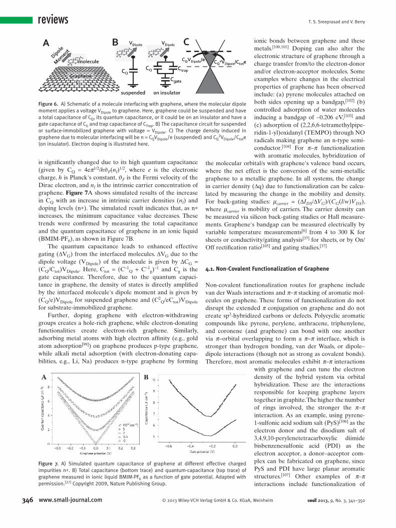
Figure 6 . A) Schematic of a molecule interfacing with graphene, where the molecular dipole moment applies a voltage V Dipole to graphene. Here, graphene could be suspended and have a total capacitance of C Q , its quantum capacitance, or it could be on an insulator and have a gate capacitance of C G and trap capacitance of C Trap . B) The capacitance circuit for suspended or surface-immobilized graphene with voltage = V Dipole . C) The charge density induced in graphene due to molecular interfacing will be n = C Q V Dipole /e (suspended) and C Q 2 V Dipole /C tot e (on insulator). Electron doping is illustrated here.
is signifi cantly changed due to its high quantum capacitance
(given by C Q = 4e π 1/2 / h ϑ F ( n l ) 1/2 , where e is the electronic
charge, h is Planck's constant, ϑ F is the Fermi velocity of the
Dirac electron, and n l is the intrinsic carrier concentration of
graphene. Figure 7 A shows simulated results of the increase
in C Q with an increase in intrinsic carrier densities ( n l ) and
doping levels (n ∗ ). The simulated result indicates that, as n ∗
increases, the minimum capacitance value decreases. These
trends were confi rmed by measuring the total capacitance
and the quantum capacitance of graphene in an ionic liquid
(BMIM-PF 6 ), as shown in Figure 7 B.
The quantum capacitance leads to enhanced effective
gating ( Δ V G ) from the interfaced molecules. Δ V G due to the
dipole voltage (V Dipole ) of the molecule is given by Δ C G =
(C Q /C tot )V Dipole . Here, C tot = (C − 1 Q + C − 1 g ) − 1 and C g is the
gate capacitance. Therefore, due to the quantum capaci-
tance in graphene, the density of states is directly amplifi ed
by the interfaced molecule's dipole moment and is given by
(C Q /e)V Dipole for suspended graphene and (C 2 Q /eC tot )V Dipole
for substrate-immobilized graphene.
Further, doping graphene with electron-withdrawing
groups creates a hole-rich graphene, while electron-donating
functionalities create electron-rich graphene. Similarly,
adsorbing metal atoms with high electron affi nity (e.g., gold
atom adsorption [ 99 ] ) on graphene produces p-type graphene,
while alkali metal adsorption (with electron-donating capa-
bilities, e.g., Li, Na) produces n-type graphene by forming
6 www.small-journal.com © 2013 Wiley-VCH Verlag GmbH & Co. KGaA,
Figure 7 . A) Simulated quantum capacitance of graphene at different effective charged impurities n ∗ . B) Total capacitance (bottom trace) and quantum-capacitance (top trace) of graphene measured in ionic liquid BMIM-PF 6 as a function of gate potential. Adapted with permission. [ 27 ] Copyright 2009, Nature Publishing Group.
ionic bonds between graphene and these
metals. [ 100 , 101 ] Doping can also alter the
electronic structure of graphene through a
charge transfer from/to the electron-donor
and/or electron-acceptor molecules. Some
examples where changes in the electrical
properties of graphene has been observed
include: (a) pyrene molecules attached on
both sides opening up a bandgap, [ 102 ] (b)
controlled adsorption of water molecules
inducing a bandgap of ∼ 0.206 eV, [ 103 ] and
(c) adsorption of (2,2,6,6-tetramethylpipe-
ridin-1-yl)oxidanyl (TEMPO) through NO
radicals making graphene an n-type semi-
conductor. [ 104 ] For π − π functionalization
with aromatic molecules, hybridization of
the molecular orbital/s with graphene's valence band occurs,
where the net effect is the conversion of the semi-metallic
graphene to a metallic graphene. In all systems, the change
in carrier density ( Δ q) due to functionalization can be calcu-
lated by measuring the change in the mobility and density.
For back-gating studies: μ carrier = ( Δ I DS / Δ V G )/( C G ( l / w ) V DS ),
where μ carrier is mobility of carriers. The carrier density can
be measured via silicon back-gating studies or Hall measure-
ments. Graphene's bandgap can be measured electrically by
variable temperature measurements [ 6 ] from 4 to 300 K for
sheets or conductivity/gating analysis [ 37 ] for sheets, or by On/
Off rectifi cation ratio [ 105 ] and gating studies. [ 37 ]
4.1. Non-Covalent Functionalization of Graphene
Non-covalent functionalization routes for graphene include
van der Waals interactions and π − π stacking of aromatic mol-
ecules on graphene. These forms of functionalization do not
disrupt the extended π conjugation on graphene and do not
create sp 3 -hybridized carbons or defects. Polycyclic aromatic
compounds like pyrene, perylene, anthracene, triphenylene,
and coronene (and graphene) can bond with one another
via π − orbital overlapping to form a π − π interface, which is
stronger than hydrogen bonding, van der Waals, or dipole–
dipole interactions (though not as strong as covalent bonds).
Therefore, most aromatic molecules exhibit π – π interactions
with graphene and can tune the electron
density of the hybrid system via orbital
hybridization. These are the interactions
responsible for keeping graphene layers
together in graphite. The higher the number
of rings involved, the stronger the π − π
interaction. As an example, using pyrene-
1-sulfonic acid sodium salt (PyS) [ 106 ] as the
electron donor and the disodium salt of
3,4,9,10-perylenetetracarboxylic diimide
bisbenzenesulfonic acid (PDI) as the
electron acceptor, a donor–acceptor com-
plex can be fabricated on graphene, since
PyS and PDI have large planar aromatic
structures. [ 107 ] Other examples of π – π
interactions include functionalization of
Weinheim small 2013, 9, No. 3, 341–350

Functionalization Effects on the Electrical Properties of Graphene
picket-fence porphyrin (FeTMAPP), [ 108 ] pyrenebutyrate, [ 109 ]
porphyrin (5,10,15,20-tetrakis(1-methyl-4-pyridinio)por-
phyrin (TMPyP)), [ 110 ] coronene carboxylate, [ 111 ] and poly-
oxyethylene sorbitan laurate. [ 112 ] Further adsorption-based
anchoring of polymers on graphene has been achieved
with ethyl cellulose, [ 113 ] 1,2-distearoyl-sn-glycero- 3-phos-
phoethanolamine- N -[methoxy(polyethyleneglycol)-5000]
(DSPE-mPEG) [ 114 ] and poly(m-phenylenevinyleneco-2,5-
dioctoxy-p-phenylenevinylene) (PmPV), [ 115 ] PMMA, [ 116 ]
poly(3-hexylthiophene-2,5-diyl) (P3HT) and poly[2-methoxy-
5-(2-ethylhexyloxy)-1,4-phenylenevinylene] (MEH-PPV). [ 117 ]
Here, the interfacing molecule's dipole moment and the
enhanced doping due to the high quantum capacitance of
graphene sensitively changes graphene's electrical proper-
ties. [ 118 ] Another example of non-covalent binding is that
between oxygen functionalities (named 'oxygen debris')
and the sp 2 lattice region of GO. Here, the oxygen can be
detached under basic conditions. [ 119 ]
4.2. Gas Adsorption
Gas molecules adsorbed on graphene induce a signifi cant
change in its electrical behavior. Adsorption of NO, NO 2 ,
NH 3 , H 2 O, H 2 , and CO [ 120–125 ] molecules can act as donors or
acceptors, resulting in sensitive doping and changes to graph-
ene’s electrical conductivity. Graphene—being a perfect 2D
crystalline material which can be considered as having only
a surface and no volume, with exceptional conductivity even
in the limit of zero carrier density—will have signifi cant fl uc-
tuations in relative carrier concentration by the addition of
a few extra electrons. [ 120 , 121 , 125–129 ] This molecular doping can
follow two charge-transfer mechanisms: (a) charge transfer
can happen depending upon the relative positions of the
highest occupied molecular orbital (HOMO) and lowest
unoccupied molecular orbital (LUMO) of the adsorbate
with respect to the Fermi level of graphene in the density
of states. If the Fermi level of pristine graphene is below the
HOMO of the adsorbate in density of states, there is a charge
transfer towards graphene. However, if the Fermi level of
graphene is close to the LUMO of the adsorbate which is
situated below the Fermi level, the charge transfer will be
towards the adsorbate molecule; (b) the orbital hybridization
of the HOMO and LUMO with graphene can also infl uence
the charge-transfer process. There is an inverse relationship
between energy difference between the interacting orbital
and the extent of hybridization.
5. Integrated Model for Mechanism
Based on the review above, we propose three fundamental
mechanisms (or effects) of functionalization, which affect
the electrical properties of graphene post functionalization.
These are (a) conversion of the basal carbon's hybridiza-
tion state (sp 2 to sp 3 ), which distorts the lattice, disrupts the
potential continuum, enhances electron–hole puddles, and
changes the density of electronic states; (b) interaction of the
dipole moment of the functionalizing/interfacing molecules
© 2013 Wiley-VCH Verlag Gmbsmall 2013, 9, No. 3, 341–350
with graphene, which leads to enhanced doping due to
quantum capacitance, increase in electron–hole puddles, and
disruption of the potential continuum, and; (c) molecular
orbital hybridization with graphene's electronic bands. For
covalent functionalization, the electrical properties are infl u-
enced by all of the above three mechanisms. For molecular
adsorption and aromatic π − π interactions, a combination of
mechanisms (b) and (c) occurs. Two other functionalization
schemes which affect electrical properties are (1) introduc-
tion of defects, and (2) lattice incorporation. The defect acts
as a carrier-defi cient center and lattice-distortion site, which
causes scattering (similar to the mechanism (a) mentioned
above). The lattice incorporation of a dopant might not
create a lattice distortion; however, it will lead to breakage
of the potential continuum and enhanced electron–hole
puddles, which will lead to enhanced scattering. The dopant
polarity is governed by the bonding mechanism, molecular
dipole moment, and its electronegativity; the mobility is gov-
erned by functionalization density, electronegativity (creation
of an electron–hole puddle), the bonding/interfacing mecha-
nism (lattice distortion and potential continuum), and sp 2 /sp 3
domain sizes; and the transport mechanism is governed by
sp 2 /sp 3 domain-size distribution, and the bonding/interfacing
mechanism (potential barrier for transport and electron–
hole puddle distribution). The same mechanism can describe
the electrical properties of graphene/nanoparticle hybrids as
well. [ 130–132 ]
6. Future Scope for Research
While graphene functionalization has gained signifi cant atten-
tion, relatively limited knowledge is available on the effect
of functionalization on sandwiched graphene sheets, such
as graphene bilayers with only one layer functionalized or
graphene trilayers with both outer layers functionalized. Here,
it is expected that the electrical properties will be infl uenced
by π − π bonding, orbital hybridization, and quantum-capac-
itance-induced doping (via dipole moments from the func-
tionalized layer), however, experimental evidence is required.
Importantly, the electron–hole puddle-induced scattering will
have to be studied. It is important to note that such structures
are challenging to fabricate and control. Another category of
graphenic materials gaining attention is graphene nanostruc-
tures, such as graphene quantum dots (GQDs) and graphene
nanoribbons (GNRs) which, due to quantum confi nement
( < 100 nm for GQDs and < 50 nm for GNRs) and edge states,
open a bandgap. For these nanostructures, it is important to
study the combined effects of quantum confi nement and func-
tionalization on their band structure. Further, the dimensions
of the electron or hole puddles (usually several micrometers
in graphene), if any, in these nanostructures will have to be
evaluated, especially for GNRs, which are considered to be
the ideal graphene-based material for transistors.
A recent study showed that functionalization on graphene
depends on the electron–hole puddles, which can signifi -
cantly alter both the Fermi level and the scattering-center
density to produce multifunctional graphene sheets. [ 133 ] Such
multifunctional sheets with organized functionalized and
347www.small-journal.comH & Co. KGaA, Weinheim

T. S. Sreeprasad and V. Berry
348
reviews
non-functionalized domains need to be studied for their elec-tronic transport properties. Similarly, graphene/boron-nitride
hetrostructures also need to be studied for their electrical
transport properties. Further, there is scope to conduct
detailed studies on the creation of electron–hole puddles on
graphene as a consequence of molecular interfacing and func-
tionalization. These could be scanning tunneling microscopy
(STM) experiments, which can locate the molecular attach-
ment site and map the electron–hole puddles around the site.
7. Summary
This review outlines a detailed and integrated model to
explain the factors infl uencing the electrical properties of
functionalized graphene (covalent bonding, adsorption,
π − π interactions, and lattice incorporation). The model
explains that the electrical properties are governed via three
mechanisms: (a) conversion of the sp 2 -hybridized state to
sp 3 , (b) molecular dipole interactions and the associated
quantum-capacitance-enhanced doping, and (c) hybridization
of molecular orbitals with graphene's electronic bands. Also,
graphene trilayers with outer layers functionalized, graphene
quantum structures, and multi-functionalized graphene are
identifi ed as upcoming graphenic materials where further
functionalization/electrical studies are required.
Acknowledgements
VB thanks the fi nancial support from NSF (CMMI-1054877, CMMI-0939523 and CMMI-1030963), Offi ce of Naval Research (grant-N000141110767), Terry C. Johnson Center for Basic Cancer Research, and KSU start-up.
[ 1 ] K. S. Novoselov , A. K. Geim , S. V. Morozov , D. Jiang , Y. Zhang , S. V. Dubonos , I. V. Grigorieva , A. A. Firsov , Science 2004 , 306 , 666 .
[ 2 ] K. S. Novoselov , E. McCann , S. V. Morozov , V. I. Fal’ko , M. I. Katsnelson , U. Zeitler , D. Jiang , F. Schedin , A. K. Geim , Nat. Phys. 2006 , 2 , 177 .
[ 3 ] K. S. Novoselov , A. K. Geim , S. V. Morozov , D. Jiang , M. I. Katsnelson , I. V. Grigorieva , S. V. Dubonos , A. A. Firsov , Nature 2005 , 438 , 197 .
[ 4 ] K. S. Novoselov , D. Jiang , F. Schedin , T. J. Booth , V. V. Khotkevich , S. V. Morozov , A. K. Geim , Proc. Natl. Acad. Sci. USA 2005 , 102 , 10451 .
[ 5 ] M. H. Gass , U. Bangert , A. L. Bleloch , P. Wang , R. R. Nair , A. K. Geim , Nat. Nanotechnol. 2008 , 3 , 676 .
[ 6 ] X. Du , I. Skachko , A. Barker , E. Y. Andrei , Nat. Nanotechnol. 2008 , 3 , 491 .
[ 7 ] J. H. Chen , C. Jang , S. D. Xiao , M. Ishigami , M. S. Fuhrer , Nat. Nanotechnol. 2008 , 3 , 206 .
[ 8 ] A. Akturk , N. Goldsman , J. Appl. Phys. 2008 , 103 , 053702 . [ 9 ] R. R. Nair , P. Blake , A. N. Grigorenko , K. S. Novoselov ,
T. J. Booth , T. Stauber , N. M. R. Peres , A. K. Geim , Science 2008 , 320 , 1308 .
[ 10 ] A. A. Balandin , S. Ghosh , W. Bao , I. Calizo , D. Teweldebrhan , F. Miao , C. N. Lau , Nano Lett. 2008 , 8 , 902 .
www.small-journal.com © 2013 Wiley-VCH Ve
[ 11 ] C. Lee , X. D. Wei , J. W. Kysar , J. Hone , Science 2008 , 321 , 385 . [ 12 ] N. Mohanty , V. Berry , Nano Lett. 2008 , 8 , 4469 . [ 13 ] F. Schedin , A. K. Geim , S. V. Morozov , E. W. Hill , P. Blake ,
M. I. Katsnelson , K. S. Novoselov , Nat. Mater. 2007 , 6 , 652 . [ 14 ] J. Liu , J. Tang , J. J. Gooding , J. Mater. Chem. 2012 , 22 , 12435 . [ 15 ] X. Huang , Z. Yin , S. Wu , X. Qi , Q. He , Q. Zhang , Q. Yan , F. Boey ,
H. Zhang , Small 2011 , 7 , 1876 . [ 16 ] W. Wei , X. Qu , Small 2012 , 8 , 2138 . [ 17 ] Z. Sun , D. K. James , J. M. Tour , J. Phys. Chem. Lett. 2011 , 2 , 2425 . [ 18 ] C. N. R. Rao , K. S. Subrahmanyam , H. S. S. Ramakrishna Matte ,
A. Govindaraj , Mod. Phys. Lett. B 2011 , 25 , 427 . [ 19 ] T. S. Sreeprasad , T. Pradeep , Int. J. Mod. Phys. B 2012 , 26 ,
1242001 . [ 20 ] X. Huang , Z. Yin , S. Wu , X. Qi , Q. He , Q. Zhang , Q. Yan , F. Boey ,
H. Zhang , Small 2011 , 7 , 1876 . [ 21 ] O. C. Compton , S. T. Nguyen , Small 2010 , 6 , 711 . [ 22 ] L. Yan , Y. B. Zheng , F. Zhao , S. Li , X. Gao , B. Xu , P. S. Weiss ,
Y. Zhao , Chem. Soc. Rev. 2012 , 41 , 97 . [ 23 ] T. M. Swager , ACS Macro Lett. 2011 , 1 , 3 . [ 24 ] J. G. S. Elton , New J. Phys. 2012 , 14 , 043022 . [ 25 ] D. C. Elias , R. R. Nair , T. M. G. Mohiuddin , S. V. Morozov , P. Blake ,
M. P. Halsall , A. C. Ferrari , D. W. Boukhvalov , M. I. Katsnelson , A. K. Geim , K. S. Novoselov , Science 2009 , 323 , 610 .
[ 26 ] P. Nguyen , V. Berry , J. Phys. Chem. Lett. 2012 , 3 , 1024 . [ 27 ] J. Xia , F. Chen , J. Li , N. Tao , Nat. Nanotechnol. 2009 , 4 , 505 . [ 28 ] S.-J. Sun , C.-Y. Lin , Europhys. Lett. 2011 , 96 , 10002 . [ 29 ] D. Wei , Y. Liu , Y. Wang , H. Zhang , L. Huang , G. Yu , Nano Lett.
2009 , 9 , 1752 . [ 30 ] G. Eda , Y. Y. Lin , C. Mattevi , H. Yamaguchi , H. A. Chen , I. S. Chen ,
C. W. Chen , M. Chhowalla , Adv. Mater. 2010 , 22 , 505 . [ 31 ] N. Mohanty , D. Moore , Z. Xu , T. S. Sreeprasad , A. Nagaraja ,
A. A. Rodriguez , V. Berry , Nat. Commun. 2012 , 3 , 844 . [ 32 ] I. Jung , D. A. Dikin , R. D. Piner , R. S. Ruoff , Nano Lett. 2008 , 8 ,
4283 . [ 33 ] A. Cortijo , M. A. H. Vomediano , Nuclear Phys. B 2007 , 763 , 293 . [ 34 ] A. B. Kaiser , C. Gomez-Navarro , R. S. Sundaram , M. Burghard ,
K. Kern , Nano Lett. 2009 , 9 , 1787 . [ 35 ] T. Jayasekera , J. W. Mintmire , Int. J. Quantum Chem. 2007 , 107 ,
3071 . [ 36 ] K. Jasuja , V. Berry , ACS Nano 2009 , 3 , 2358 . [ 37 ] M. Y. Han , B. Ozyilmaz , Y. B. Zhang , P. Kim , Phys. Rev. Lett. 2007 ,
98 , 206805 . [ 38 ] M. I. Katsnelson , K. S. Novoselov , A. K. Geim , Nat. Phys. 2006 ,
2 , 620 . [ 39 ] P. Huang , L. Jing , H. R. Zhu , X. Y. Gao , J. Phys.: Condens. Matter
2012 , 24 , 235305 . [ 40 ] J. Martin , N. Akerman , G. Ulbricht , T. Lohmann , J. H. Smet ,
K. von Klitzing , A. Yacoby , Nat. Phys. 2008 , 4 , 144 . [ 41 ] Q. H. Wang , Z. Jin , K. K. Kim , A. J. Hilmer , G. L. C. Paulus ,
C. J. Shih , M. H. Ham , J. D. Sanchez-Yamagishi , K. Watanabe , T. Taniguchi , J. Kong , P. Jarillo-Herrero , M. S. Strano , Nat. Chem. 2012 , 4 , 724 .
[ 42 ] W. S. Hummers , R. E. Offeman , J. Am. Chem. Soc. 1958 , 80 , 1339 .
[ 43 ] W. Gao , L. B. Alemany , L. Ci , P. M. Ajayan , Nat. Chem. 2009 , 1 , 403 .
[ 44 ] D. R. Dreyer , S. Park , C. W. Bielawski , R. S. Ruoff , Chem. Soc. Rev. 2010 , 39 , 228 .
[ 45 ] B. C. Brodie , Phil. Trans. R. Soc. London 1859 , 149 , 249 . [ 46 ] M. Trömel , M. Russ , Angew. Chem. 1987 , 99 , 1037 . [ 47 ] A. B. Bourlinos , D. Gournis , D. Petridis , T. Szabó , A. Szeri ,
I. Dékány , Langmuir 2003 , 19 , 6050 . [ 48 ] J. R. Lomeda , C. D. Doyle , D. V. Kosynkin , W. F. Hwang , J. M. Tour ,
J. Am. Chem. Soc. 2008 , 130 , 16201 . [ 49 ] S. Niyogi , E. Bekyarova , M. E. Itkis , J. L. McWilliams ,
M. A. Hamon , R. C. Haddon , J. Am. Chem. Soc. 2006 , 128 , 7720 .
rlag GmbH & Co. KGaA, Weinheim small 2013, 9, No. 3, 341–350

Functionalization Effects on the Electrical Properties of Graphene
[ 50 ] Z. Liu , J. T. Robinson , X. Sun , H. Dai , J. Am. Chem. Soc. 2008 , 130 , 10876 .
[ 51 ] X. D. Zhuang , Y. Chen , G. Liu , P. P. Li , C. X. Zhu , E. T. Kang , K. G. Noeh , B. Zhang , J. H. Zhu , Y. X. Li , Adv. Mater. 2010 , 22 , 1731 .
[ 52 ] Y. Xu , Z. Liu , X. Zhang , Y. Wang , J. Tian , Y. Huang , Y. Ma , X. Zhang , Y. Chen , Adv. Mater. 2009 , 21 , 1275 .
[ 53 ] J. Shen , B. Yan , M. Shi , H. Ma , N. Li , M. Ye , J. Colloid Interface Sci. 2011 , 356 , 543 .
[ 54 ] N. Mohanty , V. Berry , Nano Lett. 2008 , 8 , 4469 . [ 55 ] N. Mohanty , M. Fahrenholtz , A. Nagaraja , D. Boyle , V. Berry ,
Nano Lett. 2011 , 11 , 1270 . [ 56 ] S. Stankovich , D. A. Dikin , G. H. B. Dommett , K. M. Kohlhaas ,
E. J. Zimney , E. A. Stach , R. D. Piner , S. T. Nguyen , R. S. Ruoff , Nature 2006 , 442 , 282 .
[ 57 ] D. D. Zhang , S. Z. Zu , B. H. Han , Carbon 2009 , 47 , 2993 . [ 58 ] C. Xu , X. Wu , J. Zhu , X. Wang , Carbon 2008 , 46 , 386 . [ 59 ] C. Xu , X. Wang , J. Wang , H. Hu , L. Wan , Chem. Phys. Lett. 2010 ,
498 , 162 . [ 60 ] H. J. Salavagione , M. ü. A. Gómez , G. Martínez , Macromolecules
2009 , 42 , 6331 . [ 61 ] Y. Matsuo , T. Tabata , T. Fukunaga , T. Fukutsuka , Y. Sugie , Carbon
2005 , 43 , 2875 . [ 62 ] T. Kuila , S. Bose , C. E. Hong , M. E. Uddin , P. Khanra , N. H. Kim ,
J. H. Lee , Carbon 2011 , 49 , 1033 . [ 63 ] J. Shen , M. Shi , H. Ma , B. Yan , N. Li , Y. Hu , M. Ye , J. Colloid Inter-
face Sci. 2010 , 352 , 366 . [ 64 ] M. C. Hsiao , S. H. Liao , M. Y. Yen , P. I. Liu , N. W. Pu , C. A. Wang ,
C. C. Ma , ACS Appl. Mater. Interfaces 2010 , 2 , 3092 . [ 65 ] G. Wang , B. Wang , J. Park , J. Yang , X. Shen , J. Yao , Carbon 2009 ,
47 , 68 . [ 66 ] C. Shan , H. Yang , D. Han , Q. Zhang , A. Ivaska , L. Niu , Langmuir
2009 , 25 , 12030 . [ 67 ] X. Sun , Z. Liu , K. Welsher , J. Robinson , A. Goodwin , S. Zaric ,
H. Dai , Nano Res. 2008 , 1 , 203 . [ 68 ] L. Q. Xu , W. J. Yang , K. G. Neoh , E. T. Kang , G. D. Fu , Macromol-
ecules 2010 , 43 , 8336 . [ 69 ] T. A. Pham , N. A. Kumar , Y. T. Jeong , Synthetic Metals 2010 , 160 ,
2028 . [ 70 ] S. M. Kang , S. Park , D. Kim , S. Y. Park , R. S. Ruoff , H. Lee , Adv.
Funct. Mater. 2011 , 21 , 108 . [ 71 ] T. Kuila , P. Khanra , S. Bose , N. H. Kim , B.-C. Ku , B. Moon ,
J. H. Lee , Nanotechnology 2011 , 22 , 305710 . [ 72 ] H. Yang , F. Li , C. Shan , D. Han , Q. Zhang , L. Niu , A. Ivaska , J.
Mater. Chem. 2009 , 19 , 4632 . [ 73 ] H. Yang , C. Shan , F. Li , D. Han , Q. Zhang , L. Niu , Chem. Commun.
2009 , 3880 . [ 74 ] B. K. Ahn , J. Sung , Y. Li , N. Kim , M. Ikenberry , K. Hohn ,
N. Mohanty , P. Nguyen , T. S. Sreeprasad , S. Kraft , V. Berry , X. S. Sun , Adv. Mater. 2012 , 24 , 2123 .
[ 75 ] E. Bekyarova , M. E. Itkis , P. Ramesh , C. Berger , M. Sprinkle , W. A. de Heer , R. C. Haddon , J. Am. Chem. Soc. 2009 , 131 , 1336 .
[ 76 ] Z. Sun , S. i. Kohama , Z. Zhang , J. Lomeda , J. Tour , Nano Res. 2010 , 3 , 117 .
[ 77 ] Y. Si , E. T. Samulski , Nano Lett. 2008 , 8 , 1679 . [ 78 ] Y. Zhu , A. L. Higginbotham , J. M. Tour , Chem. Mater. 2009 , 21 ,
5284 . [ 79 ] M. Fang , K. Wang , H. Lu , Y. Yang , S. Nutt , J. Mater. Chem. 2009 ,
19 , 7098 . [ 80 ] V. H. Pham , T. V. Cuong , S. H. Hur , E. Oh , E. J. Kim , E. W. Shin ,
J. S. Chung , J. Mater. Chem. 2011 , 21 , 3371 . [ 81 ] S. Sarkar , E. Bekyarova , R. C. Haddon , Acc. Chem. Res. 2012 ,
45 , 673 . [ 82 ] V. Georgakilas , A. B. Bourlinos , R. Zboril , T. A. Steriotis ,
P. Dallas , A. K. Stubos , C. Trapalis , Chem. Commun. 2010 , 46 , 1766 .
© 2013 Wiley-VCH Verlag GmbHsmall 2013, 9, No. 3, 341–350
[ 83 ] M. Quintana , K. Spyrou , M. Grzelczak , W. R. Browne , P. Rudolf , M. Prato , ACS Nano 2010 , 4 , 3527 .
[ 84 ] J. Choi , K. j. Kim , B. Kim , H. Lee , S. Kim , J. Phys. Chem. C 2009 , 113 , 9433 .
[ 85 ] X. Xu , Q. Luo , W. Lv , Y. Dong , Y. Lin , Q. Yang , A. Shen , D. Pang , J. Hu , J. Qin , Z. Li , Macromol. Chem. Phys. 2011 , 212 , 768 .
[ 86 ] X. Zhong , J. Jin , S. Li , Z. Niu , W. Hu , R. Li , J. Ma , Chem. Commun. 2010 , 46 , 7340 .
[ 87 ] S. P. Economopoulos , G. Rotas , Y. Miyata , H. Shinohara , N. Tagmatarchis , ACS Nano 2010 , 4 , 7499 .
[ 88 ] S. Vadukumpully , J. Gupta , Y. Zhang , G. Q. Xu , S. Valiyaveettil , Nanoscale 2011 , 3 , 303 .
[ 89 ] S. Lebegue , M. Klintenberg , O. Eriksson , M. I. Katsnelson , Phys. Rev. B 2009 , 79 , 245117 .
[ 90 ] R. Balog , B. Jorgensen , L. Nilsson , M. Andersen , E. Rienks , M. Bianchi , M. Fanetti , E. Laegsgaard , A. Baraldi , S. Lizzit , Z. Sljivancanin , F. Besenbacher , B. Hammer , T. G. Pedersen , P. Hofmann , L. Hornekaer , Nat. Mater. 2010 , 9 , 315 .
[ 91 ] J. T. Robinson , J. S. Burgess , C. E. Junkermeier , S. C. Badescu , T. L. Reinecke , F. K. Perkins , M. K. Zalalutdniov , J. W. Baldwin , J. C. Culbertson , P. E. Sheehan , E. S. Snow , Nano Lett. 2010 , 10 , 3001 .
[ 92 ] R. R. Nair , W. Ren , R. Jall , I. Riaz , V. G. Kravets , L. Britnell , P. Blake , F. Schedin , A. S. Mayorov , S. Yuan , M. I. Katsnelson , H. M. Cheng , W. Strupinski , L. G. Bulusheva , A. V. Okotrub , I. V. Grigorieva , A. N. Grigorenko , K. S. Novoselov , A. K. Geim , Small 2010 , 6 , 2877 .
[ 93 ] S. H. Cheng , K. Zou , F. Okino , H. R. Gutierrez , A. Gupta , N. Shen , P. C. Eklund , J. O. Sofo , J. Zhu , Phys. Rev. B 2010 , 81 , 205435 .
[ 94 ] B. Li , L. Zhou , D. Wu , H. Peng , K. Yan , Y. Zhou , Z. Liu , ACS Nano 2011 , 5 , 5957 .
[ 95 ] J. Wu , L. Xie , Y. Li , H. Wang , Y. Ouyang , J. Guo , H. Dai , J. Am. Chem. Soc. 2011 , 133 , 19668 .
[ 96 ] G. Imamura , K. Saiki , J. Phys. Chem. C 2011 , 115 , 10000 . [ 97 ] B. Guo , Q. Liu , E. Chen , H. Zhu , L. Fang , J. R. Gong , Nano Lett.
2010 , 10 , 4975 . [ 98 ] T. Wu , H. Shen , L. Sun , B. Cheng , B. Liu , J. Shen , New J. Chem.
2012 , 36 , 1385 . [ 99 ] I. Gierz , C. Riedl , U. Starke , C. R. Ast , K. Kern , Nano Lett. 2008 ,
8 , 4603 . [ 100 ] A. Bostwick , T. Ohta , T. Seyller , K. Horn , E. Rotenberg , Nat. Phys.
2007 , 3 , 36 . [ 101 ] T. Ohta , A. Bostwick , T. Seyller , K. Horn , E. Rotenberg , Science
2006 , 313 , 951 . [ 102 ] D. M. Chen , P. M. Shenai , Y. Zhao , Phys. Chem. Chem. Phys.
2011 , 13 , 1515 . [ 103 ] F. Yavari , C. Kritzinger , C. Gaire , L. Song , H. Gulapalli ,
T. Borca-Tasciuc , P. M. Ajayan , N. Koratkar , Small 2010 , 6 , 2535 .
[ 104 ] H. Lee , S. Yang , J. Choi , Y. Park , S. Kim , J. Phys. Chem. C 2011 , 115 , 18736 .
[ 105 ] X. L. Li , X. R. Wang , L. Zhang , S. W. Lee , H. J. Dai , Science 2008 , 319 , 1229 .
[ 106 ] Y. Xu , H. Bai , G. Lu , C. Li , G. Shi , J. Am. Chem. Soc. 2008 , 130 , 5856 .
[ 107 ] Q. Su , S. Pang , V. Alijani , C. Li , X. Feng , K. Müllen , Adv. Mater. 2009 , 21 , 3191 .
[ 108 ] W. Tu , J. Lei , S. Zhang , H. Ju , Chem. Eur. J. 2010 , 16 , 10771 . [ 109 ] Y. Xu , H. Bai , G. Lu , C. Li , G. Shi , J. Am. Chem. Soc. 2008 , 130 ,
5856 . [ 110 ] Y. Xu , L. Zhao , H. Bai , W. Hong , C. Li , G. Shi , J. Am. Chem. Soc.
2009 , 131 , 13490 . [ 111 ] A. Ghosh , K. V. Rao , S. George , C. N. R. Rao , Chem. Eur. J. 2010 ,
16 , 2700 . [ 112 ] S. Park , N. Mohanty , J. W. Suk , A. Nagaraja , J. An , R. D. Piner ,
W. Cai , D. R. Dreyer , V. Berry , R. S. Ruoff , Adv. Mater. 2010 , 22 , 1736 .
349www.small-journal.com & Co. KGaA, Weinheim

T. S. Sreeprasad and V. Berry
350
reviews
[ 113 ] Y. T. Liang , M. C. Hersam , J. Am. Chem. Soc. 2010 , 132 , 17661 . [ 114 ] X. Li , G. Zhang , X. Bai , X. Sun , X. Wang , E. Wang , H. Dai , Nat.Nanotechnol. 2008 , 3 , 538 . [ 115 ] X. Li , X. Wang , L. Zhang , S. Lee , H. Dai , Science 2008 , 319 ,
1229 . [ 116 ] T. Ramanathan , A. A. Abdala , S. Stankovich , D. A. Dikin ,
M. Herrera-Alonso , R. D. Piner , D. H. Adamson , H. C. Schniepp , X. Chen , R. S. Ruoff , S. T. Nguyen , I. A. Aksay , R. K. Prud’homme , L. C. Brinson , Nat. Nanotechnol. 2008 , 3 , 327 .
[ 117 ] Y. Wang , D. Kurunthu , G. W. Scott , C. J. Bardeen , J. Phys. Chem. C 2010 , 114 , 4153 .
[ 118 ] M. Kim , N. S. Safron , C. Huang , M. S. Arnold , P. Gopalan , Nano Lett. 2011 , 12 , 182 .
[ 119 ] J. P. Rourke , P. A. Pandey , J. J. Moore , M. Bates , I. A. Kinloch , R. J. Young , N. R. Wilson , Angew. Chem. Int. Ed. 2011 , 50 , 3173 .
[ 120 ] F. Schedin , A. K. Geim , S. V. Morozov , E. W. Hill , P. Blake , M. I. Katsnelson , K. S. Novoselov , Nat. Mater. 2007 , 6 , 652 .
[ 121 ] M. Gautam , A. H. Jayatissa , Mater. Sci. Engin. C 2011 , 31 , 1405 .
[ 122 ] I. Jung , D. Dikin , S. Park , W. Cai , S. L. Mielke , R. S. Ruoff , J. Phys. Chem. C 2008 , 112 , 20264 .
[ 123 ] G. H. Lu , L. E. Ocola , J. H. Chen , Appl. Phys. Lett. 2009 , 94 , 083111 .
[ 124 ] M. Qazi , T. Vogt , G. Koley , Appl. Phys. Lett. 2007 , 91 .
www.small-journal.com © 2013 Wiley-VCH V
[ 125 ] H. Sukju , H. C. Joon , L. Juwhan , K. K. Whan , S. Hyunjin , J. Y. Choi , J. H. Choi , Y. L. Sang , J. M. Kim , H. K. Jae , L. Seok , C. J. Seong , presented at Nanotechnology Materials and Devices Conference (NMDC), 2010 IEEE.
[ 126 ] S. Rumyantsev , G. Liu , M. S. Shur , R. A. Potyrailo , A. A. Balandin , Nano Lett. 2012 , 12 , 2294 .
[ 127 ] J. D. Fowler , M. J. Allen , V. C. Tung , Y. Yang , R. B. Kaner , B. H. Weiller , ACS Nano 2009 , 3 , 301 .
[ 128 ] F. Yavari , Z. Chen , A. V. Thomas , W. Ren , H. M. Cheng , N. Koratkar , Sci. Rep. 2011 , 1 .
[ 129 ] G. Lu , S. Park , K. Yu , R. S. Ruoff , L. E. Ocola , D. Rosenmann , J. Chen , ACS Nano 2011 , 5 , 1154 .
[ 130 ] G. Konstantatos , M. Badioli , L. Gaudreau , J. Osmond , M. Bernechea , F. P. G. de Arquer , F. Gatti , F. H. L. Koppens , Nat. Nanotechnol. 2012 , 7 , 363 .
[ 131 ] D. Zhang , L. Gan , Y. Cao , Q. Wang , L. Qi , X. Guo , Adv. Mater. 2012 , 24 , 2715 .
[ 132 ] Z. Fang , Z. Liu , Y. Wang , P. M. Ajayan , P. Nordlander , N. J. Halas , Nano Lett. 2012 , 12 , 3808 .
[ 133 ] Q. H. Wang , Z. Jin , K. K. Kim , A. J. Hilmer , G. L. C. Paulus , C. J. Shih , M. H. Ham , J. D. Sanchez-Yamagishi , K. Watanabe , T. Taniguchi , J. Kong , P. Jarillo-Herrero , M. S. Strano , Nat. Chem. 2012 , 4 , 724 .
Received: September 6, 2012Published online: November 21, 2012
erlag GmbH & Co. KGaA, Weinheim small 2013, 9, No. 3, 341–350