holtek i/o 8-bit mtp starter kit user's guide
TRANSCRIPT

Holtek I/O 8-Bit MTP Starter Kit
User�s Guide October 2005
Copyright � 2005 by HOLTEK SEMICONDUCTOR INC. All rights reserved. Printed in Taiwan. No part of
this publication may be reproduced, stored in a retrieval system, or transmitted in any form by any means,
electronic, mechanical photocopying, recording, or otherwise without the prior written permission of
HOLTEK SEMICONDUCTOR INC.

NOTICE
The information appearing in this User�s Guide is believed to be accurate at the time of publication. How-
ever, Holtek assumes no responsibility arising from the use of the specifications described. The applica-
tions mentioned herein are used solely for the purpose of illustration and Holtek makes no warranty or
representation that such applications will be suitable without further modification, nor recommends the use
of its products for application that may present a risk to human life due to malfunction or otherwise. Holtek�s
products are not authorized for use as critical components in life support devices or systems. Holtek re-
serves the right to alter its products without prior notification. For the most up-to-date information, please
visit our web site at http://www.holtek.com.tw.

Contents
Chapter 1 Getting Starter .............................................................1
Introduction.....................................................................................................................1
Features...........................................................................................................................1
Starter Kit Contents........................................................................................................1
Install the MTP Starter Kit ..............................................................................................2
Run the Starter Kit Built-in Sample...............................................................................8
Run the Starter Kit Tutorial Program ..........................................................................11
Menus and Commands of the MTP Starter Kit Utility................................................13
Chapter 2 Tutorial Programs......................................................17
Tutorial 1: Buzzer..........................................................................................................17
Tutorial 2: Key Matrix Scan..........................................................................................19
Tutorial 3: Timer Display ..............................................................................................21
Tutorial 4: EEPROM Data Memory Processing ..........................................................23
Tutorial 5: Melody .........................................................................................................31
Contents
i

Chapter 3 Modify the Tutorial Programs...................................35
Build a New Project for Tutorial Programs.................................................................35
Set the DIP Switch for the Clock Source ....................................................................36
Configuration Option Table .........................................................................................36
Chapter 4 Target Board ..............................................................37
Chapter 5 Instruction Definition .................................................43
ii
Contents

C h a p t e r 1
Getting Starter
Introduction
The MTP (Multi-Time Programmable) Starter Kit helps in understanding the Holtek�s I/O 8-Bit
MTP microcontroller providing a quick, easy and low-cost way of instruction. It can also serve
as an MTP programmer and demonstration board.
Features
� Simple printed circuit board
� Can be connected to the PC�s USB port for communication
� Easy to use MTP Starter Kit software utility
� Tutorial programs for applications which can be easily modified
� Supports different MTP microcontrollers
Starter Kit Contents
� MTP Starter Kit Printed Circuit Board (PCB)
� USB cable
� CD-ROM with HT-IDE3000 and Starter Kit Utility
� User�s Manual
Chapter 1 Getting Starter
1
1

Install the MTP Starter Kit
Insert the HT-IDE3000 CD into the CD ROM drive, Fig 1-1 will be shown.
Fig 1-1
2
Holtek I/O 8-Bit MTP Starter Kit User�s Guide

Click the <Setup MTP Starter Kit> button and Fig 1-2 will be shown.
Fig 1-2
Chapter 1 Getting Starter
3

Specify the path you want to install the MTP starter Kit in Fig 1-3 and click the <Next> button.
Fig 1-3
4
Holtek I/O 8-Bit MTP Starter Kit User�s Guide

Then specify the shortcut name which will be inserted into the Program Group of the Start
Menu in Fig 1-4.
Fig 1-4
Chapter 1 Getting Starter
5
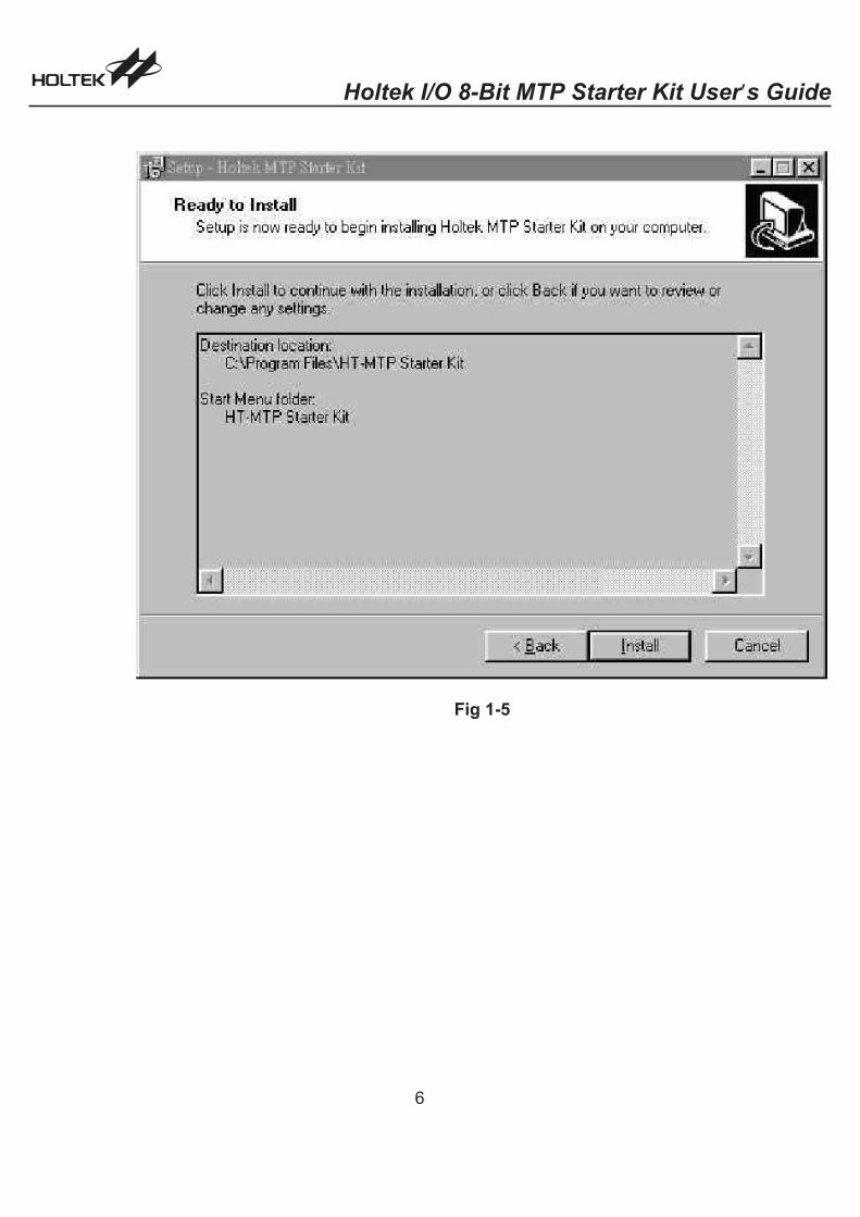
Fig 1-5
6
Holtek I/O 8-Bit MTP Starter Kit User�s Guide

In Fig 1-5, press the <Install> button to start installing. All the corresponding files will be cop-
ied to the specified destination location. If the process is successful, Fig 1-6 will be shown.
Press the <Finish> button and you can run MTP Starter Kit utility now.
Fig 1-6
Chapter 1 Getting Starter
7

Run the Starter Kit Built-in Sample
Connect the MTP Starter Kit PCB to the USB port of the PC using the USB cable, then the
sample program residing in the MTP microcontroller will be executed automatically.
The LEDs light up one by one and the two 7-segment displays will show the count number.
The built-in sample program will be erased when you download other tutorial program into
MTP microcontroller. The file LIGHT.MTP is the built-in sample program, which you can down-
load it again for demonstration.
If the PC system is Win95/98 and no USB driver is installed, then Fig 1-7 Will be displayed,
press the <Next> button.
Fig 1-7
8
Holtek I/O 8-Bit MTP Starter Kit User�s Guide

Fig 1-8 will be displayed, select the �Search the best driver for your device�, press the <Next>
button.
Fig 1-8
Chapter 1 Getting Starter
9

Fig 1-9 will be displayed. Select the �CD-ROM drive� and insert the Win98 System CD into
the CD-ROM, then press <Next> button and follow the instructions to install the driver.
Fig 1-9
10
Holtek I/O 8-Bit MTP Starter Kit User�s Guide

Run the Starter Kit Tutorial Program
Click the Start button, select Program and select MTP Starter Kit. Then the main window will
be displayed as shown in Fig 1-10
Fig 1-10
Select the File menu/Open command to open a tutorial file (e.g. CLOCK.MTP). The contents
of the file are displayed as shown in Fig 1-11. The left side of the window is the binary code of
the program and the right side is the data to be written to the Data EEPROM.
Chapter 1 Getting Starter
11

Fig 1-11
� Select the Download menu/ALL command as shown in Fig 1-12. This will download the
program code and data to the corresponding memory of the MTP microcontroller
HT48E50.
Fig 1-12
� When the download has started, a progress bar indicates the download percentage.
Press the reset button to run the tutorial program when the download is complete.
12
Holtek I/O 8-Bit MTP Starter Kit User�s Guide

Menus and Commands of the MTP Starter Kit Utility
There are a total of seven menus, File, Edit, View, Upload, Download, Tools and Help which
are described below.
Menu � File
The file menu provides file processing commands as follows:
� Open
Open an existing file with file extension name .MTP. This command will close the currently
opened file automatically before opening the specified file.
� Save
Write the active windows data to the active file.
� Save As...
Write the active windows data to the specified file.
� Select MCU Type
Select the MTP MCU type from the list box. If an MTP file has been opened already, then
the MCU type specified by this MTP file is selected in the list box. Otherwise, the default
MCU type is selected. User can select an MCU type which is different from the MCU type of
the MTP file.
� Recent Files
List the most recently opened and closed four files.
� Exit
Exit from the MTP Starter Kit utility and return to Windows.
Menu � Edit� Cut
Remove the selected lines from the file and place onto the clipboard.
� Copy
Place a copy of the selected lines onto the clipboard.
� Paste
Paste the clipboard information to the present insertion point.
Chapter 1 Getting Starter
13

Menu � View
The View menu provides the following commands to control the window screen of the MTP
Starter Kit utility.
� Toolbar
Display the toolbar information on the window. The toolbar contains some groups of but-
tons whose function is the same as that of the command in each corresponding menu item.
When the mouse cursor is placed on a toolbar button, the corresponding function name will
be displayed next to the button. If the mouse is clicked, the command will be executed.
� Status Bar
Display the status bar information on the window.
Menu � Download
The Download menu (Fig 1-12) provides commands to program the MTP microcontroller.
� Program
Write the active program code to the MTP microcontroller�s program memory. A progress
bar is displayed to indicate the download percentage.
� EEPROM Data
Write the active data to the MTP microcontroller�s data EEPROM.
� ALL
Write both program code and data to the corresponding memory of the MTP
microcontroller.
� Erase Program
Erase the contents of the MTP microcontroller�s program memory.
� Erase EEData
Erase the contents of the MTP microcontroller�s data EEPROM.
� Erase All
Erase both the program memory and data EEPROM of the MTP microcontroller.
� Lock Chip
This instruction will implement a protect function in the MTP device preventing the contents
of this MTP device from being read. After programming an MTP device, this instruction can
be used to protect its contents.
14
Holtek I/O 8-Bit MTP Starter Kit User�s Guide

Menu � Upload
The Upload menu provides commands, Fig 1-13, to read data from the MTP microcontroller.
� Program
Read the program code from the MTP microcontroller�s program memory and display on
the active window. If you want to store the program code to a file, then select the File
menu/Save As command. The file extension name is .MTP.
� EEPROM Data
Read the data from the MTP microcontroller�s data EEPROM and display on the right side
of the active window. If you want to store the data to a file, then select the File menu/Save
As command. The file extension name is .MTP.
� ALL
Read both program code and data from the MTP microcontroller, then display on the left
side and right side of active the window respectively. If you want to store the data to a file,
then select the File menu/Save As command.
The file extension name is .MTP.
� Verify Program
Read the program code from the MTP microcontroller�s program memory and check if it is
the same as the contents on the active window, the result is displayed on the screen.
� Verify Data
Read the data from the MTP microcontroller�s Data EEPROM and check if it is the same as
the contents on the active window, the result is displayed on the screen.
� Verify ALL
Read both program code and data from the MTP microcontroller, then check them with the
corresponding active window, the result is displayed on the screen.
Fig 1-13
Chapter 1 Getting Starter
15

Menu � Tools
The Tools menu, Fig 1-14, provides commands to set the configuration options of the MTP
microcontroller, and to control the MTP microcontroller after programming.
� View Option
Display the configuration options of the MTP microcontroller on the screen.
� Reset
Implements a reset operation which has the same function as the Reset button on the
toolbar.
� Power On
Turns on the MTP microcontroller power on the starter kit. This command is used when
changing the MTP microcontroller on the starter kit. It is used to turn off the MTP
microcontroller upon replacing it with a new one, then turn it on in programming the new
one MTP microcontroller.
� Power Off
When you want to replace the MTP microcontroller on the starter kit with a new one, either
empty or programmed, the same type or another type of MTP microcontroller, use this
command to power down the MTP. After replacing, then turn on by selecting the Power On
command.
These two commands help users in replacing the MTP microcontroller without shutting
down the starter kit completely.
Fig 1-14
16
Holtek I/O 8-Bit MTP Starter Kit User�s Guide

C h a p t e r 2
Tutorial Programs
This chapter describes the tutorial programs supplied with the MTP Starter Kit. When the tuto-
rial program is downloaded to the Starter Kit board and executed, the corresponding function
will run as specified. Each of the tutorial programs contain a functional description, a program
flowchart and the related assembly language and C-language source code.
The source code files can be found in the related directory in the CD or hard disk. These files
can be modified by the user and downloaded to the starter kit for verification. Refer to Chapter
3 for more information. The list of tutorial programs contain the following:
� Buzzer
� Key Matrix Scan
� Timer Display
� EEPROM Data Memory Processing
� Melody
Tutorial 1: Buzzer
The BZ and BZ are a pair of complimentary buzzer signal output pins. The buzzer is driven by
Timer 0 (8-bit internal timer) or Timer 1 (16-bit internal timer). A range of different buzzer fre-
quencies can be provided with the different prescaler values and with different preloaded
values in Timer 0 or Timer 1. The BZ or BZ pin should be set as output pins first. Setting pin
BZ high will enable the buzzer function, otherwise setting BZ low will disable it.
Chapter 2 Tutorial Programs
17
2

Timer 0 is an 8-bit count up timer, which can originate from the system clock or an external
clock. The clock source is first divided by a prescaler (8-stage prescaler), the division ratio of
which is conditioned by the timer control register bits PSC2, PSC1 and PSC0 of TMR0C.
Then the register (TMR0), which contain the actual value of the timer and into which an initial
value can be preloaded , will count up until an overflow occurs.
In this tutorial program , we select the internal Timer 0 as the clock source for the buzzer
function, the system clock is the timer source clock, the prescaler�s ratio is 1/4. The Timer 0�s
counter is preloaded with 0x80h. BZ (shared with PB0 pin) is the output pin. We can test the
function with two buttons: sw18 and sw19 as follows:
� The key sw18 pressed , buzzer beeps once, the beep lasts for 250 milliseconds.
� The key sw19 pressed , buzzer beeps twice, each beep lasts for 125 milliseconds, the in-
terval of two beeps is 125 milliseconds.
Flowchart
Related Files
BUZZER.MTP is the downloaded file. When you want to run this tutorial program, browse
and specify this file name in the File menu/Open command in Fig 1-7. BUZZER.ASM is the
source file of this tutorial program with assembly language. BUZZER1.C is the C language
version. The next chapter will describe how to modify these files to adapt them for the user�s
applications.
18
Holtek I/O 8-Bit MTP Starter Kit User�s Guide

Tutorial 2: Key Matrix Scan
This tutorial program presents a 4�4 key matrix scan and displays the number of the pressed
key on the 7-segment LED. The number displayed is from 1 to 16. A �0� is displayed if no key
or an invalid key is pressed.
Scan Method
This applies to the Invert Key-Scanned method in the tutorial program. First, it has to set the
configuration options of port A as follows:
� Set the input type of port A to Schmitt Trigger input, which helps to diminish switch bounce
� Set the port A to use the internal pull-high resistor
At the beginning of the program, set PA0~PA3 of port A to be output pins and PA4~PA7 to be
input pins. Then output �0000� to PA0~PA3 and read from PA4~PA7. The read data should
be �1111b� if there�s no key pressed since the PA4~PA7 have pull-high resistors in the config-
uration option. Otherwise, some key may be pressed down, the data of PA4~PA7 (not
�1111b�) is recorded in the variable named �keyX�. For the next step, change PA0~PA3 to be
inputs and PA4~PA7 to be outputs, then use the same method to output �0000b� to PA4~PA7
and read back from PA0~PA3. Store the read data to the variable �keyY�. Combine �keyY�
with �keyX� to form 8-bit data, then look up the Key Status table to get the code of the key and
finally display the code number on the LED display.
Related Files
SCANKEY.MTP is the downloaded file for this tutorial program. Browse and specify this file
name in the File menu/Open command in Fig 1-7. SCANKEY.ASM is the assembly source
file for this program and SCANKEY1.C is the C language source file.
Chapter 2 Tutorial Programs
19

Flow Chart
20
Holtek I/O 8-Bit MTP Starter Kit User�s Guide

Tutorial 3: Timer Display
This tutorial program presents how to use the timer. When the timer starts, the 7-segment
LED will display the time from 1 second to 99 seconds. When is exceeds 99 seconds, it will re-
set to 0 and continue to count from 1. Press the sw18 button to stop the timer. Restart count-
ing from where it stopped by pressing the sw18 button again. The sw19 button will reset the
time count to 0.
Timer 0 is used for the Stopwatch. It is an 8-bit internal timer which originates from the system
clock. The time base for Timer 0 is set to 1ms, therefore a time of one second has elapses
when the Timer 0�s interrupts have occurred 1000 times. In order to perform the above func-
tion, an initial value for Timer 0 register TMR0, must be calculated first. The value in this regis-
ter increases by one each time an internal clock pulse is received. The Timer 0 will count
from this initial value to the full count value of FFH at which point the Timer 0 overflows and
an internal interrupt signal is generated. The corresponding interrupt service routine will han-
dle this situation. The Timer 0 value will then be reset with the initial value and continue count-
ing.
To calculate the initial value of the TMR0 register, follow the steps below:
� Internal timer�s clock source originates from the system clock, which is 4MHz in this pro-
gram
� Select a timer prescaler rate in the TMR0C register (0EH). 1:16 in this program.
Hence, one internal clock pulse requires 1/((4�106)�16)=4�10
�6seconds
� Timer 0 overflows and generates an interrupt every 1 millisecond. If the remaining count to
overflow is R, then
(4�10�6
)�R=1ms =1�10�3
seconds
Therefore R=250, and the initial value of TMR0 register should be (256�250) or 6.
Two 7-segment LEDs we use for the timer display. The corresponding mapping between the
segment and port is shown in following table.
Segment a b c d e f g p
Port PA2 PA3 PA4 PA7 PA5 PA1 PA0 PA6
Chapter 2 Tutorial Programs
21
�
�
�
�
�
� �
�

The 7-segment LED is common-anode.
The output pin is set to �0� to light up the corresponding segment of LED module, which is de-
termined by a peripheral electric circuit, for example, in order to light up the segment a, then
PA2 pin should be set to low. The following table depicts the corresponding code of each char-
acter, from �0~9� and �A~F�.
Character 0 1 2 3 4 5 6 7 8 9
Code 41h E7h 52h 62h E4h 68h 48h E3h 40h 60h
Character A b C d E F
Code C0h 4Ch 59h 46h 58h D8h
Related Files
CLOCK.MTP is the downloaded file to run this tutorial program. Browse and specify this file
name in the File menu/Open command in Fig 1-7. CLOCK.ASM is the assembly source file
for this program and CLOCK1.C is the C language source file.
Flowchart
22
Holtek I/O 8-Bit MTP Starter Kit User�s Guide

Tutorial 4: EEPROM Data Memory Processing
This tutorial program will read a value from the data EEPROM in the MTP microcontroller as
an initial time and display it on the 7-segment LED. The Timer starts to count from this initial
time and display until the specified key is pressed. Then the Timer is stopped and the current
time will be written to the data EEPROM for the next run. The purpose of this program is to
present how to access the data EEPROM in the MTP microcontroller.
EEPROM Data Memory
The 256�8 bits of EEPROM data memory is readable and writable during normal operation. It
is indirectly addressed through the control register EECR ([40H] in Bank 1). The EECR can
be read and written to only by indirect addressing mode using MP1.
Chapter 2 Tutorial Programs
23

Label (EECR) Bits Function
� 0~3 Unused bit, read as �0�
CS 4 EEPROM data memory select
SK 5 Serial clock input to EEPROM data memory
DI 6 Serial data input to EEPROM data memory
DO 7 Serial data output from EEPROM data memory
The EEPROM data memory is accessed via a three-wire serial communication interface by
writing to EECR. It is arranged into 256 words by 8 bits. The EEPROM data memory contains
seven instructions: READ, ERASE, WRITE, EWEN, EWDS, ERAL and WRAL. For
HT48E50, these instructions are all made up of 12 bits data: 1 start bit, 2 op-code bits and 9
address bits. By writing to CS, SK and DI, these instructions can be transmitted to the
EEPROM. These serial instruction data when presented at DI will be written into the
EEPROM data memory on the rising edge of SK. During the READ cycle, DO acts as the data
output and during the WRITE or ERASE cycle, DO indicates the BUSY/READY status. When
DO is active for read data or as a BUSY/READY indicator the CS pin must be high; otherwise
DO will be in a high state. For successful instructions, CS must be low once after the instruc-
tion is sent. After power on, the device is by default in the EWDS state. An EWEN instruction
must be performed before any ERASE or WRITE instruction can be executed. The following
are the functional descriptions of all seven instructions.
24
Holtek I/O 8-Bit MTP Starter Kit User�s Guide
� � � �
�
�
� �
� �
�
�
� � �
� � � � � � � � � � � � � �
� � � � � �� � � � �� � �
� � � � � � � �
� � � �! � � � � � � �
� " � � " � � # " � � � �
$ � � � � % � � � � � & � � � %' � � ( ' � � ) * +
& � � � � � � � � � � � � � �
& � � � � � � � ! � � � � � � �
EEPROM Data Memory Block Diagram

READ
The READ instruction will stream out data at a specified address on DO. The data on DO
changes during the low-to-high edge of SK. The 8 bit data stream is preceded by a logical �0�
dummy bit. Irrespective of the condition of the EWEN or EWDS instruction, the READ com-
mand is always valid and independent of these two instructions. After the data word has been
read the internal address will be automatically incremented by 1, allowing the next consecu-
tive data word to be read out without entering further address data. The address will wrap
around with CS High until CS returns to Low.
EWEN/EWDS
The EWEN/EWDS instruction will enable or disable the programming capabilities. During
both the power on and power off state the device automatically enters the disable mode. Be-
fore a WRITE, ERASE, WRAL or ERAL instruction is given, the programming enable instruc-
tion EWEN must be issued, otherwise the ERASE/WRITE instruction is invalid. After the
EWEN instruction is issued, the programming enable condition remains until power is turned
off or an EWDS instruction is issued. No data can be written into the EEPROM data memory
in the programming disabled state. By so doing, the internal memory data can be protected.
ERASE
The ERASE instruction erases data at the specified addresses in the programming enable
mode. After the ERASE op-code and the specified address have been issued, the data erase
is activated by the falling edge of CS. Since the internal auto-timing generator provides all tim-
ing signals for the internal erase, so the SK clock is not required. During the internal erase, we
can verify the busy/ready status if CS is high. DO will remain low but when the operation is
over, DO will return to high and further instructions can be executed.
WRITE
The WRITE instruction writes data into the EEPROM data memory at the specified ad-
dresses in the programming enable mode. After the WRITE op-code and the specified ad-
dress and data have been issued, the data writing is activated by the falling edge of CS. Since
the internal auto-timing generator provides all timing signal for the internal writing, so the SK
clock is not required. The auto-timing write cycle includes an automatic erase-before-write ca-
pability. So, it is not necessary to erase data before the WRITE instruction. During the internal
writing, we can verify the busy/ready status if CS is high. DO will remain low but when the op-
eration is over, DO will return high and further instructions can be executed.
Chapter 2 Tutorial Programs
25

ERAL
The ERAL instruction erases the entire 256�8 memory cells to a logical �1� state in the pro-
gramming enable mode. After the erase-all instruction set has been issued, the data erase
feature is activated by a falling edge of CS. Since the internal auto-timing generator provides
all timing signal for the erase-all operation, so the SK clock is not required. During the internal
erase-all operation, we can verify the busy/ready status if CS is high. DO will remain low but
when the operation is over, DO will return to high and further instruction can be executed.
WRAL
The WRAL instruction writes data into the entire 256�8 memory cells in the programming en-
able mode. After the write-all instruction set has been issued, the data writing is activated by a
falling edge on CS. Since the internal auto-timing generator provides all timing signals for the
write-all operation, so the SK clock is not required. During the internal write-all operation, we
can verify the busy/ready status if CS is high. DO will remain low but when the operation is
over DO will return to high and further instruction can be executed.
Instruction Comments Start Bit Op-Code Address Data
READ Read Data 1 10 X, A7~A0 D7~D0
ERASE Erase Data 1 11 X, A7~A0 �
WRITE Write Data 1 01 X, A7~A0 D7~D0
EWEN Erase/Write Enable 1 00 11XXXXXXX �
EWDS Erase/Write Disable 1 00 00XXXXXXX �
ERAL Erase All 1 00 10XXXXXXX �
WRAL Write All 1 00 01XXXXXXX D7~D0
Note: �X� stands for �don�t care�
Programming the EEPROM
Since the address of EECR is 40H of RAM bank 1, it can be read and written to only by indi-
rect addressing mode using MP1. No other location in RAM bank 1 will be used, hence we
can set BP to 1, MP1 to 40H during system initialization. It will not be changed throughout this
program. In addition to the register IAR1, we can read/write the EEPROM data memory by
programming the EECR register. The following are examples to read/write the EEPROM data
memory using Holtek assembly instructions.
26
Holtek I/O 8-Bit MTP Starter Kit User�s Guide

// define the constant
CS EQU IAR1.4 ; CS is the 4th bit of IAR1 (EERC register)
SK EQU IAR1.5 ; SK is the 5th bit of IAR1 (EERC register)
DI EQU IAR1.6 ; DI is the 6th bit of IAR1 (EERC register)
DO EQU IAR1.7 ; DO is the 7th bit of IAR1 (EERC register)
_EECR EQU 40H
C_WRITECOM EQU 5<<5 ; Write data EEPROM command
C_READCOM EQU 6<<5 ; Read data EEPROM command
// define the constant according to the MTP microcontroller type
ifdef HT48E06 ; Condition compile, for HT48E06
C_Addr_Lenght EQU 7 ; Total bits of EEPROM address
C_Data_Length EQU 8 ; Total bits of EEPROM data
endif
ifdef HT48E50 ; For HT48E50
C_Addr_Lenght EQU 8 ; Total bits of EEPROM address
C_Data_Length EQU 8 ; Total bits of EEPROM data
endif
There are four subroutines, WriteCommand, WriteAddr, WriteData and ReadData, to
implement the EEPROM data memory operations. Each command contains one start bit and
two op codes, a total of three bits are written.
� Output the command code
This program outputs 3 bits of Read command (110) or Write command (101)
These 3 bits are stored in bit 7, 6, 5 of the variable EE_command.
WriteCommand:
MOV A,3 ; Start bit and op code of a command
;(total 3 bits)
MOV COUNT,A
WriteCommand_0:
CLR DI ; Set the bit value of a command
SZ EE_command.7 ; If bit 7 of EE_command register is 1
SET DI ; Then write 1, else write 0 to DI
SET SK ; Output the bit at the rising edge
CLR SK ; Change SK to low to prepare write the next
; bit
CLR C ; Clear carry flag bit
RLC EE_command ; Move to the next bit being written
SDZ COUNT ; All bits have been output ?
JMP WriteCommand_0 ; If no, continue to output
RET ; If yes, return
Chapter 2 Tutorial Programs
27

� Output the address of the EEPROM memory
For the HT48E50, a total of 9 bits have to be output even if only 8 bits are valid.
The first bit is either 0 or 1, don�t care. For HT48E06, only 7 bits are valid and output 7 bits.
WriteAddr:
MOV A, C_Addr_Length ; Total bits of the EEPROM address
MOV COUNT, A ; =8 (HT48E50) or 7 (HT48E06)
ifndef HT48E06 ; Only HT48E50 has the following
; instructions
SET SK ; Output the first bit (don�t care bit)
NOP
CLR SK
endif
WriteAddr_0: ; Output 8 bits of address for the HT48E50
CLR DI ; Only the highest 7 bits are valid for the
; HT48E06
SZ ADDR.7
SET DI
CLR C
RLC ADDR ; Move to the next bit
SET SK ; Generate a falling edge
NOP
CLR SK
SDZ COUNT ; Total address bits have been output ?
JMP WriteAddr_0 ; If no, continue to output
RET ; If yes, return
28
Holtek I/O 8-Bit MTP Starter Kit User�s Guide

� Write data to the EEPROM data memory
This program outputs the data to the specified address of the EEPROM. A total of 8 bits
have to be written.
WriteData:
MOV A, C_Data_Length ; Total data bit
MOV COUNT, A
WriteData_0:
CLR DI ; Output the data bit
SZ WR_Data.7
SET DI
CLR C
RLC WR_Data ; Move to the next bit
SET SK ; Generate a falling edge, to write data
CLR SK
SDZ COUNT ; Total data bit have been output ?
JMP WriteData_0 ; If no, continue to output
CLR CS ; Generate a TCDS size low pulse to start
NOP ; Writing
SET CS
SNZ DO ; Wait for the completion of writing
JMP $-1 ; Still writing
RET ; Writing completed, return
Chapter 2 Tutorial Programs
29

� Read data from the EEPROM data memory
This program reads data from the EEPROM data memory and store the read data into
WR_Data buffer.
ReadData:
MOV A, C_Data_Length ; Total read bits
MOV COUNT, A
CLR WR_Data ; Clear WR_Data
ReadData_0:
CLR C ; Prepare the place where the read bit
; Will be stored
RLC WR_Data ; Move read data to high bit
SET SK ; EEPROM prepares the data at the rising
; edge
SZ DO ; Read data bit, if it is 0, don�t change
; bit value
SET WR_Data.0 ; If it is 1, set the WR_Data
CLR SK
SDZ COUNT ; All data bits have been read ?
JMP ReadData_0 ; If no, continue to read
MOV A, WR_Data ; Move the read data to the accumulator
; ACC
RET
Related Files
EE_DATA.MTP is the downloaded file when you want to run this tutorial program. Browse
and specify this file name in the File menu/Open command in Fig 1-7. EE_DATA.ASM is the
assembly source file for this program and EE_DATA1.C is the C language source file.
30
Holtek I/O 8-Bit MTP Starter Kit User�s Guide

Flowchart
Tutorial 5: Melody
This tutorial program controls the buzzer to play songs by programming two internal timers in
the HT48E50 microcontroller. The clock source of the buzzer output in the HT48E50 is origi-
nates from two timers, Timer 0 and Timer 1. The internal Timer 0 contains an 8-bit programma-
ble count-up counter, and Timer 1 contains a 16-bit programmable count-up counter. Their
clock may come from an external source or from the system clock. In this tutorial program, the
buzzer clock source originates from Timer 1 and the clock source for Timer 1 originates from
the system clock divided by 4, T1.
Different timer counter preload values will result in different overflow times and therefore gen-
erate different output frequencies for the buzzer.
The 16-bit Timer 1 is selected as the clock source for the buzzer in this tutorial program. The
frequencies of 7 basic musical note in octave 5 (i.e., Do, Re, Mi, Fa, So, La, Ti) are 523Hz,
587Hz, 659Hz, 698Hz, 783Hz, 880Hz, 987Hz respectively.
Chapter 2 Tutorial Programs
31

The corresponding preload value for Timer 1 is calculated as follows (the system clock is se-
lected to be 4MHz)
1
(4x10 ) / 46x R =
1
fNOTE
Where R is the count until timer overflow and fNOTE is the frequency of the note. Then R is
equal to 778h when fNOTE is 523Hz, the note �Do�. The initial value for the Timer 1 preload reg-
ister is 0~778h=F888h. The low byte is 88h and the high byte is F8h. The following table lists
the initial value of the Timer 1 preload registers for the notes.
Note Frequency (Hz)TIMER 1 Initial Value
TMR1H (Hex) TMR1L (Hex)
Do 523 f8H 88H
Re 587 f9H 59H
Mi 659 faH 13H
Fa 698 faH 68H
So 783 fbH 03H
La 880 fbH 90H
Ti 987 fcH 06H
Timer 0 is selected as the base timer for a musical note�s duration in this tutorial program.
Timer 0 generates an interrupt every 8 milliseconds and a note duration is set to be a multiple
of the base time. The variable T_Counter is such a multiple, then the note duration = 8
ms�T_Counter
According to the index PAT1, the multiple can be taken from the scale table, which contains
16 scales as follows:
16, 32, 48, 64, 80, 96, 112, 128, 144, 160, 176, 192, 208, 224, 240, 255
32
Holtek I/O 8-Bit MTP Starter Kit User�s Guide

In this tutorial program, PAT1 is defined to be 4, then T_Counter is 80, the 4th scale of the
scale table. Then the quarter note is equal to 640 ms (8ms�80). To define PAT2 to be double
PAT1, then it is 1280ms. The scale table and PAT1, PAT2 can be adjusted as desired.
The data format of the Song Table
Every note is composed of a pitch and a duration value. The pitch index is the first byte which
refers to the Note Table. The second byte is the duration value index which refers to Note
Length Table. The last two bytes contain 0 to indicate the end of the song.
Related Files
MELODY.MTP is the downloaded file to run this tutorial program. Browse and specify this file
name in the File menu/Open command in Fig 1-7. MELODY.ASM is the assembly source file
for this program and MELODY1.C is the C language source file.
Flowchart
Chapter 2 Tutorial Programs
33

34
Holtek I/O 8-Bit MTP Starter Kit User�s Guide

C h a p t e r 3
Modify the Tutorial Programs
This chapter helps users in modifying the tutorial program to suit other applications. Before
starting, you have to install HT-IDE3000 on your PC.
Build a New Project for Tutorial Programs
� Enter the HT-IDE3000 by selecting Start/Program Group/HT-IDE3000
� Create a new project by selecting Project/New command.
Set Project Name to buzzer
Select HT48E50 as the microcontroller
Press the [OK] button
� The Configuration Option dialog box is displayed, then set the configuration the same as
with the following sections which depends on the tutorial program
� Add the source file to the project by selecting Project/Edit command.
Browse the directory, select the file BUZZER.ASM only (or BUZZER1.C only)
press [ADD] button to add into the project
press [OK] button to complete the project edit
� Build the project by selecting Project/Build command
The downloaded file BUZZER.MTP is generated
� Then follow the section �Run the Starter Kit Tutorial Program� of chapter 1 to download the
new file and run
For other tutorial programs, just change the project name, source file name and configuration
options, then build the corresponding .MTP file. The following table lists the configuration set-
ting of each tutorial program.
Chapter 3 Modify the Tutorial Programs
35
3

Set the DIP Switch for the Clock Source
When selecting the clock source of the MTP microcontroller, the HT48E50, the DIO switch on
the Starter Kit must be correctly set. If the crystal is selected, then both position 1and 4 of the
DIP switch must be On and position 2 and 3 are Off. If RC is selected, then position 2 must be
On and the rest are Off. A variable resistor should be inserted in location VR2 on the Starter
Kit board. The capacitor is 470pF.
Configuration Option Table
Configuration Item Buzzer Scan Key Timer EEPROM Melody
System Frequency 4MHz 4MHz 4MHz 4MHz 4MHz
Product 28 SKDIP-A 28 SKDIP-A 28 SKDIP-A 28 SKDIP-A 28 SKDIP-A
Wake-up PA0~PA7 Non-wake-up Non-wake-up Non-wake-up Non-wake-up Non-wake-up
Input Type PASchmitt
trigger
Schmitt
trigger
Schmitt
trigger
Schmitt
trigger
Schmitt
trigger
Pull-High PA Pull-High Pull-High Pull-High Pull-High Pull-High
Pull-High PB Pull-High Pull-High Pull-High Pull-High Pull-High
Pull-High PC Pull-High Pull-High Pull-High Pull-High Pull-High
Pull-High PD Pull-High Pull-High Pull-High Pull-High Pull-High
Pull-High PG Pull-High Pull-High Pull-High Pull-High Pull-High
OSC Crystal Crystal Crystal Crystal Crystal
WDT Disable Disable Disable Disable Disable
CLR WDTOne Clear
Instruction
One Clear
Instruction
One Clear
Instruction
One Clear
Instruction
One Clear
Instruction
WDT Clock SourceT1 (System
Clock/4)
T1 (System
Clock/4)
T1 (System
Clock/4)
T1 (System
Clock/4)
T1 (System
Clock/4)
PB01/Buzzer BZ/BZ PB0/PB1 PB0/PB1 PB0/PB1 BZ/BZ
LVR Disable Disable Disable Disable Disable
LVR Voltage 3.0V 3.0V 3.0V 3.0V 3.0V
BZ_Source Timer 0 Timer 0 Timer 0 Timer 0 Timer 1
36
Holtek I/O 8-Bit MTP Starter Kit User�s Guide

C h a p t e r 4
MTP Starter Kit Board
The following is the layout of the MTP Starter Kit PCB. The HT48Exx can be replaced with
HT48E50 with a 28 SKDIP-A package. Use the correct tutorial program for demonstration.
Chapter 4 MTP Starter Kit Board
37
4

The DIP switch selects the clock source of the MTP microcontroller as shown in the following
table.
DIP Switch Position
Clock Source 1 2 3 4
Crystal On Off Off On
RC Off On Off Off
38
Holtek I/O 8-Bit MTP Starter Kit User�s Guide

Chapter 4 MTP Starter Kit Board
39

40
Holtek I/O 8-Bit MTP Starter Kit User�s Guide

C h a p t e r 5
Instruction Definition
ADC A,[m] Add Data Memory to ACC with Carry
Description The contents of the specified Data Memory, Accumulator and the carry flag are added.
The result is stored in the Accumulator.
Operation ACC � ACC + [m] + C
Affected flag(s) OV, Z, AC, C
ADCM A,[m] Add ACC to Data Memory with Carry
Description The contents of the specified Data Memory, Accumulator and the carry flag are added.
The result is stored in the specified Data Memory.
Operation [m] � ACC + [m] + C
Affected flag(s) OV, Z, AC, C
ADD A,[m] Add Data Memory to ACC
Description The contents of the specified Data Memory and the Accumulator are added. The result
is stored in the Accumulator.
Operation ACC � ACC + [m]
Affected flag(s) OV, Z, AC, C
Chapter 5 Instruction Definition
41
5

ADD A,x Add immediate data to ACC
Description The contents of the Accumulator and the specified immediate data are added. The re-
sult is stored in the Accumulator.
Operation ACC � ACC + x
Affected flag(s) OV, Z, AC, C
ADDM A,[m] Add ACC to Data Memory
Description The contents of the specified Data Memory and the Accumulator are added. The result
is stored in the specified Data Memory.
Operation [m] � ACC + [m]
Affected flag(s) OV, Z, AC, C
AND A,[m] Logical AND Data Memory to ACC
Description Data in the Accumulator and the specified Data Memory perform a bitwise logical AND
operation. The result is stored in the Accumulator.
Operation ACC � ACC �AND� [m]
Affected flag(s) Z
AND A,x Logical AND immediate data to ACC
Description Data in the Accumulator and the specified immediate data perform a bitwise logical AND
operation. The result is stored in the Accumulator.
Operation ACC � ACC �AND� x
Affected flag(s) Z
ANDM A,[m] Logical AND ACC to Data Memory
Description Data in the specified Data Memory and the Accumulator perform a bitwise logical AND
operation. The result is stored in the Data Memory.
Operation [m] � ACC �AND� [m]
Affected flag(s) Z
42
Holtek I/O 8-Bit MTP Starter Kit User�s Guide

CALL addr Subroutine call
Description Unconditionally calls a subroutine at the specified address. The Program Counter then
increments by 1 to obtain the address of the next instruction which is then pushed onto
the stack. The specified address is then loaded and the program continues execution
from this new address. As this instruction requires an additional operation, it is a two cy-
cle instruction.
Operation Stack � Program Counter + 1
Program Counter � addr
Affected flag(s) None
CLR [m] Clear Data Memory
Description Each bit of the specified Data Memory is cleared to 0.
Operation [m] � 00H
Affected flag(s) None
CLR [m].i Clear bit of Data Memory
Description Bit i of the specified Data Memory is cleared to 0.
Operation [m].i � 0
Affected flag(s) None
CLR WDT Clear Watchdog Timer
Description The TO, PDF flags and the WDT are all cleared.
Operation WDT cleared
TO � 0
PDF � 0
Affected flag(s) TO, PDF
Chapter 5 Instruction Definition
43

CLR WDT1 Pre-clear Watchdog Timer
Description The TO, PDF flags and the WDT are all cleared. Note that this instruction works in con-
junction with CLR WDT2 and must be executed alternately with CLR WDT2 to have ef-
fect. Repetitively executing this instruction without alternately executing CLR WDT2 will
have no effect.
Operation WDT cleared
TO � 0
PDF � 0
Affected flag(s) TO, PDF
CLR WDT2 Pre-clear Watchdog Timer
Description The TO, PDF flags and the WDT are all cleared. Note that this instruction works in con-
junction with CLR WDT1 and must be executed alternately with CLR WDT1 to have ef-
fect. Repetitively executing this instruction without alternately executing CLR WDT1 will
have no effect.
Operation WDT cleared
TO � 0
PDF � 0
Affected flag(s) TO, PDF
CPL [m] Complement Data Memory
Description Each bit of the specified Data Memory is logically complemented (1�s complement). Bits
which previously contained a 1 are changed to 0 and vice versa.
Operation [m] � [m]
Affected flag(s) Z
CPLA [m] Complement Data Memory with result in ACC
Description Each bit of the specified Data Memory is logically complemented (1�s complement). Bits
which previously contained a 1 are changed to 0 and vice versa. The complemented re-
sult is stored in the Accumulator and the contents of the Data Memory remain un-
changed.
Operation ACC � [m]
Affected flag(s) Z
44
Holtek I/O 8-Bit MTP Starter Kit User�s Guide

DAA [m] Decimal-Adjust ACC for addition with result in Data Memory
Description Convert the contents of the Accumulator value to a BCD ( Binary Coded Decimal) value
resulting from the previous addition of two BCD variables. If the low nibble is greater
than 9 or if AC flag is set, then a value of 6 will be added to the low nibble. Otherwise the
low nibble remains unchanged. If the high nibble is greater than 9 or if the C flag is set,
then a value of 6 will be added to the high nibble. Essentially, the decimal conversion is
performed by adding 00H, 06H, 60H or 66H depending on the Accumulator and flag
conditions. Only the C flag may be affected by this instruction which indicates that if the
original BCD sum is greater than 100, it allows multiple precision decimal addition.
Operation [m] � ACC + 00H or
[m] � ACC + 06H or
[m] � ACC + 60H or
[m] � ACC + 66H
Affected flag(s) C
DEC [m] Decrement Data Memory
Description Data in the specified Data Memory is decremented by 1.
Operation [m] � [m] � 1
Affected flag(s) Z
DECA [m] Decrement Data Memory with result in ACC
Description Data in the specified Data Memory is decremented by 1. The result is stored in the Accu-
mulator. The contents of the Data Memory remain unchanged.
Operation ACC � [m] � 1
Affected flag(s) Z
HALT Enter power down mode
Description This instruction stops the program execution and turns off the system clock. The con-
tents of the Data Memory and registers are retained. The WDT and prescaler are
cleared. The power down flag PDF is set and the WDT time-out flag TO is cleared.
Operation TO � 0
PDF � 1
Affected flag(s) TO, PDF
Chapter 5 Instruction Definition
45

INC [m] Increment Data Memory
Description Data in the specified Data Memory is incremented by 1.
Operation [m] � [m] + 1
Affected flag(s) Z
INCA [m] Increment Data Memory with result in ACC
Description Data in the specified Data Memory is incremented by 1. The result is stored in the Accu-
mulator. The contents of the Data Memory remain unchanged.
Operation ACC � [m] + 1
Affected flag(s) Z
JMP addr Jump unconditionally
Description The contents of the Program Counter are replaced with the specified address. Program
execution then continues from this new address. As this requires the insertion of a
dummy instruction while the new address is loaded, it is a two cycle instruction.
Operation Program Counter � addr
Affected flag(s) None
MOV A,[m] Move Data Memory to ACC
Description The contents of the specified Data Memory are copied to the Accumulator.
Operation ACC � [m]
Affected flag(s) None
MOV A,x Move immediate data to ACC
Description The immediate data specified is loaded into the Accumulator.
Operation ACC � x
Affected flag(s) None
MOV [m],A Move ACC to Data Memory
Description The contents of the Accumulator are copied to the specified Data Memory.
Operation [m] � ACC
Affected flag(s) None
46
Holtek I/O 8-Bit MTP Starter Kit User�s Guide

NOP No operation
Description No operation is performed. Execution continues with the next instruction.
Operation No operation
Affected flag(s) None
OR A,[m] Logical OR Data Memory to ACC
Description Data in the Accumulator and the specified Data Memory perform a bitwise logical OR
operation. The result is stored in the Accumulator.
Operation ACC � ACC �OR� [m]
Affected flag(s) Z
OR A,x Logical OR immediate data to ACC
Description Data in the Accumulator and the specified immediate data perform a bitwise logical OR
operation. The result is stored in the Accumulator.
Operation ACC � ACC �OR� x
Affected flag(s) Z
ORM A,[m] Logical OR ACC to Data Memory
Description Data in the specified Data Memory and the Accumulator perform a bitwise logical OR
operation. The result is stored in the Data Memory.
Operation [m] � ACC �OR� [m]
Affected flag(s) Z
RET Return from subroutine
Description The Program Counter is restored from the stack. Program execution continues at the
restored address.
Operation Program Counter � Stack
Affected flag(s) None
Chapter 5 Instruction Definition
47

RET A,x Return from subroutine and load immediate data to ACC
Description The Program Counter is restored from the stack and the Accumulator loaded with the
specified immediate data. Program execution continues at the restored address.
Operation Program Counter � Stack
ACC � x
Affected flag(s) None
RETI Return from interrupt
Description The Program Counter is restored from the stack and the interrupts are re-enabled by
setting the EMI bit. EMI is the enable master (global) interrupt bit (bit 0; register INTC). If
an interrupt was pending when the RETI instruction is executed, the pending Interrupt
routine will be processed before returning to the main program.
Operation Program Counter � Stack
EMI � 1
Affected flag(s) None
RL [m] Rotate Data Memory left
Description The contents of the specified Data Memory are rotated left by 1 bit with bit 7 rotated into
bit 0.
Operation [m].(i+1) � [m].i; (i = 0~6)
[m].0 � [m].7
Affected flag(s) None
RLA [m] Rotate Data Memory left with result in ACC
Description The contents of the specified Data Memory are rotated left by 1 bit with bit 7 rotated into
bit 0. The rotated result is stored in the Accumulator and the contents of the Data Mem-
ory remain unchanged.
Operation ACC.(i+1) � [m].i; (i = 0~6)
ACC.0 � [m].7
Affected flag(s) None
48
Holtek I/O 8-Bit MTP Starter Kit User�s Guide

RLC [m] Rotate Data Memory left through Carry
Description The contents of the specified Data Memory and the carry flag are rotated left by 1 bit. Bit
7 replaces the Carry bit and the original carry flag is rotated into bit 0.
Operation [m].(i+1) � [m].i; (i = 0~6)
[m].0 � C
C � [m].7
Affected flag(s) C
RLCA [m] Rotate Data Memory left through Carry with result in ACC
Description Data in the specified Data Memory and the carry flag are rotated left by 1 bit. Bit 7 re-
places the Carry bit and the original carry flag is rotated into the bit 0. The rotated result
is stored in the Accumulator and the contents of the Data Memory remain unchanged.
Operation ACC.(i+1) � [m].i; (i = 0~6)
ACC.0 � C
C � [m].7
Affected flag(s) C
RR [m] Rotate Data Memory right
Description The contents of the specified Data Memory are rotated right by 1 bit with bit 0 rotated into
bit 7.
Operation [m].i � [m].(i+1); (i = 0~6)
[m].7 � [m].0
Affected flag(s) None
RRA [m] Rotate Data Memory right with result in ACC
Description Data in the specified Data Memory and the carry flag are rotated right by 1 bit with bit 0
rotated into bit 7. The rotated result is stored in the Accumulator and the contents of the
Data Memory remain unchanged.
Operation ACC.i � [m].(i+1); (i = 0~6)
ACC.7 � [m].0
Affected flag(s) None
Chapter 5 Instruction Definition
49

RRC [m] Rotate Data Memory right through Carry
Description The contents of the specified Data Memory and the carry flag are rotated right by 1 bit.
Bit 0 replaces the Carry bit and the original carry flag is rotated into bit 7.
Operation [m].i � [m].(i+1); (i = 0~6)
[m].7 � C
C � [m].0
Affected flag(s) C
RRCA [m] Rotate Data Memory right through Carry with result in ACC
Description Data in the specified Data Memory and the carry flag are rotated right by 1 bit. Bit 0 re-
places the Carry bit and the original carry flag is rotated into bit 7. The rotated result is
stored in the Accumulator and the contents of the Data Memory remain unchanged.
Operation ACC.i � [m].(i+1); (i = 0~6)
ACC.7 � C
C � [m].0
Affected flag(s) C
SBC A,[m] Subtract Data Memory from ACC with Carry
Description The contents of the specified Data Memory and the complement of the carry flag are
subtracted from the Accumulator. The result is stored in the Accumulator. Note that if the
result of subtraction is negative, the C flag will be cleared to 0, otherwise if the result is
positive or zero, the C flag will be set to 1.
Operation ACC � ACC � [m] � C
Affected flag(s) OV, Z, AC, C
SBCM A,[m] Subtract Data Memory from ACC with Carry and result in Data Memory
Description The contents of the specified Data Memory and the complement of the carry flag are
subtracted from the Accumulator. The result is stored in the Data Memory. Note that if
the result of subtraction is negative, the C flag will be cleared to 0, otherwise if the result
is positive or zero, the C flag will be set to 1.
Operation [m] � ACC � [m] � C
Affected flag(s) OV, Z, AC, C
50
Holtek I/O 8-Bit MTP Starter Kit User�s Guide

SDZ [m] Skip if decrement Data Memory is 0
Description The contents of the specified Data Memory are first decremented by 1. If the result is 0
the following instruction is skipped. As this requires the insertion of a dummy instruction
while the next instruction is fetched, it is a two cycle instruction. If the result is not 0 the
program proceeds with the following instruction.
Operation [m] � [m] � 1
Skip if [m] = 0
Affected flag(s) None
SDZA [m] Skip if decrement Data Memory is zero with result in ACC
Description The contents of the specified Data Memory are first decremented by 1. If the result is 0,
the following instruction is skipped. The result is stored in the Accumulator but the speci-
fied Data Memory contents remain unchanged. As this requires the insertion of a
dummy instruction while the next instruction is fetched, it is a two cycle instruction. If the
result is not 0, the program proceeds with the following instruction.
Operation ACC � [m] � 1
Skip if ACC = 0
Affected flag(s) None
SET [m] Set Data Memory
Description Each bit of the specified Data Memory is set to 1.
Operation [m] � FFH
Affected flag(s) None
SET [m].i Set bit of Data Memory
Description Bit i of the specified Data Memory is set to 1.
Operation [m].i � 1
Affected flag(s) None
Chapter 5 Instruction Definition
51

SIZ [m] Skip if increment Data Memory is 0
Description The contents of the specified Data Memory are first incremented by 1. If the result is 0,
the following instruction is skipped. As this requires the insertion of a dummy instruction
while the next instruction is fetched, it is a two cycle instruction. If the result is not 0 the
program proceeds with the following instruction.
Operation [m] � [m] + 1
Skip if [m] = 0
Affected flag(s) None
SIZA [m] Skip if increment Data Memory is zero with result in ACC
Description The contents of the specified Data Memory are first incremented by 1. If the result is 0,
the following instruction is skipped. The result is stored in the Accumulator but the speci-
fied Data Memory contents remain unchanged. As this requires the insertion of a
dummy instruction while the next instruction is fetched, it is a two cycle instruction. If the
result is not 0 the program proceeds with the following instruction.
Operation ACC � [m] + 1
Skip if ACC = 0
Affected flag(s) None
SNZ [m].i Skip if bit i of Data Memory is not 0
Description If bit i of the specified Data Memory is not 0, the following instruction is skipped. As this
requires the insertion of a dummy instruction while the next instruction is fetched, it is a
two cycle instruction. If the result is 0 the program proceeds with the following instruc-
tion.
Operation Skip if [m].i 0
Affected flag(s) None
SUB A,[m] Subtract Data Memory from ACC
Description The specified Data Memory is subtracted from the contents of the Accumulator. The re-
sult is stored in the Accumulator. Note that if the result of subtraction is negative, the C
flag will be cleared to 0, otherwise if the result is positive or zero, the C flag will be set to
1.
Operation ACC � ACC � [m]
Affected flag(s) OV, Z, AC, C
52
Holtek I/O 8-Bit MTP Starter Kit User�s Guide

SUBM A,[m] Subtract Data Memory from ACC with result in Data Memory
Description The specified Data Memory is subtracted from the contents of the Accumulator. The re-
sult is stored in the Data Memory. Note that if the result of subtraction is negative, the C
flag will be cleared to 0, otherwise if the result is positive or zero, the C flag will be set to
1.
Operation [m] � ACC � [m]
Affected flag(s) OV, Z, AC, C
SUB A,x Subtract immediate data from ACC
Description The immediate data specified by the code is subtracted from the contents of the Accu-
mulator. The result is stored in the Accumulator. Note that if the result of subtraction is
negative, the C flag will be cleared to 0, otherwise if the result is positive or zero, the C
flag will be set to 1.
Operation ACC � ACC � x
Affected flag(s) OV, Z, AC, C
SWAP [m] Swap nibbles of Data Memory
Description The low-order and high-order nibbles of the specified Data Memory are interchanged.
Operation [m].3~[m].0 [m].7 ~ [m].4
Affected flag(s) None
SWAPA [m] Swap nibbles of Data Memory with result in ACC
Description The low-order and high-order nibbles of the specified Data Memory are interchanged.
The result is stored in the Accumulator. The contents of the Data Memory remain un-
changed.
Operation ACC.3 ~ ACC.0 � [m].7 ~ [m].4
ACC.7 ~ ACC.4 � [m].3 ~ [m].0
Affected flag(s) None
Chapter 5 Instruction Definition
53

SZ [m] Skip if Data Memory is 0
Description If the contents of the specified Data Memory is 0, the following instruction is skipped. As
this requires the insertion of a dummy instruction while the next instruction is fetched, it
is a two cycle instruction. If the result is not 0 the program proceeds with the following in-
struction.
Operation Skip if [m] = 0
Affected flag(s) None
SZA [m] Skip if Data Memory is 0 with data movement to ACC
Description The contents of the specified Data Memory are copied to the Accumulator. If the value is
zero, the following instruction is skipped. As this requires the insertion of a dummy in-
struction while the next instruction is fetched, it is a two cycle instruction. If the result is
not 0 the program proceeds with the following instruction.
Operation ACC � [m]
Skip if [m] = 0
Affected flag(s) None
SZ [m].i Skip if bit i of Data Memory is 0
Description If bit i of the specified Data Memory is 0, the following instruction is skipped. As this re-
quires the insertion of a dummy instruction while the next instruction is fetched, it is a two
cycle instruction. If the result is not 0, the program proceeds with the following instruc-
tion.
Operation Skip if [m].i = 0
Affected flag(s) None
TABRDC [m] Read table (current page) to TBLH and Data Memory
Description The low byte of the program code (current page) addressed by the table pointer (TBLP)
is moved to the specified Data Memory and the high byte moved to TBLH.
Operation [m] � program code (low byte)
TBLH � program code (high byte)
Affected flag(s) None
54
Holtek I/O 8-Bit MTP Starter Kit User�s Guide

TABRDL [m] Read table (last page) to TBLH and Data Memory
Description The low byte of the program code (last page) addressed by the table pointer (TBLP) is
moved to the specified Data Memory and the high byte moved to TBLH.
Operation [m] � program code (low byte)
TBLH � program code (high byte)
Affected flag(s) None
XOR A,[m] Logical XOR Data Memory to ACC
Description Data in the Accumulator and the specified Data Memory perform a bitwise logical XOR
operation. The result is stored in the Accumulator.
Operation ACC � ACC �XOR� [m]
Affected flag(s) Z
XORM A,[m] Logical XOR ACC to Data Memory
Description Data in the specified Data Memory and the Accumulator perform a bitwise logical XOR
operation. The result is stored in the Data Memory.
Operation [m] � ACC �XOR� [m]
Affected flag(s) Z
XOR A,x Logical XOR immediate data to ACC
Description Data in the Accumulator and the specified immediate data perform a bitwise logical XOR
operation. The result is stored in the Accumulator.
Operation ACC � ACC �XOR� x
Affected flag(s) Z
Chapter 5 Instruction Definition
55

56
Holtek I/O 8-Bit MTP Starter Kit User�s Guide

Holtek Semiconductor assumes no responsibility for errors or omissions in this Selection Guide. THESE MATERIALS ARE PROVIDED "AS IS" WITHOUT WARRANTY OF ANY KIND, EITHER EXPRESSED OR IMPLIED. Holtek further does not warrant the accuracy and indirect, incidental or consequential damages, including without limitation, lost revenues or lost profits, which may result from use of these materials. Holtek's products are not authorized for use as critical components in life support devices or systems. Holtek may make changes to thesematerials, or to the products described therein, at any time without notice. Holtek makes no commitment to update the information containedherein. For the most up-to-date information, Please visit our web site at http://www.holtek.com.tw
Holtek Semiconductor Inc. (Headquarters)No.3, Creation Rd. II, Science Park, Hsinchu, TaiwanTel: 886-3-563-1999Fax: 886-3-563-1189http://www.holtek.com.tw
Holtek Semiconductor Inc. (Taipei Sales Office)4F-2, No. 3-2, YuanQu St., Nankang Software Park, Taipei 115, TaiwanTel: 886-2-2655-7070Fax: 886-2-2655-7373Fax: 886-2-2655-7383 (International sales hotline)
Holtek Semiconductor Inc. (Shanghai Sales Office)7th Floor, Building 2, No.889, Yi Shan Rd., Shanghai, China 200233Tel: 021-6485-5560Fax: 021-6485-0313http://www.holtek.com.cn
Holtek Semiconductor Inc. (Shenzhen Sales Office)43F, SEG Plaza, Shen Nan Zhong Road, Shenzhen, China 518031Tel: 0755-83465589Fax: 0755-83465590ISDN: 0755-83465591
Holtek Semiconductor Inc. (Beijing Sales Office)Suite 1721, Jinyu Tower, A129 West Xuan Wu Men Street, Xicheng District, Beijing, China 100031Tel: 010-66410030, 66417751, 66417752Fax: 010-66410125
Holmate Semiconductor, Inc. (North America Sales Office)46712 Fremont Blvd., Fremont, CA 94538Tel: 510-252-9880Fax: 510-252-9885http://www.holmate.com
Evertek Semiconductor Inc. (Development Tools Manufactory)
Tel: 0755-8615-6156Fax: 0755-8615-6080
Science Park, Nanshan District, Shenzhen, China 518057Room 503, 5th Floor, Unit C, Productivity Building, Cross of Science M 3rd Road and Gaoxin M 2nd Road,
Holmate Semiconductor, Inc. (North America Sales Office)46729 Fremont Blvd., Fremont, CA 94538
Tel: 510-252-9880Fax: 510-252-9885
Science Park, Nanshan District, Shenzhen, China 518057
Holtek Semiconductor Inc. (Beijing Sales Office)Suite 1721, Jinyu Tower, A129 West Xuan Wu Men Street, Xicheng District, Beijing, China 100031
Tel: 010-6641-0030, 6641-7751, 6641-7752Fax: 010-6641-0125
Holtek Semiconductor Inc. (Headquarters)No.3, Creation Rd. II, Science Park, Hsinchu, Taiwan
Tel: 886-3-563-1999Fax: 886-3-563-1189
Holtek Semiconductorn Inc. (Taipei Sales Office)4F-2, No. 3-2, YuanQu St., Nankang Software Park, Taipei 115, Taiwan
Tel: 886-2-2655-7070Fax: 886-2-2655-7373
Fax: 886-2-2655-7383 (International sales hotline)
Holtek Semiconductor Inc. (Shenzhen Sales Office)5th Floor, Unit A, Productivity Building, Cross of Science M 3rd Road and Gaoxin M 2nd Road,
Tel: 0755-8616-9908, 8616-9308Fax: 0755-8616-9533
Holtek Semiconductor Inc. (Shanghai Sales Office)7th Floor, Building 2, No.889, Yi Shan Road, Shanghai, China 200233
Tel: 021-6485-5560Fax: 021-6485-0313
Holtek Semiconductor Inc. (Chengdu Sales Office)09, Building 3, Champagne Plaza, No.97 Dongda Street, Chengdu, Sichuan, China 610016
Tel: 028-6653-6590Fax: 028-6653-6591