hitachi microcomputer h8/300h series application notes … · 1.1 introduction ... 2.5.1 bset,...
TRANSCRIPT

Hitachi Microcomputer H8/300H Series
Application Notes for CPU
ADE-502-033

Notice
When using this document, keep the following in mind:
1. This document may, wholly or partially, be subject to change without notice.
2. All rights are reserved: No one is permitted to reproduce or duplicate, in any form,the whole or part of this document without Hitachi’s permission.
3. Hitachi will not be held responsible for any damage to the user that may result fromaccidents or any other reasons during operation of the user’s unit according to thisdocument.
4. Circuitry and other examples described herein are meant merely to indicate thecharacteristics and performance of Hitachi’s semiconductor products. Hitachiassumes no responsibility for any intellectual property claims or other problems thatmay result from applications based on the examples described herein.
5. No license is granted by implication or otherwise under any patents or other rights ofany third party or Hitachi, Ltd.
6. MEDICAL APPLICATIONS: Hitachi’s products are not authorized for use inMEDICAL APPLICATIONS without the written consent of the appropriate officerof Hitachi’s sales company. Such use includes, but is not limited to, use in lifesupport systems. Buyers of Hitachi’s products are requested to notify the relevantHitachi sales offices when planning to use the products in MEDICALAPPLICATIONS.

i
Contents
Section 1 CPU Architecture............................................................................... 11.1 Introduction ........................................................................................................................ 1
1.1.1 Features ................................................................................................................. 11.1.2 Register Configuration .......................................................................................... 21.1.3 Data Configuration................................................................................................ 41.1.4 Address Space ....................................................................................................... 61.1.5 Addressing Mode .................................................................................................. 71.1.6 Instructions............................................................................................................ 16
Section 2 Instructions ........................................................................................ 172.1 Data Transfer Instructions .................................................................................................. 17
2.1.1 MOV...................................................................................................................... 172.1.2 PUSH, POP ........................................................................................................... 19
2.2 Arithmetic Operation Instructions...................................................................................... 212.2.1 ADD, SUB ............................................................................................................ 212.2.2 ADDX, SUBX ...................................................................................................... 222.2.3 INC, DEC.............................................................................................................. 232.2.4 ADDS, SUBS........................................................................................................ 242.2.5 DAA, DAS ............................................................................................................ 252.2.6 MULXU, DIVXU, MULXS, DIVXS ................................................................... 252.2.7 CMP ...................................................................................................................... 272.2.8 NEG ...................................................................................................................... 282.2.9 EXTS, EXTU ........................................................................................................ 28
2.3 Logic Operation Instructions.............................................................................................. 302.3.1 AND, OR, XOR, NOT.......................................................................................... 30
2.4 Shift Instructions ................................................................................................................ 322.4.1 SHAL, SHAR, SHLL, SHLR, ROTL, ROTR, ROTXL, ROTXR........................ 32
2.5 Bit Manipulation Instructions............................................................................................. 342.5.1 BSET, BCLR, BNOT, BTST, BLD, BILD, BST, BIST, BAND, BIAND, BOR,BIOR, BXOR, BIXOR....................................................................................................... 34
2.6 Branch Instructions ............................................................................................................ 362.6.1 Bcc ........................................................................................................................ 362.6.2 JMP........................................................................................................................ 382.6.3 BSR, JSR............................................................................................................... 382.6.4 RTS........................................................................................................................ 40
2.7 System Control Instructions ............................................................................................... 412.7.1 RTE ....................................................................................................................... 412.7.2 SLEEP ................................................................................................................... 412.7.3 LDC, STC.............................................................................................................. 422.7.4 ANDC, ORC, XORC ............................................................................................ 43
ii
2.7.5 NOP....................................................................................................................... 442.7.6 TRAPA.................................................................................................................. 44
2.8 Block Transfer Instructions ................................................................................................ 452.8.1 EEPMOV .............................................................................................................. 45
Section 3 Load Module Conversion Procedures ............................................... 47
Section 4 Examples of Software Applications.................................................. 494.1 Software Applications Examples ....................................................................................... 494.2 Using Software Examples .................................................................................................. 50
4.2.1 Program Listing Page Format (Format 4) ............................................................. 514.3 Block Transfer.................................................................................................................... 52
4.3.1 Description of Functions ....................................................................................... 544.3.2 Cautions for Use.................................................................................................... 564.3.3 Description of Data Memory ................................................................................ 564.3.4 Examples of Use.................................................................................................... 574.3.5 Principles of Operation.......................................................................................... 574.3.6 Program Listing..................................................................................................... 59
4.4 Block Transfer Using Block Transfer Instruction.............................................................. 604.4.1 Description of Functions ....................................................................................... 634.4.2 Cautions for Use.................................................................................................... 644.4.3 Description of Data Memory ................................................................................ 644.4.4 Examples of Use.................................................................................................... 654.4.5 Principles of Operation.......................................................................................... 654.4.6 Program Listing..................................................................................................... 66
4.5 Branching Using a Table.................................................................................................... 674.5.1 Description of Functions ....................................................................................... 694.5.2 Cautions for Use.................................................................................................... 704.5.3 Description of Data Memory ................................................................................ 704.5.4 Examples of Use.................................................................................................... 714.5.5 Principles of Operation.......................................................................................... 724.5.6 Program Listing..................................................................................................... 74
4.6 Counting the Number of Logical 1s in 8-Bit Data ............................................................. 754.6.1 Description of Functions ....................................................................................... 764.6.2 Cautions for Use.................................................................................................... 774.6.3 Description of Data Memory ................................................................................ 774.6.4 Examples of Use.................................................................................................... 774.6.5 Principles of Operation.......................................................................................... 784.6.6 Program Listing..................................................................................................... 80
4.7 Find the First 1 in 32-Bit Data............................................................................................ 814.7.1 Description of Functions ....................................................................................... 834.7.2 Cautions for Use.................................................................................................... 834.7.3 Description of Data Memory ................................................................................ 83
iii
4.7.4 Examples of Use.................................................................................................... 844.7.5 Principles of Operation.......................................................................................... 844.7.6 Program Listing..................................................................................................... 86
4.8 64-Bit Binary Addition....................................................................................................... 874.8.1 Description of Functions ....................................................................................... 904.8.2 Cautions for Use.................................................................................................... 904.8.3 Description of Data Memory ................................................................................ 904.8.4 Examples of Use.................................................................................................... 914.8.5 Principles of Operation.......................................................................................... 924.8.6 Program Listing..................................................................................................... 93
4.9 64-Bit Binary Subtraction .................................................................................................. 944.9.1 Description of Functions ....................................................................................... 974.9.2 Cautions for Use.................................................................................................... 974.9.3 Description of Data Memory ................................................................................ 974.9.4 Examples of Use.................................................................................................... 984.9.5 Principles of operation .......................................................................................... 994.9.6 Program Listing..................................................................................................... 100
4.10 Unsigned 32-Bit Binary Multiplication.............................................................................. 1014.10.1 Description of functions........................................................................................ 1044.10.2 Cautions for Use.................................................................................................... 1044.10.3 Description of Data Memory ................................................................................ 1044.10.4 Examples of Use.................................................................................................... 1054.10.5 Principles of Operation.......................................................................................... 1064.10.6 Program Listing..................................................................................................... 109
4.11 Unsigned 32-Bit Binary Division....................................................................................... 1104.11.1 Description of Functions ....................................................................................... 1134.11.2 Cautions for Use.................................................................................................... 1134.11.3 Description of Data Memory ................................................................................ 1134.11.4 Examples of Use.................................................................................................... 1144.11.5 Principles of Operation.......................................................................................... 1154.11.6 Program Listing..................................................................................................... 117
4.12 Signed 16-Bit Binary Multiplication.................................................................................. 1184.12.1 Description of Functions ....................................................................................... 1204.12.2 Cautions for Use.................................................................................................... 1204.12.3 Description of Data Memory ................................................................................ 1204.12.4 Examples of Use.................................................................................................... 1214.12.5 Principles of Operation.......................................................................................... 1214.12.6 Program Listing..................................................................................................... 122
4.13 Signed 32-Bit Binary Multiplication.................................................................................. 1234.13.1 Description of Functions ....................................................................................... 1264.13.2 Cautions for Use.................................................................................................... 1264.13.3 Description of Data Memory ................................................................................ 1264.13.4 Examples of Use.................................................................................................... 127
iv
4.13.5 Principles of Operation ........................................................................................ 1284.13.6 Program Listing..................................................................................................... 132
4.14 Signed 32-Bit Binary Division (16-Bit Divisor) ................................................................ 1334.14.1 Description of Functions ....................................................................................... 1364.14.2 Cautions for Use.................................................................................................... 1364.14.3 Description of Data Memory ................................................................................ 1364.14.4 Examples of Use.................................................................................................... 1374.14.5 Principles of Operation.......................................................................................... 1374.14.6 Program Listing..................................................................................................... 140
4.15 Signed 32-Bit Binary Division (32-Bit Divisor) ................................................................ 1414.15.1 Description of Functions ....................................................................................... 1444.15.2 Cautions for Use.................................................................................................... 1444.15.3 Description of Data Memory ................................................................................ 1444.15.4 Examples of Use.................................................................................................... 1454.15.5 Principles of Operation.......................................................................................... 1464.15.6 Program Listing..................................................................................................... 147
4.16 8-Digit Decimal Addition................................................................................................... 1484.16.1 Description of Functions ....................................................................................... 1514.16.2 Cautions for Use.................................................................................................... 1514.16.3 Description of Data Memory ................................................................................ 1514.16.4 Examples of Use.................................................................................................... 1524.16.5 Principles of Operation.......................................................................................... 1524.16.6 Program Listing..................................................................................................... 154
4.17 8-Digit Decimal Subtraction .............................................................................................. 1554.17.1 Description of Functions ....................................................................................... 1584.17.2 Cautions for Use.................................................................................................... 1584.17.3 Description of Data Memory ................................................................................ 1584.17.4 Examples of Use.................................................................................................... 1594.17.5 Principles of Operation.......................................................................................... 1594.17.6 Program Listing..................................................................................................... 161
4.18 Sum of Products ................................................................................................................. 1624.18.1 Description of Functions ....................................................................................... 1654.18.2 Cautions for Use.................................................................................................... 1654.18.3 Description of Data Memory ................................................................................ 1664.18.4 Examples of Use.................................................................................................... 1664.18.5 Principles of Operation.......................................................................................... 1664.18.6 Program Listing..................................................................................................... 168
4.19 Sorting ................................................................................................................................ 1694.19.1 Description of Functions ....................................................................................... 1714.19.2 Description of Data Memory ................................................................................ 1714.19.3 Examples of Use.................................................................................................... 1724.19.4 Principles of Operation.......................................................................................... 1734.19.5 Processing Method in Program ............................................................................. 173
v
4.19.6 Program Listing..................................................................................................... 175
Appendix A Instruction Set ............................................................................... 177A.1 Number of Execution States ............................................................................................... 178
Appendix B Assembler...................................................................................... 190B.1 .CPU ................................................................................................................................... 190B.2 .SECTION .......................................................................................................................... 191B.3 .EQU................................................................................................................................... 193B.4 .ORG .................................................................................................................................. 194B.5 .DATA................................................................................................................................ 195B.6 .RES.................................................................................................................................... 196B.7 .END................................................................................................................................... 197

Hitachi 1
Section 1 CPU Architecture
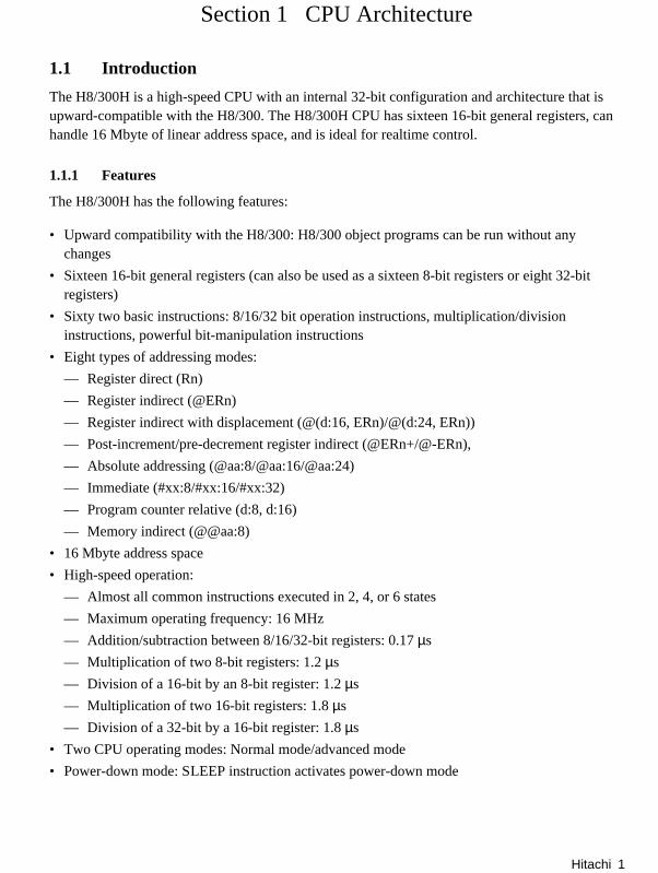
1.1 Introduction
The H8/300H is a high-speed CPU with an internal 32-bit configuration and architecture that isupward-compatible with the H8/300. The H8/300H CPU has sixteen 16-bit general registers, canhandle 16 Mbyte of linear address space, and is ideal for realtime control.
1.1.1 Features
The H8/300H has the following features:
• Upward compatibility with the H8/300: H8/300 object programs can be run without anychanges
• Sixteen 16-bit general registers (can also be used as a sixteen 8-bit registers or eight 32-bitregisters)
• Sixty two basic instructions: 8/16/32 bit operation instructions, multiplication/divisioninstructions, powerful bit-manipulation instructions
• Eight types of addressing modes:
— Register direct (Rn)
— Register indirect (@ERn)
— Register indirect with displacement (@(d:16, ERn)/@(d:24, ERn))
— Post-increment/pre-decrement register indirect (@ERn+/@-ERn),
— Absolute addressing (@aa:8/@aa:16/@aa:24)
— Immediate (#xx:8/#xx:16/#xx:32)
— Program counter relative (d:8, d:16)
— Memory indirect (@@aa:8)
• 16 Mbyte address space
• High-speed operation:
— Almost all common instructions executed in 2, 4, or 6 states
— Maximum operating frequency: 16 MHz
— Addition/subtraction between 8/16/32-bit registers: 0.17 µs
— Multiplication of two 8-bit registers: 1.2 µs
— Division of a 16-bit by an 8-bit register: 1.2 µs
— Multiplication of two 16-bit registers: 1.8 µs
— Division of a 32-bit by a 16-bit register: 1.8 µs
• Two CPU operating modes: Normal mode/advanced mode
• Power-down mode: SLEEP instruction activates power-down mode

2 Hitachi
1.1.2 Register Configuration
Figure 1.1 shows the register configuration for the H8/300H. The H8/300H CPU is composed ofsixteen 8-bit general register (R0H/R0L–R7H/R7L), eight 16-bit extended registers (E0–E7), one24-bit program counter (PC) and one 8-bit condition code register (CCR), which are used ascontrol registers.
23 0PC
015 0E0 R0H R0LE1 R1H R1LE2 R2H R2LE3 R3H R3LE4 R4H R4LE5 R5H R5LE6 R6H R6LE7 R7H R7L(SP)
Program counter
Condition code register
Stack pointer
Extension registers
I7 6 5 4 3 2 1 0
CCR
Carry flag
Overflow flag
Zero flag
Negative flag
User bit
Half-carry flag
User bit
Interrupt mask bit
Controlregisters
General registers
7 0 7
U H U N Z V C
Figure 1.1 Composition of Registers
Extended Registers: There are two ways of using extended registers:
• When working with 32-bit data and addresses (24 bits), 16-bit general registers (R0–R7) arecombined as shown in table 1.1 and used as the upper 16 bits of 32-bit registers (ERn).
• They can also be used as independent 16-bit registers (En).
Note: The function of E7 as the upper 16 bits of the stack pointer (SP) is already allocated and isused implicitly in exception processing and subroutine calls.
Hitachi 3
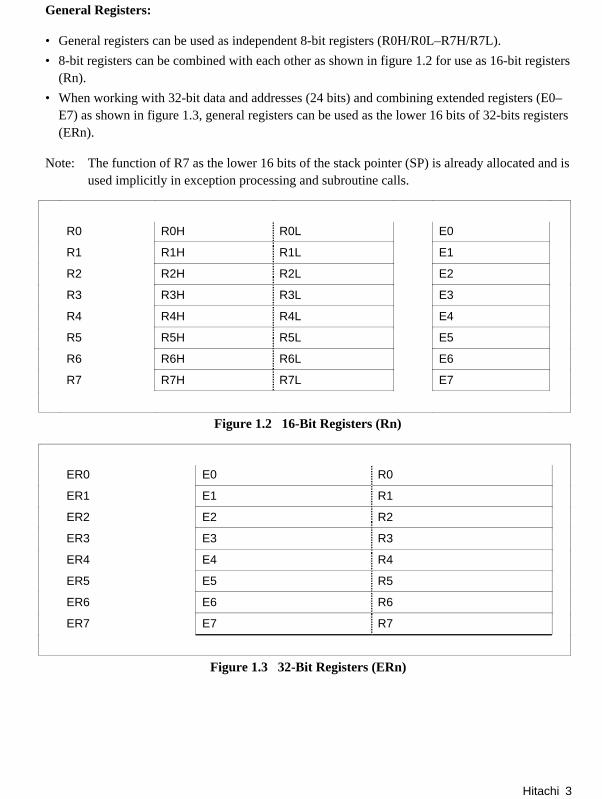
General Registers:
• General registers can be used as independent 8-bit registers (R0H/R0L–R7H/R7L).
• 8-bit registers can be combined with each other as shown in figure 1.2 for use as 16-bit registers(Rn).
• When working with 32-bit data and addresses (24 bits) and combining extended registers (E0–E7) as shown in figure 1.3, general registers can be used as the lower 16 bits of 32-bits registers(ERn).
Note: The function of R7 as the lower 16 bits of the stack pointer (SP) is already allocated and isused implicitly in exception processing and subroutine calls.
R0 R0H R0L E0
R1 R1H R1L E1
R2 R2H R2L E2
R3 R3H R3L E3
R4 R4H R4L E4
R5 R5H R5L E5
R6 R6H R6L E6
R7 R7H R7L E7
Figure 1.2 16-Bit Registers (Rn)
ER0 E0 R0
ER1 E1 R1
ER2 E2 R2
ER3 E3 R3
ER4 E4 R4
ER5 E5 R5
ER6 E6 R6
ER7 E7 R7
Figure 1.3 32-Bit Registers (ERn)
4 Hitachi
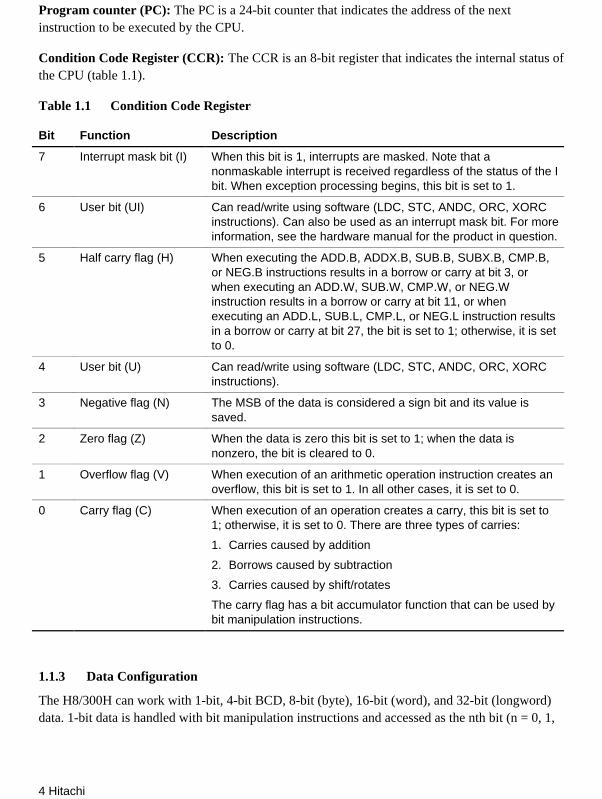
Program counter (PC): The PC is a 24-bit counter that indicates the address of the nextinstruction to be executed by the CPU.
Condition Code Register (CCR): The CCR is an 8-bit register that indicates the internal status ofthe CPU (table 1.1).
Table 1.1 Condition Code Register
Bit Function Description
7 Interrupt mask bit (I) When this bit is 1, interrupts are masked. Note that anonmaskable interrupt is received regardless of the status of the Ibit. When exception processing begins, this bit is set to 1.
6 User bit (UI) Can read/write using software (LDC, STC, ANDC, ORC, XORCinstructions). Can also be used as an interrupt mask bit. For moreinformation, see the hardware manual for the product in question.
5 Half carry flag (H) When executing the ADD.B, ADDX.B, SUB.B, SUBX.B, CMP.B,or NEG.B instructions results in a borrow or carry at bit 3, orwhen executing an ADD.W, SUB.W, CMP.W, or NEG.Winstruction results in a borrow or carry at bit 11, or whenexecuting an ADD.L, SUB.L, CMP.L, or NEG.L instruction resultsin a borrow or carry at bit 27, the bit is set to 1; otherwise, it is setto 0.
4 User bit (U) Can read/write using software (LDC, STC, ANDC, ORC, XORCinstructions).
3 Negative flag (N) The MSB of the data is considered a sign bit and its value issaved.
2 Zero flag (Z) When the data is zero this bit is set to 1; when the data isnonzero, the bit is cleared to 0.
1 Overflow flag (V) When execution of an arithmetic operation instruction creates anoverflow, this bit is set to 1. In all other cases, it is set to 0.
0 Carry flag (C) When execution of an operation creates a carry, this bit is set to1; otherwise, it is set to 0. There are three types of carries:
1. Carries caused by addition
2. Borrows caused by subtraction
3. Carries caused by shift/rotates
The carry flag has a bit accumulator function that can be used bybit manipulation instructions.
1.1.3 Data Configuration
The H8/300H can work with 1-bit, 4-bit BCD, 8-bit (byte), 16-bit (word), and 32-bit (longword)data. 1-bit data is handled with bit manipulation instructions and accessed as the nth bit (n = 0, 1,
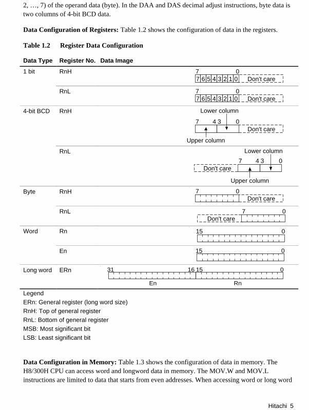
Hitachi 5
2, …, 7) of the operand data (byte). In the DAA and DAS decimal adjust instructions, byte data istwo columns of 4-bit BCD data.
Data Configuration of Registers: Table 1.2 shows the configuration of data in the registers.
Table 1.2 Register Data Configuration
Data Type Register No. Data Image
1 bit RnH
7 6 5 4 3 2 1 0 Don't care07
RnL
7 6 5 4 3 2 1 0 Don't care07
4-bit BCD RnH
Don't care07 4 3
Upper column
Lower column
RnL
Upper column
Don't care07 4 3
Lower column
Byte RnH
Don't care07
RnL
Don't care07
Word Rn
015
En
015
Long word ERn
1631 015
RnEn
LegendERn: General register (long word size)RnH: Top of general registerRnL: Bottom of general registerMSB: Most significant bitLSB: Least significant bit
Data Configuration in Memory: Table 1.3 shows the configuration of data in memory. TheH8/300H CPU can access word and longword data in memory. The MOV.W and MOV.Linstructions are limited to data that starts from even addresses. When accessing word or long word
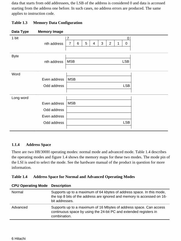
6 Hitachi
data that starts from odd addressees, the LSB of the address is considered 0 and data is accessedstarting from the address one before. In such cases, no address errors are produced. The sameapplies to instruction code.
Table 1.3 Memory Data Configuration
Data Type Memory Image
1 bit
7 6 5 4 3 2 1 07 0
nth address
Byte
MSB LSBnth address
Word
MSB
LSB
Even address
Odd address
Long word
MSB
LSB
Even address
Odd address
Even address
Odd address
1.1.4 Address Space
There are two H8/300H operating modes: normal mode and advanced mode. Table 1.4 describesthe operating modes and figure 1.4 shows the memory maps for these two modes. The mode pin ofthe LSI is used to select the mode. See the hardware manual of the product in question for moreinformation.
Table 1.4 Address Space for Normal and Advanced Operating Modes
CPU Operating Mode Description
Normal Supports up to a maximum of 64 kbytes of address space. In this mode,the top 8 bits of the address are ignored and memory is accessed on 16-bit addresses.
Advanced Supports up to a maximum of 16 Mbytes of address space. Can accesscontinuous space by using the 24-bit PC and extended registers incombination.

Hitachi 7
H'0000
H'FFFF
On-chip ROM
On-chip RAM
I/O space
Normal modeH'000000
H'FFFFFF
On-chip ROM
On-chip RAM
I/O space
Advanced mode
Figure 1.4 Memory Map
1.1.5 Addressing Mode
The H8/300H supports the eight addressing modes shown in table 1.5. The usable addressingmodes vary for each instruction. Addressing modes are explained below using the various MOVcommands as the primary example.

8 Hitachi
Table 1.5 Addressing Modes
Addressing Mode Use
Register direct Specify registers
Absolute addressing Specify address
Register indirect
Post-increment register indirect
Pre-decrement register indirect
Register indirect with displacement
Memory indirect
Program counter relative
Immediate Specify constants
Register Direct: The register name (ER0–ER7, R0–R7, E0–E7, R0H/R0L–R7H/R7L) is writtenin the operand and the contents of that register become the subject of the instruction (figure 1.5).
0 1 2 3 4 5 6 7ER0
0 1 2 3 4 5 6 7ER1
Transfer
Example: MOV.L ER0, ER1
Specifyregister
Figure 1.5 Register Direct
Absolute Addressing: Specifies the address directly. Addresses are usually specified as 24 bits inadvanced mode and 16 bits in normal mode, but can be accessed by specifying only the lowest 16bits or 8 bits when the absolute address area is 16 bits (H'000000–H'007FFF, H'FF8000–H'FFFFFF) or 8 bits (H'FFFF00–H'FFFFFF) (figure 1.6).
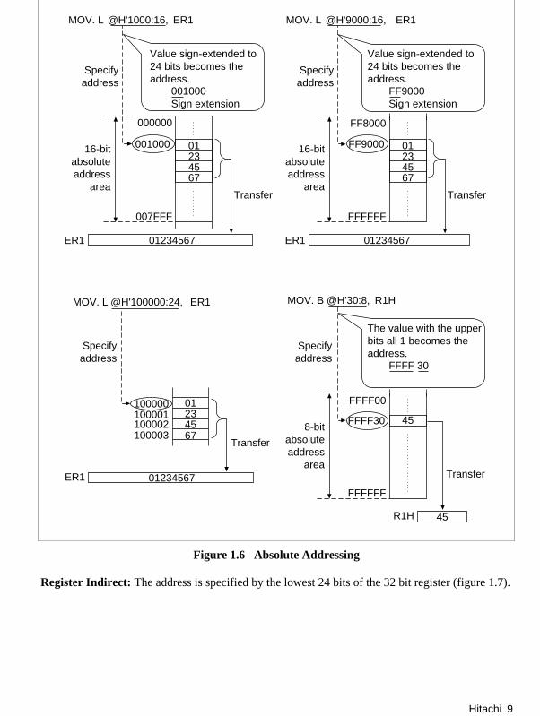
Hitachi 9
01234567
000000
007FFF
001000
01234567ER1
@H'1000:16, ER1MOV. L
Specifyaddress
16-bitabsoluteaddress
areaTransfer
01234567
FF8000
FFFFFF
FF9000
01234567ER1
@H'9000:16, ER1MOV. L
45
FFFF00
FFFFFF
FFFF30
45R1H
@H'30:8, R1HMOV. B
Value sign-extended to24 bits becomes theaddress.
01234567
100000
01234567ER1
@H'100000:24, ER1MOV. L
100002100003
001000Sign extension
Specifyaddress
16-bitabsoluteaddress
areaTransfer
Value sign-extended to24 bits becomes theaddress.
FF9000Sign extension
Specifyaddress
Specifyaddress
Transfer
Transfer
8-bitabsoluteaddress
area
The value with the upper bits all 1 becomes theaddress.
FFFF 30
100001
Figure 1.6 Absolute Addressing
Register Indirect: The address is specified by the lowest 24 bits of the 32 bit register (figure 1.7).

10 Hitachi
0 12 34 56 7
100001100000
@ER0, ER1Example: MOV. L
100002100003
Specifyaddress
100000ER0 Don't care31 24 23 0
AddressAddress specified by the lowest 24 bits of ER0
Figure 1.7 Register Indirect
Post-Increment Register Indirect: The address is specified by the lowest 24 bits of the 32 bitregister ERn. After instruction execution, the operand size value (B: 1, W: 2, L: 4) is added to thecontents of the 32-bit register ERn (figure 1.8).
0 12 34 56 7
100001100000
@ER0+, ER1Example: MOV. L
100002100003
ER0 Don't care31 24 23 0
Address
After address is specified by the lowest 24 bits of ER0, ER0 is incremented by four.
ER0 Don't care31 24 23 0
Specifiyaddress
After instructionexecution
100000
100004
Figure 1.8 Post-Increment Register Indirect

Hitachi 11
Pre-Decrement Register Indirect: The address is specified by the lowest 24 bits of the 32 bitregister ERn. Before instruction execution, the operand size value (B: 1, W: 2, L: 4) is subtractedfrom the contents of the 32-bit register ERn (figure 1.9).
0 12 34 56 7
100005100004
@–ER0, ER1Example: MOV. L
100006100007
100008ER0 Don't care31 24 23 0
Address
After ER0 is decremented by four, the address is specified by the lowest 24 bits of ER0.
100004ER0 Don't care31 24 23 0
Specifyaddress
ER0 is decrementedby four.
Figure 1.9 Pre-Decrement Register Indirect
Register Indirect with Displacement: The address is specified by the lowest 24 bits of the 32 bitregister ERn plus a signed displacement of 16 bits or 24 bits. The results of this addition are notsaved in the 32-bit register ERn (figure 1.10).

12 Hitachi
0 12 34 56 7
101001101000
@(H'1000:16. ER0), ER1Example: MOV. L
101002101003
100000ER0 Don't care31 24 23 0
(+1000)
Specifyaddress
01234567ER1
Transfer
031
101000
+)
The address is the lowest 24 bits of ER0plus the signed 16-bit displacement (+1000).
Displacement
Address
Mnemonic:@(displacement:16, ERn): signed displacement is 16 bits@(displacement:24, ERn): signed displacement is 24 bits
Figure 1.10 Register Indirect with Displacement
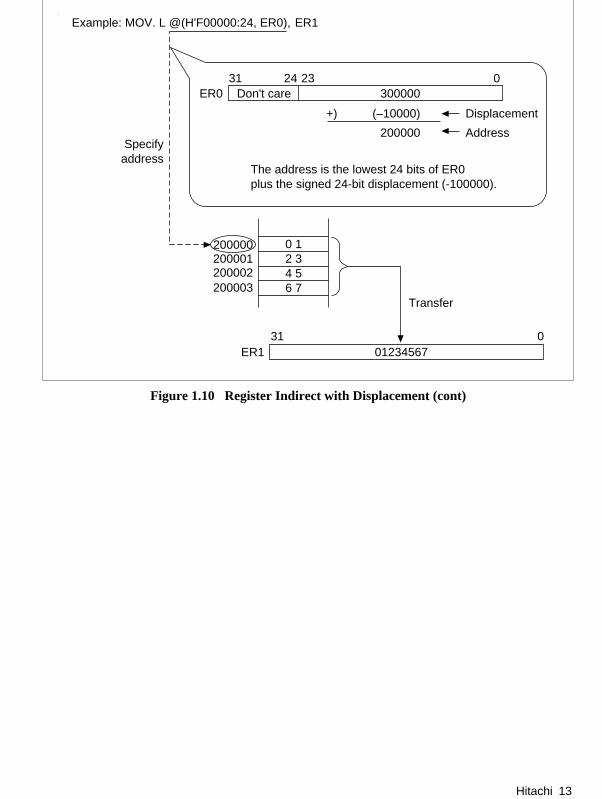
Hitachi 13
0 12 34 56 7
200001200000
@(H'F00000:24, ER0), ER1Example: MOV. L
200002200003
300000ER0 Don't care31 24 23 0
(–10000)
Specifyaddress
01234567ER1
Transfer
031
200000
+)
The address is the lowest 24 bits of ER0plus the signed 24-bit displacement (-100000).
Displacement
Address
Figure 1.10 Register Indirect with Displacement (cont)
14 Hitachi
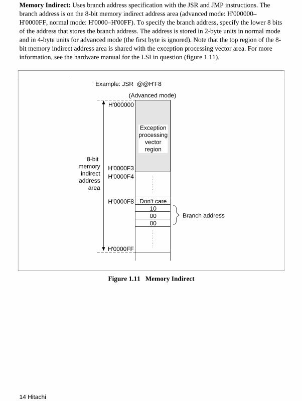
Memory Indirect: Uses branch address specification with the JSR and JMP instructions. Thebranch address is on the 8-bit memory indirect address area (advanced mode: H'000000–H'0000FF, normal mode: H'0000–H'00FF). To specify the branch address, specify the lower 8 bitsof the address that stores the branch address. The address is stored in 2-byte units in normal modeand in 4-byte units for advanced mode (the first byte is ignored). Note that the top region of the 8-bit memory indirect address area is shared with the exception processing vector area. For moreinformation, see the hardware manual for the LSI in question (figure 1.11).
H'000000
H'0000FF
(Advanced mode)
H'0000F3H'0000F4
H'0000F8
8-bit memoryindirect
addressarea
000010
Don't care
Branch address
Exceptionprocessing
vectorregion
Example: JSR @@H'F8
Figure 1.11 Memory Indirect

Hitachi 15
H'0000
H'00FF
(Normal mode)
H'0079H'007A
H'00BA
8-bitmemoryindirect
addressarea
0010
Branch address
Exceptionprocessing
vectorregion
Example: JSR @@H'BA (subroutine branch to address 1000)
Figure 1.11 Memory Indirect (cont)
Program Counter Relative: Used to specify branch addresses using the Bcc or BSR instructions.It specifies the displacement of the branch address (signed 8-bit or signed 16-bit). Displacement isadded to the contents of the PC and the address at the branch destination is generated. The PCcontents become the start address of the next instruction, so the branchable area for the Bcc andBSR instructions are –126 to +128 bytes or –32766 to +32678 bytes. Normally, the branchdestination symbol is specified rather than the displacement (figure 1.12).
BSR
ADD. W
ABC
R0, E1ABC:
Figure 1.12 Program Counter Relative
16 Hitachi
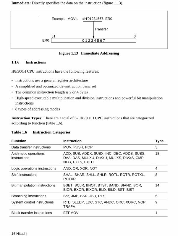
Immediate: Directly specifies the data on the instruction (figure 1.13).
0 1 2 3 4 5 6 7ER0
Transfer
Example: MOV.L #H'01234567, ER0
31 0
Figure 1.13 Immediate Addressing
1.1.6 Instructions
H8/300H CPU instructions have the following features:
• Instructions use a general register architecture
• A simplified and optimized 62-instruction basic set
• The common instruction length is 2 or 4 bytes
• High-speed executable multiplication and division instructions and powerful bit manipulationinstructions
• 8 types of addressing modes
Instruction Types: There are a total of 62 H8/300H CPU instructions that are categorizedaccording to function (table 1.6).
Table 1.6 Instruction Categories
Function Instruction Type
Data transfer instructions MOV, PUSH, POP 3
Arithmetic operationsinstructions
ADD, SUB, ADDX, SUBX, INC, DEC, ADDS, SUBS,DAA, DAS, MULXU, DIVXU, MULXS, DIVXS, CMP,NEG, EXTS, EXTU
18
Logic operations instructions AND, OR, XOR, NOT 4
Shift instructions SHAL, SHAR, SHLL, SHLR, ROTL, ROTR, ROTXL,ROTXR
8
Bit manipulation instructions BSET, BCLR, BNOT, BTST, BAND, BIAND, BOR,BIOR, BXOR, BIXOR, BLD, BILD, BST, BIST
14
Branching instructions Bcc, JMP, BSR, JSR, RTS 5
System control instructions RTE, SLEEP, LDC, STC, ANDC, ORC, XORC, NOP,TRAPA
9
Block transfer instructions EEPMOV 1

Hitachi 17
Section 2 Instructions
2.1 Data Transfer Instructions
2.1.1 MOV
MOV (Move): Transfers 8-bit, 16-bit or 32-bit data (figure 2.1).
BWL
MOV.
Destination operandSource operandOperand sizeMnemonic
,
Figure 2.1 MOV

18 Hitachi
Table 2.1 MOV
Mnem-onic
Op.Sz.
SourceOperand
Dest.Op. Description
MOV B RnH or RnL RnH orRnL
7 0 7 0
RnH or RnL RnH or RnL
W Rn or En Rn orEn
15 0 15 0
L ERn ERn
31 0 31 0
ERn ERn
B @ERn@(d:16,ERn)@(d:24,ERn)@–ERn
RnH orRnL
7 0
RnH or RnL
W @aa:8@aa:16@aa:24
Rn orEn
15 0Rn or EnEven address
L ERn
31 0ERn
Even address
B RnH or RnL @ERn@(d:16,ERn)
7 0
RnH or RnL
W Rn or En@(d:24,ERn)@ERn+@aa:8@aa:16
15 0Rn or En
Even address
L ERn
@aa:24
31 0ERn
Even address
Hitachi 19
Table 2.1 MOV (cont)
Mnem-onic
Op.Size
SourceOperand
Dest.Op. Description
MOV(cont)
B #xx:8 RnHorRnL
7 0#xx:8
RnH or RnL
W #xx:16 Rn orEn
15 0#xx:16
Rn or En
L #xx:32 ERn
31 0#xx:32
ERn
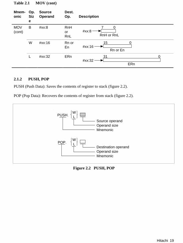
2.1.2 PUSH, POP
PUSH (Push Data): Saves the contents of register to stack (figure 2.2).
POP (Pop Data): Recovers the contents of register from stack (figure 2.2).
PUSH.WL
POP.
Source operandOperand sizeMnemonic
Destination operandOperand sizeMnemonic
WL
Figure 2.2 PUSH, POP

20 Hitachi
Table 2.2 PUSH, POP
Mnem-onic
SourceOperand
DestinationOperand(SourceOperand) Description
PUSH W (Rn, En) After 2 is subtracted from the stack pointer, the contents of16-bit registers Rn and En are saved to the stack.
Stack
H'×× ××En or Rn
SP
SP–2
15 0
The instruction is the same as MOV.W Rn, @–SP or MOV.WEn, @–SP.
L (ERn) After 4 is subtracted from the stack pointer, the contents of32-bit register ERn are saved to the stack.
H'×× ×× ×× ××
Stack
ERn
SP
SP
–431 0
The instruction is the same as MOV.L ERn, @SP–.
POP W Rn, En The contents of 16-bit registers Rn and En saved to the stackare recovered. After recovery 2 is added to the stack pointer.
H'××××15 0
Stack
En or Rn
SP
SP+2
The instruction is the same as MOV.W @SP+,Rn or MOV.W@SO+, En.
L ERn The contents of 32-bit register ERn saved to the stack arerecovered. After recovery 4 is added to the stack pointer.
StackH'××
××
31 0
ERn
SP
SP
××××
+4
The instruction is the same as MOV.> @SP+, ERn.
Hitachi 21
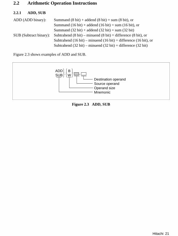
2.2 Arithmetic Operation Instructions
2.2.1 ADD, SUB
ADD (ADD binary): Summand (8 bit) + addend (8 bit) = sum (8 bit), orSummand (16 bit) + addend (16 bit) = sum (16 bit), orSummand (32 bit) + addend (32 bit) = sum (32 bit)
SUB (Subtract binary): Subtrahend (8 bit) – minuend (8 bit) = difference (8 bit), orSubtrahend (16 bit) – minuend (16 bit) = difference (16 bit), orSubtrahend (32 bit) – minuend (32 bit) = difference (32 bit)
Figure 2.3 shows examples of ADD and SUB.
ADDSUB
BW
Destination operandSource operandOperand sizeMnemonic
. ,
Figure 2.3 ADD, SUB

22 Hitachi
Table 2.3 ADD, SUB
Mnem-onic
OperandSize
DestinationOperand
SourceOperand Description
ADDSUB
B RmH or RmL #xx:8or RnHor RnL
7 07 0
RmH or RmL
RnH or RnL
=±H'××H'××
H'××#xx:8
W Rm or Em #xx:16or Rn orEn
H'×××× ± =H'××××#xx:16
Rn or EnH'××××Rm or Em
L ERm #xx:32 orERn
H'××××××××H'××××××××
H'××××××××#xx:32± =
ERnERm
2.2.2 ADDX, SUBX
ADDX (ADD with Extend Carry): Adds with C flag (carry from bottom) included (figure 2.4).
SUBX (Subtract with Extend Carry): Subtracts with C flag (borrow from bottom) included (figure2.4).
ADDXSUBX . B
Destination operandSource operandMnemonic
,
Figure 2.4 ADDX, SUBX

Hitachi 23
Table 2.4 ADDX, SUBX
Mnem-onic
OperandSize
SourceOperand
DestinationOperand Description
ADDXSUBX
B #xx:8 orRnH or RnL
RmH orRmL
7 0H'××#xx:8
H'××H'××
RmH or RmLRnH or RnL
C flag± =±
2.2.3 INC, DEC
INC (Increment): Adds 1 to contents of 8-bit, registers RnH or RnL (figure 2.5). Adds 2 to thecontents of 16-bit registers Rn or En and 32-bit register ERn.
DEC (DECrement): Subtracts 1 from contents of 8-bit, registers RnH or RnL (figure 2.5).Subtracts 2 from the contents of 16-bit registers Rn or En and 32-bit register ERn.
INCDEC
INCDEC
WL
B
#1#2
Destination operandOperand sizeMnemonic
Destination operandOperand sizeMnemonic
. ,
.
Figure 2.5 INC, DEC

24 Hitachi
Table 2.5 INC, DEC
Mnem-onic
OperandSize
DestinationOperand Description
INCDEC
B RnH or RnL
7 0H'××
RnH or RnL±1 =
W Rn or En
H'××××Rn or En
±12 =
15 0
L ERn
H'××××××××ERn
31 0±
12 =
2.2.4 ADDS, SUBS
ADDS (Add with Sign Extension): Adds 1, 2 or, 4 to the contents of the 32-bit register ERn(figure 2.6).
SUBS (Subtract with Sign Extension): Subtracts 1, 2 or 4, from the contents of the 32-bit registerERn (figure 2.6).
ADDSSUBS
#1#2#4
ERn
Destination operandSource operandMnemonic
,
Figure 2.6 ADDS, SUBS
Table 2.6 ADDS, SUBS
Mnem-onic
OperandSize
SourceOperand
DestinationOperand Description
ADDSSUBS
— #1 or #2or #4
ERn
31 0H'××××××××
124
=±ERn
Hitachi 25
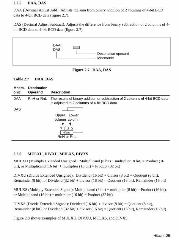
2.2.5 DAA, DAS
DAA (Decimal Adjust Add): Adjusts the sum from binary addition of 2 columns of 4-bit BCDdata to 4-bit BCD data (figure 2.7).
DAS (Decimal Adjust Subtract): Adjusts the difference from binary subtraction of 2 columns of 4-bit BCD data to 4-bit BCD data (figure 2.7).
DAADAS
Destination operandMnemonic
Figure 2.7 DAA, DAS
Table 2.7 DAA, DAS
Mnem-onic
DestinationOperand Description
DAA RnH or RnL The results of binary addition or subtraction of 2 columns of 4-bit BCD datais adjusted to 2 columns of 4-bit BCD data.
DAS
Uppercolumn
7 04 3H'××
RnH or RnL
Lowercolumn
2.2.6 MULXU, DIVXU, MULXS, DIVXS
MULXU (Multiply Extended Unsigned): Multiplicand (8 bit) + multiplier (8 bit) = Product (16bit), or Multiplicand (16 bit) + multiplier (16 bit) = Product (32 bit)
DIVXU (Divide Extended Unsigned): Dividend (16 bit) + divisor (8 bit) = Quotient (8 bit),Remainder (8 bit), or Dividend (32 bit) + divisor (16 bit) = Quotient (16 bit), Remainder (16 bit)
MULXS (Multiply Extended Signed): Multiplicand (8 bit) + multiplier (8 bit) = Product (16 bit),or Multiplicand (16 bit) + multiplier (16 bit) = Product (32 bit)
DIVXS (Divide Extended Signed): Dividend (16 bit) + divisor (8 bit) = Quotient (8 bit),Remainder (8 bit), or Dividend (32 bit) + divisor (16 bit) = Quotient (16 bit), Remainder (16 bit)
Figure 2.8 shows examples of MULXU, DIVXU, MULXS, and DIVXS.
26 Hitachi
MULXUMULXSDIVXUDIVXS
. BW ,
Destination operandSource operandOperand sizeMnemonic
Figure 2.8 MULXU, DIVXU, MULXS, DIVXS
Table 2.8 MULXU, DIVXU, MULXS, DIVXS
Mnem-onic
Op.Size
SourceOperand
DestinationOperand Description
MULXUMULXS
B RnH orRnL
Rm or Em
ProductH'××××
15 0
Rm or Em=H'×× ×
87 7 0
RnH or RnLH'××
W Rn or En ERm
ERm
31 16 15 0 × =
15 0
Rn or EnH'×××× H'××××
ProductH'××××××××
DIVXUDIVXS
B RnH orRnL
Rm or Em
RemainderH'××
QuotientH'××
7 015 0÷ =
Rm or Em RnH or RnL
8 7H'×××× H'××
W Rn or En ERm
QuotientH'××××
RemainderH'××××
H'×××××××× H'××××ERm Rn or En
÷ =31 16 15 0 15 0

Hitachi 27
2.2.7 CMP
CMP (Compare): Compares pairs of 8-bit, 16-bit, or 32-bit data (figure 2.9).
CMP .BWL
Destination operandSource operandOperand sizeMnemonic
,
Figure 2.9 CMP
Table 2.9 CMP
Mnem-onic
Op.Size
SourceOp.
Dest.Op. Description
CMP B #xx:8RnH orRnL
RnHorRnL
H' × ×H'××
7 0–
H'××#xx:87 0
RnH or RnLRnH or RnL
W #xx:16or Rnor En
Rn orEn
H'××××H'××××
H'××××#xx:16
–
Rn or EnRn or En
15 015 0
L #xx:32or ERn
ERn
H'××××××××31 0
H'××××××××
H'××××××××#xx:32
ERn
ERn
–31 0
28 Hitachi
2.2.8 NEG
NEG (Negate): Takes the two complement of 8-bit registers RnH and RnL, 16-bit registers Rn andEn, and 32-bit register ERn. (figure 2.10)
NEGBWL
.
Destination operandOperand sizeMnemonic
Figure 2.10 NEG
Table 2.10 NEG
Mnem-onic
Op.Size
DestinationOperand Description
NEG B RnH or RnL
H'××RnH or RnL
0 –7 0
=
W Rn or En
H'××××0 –015
Rn or En
=
L ERn
H'××××××××0 –31
ERn
=0
2.2.9 EXTS, EXTU
EXTS (Extend as Signed): Sign-extends from 8 bit to 16 bit or from 16 bit to 32 bit (figure 2.11).
EXTU (Extend as Unsigned): Zero-extends from 8 bit to 16 bit or from 16 bit to 32 bit (figure2.11).
EXTSEXTU W
L.
Destination operandOperand sizeMnemonic
Figure 2.11 EXTS, EXTU
Hitachi 29
Table 2.11 EXTS, EXTU
Mnem-onic
Op.Size
DestinationOperand Description
EXTU W Rn or En
Rn or En
Zero extended
15 8 7H' × ×H' 00
0
L ERn
0H' × × × ×H' 0000
Zero extended
31 16 15
ERn
EXTS W Rn or En
H'××H' 00Rn or En
Sign extended
15 8 7 0
H'××H' FFRn or En
15 8 7 0
Sign extension
When positive
When negative
L ERn
H'××××H' 0000
H' FFFF H'××××
Sign extended
031 16 15
031 16 15
Sign extension
When positive
When negativeERn
ERn
30 Hitachi
2.3 Logic Operation Instructions
2.3.1 AND, OR, XOR, NOT
AND (And logical): Takes the logical product of pairs of 8-bit, 16-bit, or 32-bit data (figure 2.12).
OR (Inclusive Or Logical): Takes the logical sum pairs of 8-bit, 16-bit, or 32-bit data (figure 2.12).
XOR (Exclusive Or Logical): Takes the exclusive logical sum of pairs of 8-bit, 16-bit, or 32-bitdata (figure 2.12).
NOT (NOT = Logical Complement): Logically inverts pairs of 8-bit, 16-bit, or 32-bit data(figure2.12).
ANDORXOR
NOT.
BWL
BWL
. ,
Destination operandSource operandOperand sizeMnemonic
Destination operandOperand sizeMnemonic
Figure 2.12 AND, OR, XOR, NOT
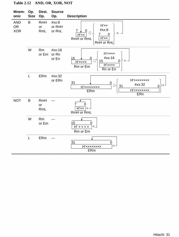
Hitachi 31
Table 2.12 AND, OR, XOR, NOT
Mnem-onic
Op.Size
Dest.Op.
SourceOp. Description
ANDORXOR
B RmHorRmL
#xx:8or RnHor RnL
7 0=∧H'××
H'××
H'××#xx:8
7 0RmH or RmL
RnH or RnL
W Rmor Em
#xx:16or Rnor En
H'××××#xx:1615
15 0 =∧
Rm or EmRn or En
H'××××H'××××
0
L ERm #xx:32or ERn
31 0H'××××××××
H'××××××××31 0
H'××××××××#xx:32 =∧
ERmERn
NOT B RmHorRmL
—
7 0H'××
RmH or RmL=
W Rmor Em
—
H' × × × ×15
Rm or Em
0=
L ERm —
31H'××××××××
ERm
0=
32 Hitachi
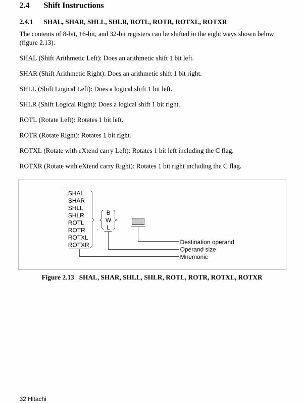
2.4 Shift Instructions
2.4.1 SHAL, SHAR, SHLL, SHLR, ROTL, ROTR, ROTXL, ROTXR
The contents of 8-bit, 16-bit, and 32-bit registers can be shifted in the eight ways shown below(figure 2.13).
SHAL (Shift Arithmetic Left): Does an arithmetic shift 1 bit left.
SHAR (Shift Arithmetic Right): Does an arithmetic shift 1 bit right.
SHLL (Shift Logical Left): Does a logical shift 1 bit left.
SHLR (Shift Logical Right): Does a logical shift 1 bit right.
ROTL (Rotate Left): Rotates 1 bit left.
ROTR (Rotate Right): Rotates 1 bit right.
ROTXL (Rotate with eXtend carry Left): Rotates 1 bit left including the C flag.
ROTXR (Rotate with eXtend carry Right): Rotates 1 bit right including the C flag.
BWL
SHALSHARSHLLSHLRROTLROTRROTXLROTXR Destination operand
Operand sizeMnemonic
.
Figure 2.13 SHAL, SHAR, SHLL, SHLR, ROTL, ROTR, ROTXL, ROTXR

Hitachi 33
Table 2.13 SHAL, SHAR, SHLL, SHLR, ROTL, ROTR, ROTXL, ROTXR
Mnem-onic
DestinationOperand Description
SHAL RnH orRnL, Rn orEn, ERn
MSB LSBC flag0
RnH or RnL, Rn or En, ERn
SHAR
MSB LSB C flag
RnH or RnL, Rn or En, ERn
SHLL
MSB LSBC flag0
RnH or RnL, Rn or En, ERn
SHLR
MSB LSB C flag
RnH or RnL, Rn or En, ERn0
ROTL
MSB LSBC flag
RnH or RnL, Rn or En, ERn
ROTR
MSB LSB C flag
RnH or RnL, Rn or En, ERn
ROTXL
MSB LSBC flag
RnH or RnL, Rn or En, ERn
ROTXR
MSB LSB C flag
RnH or RnL, Rn or En, ERn

34 Hitachi
2.5 Bit Manipulation Instructions
2.5.1 BSET, BCLR, BNOT, BTST, BLD, BILD, BST, BIST, BAND, BIAND, BOR, BIOR,BXOR, BIXOR
Bit data can be accessed in the format of the nth bit (n = 0, 1, 2, …, 7) of the 8-bit data in the 8-bitregisters (R0H–R7H, R0L–R7L) or on memory. The bit numbers for such accesses are specifiedas 3-bit immediate data or 8-bit register contents (lower 3 bits) (figure 2.14).
BSETBCLRBNOTBTSTBLDBILDBSTBISTBANDBIANDBORBIORBXORBIXOR
#0#1#2#3#4#5#6#7
. B
7 6 5 4 3 2 1 0
8-bit register(R0H–R7H, R0L–R7L)
7 6 5 4 3 2 1 0
Memory(register indirect,
8-bit absolute address)
or
8-bit data
8-bit register (lower 3 bits)(R0H–R7H, R0L–R7L)
000–111
or Immediate data#0–#7
Bit numbers (0–7)
,
Figure 2.14 BSET, BCLR, BNOT, BTST, BLD, BILD, BST, BIST, BAND, BIAND, BOR,BIOR, BXOR, BIXOR
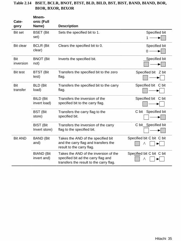
Hitachi 35
Table 2.14 BSET, BCLR, BNOT, BTST, BLD, BILD, BST, BIST, BAND, BIAND, BOR,BIOR, BXOR, BIXOR
Cate-gory
Mnem-onic (FullName) Description
Bit set BSET (Bitset)
Sets the specified bit to 1.
1
Specified bit
Bit clear BCLR (Bitclear)
Clears the specified bit to 0.
0
Specified bit
Bitinversion
BNOT (Bitnot)
Inverts the specified bit.
Specified bit
Bit test BTST (Bittest)
Transfers the specified bit to the zeroflag.
Specified bit Z bit
Bittransfer
BLD (Bitload)
Transfers the specified bit to the carryflag.
Specified bit C bit
BILD (Bitinvert load)
Transfers the inversion of thespecified bit to the carry flag.
Specified bit C bit
BST (Bitstore)
Transfers the carry flag to thespecified bit.
Specified bitC bit
BIST (BitInvert store)
Transfers the inversion of the carryflag to the specified bit.
Specified bitC bit
Bit AND BAND (Bitand)
Takes the AND of the specified bitand the carry flag and transfers theresult to the carry flag.
Specified bit C bit C bit
BIAND (Bitinvert and)
Takes the AND of the inversion of thespecified bit ad the carry flag andtransfers the result to the carry flag.
Specified bit C bit C bit

36 Hitachi
Table 2.14 BSET, BCLR, BNOT, BTST, BLD, BILD, BST, BIST, BAND, BIAND, BOR,BIOR, BXOR, BIXOR (cont)
Cate-gory
Mnem-onic (FullName) Description
Bit OR BOR (Bitinclusive or)
Takes the OR of the specified bit andthe carry flag and transfers the resultto the carry flag.
Specified bit C bit C bit
BIOR (Bitinvertinclusive or)
Takes the OR of the inversion of thespecified bit and the carry flag andtransfers the result to the carry flag.
Specified bit C bit C bit
BitexclusiveOr
BXOR (Bitexclusive or)
Takes the exclusive OR of thespecified bit and the carry flag andtransfers the result to the carry flag.
Specified bit C bit C bit
BIXOR ( Bitinvertexclusive or)
Takes the exclusive OR of theinversion of the specified bit and thecarry flag and transfers the result tothe carry flag.
Specified bit C bit C bit
2.6 Branch Instructions
2.6.1 Bcc
Bcc (Branch Conditionally): This instruction branches when a condition is met (figure 2.15).
BccOperandMnemonic
Figure 2.15 Bcc
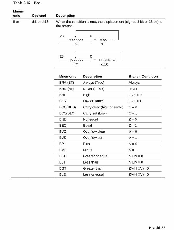
Hitachi 37
Table 2.15 Bcc
Mnem-onic Operand Description
Bcc d:8 or d:16 When the condition is met, the displacement (signed 8 bit or 16 bit) tothe branch
H'××××××
H'××××××
+ H'××d:8
+ H'××××d:16
PC
PC
=
=
23 0
23 0
Mnemonic Description Branch Condition
BRA (BT) Always (True) Always
BRN (BF) Never (False( never
BHI High CVZ = 0
BLS Low or same CVZ = 1
BCC(BHS) Carry clear (high or same) C = 0
BCS(BLO) Carry set (Low) C = 1
BNE Not equal Z = 0
BEQ Equal Z = 1
BVC Overflow clear V = 0
BVS Overflow set V = 1
BPL Plus N = 0
BMI Minus N = 1
BGE Greater or equal N ⊕ V = 0
BLT Less than N ⊕ V = 0
BGT Greater than ZV(N ⊕ V) =0
BLE Less or equal ZV(N ⊕ V) =0
38 Hitachi
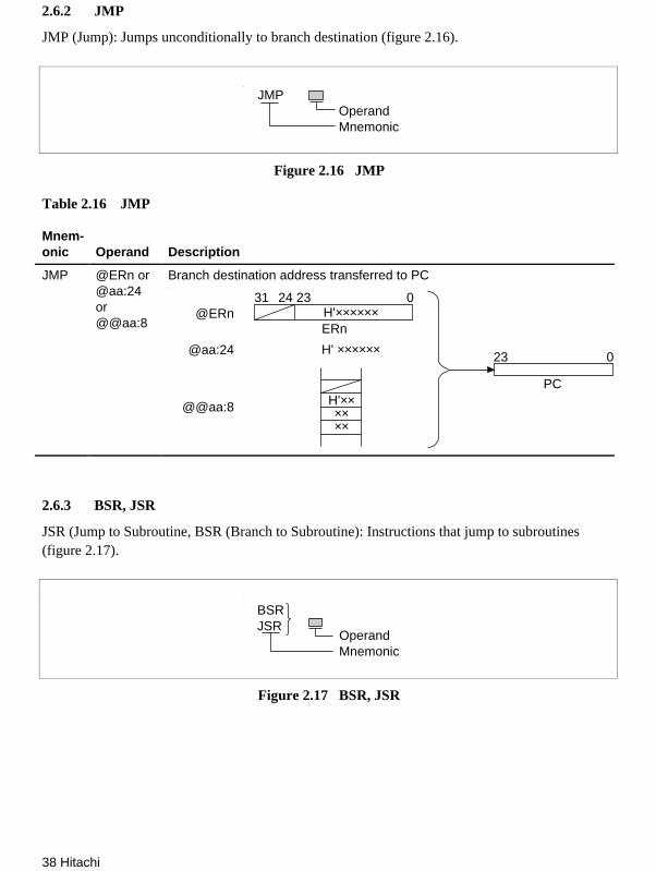
2.6.2 JMP
JMP (Jump): Jumps unconditionally to branch destination (figure 2.16).
JMPOperandMnemonic
Figure 2.16 JMP
Table 2.16 JMP
Mnem-onic Operand Description
JMP @ERn or@aa:24or@@aa:8
Branch destination address transferred to PC
H'××
@ERn
@aa:24
@@aa:8
H'××××××
H' ××××××
××××
31 24 23
023
PC
ERn
0
2.6.3 BSR, JSR
JSR (Jump to Subroutine, BSR (Branch to Subroutine): Instructions that jump to subroutines(figure 2.17).
BSRJSR
OperandMnemonic
Figure 2.17 BSR, JSR
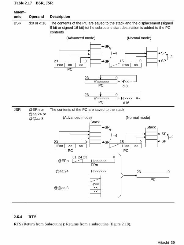
Hitachi 39
Table 2.17 BSR, JSR
Mnem-onic Operand Description
BSR d:8 or d:16 The contents of the PC are saved to the stack and the displacement (signed8 bit or signed 16 bit) tot he subroutine start destination is added to the PCcontents
H'××××××
(Advanced mode) (Normal mode)
H'×× ×× ××
SP
PC
23 0 SP
23 0
PCH'××d:8
=+
H'××××××23 0
PCH'××××
d16 +
H'××
SP
SP–2
–4
=
××15 0
JSR @ERn or@aa:24 or@@aa:8
The contents of the PC are saved to the stack
SP–2
15 0 SPH'××
(Advanced mode) (Normal mode)
×× ××PC PC
SP
SP
StackStack
23 0
–4
H'×× ××
31 24 23 0
ERn@ERn H'××××××
@aa:24 H'××××××
@@aa:8H'××
××××
23 0
PC
2.6.4 RTS
RTS (Return from Subroutine): Returns from a subroutine (figure 2.18).
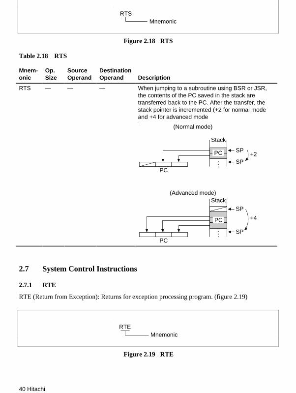
40 Hitachi
RTSMnemonic
Figure 2.18 RTS
Table 2.18 RTS
Mnem-onic
Op.Size
SourceOperand
DestinationOperand Description
RTS — — — When jumping to a subroutine using BSR or JSR,the contents of the PC saved in the stack aretransferred back to the PC. After the transfer, thestack pointer is incremented (+2 for normal modeand +4 for advanced mode
(Normal mode)
Stack
SP
SP+2
PC
PC
PC
SP
+4
SP
...
...PC
(Advanced mode)Stack
2.7 System Control Instructions
2.7.1 RTE
RTE (Return from Exception): Returns for exception processing program. (figure 2.19)
RTEMnemonic
Figure 2.19 RTE
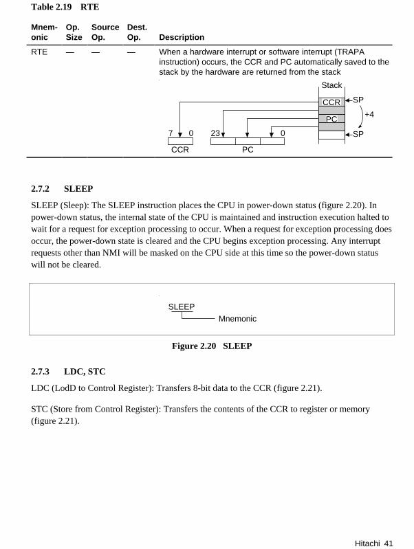
Hitachi 41
Table 2.19 RTE
Mnem-onic
Op.Size
SourceOp.
Dest.Op. Description
RTE — — — When a hardware interrupt or software interrupt (TRAPAinstruction) occurs, the CCR and PC automatically saved to thestack by the hardware are returned from the stack
Stack
SP
SP
+4
CCR PC
CCR
PC
7 0 23 0
2.7.2 SLEEP
SLEEP (Sleep): The SLEEP instruction places the CPU in power-down status (figure 2.20). Inpower-down status, the internal state of the CPU is maintained and instruction execution halted towait for a request for exception processing to occur. When a request for exception processing doesoccur, the power-down state is cleared and the CPU begins exception processing. Any interruptrequests other than NMI will be masked on the CPU side at this time so the power-down statuswill not be cleared.
SLEEPMnemonic
Figure 2.20 SLEEP
2.7.3 LDC, STC
LDC (LodD to Control Register): Transfers 8-bit data to the CCR (figure 2.21).
STC (Store from Control Register): Transfers the contents of the CCR to register or memory(figure 2.21).
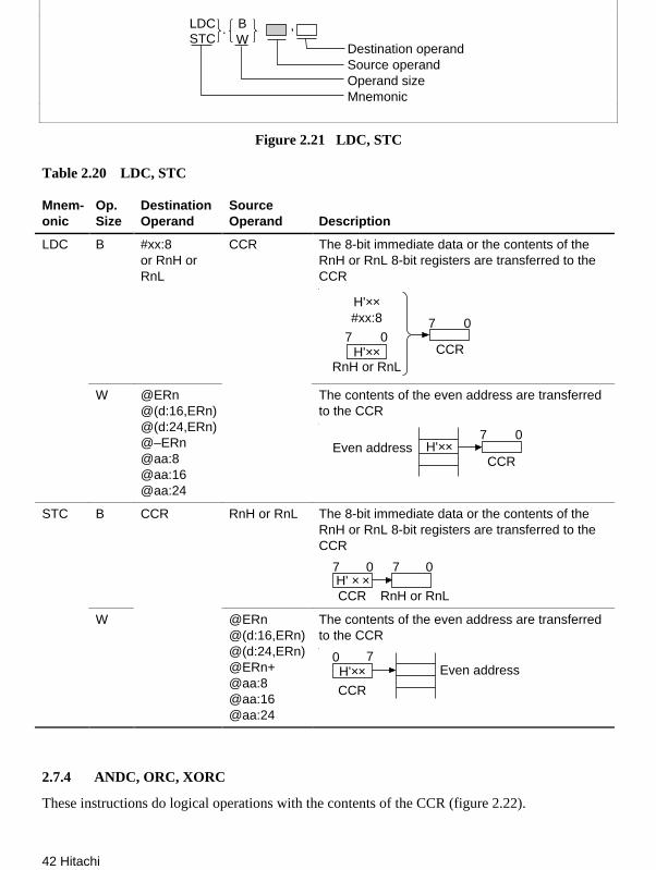
42 Hitachi
STCLDC B
W. ,
Destination operandSource operandOperand sizeMnemonic
Figure 2.21 LDC, STC
Table 2.20 LDC, STC
Mnem-onic
Op.Size
DestinationOperand
SourceOperand Description
LDC B #xx:8or RnH orRnL
CCR The 8-bit immediate data or the contents of theRnH or RnL 8-bit registers are transferred to theCCR
H'××
H'××#xx:8
7 07 0
CCRRnH or RnL
W @ERn@(d:16,ERn)@(d:24,ERn)@–ERn@aa:8@aa:16@aa:24
The contents of the even address are transferredto the CCR
H'××Even addressCCR
7 0
STC B CCR RnH or RnL The 8-bit immediate data or the contents of theRnH or RnL 8-bit registers are transferred to theCCR
CCRH' × ×
7 0 7 0
RnH or RnL
W @ERn@(d:16,ERn)@(d:24,ERn)@ERn+@aa:8@aa:16@aa:24
The contents of the even address are transferredto the CCR
H'××0 7
Even address
CCR
2.7.4 ANDC, ORC, XORC
These instructions do logical operations with the contents of the CCR (figure 2.22).
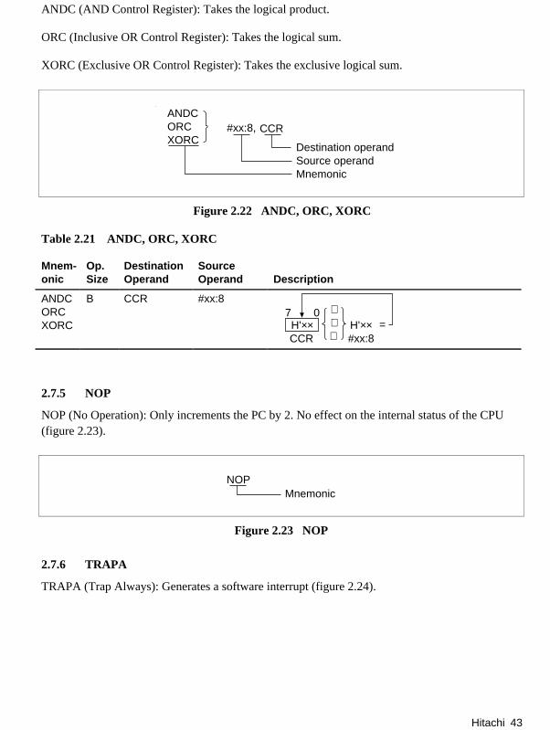
Hitachi 43
ANDC (AND Control Register): Takes the logical product.
ORC (Inclusive OR Control Register): Takes the logical sum.
XORC (Exclusive OR Control Register): Takes the exclusive logical sum.
ANDCORCXORC
#xx:8, CCR
Destination operandSource operandMnemonic
Figure 2.22 ANDC, ORC, XORC
Table 2.21 ANDC, ORC, XORC
Mnem-onic
Op.Size
DestinationOperand
SourceOperand Description
ANDCORCXORC
B CCR #xx:8
H'××7 0
CCR
∧∨⊕
H'××#xx:8
=
2.7.5 NOP
NOP (No Operation): Only increments the PC by 2. No effect on the internal status of the CPU(figure 2.23).
NOPMnemonic
Figure 2.23 NOP
2.7.6 TRAPA
TRAPA (Trap Always): Generates a software interrupt (figure 2.24).

44 Hitachi
TRAPA
#0#1#2#3
Figure 2.24 TRAPA
Table 2.22 TRAPA
Mnem-onic Operand Description
ANDCORCXORC
#0 or #1 or#2 or #3
CCR and PC saved to stack
H'×× H'×× ×× ××CCR PC
CCR1I
SP
SP
–4
Vector Address
#xx Normal Mode Advanced Mode
0 H’0008–H’0009 H’000010–H000013
1 H’000A–H’000B H’000014–H000017
2 H’000C–H’000D
H’000018–H00001B
3 H’000E–H’000F H’00001C–H00001F
2.8 Block Transfer Instructions
2.8.1 EEPMOV
EEPMOV (Move data to EEPROM): Transfer block data to any address. No interrupts will bedetected during the data transfer (figure 2.25).
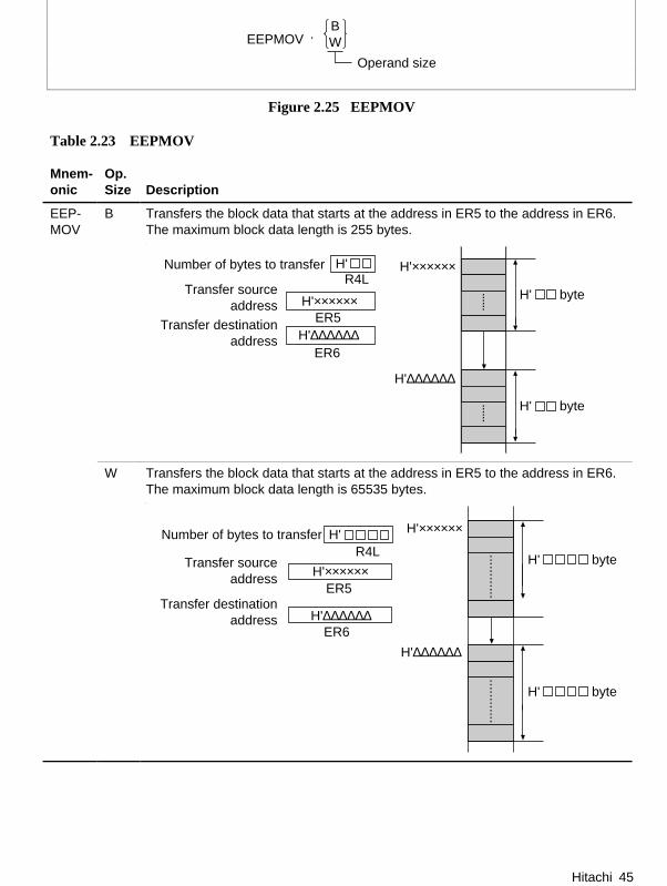
Hitachi 45
EEPMOVBW
Operand size
.
Figure 2.25 EEPMOV
Table 2.23 EEPMOV
Mnem-onic
Op.Size Description
EEP-MOV
B Transfers the block data that starts at the address in ER5 to the address in ER6.The maximum block data length is 255 bytes.
H'××××××
H'∆∆∆∆∆∆
H' H'××××××
Transfer sourceaddress
Transfer destinationaddress
R4L
ER5
ER6
Number of bytes to transfer
......
......
H'∆∆∆∆∆∆
H' byte
H' byte
W Transfers the block data that starts at the address in ER5 to the address in ER6.The maximum block data length is 65535 bytes.
Number of bytes to transfer
ER5
ER6
H'××××××
H'∆∆∆∆∆∆
R4L
H'∆∆∆∆∆∆
H'××××××
Transfer sourceaddress
Transfer destinationaddress
........
..
..
........
..
..
H' byte
H' byte
H'

46 Hitachi
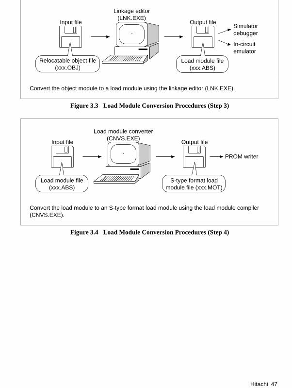
Section 3 Load Module Conversion Procedures
Figures 3.1 through 3.4 show the load module conversion procedures for the H8/300H.
Editor(e.g. MIFES)
Assembler source file(xxx.SRC)
Create the assembler source program using any editor (such as MIFES).
Figure 3.1 Load Module Conversion Procedures (Step 1)
Input file
Assembler source file(xxx.SRC)
Assembler(ASM38.EXE)
Output file
Relocatable object file(xxx.OBJ), List file (xxx.LIS)
Convert the assembler source program to an object module using the assembler (ASM38.EXE).
Figure 3.2 Load Module Conversion Procedures (Step 2)
Hitachi 47
Input file Output file
Linkage editor(LNK.EXE)
Load module file(xxx.ABS)
Relocatable object file(xxx.OBJ)
Simulatordebugger
In-circuitemulator
Convert the object module to a load module using the linkage editor (LNK.EXE).
Figure 3.3 Load Module Conversion Procedures (Step 3)
Load module converter(CNVS.EXE)
Input file Output file
Load module file(xxx.ABS)
S-type format loadmodule file (xxx.MOT)
PROM writer
Convert the load module to an S-type format load module using the load module compiler (CNVS.EXE).
Figure 3.4 Load Module Conversion Procedures (Step 4)
48 Hitachi
Section 4 Examples of Software Applications
4.1 Software Applications Examples
Table 4.1 lists software application examples.
Table 4.1 List of Software Application Examples
Software title Label Use Section
Block transfer MOVE MOV.L instruction, post-incrementregister indirect
4.3
Block transfer using block transferinstruction
EEPMOV EEPMOV.W instruction 4.4
Branching using a table CCASE Register indirect with displacement 4.5
Count of number of logical 1 bits in8-bit data
HCNT ROTL.B instruction, ADDX.Binstruction
4.6
Find first 1 in 32-bit data FIND1 SHLL.L instruction 4.7
64-bit binary addition ADD ADD.L instruction 4.8
64-bit binary subtraction SUB SUB.L instruction 4.9
Unsigned 32-bit binary multiplication MUL MULXU.W instruction 4.10
Unsigned 32-bit binary division DIV SHLL.L instruction, ROTL.Linstruction
4.11
Signed 16-bit binary multiplication MULXS MULXS.W instruction 4.12
Signed 32-bit binary multiplication MULS MULXU.W instruction 4.13
Signed 32-bit binary division (16-bitdivisor)
DIVXS DIVXS.W instruction 4.14
Signed 32-bit binary division (32-bitdivisor)
DIVS SHLL.L instruction, ROTL.Linstruction, NEG.L instruction
4.15
8-digit decimal addition ADDD DAA.B instruction 4.16
8-digit decimal subtraction SUBD DAS.B instruction 4.17
Product/sum operations SEKIWA MULXU.W instruction 4.18
Sorting SORT Post-increment register indirect,pre-decrement register indirect
4.19
Hitachi 49
4.2 Using Software Examples
Sections 4.3 through 4.19 provide detailed information about the software applications listed intable 4.1. The following information is consistent throughout sections 4.3 through 4.19.
• Internal registers:
— ER0–ER7: 32-bit general registers that link En and Rn n = 0, 1, 2, … 7.
— E0–E7: 16-bit extended registers
— R0–R7: 16-bit general registers that link RnH and RnL n = 0, 1, 2, … 7.
— R0H–R7H and R0L–R7L: 8-bit general registers
• Condition code register (shown in figures labeled “Changes in Internal Registers and FlagChanges ...”):
— C: Carry flag
— V: Overflow flag
— Z: Zero flag
— N: Negative flag
— U: User bit
— H: Half carry bit
— U: User bit
— I: Interrupt mask bit
• Programming Specifications: Describes the specifications of the software.
— Program memory bytes.: Indicates the amount of ROM used by the software.
— Data memory bytes.: Indicates the amount of RAM used by the software.
— Stack bytes.: Indicates the amount of stack used by the software. This does not include thestack used by subroutine calls in the user program. When executing software, the amount ofstack in bytes indicated for the stack area is required, so ensure that the stack requirementsare available in the data memory before execution.
— Number of states: Indicates the number of states in which the software is executed. Theexecution time of the software is calculated as follows:
Execution time (s) = No. of states × Cycle time (s),
where
Cycle time (s) = 1/system clock frequency φ (Hz),
and
50 Hitachi
System clock frequency φ (Hz) = External pulse generator frequency 2 divider circuit
version/2,
or
External pulse frequency 1:1 oscillation versions.
— Re-entrant: Indicates whether the structure can be used simultaneously from multipleprograms.
— Relocation: Indicates whether the software will run normally no matter where in thememory space it is placed.
— Interrupts during execution: Indicates whether the software will run normally even after aninterrupt routine is executed when the software is running. If it won't, inhibit interrupts priorto calling the software.
4.2.1 Program Listing Page Format (Format 4)
The following list explains the format of the programming list software.
1. List line numbers
2. Location counter values
3. Object code
4. Source line numbers
5. Source statements
6. Comments
7–10 Assembler control instructions
Table 4.2 lists the assembler control instructions used by this software. These instructions aredescribed further in Appendix B, Assembler Control Instruction Functions. For controlinstructions not listed in table 4.2, see the H8/300H Series Cross-Assembler Users Manual.

Hitachi 51
Table 4.2 Assembler Control Instructions List
Control Instruction Function
.CPU Specifies CPU
.SECTION Specifies section
.EQU Sets symbol value
.ORG Sets location counter values
.DATA Reserves integer data
.RES Reserves integer data space
.END End of source program
4.3 Block Transfer
MCU: H8/300H Series
Label Name: MOVE
Functions Used: MOV.L Instruction, Post-Increment Register Indirect
Function: Transfers block data (up to 65535 bytes) to any even address.
Table 4.3 MOVE Arguments
Contents Storage Location Data Length (Bytes)
Input Start address of transfer source ER0 4
Start address of transfer destination ER1 4
Number of bytes transferred ER2 2
Output — — —
52 Hitachi
ER0
ER1
ER2
ER3
ER4
ER5
ER6
ER7(SP)
31 1516 78 0
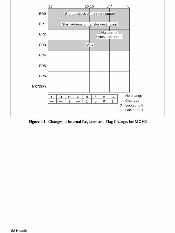
I U H U N Z V C— — 1 — 1 0 0 1
Start address of transfer source
Work
Number ofbytes transferred
: No change: Changes: Locked to 0: Locked to 1
—
↔
01
Start address of transfer destination
Figure 4.1 Changes in Internal Registers and Flag Changes for MOVE
Hitachi 53
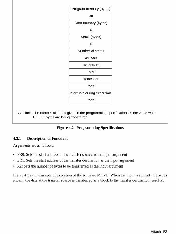
Program memory (bytes)
38
Data memory (bytes)
0
Stack (bytes)
0
Number of states
491580
Re-entrant
Yes
Relocation
Yes
Interrupts during execution
Yes
Caution: The number of states given in the programming specifications is the value whenH'FFFF bytes are being transferred.
Figure 4.2 Programming Specifications
4.3.1 Description of Functions
Arguments are as follows:
• ER0: Sets the start address of the transfer source as the input argument
• ER1: Sets the start address of the transfer destination as the input argument
• R2: Sets the number of bytes to be transferred as the input argument
Figure 4.3 is an example of execution of the software MOVE. When the input arguments are set asshown, the data at the transfer source is transferred as a block to the transfer destination (results).
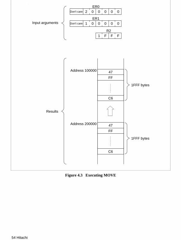
54 Hitachi
Address 100000
C6
47
FF
1FFF bytes
Address 200000
C6
47
FF
1FFF bytes
Results
Input arguments
Don't care
ER0000002
Don't care
ER1000001
R2FFF1
Figure 4.3 Executing MOVE

Hitachi 55
4.3.2 Cautions for Use
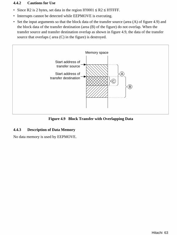
• Since R2 is 2 bytes, set data in the region H'0001 ≤ R2 ≤ H'FFFF.
• Set the input arguments so that the block data of the transfer source (area (A) of figure 4.4) andthe block data of the transfer destination (area (B) of the figure) do not overlap.
• When the transfer source and transfer destination overlap as shown in figure 4.4, the data of thetransfer source that overlaps ( area (C) in the figure) is destroyed.
B
C
AStart address oftransfer destination
Start address oftransfer source
Memory space
Figure 4.4 Block Transfer with Overlapping Data
4.3.3 Description of Data Memory
No data memory is used by MOVE.

56 Hitachi
4.3.4 Examples of Use
After setting the start address of the transfer source, the start address of the transfer destination andthe number of bytes to be transferred, do a subroutine call to MOVE.
Table 4.4 Block Transfer Example (MOVE)
Label Instruction Action
WORK1
.RES. L 1 Reserves the data memory area that sets the startaddress of the transfer source in the user program.
WORK2
.RES. L 1 Reserves the data memory area that sets the startaddress of the transfer destination in the user program.
WORK3
.RES. W 1 Reserves the data memory area that sets the numberof bytes to be transferred in the user program.
MOV. L @WORK1,ER0 Sets the start address of the transfer source as set inthe user program as an input argument.
MOV. L @WORK2,ER1 Sets the start address of the transfer destination as setin the user program as an input argument.
MOV. L @WORK3, R2 Sets the number of bytes to be transferred as set in theuser program as an input argument.
@MOVEJSR
Subroutine call to MOVE.
4.3.5 Principles of Operation
• When the data to be transferred is 4 bytes or more, the MOV.L instruction is used to do repeatedtransfers in 4-byte units.
• When the data to be transferred is less than 4 bytes, the software switches to the MOV.Binstruction to do transfers in byte units.
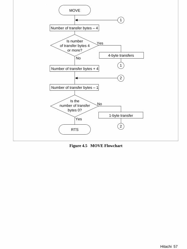
Hitachi 57
2
2
1
1
Yes
Yes
No
No
RTS
Is thenumber of transfer
bytes 0?
Number of transfer bytes – 1
Number of transfer bytes + 4
Is numberof transfer bytes 4
or more?
Number of transfer bytes – 4
MOVE
4-byte transfers
1-byte transfer
Figure 4.5 MOVE Flowchart

58 Hitachi
4.3.6 Program Listing

Hitachi 59
4.4 Block Transfer Using Block Transfer Instruction
MCU: H8/300H Series
Label Name: EEPMOV
Functions Used: EEPMOV.W Instruction
Function: Transfers block data (up to 65535 bytes) to any even address using the block transferinstruction (EEPMOV.W).
Table 4.5 EEPMOV Arguments
Contents Storage Location Data Length (Bytes)
Input Start address of transfer source ER5 4
Start address of transfer destination ER6 4
Number of bytes transferred R4 2
Output — — —
60 Hitachi
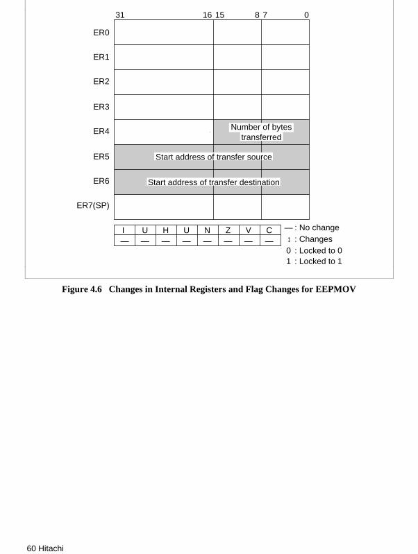
ER0
ER1
ER2
ER3
ER4
ER5
ER6
ER7(SP)
31 1516 78 0
I U H U N Z V C— — — — — — — —
Start address of transfer source
Start address of transfer destination
: No change: Changes: Locked to 0: Locked to 1
—
↔
01
Number of bytestransferred
Figure 4.6 Changes in Internal Registers and Flag Changes for EEPMOV

Hitachi 61
4
0
0
262148
Program memory (bytes)
Data memory (bytes)
Stack (bytes)
Number of states
Re-entrant
Yes
Relocation
Yes
Interrupts during execution
Yes
Caution: The number of states given in the programming specifications is the value whenH'FFFF bytes are being transferred.
Figure 4.7 Programming Specifications
62 Hitachi
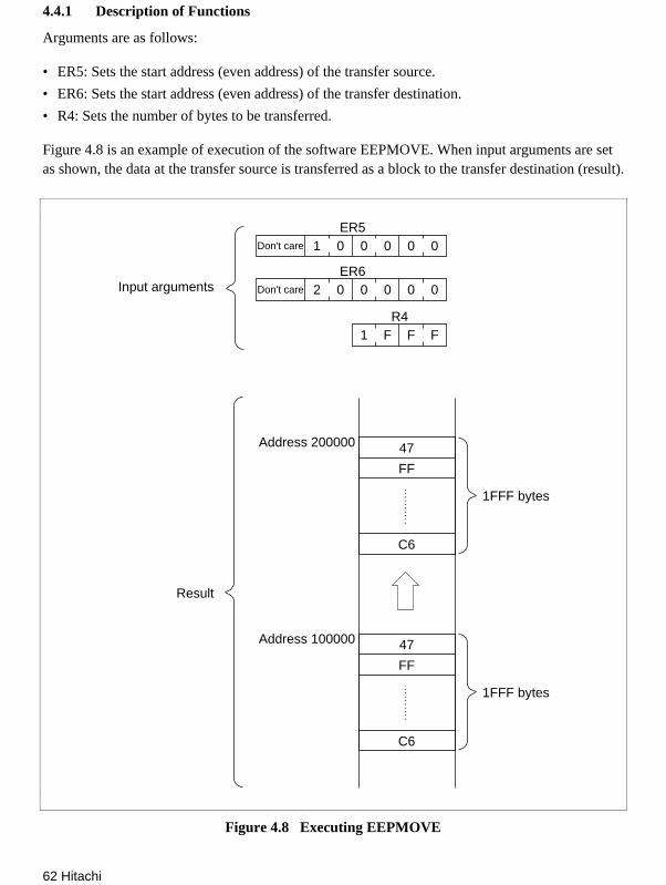
4.4.1 Description of Functions
Arguments are as follows:
• ER5: Sets the start address (even address) of the transfer source.
• ER6: Sets the start address (even address) of the transfer destination.
• R4: Sets the number of bytes to be transferred.
Figure 4.8 is an example of execution of the software EEPMOVE. When input arguments are setas shown, the data at the transfer source is transferred as a block to the transfer destination (result).
Address 200000
C6
47
FF
1FFF bytes
Address 100000
C6
47
FF
1FFF bytes
Result
Input arguments
Don't care
ER5000001
Don't care
ER6000002
R4FFF1
Figure 4.8 Executing EEPMOVE
Hitachi 63
4.4.2 Cautions for Use
• Since R2 is 2 bytes, set data in the region H'0001 ≤ R2 ≤ H'FFFF.
• Interrupts cannot be detected while EEPMOVE is executing.
• Set the input arguments so that the block data of the transfer source (area (A) of figure 4.9) andthe block data of the transfer destination (area (B) of the figure) do not overlap. When thetransfer source and transfer destination overlap as shown in figure 4.9, the data of the transfersource that overlaps ( area (C) in the figure) is destroyed.
B
C
AStart address oftransfer destination
Start address oftransfer source
Memory space
Figure 4.9 Block Transfer with Overlapping Data
4.4.3 Description of Data Memory
No data memory is used by EEPMOVE.

64 Hitachi
4.4.4 Examples of Use
After setting the start address of the transfer source, the start address of the transfer destination andthe number of bytes to be transferred, do a subroutine call to EEPMOVE.
Table 4.6 Block Transfer Example (EEPMOVE).
Label Instruction Action
WORK1
RES. L 1 Reserves the data memory area that sets the startaddress of the transfer source in the user program.
WORK2
RES. L 1 Reserves the data memory area that sets the startaddress of the transfer destination in the userprogram.
WORK3
RES. W 1 Reserves the data memory area that sets the numberof bytes to be transferred in the user program.
MOV. L @WORK1,ER5 Sets the start address of the transfer source as set inthe user program as an input argument.
MOV. L @WORK2,ER6 Sets the start address of the transfer destination as setin the user program as an input argument.
MOV. L @WORK3, R4 Sets the number of bytes to be transferred as set inthe user program as an input argument.
@EEPMOVJSR
Subroutine call to EEPMOVE.
4.4.5 Principles of Operation
Use the block transfer instruction (EEPMOV.W).
RTS
Blocks are transferredusing the block transfer
instruction (EEPMOV.W)
EEPMOV
Figure 4.10 EEPMOV Flowchart
Hitachi 65
4.4.6 Program Listing
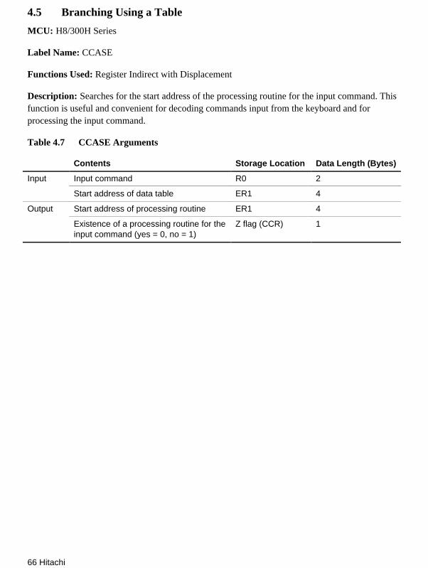
66 Hitachi
4.5 Branching Using a Table
MCU: H8/300H Series
Label Name: CCASE
Functions Used: Register Indirect with Displacement
Description: Searches for the start address of the processing routine for the input command. Thisfunction is useful and convenient for decoding commands input from the keyboard and forprocessing the input command.
Table 4.7 CCASE Arguments
Contents Storage Location Data Length (Bytes)
Input Input command R0 2
Start address of data table ER1 4
Output Start address of processing routine ER1 4
Existence of a processing routine for theinput command (yes = 0, no = 1)
Z flag (CCR) 1

Hitachi 67
WorkER0
ER1
ER2
ER3
ER4
ER5
ER6
ER7(SP)
31 1516 78 0
I U H U N Z V C— — — 0
Input command
—
↔
01
↔↔↔
Start address of data table,start address of processing routine
: No change: Changes: Locked to 0: Locked to 1
↔
Figure 4.11 Changes in Internal Registers and Flag Changes for CCASE
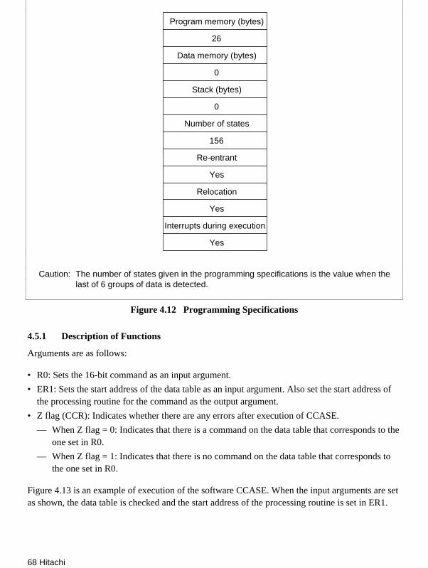
68 Hitachi
26
0
0
156
Program memory (bytes)
Data memory (bytes)
Stack (bytes)
Number of states
Re-entrant
Yes
Relocation
Yes
Interrupts during execution
Yes
Caution: The number of states given in the programming specifications is the value when thelast of 6 groups of data is detected.
Figure 4.12 Programming Specifications
4.5.1 Description of Functions
Arguments are as follows:
• R0: Sets the 16-bit command as an input argument.
• ER1: Sets the start address of the data table as an input argument. Also set the start address ofthe processing routine for the command as the output argument.
• Z flag (CCR): Indicates whether there are any errors after execution of CCASE.
— When Z flag = 0: Indicates that there is a command on the data table that corresponds to theone set in R0.
— When Z flag = 1: Indicates that there is no command on the data table that corresponds tothe one set in R0.
Figure 4.13 is an example of execution of the software CCASE. When the input arguments are setas shown, the data table is checked and the start address of the processing routine is set in ER1.
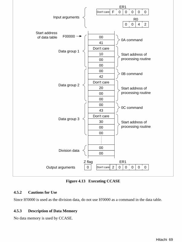
Hitachi 69
00
410A command
Input arguments
Don't care
ER100000F
R02400
Don't care
10
00
00
00
42
Don't care
20
00
00
00
43
Don't care
30
00
00
00
00
Start addressof data table
Data group 1
Data group 2
Data group 3
Division data
Start address ofprocessing routine
0B command
0C command
Start address ofprocessing routine
Start address ofprocessing routine
Don't care
ER1
000002
Z flag
Output arguments 0
F00000
Figure 4.13 Executing CCASE
4.5.2 Cautions for Use
Since H'0000 is used as the division data, do not use H'0000 as a command in the data table.
4.5.3 Description of Data Memory
No data memory is used by CCASE.

70 Hitachi
4.5.4 Examples of Use
After setting the command and the start address of the data table, do a subroutine call to CCASE.
Table 4.8 Block Transfer Example (CCASE)
Label Instruction Action
WORK 1 .RES. W 1 Reserves the data memory area that sets thecommand in the user program.
WORK 2 .RES. L 1 Reserves the data memory area that sets the startaddress of the data table in the user program.
MOV. L @WORK2,ER1 Sets the start address of the data table as set in theuser program as an input argument.
MOV. W @WORK1,R0 Sets the command set in the user program as aninput argument.
@CCASEJSR
Subroutine call of CCASE
BEQ ERROR When there is no command in the data table thatcorresponds to the command input, the routinebranches to an error program.
ERROR
Program that branches tothe processing routine*
Error program

Hitachi 71
Table 4.8 Block Transfer Example (CCASE) (cont)
Label Instruction Action
DTABLE .ORG H’F000 Start address of data table
.DATA.W
H’0041 0A command
.DATA.W
H’F100 Start address of processing routine for 0A command
.DATA.W
H’0042 0B command
.DATA.W
H’F200 Start address of processing routine for 0B command
.DATA.W
H’0000 Division data
@CCASEJSR
Subroutine call of CCASE
BEQ ERROR Branches to ERROR when the Z flag is set
↑Bran-ches topro-cessingroutine↓
JMP @ER1 Jumps to processing routine
ERROR
Error program
Note: Example of program that branches to a processing routine: CCASE only sets the startaddress of the processing routine in ER. When actually branching to a processing routine,create a program like that shown below.
4.5.5 Principles of Operation
• ER1 is used as a pointer to the address storing the command on the data table.
• The command at the address indicated in ER1 of the data table is set in E0 and compared to theinput command.
• When the input command and the data table command match, the start address of the processingroutine located after the command is set, the Z flag is cleared and CCASE ends.

72 Hitachi
• When H'0000 is detected (indicating the end of the data table), the Z flag is set and CCASEends.
1
Yes
No
RTS
Clear the Z flag
End of datatable?
The first command in thedata table is set in E0
CCASE
Set the start address of theprocessing routine in ER1
No
Yes
1
The next command isset in ER1
ER1 is incremented to theaddress where the next
command is stored
Same command?
Figure 4.14 CCASE Flowchart

Hitachi 73
4.5.6 Program Listing
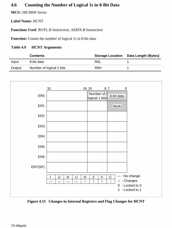
74 Hitachi
4.6 Counting the Number of Logical 1s in 8-Bit Data
MCU: H8/300H Series
Label Name: HCNT
Functions Used: ROTL.B Instruction, ADDX.B Instruction
Function: Counts the number of logical 1s in 8-bit data.
Table 4.9 HCNT Arguments
Contents Storage Location Data Length (Bytes)
Input 8-bit data R0L 1
Output Number of logical 1 bits R0H 1
ER0
ER1
ER2
ER3
ER4
ER5
ER6
ER7(SP)
31 1516 78 0
I U H U N Z V C— — — ↔↔↔
Work
— ↔
Number oflogical 1 bits
8-bit data
—
↔
01
: No change: Changes: Locked to 0: Locked to 1
Figure 4.15 Changes in Internal Registers and Flag Changes for HCNT

Hitachi 75
16
0
0
126
Program memory (bytes)
Data memory (bytes)
Stack (bytes)
Number of states
Re-entrant
Yes
Relocation
Yes
Interrupts during execution
Yes
Caution: The number of states given in the programming specifications is the value when the 8-bit data is H'FF.
Figure 4.16 Programming Specifications
4.6.1 Description of Functions
Arguments are as follows:
• R0L: Sets the 8-bit data.
• R0H: Sets the number of bits of logical 1s in the 8-bit data.
Figure 4.17 is an example of execution of the software HNCT. When the input arguments are setas shown, the number of bits of logical 1s are set in R0H.
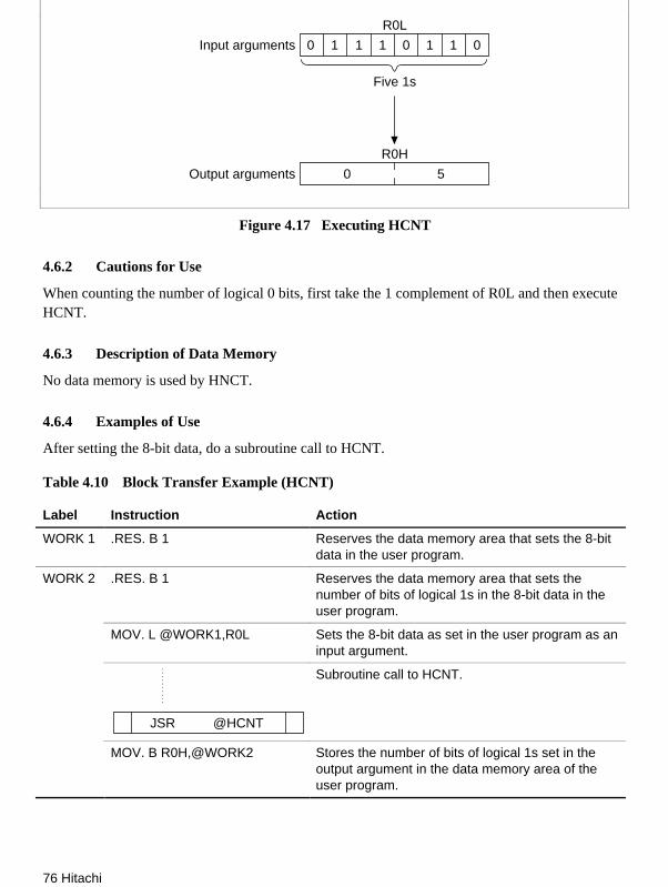
76 Hitachi
R0L
01101110
Five 1s
R0H
50Output arguments
Input arguments
Figure 4.17 Executing HCNT
4.6.2 Cautions for Use
When counting the number of logical 0 bits, first take the 1 complement of R0L and then executeHCNT.
4.6.3 Description of Data Memory
No data memory is used by HNCT.
4.6.4 Examples of Use
After setting the 8-bit data, do a subroutine call to HCNT.
Table 4.10 Block Transfer Example (HCNT)
Label Instruction Action
WORK 1 .RES. B 1 Reserves the data memory area that sets the 8-bitdata in the user program.
WORK 2 .RES. B 1 Reserves the data memory area that sets thenumber of bits of logical 1s in the 8-bit data in theuser program.
MOV. L @WORK1,R0L Sets the 8-bit data as set in the user program as aninput argument.
@HCNTJSR
Subroutine call to HCNT.
MOV. B R0H,@WORK2 Stores the number of bits of logical 1s set in theoutput argument in the data memory area of theuser program.

Hitachi 77
4.6.5 Principles of Operation
• The rotate instruction (ROTL.B) is used and the 8-bit data (R0L) is set 1 bit at a time in the Cbit.
• When the logical 1 counter (R0H) is added to 0 using the add instruction with carry (ADDX.B),1 is added to the logical 1 counter if the C bit is 1 and 0 is added to the logical 1 counter if the Cbit is 0.
• The two steps above are repeated until the rotate counter (R1L) becomes 0, which reveals thenumber of logical 1s in the 8-bit data.

78 Hitachi
Yes
No
RTS
Rotate counter = 0?
The rotate counter is set to 8 (R1L)
HCNT
To return the 8-bit data to its inputstate, it is shifted 1 bit to the left
The rotate counter (R1L)is decremented
The MSB of the 8-bit data(R0L) is set to the C bit
The logical 1 counter (R0H)is added to the C bit
The logical 1 counter(R0H) is cleared
Figure 4.18 HCNT Flowchart

Hitachi 79
4.6.6 Program Listing
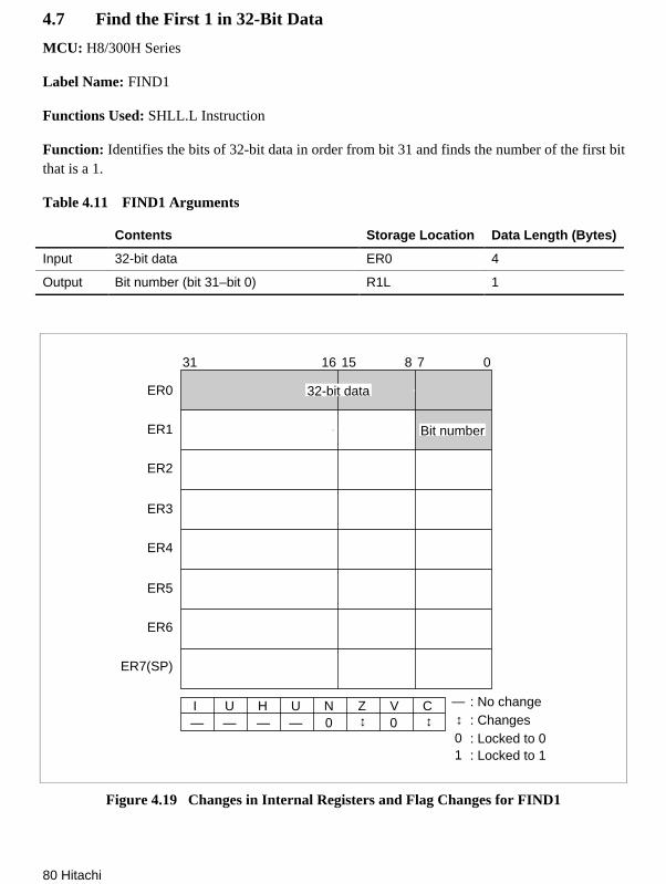
80 Hitachi
4.7 Find the First 1 in 32-Bit Data
MCU: H8/300H Series
Label Name: FIND1
Functions Used: SHLL.L Instruction
Function: Identifies the bits of 32-bit data in order from bit 31 and finds the number of the first bitthat is a 1.
Table 4.11 FIND1 Arguments
Contents Storage Location Data Length (Bytes)
Input 32-bit data ER0 4
Output Bit number (bit 31–bit 0) R1L 1
ER0
ER1
ER2
ER3
ER4
ER5
ER6
ER7(SP)
31 1516 78 0
I U H U N Z V C— — — 0 ↔↔
Bit number
— 0
—
↔
01
: No change: Changes: Locked to 0: Locked to 1
32-bit data
Figure 4.19 Changes in Internal Registers and Flag Changes for FIND1
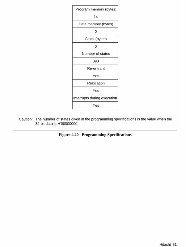
Hitachi 81
14
0
0
398
Program memory (bytes)
Data memory (bytes)
Stack (bytes)
Number of states
Re-entrant
Yes
Relocation
Yes
Interrupts during execution
Yes
Caution: The number of states given in the programming specifications is the value when the32-bit data is H'00000000.
Figure 4.20 Programming Specifications

82 Hitachi
4.7.1 Description of Functions
Arguments are as follows:
• ER0: Sets the 32-bit data.
• R1L: Sets the number of the first bit found to have a 1 (bit 31 to bit 0).
Figure 4.21 s an example of execution of the software FIND1. When the input arguments are setas shown, the number of the first bit with a 1 is set in R1L.
Bit 3100010000
Bit number
B1Output
arguments
Input arguments 10100010 00110111 0110111
Bit 27 Bit 01ER0
R1L
Figure 4.21 Executing FIND1
4.7.2 Cautions for Use
When the 32-bit data is H'00000000, H'FF is set as the bit number (R1L).
4.7.3 Description of Data Memory
No data memory is used by FIND1.
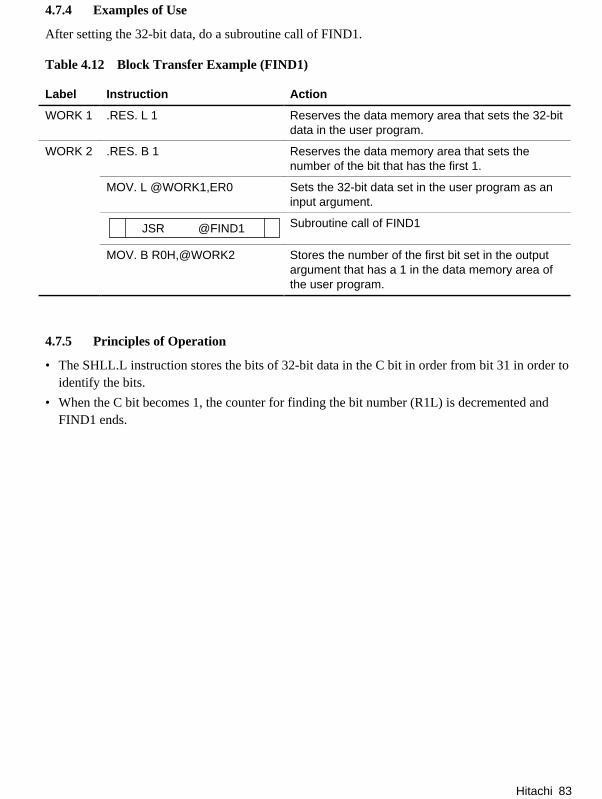
Hitachi 83
4.7.4 Examples of Use
After setting the 32-bit data, do a subroutine call of FIND1.
Table 4.12 Block Transfer Example (FIND1)
Label Instruction Action
WORK 1 .RES. L 1 Reserves the data memory area that sets the 32-bitdata in the user program.
WORK 2 .RES. B 1 Reserves the data memory area that sets thenumber of the bit that has the first 1.
MOV. L @WORK1,ER0 Sets the 32-bit data set in the user program as aninput argument.
@FIND1JSR Subroutine call of FIND1
MOV. B R0H,@WORK2 Stores the number of the first bit set in the outputargument that has a 1 in the data memory area ofthe user program.
4.7.5 Principles of Operation
• The SHLL.L instruction stores the bits of 32-bit data in the C bit in order from bit 31 in order toidentify the bits.
• When the C bit becomes 1, the counter for finding the bit number (R1L) is decremented andFIND1 ends.
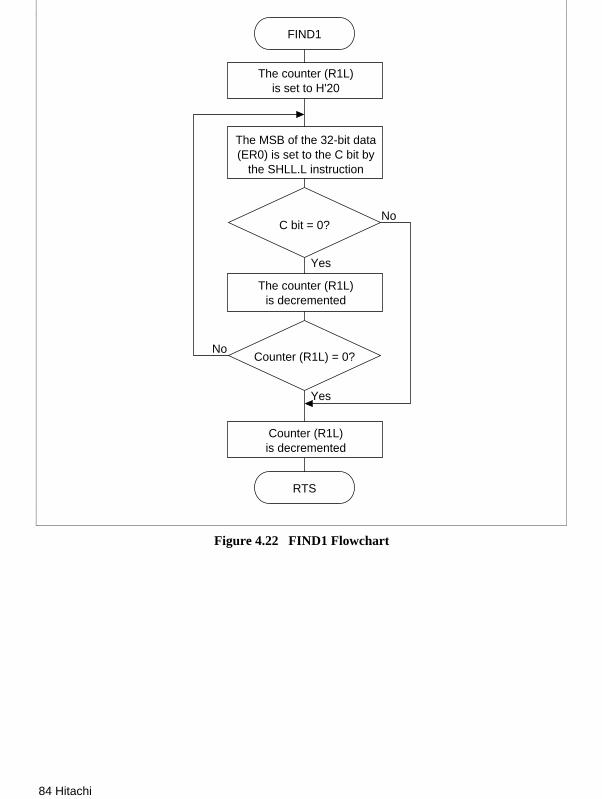
84 Hitachi
Yes
No
The counter (R1L)is set to H'20
FIND1
The MSB of the 32-bit data(ER0) is set to the C bit by
the SHLL.L instruction
The counter (R1L)is decremented
Counter (R1L)is decremented
RTS
C bit = 0?
Yes
No
Counter (R1L) = 0?
Figure 4.22 FIND1 Flowchart

Hitachi 85
4.7.6 Program Listing
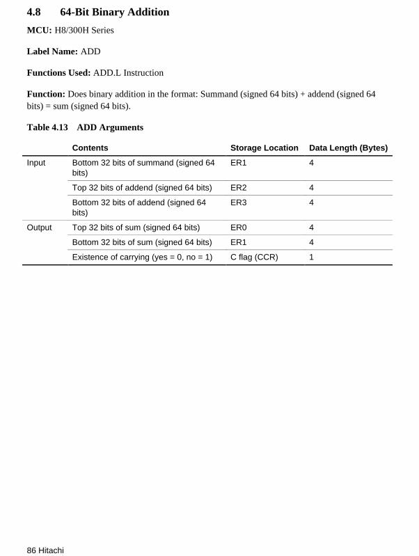
86 Hitachi
4.8 64-Bit Binary Addition
MCU: H8/300H Series
Label Name: ADD
Functions Used: ADD.L Instruction
Function: Does binary addition in the format: Summand (signed 64 bits) + addend (signed 64bits) = sum (signed 64 bits).
Table 4.13 ADD Arguments
Contents Storage Location Data Length (Bytes)
Input Bottom 32 bits of summand (signed 64bits)
ER1 4
Top 32 bits of addend (signed 64 bits) ER2 4
Bottom 32 bits of addend (signed 64bits)
ER3 4
Output Top 32 bits of sum (signed 64 bits) ER0 4
Bottom 32 bits of sum (signed 64 bits) ER1 4
Existence of carrying (yes = 0, no = 1) C flag (CCR) 1
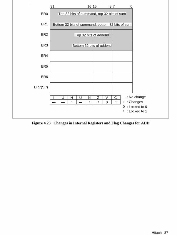
Hitachi 87
ER0
ER1
ER2
ER3
ER4
ER5
ER6
ER7(SP)
31 1516 78 0
I U H U N Z V C— — — 0
Top 32 bits of summand, top 32 bits of sum
Bottom 32 bits of summand, bottom 32 bits of sum
Bottom 32 bits of addend
Top 32 bits of addend
↔ ↔ ↔ ↔
—
↔
01
: No change: Changes: Locked to 0: Locked to 1
Figure 4.23 Changes in Internal Registers and Flag Changes for ADD
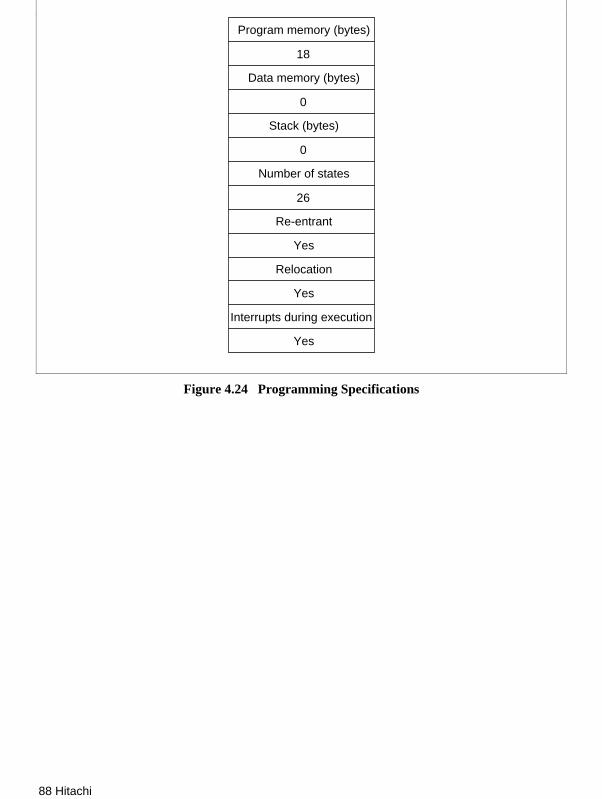
88 Hitachi
18
0
0
26
Program memory (bytes)
Data memory (bytes)
Stack (bytes)
Number of states
Re-entrant
Yes
Relocation
Yes
Interrupts during execution
Yes
Figure 4.24 Programming Specifications
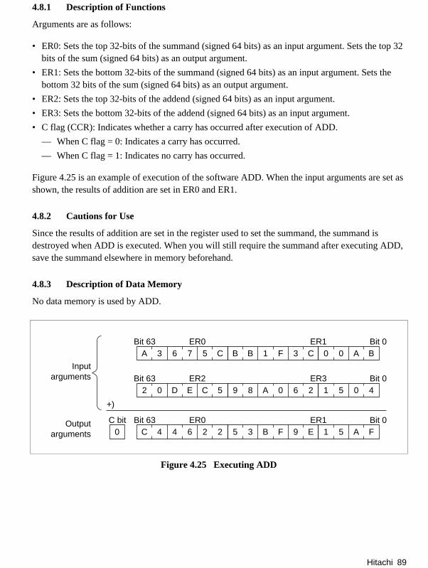
Hitachi 89
4.8.1 Description of Functions
Arguments are as follows:
• ER0: Sets the top 32-bits of the summand (signed 64 bits) as an input argument. Sets the top 32bits of the sum (signed 64 bits) as an output argument.
• ER1: Sets the bottom 32-bits of the summand (signed 64 bits) as an input argument. Sets thebottom 32 bits of the sum (signed 64 bits) as an output argument.
• ER2: Sets the top 32-bits of the addend (signed 64 bits) as an input argument.
• ER3: Sets the bottom 32-bits of the addend (signed 64 bits) as an input argument.
• C flag (CCR): Indicates whether a carry has occurred after execution of ADD.
— When C flag = 0: Indicates a carry has occurred.
— When C flag = 1: Indicates no carry has occurred.
Figure 4.25 is an example of execution of the software ADD. When the input arguments are set asshown, the results of addition are set in ER0 and ER1.
4.8.2 Cautions for Use
Since the results of addition are set in the register used to set the summand, the summand isdestroyed when ADD is executed. When you will still require the summand after executing ADD,save the summand elsewhere in memory beforehand.
4.8.3 Description of Data Memory
No data memory is used by ADD.
Bit 63C5763A
ER1C3F1BB
Bit 0BA00
ER0
Bit 635CED02
ER3260A89
Bit 04051
ER2
Bit 6322644C
ER1E9FB35
Bit 0FA51
ER00
C bit
+)
Outputarguments
Inputarguments
Figure 4.25 Executing ADD

90 Hitachi
4.8.4 Examples of Use
After setting the summand and addend, does a subroutine call to ADD.
Table 4.14 Block Transfer Example (ADD)
Label Instruction Action
WORK 1 .RES. L 1 Reserves the data memory area that sets thetop 32-bits of the summand (signed 64 bits) inthe user program.
WORK 2 .RES. L 1 Reserves the data memory area that sets thebottom 32-bits of the summand (signed 64 bits)in the user program.
WORK 3 .RES. L 1 Reserves the data memory area that sets thetop 32-bits of the addend (signed 64 bits) in theuser program.
WORK 4 .RES. L 1 Reserves the data memory area that sets thebottom 32-bits of the addend (signed 64 bits) inthe user program.
MOV. L @WORK1,ER0 Set as the input argument the top 32-bits of thesummand set in the user program.
MOV. L @WORK2,ER1 Set as the input argument the bottom 32-bits ofthe summand set in the user program.
MOV. L @WORK3,ER2 Set as the input argument the top 32-bits of theaddend set in the user program.
MOV. L @WORK4,ER3 Set as the input argument the bottom 32-bits ofthe addend set in the user program.
@ADDJSR
OVERBCS
Processing routine for carrying overOVER
Subroutine call to ADD.
When carrying occurs, the routine branches tothe processing routine for carrying.

Hitachi 91
4.8.5 Principles of Operation
• Bits 0–31 are added using the ADD.L instruction.
• Bits 32–63 are added in 1-byte units from the bottom using the addition instruction withcarrying (ADDX.B), which can handle carrying. Since bits 48–55 are on the extended register,the addition instruction with carry is transferred into a usable general register and addition isthen performed.
RTS
Bits 0–31 added usingthe ADD.L instruction
ADD
Bits 32–39 added usingthe ADDX.B instruction
Bits 40–47 added usingthe ADDX.B instruction
Top 16 bits of the summandtransferred to general register (R2)
Top 16 bits of the addendtransferred to general register (R3)
Bits 48–55 added usingthe ADDX.B instruction
Bits 56–63 added usingthe ADDX.B instruction
Figure 4.26 ADD Flowchart

92 Hitachi
4.8.6 Program Listing

Hitachi 93
4.9 64-Bit Binary Subtraction
MCU: H8/300H Series
Label Name: SUB
Functions Used: SUB.L Instruction
Function: Does binary subtraction in the format: minuend (signed 64 bits) – subtrahend (signed64 bits) = difference (signed 64 bits).
Table 4.15 SUB Arguments
Contents Storage Location Data Length (Bytes)
Input Top 32 bits of minuend (signed 64 bits) ER0 4
Bottom 32 bits of minuend (signed 64bits)
ER1 4
Top 32 bits of subtrahend (signed 64bits)
ER2 4
Bottom 32 bits of subtrahend (signed 64bits)
ER3 4
Output Top 32 bits of difference (signed 64 bits) ER0 4
Bottom 32 bits of difference (signed 64bits)
ER1 4
Existence of carrying C flag (CCR) 1
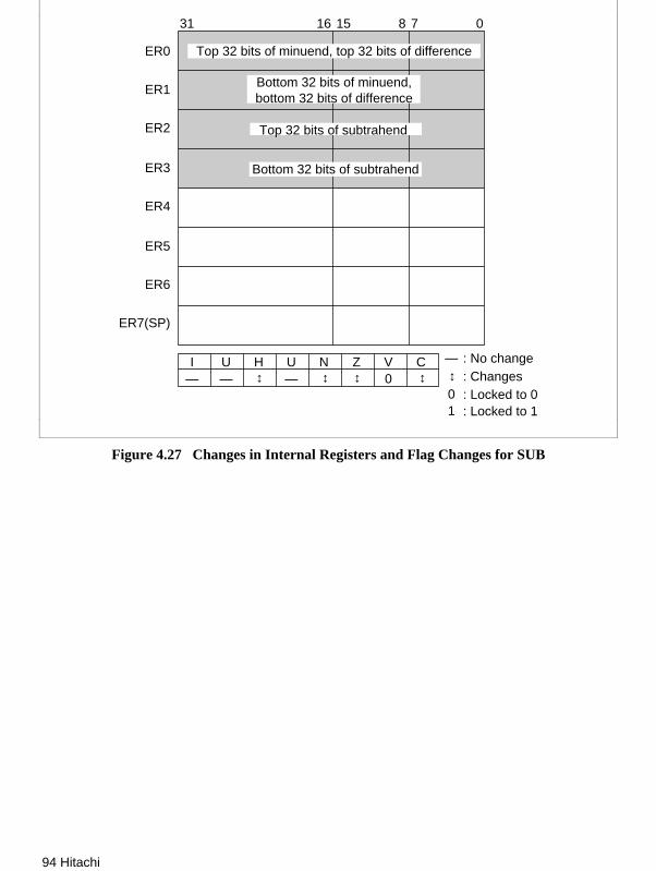
94 Hitachi
ER0
ER1
ER2
ER3
ER4
ER5
ER6
ER7(SP)
31 1516 78 0
I U H U N Z V C— — — 0
Top 32 bits of minuend, top 32 bits of difference
Bottom 32 bits of minuend,bottom 32 bits of difference
Bottom 32 bits of subtrahend
Top 32 bits of subtrahend
↔ ↔ ↔ ↔
—
↔
01
: No change: Changes: Locked to 0: Locked to 1
Figure 4.27 Changes in Internal Registers and Flag Changes for SUB

Hitachi 95
18
0
0
26
Program memory (bytes)
Data memory (bytes)
Stack (bytes)
Number of states
Re-entrant
Yes
Relocation
Yes
Interrupts during execution
Yes
Figure 4.28 Programming Specifications
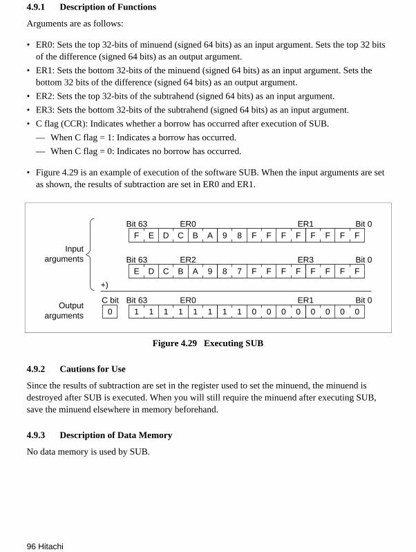
96 Hitachi
4.9.1 Description of Functions
Arguments are as follows:
• ER0: Sets the top 32-bits of minuend (signed 64 bits) as an input argument. Sets the top 32 bitsof the difference (signed 64 bits) as an output argument.
• ER1: Sets the bottom 32-bits of the minuend (signed 64 bits) as an input argument. Sets thebottom 32 bits of the difference (signed 64 bits) as an output argument.
• ER2: Sets the top 32-bits of the subtrahend (signed 64 bits) as an input argument.
• ER3: Sets the bottom 32-bits of the subtrahend (signed 64 bits) as an input argument.
• C flag (CCR): Indicates whether a borrow has occurred after execution of SUB.
— When C flag = 1: Indicates a borrow has occurred.
— When C flag = 0: Indicates no borrow has occurred.
• Figure 4.29 is an example of execution of the software SUB. When the input arguments are setas shown, the results of subtraction are set in ER0 and ER1.
Bit 63ABCDEF
ER1FFFF89
Bit 0FFFF
ER0
Bit 639ABCDE
ER3FFFF78
Bit 0FFFF
ER2
Bit 63111111
ER1000011
Bit 00000
ER00
C bit
+)
Outputarguments
Inputarguments
Figure 4.29 Executing SUB
4.9.2 Cautions for Use
Since the results of subtraction are set in the register used to set the minuend, the minuend isdestroyed after SUB is executed. When you will still require the minuend after executing SUB,save the minuend elsewhere in memory beforehand.
4.9.3 Description of Data Memory
No data memory is used by SUB.
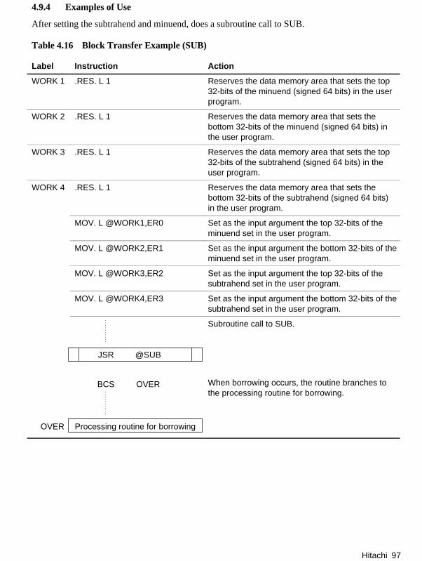
Hitachi 97
4.9.4 Examples of Use
After setting the subtrahend and minuend, does a subroutine call to SUB.
Table 4.16 Block Transfer Example (SUB)
Label Instruction Action
WORK 1 .RES. L 1 Reserves the data memory area that sets the top32-bits of the minuend (signed 64 bits) in the userprogram.
WORK 2 .RES. L 1 Reserves the data memory area that sets thebottom 32-bits of the minuend (signed 64 bits) inthe user program.
WORK 3 .RES. L 1 Reserves the data memory area that sets the top32-bits of the subtrahend (signed 64 bits) in theuser program.
WORK 4 .RES. L 1 Reserves the data memory area that sets thebottom 32-bits of the subtrahend (signed 64 bits)in the user program.
MOV. L @WORK1,ER0 Set as the input argument the top 32-bits of theminuend set in the user program.
MOV. L @WORK2,ER1 Set as the input argument the bottom 32-bits of theminuend set in the user program.
MOV. L @WORK3,ER2 Set as the input argument the top 32-bits of thesubtrahend set in the user program.
MOV. L @WORK4,ER3 Set as the input argument the bottom 32-bits of thesubtrahend set in the user program.
@SUBJSR
OVERBCS
Processing routine for borrowingOVER
Subroutine call to SUB.
When borrowing occurs, the routine branches tothe processing routine for borrowing.

98 Hitachi
4.9.5 Principles of operation
• Bits 0–31 are subtracted using the SUB.L instruction.
• Bits 32–63 are subtracted in 1-byte units from the bottom using the subtraction instruction withcarrying (SUBX.B), which can handle borrowing. Since bits 48–55 are in the extended register,the subtraction instruction with borrow is transferred into the usable general register andsubtraction is then performed.
RTS
Bits 0–31 subtracted usingthe SUB.L instruction
SUB
Bits 32–39 subtracted usingthe SUBX.B instruction
Bits 40–47 subtracted usingthe SUBX.B instruction
Top 16 bits of the minuendtransferred to the general register (R2)
Top 16 bits of the subtrahendtransferred to the general register (R3)
Bits 48–55 subtracted usingthe SUBX.B instruction
Bits 56–63 subtracted usingthe SUBX.B instruction
Figure 4.30 SUB Flowchart

Hitachi 99
4.9.6 Program Listing
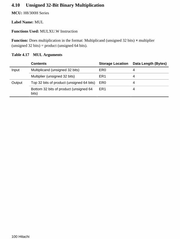
100 Hitachi
4.10 Unsigned 32-Bit Binary Multiplication
MCU: H8/300H Series
Label Name: MUL
Functions Used: MULXU.W Instruction
Function: Does multiplication in the format: Multiplicand (unsigned 32 bits) × multiplier(unsigned 32 bits) = product (unsigned 64 bits).
Table 4.17 MUL Arguments
Contents Storage Location Data Length (Bytes)
Input Multiplicand (unsigned 32 bits) ER0 4
Multiplier (unsigned 32 bits) ER1 4
Output Top 32 bits of product (unsigned 64 bits) ER0 4
Bottom 32 bits of product (unsigned 64bits)
ER1 4

Hitachi 101
ER0
ER1
ER2
ER3
ER4
ER5
ER6
ER7(SP)
31 1516 78 0
I U H U N Z V C— — —
Work
Work
—
↔
01
↔ ↔ ↔ ↔↔
: No change: Changes: Locked to 0: Locked to 1
MultiplicandTop 32 bits of product
MultiplierBottom 32 bits of product
Figure 4.31 Changes in Internal Registers and Flag Changes for MUL

102 Hitachi
34
0
0
126
Program memory (bytes)
Data memory (bytes)
Stack (bytes)
Number of states
Re-entrant
Yes
Relocation
Yes
Interrupts during execution
Yes
Caution: The number of states in the programming specifications is the value when calculatingas H'FFFFFFFF x H'FFFFFFFF.
Figure 4.32 Programming Specifications
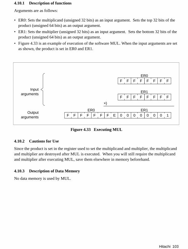
Hitachi 103
4.10.1 Description of functions
Arguments are as follows:
• ER0: Sets the multiplicand (unsigned 32 bits) as an input argument. Sets the top 32 bits of theproduct (unsigned 64 bits) as an output argument.
• ER1: Sets the multiplier (unsigned 32 bits) as an input argument. Sets the bottom 32 bits of theproduct (unsigned 64 bits) as an output argument.
• Figure 4.33 is an example of execution of the software MUL. When the input arguments are setas shown, the product is set in ER0 and ER1.
ER0FFFF FFFF
ER1FFFF FFFF
FFFFFFER10000EF 1000
ER0
×)
Outputarguments
Inputarguments
Figure 4.33 Executing MUL
4.10.2 Cautions for Use
Since the product is set in the register used to set the multiplicand and multiplier, the multiplicandand multiplier are destroyed after MUL is executed. When you will still require the multiplicandand multiplier after executing MUL, save them elsewhere in memory beforehand.
4.10.3 Description of Data Memory
No data memory is used by MUL.

104 Hitachi
4.10.4 Examples of Use
After setting the multiplicand and multiplier, do a subroutine call to MUL.
Table 4.18 Block Transfer Example (MUL)
Label Instruction Action
WORK 1 .RES. L 1 Reserves the data memory area that sets themultiplicand (unsigned 32 bits) in the user program.
WORK 2 .RES. L 1 Reserves the data memory area that sets themultiplier (unsigned 32 bits) in the user program.
MOV. L @WORK1,ER0 Sets as the input argument the 32-bit binarymultiplicand set in the user program.
MOV. L @WORK2,ER1 Sets as the input argument the 32-bit binarymultiplier set in the user program.
@MULJSR Subroutine call to MUL.
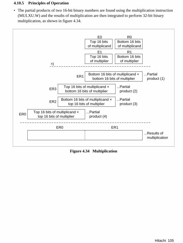
Hitachi 105
4.10.5 Principles of Operation
• The partial products of two 16-bit binary numbers are found using the multiplication instruction(MULXU.W) and the results of multiplication are then integrated to perform 32-bit binarymultiplication, as shown in figure 4.34.
Bottom 16 bits of multiplicand
R0E0
ER1
×)
...Partial product (1)
ER1ER0
Top 16 bits of multiplicand
Bottom 16 bits of multiplier
R1E1Top 16 bits of multiplier
Bottom 16 bits of multiplicand ×bottom 16 bits of multiplier
ER3...Partial product (2)
Top 16 bits of multiplicand ×bottom 16 bits of multiplier
ER2...Partial product (3)
Bottom 16 bits of multiplicand ×top 16 bits of multiplier
ER0...Partial product (4)
Top 16 bits of multiplicand ×top 16 bits of multiplier
...Results of multiplication
Figure 4.34 Multiplication
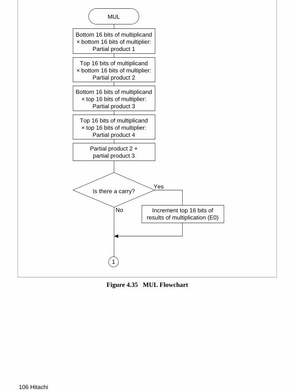
106 Hitachi
1
Yes
No
Is there a carry?
Bottom 16 bits of multiplicand× bottom 16 bits of multiplier:
Partial product 1
MUL
Top 16 bits of multiplicand× bottom 16 bits of multiplier:
Partial product 2
Bottom 16 bits of multiplicand× top 16 bits of multiplier:
Partial product 3
Top 16 bits of multiplicand× top 16 bits of multiplier:
Partial product 4
Partial product 2 +partial product 3
Increment top 16 bits ofresults of multiplication (E0)
Figure 4.35 MUL Flowchart
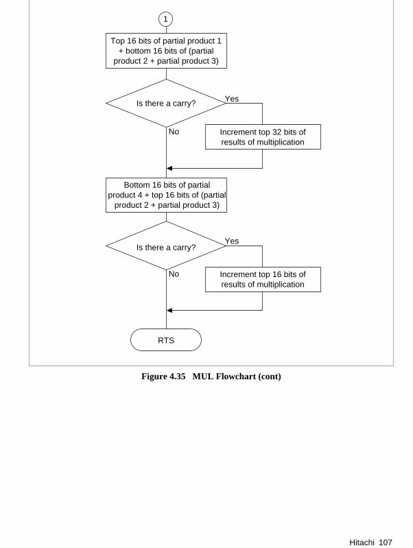
Hitachi 107
1
Yes
No
Is there a carry?
Top 16 bits of partial product 1+ bottom 16 bits of (partial
product 2 + partial product 3)
RTS
Bottom 16 bits of partialproduct 4 + top 16 bits of (partial
product 2 + partial product 3)
Increment top 16 bits ofresults of multiplication
Yes
No Increment top 32 bits ofresults of multiplication
Is there a carry?
Figure 4.35 MUL Flowchart (cont)

108 Hitachi
4.10.6 Program Listing
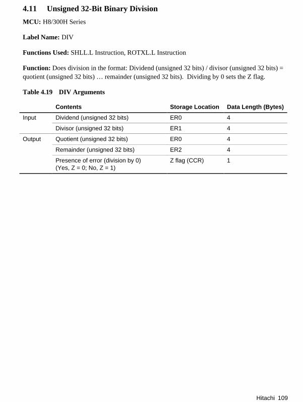
Hitachi 109
4.11 Unsigned 32-Bit Binary Division
MCU: H8/300H Series
Label Name: DIV
Functions Used: SHLL.L Instruction, ROTXL.L Instruction
Function: Does division in the format: Dividend (unsigned 32 bits) / divisor (unsigned 32 bits) =quotient (unsigned 32 bits) … remainder (unsigned 32 bits). Dividing by 0 sets the Z flag.
Table 4.19 DIV Arguments
Contents Storage Location Data Length (Bytes)
Input Dividend (unsigned 32 bits) ER0 4
Divisor (unsigned 32 bits) ER1 4
Output Quotient (unsigned 32 bits) ER0 4
Remainder (unsigned 32 bits) ER2 4
Presence of error (division by 0)(Yes, Z = 0; No, Z = 1)
Z flag (CCR) 1

110 Hitachi
ER0
ER1
ER2
ER3
ER4
ER5
ER6
ER7(SP)
31 1516 78 0
I U H U N Z V C— — —
Divisor
Work
Remainder
↔ ↔ ↔ ↔↔
—
↔
01
: No change: Changes: Locked to 0: Locked to 1
DividendQuotient
Figure 4.36 Changes in Internal Registers and Flag Changes for DIV

Hitachi 111
30
0
0
762
Program memory (bytes)
Data memory (bytes)
Stack (bytes)
Number of states
Re-entrant
Yes
Relocation
Yes
Interrupts during execution
Yes
Caution: The number of states in the programming specifications is the value when calculatingas H'FFFFFFFF / H'1.
Figure 4.37 Programming Specifications

112 Hitachi
4.11.1 Description of Functions
Arguments are as follows:
• ER0: Sets the dividend (unsigned 32 bits) as an input argument. Sets the quotient (unsigned 32bits) as an output argument.
• ER1: Sets the divisor (unsigned 32 bits) as an input argument.
• ER2: Sets the remainder (unsigned 32 bits) as an output argument.
• Z Flag (CCR): Indicates whether there are any errors (division by 0) after execution of DIV.
— When Z flag = 1: Indicates that there is an error in the division executed.
— When Z flag = 0: Indicates that there is no error in the division executed.
Figure 4.38 is an example of execution of the software DIV. When the input arguments are set asshown, the quotient is set in ER0 and the remainder is set in ER1.
With the software DIV, the first thing done is to determine if the divisor is 0 or nonzero; if it is 0,DIV ends.
ER20000 0000
ER0FFFF FFFF
FFFF FFFF
ER1
BCDE 789A
Input arguments
Output arguments
0Z flag
ER0
Figure 4.38 Executing DIV
4.11.2 Cautions for Use
Since the quotient is set in ER0, the dividend is destroyed after DIV is executed. When you willstill require the dividend after executing DIV, save it elsewhere in memory beforehand.
4.11.3 Description of Data Memory
No data memory is used by DIV.
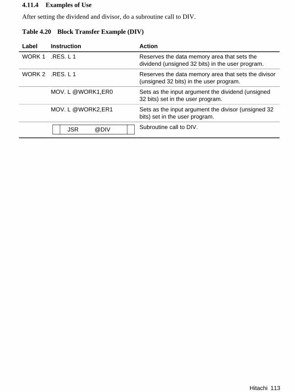
Hitachi 113
4.11.4 Examples of Use
After setting the dividend and divisor, do a subroutine call to DIV.
Table 4.20 Block Transfer Example (DIV)
Label Instruction Action
WORK 1 .RES. L 1 Reserves the data memory area that sets thedividend (unsigned 32 bits) in the user program.
WORK 2 .RES. L 1 Reserves the data memory area that sets the divisor(unsigned 32 bits) in the user program.
MOV. L @WORK1,ER0 Sets as the input argument the dividend (unsigned32 bits) set in the user program.
MOV. L @WORK2,ER1 Sets as the input argument the divisor (unsigned 32bits) set in the user program.
@DIVJSR Subroutine call to DIV.
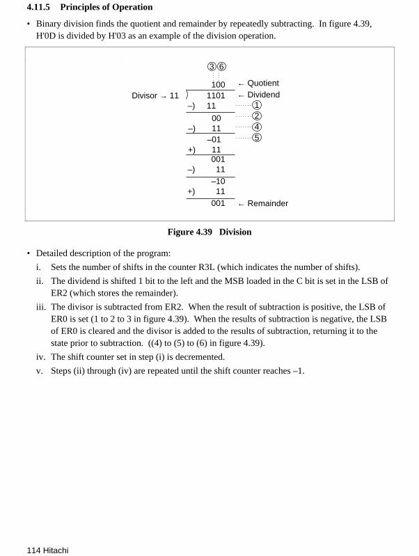
114 Hitachi
4.11.5 Principles of Operation
• Binary division finds the quotient and remainder by repeatedly subtracting. In figure 4.39,H'0D is divided by H'03 as an example of the division operation.
1001101
–) 11 Divisor → 11
00–) 11
–01+) 11
3 6
← Quotient← Dividend
1245
← Remainder
001–) 11
–10+) 11
001
Figure 4.39 Division
• Detailed description of the program:
i. Sets the number of shifts in the counter R3L (which indicates the number of shifts).
ii. The dividend is shifted 1 bit to the left and the MSB loaded in the C bit is set in the LSB ofER2 (which stores the remainder).
iii. The divisor is subtracted from ER2. When the result of subtraction is positive, the LSB ofER0 is set (1 to 2 to 3 in figure 4.39). When the results of subtraction is negative, the LSBof ER0 is cleared and the divisor is added to the results of subtraction, returning it to thestate prior to subtraction. ((4) to (5) to (6) in figure 4.39).
iv. The shift counter set in step (i) is decremented.
v. Steps (ii) through (iv) are repeated until the shift counter reaches –1.
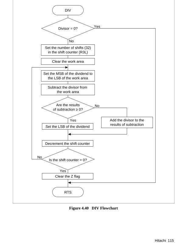
Hitachi 115
No
Yes
Is the shift counter = 0?
RTS
Add the divisor to theresults of subtraction
Yes
No
Divisor = 0?
DIV
Set the number of shifts (32)in the shift counter (R3L)
Clear the work area
Set the MSB of the dividend tothe LSB of the work area
Subtract the divisor from the work area
Set the LSB of the dividend
Are the resultsof subtraction ≥ 0?
Decrement the shift counter
Clear the Z flag
No
Yes
Figure 4.40 DIV Flowchart
116 Hitachi
4.11.6 Program Listing

Hitachi 117
4.12 Signed 16-Bit Binary Multiplication
MCU: H8/300H Series
Label Name: MULXS
Functions Used: MULXS.W Instruction
Function: Does multiplication in the format: Multiplicand (signed 16 bits) × multiplier (signed 16bits) = product (signed 32 bits).
Table 4.21 MULXS Arguments
Contents Storage Location Data Length (Bytes)
Input Multiplicand (signed 16 bits) R0 2
Multiplier (signed 16 bits) E0 2
Output Product (signed 32 bits) ER0 4
ER0
ER1
ER2
ER3
ER4
ER5
ER6
ER7(SP)
31 1516 78 0
I U H U N Z V C— — —
Product
↔ ↔— — —
—
↔
01
: No change: Changes: Locked to 0: Locked to 1
Multiplier Multiplicand
Figure 4.41 Changes in Internal Registers and Flag Changes for MULXS

118 Hitachi
4
0
0
24
Program memory (bytes)
Data memory (bytes)
Stack (bytes)
Number of states
Re-entrant
Yes
Relocation
Yes
Interrupts during execution
Yes
Figure 4.42 Programming Specifications

Hitachi 119
4.12.1 Description of Functions
Arguments are as follows:
• E0: Sets the multiplicand (signed 16 bits) as an input argument.
• R0: Sets the multiplier (signed 16 bits) as an input argument.
• ER0: Sets the product (signed 32 bits) as an output argument.
Figure 4.43 is an example of execution of the software MULXS.B When the input arguments areset as shown, the results of multiplication are set in ER0.
E0FFFF
R0FFFF
ER00000 1000
×)
Outputarguments
Inputarguments
Figure 4.43 Executing MULXS
4.12.2 Cautions for Use
Since the results of multiplication are set in the register used to set the multiplicand and multiplier,the multiplicand and multiplier are destroyed after MULXS is executed. When you will stillrequire the multiplicand and multiplier after executing MULXS, save them elsewhere in memorybeforehand.
4.12.3 Description of Data Memory
No data memory is used by MULXS.
120 Hitachi
4.12.4 Examples of Use
After setting the multiplicand and multiplier, do a subroutine call to MULXS.
Table 4.22 Block Transfer Example (MULXS)
Label Instruction Action
WORK 1 RES. W 1 Reserves the data memory area that sets themultiplicand (signed 16 bits) in the user program.
WORK 2 RES. W 1 Reserves the data memory area that sets themultiplier (signed 16 bits) in the user program.
MOV. L @WORK1,R0 Sets as the input argument the 16-bit binarymultiplicand set in the user program.
MOV. L @WORK2,E0 Sets as the input argument the 16-bit binarymultiplier set in the user program.
@MULXSJSR Subroutine call to MULXS.
4.12.5 Principles of Operation
Use the signed 16-bit multiplication instruction MULXS.W.
MULXS
Multiplication by the signed 16-bitmultiplication instruction MULXS.W
RTS
Figure 4.44 MULXS Flowchart

Hitachi 121
4.12.6 Program Listing
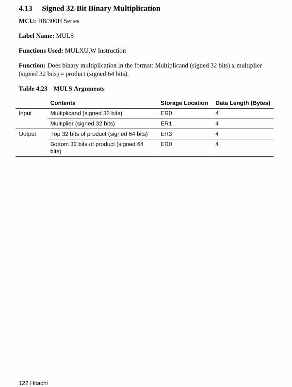
122 Hitachi
4.13 Signed 32-Bit Binary Multiplication
MCU: H8/300H Series
Label Name: MULS
Functions Used: MULXU.W Instruction
Function: Does binary multiplication in the format: Multiplicand (signed 32 bits) x multiplier(signed 32 bits) = product (signed 64 bits).
Table 4.23 MULS Arguments
Contents Storage Location Data Length (Bytes)
Input Multiplicand (signed 32 bits) ER0 4
Multiplier (signed 32 bits) ER1 4
Output Top 32 bits of product (signed 64 bits) ER3 4
Bottom 32 bits of product (signed 64bits)
ER0 4
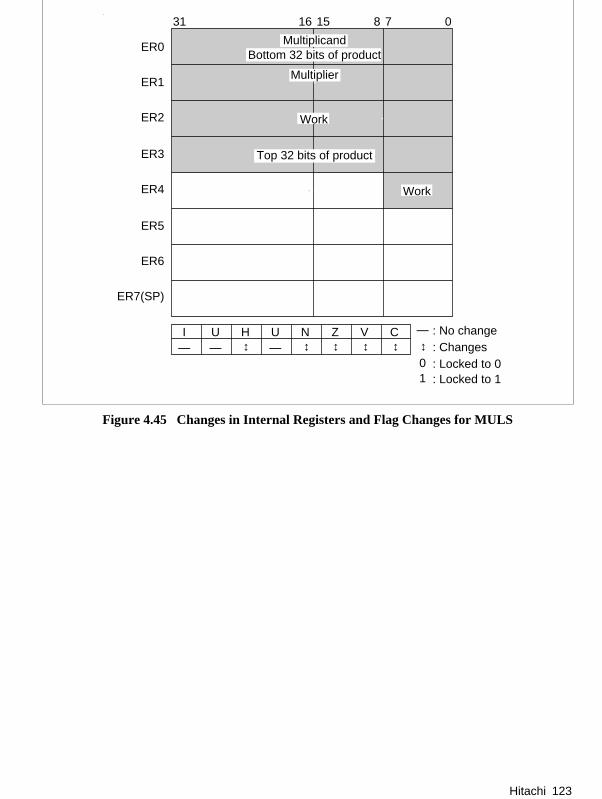
Hitachi 123
ER0
ER1
ER2
ER3
ER4
ER5
ER6
ER7(SP)
31 1516 78 0
I U H U N Z V C— — —
Top 32 bits of product
Work
↔ ↔ ↔ ↔
Work
↔
—
↔
01
: No change: Changes: Locked to 0: Locked to 1
Multiplier
MultiplicandBottom 32 bits of product
Figure 4.45 Changes in Internal Registers and Flag Changes for MULS
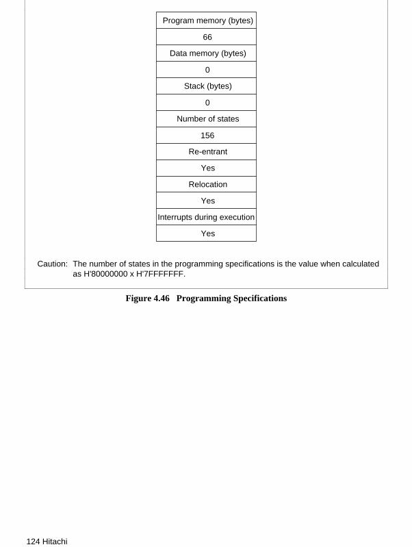
124 Hitachi
66
0
0
156
Program memory (bytes)
Data memory (bytes)
Stack (bytes)
Number of states
Re-entrant
Yes
Relocation
Yes
Interrupts during execution
Yes
Caution: The number of states in the programming specifications is the value when calculatedas H'80000000 x H'7FFFFFFF.
Figure 4.46 Programming Specifications

Hitachi 125
4.13.1 Description of Functions
Arguments are as follows:
• ER0: Sets the multiplicand (signed 32 bits) as an input argument. Sets the bottom 32 bits of theproduct (signed 64 bits) as an output argument.
• ER1: Sets the multiplier (signed 32 bits) as an input argument. Sets the bottom 32 bits of theproduct (signed 64 bits) as an output argument.
• Sets the top 32 bits of the product (signed 64 bits) as an output argument.
Figure 4.47 is an example of execution of the software MULS. When the input arguments are setas shown, the product is set in ER3 and ER0.
ER0FFF7 FFFF
ER10008 0000
00000CER0000800 0000
ER3
×)
Outputarguments
Inputarguments
Figure 4.47 Executing MULS
4.13.2 Cautions for Use
Since the results of multiplication are set in the register used to set the multiplicand and multiplier,the multiplicand and multiplier are destroyed after MULS is executed. When you will still requirethe multiplicand and multiplier after executing MULS, save them elsewhere in memorybeforehand.
4.13.3 Description of Data Memory
No data memory is used by MULS.
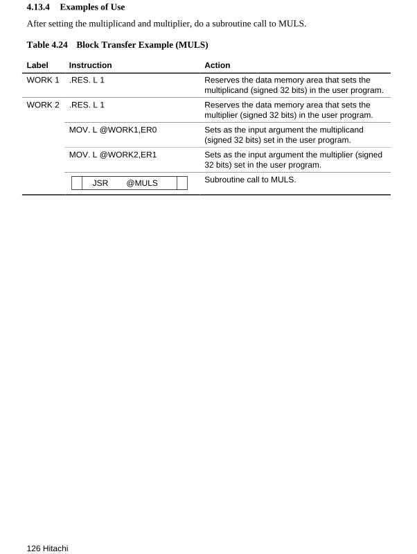
126 Hitachi
4.13.4 Examples of Use
After setting the multiplicand and multiplier, do a subroutine call to MULS.
Table 4.24 Block Transfer Example (MULS)
Label Instruction Action
WORK 1 .RES. L 1 Reserves the data memory area that sets themultiplicand (signed 32 bits) in the user program.
WORK 2 .RES. L 1 Reserves the data memory area that sets themultiplier (signed 32 bits) in the user program.
MOV. L @WORK1,ER0 Sets as the input argument the multiplicand(signed 32 bits) set in the user program.
MOV. L @WORK2,ER1 Sets as the input argument the multiplier (signed32 bits) set in the user program.
@MULSJSR Subroutine call to MULS.

Hitachi 127
4.13.5 Principles of Operation
• Negative multiplicands and multipliers are converted to positive.
• The product is found by taking the partial products ((1), (2), (3) and (4) in figure 4.48) and thenaccumulating the results of multiplication (figure 4.48 (5)). The partial products are found byusing the signed multiplication instruction (MULXU.W) on two 16-bit binary numbers.
• The product is then converted to negative if the sign flag is 1, as shown in table 4.25.
Bottom 16 bits of multiplicand
R0E0
ER0
×)
...Partial product (1)
ER0ER3
Top 16 bits of multiplicand
Bottom 16 bits of multiplier
R1E1Top 16 bits of multiplier
Bottom 16 bits of multiplicand ×bottom 16 bits of multiplier
ER1...Partial product (2)
Top 16 bits of multiplicand ×bottom 16 bits of multiplier
ER2...Partial product (3)
Bottom 16 bits of multiplicand ×top 16 bits of multiplier
ER3...Partial product (4)
Top 16 bits of multiplicand ×top 16 bits of multiplier
...Results of multiplication (5)
Figure 4.48 Multiplication
Table 4.25 Sign of Results of Multiplication and Sign Flag
Multiplicand Multiplier Product Sign Flag
Positive Positive Positive 0
Negative Negative 1
Negative Positive Negative 1
Negative Positive 0

128 Hitachi
1
No
Yes
Is multiplicand ≥ 0?
MULS
Bottom 16 bits of mutiplicand× bottom 16 bits of multiplier:
Partial product 1
Multiplicand convertedto positive
Clear sign flag
Sign flag inverted
No
Yes
Is multiplier ≥ 0?
Multiplier convertedto positive
Sign flag inverted
Top 16 bits of mutiplicand× bottom 16 bits of multiplier:
Partial product 2
Bottom 16 bits of mutiplicand× top 16 bits of multiplier:
Partial product 3
Top 16 bits of mutiplicand× top 16 bits of multiplier:
Partial product 4
Figure 4.49 MULS Flowchart

Hitachi 129
1
Yes
No
Is C flag = 1?
Partial product 2 + partial product 3
Increment register E3
Top 16 bits of partial product 1+ bottom 16 bits of (partial
product 2 + partial product 3)
Yes
No
Is C flag = 1?
Increment register ER3
Bottom 16 bits of partialproduct 4 + top 16 bits of (partial
product 2 + partial product 3)
Yes
No
Is C flag = 1?
Increment register E3
2
Figure 4.49 MULS Flowchart (cont)
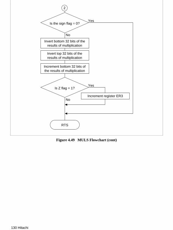
130 Hitachi
Yes
No
Is the sign flag = 0?
Invert bottom 32 bits of theresults of multiplication
Yes
No
Is Z flag = 1?
Increment register ER3
RTS
Invert top 32 bits of theresults of multiplication
Increment bottom 32 bits ofthe results of multiplication
2
Figure 4.49 MULS Flowchart (cont)

Hitachi 131
4.13.6 Program Listing

132 Hitachi
4.14 Signed 32-Bit Binary Division (16-Bit Divisor)
MCU: H8/300H Series
Label Name: DIVXS
Functions Used: DIVXS.W Instruction
Function: Does division in the format: Dividend (signed 32 bits) / divisor (signed 16 bits) =quotient (signed 32 bits) … remainder (signed 16 bits).
Table 4.26 DIVXS Arguments
Contents Storage Location Data Length (Bytes)
Input Dividend (signed 32 bits) ER1 4
Divisor (signed 16 bits) R0 2
Output Quotient (signed 32 bits) ER2 4
Remainder (signed 16 bits) E1 2
Presence of error Z flag (CCR) 1
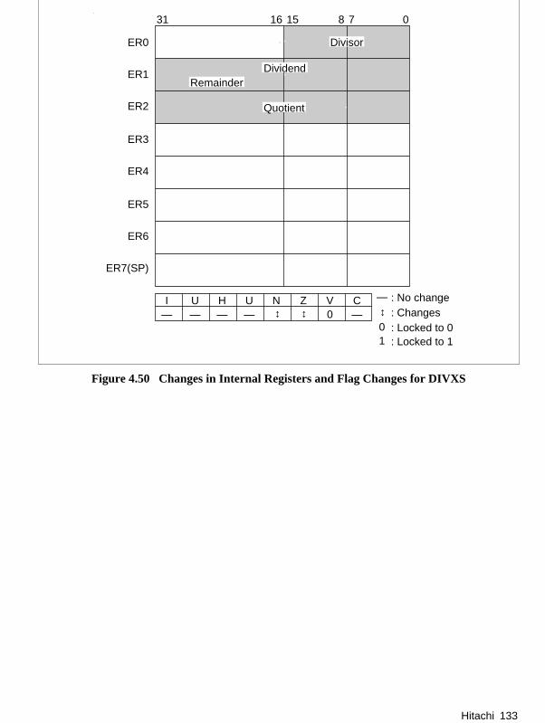
Hitachi 133
ER0
ER1
ER2
ER3
ER4
ER5
ER6
ER7(SP)
31 1516 78 0
I U H U N Z V C— — —
Divisor
Dividend
Quotient
↔ ↔— 0
—
↔
01
: No change: Changes: Locked to 0: Locked to 1
Remainder
—
Figure 4.50 Changes in Internal Registers and Flag Changes for DIVXS
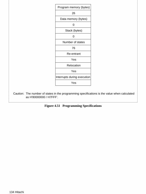
134 Hitachi
26
0
0
76
Program memory (bytes)
Data memory (bytes)
Stack (bytes)
Number of states
Re-entrant
Yes
Relocation
Yes
Interrupts during execution
Yes
Caution: The number of states in the programming specifications is the value when calculatedas H'80000000 / H7FFF'.
Figure 4.51 Programming Specifications

Hitachi 135
4.14.1 Description of Functions
Arguments are as follows
• R0: Sets the divisor (signed 16 bits) as an input argument.
• ER1: Sets the dividend (signed 32 bits) as an input argument.
• ER2: Sets the quotient (signed 32 bits) as an output argument.
• E1: Sets the remainder (signed 16 bits) as an output argument.
• Z Flag (CCR): Indicates whether there are any errors (division by 0) after execution of DIVXS.
— When Z flag = 1: Indicates that there is an error in the division.
— When Z flag = 0: Indicates that there is no error in the division.
Figure 4.52 is an example of execution of the software DIVXS. When the input arguments are setas shown, the quotient is set in ER2 and the remainder is set in ER1.
E10000
ER2FFFF FFFF
FFFF FFFF
R0
789A
Input arguments
Output arguments
0Z flag
ER1
Figure 4.52 Executing DIVXS
• With the software DIVXS, the first thing done is to determine if the divisor is 0 or nonzero; if itis 0, DIVXS ends.
4.14.2 Cautions for Use
Since the remainder is set in E1 and the bottom 16 bits of the quotient are set in R1, the dividendis destroyed after DIVXS is executed. When you will still require the dividend after executingDIVXS, save it elsewhere in memory beforehand.
4.14.3 Description of Data Memory
No data memory is used by DIVXS.
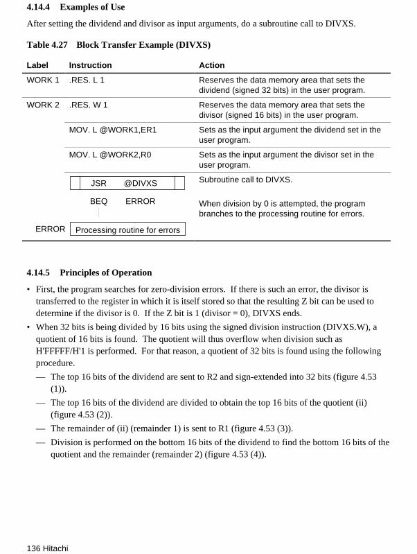
136 Hitachi
4.14.4 Examples of Use
After setting the dividend and divisor as input arguments, do a subroutine call to DIVXS.
Table 4.27 Block Transfer Example (DIVXS)
Label Instruction Action
WORK 1 .RES. L 1 Reserves the data memory area that sets thedividend (signed 32 bits) in the user program.
WORK 2 .RES. W 1 Reserves the data memory area that sets thedivisor (signed 16 bits) in the user program.
MOV. L @WORK1,ER1 Sets as the input argument the dividend set in theuser program.
MOV. L @WORK2,R0 Sets as the input argument the divisor set in theuser program.
@DIVXSJSR
ERRORBEQ
Processing routine for errorsERROR
Subroutine call to DIVXS.
When division by 0 is attempted, the programbranches to the processing routine for errors.
4.14.5 Principles of Operation
• First, the program searches for zero-division errors. If there is such an error, the divisor istransferred to the register in which it is itself stored so that the resulting Z bit can be used todetermine if the divisor is 0. If the Z bit is 1 (divisor = 0), DIVXS ends.
• When 32 bits is being divided by 16 bits using the signed division instruction (DIVXS.W), aquotient of 16 bits is found. The quotient will thus overflow when division such asH'FFFFF/H'1 is performed. For that reason, a quotient of 32 bits is found using the followingprocedure.
— The top 16 bits of the dividend are sent to R2 and sign-extended into 32 bits (figure 4.53(1)).
— The top 16 bits of the dividend are divided to obtain the top 16 bits of the quotient (ii)(figure 4.53 (2)).
— The remainder of (ii) (remainder 1) is sent to R1 (figure 4.53 (3)).
— Division is performed on the bottom 16 bits of the dividend to find the bottom 16 bits of thequotient and the remainder (remainder 2) (figure 4.53 (4)).
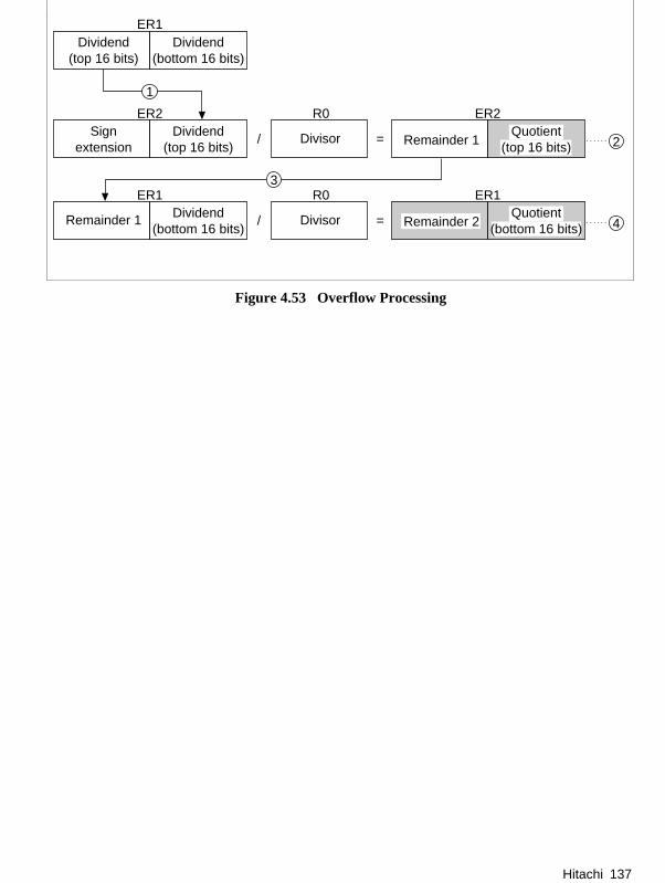
Hitachi 137
Dividend(top 16 bits)
ER1
1
/ =
3
2
ER2
Dividend(bottom 16 bits)
Signextension
Dividend(top 16 bits)
R0
Divisor
ER2
Remainder 1Quotient
(top 16 bits)
/ = 4
ER1
Remainder 1 Dividend(bottom 16 bits)
R0
Divisor
ER1Quotient
(bottom 16 bits)Remainder 2
Figure 4.53 Overflow Processing

138 Hitachi
Yes
No
Is divisor = 0?(Z bit = 1)
Sign-extend the top 16 bits ofthe dividend to 32 bits
RTS
Divide the top 16 bits of thedividend that was extended to
32 bits (ER2) by the divisor (R0)
DIVXS
Divide the bottom 16 bits (ER1)of the dividend, whose top 16
bits are the remainder (E2)from the division of the top 16
bits of the dividend(ER2), by the divisor (R0)
Set the top 16 bits of thequotient (R2) as an output
argument (E2)
Set the bottom 16 bits of thequotient (R1) as an output
argument (R2)
Clear the Z flag
Figure 4.54 DIVXS Flowchart

Hitachi 139
4.14.6 Program Listing

140 Hitachi
4.15 Signed 32-Bit Binary Division (32-Bit Divisor)
MCU: H8/300H Series
Label Name: DIVS
Functions Used: SHLL.L Instruction, ROTL.L Instruction, NEG.L Instruction
Function: Does division in the format: Dividend (signed 32 bits) / divisor (signed 32 bits) =quotient (signed 32 bits) … remainder (signed 32 bits).
Table 4.28 DIVS Arguments
Contents Storage Location Data Length (Bytes)
Input Dividend (signed 32 bits) ER0 4
Divisor (signed 32 bits) ER1 4
Output Quotient (signed 32 bits) ER0 4
Remainder (signed 32 bits) ER2 4
Presence of error Z flag (CCR) 1

Hitachi 141
ER0
ER1
ER2
ER3
ER4
ER5
ER6
ER7(SP)
31 1516 78 0
I U H U N Z V C— — —
Dividend
Divisor
Remainder
↔ ↔ ↔ ↔
Work
↔
Work
—
↔
01
: No change: Changes: Locked to 0: Locked to 1
Quotient
Figure 4.55 Changes in Internal Registers and Flag Changes for DIVS

142 Hitachi
66
0
0
770
Program memory (bytes)
Data memory (bytes)
Stack (bytes)
Number of states
Re-entrant
Yes
Relocation
Yes
Interrupts during execution
Yes
Caution: The number of states in the programming specifications is the value when calculatedas H'80000000 / H7FFFFFFF.
Figure 4.56 Programming Specifications
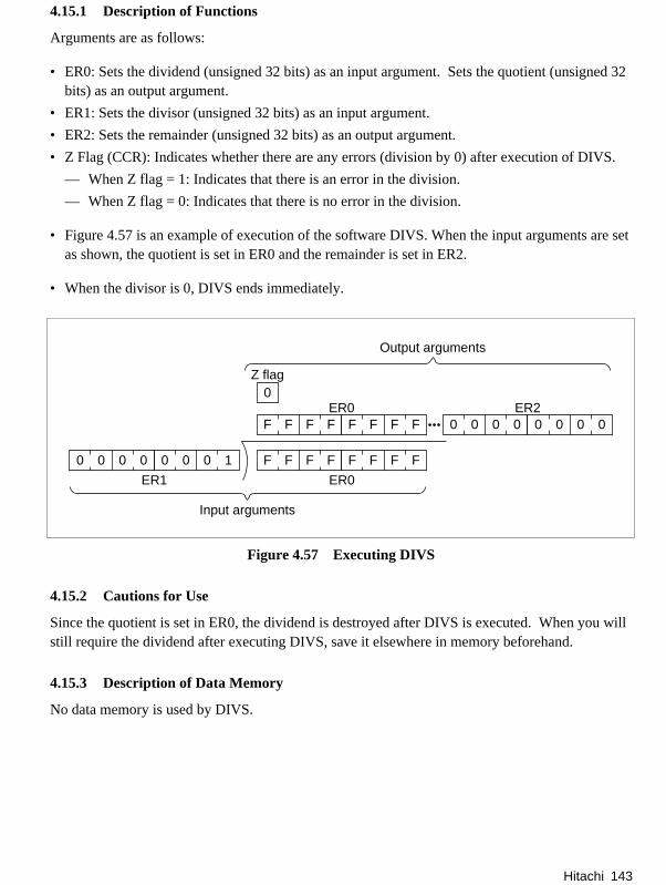
Hitachi 143
4.15.1 Description of Functions
Arguments are as follows:
• ER0: Sets the dividend (unsigned 32 bits) as an input argument. Sets the quotient (unsigned 32bits) as an output argument.
• ER1: Sets the divisor (unsigned 32 bits) as an input argument.
• ER2: Sets the remainder (unsigned 32 bits) as an output argument.
• Z Flag (CCR): Indicates whether there are any errors (division by 0) after execution of DIVS.
— When Z flag = 1: Indicates that there is an error in the division.
— When Z flag = 0: Indicates that there is no error in the division.
• Figure 4.57 is an example of execution of the software DIVS. When the input arguments are setas shown, the quotient is set in ER0 and the remainder is set in ER2.
• When the divisor is 0, DIVS ends immediately.
ER20000 0000
ER0FFFF FFFF
FFFF FFFF
ER1
0000 1000
Input arguments
Output arguments
0Z flag
ER0
Figure 4.57 Executing DIVS
4.15.2 Cautions for Use
Since the quotient is set in ER0, the dividend is destroyed after DIVS is executed. When you willstill require the dividend after executing DIVS, save it elsewhere in memory beforehand.
4.15.3 Description of Data Memory
No data memory is used by DIVS.

144 Hitachi
4.15.4 Examples of Use
After setting the dividend and divisor, do a subroutine call to DIVS.
Table 4.29 Block Transfer Example (DIVS)
Label Instruction Action
WORK 1 .RES. L 1 Reserves the data memory area that sets thedividend (signed 32 bits) in the user program.
WORK 2 .RES. L 1 Reserves the data memory area that sets the divisor(signed 32 bits) in the user program.
MOV. L @WORK1,ER0 Sets as the input argument the dividend (signed 32bits) set in the user program.
MOV. L @WORK2,ER1 Sets as the input argument the divisor (signed 32bits) set in the user program.
@DIVSJSR Subroutine call to DIVS.

Hitachi 145
4.15.5 Principles of Operation
• Negative dividends and divisors are converted to positive.
• Division finds the quotient and remainder by repeatedly subtracting. In figure 4.58, H'0D isdivided by H'03 as an example of the division operation.
i. Sets the number of shifts in the counter R3L (which indicates the number of shifts).
ii. The dividend is shifted 1 bit to the left and the MSB loaded in the C bit is set in the LSB ofER2 (which stores the remainder).
iii. The divisor is subtracted from ER2. When the result of subtraction is positive, the LSB ofER0 is set. ((1) to (2) to (3) in figure 4.58). When the results of subtraction is negative, theLSB of ER0 is cleared and the divisor is added to the results of subtraction, returning it tothe state prior to subtraction. ((4) to (5) to (6) in figure 4.58).
iv. The shift counter set in step (i) is decremented.
v. Steps (ii) through (iv) are repeated until the shift counter reaches -1.
• The quotient and/or remainder is then converted to negative if the sign flag is 1, as shown intable 4.30.
1001101
–) 11 Divisor → 11
00–) 11
–01+) 11
3 6
← Quotient← Dividend
1245
← Remainder
001–) 11
–10+) 11
001
Figure 4.58 Division Example
Table 4.30 Sign of Results of Division and the Sign Flag
Dividend Divisor Quotient Remainder Quotient Sign Flag Remainder Sign Flag
Positive Positive Positive Positive 0 0
Negative Negative Positive 1 0
Negative Positive Negative Negative 1 1
Negative Positive Positive 0 0

146 Hitachi
4.15.6 Program Listing

Hitachi 147
4.16 8-Digit Decimal Addition
MCU: H8/300H Series
Label Name: ADDD
Functions Used: DAA.B Instruction
Function: Does addition in the format: Summand (8-digit 4-bit BCD) × addend (8-digit 4-bitBCD) = sum (8-digit 4-bit BCD).
Table 4.31 ADDD Arguments
Contents Storage Location Data Length (Bytes)
Input Summand (8-digit 4-bit BCD) ER0 4
Summand (8-digit 4-bit BCD) ER1 4
Output Sum (8-digit 4-bit BCD) ER0 4
Presence of carry (Yes, C = 1;No, C = 0)
C flag 1

148 Hitachi
ER0
ER1
ER2
ER3
ER4
ER5
ER6
ER7(SP)
31 1516 78 0
I U H U N Z V C— — —
Summand (8-digit 4-bit BCD)
Addend (8-digit 4-bit BCD)
↔ ↔ ↔ ↔0
—
↔
01
: No change: Changes: Locked to 0: Locked to 1
Sum (8-digit 4-bit BCD)
Figure 4.59 Changes in Internal Registers and Flag Changes for DIVS

Hitachi 149
28
0
0
36
Program memory (bytes)
Data memory (bytes)
Stack (bytes)
Number of states
Re-entrant
Yes
Relocation
Yes
Interrupts during execution
Yes
Figure 4.60 Programming Specifications
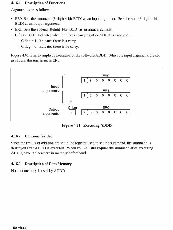
150 Hitachi
4.16.1 Description of Functions
Arguments are as follows:
• ER0: Sets the summand (8-digit 4-bit BCD) as an input argument. Sets the sum (8-digit 4-bitBCD) as an output argument.
• ER1: Sets the addend (8-digit 4-bit BCD) as an input argument.
• C flag (CCR): Indicates whether there is carrying after ADDD is executed.
— C flag = 1: Indicates there is a carry.
— C flag = 0: Indicates there is no carry.
Figure 4.61 is an example of execution of the software ADDD. When the input arguments are setas shown, the sum is set in ER0.
ER00081 0000
ER10021 0000
C flag
+)
Outputarguments
Inputarguments
ER00000 00003
Figure 4.61 Executing ADDD
4.16.2 Cautions for Use
Since the results of addition are set in the register used to set the summand, the summand isdestroyed after ADDD is executed. When you will still require the summand after executingADDD, save it elsewhere in memory beforehand.
4.16.3 Description of Data Memory
No data memory is used by ADDD
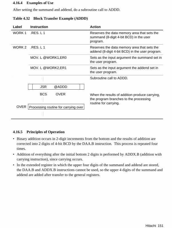
Hitachi 151
4.16.4 Examples of Use
After setting the summand and addend, do a subroutine call to ADDD.
Table 4.32 Block Transfer Example (ADDD)
Label Instruction Action
WORK 1 .RES. L 1 Reserves the data memory area that sets thesummand (8-digit 4-bit BCD) in the userprogram.
WORK 2 .RES. L 1 Reserves the data memory area that sets theaddend (8-digit 4-bit BCD) in the user program.
MOV. L @WORK1,ER0 Sets as the input argument the summand set inthe user program.
MOV. L @WORK2,ER1 Sets as the input argument the addend set inthe user program.
@ADDDJSR
OVERBCS
Processing routine for carrying overOVER
Subroutine call to ADDD.
When the results of addition produce carrying,the program branches to the processingroutine for carrying.
4.16.5 Principles of Operation
• Binary addition occurs in 2-digit increments from the bottom and the results of addition arecorrected into 2 digits of 4-bit BCD by the DAA.B instruction. This process is repeated fourtimes.
• Addition of everything after the initial bottom 2 digits is performed by ADDX.B (addition withcarrying instruction), since carrying occurs.
• In the extended register in which the upper four digits of the summand and addend are stored,the DAA.B and ADDX.B instructions cannot be used, so the upper 4 digits of the summand andaddend are added after transfer to the general registers.

152 Hitachi
RTS
Binary addition of firstand second digits
ADDD
Decimal correction ofresults of addition
Binary addition with carryof the third and fourth digits
Decimal correction ofresults of addition
Transfer the top 4 digitsof the addend (E1) to R1
Transfer the lower 4 digitsof results of addition
(R0) to E1
Transfer the top 4 digitsof the summand (E0) to R0
Binary addition with carryof the fifth and sixth digits
Decimal correction ofresults of addition
Binary addition with carryof the seventh and
eighth digits
Decimal correction ofresults of addition
Figure 4.62 ADDD Flowchart
Hitachi 153
4.16.6 Program Listing

Hitachi 155
4.17 8-Digit Decimal Subtraction
MCU: H8/300H Series
Label Name: SUBD
Functions Used: DAS.B Instruction
Function: Does subtraction in the format: Minuend (8-digit 4-bit BCD) – subtrahend (8-digit 4-bitBCD) = difference (8-digit 4-bit BCD).
Table 4.33 SUBD Arguments
Contents Storage Location Data Length (Bytes)
Input Minuend (8-digit 4-bit BCD) ER0 4
Subtrahend (8-digit 4-bit BCD) ER1 4
Output Difference (8-digit 4-bit BCD) ER0 4
Presence of borrow (Yes, C = 1; No, C = 0) C flag (CCR) 1
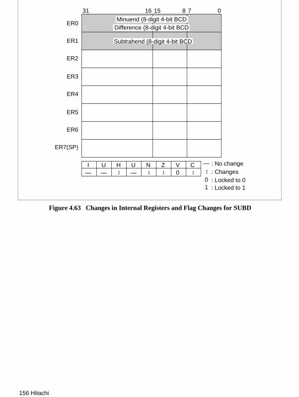
156 Hitachi
ER0
ER1
ER2
ER3
ER4
ER5
ER6
ER7(SP)
31 1516 78 0
I U H U N Z V C— — —
Minuend (8-digit 4-bit BCD
Subtrahend (8-digit 4-bit BCD
↔ ↔ ↔ ↔0
—
↔
01
: No change: Changes: Locked to 0: Locked to 1
Difference (8-digit 4-bit BCD
Figure 4.63 Changes in Internal Registers and Flag Changes for SUBD

Hitachi 157
28
0
0
36
Program memory (bytes)
Data memory (bytes)
Stack (bytes)
Number of states
Re-entrant
Yes
Relocation
Yes
Interrupts during execution
Yes
Figure 4.64 Programming Specifications

158 Hitachi
4.17.1 Description of Functions
Arguments are as follows:
• ER0: Sets the minuend (8-digit 4-bit BCD) as an input argument. Sets the difference (8-digit,4-bit BCD) as an output argument.
• ER1: Sets the subtrahend (8-digit 4-bit BCD) as an input argument.
• C flag (CCR): Indicates whether there is borrowing after SUBD is executed.
— C flag = 1: Indicates there is a borrow.
— C flag = 0: Indicates there is no borrow.
Figure 4.65 is an example of execution of the software SUBD. When the input arguments are setas shown, the difference is set in ER0.
ER00081 0000
ER10021 0000
C flag
–)
Outputarguments
Inputarguments
ER00060 00000
Figure 4.65 Executing SUBD
4.17.2 Cautions for Use
Since the results of subtraction are set in the register used to set the minuend, the minuend isdestroyed after SUBD is executed. When you will still require the minuend after executingSUBD, save it elsewhere in memory beforehand.
4.17.3 Description of Data Memory
No data memory is used by SUBD.

Hitachi 159
4.17.4 Examples of Use
After setting the minuend and subtrahend, do a subroutine call to SUBD.
Table 4.34 Block Transfer Example (SUBD)
Label Instruction Action
WORK 1 .RES. L 1 Reserves the data memory area that sets theminuend (8-digit 4-bit BCD) in the user program.
WORK 2 .RES. L 1 Reserves the data memory area that sets thesubtrahend (8-digit 4-bit BCD) in the userprogram.
MOV. L @WORK1,ER0 Sets as the input argument the minuend set inthe user program.
MOV. L @WORK2,ER1 Sets as the input argument the subtrahend set inthe user program.
@SUBDJSR
OVERBCS
Processing routine for borrowingOVER
Subroutine call to SUBD.
When the results of subtraction produceborrowing, the program branches to theprocessing routine for borrowing.
4.17.5 Principles of Operation
• Binary subtraction occurs in 2-digit increments from the bottom and the results of subtractionare corrected into 2 digits of 4-bit BCD by the DAS.B instruction. This process is repeated fourtimes.
• Subtraction of everything after the initial bottom 2 digits is performed by SUBX.B (subtractionwith borrowing instruction), since borrowing occurs.
• In the extended register in which the upper four digits of the minuend and subtrahend are stored,the DAS.B and SUBX.B instructions cannot be used, so the upper 4 digits of the minuend andsubtrahend are subtracted after transfer to the general registers.

160 Hitachi
RTS
Binary subtraction of firstand second digits
SUBD
Decimal correction ofresults of subtraction
Binary subtraction with borrowof the third and fourth digits
Decimal correction ofresults of subtraction
Transfer the top 4 digitsof the subtrahend (E1) to R1
Transfer the lower 4 digitsof results of subtraction
(R0) to E1
Transfer the top 4 digitsof the minuend (E0) to R0
Binary subtraction with borrowof the fifth and sixth digits
Decimal correction ofresults of subtraction
Binary subtraction withborrow of the seventh and
eighth digits
Decimal correction ofresults of subtraction
Figure 4.66 SUBD Flowchart
Hitachi 161
4.17.6 Program Listing

162 Hitachi
4.18 Sum of Products
MCU: H8/300H Series
Label Name: SEKIWA
Functions Used: MULXU.W Instruction
Function: Does the following sum of products on unsigned 16-bit data an, bn (n = 1, 2, …, n)from data tables a and b. The maximum number of data n is 255.
a n bn = a1b1 + a2b2 + ... + anbn
n = 1
n∑
Table 4.35 SEKIWA Arguments
Contents Storage Location Data Length (Bytes)
Input Start address of data table a ER0 4
Start address of data table b ER1 4
Number of data n R3H 1
Output Results of sum of products (top8 bits)
R3L 1
Results of sum of products(bottom 32 bits)
ER2 4
Hitachi 163
ER0
ER1
ER2
ER3
ER4
ER5
ER6
ER7(SP)
31 1516 78 0
I U H U N Z V C— — —
Start address of data table a
Start address of data table b
↔ ↔ ↔ ↔1
Results of sum of products (bottom 32 bits)
Work
—
↔
01
: No change: Changes: Locked to 0: Locked to 1
Results of sumof products(top 8 bits)
Number ofdata n
Figure 4.67 Changes in Internal Registers and Flag Changes for SUBD

164 Hitachi
20
0
0
11234
Program memory (bytes)
Data memory (bytes)
Stack (bytes)
Number of states
Re-entrant
Yes
Relocation
Yes
Interrupts during execution
Yes
Caution: The number of states in the programming specifications is the value when the numberof data n is H'FF.
Figure 4.68 Programming Specifications
Hitachi 165
4.18.1 Description of Functions
Arguments are as follows:
• ER0: Sets the start address of data table a (multiplicands) as an input argument.
• ER1: Sets the start address of data table b (multipliers) as an input argument.
• R3H: Sets the number as an input argument.
• R3L: Sets the top 8 bits of the result of the sum of products operation as an output argument.
• ER2: Sets the bottom 32 bits of the result of the sum of products operation as an outputargument.
Figure 4.69 is an example of execution of the software. When the start address of data table a, startaddress of data table b, and number are set as shown, the top 8 bits of the result of the sum ofproducts operation are set in R3L and bottom 32 bits of the result of the sum of products operationare set in ER2.
FFFF1000
800000
Inputargurments
Don't care
ER0000008
Don't care
ER100000F
R3H30
C6AA
Data table a
FFFFCDFF9B70
F00000
Data a1
Data a2
Data a3
Data b1
Data b2
Data b3
Data table b
Output arguments
5810 8CD7 16 Σ anbn = a1b1 + a2b2 + a3b3 =
R3L ER23
n = 1
Figure 4.69 Executing SEKIWA
4.18.2 Cautions for Use
Since R0H is 1 byte, set data in the range H'01 ≤ R3H ≤ H'FF.

166 Hitachi
4.18.3 Description of Data Memory
No data memory is used by SEKIWA.
4.18.4 Examples of Use
After setting the start address of data table a, start address of data table b and number, do asubroutine call to SEKIWA.
Table 4.36 Block Transfer Example (SEKIWA)
Label Instruction Action
WORK 1 .RES. L 1 Reserves the data memory area that sets the startaddress of data table a in the user program.
WORK 2 .RES. L 1 Reserves the data memory area that sets the startaddress of data table b in the user program.
WORK 3 .RES. B 1 Reserves the data memory area that sets thenumber in the user program.
MOV. L @WORK1,ER0 Sets as the input argument the start address of datatable a set in the user program.
MOV. L @WORK2,ER1 Sets as the input argument the start address of datatable b set in the user program.
MOV. B @WORK3,R3H Sets as the input argument the number set in theuser program
@SEKIWAJSR
Subroutine call to SEKIWA.
4.18.5 Principles of Operation
1. ER0 and ER1 are used as pointers to the addresses of the multiplicand (data table a) andmultiplier (data table b) data. After the multiplicands and multipliers are set in E4 and R4respectively, the program increments to the next data address by post-increment registerindirect.
2. E4 and R4 are de-signed and multiplied.
3. The results of multiplication stored in ER4 are added to ER2, where the bottom 32 bits of theresults of the sum of products are stored.
4. Because of carrying, addition of R3L, where the top 8 bits of the result of the sum of productsis stored, uses addition with carrying.
5. R3H is decremented and the processes of steps 1 through 4 repeat until R3H = –1.

Hitachi 167
Yes
No
RTS
Is the itemnumber (R3H) = –1?
Data an (@ER0) of data table ais set in the multiplier register (E4)
SEKIWA
Data bn (@ER1) of data table bis set in the multiplier register (R4)
Increment to the address of the next data an + 1 of data table a
Increment to the address of the next data bn + 1 of data table b
Multiply
Add the results of multiplication(ER4) to the lower 32 bits of the
result of the sum of products (ER2)
Add the C bit to the top 8 bitsof the results of the sum of
products (R3L)
Decrement the item number (R3H)
Figure 4.70 SEKIWA Flowchart

168 Hitachi
4.18.6 Program Listing
Hitachi 169
4.19 Sorting
MCU: H8/300H Series
Label Name: SORT
Functions Used: Post-Increment Register Indirect, Pre-Decrement Register Indirect
Function: Sorts data (unsigned 16 bits) of the data table from largest to smallest. The maximumnumber of data is 65535.
Table 4.37 SORT Arguments
Contents Storage Location Data Length (Bytes)
Input Number of sort data R0 2
Start address of data table ER2 4
Output — — —
ER0
ER1
ER2
ER3
ER4
ER5
ER6
ER7(SP)
31 1516 78 0
I U H U N Z V C— — — 0
Work
Start address of data table
Work Number of sort data
Work Work
0100
—
↔
01
: No change: Changes: Locked to 0: Locked to 1
Figure 4.71 Changes in Internal Registers and Flag Changes for SORT
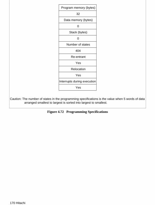
170 Hitachi
32
0
0
404
Program memory (bytes)
Data memory (bytes)
Stack (bytes)
Number of states
Re-entrant
Yes
Relocation
Yes
Interrupts during execution
Yes
Caution: The number of states in the programming specifications is the value when 5 words of dataarranged smallest to largest is sorted into largest to smallest.
Figure 4.72 Programming Specifications
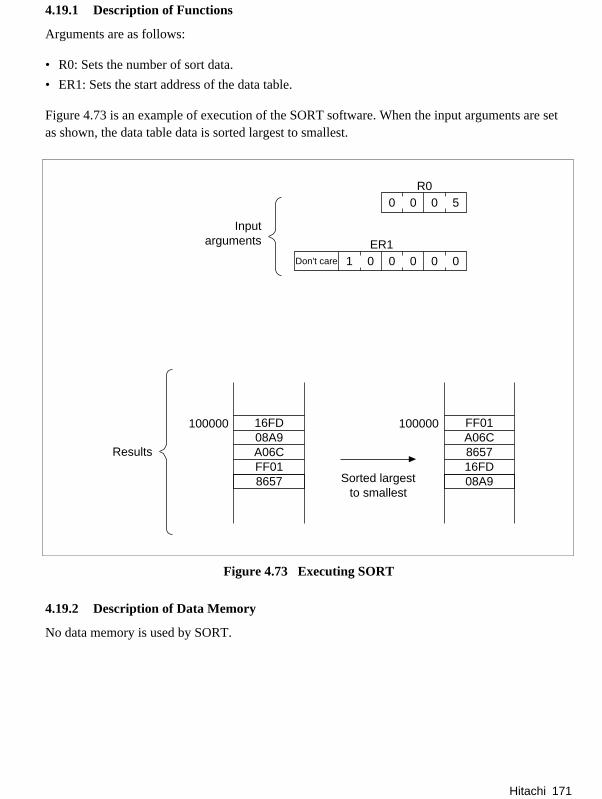
Hitachi 171
4.19.1 Description of Functions
Arguments are as follows:
• R0: Sets the number of sort data.
• ER1: Sets the start address of the data table.
Figure 4.73 is an example of execution of the SORT software. When the input arguments are setas shown, the data table data is sorted largest to smallest.
16FD08A9A06CFF01
100000
8657
R05000
Inputarguments
FF01A06C865716FD
100000
08A9
Results
Sorted largestto smallest
Don't care
ER1000001
Figure 4.73 Executing SORT
4.19.2 Description of Data Memory
No data memory is used by SORT.

172 Hitachi
4.19.3 Examples of Use
After setting the start address of the data table and the number of sort data, do a subroutine call toSORT.
Table 4.38 Block Transfer Example (SORT)
Label Instruction Action
WORK 1 .RES. W 1 Reserves the data memory area that sets thenumber of sort data in the user program.
WORK 2 .RES. L 1 Reserves the data memory area that sets the startaddress of the data table in the user program.
MOV. W @WORK1,R0 Sets as the input argument the number of sort dataset in the user program.
MOV. L @WORK2,ER1 Sets as the input argument the start address of thedata table set in the user program.
@SORTJSR
Subroutine call of SORT.
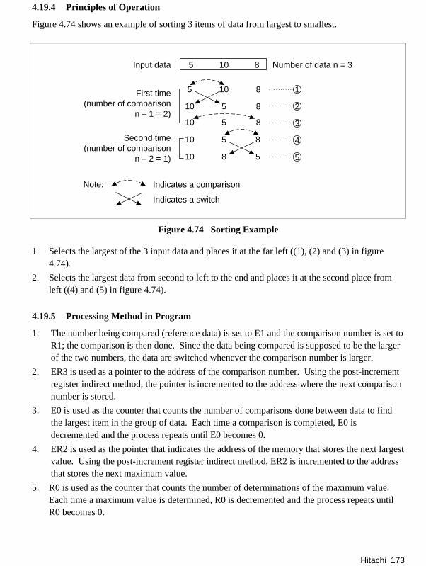
Hitachi 173
4.19.4 Principles of Operation
Figure 4.74 shows an example of sorting 3 items of data from largest to smallest.
5 10 8Input data
First time(number of comparison
n – 1 = 2)
Second time(number of comparison
n – 2 = 1)
5 10
10 5
10 5 8
10 5
10 8
8
5
8
8 1
2
3
4
5
Number of data n = 3
Indicates a comparison
Indicates a switch
Note:
Figure 4.74 Sorting Example
1. Selects the largest of the 3 input data and places it at the far left ((1), (2) and (3) in figure4.74).
2. Selects the largest data from second to left to the end and places it at the second place fromleft ((4) and (5) in figure 4.74).
4.19.5 Processing Method in Program
1. The number being compared (reference data) is set to E1 and the comparison number is set toR1; the comparison is then done. Since the data being compared is supposed to be the largerof the two numbers, the data are switched whenever the comparison number is larger.
2. ER3 is used as a pointer to the address of the comparison number. Using the post-incrementregister indirect method, the pointer is incremented to the address where the next comparisonnumber is stored.
3. E0 is used as the counter that counts the number of comparisons done between data to findthe largest item in the group of data. Each time a comparison is completed, E0 isdecremented and the process repeats until E0 becomes 0.
4. ER2 is used as the pointer that indicates the address of the memory that stores the next largestvalue. Using the post-increment register indirect method, ER2 is incremented to the addressthat stores the next maximum value.
5. R0 is used as the counter that counts the number of determinations of the maximum value.Each time a maximum value is determined, R0 is decremented and the process repeats untilR0 becomes 0.
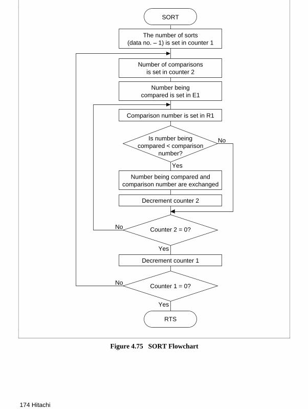
174 Hitachi
Yes
No
RTS
Counter 1 = 0?
The number of sorts(data no. – 1) is set in counter 1
SORT
Number beingcompared is set in E1
Number of comparisonsis set in counter 2
Comparison number is set in R1
Is number beingcompared < comparison
number?
No
Yes
Number being compared andcomparison number are exchanged
Decrement counter 2
Decrement counter 1
Yes
No Counter 2 = 0?
Figure 4.75 SORT Flowchart

Hitachi 175
4.19.6 Program Listing

176 Hitachi
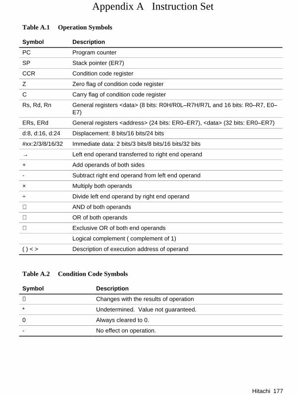
Hitachi 177
Appendix A Instruction Set
Table A.1 Operation Symbols
Symbol Description
PC Program counter
SP Stack pointer (ER7)
CCR Condition code register
Z Zero flag of condition code register
C Carry flag of condition code register
Rs, Rd, Rn General registers <data> (8 bits: R0H/R0L–R7H/R7L and 16 bits: R0–R7, E0–E7)
ERs, ERd General registers <address> (24 bits: ER0–ER7), <data> (32 bits: ER0–ER7)
d:8, d:16, d:24 Displacement: 8 bits/16 bits/24 bits
#xx:2/3/8/16/32 Immediate data: 2 bits/3 bits/8 bits/16 bits/32 bits
→ Left end operand transferred to right end operand
+ Add operands of both sides
- Subtract right end operand from left end operand
× Multiply both operands
÷ Divide left end operand by right end operand
∧ AND of both operands
∨ OR of both operands
⊕ Exclusive OR of both end operands
Logical complement ( complement of 1)
( ) < > Description of execution address of operand
Table A.2 Condition Code Symbols
Symbol Description
↕ Changes with the results of operation
* Undetermined. Value not guaranteed.
0 Always cleared to 0.
- No effect on operation.

178 Hitachi
Notes: 1. (The number of execution states is the value when the operation code and operanddata is in the 2-cycle area that is word accessible, such as on-chip RAM.)
2. For a word-size operation: When there is a carry or borrow to or from bit 11, this bit isset to 1; otherwise, it is cleared to 0.
3. For a longword size operation: When there is a carry or borrow to or from bit 27, this bitis set to 1; otherwise, it is cleared to 0.
4. When the operation result is 0, the value prior to the operation is held; otherwise, it iscleared to 0.
5. Set to 1 when the results of correction causes a carry; otherwise, the value prior to theoperation is held.
6. The number of execution states is 4n+8 when the value set for R4L (for EEPMOV.B) orR4 (for EEPMOV.W) is n.
7. Do not use the E clock synchronous transfer instruction with the H8/3003.
A1 Number of Execution States
The number of execution states for the instruction set is the value when the operation code andoperand data is in the 2-cycle area that is word accessible, such as on-chip RAM. Operation coderesides in external memory, but its attributes (byte/word access, 2/3 state access, wait/not wait,number of waits) can be set with the bus controller and wait state controller. The attributes of theon-chip peripheral modules are fixed and come in two types: 3-state word access modules and 3-state byte access modules. These combinations increase the number of execution states by thenumber of states indicated in the following table.
Table A.3 Increase in Number of Execution States by Operand Data
Access Conditions Data TypeIncrease in Number ofExecution States
External address (2-state byte access) Byte
Word
0
2
External address/on-chip RAM (2-state word access) Byte
Word
0
0
On-chip peripheral module (3-state byte access) Byte
Word
1
4
On-chip peripheral module (3-state word access) Byte
Word
1
1
External address (3-state byte access m cycle wait) Byte
Word
1 + m
4 + 2m
External address (3-state word access m cycle wait) Byte
Word
1 + m
1 + m

Hitachi 179
Table A.4 Increase in Number of Execution States by Operand Code
Access Conditions Increase in Number of Execution States
Instruction Length(Byte) 2 4 6 8 10
External address (2-state byte access) Nonbranch 2 4 6 8 10
Branch 4 6 - - -
External address/on-chip RAM (2-state word access)
Nonbranch 0 0 0 0 0
Branch 0 0 - - -
External address (3-state byte accessm cycle wait)
Nonbranch 4 + 2m 8 + 4m 12 +6m
16 +8m
20 +10m
Branch 8 + 4m 12 +6m
- - -
External address (3-state word accessm cycle wait)
Nonbranch 1 + m 2 + 2m 3 + 3m 4 + 4m 5 + 5m
Branch 2 + 2m 3 + 3m - - -
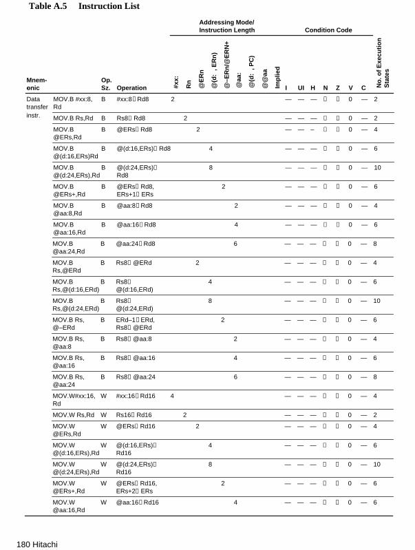
180 Hitachi
Table A.5 Instruction List
Addressing Mode/Instruction Length Condition Code
Mnem--onic
Op.Sz. Operation #x
x:
Rn
@E
Rn
@(d
: ,
ER
n)
@–E
Rn
/@E
RN
+
@aa
:
@(d
: ,
PC
)
@@
aa
Imp
lied
I UI H N Z V C No
. of
Exe
cuti
on
Sta
tes
Datatransfer
MOV.B #xx:8,Rd
B #xx:8→Rd8 2 — — — ↕ ↕ 0 — 2
instr. MOV.B Rs,Rd B Rs8→Rd8 2 — — — ↕ ↕ 0 — 2
MOV.B@ERs,Rd
B @ERs→Rd8 2 — — – ↕ ↕ 0 — 4
MOV.B@(d:16,ERs)Rd
B @(d:16,ERs)→Rd8 4 — — — ↕ ↕ 0 — 6
MOV.B@(d:24,ERs),Rd
B @(d:24,ERs)→Rd8
8 — — — ↕ ↕ 0 — 10
MOV.B@ERs+,Rd
B @ERs→Rd8,ERs+1→ERs
2 — — — ↕ ↕ 0 — 6
MOV.B@aa:8,Rd
B @aa:8→Rd8 2 — — — ↕ ↕ 0 — 4
MOV.B@aa:16,Rd
B @aa:16→Rd8 4 — — — ↕ ↕ 0 — 6
MOV.B@aa:24,Rd
B @aa:24→Rd8 6 — — — ↕ ↕ 0 — 8
MOV.BRs,@ERd
B Rs8→@ERd 2 — — — ↕ ↕ 0 — 4
MOV.BRs,@(d:16,ERd)
B Rs8→
@(d:16,ERd)4 — — — ↕ ↕ 0 — 6
MOV.BRs,@(d:24,ERd)
B Rs8→
@(d:24,ERd)8 — — — ↕ ↕ 0 — 10
MOV.B Rs,@–ERd
B ERd–1→ERd,Rs8→@ERd
2 — — — ↕ ↕ 0 — 6
MOV.B Rs,@aa:8
B Rs8→@aa:8 2 — — — ↕ ↕ 0 — 4
MOV.B Rs,@aa:16
B Rs8→@aa:16 4 — — — ↕ ↕ 0 — 6
MOV.B Rs,@aa:24
B Rs8→@aa:24 6 — — — ↕ ↕ 0 — 8
MOV.W#xx:16,Rd
W #xx:16→Rd16 4 — — — ↕ ↕ 0 — 4
MOV.W Rs,Rd W Rs16→Rd16 2 — — — ↕ ↕ 0 — 2
MOV.W@ERs,Rd
W @ERs→Rd16 2 — — — ↕ ↕ 0 — 4
MOV.W@(d:16,ERs),Rd
W @(d:16,ERs)→Rd16
4 — — — ↕ ↕ 0 — 6
MOV.W@(d:24,ERs),Rd
W @(d:24,ERs)→Rd16
8 — — — ↕ ↕ 0 — 10
MOV.W@ERs+,Rd
W @ERs→Rd16,ERs+2→ERs
2 — — — ↕ ↕ 0 — 6
MOV.W@aa:16,Rd
W @aa:16→Rd16 4 — — — ↕ ↕ 0 — 6
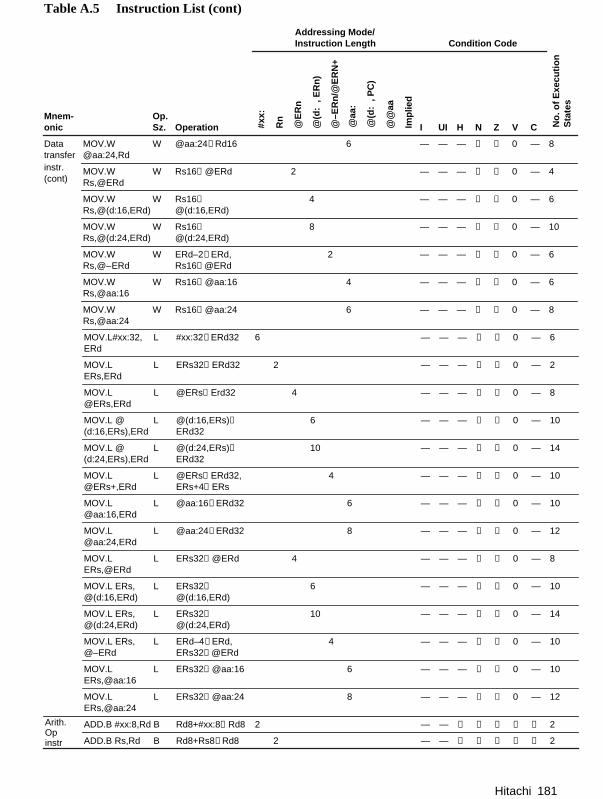
Hitachi 181
Table A.5 Instruction List (cont)
Addressing Mode/Instruction Length Condition Code
Mnem-onic
Op.Sz. Operation #x
x:
Rn
@E
Rn
@(d
: ,
ER
n)
@–E
Rn
/@E
RN
+
@aa
:
@(d
: ,
PC
)
@@
aa
Imp
lied
I UI H N Z V C No
. of
Exe
cuti
on
Sta
tes
Datatransfer
MOV.W@aa:24,Rd
W @aa:24→Rd16 6 — — — ↕ ↕ 0 — 8
instr.(cont)
MOV.WRs,@ERd
W Rs16→@ERd 2 — — — ↕ ↕ 0 — 4
MOV.WRs,@(d:16,ERd)
W Rs16→
@(d:16,ERd)4 — — — ↕ ↕ 0 — 6
MOV.WRs,@(d:24,ERd)
W Rs16→
@(d:24,ERd)8 — — — ↕ ↕ 0 — 10
MOV.W Rs,@– ERd
W ERd–2→ERd,Rs16→@ERd
2 — — — ↕ ↕ 0 — 6
MOV.WRs,@aa:16
W Rs16→@aa:16 4 — — — ↕ ↕ 0 — 6
MOV.WRs,@aa:24
W Rs16→@aa:24 6 — — — ↕ ↕ 0 — 8
MOV.L#xx:32,ERd
L #xx:32→ERd32 6 — — — ↕ ↕ 0 — 6
MOV.LERs,ERd
L ERs32→ERd32 2 — — — ↕ ↕ 0 — 2
MOV.L@ERs,ERd
L @ERs→Erd32 4 — — — ↕ ↕ 0 — 8
MOV.L @(d:16,ERs),ERd
L @(d:16,ERs)→ERd32
6 — — — ↕ ↕ 0 — 10
MOV.L @(d:24,ERs),ERd
L @(d:24,ERs)→ERd32
10 — — — ↕ ↕ 0 — 14
MOV.L@ERs+,ERd
L @ERs→ERd32,ERs+4→ERs
4 — — — ↕ ↕ 0 — 10
MOV.L@aa:16,ERd
L @aa:16→ERd32 6 — — — ↕ ↕ 0 — 10
MOV.L@aa:24,ERd
L @aa:24→ERd32 8 — — — ↕ ↕ 0 — 12
MOV.LERs,@ERd
L ERs32→@ERd 4 — — — ↕ ↕ 0 — 8
MOV.L ERs,@(d:16,ERd)
L ERs32→
@(d:16,ERd)6 — — — ↕ ↕ 0 — 10
MOV.L ERs,@(d:24,ERd)
L ERs32→
@(d:24,ERd)10 — — — ↕ ↕ 0 — 14
MOV.L ERs,@–ERd
L ERd–4→ERd,ERs32→@ERd
4 — — — ↕ ↕ 0 — 10
MOV.LERs,@aa:16
L ERs32→@aa:16 6 — — — ↕ ↕ 0 — 10
MOV.LERs,@aa:24
L ERs32→@aa:24 8 — — — ↕ ↕ 0 — 12
ADD.B #xx:8,Rd B Rd8+#xx:8→Rd8 2 — — ↕ ↕ ↕ ↕ ↕ 2
ADD.B Rs,Rd B Rd8+Rs8→Rd8 2 — — ↕ ↕ ↕ ↕ ↕ 2
Arith. Opinstr
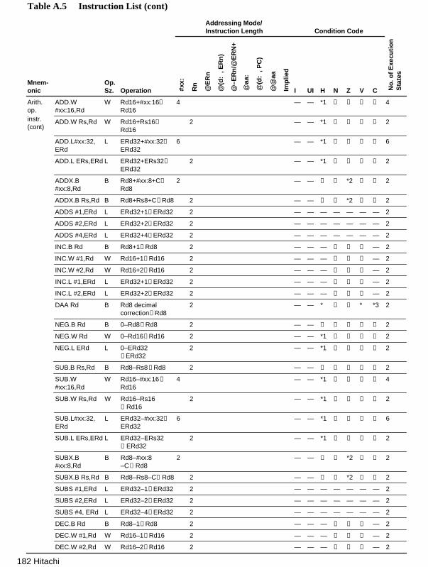
182 Hitachi
Table A.5 Instruction List (cont)
Addressing Mode/Instruction Length Condition Code
Mnem-onic
Op.Sz. Operation #x
x:
Rn
@E
Rn
@(d
: ,
ER
n)
@–E
Rn
/@E
RN
+
@aa
:
@(d
: ,
PC
)
@@
aa
Imp
lied
I UI H N Z V C No
. of
Exe
cuti
on
Sta
tes
Arith.op.
ADD.W#xx:16,Rd
W Rd16+#xx:16→
Rd164 — — *1 ↕ ↕ ↕ ↕ 4
instr.(cont)
ADD.W Rs,Rd W Rd16+Rs16→
Rd162 — — *1 ↕ ↕ ↕ ↕ 2
ADD.L#xx:32,ERd
L ERd32+#xx:32→
ERd326 — — *1 ↕ ↕ ↕ ↕ 6
ADD.L ERs,ERd L ERd32+ERs32→
ERd322 — — *1 ↕ ↕ ↕ ↕ 2
ADDX.B#xx:8,Rd
B Rd8+#xx:8+C→
Rd82 — — ↕ ↕ *2 ↕ ↕ 2
ADDX.B Rs,Rd B Rd8+Rs8+C→Rd8 2 — — ↕ ↕ *2 ↕ ↕ 2
ADDS #1,ERd L ERd32+1→ERd32 2 — — — — — — — 2
ADDS #2,ERd L ERd32+2→ERd32 2 — — — — — — — 2
ADDS #4,ERd L ERd32+4→ERd32 2 — — — — — — — 2
INC.B Rd B Rd8+1→Rd8 2 — — — ↕ ↕ ↕ — 2
INC.W #1,Rd W Rd16+1→Rd16 2 — — — ↕ ↕ ↕ — 2
INC.W #2,Rd W Rd16+2→Rd16 2 — — — ↕ ↕ ↕ — 2
INC.L #1,ERd L ERd32+1→ERd32 2 — — — ↕ ↕ ↕ — 2
INC.L #2,ERd L ERd32+2→ERd32 2 — — — ↕ ↕ ↕ — 2
DAA Rd B Rd8 decimalcorrection→Rd8
2 — — * ↕ ↕ * *3 2
NEG.B Rd B 0–Rd8→Rd8 2 — — ↕ ↕ ↕ ↕ ↕ 2
NEG.W Rd W 0–Rd16→Rd16 2 — — *1 ↕ ↕ ↕ ↕ 2
NEG.L ERd L 0–ERd32→ERd32
2 — — *1 ↕ ↕ ↕ ↕ 2
SUB.B Rs,Rd B Rd8–Rs8→Rd8 2 — — ↕ ↕ ↕ ↕ ↕ 2
SUB.W#xx:16,Rd
W Rd16–#xx:16→
Rd164 — — *1 ↕ ↕ ↕ ↕ 4
SUB.W Rs,Rd W Rd16–Rs16→Rd16
2 — — *1 ↕ ↕ ↕ ↕ 2
SUB.L#xx:32,ERd
L ERd32–#xx:32→
ERd326 — — *1 ↕ ↕ ↕ ↕ 6
SUB.L ERs,ERd L ERd32–ERs32→ERd32
2 — — *1 ↕ ↕ ↕ ↕ 2
SUBX.B#xx:8,Rd
B Rd8–#xx:8– C→Rd8
2 — — ↕ ↕ *2 ↕ ↕ 2
SUBX.B Rs,Rd B Rd8–Rs8–C→Rd8 2 — — ↕ ↕ *2 ↕ ↕ 2
SUBS #1,ERd L ERd32–1→ERd32 2 — — — — — — — 2
SUBS #2,ERd L ERd32–2→ERd32 2 — — — — — — — 2
SUBS #4, ERd L ERd32–4→ERd32 2 — — — — — — — 2
DEC.B Rd B Rd8–1→Rd8 2 — — — ↕ ↕ ↕ — 2
DEC.W #1,Rd W Rd16–1→Rd16 2 — — — ↕ ↕ ↕ — 2
DEC.W #2,Rd W Rd16–2→Rd16 2 — — — ↕ ↕ ↕ — 2
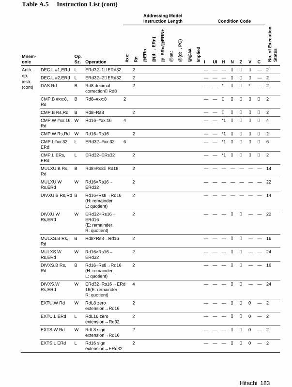
Hitachi 183
Table A.5 Instruction List (cont)
Addressing Mode/Instruction Length Condition Code
Mnem-onic
Op.Sz. Operation #x
x:
Rn
@E
Rn
@(d
: ,
ER
n)
@–E
Rn
/@E
RN
+
@aa
:
@(d
: ,
PC
)
@@
aa
Imp
lied
I UI H N Z V C No
. of
Exe
cuti
on
Sta
tes
Arith. DEC.L #1,ERd L ERd32–1→ERd32 2 — — — ↕ ↕ ↕ — 2op. DEC.L #2,ERd L ERd32–2→ERd32 2 — — — ↕ ↕ ↕ — 2instr.(cont) DAS Rd B Rd8 decimal
correction→Rd82 — — * ↕ ↕ * — 2
CMP.B #xx:8,Rd
B Rd8–#xx:8 2 — — ↕ ↕ ↕ ↕ ↕ 2
CMP.B Rs,Rd B Rd8–Rs8 2 — — ↕ ↕ ↕ ↕ ↕ 2
CMP.W #xx:16,Rd
W Rd16–#xx:16 4 — — *1 ↕ ↕ ↕ ↕ 4
CMP.W Rs,Rd W Rd16–Rs16 2 — — *1 ↕ ↕ ↕ ↕ 2
CMP.L#xx:32,ERd
L ERd32–#xx:32 6 — — *1 ↕ ↕ ↕ ↕ 6
CMP.L ERs,ERd
L ERd32–ERs32 2 — — *1 ↕ ↕ ↕ ↕ 2
MULXU.B Rs,Rd
B Rd8×Rs8→Rd16 2 — — — — — — — 14
MULXU.WRs,ERd
W Rd16×Rs16→ERd32
2 — — — — — — — 22
DIVXU.B Rs,Rd B Rd16÷Rs8→Rd16(H: remainderL: quotient)
2 — — — — — — — 14
DIVXU.WRs,ERd
W ERd32÷Rs16→ERd16(E: remainder,R: quotient)
2 — — — ↕ ↕ — — 22
MULXS.B Rs,Rd
B Rd8×Rs8→Rd16 2 — — — ↕ ↕ — — 16
MULXS.WRs,ERd
W Rd16×Rs16→ERd32
2 — — — ↕ ↕ — — 24
DIVXS.B Rs,Rd
B Rd16÷Rs8→Rd16(H: remainder,L: quotient)
2 — — — ↕ ↕ — — 16
DIVXS.WRs,ERd
W ERd32÷Rs16→ERd16(E: remainder,R: quotient)
4 — — — ↕ ↕ — — 24
EXTU.W Rd W RdL8 zeroextension→Rd16
2 — — — ↕ ↕ 0 — 2
EXTU.L ERd L RdL16 zeroextension→Rd32
2 — — — ↕ ↕ 0 — 2
EXTS.W Rd W RdL8 signextension→Rd16
2 — — — ↕ ↕ 0 — 2
EXTS.L ERd L Rd16 signextension→ERd32
2 — — — ↕ ↕ 0 — 2

184 Hitachi
Table A.5 Instruction List (cont)
Addressing Mode/Instruction Length Condition Code
Mnem-onic
Op.Sz. Operation #x
x:
Rn
@E
Rn
@(d
: ,
ER
n)
@–E
Rn
/@E
RN
+
@aa
:
@(d
: ,
PC
)
@@
aa
Imp
lied
I UI H N Z V C No
. of
Exe
cuti
on
Sta
tes
Logical AND.B #xx:8,Rd B Rd8∧#xx:8→Rd8 2 — — — ↕ ↕ 0 — 2op. AND.B Rs,Rd B Rd8∧Rs8→Rd8 2 — — — ↕ ↕ 0 — 2instr.
AND.W#xx:16,Rd
W Rd16∧#xx:16→RD16
Rd16
4 — — — ↕ ↕ 0 — 4
AND.W Rs,Rd W Rd16∧Rs16→ 2 — — — ↕ ↕ 0 — 2
AND.L#xx:32,ERd
L ERd32∧#xx:32→ERd32
6 — — — ↕ ↕ 0 — 6
AND.L ERs,ERd L ERd32∧ERs32→ERd32
4 — — — ↕ ↕ 0 — 4
OR.B #xx:8,Rd B Rd8∨#xx:8→Rd8 2 — — — ↕ ↕ 0 — 2
OR.B Rs,Rd B Rd8∨Rs8→Rd8 2 — — — ↕ ↕ 0 — 2
OR.W#xx:16,Rd
W Rd16∨#xx:16→Rd16
4 — — — ↕ ↕ 0 — 4
OR.W Rs,Rd W Rd16∨Rs16→Rd16
2 — — — ↕ ↕ 0 — 2
OR.L #xx:32,ERd
L ERd32∨#xx:32→ERd32
6 — — — ↕ ↕ 0 — 6
OR.L ERs,ERd L ERd32∨ERs32→ERd32
4 — — — ↕ ↕ 0 — 4
XOR.B #xx:8,Rd
B Rd8⊕#xx:8→Rd8 2 — — — ↕ ↕ 0 — 2
XOR.B Rs,Rd B Rd8⊕Rs8→Rd8 2 — — — ↕ ↕ 0 — 2
XOR.W#xx:16,Rd
W Rd16⊕#xx:16→Rd16
4 — — — ↕ ↕ 0 — 4
XOR.W Rs,Rd W Rd16⊕Rs16→Rd16 2 — — — ↕ ↕ 0 — 2
XOR.L#xx:32,ERd
L ERd32⊕#xx:32→ERd32
6 — — — ↕ ↕ 0 — 6
XOR.L ERs,ERd
L ERd32⊕ERs32→ERd32
4 — — — ↕ ↕ 0 — 4
NOT.B Rd B Rd8→Rd8 2 — — — ↕ ↕ 0 — 2
NOT.W Rd W Rd16→Rd16 2 — — — ↕ ↕ 0 — 2
NOT.L ERd L ERd32→ERd32 2 — — — ↕ ↕ 0 — 2
Shiftinstr.
SHAL.B Rd B Rd8 left arithmeticshift→Rd8
2 — — — ↕ ↕ ↕ ↕ 2
SHAL.W Rd W Rd16 leftarithmeticshift→Rd16
2 — — — ↕ ↕ ↕ ↕ 2
SHAL.L ERd L ERd32 leftarithmeticshift→ERd32
2 — — — ↕ ↕ ↕ ↕ 2
SHAR.B Rd B Rd8 rightarithmeticshift→Rd8
2 — — — ↕ ↕ 0 ↕ 2
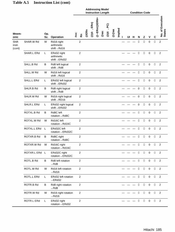
Hitachi 185
Table A.5 Instruction List (cont)
Addressing Mode/Instruction Length Condition Code
Mnem-onic
Op.Sz. Operation #x
x:
Rn
@E
Rn
@(d
: ,
ER
n)
@–E
Rn
/@E
RN
+
@aa
:
@(d
: ,
PC
)
@@
aa
Imp
lied
I UI H N Z V C No
. of
Exe
cuti
on
Sta
tes
Shiftinstr.(cont)
SHAR.W Rd W Rd16 rightarithmeticshift→Rd16
2 — — — ↕ ↕ 0 ↕ 2
SHAR.L ERd L ERd32 rightarithmeticshift→ERd32
2 — — — ↕ ↕ 0 ↕ 2
SHLL.B Rd B Rd8 left logicalshift→Rd8
2 — — — ↕ ↕ 0 ↕ 2
SHLL.W Rd W Rd16 left logicalshift→Rd16
2 — — — ↕ ↕ 0 ↕ 2
SHLL.L ERd L ERd32 left logicalshift→ERd32
2 — — — ↕ ↕ 0 ↕ 2
SHLR.B Rd B Rd8 right logicalshift→Rd8
2 — — — 0 ↕ 0 ↕ 2
SHLR.W Rd W Rd16 right logicalshift→RD16
2 — — — 0 ↕ 0 ↕ 2
SHLR.L ERd L ERd32 right logicalshift→ERd32
2 — — — 0 ↕ 0 ↕ 2
ROTXL.B Rd B Rd8C leftrotation→Rd8C
2 — — — ↕ ↕ 0 ↕ 2
ROTXL.W Rd W Rd16C leftrotation→Rd16C
2 — — — ↕ ↕ 0 ↕ 2
ROTXL.L ERd L ERd32C leftrotation→ERd32C
2 — — — ↕ ↕ 0 ↕ 2
ROTXR.B Rd B Rd8C rightrotation→Rd8C
2 — — — ↕ ↕ 0 ↕ 2
ROTXR.W Rd W Rd16C rightrotation→Rd16C
2 — — — ↕ ↕ 0 ↕ 2
ROTXR.L ERd L ERd32C rightrotation→ERd32C
2 — — — ↕ ↕ 0 ↕ 2
ROTL.B Rd B Rd8 left rotation→Rd8
2 — — — ↕ ↕ 0 ↕ 2
ROTL.W Rd W Rd16 left rotation→Rd16
2 — — — ↕ ↕ 0 ↕ 2
ROTL.L ERd L ERd32 left rotation→ERd32
2 — — — ↕ ↕ 0 ↕ 2
ROTR.B Rd B Rd8 right rotation→Rd8
2 — — — ↕ ↕ 0 ↕ 2
ROTR.W Rd W Rd16 right rotation→Rd16
2 — — — ↕ ↕ 0 ↕ 2
ROTR.L ERd L ERd32 rightrotation→ERd32
2 — — — ↕ ↕ 0 ↕ 2
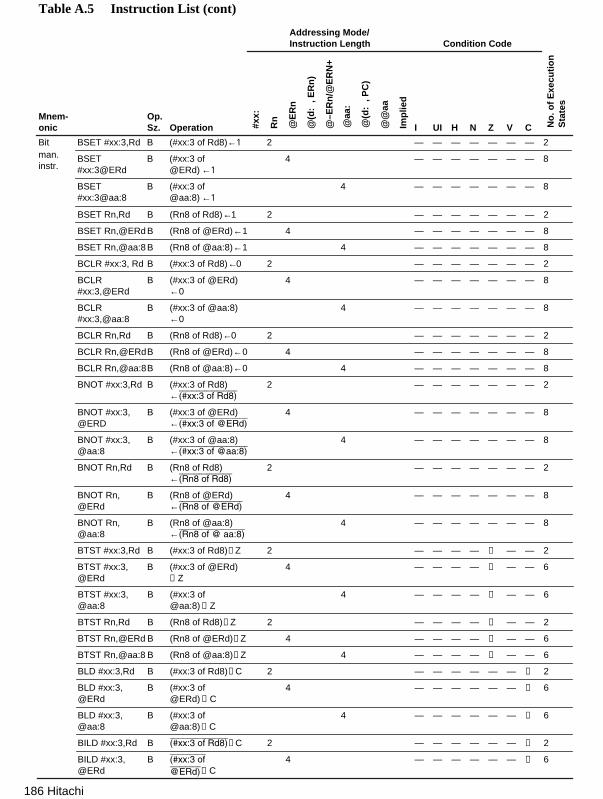
186 Hitachi
Table A.5 Instruction List (cont)
Addressing Mode/Instruction Length Condition Code
Mnem-onic
Op.Sz. Operation #x
x:
Rn
@E
Rn
@(d
: ,
ER
n)
@–E
Rn
/@E
RN
+
@aa
:
@(d
: ,
PC
)
@@
aa
Imp
lied
I UI H N Z V C No
. of
Exe
cuti
on
Sta
tes
BSET Rn,Rd B (Rn8 of Rd8)←1 2 — — — — — — — 2
BSET Rn,@ERd B (Rn8 of @ERd)←1 4 — — — — — — — 8
BSET Rn,@aa:8 B (Rn8 of @aa:8)←1 4 — — — — — — — 8
BCLR #xx:3, Rd B (#xx:3 of Rd8)←0 2 — — — — — — — 2
BCLR#xx:3,@ERd
B (#xx:3 of @ERd)←0
4 — — — — — — — 8
BCLR#xx:3,@aa:8
B (#xx:3 of @aa:8)←0
4 — — — — — — — 8
BCLR Rn,Rd B (Rn8 of Rd8)←0 2 — — — — — — — 2
BCLR Rn,@ERdB (Rn8 of @ERd)←0 4 — — — — — — — 8
BCLR Rn,@aa:8B (Rn8 of @aa:8)←0 4 — — — — — — — 8
BNOT #xx:3,Rd B (#xx:3 of Rd8)←(#xx:3 of Rd8)
2 — — — — — — — 2
BNOT #xx:3,@ERD
B (#xx:3 of @ERd)←(#xx:3 of @ERd)
4 — — — — — — — 8
BNOT #xx:3,@aa:8
B (#xx:3 of @aa:8)←(#xx:3 of @aa:8)
4 — — — — — — — 8
BNOT Rn,Rd B (Rn8 of Rd8)←(Rn8 of Rd8)
2 — — — — — — — 2
BNOT Rn,@ERd
B (Rn8 of @ERd)←(Rn8 of @ERd)
4 — — — — — — — 8
BNOT Rn,@aa:8
B (Rn8 of @aa:8)←(Rn8 of @ aa:8)
4 — — — — — — — 8
BTST #xx:3,Rd B (#xx:3 of Rd8)→Z 2 — — — — ↕ — — 2
BTST #xx:3,@ERd
B (#xx:3 of @ERd)→Z
4 — — — — ↕ — — 6
BTST #xx:3,@aa:8
B (#xx:3 of @aa:8) →Z
4 — — — — ↕ — — 6
BTST Rn,Rd B (Rn8 of Rd8)→Z 2 — — — — ↕ — — 2
BTST Rn,@ERd B (Rn8 of @ERd)→Z 4 — — — — ↕ — — 6
BTST Rn,@aa:8 B (Rn8 of @aa:8)→Z 4 — — — — ↕ — — 6
BLD #xx:3,Rd B (#xx:3 of Rd8)→C 2 — — — — — — ↕ 2
BLD #xx:3,@ERd
B (#xx:3 of @ERd) →C
4 — — — — — — ↕ 6
BLD #xx:3,@aa:8
B (#xx:3 of @aa:8)→C
4 — — — — — — ↕ 6
BILD #xx:3,Rd B (#xx:3 of Rd8)→C 2 — — — — — — ↕ 2
BILD #xx:3,@ERd
B (#xx:3 of @ERd)→C
4 — — — — — — ↕ 6
Bit BSET #xx:3,Rd B (#xx:3 of Rd8)←1 2 — — — — — — — 2man.instr.
BSET#xx:3@ERd
B (#xx:3 of @ERd) ←1
4 — — — — — — — 8
BSET#xx:3@aa:8
B (#xx:3 of @aa:8) ←1
4 — — — — — — — 8
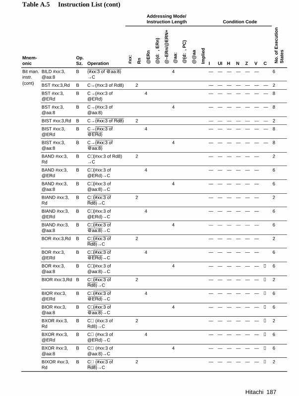
Hitachi 187
Table A.5 Instruction List (cont)
Addressing Mode/Instruction Length Condition Code
Mnem-onic
Op.Sz. Operation #x
x:
Rn
@E
Rn
@(d
: ,
ER
n)
@–E
Rn
/@E
RN
+
@aa
:
@(d
: ,
PC
)
@@
aa
Imp
lied
I UI H N Z V C No
. of
Exe
cuti
on
Sta
tes
Bit man.instr.
BILD #xx:3,@aa:8
B (#xx:3 of @aa:8)→C
4 — — — — — — 6
(cont) BST #xx:3,Rd B C→(#xx:3 of Rd8) 2 — — — — — — — 2
BST #xx:3,@ERd
B C→(#xx:3 of@ERd)
4 — — — — — — — 8
BST #xx:3,@aa:8
B C→(#xx:3 of@aa:8)
4 — — — — — — — 8
BIST #xx:3,Rd B C→(#xx:3 of Rd8) 2 — — — — — — — 2
BIST #xx:3,@ERd
B C→(#xx:3 of @ERd)
4 — — — — — — — 8
BIST #xx:3,@aa:8
B C→(#xx:3 of @aa:8)
4 — — — — — — — 8
BAND #xx:3,Rd
B C∧(#xx:3 of Rd8)→C
2 — — — — — — 2
BAND #xx:3,@ERd
B C∧(#xx:3 of@ERd)→C
4 — — — — — — 6
BAND #xx:3,@aa:8
B C∧(#xx:3 of@aa:8)→C
4 — — — — — — 6
BIAND #xx:3,Rd
B C∧(#xx:3 of Rd8)→C
2 — — — — — — 2
BIAND #xx:3,@ERd
B C∧(#xx:3 of@ERd)→C
4 — — — — — — 6
BIAND #xx:3,@aa:8
B C∧(#xx:3 of @aa:8)→C
4 — — — — — — 6
BOR #xx:3,Rd B C∨(#xx:3 of Rd8)→C
2 — — — — — — 2
BOR #xx:3,@ERd
B C∨(#xx:3 of @ERd)→C
4 — — — — — — 6
BOR #xx:3,@aa:8
B C∨(#xx:3 of@aa:8)→C
4 — — — — — — ↕ 6
BIOR #xx:3,Rd B C∨(#xx:3 of Rd8)→C
2 — — — — — — ↕ 2
BIOR #xx:3,@ERd
B C∨(#xx:3 of @ERd)→C
4 — — — — — — ↕ 6
BIOR #xx:3,@aa:8
B C∨(#xx:3 of @aa:8)→C
4 — — — — — — ↕ 6
BXOR #xx:3,Rd
B C⊕ (#xx:3 ofRd8)→C
2 — — — — — — ↕ 2
BXOR #xx:3,@ERd
B C⊕ (#xx:3 of@ERd)→C
4 — — — — — — ↕ 6
BXOR #xx:3,@aa:8
B C⊕ (#xx:3 of@aa:8)→C
4 — — — — — — ↕ 6
BIXOR #xx:3,Rd
B C⊕ (#xx:3 of Rd8)→C
2 — — — — — — ↕ 2
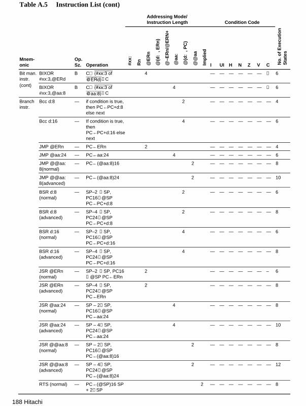
188 Hitachi
Table A.5 Instruction List (cont)
Addressing Mode/Instruction Length Condition Code
Mnem-onic
Op.Sz. Operation #x
x:
Rn
@E
Rn
@(d
: ,
ER
n)
@–E
Rn
/@E
RN
+
@aa
:
@(d
: ,
PC
)
@@
aa
Imp
lied
I UI H N Z V C No
. of
Exe
cuti
on
Sta
tes
Bit man.instr.
BIXOR#xx:3,@ERd
B C@ERd)
⊕ (#xx:3 of→C
4 — — — — — — ↕ 6
(cont) BIXOR#xx:3,@aa:8
B C@aa:8)
⊕ (#xx:3 of→C
4 — — — — — — ↕ 6
Branchinstr.
Bcc d:8 — if condition is true,then PC←PC+d:8else next
2 — — — — — — — 4
Bcc d:16 — If condition is true,thenPC←PC+d:16 elsenext
4 — — — — — — — 6
JMP @ERn — PC←ERn 2 — — — — — — — 4
JMP @aa:24 — PC←aa:24 4 — — — — — — — 6
JMP @@aa:8(normal)
— PC←(@aa:8)16 2 — — — — — — — 8
BSR d:8(normal)
— SP–2 →SP,PC16→@SPPC←PC+d:8
2 — — — — — — — 6
BSR d:8(advanced)
— SP–4 →SP,PC24→@SPPC←PC+d:8
2 — — — — — — — 8
BSR d:16(normal)
— SP–2 →SP,PC16→@SPPC←PC+d:16
4 — — — — — — — 6
BSR d:16(advanced)
— SP–4 →SP,PC24→@SPPC←PC+d:16
4 — — — — — — — 8
JSR @ERn(normal)
— SP–2 →SP, PC16→@SP PC←ERn
2 — — — — — — – 6
JSR @ERn(advanced)
— SP–4 →SP,PC24→@SPPC←ERn
2 — — — — — — — 8
JSR @aa:24(normal)
— SP – 2→SP,PC16→@SPPC←aa:24
4 — — — — — — — 8
JSR @aa:24(advanced)
— SP – 4→SP,PC24→@SPPC←aa:24
4 — — — — — — — 10
JSR @@aa:8(normal)
— SP – 2→SP,PC16→@SPPC←(@aa:8)16
2 — — — — — — — 8
JSR @@aa:8(advanced)
— SP – 4→SP,PC24→@SPPC←(@aa:8)24
2 — — — — — — — 12
RTS (normal) — PC←(@SP)16 SP+ 2→SP
2 — — — — — — — 8
JMP @@aa:8(advanced)
— PC←(@aa:8)24 2 — — — — — — — 10
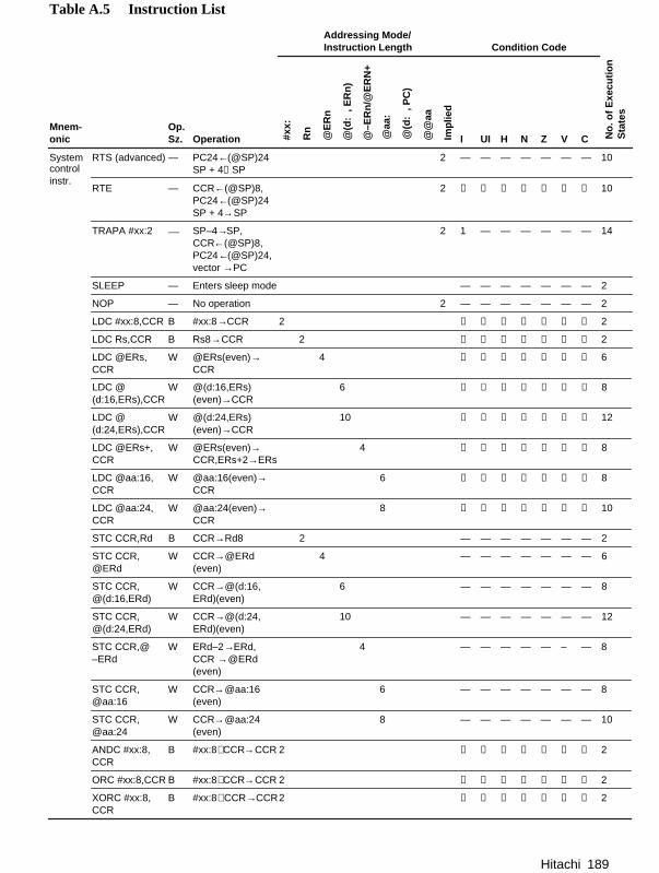
Hitachi 189
Table A.5 Instruction List
Addressing Mode/Instruction Length Condition Code
Mnem-onic
Op.Sz. Operation #x
x:
Rn
@E
Rn
@(d
: ,
ER
n)
@–E
Rn
/@E
RN
+
@aa
:
@(d
: ,
PC
)
@@
aa
Imp
lied
I UI H N Z V C No
. of
Exe
cuti
on
Sta
tes
Systemcontrolinstr.
RTE — CCR←(@SP)8,PC24←(@SP)24SP + 4→SP
2 ↕ ↕ ↕ ↕ ↕ ↕ ↕ 10
TRAPA #xx:2 — SP–4→SP,CCR←(@SP)8,PC24←(@SP)24,vector →PC
2 1 — — — — — — 14
SLEEP — Enters sleep mode — — — — — — — 2
NOP — No operation 2 — — — — — — — 2
LDC #xx:8,CCR B #xx:8→CCR 2 ↕ ↕ ↕ ↕ ↕ ↕ ↕ 2
LDC Rs,CCR B Rs8→CCR 2 ↕ ↕ ↕ ↕ ↕ ↕ ↕ 2
LDC @ERs,CCR
W @ERs(even)→CCR
4 ↕ ↕ ↕ ↕ ↕ ↕ ↕ 6
LDC @(d:16,ERs),CCR
W @(d:16,ERs)(even)→CCR
6 ↕ ↕ ↕ ↕ ↕ ↕ ↕ 8
LDC @(d:24,ERs),CCR
W @(d:24,ERs)(even)→CCR
10 ↕ ↕ ↕ ↕ ↕ ↕ ↕ 12
LDC @ERs+,CCR
W @ERs(even)→CCR,ERs+2→ERs
4 ↕ ↕ ↕ ↕ ↕ ↕ ↕ 8
LDC @aa:16,CCR
W @aa:16(even)→CCR
6 ↕ ↕ ↕ ↕ ↕ ↕ ↕ 8
LDC @aa:24,CCR
W @aa:24(even)→CCR
8 ↕ ↕ ↕ ↕ ↕ ↕ ↕ 10
STC CCR,Rd B CCR→Rd8 2 — — — — — — — 2
STC CCR,@ERd
W CCR→@ERd(even)
4 — — — — — — — 6
STC CCR,@(d:16,ERd)
W CCR→@(d:16,ERd)(even)
6 — — — — — — — 8
STC CCR,@(d:24,ERd)
W CCR→@(d:24,ERd)(even)
10 — — — — — — — 12
STC CCR,@– ERd
W ERd–2→ERd,CCR →@ERd(even)
4 — — — — — – — 8
STC CCR,@aa:16
W CCR→@aa:16(even)
6 — — — — — — — 8
STC CCR,@aa:24
W CCR→@aa:24(even)
8 — — — — — — — 10
ANDC #xx:8,CCR
B #xx:8∧CCR→CCR 2 ↕ ↕ ↕ ↕ ↕ ↕ ↕ 2
ORC #xx:8,CCR B #xx:8∨CCR→CCR 2 ↕ ↕ ↕ ↕ ↕ ↕ ↕ 2
XORC #xx:8,CCR
B #xx:8⊕CCR→CCR2 ↕ ↕ ↕ ↕ ↕ ↕ ↕ 2
RTS (advanced) — PC24←(@SP)24SP + 4→SP
2 — — — — — — — 10

190 Hitachi
Appendix B AssemblerControl Instruction Functions
B.1 .CPU
Specifies the CPU.
Format:
Label Operation Operand
x .CPU CPU type
Note: CPU type: {300HA | 300HN | 300 | 300L}
Description: Specifies the CPU that the source program to be assembled is for. The assemblerassembles it for the specified CPU.
CPU types are as follows:
• 300HA H8/300H advanced mode
• 300HN H8/300H normal mode
• 300 H8/300
• 300L H8/300L
When this control instruction is omitted, 300HA is set.
This control instruction should be stated at the start of the source program. If there is nothing atthe start of the source program except the control instruction for the assembler list, an error willresult.
This control instruction is valid only once. It is valid when there is no /CPU command line optionspecified.
Example:
.CPU: 300HA
.SECTION A, CODE, ALIGN = 2MOV.W R0, R1MOV.W R0, R2
Assembles for H8/300H, advanced mode.

Hitachi 191
B.2 .SECTION
Declares the section.
Format:
Label Operation Operand
x .SECTION Section name [, sectionattributes [, format type]] type
Note: Section attributes: {CODE | DATA | STACK | COMMON | DUMMY}
Format type: {LOCATE = start address|ALIGN = boundary adjust number}
Description: Declares the start and restart of the section.
• Section start: Starts the section and sets the section name, section attributes and type of format.
— Section name: Specifies the section name. Section names are written the same as symbolnames. Case is not distinguished.
— Section attributes: Sets the section attributes. Section attributes are as follows:
CODE: Code section
DATA: Data section
STACK: Stack section
COMMON: Common section
DUMMY: Dummy section
When no attribute is specified, CODE is set.
— Format type: Sets the format type:
LOCATE = start address Absolute addressingALIGN = boundary adjust number Relative addressing
When no format is specified, ALIGN = 2 is set.
With absolute addressing, the start address of the section is set. The start address is specified as arear-referenced absolute value. The maximum start address values are as follows:
• H8/300H advanced mode: H'00FFFFFF
• H8/300H normal mode: H'0000FFFF
• H8/300: H'0000FFFF
• H8/300L: H'0000FFFF
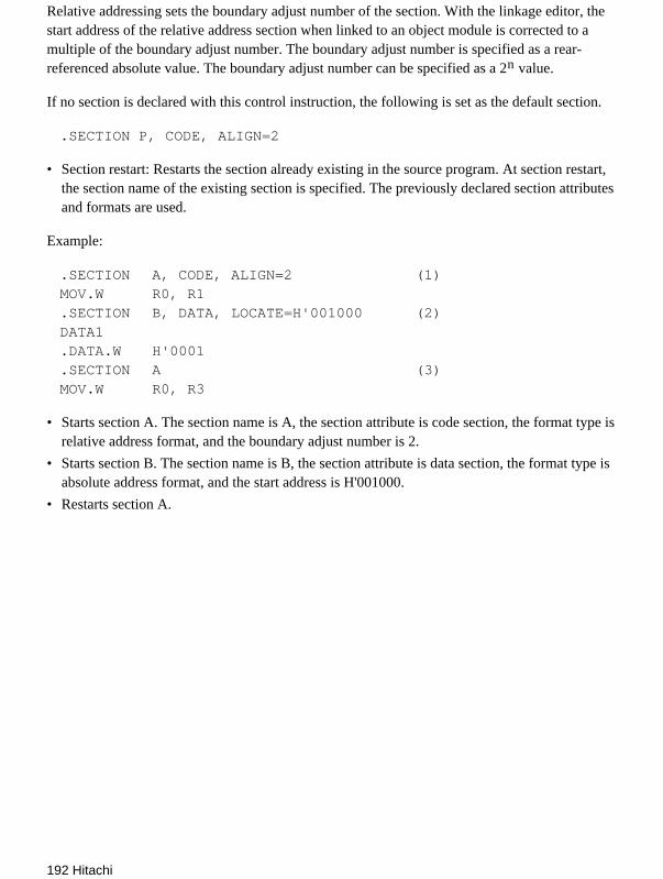
192 Hitachi
Relative addressing sets the boundary adjust number of the section. With the linkage editor, thestart address of the relative address section when linked to an object module is corrected to amultiple of the boundary adjust number. The boundary adjust number is specified as a rear-referenced absolute value. The boundary adjust number can be specified as a 2n value.
If no section is declared with this control instruction, the following is set as the default section.
.SECTION P, CODE, ALIGN=2
• Section restart: Restarts the section already existing in the source program. At section restart,the section name of the existing section is specified. The previously declared section attributesand formats are used.
Example:
.SECTION A, CODE, ALIGN=2 (1)MOV.W R0, R1.SECTION B, DATA, LOCATE=H'001000 (2)DATA1.DATA.W H'0001.SECTION A (3)MOV.W R0, R3
• Starts section A. The section name is A, the section attribute is code section, the format type isrelative address format, and the boundary adjust number is 2.
• Starts section B. The section name is B, the section attribute is data section, the format type isabsolute address format, and the start address is H'001000.
• Restarts section A.
Hitachi 193
B.3 .EQU
Sets the symbol value.
Format:
Label Operation Operand
Symbol name .EQU Number
Description: Sets a value for the symbol. The value is set as a rear-referenced absolute value or arear-referenced address value. The symbol value defined by this control instruction cannot bechanged.
Example:
SYM1 .EQU 1SYM2 .EQU 2.SECTION A, CODE, ALIGN = 2MOV.B #SYM1:8, R0L… Same as MOV.B #1:8, R0LMOV.B #SYM2:8, R1L… Same as MOV.B #2:8, R1L
Sets 1 for SYM1 and 2 for SYM2.
194 Hitachi
B.4 .ORG
Sets the location counter value.
Format:
Label Operation Operand
x .ORG Location counter value
Description: Changes the location counter value in the section to the specified value.
The location counter value is specified as a rear-referenced absolute value or as a rear-referencedaddress value of the section itself. The maximum location counter values are as follows.
H8/300H advanced mode: H'00FFFFFFH8/300H normal mode: H'0000FFFFH8/300: H'0000FFFFH8/300L: H'0000FFFF
When specified in the absolute address section, the location counter value specified must be avalue after the start address of the section. When this control instruction is specified in theabsolute address section, the set location counter value becomes an absolute address; whenspecified in the relative address section, it becomes a relative address.
Example:
.SECTION A, DATA, ALIGN = 2DATA1.DATA.W H'0001.DATA.W H'0002.ORG H'000100 (1)DATA2.DATA.W H'0003.DATA.W H'0004
(1) The location counter value is changed to the relative H'000100 address for A.

Hitachi 195
B.5 .DATA
Reserves integer data.
Format:
Label Operation Operand
x .DATA [. s] Integer data [, integer data …]
Note: s (size): {B|W|L}
Description: Reserves integer data according to the size specified.
The sizes are as follows.
• B: Byte (1 byte)
• W: Word (2 byte)
• L: Longword (4 bytes)
When not specified, B is set.
The following integer data values can be specified according to size.
• B: –128 to 255
• W: –32,768 to 65,535
• L: –2,147,483,648 to 4,294,967,295
Example:
.SECTION A, DATA, ALIGN = 2
.DATA.W H'0102, H'0304
.DATA.B H'05, H'06, H'07, H'08
Data is reserved as follows:
01 02 03 04 05 06 07 08
196 Hitachi
B.6 .RES
Reserves the integer data region.
Format:
Label Operation Operand
[Symbol name] .RES [. s] Number of regions
Note: s (size): {B|W|L}
Description: Reserves integer data regions. A region of exactly the size specified for the integerdata region is ensured.
The sizes are as follows:
• B: Byte (1 byte)
• W: Word (2 byte)
• L: Longword (4 bytes)
When not specified, B is set.
The number of regions is specified as a rear-referenced absolute value. Any number higher than 1can be specified.
Example:
.SECTION A, DATA, ALIGN = 2
.RES.W 10
.RES.B 255
A 20 byte region and a 255 byte region are kept.

Hitachi 197
B.7 .END
End of source program.
Format:
Label Operation Operand
x .END [Execution start address]
Description: Indicates the end of the source program. When this control instruction appears, theassembler quits assembling. The execution start address allows you to specify the address usedwhen the simulation is started on a simulation debugger. The code section address is set for theexecution start address. The execution start address is specified as an absolute value or addressvalue.
Example:
.CPU 300HA
.OUTPUT DBG:.SECTION A, CODE, ALIGN = 2STARTMOV.L #0:32, ER0MOV.L #1:32, ER1MOV.L #2:32, ER2BRA START:8;.END START
In the simulation debugger, the simulation starts from the START address.