high-voltage, step down controller in tsot6 · 2014-05-10 · 0.6v reference voltage 1% output...
TRANSCRIPT
Nov
Nov07-08 RevG SP6126: TSOT-6 PFET Buck Controller 2008 Exar Corporation
1
FEATURES Wide 4.5V – 29V Input Voltage Range Internal Compensation Built-in High Current PMOS Driver Adjustable Overcurrent Protection Internal soft-start 600kHz Constant Frequency Operation 0.6V Reference Voltage 1% output setpoint accuracy Lead Free, RoHS Compliant Package:
Small 6-Pin TSOT
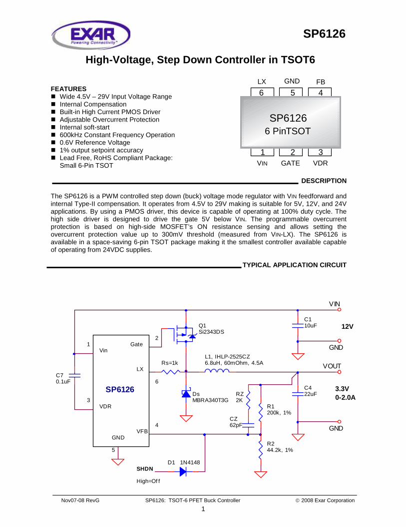
DESCRIPTION The SP6126 is a PWM controlled step down (buck) voltage mode regulator with VIN feedforward and internal Type-II compensation. It operates from 4.5V to 29V making is suitable for 5V, 12V, and 24V applications. By using a PMOS driver, this device is capable of operating at 100% duty cycle. The high side driver is designed to drive the gate 5V below VIN. The programmable overcurrent protection is based on high-side MOSFET’s ON resistance sensing and allows setting the overcurrent protection value up to 300mV threshold (measured from VIN-LX). The SP6126 is available in a space-saving 6-pin TSOT package making it the smallest controller available capable of operating from 24VDC supplies.
TYPICAL APPLICATION CIRCUIT
6 5 4
1 2 3
SP61266 PinTSOT
GNDLX
GATE
FB
VIN VDR
High=Of f
L1, IHLP-2525CZ6.8uH, 60mOhm, 4.5A
C422uFDs
MBRA340T3GR1200k, 1%
RZ2K
R244.2k, 1%
Q1Si2343DS
CZ62pF
C70.1uF
C110uF
Rs=1k
D1 1N4148
12V
SHDN
VIN
GND
GND
VOUT
Vin
GND
VDR
VFB
Gate
LX
SP6126 3.3V0-2.0A
5
3
12
6
4
SP6126
High-Voltage, Step Down Controller in TSOT6

Nov07-08 RevG SP6126: TSOT-6 PFET Buck Controller 2008 Exar Corporation
2
These are stress ratings only, and functional operation of the device at these ratings or any other above those indicated in the operation sections of the specifications below is not implied. Exposure to absolute maximum rating conditions for extended periods of time may affect reliability.
ABSOLUTE MAXIMUM RATINGS
Input Voltage….................................................-0.3V to 30V Lx………………………………………………….…-2V to 30V FB……………..................................................-0.3V to 5.5V Storage Temperature..………………...……-65 °C to 150 °C Junction Temperature...................................-40°C to 125°C Lead Temperature (Soldering, 10 sec)….….………..300 °C ESD Rating……….….…1kV LX, 2kV all other nodes, HBM
ELECTRICAL SPECIFICATIONS Specifications are for TAMB=TJ=25°C, and those denoted by ♦ apply over the full operating range, -40°C< Tj <125°C. Unless otherwise specified: VIN =4.5V to 29V, CIN = 4.7µF.
PARAMETER MIN TYP MAX UNITS ♦ CONDITIONS
UVLO Turn-On Threshold 4.2 4.35 4.5 V 0°C< Tj <125°C
UVLO Turn-Off Threshold 4.0 4.2 4.4 V 0°C< Tj <125°C
UVLO Hysterisis 0.2 V
Operating Input Voltage Range 4.5 29 V 0°C< Tj <125°C
Operating Input Voltage Range 7 29 V ♦
Operating VCC Current 0.3 3 mA VFB=1.2V
Reference Voltage Accuracy 0.5 %
Reference Voltage Accuracy 0.5 2 % ♦
Reference Voltage 0.6 V
Reference Voltage 0.588 0.6 0.612 V ♦
Switching Frequency 510 600 690 kHz Peak-to-peak ramp Modulator VIN/5 V
Minimum ON-Time Duration 40 100 ns ♦
Minimum Duty Cycle 0 % Maximum Duty Cycle 100 % Gate Driver Turn-Off Resistance 50 60 kΩ Internal resistor between GATE and
VIN Gate Driver Pull-Down Resistance 4 8 Ω VIN=12V, VFB=0.5V, Measure
resistance between GATE and VDR Gate Driver Pull-up Resistance
3 6 Ω VIN=12V, VFB=0.7V, Measure resistance between GATE and VIN
VIN - VDR voltage difference 4.5 5.5 V ♦ Measure VIN – VDR, VIN>7V
Overcurrent Threshold 270 300 330 mV Measure VIN - LX
LX pin Input Current 25 30 35 uA VLX = VIN OFF interval during hiccup 100 ms
Soft start time 3 5 9 ms VFB=0.58V, measure between VIN=4.5V and first GATE pulse
SHDN Threshold 0.9 1.0 1.1 V ♦ Apply voltage to FB
SHDN Threshold Hysteresis 100 mV

Nov07-08 RevG SP6126: TSOT-6 PFET Buck Controller 2008 Exar Corporation
3
PIN DESCRIPTION
PIN # PIN NAME DESCRIPTION
1 VIN Input power supply for the controller. Place input decoupling capacitor as close as possible to this pin.
2 GATE Connect to the gate terminal of the external P-channel MOSFET.
3 VDR Power supply for the internal driver. This voltage is internally regulated to about 5V below VIN. Place a 0.1uF decoupling capacitor between VDR and VIN as close as possible to the IC.
4 FB
Regulator feedback input. Connect to a resistive voltage-divider network to set the output voltage. This pin can be also used for ON/OFF control. If this pin is pulled above 1V the P-channel driver is disabled and controller resets internal soft start circuit.
5 GND Ground pin.
6 LX
This pin is used as a current limit input for the internal current limit comparator. Connect to the drain pin of the external MOSFET through an optional resistor. Internal threshold is pre-set to 300mV nominal and can be decreased by changing the external resistor based on the following formula: VTRSHLD = 300mV – 30uA * R
BLOCK DIAGRAM
FAULTRegister
Set Dominant
POR
+
-
ENBL
4-Bit counter
VDR
VIN
GATE
5V Internal LDO
VIN - 0.3V
OvercurrentComparator
LX
VDR
30uA
GND
5V
+
-+
-
VREF
FAULT
FB
Oscillator
VIN
S
R
I = k x VIN
Error Amplif ierPWM Comparator
PWM LatchReset Dominant
Vin - 5V LDO
FAULT
+
-
1V
FAULT
200ms delay
UVLO
S
R
R
Nov07-08 RevG SP6126: TSOT-6 PFET Buck Controller 2008 Exar Corporation
4
The SP6126 is a fixed frequency, voltage-mode, non-synchronous PWM controller optimized for minimum component, small form factor and cost effectiveness. It has been designed for single-supply operation ranging from 4.5V to 29V. SP6126 has Type-II internal compensation for use with Electrolytic/Tantalum output capacitors. For ceramic capacitors Type-III compensation can be implemented by simply adding an R and C between output and Feedback. A precision 0.6V reference, present on the positive terminal of the Error Amplifier, permits programming of the output voltage down to 0.6V via the FB pin. The output of the Error Amplifier is internally compared to a feed-forward (VIN/5 peak-to-peak) ramp and generates the PWM control. Timing is governed by an internal oscillator that sets the PWM frequency at 600kHz. SP6126 contains useful protection features. Over-current protection is based on high-side MOSFET’s Rds(on) and is programmable via a resistor placed at LX node. Under-Voltage Lock-Out (UVLO) ensures that the controller starts functioning only when sufficient voltage exists for powering IC’s internal circuitry. SP6126 Loop Compensation The SP6126 includes Type-II internal compensation components for loop compensation. External compensation components are not required for systems with tantalum or aluminum electrolytic output capacitors with sufficiently high ESR. Use the condition below as a guideline to determine whether or not the internal compensation is sufficient for your design. Type-II internal compensation is sufficient if the following condition is met:
DBPOLEESRZERO ff < ………………. (1)
where:
OUTESRESRZERO CR
f...2
1
π= ……….. (2)
OUT
DBPOLECL
f⋅
=..2
1
π ………… (3)
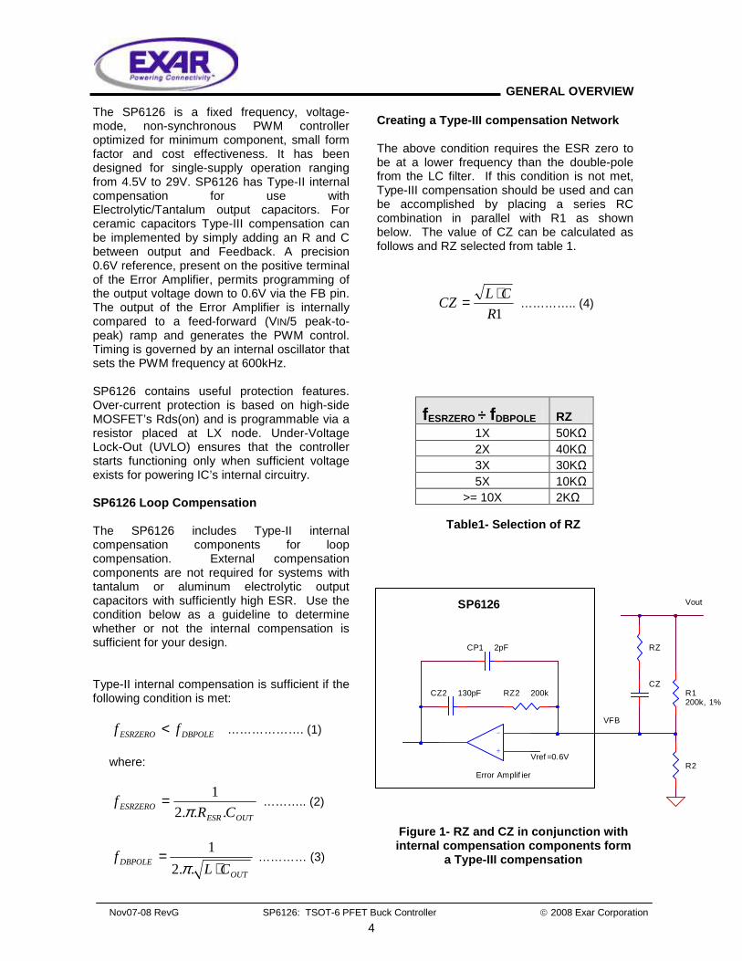
Creating a Type-III compensation Network The above condition requires the ESR zero to be at a lower frequency than the double-pole from the LC filter. If this condition is not met, Type-III compensation should be used and can be accomplished by placing a series RC combination in parallel with R1 as shown below. The value of CZ can be calculated as follows and RZ selected from table 1.
1R
CLCZ
⋅= ………….. (4)
Table1- Selection of RZ
Figure 1- RZ and CZ in conjunction with internal compensation components form
a Type-III compensation
fESRZERO ÷ fDBPOLE RZ 1X 50KΩ 2X 40KΩ 3X 30KΩ 5X 10KΩ
>= 10X 2KΩ
R1200k, 1%
R2
SP6126
VFB
+
-
RZ2 200kCZ2 130pF
CP1 2pF
Error Amplif ier
Vref =0.6V
Vout
RZ
CZ
GENERAL OVERVIEW
Nov07-08 RevG SP6126: TSOT-6 PFET Buck Controller 2008 Exar Corporation
5
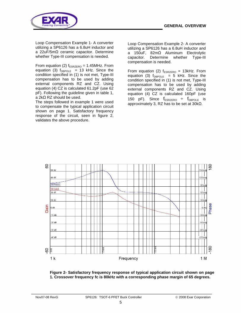
Loop Compensation Example 1- A converter utilizing a SP6126 has a 6.8uH inductor and a 22uF/5mΩ ceramic capacitor. Determine whether Type-III compensation is needed. From equation (2) fESRZERO = 1.45MHz. From equation (3) fDBPOLE = 13 kHz. Since the condition specified in (1) is not met, Type-III compensation has to be used by adding external components RZ and CZ. Using equation (4) CZ is calculated 61.2pF (use 62 pF). Following the guideline given in table 1, a 2kΩ RZ should be used. The steps followed in example 1 were used to compensate the typical application circuit shown on page 1. Satisfactory frequency response of the circuit, seen in figure 2, validates the above procedure.
Loop Compensation Example 2- A converter utilizing a SP6126 has a 6.8uH inductor and a 150uF, 82mΩ Aluminum Electrolytic capacitor. Determine whether Type-III compensation is needed. From equation (2) fESRZERO = 13kHz. From equation (3) fDBPOLE = 5 kHz. Since the condition specified in (1) is not met, Type-III compensation has to be used by adding external components RZ and CZ. Using equation (4) CZ is calculated 160pF (use 150 pF). Since fESRZERO ÷ fDBPOLE is approximately 3, RZ has to be set at 30kΩ.
Figure 2- Satisfactory frequency response of typical application circuit shown on page 1. Crossover frequency fc is 80kHz with a corresponding phase margin of 65 degrees.
GENERAL OVERVIEW
Nov07-08 RevG SP6126: TSOT-6 PFET Buck Controller 2008 Exar Corporation
6
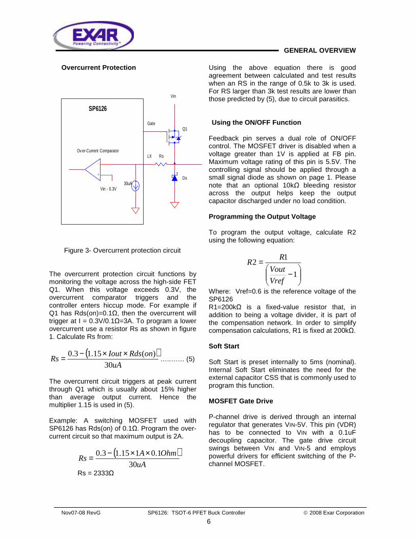
Overcurrent Protection
Ds
Q1
Rs
SP6126
Gate
LX
30uA
+
-
Vin - 0.3V
Vin
Ov er-Current Comparator
Figure 3- Overcurrent protection circuit
The overcurrent protection circuit functions by monitoring the voltage across the high-side FET Q1. When this voltage exceeds 0.3V, the overcurrent comparator triggers and the controller enters hiccup mode. For example if Q1 has Rds(on)=0.1Ω, then the overcurrent will trigger at I = 0.3V/0.1Ω=3A. To program a lower overcurrent use a resistor Rs as shown in figure 1. Calculate Rs from:
( )
uA
onRdsIoutRs
30)(15.13.0 ××−= …..…… (5)
The overcurrent circuit triggers at peak current through Q1 which is usually about 15% higher than average output current. Hence the multiplier 1.15 is used in (5). Example: A switching MOSFET used with SP6126 has Rds(on) of 0.1Ω. Program the over-current circuit so that maximum output is 2A.
( )uA
OhmARs
301.0115.13.0 ××−=
Rs = 2333Ω
Using the above equation there is good agreement between calculated and test results when an RS in the range of 0.5k to 3k is used. For RS larger than 3k test results are lower than those predicted by (5), due to circuit parasitics. Using the ON/OFF Function
Feedback pin serves a dual role of ON/OFF control. The MOSFET driver is disabled when a voltage greater than 1V is applied at FB pin. Maximum voltage rating of this pin is 5.5V. The controlling signal should be applied through a small signal diode as shown on page 1. Please note that an optional 10kΩ bleeding resistor across the output helps keep the output capacitor discharged under no load condition.
Programming the Output Voltage To program the output voltage, calculate R2 using the following equation:
−
=1
12
Vref
Vout
RR
Where: Vref=0.6 is the reference voltage of the SP6126 R1=200kΩ is a fixed-value resistor that, in addition to being a voltage divider, it is part of the compensation network. In order to simplify compensation calculations, R1 is fixed at 200kΩ.
Soft Start
Soft Start is preset internally to 5ms (nominal). Internal Soft Start eliminates the need for the external capacitor CSS that is commonly used to program this function.
MOSFET Gate Drive
P-channel drive is derived through an internal regulator that generates VIN-5V. This pin (VDR) has to be connected to VIN with a 0.1uF decoupling capacitor. The gate drive circuit swings between VIN and VIN-5 and employs powerful drivers for efficient switching of the P-channel MOSFET.
GENERAL OVERVIEW
Nov07-08 RevG SP6126: TSOT-6 PFET Buck Controller 2008 Exar Corporation
7
Power MOSFET Selection Select the Power MOSFET for Voltage rating BVDSS, On resistance RDS(ON), and thermal resistance Rthja. BVDSS should be about twice as high as VIN in order to guard against switching transients. Recommended MOSFET voltage rating for VIN of 5V, 12V and 24V is 12V, 30V and 40V respectively. RDS(ON) has to be selected such that when operating at peak current and junction temperature the Overcurrent threshold of the SP6126 is not exceeded. Allowing 50% for temperature coefficient of RDS(ON) and 15% for inductor current ripple, the following expression can be used:
××≤
Iout
mVONRDS
15.15.1
300)(
Within this constraint, selecting MOSFETs with lower RDS(ON) will reduce conduction losses at the expense of increased switching losses. As a rule of thumb select the highest RDS(ON) MOSFET that meets the above criteria. Switching losses can be assumed to roughly equal the conduction losses. A simplified expression for conduction losses is given by:
××=Vin
VoutONRDSIoutPcond )(
MOSFET’s junction temperature can be estimated from:
( ) TambientRthjaPcT +××= 2 Schottky Rectifier selection Select the Schottky for Voltage rating VR, Forward voltage Vf, and thermal resistance Rthja. Voltage rating should be selected using the same guidelines outlined for MOSFET voltage selection. For a low duty cycle application such as the circuit shown on first page, the Schottky is conducting most of the time and its conduction losses are the largest component of losses in the converter. Conduction losses can be estimated from:
−××=Vin
VoutIoutVfPc 1
where: Vf is diode forward voltage at IOUT Schottky’s AC losses due to its switching capacitance are negligible. Inductor Selection Select the Inductor for inductance L and saturation current ISAT. Select an inductor with ISAT higher than the programmed overcurrent. Calculate inductance from:
( )
×
×
×−=IripfVin
VoutVoutVinL
11
where: VIN is converter input voltage VOUT is converter output voltage f is switching frequency IRIP is inductor peak-to-peak current ripple (nominally set to 30% of IOUT) Keep in mind that a higher IRIP results in a smaller inductor which has the advantages of small size, low DC equivalent resistance DCR, high saturation current ISAT and allows the use of a lower output capacitance to meet a given step load transient. A higher IRIP, however, increases the output voltage ripple and increases the current at which converter enters Discontinuous Conduction Mode. The output current at which converter enters DCM is ½ of IRIP. Note that a negative current step load that drives the converter into DCM will result in a large output voltage transient. Therefore the lowest current for a step load should be larger than ½ of IRIP. Output Capacitor Selection Select the output capacitor for voltage rating, capacitance and Equivalent Series Resistance (ESR). Nominally the voltage rating is selected to be twice as large as the output voltage. Select the capacitance to satisfy the specification for output voltage overshoot/undershoot caused by current step load. A steady-state output current IOUT corresponds to inductor stored energy of ½ L IOUT
2.
GENERAL OVERVIEW
Nov07-08 RevG SP6126: TSOT-6 PFET Buck Controller 2008 Exar Corporation
8
A sudden decrease in IOUT forces the energy surplus in L to be absorbed by COUT. This causes an overshoot in output voltage that is corrected by power switch reduced duty cycle. Use the following equation to calculate COUT:
−×=
22
21
22
Vout-Vos
IILCout
Where: L is the output inductance I2 is the step load high current I1 is the step load low current Vos is output voltage including overshoot VOUT is steady state output voltage Output voltage undershoot calculation is more complicated. Test results for SP6126 buck circuits show that undershoot is approximately equal to overshoot. Therefore above equation provides a satisfactory method for calculating COUT. Select ESR such that output voltage ripple (VRIP) specification is met. There are two components to VRIP: First component arises from charge transferred to and from COUT during each cycle. The second component of VRIP is due to inductor ripple current flowing through output capacitor’s ESR. It can be calculated from:
2
2
8
1
××+×=
fsCoutESRIripVrip
Where: IRIP is inductor ripple current fs is switching frequency COUT is output capacitor calculated above Note that a smaller inductor results in a higher IRIP, therefore requiring a larger COUT and/or lower ESR in order to meet VRIP.
Input Capacitor Selection Select the input capacitor for Voltage, Capacitance, ripple current, ESR and ESL. Voltage rating is nominally selected to be twice the input voltage. The RMS value of input capacitor current, assuming a low inductor ripple current (IRIP), can be calculated from:
( )DDIoutIcin −×= 1
In general total input voltage ripple should be kept below 1.5% of VIN (not to exceed 180mV). Input voltage ripple has three components: ESR and ESL cause a step voltage drop upon turn on of the MOSFET. During on time capacitor discharges linearly as it supplies IOUT-Iin. The contribution to Input voltage ripple by each term can be calculated from:
( )2
,VinCinfs
VoutVinVoutIoutCinV
××−××=∆
( )IripIoutESRESRV 5.0, −=∆ ( )
Trise
IripIoutESLESLV
5.0,
−=∆
Where Trise is the rise time of current through capacitor Total input voltage ripple is sum of the above:
ESLVESRVCinVTotV ,,,, ∆+∆+∆=∆
GENERAL OVERVIEW
Nov07-08 RevG SP6126: TSOT-6 PFET Buck Controller 2008 Exar Corporation
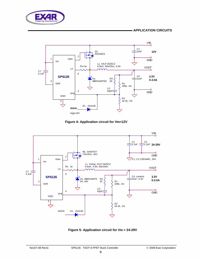
9
High=Of f
L1, IHLP-2525CZ6.8uH, 60mOhm, 4.5A
C422uFDs
MBRA340T3GR1200k, 1%
RZ2K
R244.2k, 1%
Q1Si2343DS
CZ62pF
C70.1uF
C110uF
Rs=1k
D1 1N4148
12V
SHDN
VIN
GND
GND
VOUT
Vin
GND
VDR
VFB
Gate
LX
SP6126 3.3V0-2.0A
5
3
12
6
4
Figure 4- Application circuit for VIN=12V
C22.2uF
C1, C2 CERAMIC, 50V
L1, Vishay IHLP-2525CZ6.8uH, 4.5A, 60mOhm
Ds, MBRA340T33A, 40V R1
200k, 1%
RZ2K
R244.2k, 1%
M1, Si4447DY72mOhm, 40V
CZ62pF
C70.1uF
Rs 1k
C4, ceramic22uF, 6.3V
D1 1N4148
24-29V
SHDN
GND
VIN
GND
VOUT
VDR
VFB
VinGate
LX
GND
SP6126 3.3V0-2.0A
1
5
3
2
6
4
C12.2uF
Figure 5- Application circuit for VIN = 24-29V
APPLICATION CIRCUITS

Nov07-08 RevG SP6126: TSOT-6 PFET Buck Controller 2008 Exar Corporation
10
TYPICAL PERFORMANCE CHARACTERISTICS
Figure 7- Efficiency at VIN = 12 V
Figure 6- Application circuit for VOUT = 4.5-5.5 V
High=Of f
L1, Vishay IHLP-2525CZ3.3uH, 6A, 30mOhm
Ds, MBRA340T33A, 40V R1
200k, 1%
RZ2K
R244.2k, 1%
M1, Si2335DS51mOhm, 12V
CZ33pF
C70.1uF
Rs 1k
C4, ceramic22uF, 6.3V
D1 1N4148
4.5-5.5 V
SHDN
GND
VIN
GND
VOUT
Vin
VDR
VFB
Gate
LX
GND
SP6126 3.3V0-3A
1
5
3
2
6
4
C110uF
C210uF
C310uF
SP6126 Efficiency versus Iout, Vin=12V,Ta=25C
60
70
80
90
100
0.0 0.5 1.0 1.5 2.0 2.5
Iout (A)
Effi
cien
cy (
%)
Vout=3.3V Vout=5V Vout=2.5V

Nov07-08 RevG SP6126: TSOT-6 PFET Buck Controller 2008 Exar Corporation
11
TYPICAL PERFORMANCE CHARACTERISTICS
SP6126 Efficiency versus Iout, Vin=24V,Ta=25C
50
60
70
80
90
0.0 0.5 1.0 1.5 2.0 2.5
Iout (A)
Effi
cien
cy (
%)
Vout=3.3V Vout=5V
Figure 8- Efficiency at VIN = 24 V
SP6126 Efficiency versus Iout, Vin=5V,Ta=25C
70
75
80
85
90
95
100
0.0 0.5 1.0 1.5 2.0 2.5 3.0
Iout (A)
Effi
cien
cy (
%)
Vout=2.5V Vout=3.3V
Figure 9- Efficiency at VIN = 5 V

Nov07-08 RevG SP6126: TSOT-6 PFET Buck Controller 2008 Exar Corporation
12
TYPICAL PERFORMANCE CHARACTERISTICS
Figure 10- Step load 1-2A, Figure 11- Step load 0.3-2A,
ch1: VIN; ch2: VOUT; ch3: IOUT ch1: VIN; ch2: VOUT; ch3: IOUT
Figure 12- Startup no load, Figure 13- Start up 2A,
ch1: VIN ch2: VOUT, ch3: IOUT ch1: VIN; ch2: VOUT; ch3: IOUT
Figure 14- Output ripple at 0A is 11mV, Figure 15- Output ripple at 2A is 18mV, ch1: VIN; ch2: VOUT; ch3: IOUT ch1: VIN; ch2: VOUT; ch3: IOUT
Nov07-08 RevG SP6126: TSOT-6 PFET Buck Controller 2008 Exar Corporation
13
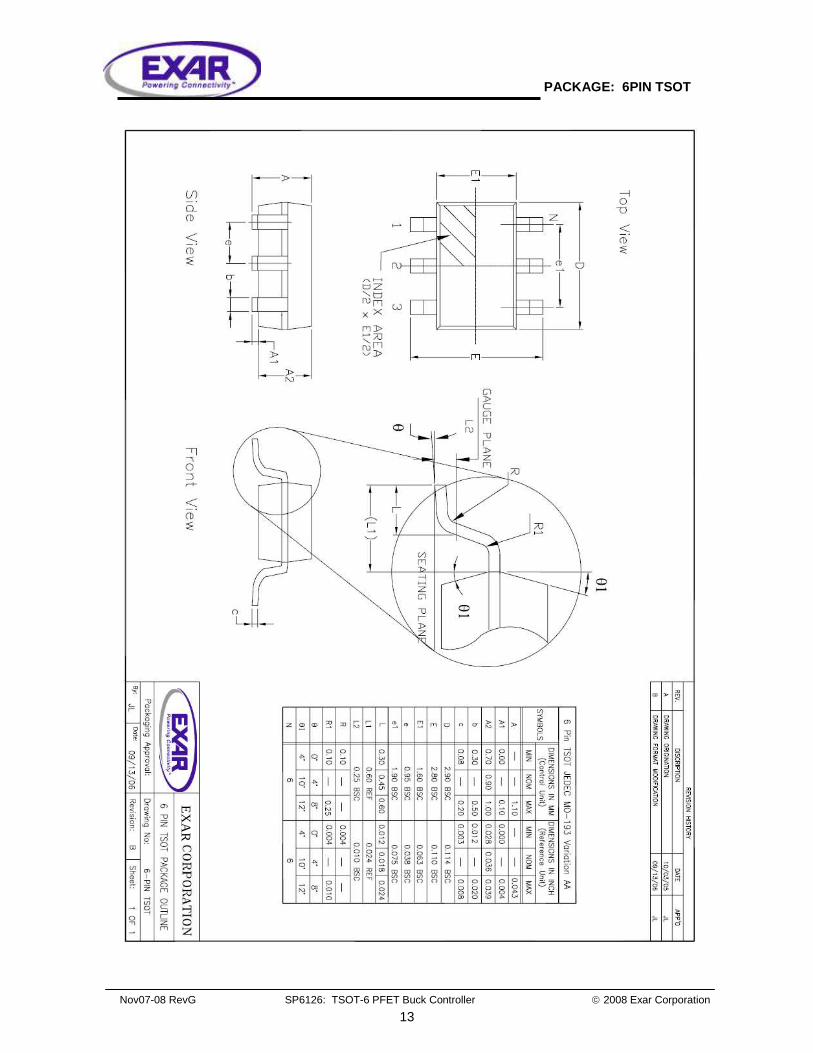
PACKAGE: 6PIN TS OT
EX
AR
Nov07-08 RevG SP6126: TSOT-6 PFET Buck Controller 2008 Exar Corporation
14
ORDERING INFORMATION
Part Number Temperature Range Package SP6126EK1-L………………………………….-40°C to +125°C…………….…(Lead Free) 6 Pin TSOT SP6126EK1-L/TR..…………………………....-40°C to +125°C….………...….(Lead Free) 6 Pin TSOT /TR = Tape and Reel Pack Quantity for Tape and Reel is 2500
For further assistance: Email: [email protected] EXAR Technical Documentation: http://www.exar.com/TechDoc/default.aspx?
Exar Corporation Headquarters and Sales Office 48720 Kato Road Fremont, CA 94538 main: 510-668-7000 fax: 510-668-7030
EXAR Corporation reserves the right to make changes to the products contained in this publication in order to improve design, performance or reliability. EXAR Corporation assumes no responsibility for the use of any circuits described herein, conveys no license under any patent or other right, and makes no representation that the circuits are free of patent infringement. Charts and schedules contained here in are only for illustration purposes and may vary depending upon a user’s specific application. While the information in this publication has been carefully checked; no responsibility, however, is assumed for inaccuracies. EXAR Corporation does not recommend the use of any of its products in life support applications where the failure or malfunction of the product can reasonably be expected to cause failure of the life support system or to significantly affect its safety or effectiveness. Products are not authorized for use in such applications unless EXAR Corporation receives, in writing, assurances to its satisfaction that: (a) the risk of injury or damage has been minimized; (b) the user assumes all such risks; (c) potential liability of EXAR Corporation is adequately protected under the circumstances.