high-speed serial i/o made simple -...
TRANSCRIPT

How Do You Get 10-Gbps I/O Performance?
High-speed serial I/O can be used to solve system interconnect design challenges. Such I/Os, when integrated into a highly programmable digital environment such as an FPGA, allow you to create high-performance designs that were never possible before. This book discusses the many aspects of high-speed serial designs with real world examples of how to implement working designs, including:
■ Basic I/O Concepts – Differential signaling, System Synchronous, and Source Synchronous design techniques.
■ Pros and Cons of different implemenations – How to evaluate the cost advantages, the reduced EMI, the maximum data flow, and so on.
■ SERDES Design – Basic theory, how to implement highly efficient serial to parallel channels, coding schemes, and so on.
■ Design Considerations – Standard and custom protocols, signal integrity, impedance, shielding, and so on.
■ Testing – Interpreting eye patterns, reducing jitter, interoperability considerations, bit error testers, and so on.
High-Speed Serial I/0 Made SimpleA Designers‘ Guide, with FPGA Applications
Xcell Publications help you solve design challenges, bringing you the awareness of the latest tools, devices, and technologies;knowledge on how to design most effectively; and the next steps for implementing working solutions. See all of our books,magazines, technical journals, solutions guides, and brochures at: www.xilinx.com/xcell
Edition 1.0April, 2005
Connectivity Solutions
High-Speed Serial I/OMade SimpleA Designers’ Guide, with FPGA Applications
R
by Abhijit Athavaleand Carl Christensen
Edition 1.0Connectivity Solutions
High-Speed Serial I/O Made Sim
ple – A Designers’ Guide, w
ith FPGA A
pplicationsEdition 1.0
PN 0402399

CONNECTIVITY SOLUTIONS: EDITION 1.0 PRELIMINARY INFORMATION
High-Speed Serial I/OMade Simple
A Designer’s Guide with FPGA Applications
by
Abhijit AthavaleMarketing Manager, Connectivity Solutions, Xilinx, Inc.
and
Carl ChristensenTechnical Marketing

HIGH-SPEED SERIAL I/O MADE SIMPLE •
• ii
© 2005 Xilinx, Inc. All rights reserved. XILINX, the Xilinx Logo, and other designated brands included hereinare trademarks of Xilinx, Inc. PowerPC is a trademark of IBM, Inc. All other trademarks are the property of theirrespective owners.
NOTICE OF DISCLAIMER: The information stated in this book is “Preliminary Information” and is not to beused for design purposes. Xilinx is providing this design, code, or information "as is." By providing thedesign, code, or information as one possible implementation of this feature, application, or standard, Xilinxmakes no representation that this implementation is free from any claims of infringement. You areresponsible for obtaining any rights you may require for your implementation. Xilinx expressly disclaimsany warranty whatsoever with respect to the adequacy of the implementation, including but not limited toany warranties or representations that this implementation is free from claims of infringement and anyimplied warranties of merchantability or fitness for a particular purpose.
All terms mentioned in this book are known to be trademarks or service marks and are the property of theirrespective owners. Use of a term in this book should not be regarded as affecting the validity of any trademark orservice mark.
All rights reserved. No part of this book may be reproduced, in any form or by any means, without written per-mission from the publisher.
For copies of this book, write to:
Xilinx Connectivity SolutionsProduct Solutions Marketing/Xilinx Worldwide Marketing
Dept. 2450, 2100 Logic Drive, San Jose, CA 95124Tel: 408.879.6889, Fax: 308.371.8283
Preliminary Edition 1.0April 2005PN0402399

PRELIMINARY INFORMATION • iii
AcknowledgementsWe would like to offer our deepest thanks to Paul Galloway and Craig Abramson. Without their constantmotivation, direction, and encouragement, we could not have completed this project.
We are also indebted to Ryan Carlson for his invaluable assistance in structuring the book, and to ChuckBerry for his great support and sales interface.
To a host of reviewers that included Matt DiPaolo, Mike Degerstrom, and Scott Davidson, we want to offerour gratitude. They kept us honest, accurate, and up to date.
To Babak Hedayati and Tim Erjavec for their unwavering support and encouragement
Finally, we offer special thanks to Ray Johnson. He fully supported our effort and placed his personal stampof approval on this book by providing the Forward.

HIGH-SPEED SERIAL I/O MADE SIMPLE •
• iv
TABLE OF CONTENTS
PRELIMINARY INFORMATION Xilinx • v
Acknowledgements . . . . . . . . . . . . . . . . . . . . . . . . . . . . . . . . . . . . . . . . . . . . . . . . . . . . . iii
ForewordAbout the Authors . . . . . . . . . . . . . . . . . . . . . . . . . . . . . . . . . . . . . . . . . . . . . . . . . . . . . vii
IntroductionI/O Performance Limitations . . . . . . . . . . . . . . . . . . . . . . . . . . . . . . . . . . . . . . . . . . . . . . .1
Digital Design Solutions for I/O . . . . . . . . . . . . . . . . . . . . . . . . . . . . . . . . . . . . . . . . . . . .1
Introducing Multi-Gigabit Serial . . . . . . . . . . . . . . . . . . . . . . . . . . . . . . . . . . . . . . . . . . .1
History of Digital Electronic Communication . . . . . . . . . . . . . . . . . . . . . . . . . . . . . . . . . .2
Basic I/O Concepts . . . . . . . . . . . . . . . . . . . . . . . . . . . . . . . . . . . . . . . . . . . . . . . . . . . . . .3Differential Signal . . . . . . . . . . . . . . . . . . . . . . . . . . . . . . . . . . . . . . . . . . . . . . . . .4System-Synchronous, Source-Synchronous, and Self-Synchronous . . . . . . . . . . . . . .5Parallel Transfers . . . . . . . . . . . . . . . . . . . . . . . . . . . . . . . . . . . . . . . . . . . . . . . . .10
Constant I/O Improvement . . . . . . . . . . . . . . . . . . . . . . . . . . . . . . . . . . . . . . . . . . . . . . .10
Why Do We Need Gigabit Serial I/O?Design Concerns . . . . . . . . . . . . . . . . . . . . . . . . . . . . . . . . . . . . . . . . . . . . . . . . . . . . . . .11
Gigabit Serial I/O Advantages. . . . . . . . . . . . . . . . . . . . . . . . . . . . . . . . . . . . . . . . . . . . .11Maximum Data Flow . . . . . . . . . . . . . . . . . . . . . . . . . . . . . . . . . . . . . . . . . . . . . .11Pin Count . . . . . . . . . . . . . . . . . . . . . . . . . . . . . . . . . . . . . . . . . . . . . . . . . . . . . .14Simultaneous Switching Outputs . . . . . . . . . . . . . . . . . . . . . . . . . . . . . . . . . . . . .15EMI . . . . . . . . . . . . . . . . . . . . . . . . . . . . . . . . . . . . . . . . . . . . . . . . . . . . . . . . . . .15Cost . . . . . . . . . . . . . . . . . . . . . . . . . . . . . . . . . . . . . . . . . . . . . . . . . . . . . . . . . . .15Predefined Protocols . . . . . . . . . . . . . . . . . . . . . . . . . . . . . . . . . . . . . . . . . . . . . .16
What are the Disadvantages?. . . . . . . . . . . . . . . . . . . . . . . . . . . . . . . . . . . . . . . . . . . . . .16
Where Will Gigabit I/O Be Used? . . . . . . . . . . . . . . . . . . . . . . . . . . . . . . . . . . . . . . . . .16Chip-to-Chip . . . . . . . . . . . . . . . . . . . . . . . . . . . . . . . . . . . . . . . . . . . . . . . . . . . .16Board-to-Board/Backplanes . . . . . . . . . . . . . . . . . . . . . . . . . . . . . . . . . . . . . . . . .17Box-to-Box . . . . . . . . . . . . . . . . . . . . . . . . . . . . . . . . . . . . . . . . . . . . . . . . . . . . .18
The Future of Multi-gigabit Designs. . . . . . . . . . . . . . . . . . . . . . . . . . . . . . . . . . . . . . . .18
TechnologyReal-World Serial I/O . . . . . . . . . . . . . . . . . . . . . . . . . . . . . . . . . . . . . . . . . . . . . . . . . . .19
Gigabit-Serial Implementations . . . . . . . . . . . . . . . . . . . . . . . . . . . . . . . . . . . . . . . . . . .19
SERDES . . . . . . . . . . . . . . . . . . . . . . . . . . . . . . . . . . . . . . . . . . . . . . . . . . . . . . . . . . . . .20History of SERDES and CDR . . . . . . . . . . . . . . . . . . . . . . . . . . . . . . . . . . . . . . .20Basic Theory of Operations and Generic Block Diagram . . . . . . . . . . . . . . . . . . .21Why Are They So Fast? . . . . . . . . . . . . . . . . . . . . . . . . . . . . . . . . . . . . . . . . . . . .23
Line Encoding Schemes . . . . . . . . . . . . . . . . . . . . . . . . . . . . . . . . . . . . . . . . . . . . . . . . . .25

HIGH-SPEED SERIAL I/O MADE SIMPLE •
vi • Xilinx
8b/10b Encoding/Decoding . . . . . . . . . . . . . . . . . . . . . . . . . . . . . . . . . . . . . . . . 26Running Disparity . . . . . . . . . . . . . . . . . . . . . . . . . . . . . . . . . . . . . . . . . . . . . . . 26Control Characters . . . . . . . . . . . . . . . . . . . . . . . . . . . . . . . . . . . . . . . . . . . . . . . 27Comma Detection. . . . . . . . . . . . . . . . . . . . . . . . . . . . . . . . . . . . . . . . . . . . . . . . 27Scrambling . . . . . . . . . . . . . . . . . . . . . . . . . . . . . . . . . . . . . . . . . . . . . . . . . . . . . 294b/5b 64b/66b . . . . . . . . . . . . . . . . . . . . . . . . . . . . . . . . . . . . . . . . . . . . . . . . . . 314b/5b 64b/66b Trade-Offs . . . . . . . . . . . . . . . . . . . . . . . . . . . . . . . . . . . . . . . . . 34
Introduction to Packets . . . . . . . . . . . . . . . . . . . . . . . . . . . . . . . . . . . . . . . . . . . . . . . . . 35
Reference Clocking Requirements . . . . . . . . . . . . . . . . . . . . . . . . . . . . . . . . . . . . . . . . . 36
Clock Correction . . . . . . . . . . . . . . . . . . . . . . . . . . . . . . . . . . . . . . . . . . . . . . . . . . . . . . 37
Receive and Transmit Buffers. . . . . . . . . . . . . . . . . . . . . . . . . . . . . . . . . . . . . . . . . . . . . 38
Channel Bonding . . . . . . . . . . . . . . . . . . . . . . . . . . . . . . . . . . . . . . . . . . . . . . . . . . . . . . 39
Physical Signaling . . . . . . . . . . . . . . . . . . . . . . . . . . . . . . . . . . . . . . . . . . . . . . . . . . . . . 40
Pre-Emphasis . . . . . . . . . . . . . . . . . . . . . . . . . . . . . . . . . . . . . . . . . . . . . . . . . . . . . . . . . 42
Differential Transmission Lines . . . . . . . . . . . . . . . . . . . . . . . . . . . . . . . . . . . . . . . . . . . 45
Line Equalization . . . . . . . . . . . . . . . . . . . . . . . . . . . . . . . . . . . . . . . . . . . . . . . . . . . . . . 47
Optical. . . . . . . . . . . . . . . . . . . . . . . . . . . . . . . . . . . . . . . . . . . . . . . . . . . . . . . . . . . . . . 51
Bit Error Rate . . . . . . . . . . . . . . . . . . . . . . . . . . . . . . . . . . . . . . . . . . . . . . . . . . . . . . . . 52
Realities of Testing . . . . . . . . . . . . . . . . . . . . . . . . . . . . . . . . . . . . . . . . . . . . . . . . . . . . 53CRC . . . . . . . . . . . . . . . . . . . . . . . . . . . . . . . . . . . . . . . . . . . . . . . . . . . . . . . . . . 53FEC Used in Some Applications . . . . . . . . . . . . . . . . . . . . . . . . . . . . . . . . . . . . . 54
SERDES Technology Facilitates I/O Design. . . . . . . . . . . . . . . . . . . . . . . . . . . . . . . . . . 55
Designing with Gigabit Serial I/OThe Challenges of Multi-Gigabit Transceiver Design . . . . . . . . . . . . . . . . . . . . . . . . . . . 57
Design Considerations and Choices You Can Use . . . . . . . . . . . . . . . . . . . . . . . . . . . . . . 57
Protocols . . . . . . . . . . . . . . . . . . . . . . . . . . . . . . . . . . . . . . . . . . . . . . . . . . . . . . . . . . . . 57Standard Protocols . . . . . . . . . . . . . . . . . . . . . . . . . . . . . . . . . . . . . . . . . . . . . . . 58Custom Protocols . . . . . . . . . . . . . . . . . . . . . . . . . . . . . . . . . . . . . . . . . . . . . . . . 62
Signal Integrity . . . . . . . . . . . . . . . . . . . . . . . . . . . . . . . . . . . . . . . . . . . . . . . . . . . . . . . 65
Impedance . . . . . . . . . . . . . . . . . . . . . . . . . . . . . . . . . . . . . . . . . . . . . . . . . . . . . . . . . . . 65
Power. . . . . . . . . . . . . . . . . . . . . . . . . . . . . . . . . . . . . . . . . . . . . . . . . . . . . . . . . . . . . . . 66
Shielding . . . . . . . . . . . . . . . . . . . . . . . . . . . . . . . . . . . . . . . . . . . . . . . . . . . . . . . . . . . . 73
Boards, Connectors, and Cables . . . . . . . . . . . . . . . . . . . . . . . . . . . . . . . . . . . . . . . . . . . 73Printed Circuit Board Design . . . . . . . . . . . . . . . . . . . . . . . . . . . . . . . . . . . . . . . 73
Connector Selection . . . . . . . . . . . . . . . . . . . . . . . . . . . . . . . . . . . . . . . . . . . . . . . . . . . . 79
Cable Selection. . . . . . . . . . . . . . . . . . . . . . . . . . . . . . . . . . . . . . . . . . . . . . . . . . . . . . . . 81
Simulation . . . . . . . . . . . . . . . . . . . . . . . . . . . . . . . . . . . . . . . . . . . . . . . . . . . . . . . . . . . 83Analog . . . . . . . . . . . . . . . . . . . . . . . . . . . . . . . . . . . . . . . . . . . . . . . . . . . . . . . . 83Digital . . . . . . . . . . . . . . . . . . . . . . . . . . . . . . . . . . . . . . . . . . . . . . . . . . . . . . . . 84

TABLE OF CONTENTS
PRELIMINARY INFORMATION Xilinx • vii
Test and Measurement . . . . . . . . . . . . . . . . . . . . . . . . . . . . . . . . . . . . . . . . . . . . . . . . . .86Sampling Oscilloscopes and Digital Communication Analyzers . . . . . . . . . . . . . .86Time Delay Reflectometer . . . . . . . . . . . . . . . . . . . . . . . . . . . . . . . . . . . . . . . . . .87Eye Patterns . . . . . . . . . . . . . . . . . . . . . . . . . . . . . . . . . . . . . . . . . . . . . . . . . . . . .89Jitter . . . . . . . . . . . . . . . . . . . . . . . . . . . . . . . . . . . . . . . . . . . . . . . . . . . . . . . . . .93Generators and Bit Error Testers . . . . . . . . . . . . . . . . . . . . . . . . . . . . . . . . . . . . .94Putting the Equipment to Use . . . . . . . . . . . . . . . . . . . . . . . . . . . . . . . . . . . . . . .96Multi-gigabit Debug Hints . . . . . . . . . . . . . . . . . . . . . . . . . . . . . . . . . . . . . . . . .97
Interoperability . . . . . . . . . . . . . . . . . . . . . . . . . . . . . . . . . . . . . . . . . . . . . . . . . . . . . . . .99Protocol Level . . . . . . . . . . . . . . . . . . . . . . . . . . . . . . . . . . . . . . . . . . . . . . . . . . .99
Electrical . . . . . . . . . . . . . . . . . . . . . . . . . . . . . . . . . . . . . . . . . . . . . . . . . . . . . . . . . . . .100
Other Resources . . . . . . . . . . . . . . . . . . . . . . . . . . . . . . . . . . . . . . . . . . . . . . . . . . . . . .100Design Services . . . . . . . . . . . . . . . . . . . . . . . . . . . . . . . . . . . . . . . . . . . . . . . . .100Testing Centers . . . . . . . . . . . . . . . . . . . . . . . . . . . . . . . . . . . . . . . . . . . . . . . . .100Development Platforms . . . . . . . . . . . . . . . . . . . . . . . . . . . . . . . . . . . . . . . . . . .101
Xilinx—Your Design PartnerSerial I/O Design Considerations . . . . . . . . . . . . . . . . . . . . . . . . . . . . . . . . . . . . . . . . . .103
One Stop Serial I/O Web Portal . . . . . . . . . . . . . . . . . . . . . . . . . . . . . . . . . . . . . . . . . .103
Signal Integrity Central. . . . . . . . . . . . . . . . . . . . . . . . . . . . . . . . . . . . . . . . . . . . . . . . .105
Additional References . . . . . . . . . . . . . . . . . . . . . . . . . . . . . . . . . . . . . . . . . . . . . . . . . .106
Xilinx—A Powerful Design Partner . . . . . . . . . . . . . . . . . . . . . . . . . . . . . . . . . . . . . . .107
World-Class Xilinx Support . . . . . . . . . . . . . . . . . . . . . . . . . . . . . . . . . . . . . . . . . . . . .108
Sample SERDES Data -- RocketIO X Transceiver OverviewBasic Architecture and Capabilities . . . . . . . . . . . . . . . . . . . . . . . . . . . . . . . . . . . . . . . .109
RocketIO X Transceiver Instantiations . . . . . . . . . . . . . . . . . . . . . . . . . . . . . . . . . . . . .112HDL Code Examples . . . . . . . . . . . . . . . . . . . . . . . . . . . . . . . . . . . . . . . . . . . . .112
Available Ports . . . . . . . . . . . . . . . . . . . . . . . . . . . . . . . . . . . . . . . . . . . . . . . . . . . . . . .113
Primitive Attributes . . . . . . . . . . . . . . . . . . . . . . . . . . . . . . . . . . . . . . . . . . . . . . . . . . .120
Modifiable Attributes . . . . . . . . . . . . . . . . . . . . . . . . . . . . . . . . . . . . . . . . . . . . . . . . . .126
Byte Mapping . . . . . . . . . . . . . . . . . . . . . . . . . . . . . . . . . . . . . . . . . . . . . . . . . . . . . . . .126
Digital Design Considerations. . . . . . . . . . . . . . . . . . . . . . . . . . . . . . . . . . . . . . . . . . . .127
Top-Level Architecture . . . . . . . . . . . . . . . . . . . . . . . . . . . . . . . . . . . . . . . . . . . . . . . . .128Transmit Architecture . . . . . . . . . . . . . . . . . . . . . . . . . . . . . . . . . . . . . . . . . . . .128Receive Architecture . . . . . . . . . . . . . . . . . . . . . . . . . . . . . . . . . . . . . . . . . . . . .129Operation Modes . . . . . . . . . . . . . . . . . . . . . . . . . . . . . . . . . . . . . . . . . . . . . . . .129
Block Level Functions . . . . . . . . . . . . . . . . . . . . . . . . . . . . . . . . . . . . . . . . . . . . . . . . . .130Classification of Signals and Overloading . . . . . . . . . . . . . . . . . . . . . . . . . . . . . .130
HIGH-SPEED SERIAL I/O MADE SIMPLE •
viii • Xilinx
Bus Interface. . . . . . . . . . . . . . . . . . . . . . . . . . . . . . . . . . . . . . . . . . . . . . . . . . . 1328b/10b . . . . . . . . . . . . . . . . . . . . . . . . . . . . . . . . . . . . . . . . . . . . . . . . . . . . . . . 133Vitesse Disparity Example . . . . . . . . . . . . . . . . . . . . . . . . . . . . . . . . . . . . . . . . 139Comma Detection. . . . . . . . . . . . . . . . . . . . . . . . . . . . . . . . . . . . . . . . . . . . . . . 14064b/66b . . . . . . . . . . . . . . . . . . . . . . . . . . . . . . . . . . . . . . . . . . . . . . . . . . . . . . 144Functions Common to All Protocols . . . . . . . . . . . . . . . . . . . . . . . . . . . . . . . . . 150Channel Bonding . . . . . . . . . . . . . . . . . . . . . . . . . . . . . . . . . . . . . . . . . . . . . . . 152Status and Event Bus . . . . . . . . . . . . . . . . . . . . . . . . . . . . . . . . . . . . . . . . . . . . 155
8b/10b TablesValid Data and Control Characters . . . . . . . . . . . . . . . . . . . . . . . . . . . . . . . . . . . . . . . . 161
A Comparison of Two DifferentFPGA-to-FPGA Data LinksAbstract . . . . . . . . . . . . . . . . . . . . . . . . . . . . . . . . . . . . . . . . . . . . . . . . . . . . . . . . . . . . 173
Introduction. . . . . . . . . . . . . . . . . . . . . . . . . . . . . . . . . . . . . . . . . . . . . . . . . . . . . . . . . 173
Requirements and System Architecture Concerns/Features . . . . . . . . . . . . . . . . . . . . . . 174The Slow Link . . . . . . . . . . . . . . . . . . . . . . . . . . . . . . . . . . . . . . . . . . . . . . . . . 174The Fast Link . . . . . . . . . . . . . . . . . . . . . . . . . . . . . . . . . . . . . . . . . . . . . . . . . . 174
Implementation Details . . . . . . . . . . . . . . . . . . . . . . . . . . . . . . . . . . . . . . . . . . . . . . . . 177The Slow Link . . . . . . . . . . . . . . . . . . . . . . . . . . . . . . . . . . . . . . . . . . . . . . . . . 177The Fast Link . . . . . . . . . . . . . . . . . . . . . . . . . . . . . . . . . . . . . . . . . . . . . . . . . . 177
Proving Our Concept . . . . . . . . . . . . . . . . . . . . . . . . . . . . . . . . . . . . . . . . . . . . . . . . . . 178Testing the Slow Link. . . . . . . . . . . . . . . . . . . . . . . . . . . . . . . . . . . . . . . . . . . . 178Testing the Fast Link . . . . . . . . . . . . . . . . . . . . . . . . . . . . . . . . . . . . . . . . . . . . 182
Conclusion . . . . . . . . . . . . . . . . . . . . . . . . . . . . . . . . . . . . . . . . . . . . . . . . . . . . . . . . . . 186
Acknowledgements . . . . . . . . . . . . . . . . . . . . . . . . . . . . . . . . . . . . . . . . . . . . . . . . . . . 186
Glossary
PRELIMINARY INFORMATION Xilinx • v
Foreword
“An invasion of armies can be resisted, but not an idea whose time has come.”
- Victor Hugo (1802 –1885) 'Histoire d'un crime,' 1852
There are only a handful of occasions in life when we are fortunate enough to be part of a new dis-covery or an idea whose time has finally come. Some of these ideas or innovations can drastically change the universe we live in. Think of how it must have felt to be in the National Institutes of Health lab when bio-scientists put the finishing touches on mapping the entire human genome—identifying the last gene in our DNA structure. Or at Bell Labs when Bardeen, Brattain, and Shockley demonstrated the first working transistor that led to a communications revolution.
In just the last 50 years, scientists and engineers have produced an astonishing number and vari-ety of scientific and technological breakthroughs. They formulated ideas that changed the way we think and the way we do almost everything. For example, the desire to link research center computers evolved into today’s Internet—an innovation many believe to be the most important instrument of business, social, and political change created in our lifetime.
Today we are again in a position to be both witness and participant in one of these rare technolog-ical moments. A fundamental shift is occurring in the electronics industry⎯a shift from parallel I/O schemes to serial I/O connectivity solutions. This change is driven by companies across a wide-range of industries as a means to reduce system costs, simplify system design, and provide the scalability needed to meet new bandwidth requirements.
At Xilinx, we firmly believe that serial connectivity solutions will ultimately be deployed in nearly every aspect of every electronic product imaginable. This deployment will appear in chip-to-chip interfaces, backplane connectivity and system boards, and box-to-box communications, to name a few. In support of this belief, we announced a ”High-Speed Serial Initiative” to help accelerate the industry move from parallel to high-speed serial I/O. This initiative includes delivering a new gener-ation of connectivity solutions for system designs that meet bandwidth requirements from 622 mega-bits per second (Mb/s) to 11.1 gigabits per second (Gb/s), and beyond.
Industry analysts agree that the High-Speed Serial Initiative is inevitable because parallel I/O schemes reach physical limitations when data rates begin to exceed just 1 Gb/s and can no longer pro-vide a reliable, cost-effective means for keeping signals synchronized. Serial I/O-based designs offer many advantages over traditional parallel implementations including fewer device pins, reduced board space requirements, fewer printed circuit board (PCB) layers, easier layout of the PCB, smaller connec-tors, lower electromagnetic interference, and better noise immunity.
This shift from parallel to serial will not be without engineering challenges. Among these, the biggest is the perception that designing high-speed serial I/O solutions is so difficult and complex that system engineers would rather continue using existing parallel technologies in spite of significant dis-advantages. To address these challenges, we created the Serial I/O Starter Guide. It provides assistance to all designers who are intrigued by the rapidly advancing serial technology but are hesitant to take that first step. For those readers that have already designed with serial, this book can be viewed as an in-depth refresher course.

HIGH-SPEED SERIAL I/O MADE SIMPLE •
vi • Xilinx Preliminary Information
Through the High-Speed Serial Initiative, Xilinx is providing both technical expertise and com-plete, pre-engineered solutions for a wide range of serial system architectures. These architectures include networking, telecommunications, and enterprise storage markets served by Xilinx Platform FPGAs with integrated serial I/O transceivers—the ultimate connectivity platform.
In addition to this book, Xilinx remains an active participant in key industry organizations help-ing to drive serial technology standards. In addition, Xilinx offers an extensive network of "ecosystem" partners (EDA, reference design, IP, design services, etc.) to guarantee interoperability and access to the latest technology, techniques, and design tools.
The world is embracing serial technology. The inclusion of high-speed serial I/O such as Rocke-tIO™ transceivers in an FPGA has made serial the preferred system connectivity solution. We also recognize that many of the challenges of high-speed serial design are still new for most designers knowledgeable in parallel I/O technologies. The Serial I/O Starter Guide provides the fundamental principals of serial I/O design so that anyone can start to correctly apply this revolutionary technology.
Raymond R. Johnson, Vice President and General Manager, Xilinx, Communications Technology Division

FOREWORD
PRELIMINARY INFORMATION Xilinx • vii
About the AuthorsAbhijit Athavale
Abhijit Athavale is Marketing Manager of Connectivity Solutions at Xilinx. His responsibilities includedevelopment of strategy, product positioning, and marketing programs for the company's high-speed serialand parallel connectivity offerings. Since joining Xilinx in 1995, he has also held positions in marketing,applications, and software engineering. Previously, Athavale was an R&D engineer designing communica-tions products at Meltron. He received his Bachelor’s Degree in Electrical Engineering from the Universityof Pune in India and his Masters Degree in Electrical Engineering from Texas A&M University. He is anaccomplished speaker and author of several published papers.
Carl Christensen
Carl has been designing hardware and software for over 16 years. He is currently specializing in cutting-edge FPGA design and system architectures for Thomson (brand names include RCA, Technicolor, andGrass Valley).
Carl’s publications include technical papers at the Synopsys User Group Meetings (SNUG), the National Association of Broadcasters (NAB) convention, and Xilinx Expert User Symposium (XEUS). He currently has 16 patents/applications in review in the areas of forward error correction and broad-cast routing systems. With a BS EE from Utah State University and significant graduate level work in computer science, Carl has taught courses in HDL-based design and programming in industry and college settings.

HIGH-SPEED SERIAL I/O MADE SIMPLE •
viii • Xilinx Preliminary Information
PRELIMINARY INFORMATION XILINX • 1
CHAPTER 1
Introduction
An overview of digital I/O signal processing methods
I/O Performance LimitationsInput/output (I/O) has always played a crucial role in computer and industrial applications. But as sig-nal processing became more sophisticated, problems arose that prevented reliable I/O communication. In early parallel I/O buses, interface alignment problems prevented effective communication with out-side devices. And as higher speeds became prevalent in digital design, managing signal delays became problematic.
Digital Design Solutions for I/ODigital designers turned to a host of methods to increase signal speed and eliminate I/O problems. For example, differential signal processing was employed to increase speed in chip-to-chip communica-tions. And design methods such as signal-, source-, and self-synchronization refined inter-IC (inte-grated circuit) communication to provide reliable I/O at speeds demanded by the computer industry.
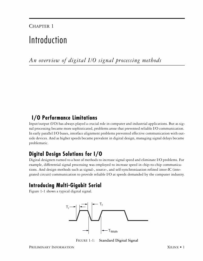
Introducing Multi-Gigabit SerialFigure 1-1 shows a typical digital signal.
FIGURE 1-1: Standard Digital Signal
TWidth
TfTr

HIGH-SPEED SERIAL I/O MADE SIMPLE •
2 • Xilinx PRELIMINARY INFORMATION
Notice the values of the time measurements listed on the diagram:
TR = 20 ps
TF = 20 ps
TWIDTH = 0.10 ns
These values represent a very fast waveform. Figure 1-2 adds historical signals for reference to show just how fast this waveform is.
Most signals cannot even get through their rise times in five bit times of the signal. So why dis-cuss such a signal? Because it represents the hottest trend in digital I/O—multi-gigabit serial.
This type of signal is exploding onto the market. It’s finding applications in everything from local area network (LAN) equipment, to cutting edge medical imaging equipment, to advanced fighter jet technology. Multi-gigabit signals are quickly becoming key to the expanding information age. To learn about this fast-moving technological advancement, let’s review the history of I/O design.
History of Digital Electronic CommunicationTransistor-transistor logic (TTL) was once the premier design method. Discrete gate ICs would com-municate with each other to form larger circuits that were then integrated into complex ICs such as multi-bit registers and counters. Parallel communication dominated printed circuit board (PCB) assemblies for many years. But alignment problems were too difficult for outside communications. As a result, the serial port ruled box-to-box communications as evidenced by the serial printer ports in early computers.
Eventually the alignment problems were solved. High-speed parallel printer ports proliferated as parallel technologies evolved. These included Industry-Standard Architecture (ISA), Extended Indus-try-Standard Architecture (EISA) and Small Computer Systems Interface (SCSI), Peripheral Compo-nent Interconnect (PCI), and the smaller Personal Computer Memory Card Industry Association (PCMCIA).
Serial technology continued to coexist with parallel. Ethernet and Token Ring gained dominance in many applications. Eventually, Token Ring replaced Ethernet when it was made to work on cate-gory 5 (Cat 5) wire.
FIGURE 1-2: Adding Historical Signals
A critical part of learning about a new technology is learning the vocabulary. Throughout the book you will find def-initions of key terms set aside like this.
0.5 nsec
INTRODUCTION
PRELIMINARY INFORMATION XILINX • 3
Parallel technologies struggled to accommodate new interface demands. Standards like PCI 33 evolved into PCI 66 as more exotic signaling was required. For a while, low swing standards such as high-speed transistor logic (HSTL) attempted to support parallel technology. Meanwhile, Ethernet went from 10 Mb to 100 Mb to 1000 Mb per second. Such speeds made Ethernet highly desirable for the desktop.
About this time the fractional phase detector was introduced. This technology boosted serial interface speed to the multi-gigabit range. Serial was proving to be fast and strong and it found appli-cation as a backplane technology. As serial pin count and simultaneous switching outputs (SSO) improved, multi-gigabit serial gained prominence in PCB assemblies and replaced parallel.
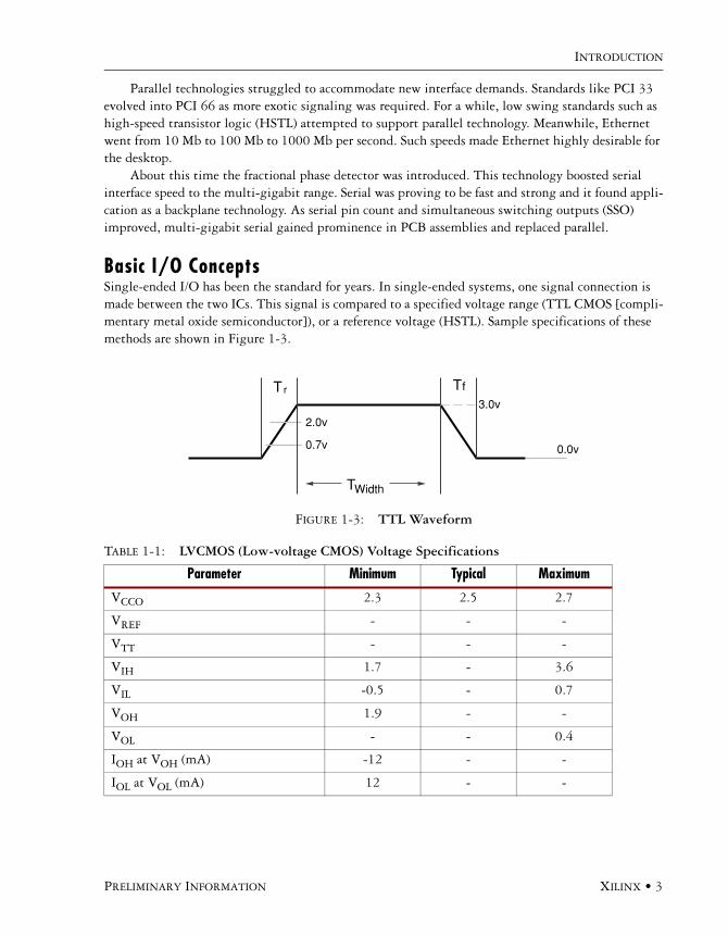
Basic I/O ConceptsSingle-ended I/O has been the standard for years. In single-ended systems, one signal connection is made between the two ICs. This signal is compared to a specified voltage range (TTL CMOS [compli-mentary metal oxide semiconductor]), or a reference voltage (HSTL). Sample specifications of these methods are shown in Figure 1-3.
FIGURE 1-3: TTL Waveform
TABLE 1-1: LVCMOS (Low-voltage CMOS) Voltage Specifications
Parameter Minimum Typical Maximum
VCCO 2.3 2.5 2.7
VREF - - -
VTT - - -
VIH 1.7 - 3.6
VIL -0.5 - 0.7
VOH 1.9 - -
VOL - - 0.4
IOH at VOH (mA) -12 - -
IOL at VOL (mA) 12 - -
2.0v
3.0v
0.7v 0.0v
Tr Tf
TWidth
HIGH-SPEED SERIAL I/O MADE SIMPLE •
4 • Xilinx PRELIMINARY INFORMATION
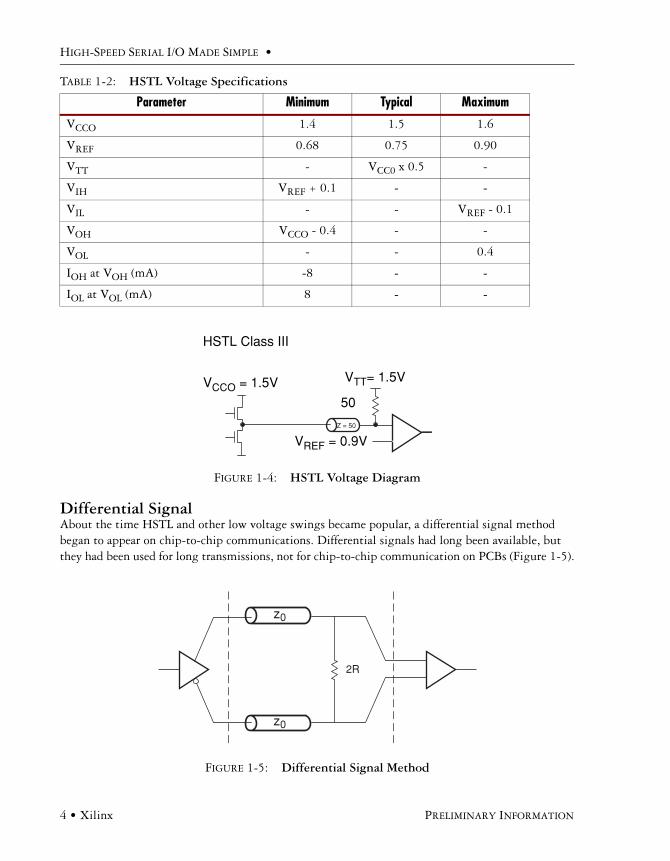
Differential SignalAbout the time HSTL and other low voltage swings became popular, a differential signal method began to appear on chip-to-chip communications. Differential signals had long been available, but they had been used for long transmissions, not for chip-to-chip communication on PCBs (Figure 1-5).
TABLE 1-2: HSTL Voltage Specifications
Parameter Minimum Typical Maximum
VCCO 1.4 1.5 1.6
VREF 0.68 0.75 0.90
VTT - VCC0 x 0.5 -
VIH VREF + 0.1 - -
VIL - - VREF - 0.1
VOH VCCO - 0.4 - -
VOL - - 0.4
IOH at VOH (mA) -8 - -
IOL at VOL (mA) 8 - -
FIGURE 1-4: HSTL Voltage Diagram
FIGURE 1-5: Differential Signal Method
VREF = 0.9V
VTT= 1.5V
50
VCCO = 1.5V
Z = 50
HSTL Class III
z0
z0
2R
INTRODUCTION
PRELIMINARY INFORMATION XILINX • 5
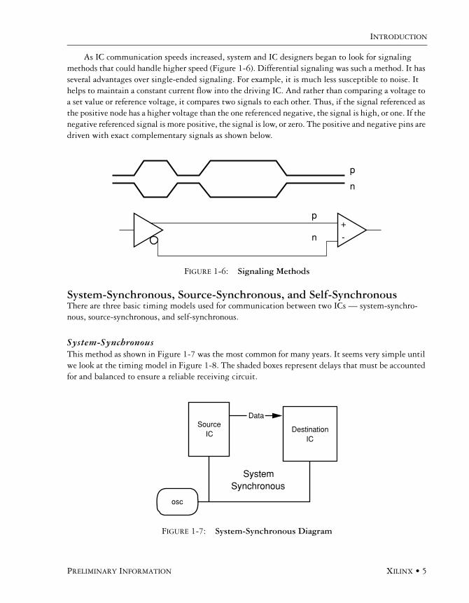
As IC communication speeds increased, system and IC designers began to look for signaling methods that could handle higher speed (Figure 1-6). Differential signaling was such a method. It has several advantages over single-ended signaling. For example, it is much less susceptible to noise. It helps to maintain a constant current flow into the driving IC. And rather than comparing a voltage to a set value or reference voltage, it compares two signals to each other. Thus, if the signal referenced as the positive node has a higher voltage than the one referenced negative, the signal is high, or one. If the negative referenced signal is more positive, the signal is low, or zero. The positive and negative pins are driven with exact complementary signals as shown below.
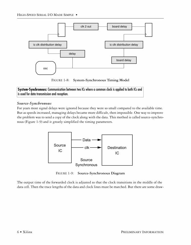
System-Synchronous, Source-Synchronous, and Self-SynchronousThere are three basic timing models used for communication between two ICs — system-synchro-nous, source-synchronous, and self-synchronous.
System-SynchronousThis method as shown in Figure 1-7 was the most common for many years. It seems very simple until we look at the timing model in Figure 1-8. The shaded boxes represent delays that must be accounted for and balanced to ensure a reliable receiving circuit.
FIGURE 1-6: Signaling Methods
FIGURE 1-7: System-Synchronous Diagram
p
n
+
-
p
n
SourceIC
osc
DestinationIC
Data
SystemSynchronous
HIGH-SPEED SERIAL I/O MADE SIMPLE •
6 • Xilinx PRELIMINARY INFORMATION
Source-SynchronousFor years most signal delays were ignored because they were so small compared to the available time. But as speeds increased, managing delays became more difficult, then impossible. One way to improve the problem was to send a copy of the clock along with the data. This method is called source-synchro-nous (Figure 1-9) and it greatly simplified the timing parameters.
The output time of the forwarded clock is adjusted so that the clock transitions in the middle of the data cell. Then the trace lengths of the data and clock lines must be matched. But there are some draw-
FIGURE 1-8: System-Synchronous Timing Model
System-Synchronous: Communication between two ICs where a common clock is applied to both ICs and is used for data transmission and reception.
FIGURE 1-9: Source-Synchronous Diagram
osc
clk 2 out
delay
board delay
board delay
ic clk distribution delay ic clk distribution delay
SourceIC
DestinationIC
Data
SourceSynchronous
clk

INTRODUCTION
PRELIMINARY INFORMATION XILINX • 7
backs. The received data on the destination IC must be moved from the received clock domain to a global IC clock.
Source-synchronous design results in a marked increase in the number of clock domains. This introduces timing constraint and analysis complications for devices such as a Field Programmable Gate Array (FPGA) with limited clock buffers, and an Application-Specific Integrated Circuit (ASIC) where each clock tree must be custom designed. The problem is aggravated on large parallel buses where board design limitations often force the use of more than one forwarded clock per data bus. Hence, a 32-bit bus may require four, or even eight forwarded clocks.
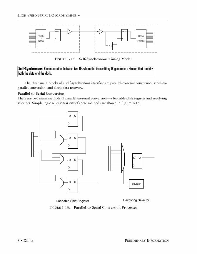
Self-SynchronousThe self-synchronous model is shown in Figure 1-11. Here, the data stream contains both the data and the clock.
FIGURE 1-10: Source-Synchronous Timing Model
Source-Synchronous: Communication between two ICs where the transmitting IC generates a clock that accompanies the data. The receiving IC uses this forwarded clock for data reception.
Clock Forwarded: Another term for source-synchronous.
FIGURE 1-11: Self-Synchronous Diagram
clk 2 out board delay
output delay board delay
buf
SourceIC
DestinationIC
Clk andData
SelfSynchronous
HIGH-SPEED SERIAL I/O MADE SIMPLE •
8 • Xilinx PRELIMINARY INFORMATION
The three main blocks of a self-synchronous interface are parallel-to-serial conversion, serial-to-parallel conversion, and clock data recovery.
Parallel-to-Serial ConversionThere are two main methods of parallel-to-serial conversion—a loadable shift register and revolving selectors. Simple logic representations of these methods are shown in Figure 1-13.
FIGURE 1-12: Self-Synchronous Timing Model
Self-Synchronous: Communication between two ICs where the transmitting IC generates a stream that contains both the data and the clock.
FIGURE 1-13: Parallel-to-Serial Conversion Processes
PLL
D0 Q
Serial2
Parallel
Parallel2
Serial
D0 Q
D Q
D Q
D Q
D Q
D Qcounter
Loadable Shift Register Revolving Selector

INTRODUCTION
PRELIMINARY INFORMATION XILINX • 9
Serial-to-Parallel Conversion
The serial-to-parallel process is just the opposite as shown in Figure 1-14.
Clock/Data Recovery
The clock recovery process (Figure 1-15) does not provide a common clock or send the clock with the data. Instead, a phased locked loop (PLL) is used to synthesizes a clock that matches the frequency of the clock that generates the incoming serial data stream.
FIGURE 1-14: Serial-to-Parallel Conversion Processes
FIGURE 1-15: Clock/Data Recovery Waveform
PLL: A phased locked loop is a circuit that takes a reference clock and an incoming signal and creates a new clock that is locked to the incoming signal.
D Q
D Q
D Q
D QWalking
One
Shift Register Revolving Enables
D Qen
D Qen
D Qen
D Qen
RCLK
RX_internal
RX_pin

HIGH-SPEED SERIAL I/O MADE SIMPLE •
10 • Xilinx PRELIMINARY INFORMATION
Parallel TransfersIn parallel transfers, additional control lines are often used to give different meanings to the data. Examples include data enables and multiplexing both data and control data onto the same bus.
In the serial domain, flags or markers are created to set data apart from non-data that is normally referred to as idle. Flags can also be used to mark different types of information such as data and con-trol.
Constant I/O ImprovementIndustrial requirements for bandwidth and speed have demanded constant improvements in I/O design. As parallel and serial I/O have fought for prominence in chip and device communication, both have benefited from design methods that yielded vastly increased speeds. The use of digital design methods such as differential and synchronous signal processing and parallel transfers have ensured con-tinued improvement in I/O performance for home and industry.
FIGURE 1-16: Parallel Transfer Example
FIGURE 1-17: Serial Domain Transfers Example
clk
data
enable
clk
data
enable
ctrl_not_data
idle df data if idle ifdf data idle
idle df data if idle ifcf control idle
df
cf
if
Data Flag marks start of data
Control Flag marks start of control
Idle Flag marks end of valid data and control

PRELIMINARY INFORMATION XILINX • 11
CHAPTER 2
Why Do We Need Gigabit Serial I/O?
A review of gigabit serial I/O design advantages
Design ConcernsThe average design engineer is in a quandary. He would like to stick with tried-and-true solutions because they offer predictability and dependability. But he must also strive for performance improve-ments in parameters such as data flow, pin count, electromagnetic interference (EMI), cost, and back-plane efficiency. Should he consider gigabit serial input/output (I/O)?
Gigabit Serial I/O AdvantagesWhat is the chief advantage of gigabit serial I/O? Speed. For getting data on and off of chips, boards, or boxes, nothing beats a high-speed serial link. With wire speeds from 1 to 12 Gb/s and payloads from 0.8 to 10Gb, that is a lot of data transfer. And with fewer pins, no massive simultaneous switch-ing output (SSO) problems, lower EMI, and lower cost, high-speed serial is the clear choice. Multi-gigabit transceivers (MGTs) are the way to go when we need to move lots of data fast. Let’s examine some of the advantages of gigabit serial I/O.
Maximum Data FlowSome large programmable logic devices have 20 or more 10-Gb serial transceivers for a total band-width of 200 Gb/s in and out. While that is an extreme, let's look at an example application that shows us how serial I/O speed can help system architects, board designers, and logic designers.
MGT: Multi-Gigabit Transceiver—Another name for multi-gigabit Serializer/Deserializer (SERDES). Receives par-allel data and allows transportation of high bandwidth data over a serial link.
HIGH-SPEED SERIAL I/O MADE SIMPLE •
12 • Xilinx PRELIMINARY INFORMATION
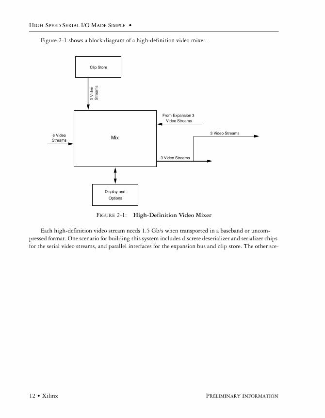
Figure 2-1 shows a block diagram of a high-definition video mixer.
Each high-definition video stream needs 1.5 Gb/s when transported in a baseband or uncom-pressed format. One scenario for building this system includes discrete deserializer and serializer chips for the serial video streams, and parallel interfaces for the expansion bus and clip store. The other sce-
FIGURE 2-1: High-Definition Video Mixer
Clip Store
Mix6 VideoStreams
From Expansion 3Video Streams
3 Video Streams
3 Video Streams
Display and
Options
3 V
ideo
Str
eam
s

WHY DO WE NEED GIGABIT SERIAL I/O?
PRELIMINARY INFORMATION XILINX • 13
nario uses gigabit transceivers inside the logic part to decode and encode the serial streams. The faster serial stream acts as the interface to the expansion connector and clip store.
FIGURE 2-2: Using Deserializer/Serializer Chips (Parallel)
Clip Store
expansionconnector
MixFPGA
60bits/75Mhz
SmallLCD
DisplayControl LEDs
20bits/75Mhz1bit/1.5Ghz Deserializer
20bits/75Mhz1bit/1.5Ghz Deserializer
20bits/75Mhz1bit/1.5Ghz Deserializer
20bits/75Mhz1bit/1.5Ghz Deserializer
20bits/75Mhz1bit/1.5Ghz Deserializer
20bits/75Mhz1bit/1.5Ghz Deserializer
20bi
ts/7
5Mhz
20bi
ts/7
5Mhz
20bi
ts/7
5Mhz
60bits/75Mhz
20bits/75Mhz 1bit/1.5GhzSerializer
20bits/75Mhz 1bit/1.5GhzSerializer
20bits/75Mhz 1bit/1.5GhzSerializer

HIGH-SPEED SERIAL I/O MADE SIMPLE •
14 • Xilinx PRELIMINARY INFORMATION
Pin CountPin count is the first problem encountered when trying to move a lot of data in and out of a chip or a board. The number of input and output pins is always limited. Although pin count tends to increase over time, it is never enough to keep up.
FIGURE 2-3: Using Gigabit Transceivers (Serial)
Clip Store
expansion
connector
Mix
FPGA
Small
LCD
DisplayControl LEDs
1Bit/4.5Ghz1bit/1.5Ghz
1Bit/
4.5G
hz
1bit/1.5Ghz
1bit/1.5Ghz
1bit/1.5Ghz
1bit/1.5Ghz
1bit/1.5Ghz
1bit/1.5Ghz
1bit/1.5Ghz
1bit/1.5Ghz
1Bit/4.5Ghz
WHY DO WE NEED GIGABIT SERIAL I/O?
PRELIMINARY INFORMATION XILINX • 15
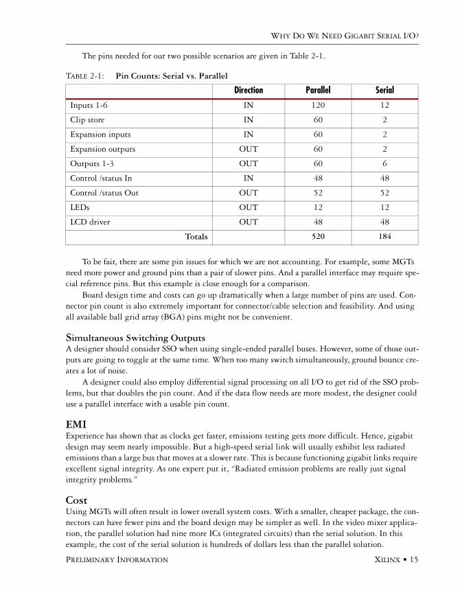
The pins needed for our two possible scenarios are given in Table 2-1.
To be fair, there are some pin issues for which we are not accounting. For example, some MGTs need more power and ground pins than a pair of slower pins. And a parallel interface may require spe-cial reference pins. But this example is close enough for a comparison.
Board design time and costs can go up dramatically when a large number of pins are used. Con-nector pin count is also extremely important for connector/cable selection and feasibility. And using all available ball grid array (BGA) pins might not be convenient.
Simultaneous Switching OutputsA designer should consider SSO when using single-ended parallel buses. However, some of those out-puts are going to toggle at the same time. When too many switch simultaneously, ground bounce cre-ates a lot of noise.
A designer could also employ differential signal processing on all I/O to get rid of the SSO prob-lems, but that doubles the pin count. And if the data flow needs are more modest, the designer could use a parallel interface with a usable pin count.
EMIExperience has shown that as clocks get faster, emissions testing gets more difficult. Hence, gigabit design may seem nearly impossible. But a high-speed serial link will usually exhibit less radiated emissions than a large bus that moves at a slower rate. This is because functioning gigabit links require excellent signal integrity. As one expert put it, “Radiated emission problems are really just signal integrity problems.”
CostUsing MGTs will often result in lower overall system costs. With a smaller, cheaper package, the con-nectors can have fewer pins and the board design may be simpler as well. In the video mixer applica-tion, the parallel solution had nine more ICs (integrated circuits) than the serial solution. In this example, the cost of the serial solution is hundreds of dollars less than the parallel solution.
TABLE 2-1: Pin Counts: Serial vs. Parallel
Direction Parallel Serial
Inputs 1-6 IN 120 12
Clip store IN 60 2
Expansion inputs IN 60 2
Expansion outputs OUT 60 2
Outputs 1-3 OUT 60 6
Control /status In IN 48 48
Control /status Out OUT 52 52
LEDs OUT 12 12
LCD driver OUT 48 48
Totals 520 184

HIGH-SPEED SERIAL I/O MADE SIMPLE •
16 • Xilinx PRELIMINARY INFORMATION
Predefined ProtocolsAnother benefit of using MGTs is the availability of predefined protocols and interface standards. From Aurora to XAUI, designs already exist for many different needs.
What are the Disadvantages?Before we think that gigabit serial I/O sounds too good to be true, let's look at the downsides. In our designs, we must first we must pay close attention to signal integrity issues. For example, one vendor reported a 90% failure rate on their first attempt with high-speed, multi-gigabit serial designs for a particular application. To improve the odds, we might need to perform analog simulations and use new, more complex bypassing schemes. In fact, we may even need to simulate and model the bypassing scheme.
We can also expect to pay more for impedance-controlled PC (printed circuit) boards, high-speed connectors, and cables. We will have to deal with complications and smaller time bases in digital sim-ulations. And when taking advantage of a predefined protocol, we must plan time for integration and extra gates or Central Processing Unit (CPU) cycles for protocol overhead.
Where Will Gigabit I/O Be Used?Initially, gigabit SERDES was confined to the telecommunications industry and to a few niche mar-kets such as broadcast video. Today, MGT applications appear in every section of the electronics indus-try — military, medical, networking, video, communications, etc. They are also being used on printed circuit board (PCB) assemblies through backplanes and between chassis. MGTs are critical to the future of electronics. Here is a sample of the industry standards that use multi-gigabit SERDES:
• FiberChannel (FC)• PCI Express• RapidIO Serial• Advanced Switching Interface• Serial ATA• 1-Gb Ethernet• 10-Gb Ethernet (XAUI)• Infiniband 1X, 4X, 12X
Chip-to-ChipSERDES was initially used to talk box-to-box. But it exploded into the marketplace because of how nicely it handles chip-to-chip communication on the same circuit board. Chip-to-chip communica-tion had previously been almost exclusively a parallel domain. The amount of logic needed to serialize and deserialize far outweighed any savings that come from pin count reduction.
But with deep sub-micron geometry, an incredible amount of logic can be achieved in a very small amount of silicon. SERDES can be included on parts for a very low silicon cost. Add to that the ever-increasing need for I/O bandwidth, and SERDES quickly becomes the logical choice for moving any significant amount of data chip-to-chip. Consider the following benefits of SERDES chip-to-chip communication:
• Pin Count: Smaller, cheaper packages.• Pin Count: Fewer layers on PCB assemblies.

WHY DO WE NEED GIGABIT SERIAL I/O?
PRELIMINARY INFORMATION XILINX • 17
• Smaller Packages: Smaller, cheaper boards and more compact designs.• SSO: Fewer pins and differential signaling eliminate the SSO problem.• Power: Usually a high-speed serial link will use less power than a parallel link. This is
especially true of some of the actively biased/terminated high-speed parallel standards like high-speed transistor logic (HSTL).
• Control Lines included: Often a parallel interface needs a few lines for control and enable in addition to the data lines. Serial links have enabling and control capabilities built into most protocols.
Board-to-Board/BackplanesAlthough they were once the best available, parallel architectures are at their limits. Most parallel bus protocols have evolved to the point where adding data bits is physically impractical because of pin counts on connectors. Clock skew, data skew, rise and fall times, and jitter limit the ability to increase clock frequency. Doubling the data rate can help, but it often requires moving to differential signal-ing, and that drastically increases pin count. Also, controlling the cross-talk issues on parallel buses is difficult.
New serial backplanes are somewhat different than parallel backplanes. They typically have ded-icated serial links from each node to every other node. Figure 2-4 illustrates the basic architecture of an old parallel bus and a new serial bus.
Serial bus architectures have a lot to offer. The pin count of a serial bus is a function of the number of nodes. For most practical node numbers, a serial architecture has fewer pins than the old parallel architectures.
FIGURE 2-4: Old Parallel Bus vs. New Serial Bus
1 2 3 4 5
60
1 2 3 4 5
4

HIGH-SPEED SERIAL I/O MADE SIMPLE •
18 • Xilinx PRELIMINARY INFORMATION
Perhaps the most important difference between the two is the bandwidth access method. In the parallel architectures, one node can transmit to one or many nodes. But while that node is transmit-ting, all other nodes are blocked. All nodes share the available bandwidth.
In serial buses, each node has a dedicated link to every other node. So one node can talk to one or to all nodes while another node is talking. In fact, all nodes can talk to all other nodes at the same time. Of course, the nodes will have to have First In First Out (FIFO) buffering and storage so they can pro-cess all the information being received.
Serial bus structure advantages include: • Higher bandwidth• Reduced pin count• Detected bandwidth node-to-node (no need to share)• Solutions are built into the SERDES• Easily supports protocols
Box-to-BoxWhile SERDES got their start connecting boxes, many designers do not consider multi-gigabit serial links for box-to-box communication. A common misconception is that box-to-box communication cannot be fast without using fiber optics. However, there are many links that go box-to-box for short distances over copper cabling systems. One standard that uses these links is Infiniband. The Infini-band spec allows for 1, 4, or 12 channels of serial data at 2.5 Gb/s per stream. The standard has been commercially available for a number of years and includes cables, connectors, and a protocol that are all well defined and tested.
The Future of Multi-gigabit DesignsAt first glance, multi-gigabit communication seems to impose unacceptable restrictions. Serial designers must contend with signal integrity, smaller time bases, and possibly the need for extra gates and additional CPU cycles. However, multi-gigabit advantages in box-to-box and chip-to-chip com-munication far outweigh the perceived shortcomings. For example, high speed, fewer pins, lower EMI, and lower cost make it the ideal choice in many communication designs. These advantages will ensure its continued use in communication applications far into the future.
FIGURE 2-5: Box-to-Box Connection
PRELIMINARY INFORMATION XILINX • 19
CHAPTER 3
Technology
Techniques for implementing gigabit-serial I/O
Real-World Serial I/OIn the previous chapters, we examined some of the challenges faced by input/output (I/O) designers. And we looked at some of the advantages serial I/O has to offer. But how does a design engineer actu-ally make use of serial I/O technology? Before design can begin, we need to know what’s available to help implement serial I/O solutions. We need to examine some serial building block devices to see if the tools are there for real-world implementation.
Gigabit-Serial ImplementationsIn this chapter we will look at some of the technologies involved with multi-gigabit links. We'll look at the Serializer/Deserializer (SERDES), its basic building blocks, and learn how all the speed is achieved (Figure 3-1). We will also review the format of the serial stream from both logical and phys-ical points of view. This information will give us a foundation for planning gigabit-serial I/O designs.

HIGH-SPEED SERIAL I/O MADE SIMPLE •
20 • Xilinx PRELIMINARY INFORMATION
SERDES
History of SERDES and CDRSerial-to-parallel and parallel-to-serial conversions have been a part of I/O design from the beginning. So has the idea of recovering a clock, or “locking a clock to an incoming stream.” So why has the SER-DES suddenly become so important?
As integrated circuit (IC) geometry grew smaller and maximum toggle rate (Fmax) increased, the need for I/O bandwidth exploded. In fact, some developments allowed for I/O frequency even faster than Fmax.
FIGURE 3-1: SERDES Block Diagram
Fmax: Maximum toggle rate of a flip-flop in a given technology or part.
Serializer
Deserializer
Clock
ManagerOSC
Encoding/
Decoding
Transmit and
Receiver
buffers/FIFO
Alignment
tx L
ine
inte
rfac
eR
x Li
nein
terf
ace

TECHNOLOGY
PRELIMINARY INFORMATION XILINX • 21
Basic Theory of Operations and Generic Block DiagramLet's look at the basic building blocks of a SERDES (Figure 3-2).
• Serializer: Takes n bits of parallel data changing at rate y and transforms them into a serial stream at a rate of n times y.
• Deserializer: Takes serial stream at a rate of n times y and changes it into parallel data of width n changing at rate y.
• Rx (Receive) Align: Aligns the incoming data into the proper word boundaries. Several different mechanisms can be used from automatic detection and alignment of a special reserved bit sequence (often called a comma) to user-controlled bit slips.
• Clock Manager: Manages various clocking needs including clock multiplication, clock division, and clock recovery.
• Transmit FIFO (First In First Out): Allows for storing of incoming data before transmission.
• Receive FIFO: Allows for storing of received data before removal; is essential in a system where clock correction is required.
• Receive Line Interface: Analog receive circuitry includes differential receiver and may include active or passive equalization.
• Transmit Line Interface: Analog transmission circuit often allows varying drive strengths. It may also allow for pre-emphasis of transitions.
• Line Encoder: Encodes the data into a more line-friendly format. This usually involves eliminating long sequences of non-changing bits. May also adjust data for an even balance of ones and zeros. (This is an optional block sometimes not included in a SERDES.)
• Line Decoder: Decodes from line encoded data to plain data. (This is an optional block that is sometimes done outside of the SERDES.)
• Clock Correction and Channel Bonding: Allows for correction of the difference between the transmit clock and the receive clock. Also allows for skew correction between multiple channels. (Channel bonding is optional and not always included in SERDES.)
FIGURE 3-2: SERDES Generic Block Diagram
SerializerLine
EncoderTransmit
FIFOtx L
ine
inte
rfac
e
DeserializerLine
decoderRX Elastic
BufferRX
Lin
eIn
terf
ace
ClockManagerOSC Clock Correction and
Channel Bonding
HIGH-SPEED SERIAL I/O MADE SIMPLE •
22 • Xilinx PRELIMINARY INFORMATION
Other possible functions can be included such as cyclic redundancy check (CRC) generators, CRC checkers, multiple encoding and decoding 4b/5b, 8b/10b, 64b/66b, settable scramblers, various alignment and daisy-chaining options, and clock configurable front and backends.
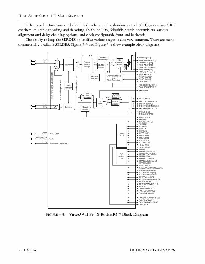
The ability to loop the SERDES on itself at various stages is also very common. There are many commercially-available SERDES. Figure 3-3 and Figure 3-4 show example block diagrams.
FIGURE 3-3: Virtex™-II Pro X RocketIO™ Block Diagram
Serializer
RXP
TXP
ClockManager
DeserializerCommaDetectRealign
8B/10B Decoder
TXFIFO
Channel Bondingand
Clock Correction CHBONDI[4:0]CHBONDO[4:0]
8B/10BEncoder
RXElasticBuffer
OutputPolarity
RXN
GNDA
TXN
RXRESET
RXCLKCORCNT[2:0]RXLOSSOFSYNC[1:0]
RXDATA[63:0]
RXNOTINTABLE[7:0]RXDISPERR[7:0]RXCHARISK[7:0]RXCHARISCOMMA[7:0]RXRUNDISP[7:0]RXBUFSTATUS[1:0]
ENCHANSYNC
RXUSRCLKRXUSRCLK2
CHBONDDONE
TXBUFERR
TXDATA[63:0]
TXBYPASS8B10B[7:0]TXCHARISK[7:0]TXCHARDISPMODE[7:0]TXCHARDISPVAL[7:0]
TXKERR[7:0]TXRUNDISP[7:0]
TXPOLARITYTXINHIBITLOOPBACK[1:0]TXRESET
REFCLKREFCLK2REFCLKSEL
TXUSRCLKTXUSRCLK2
VTTX
AVCCAUXRX
TX/RX GND
1.5V
Termination Supply TX
Pos
t Driv
er S
eria
l Loo
pbac
k P
ath
Par
alle
l Loo
pbac
k P
ath
BREFCLKPBREFCLKN
64B/66BBlock Sync
64B
/66B
Dec
oder
Gear Box
Scrambler
64B/66BEncoder
PMAAttribute
Load
PMAREGDATAIN[7:0]
RXCOMMADETUSERXDATAWIDTH[1:0]RXDECC64B66BUSE
PMAINITPMAREGADDR[5:0]
PMAREGRWPMAREGSTROBEPMARXLOCKSEL[1:0]PMARXLOCK
RXDEC8B10BUSERXDESCRAM64B66BUSE
REFCLKBSELRXBLCOKSYNC64B66BUSE
RXSLIDE
TXINTDATAWIDTH[1:0]TXSCRAM64B66BUSETXOUTCLK
RXIGNOREBTFRXINTDATAWIDTH[1:0]
TXDATAWIDTH[1:0]TXENC64B66BUSETXENC8B10BUSE
TXGEARBOX64B66BUSE
Pre
-Driv
er L
oopb
ack
Pat
h
64B/66BDescrambler
Clock / Reset

TECHNOLOGY
PRELIMINARY INFORMATION XILINX • 23
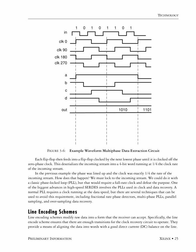
Why Are They So Fast?An unsettling aspect of the Gigabit SERDES is that they appear to be almost magical. They work with 3, 5, and even 10+ gigabits. How is that kind of speed possible? There are several techniques that pro-vide this speed.
A common element of most of these techniques is multiple phases (Figure 3-5 and Figure 3-6). We can get an idea of how multiple phases can help us by looking at a multiphase data extraction cir-cuit. If we have an incoming serial stream with a bit rate of x, we can recover the stream with a clock of x/4 by using multiple phases of the slow clock. The incoming stream is directed into four flip-flops, each running off a different phase of the clock (0, 90, 180, and 270).
FIGURE 3-4: Virtex-II Pro RocketIO Block Diagram
FPGA FABRICMULTI-GIGABIT TRANSCEIVER CORE
Serializer
RXP
TXP
ClockManager
Power Down
PACKAGEPINS
DeserializerCommaDetectRealign
8B/10B Decoder
TXFIFO
CRCCheck
CRC
Channel Bondingand
Clock Correction CHBONDI[3:0]CHBONDO[3:0]
8B/10BEncoder
RXElasticBuffer
OutputPolarity
RXN
GNDA
TXN
POWERDOWN
RXRECCLKRXPOLARITYRXREALIGNRXCOMMADET
RXRESET
RXCLKCORCNTRXLOSSOFSYNC
RXDATA[15:0]RXDATA[31:16]
RXCHECKINGCRCRXCRCERR
RXNOTINTABLE[3:0]RXDISPERR[3:0]RXCHARISK[3:0]RXCHARISCOMMA[3:0]RXRUNDISP[3:0]RXBUFSTATUS[1:0]
ENCHANSYNC
RXUSRCLKRXUSRCLK2
CHBONDDONE
TXBUFERR
TXDATA[15:0]TXDATA[31:16]
TXBYPASS8B10B[3:0]TXCHARISK[3:0]TXCHARDISPMODE[3:0]TXCHARDISPVAL[3:0]
TXKERR[3:0]TXRUNDISP[3:0]
TXPOLARITY
TXFORCECRCERR
TXINHIBIT
LOOPBACK[1:0]TXRESET
REFCLKREFCLK2REFCLKSEL
ENPCOMMAALIGNENMCOMMAALIGN
TXUSRCLKTXUSRCLK2
VTRX
AVCCAUXRX
VTTX
AVCCAUXTX
2.5V RX
TX/RX GND
Termination Supply RX
2.5V TX
Termination Supply TX
Ser
ial L
oopb
ack
Pat
h
Par
alle
l Loo
pbac
k P
ath
BREFCLKBREFCLK2

HIGH-SPEED SERIAL I/O MADE SIMPLE •
24 • Xilinx PRELIMINARY INFORMATION
FIGURE 3-5: Multiphase Data Extraction Circuit
D Q
D Q
D Q
D Q D Q D Q D Q
D Q D Q
D Q
D Q
d
c
b
a
090
270
180
IN
d3
d2
d1
d0
TECHNOLOGY
PRELIMINARY INFORMATION XILINX • 25
Each flip-flop then feeds into a flip-flop clocked by the next lowest phase until it is clocked off the zero-phase clock. This deserializes the incoming stream into a 4-bit word running at 1/4 the clock rate of the incoming stream.
In the previous example the phase was lined up and the clock was exactly 1/4 the rate of the incoming stream. How does that happen? We must lock to the incoming stream. We could do it with a classic phase-locked loop (PLL), but that would require a full-rate clock and defeat the purpose. One of the biggest advances in high-speed SERDES involves the PLLs used in clock and data recovery. A normal PLL requires a clock running at the data speed, but there are several techniques that can be used to avoid this requirement, including fractional rate phase detectors, multi-phase PLLs, parallel sampling, and over-sampling data recovery.
Line Encoding SchemesLine encoding schemes modify raw data into a form that the receiver can accept. Specifically, the line encode scheme ensures that there are enough transitions for the clock recovery circuit to operate. They provide a means of aligning the data into words with a good direct current (DC) balance on the line.
FIGURE 3-6: Example Waveform Multiphase Data Extraction Circuit
1010 1101
10 01 1 0 1 1
out
in
clk 0
d
clk 90
clk 180
clk 270
a
b
c
HIGH-SPEED SERIAL I/O MADE SIMPLE •
26 • Xilinx PRELIMINARY INFORMATION
Optionally, the line encoding scheme may also provide for implementation of clock correction, block synchronization and channel bonding, and division of the bandwidth into sub-channels.
There are two main line encoding schemes—value lookup schemes and self-modifying streams, or scramblers.
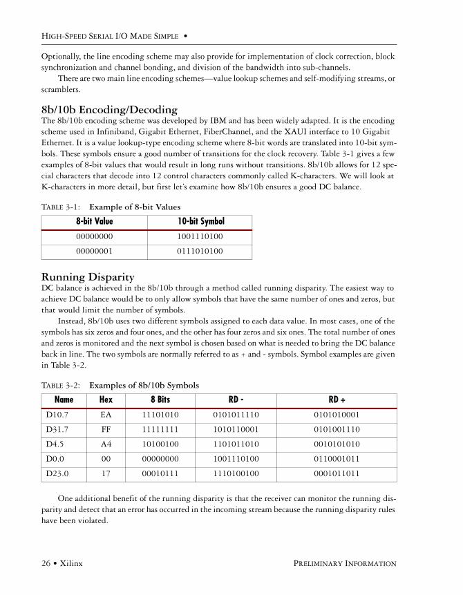
8b/10b Encoding/DecodingThe 8b/10b encoding scheme was developed by IBM and has been widely adapted. It is the encoding scheme used in Infiniband, Gigabit Ethernet, FiberChannel, and the XAUI interface to 10 Gigabit Ethernet. It is a value lookup-type encoding scheme where 8-bit words are translated into 10-bit sym-bols. These symbols ensure a good number of transitions for the clock recovery. Table 3-1 gives a few examples of 8-bit values that would result in long runs without transitions. 8b/10b allows for 12 spe-cial characters that decode into 12 control characters commonly called K-characters. We will look at K-characters in more detail, but first let’s examine how 8b/10b ensures a good DC balance.
Running DisparityDC balance is achieved in the 8b/10b through a method called running disparity. The easiest way to achieve DC balance would be to only allow symbols that have the same number of ones and zeros, but that would limit the number of symbols.
Instead, 8b/10b uses two different symbols assigned to each data value. In most cases, one of the symbols has six zeros and four ones, and the other has four zeros and six ones. The total number of ones and zeros is monitored and the next symbol is chosen based on what is needed to bring the DC balance back in line. The two symbols are normally referred to as + and - symbols. Symbol examples are given in Table 3-2.
One additional benefit of the running disparity is that the receiver can monitor the running dis-parity and detect that an error has occurred in the incoming stream because the running disparity rules have been violated.
TABLE 3-1: Example of 8-bit Values
8-bit Value 10-bit Symbol
00000000 1001110100
00000001 0111010100
TABLE 3-2: Examples of 8b/10b Symbols
Name Hex 8 Bits RD - RD +
D10.7 EA 11101010 0101011110 0101010001
D31.7 FF 11111111 1010110001 0101001110
D4.5 A4 10100100 1101011010 0010101010
D0.0 00 00000000 1001110100 0110001011
D23.0 17 00010111 1110100100 0001011011
TECHNOLOGY
PRELIMINARY INFORMATION XILINX • 27
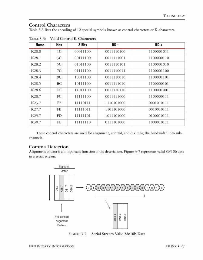
Control CharactersTable 3-3 lists the encoding of 12 special symbols known as control characters or K-characters.
These control characters are used for alignment, control, and dividing the bandwidth into sub-channels.
Comma DetectionAlignment of data is an important function of the deserializer. Figure 3-7 represents valid 8b/10b data in a serial stream.
TABLE 3-3: Valid Control K-Characters
Name Hex 8 Bits RD - RD +
K28.0 1C 00011100 0011110100 1100001011
K28.1 3C 00111100 0011111001 1100000110
K28.2 5C 01011100 0011110101 1100001010
K28.3 7C 01111100 0011110011 1100001100
K28.4 9C 10011100 0011110010 1100001101
K28.5 BC 10111100 0011111010 1100000101
K28.6 DC 11011100 0011110110 1100001001
K28.7 FC 11111100 0011111000 1100000111
K23.7 F7 11110111 1110101000 0001010111
K27.7 FB 11111011 1101101000 0010010111
K29.7 FD 11111101 1011101000 0100010111
K30.7 FE 11111110 0111101000 1000010111
FIGURE 3-7: Serial Stream Valid 8b/10b Data
0 0 1 1 1 1 1 0 0 01
Transmit
Order
Pre-defined
Alignment
Pattern
D1.
7
K28
.7
D31
.7
D30
.2 0 1 0 1 0
K28
.7
D31
.7
D30
.2

HIGH-SPEED SERIAL I/O MADE SIMPLE •
28 • Xilinx PRELIMINARY INFORMATION
How do we know where the symbol boundaries are? Symbols are delineated by a comma. Here, a comma is one or two symbols specified to be the comma or alignment sequence. This sequence is usu-ally settable in the transceiver, but in some cases it may be predefined.
The receiver scans the incoming data stream for the specified bit sequence. If it finds the sequence, the deserializer resets the word boundaries to match the detected comma sequence. This is a continuous scan. Once the alignment has been made, all subsequent commas detected should find the alignment already set. Of course, the comma sequence must be unique within any combination of sequences.
For example, if we are using a signal symbol c for the comma, then we must be certain that no ordered set of symbols xy contains the bit sequence c. Using a predefined protocol is not a problem since the comma characters have already been defined.
One or more of a special subset of K-characters is often used. The subset consists of K28.1, K28.5, and K28.7, all of which have 1100000 as the first seven bits. This pattern is only found in these char-acters; no ordered set of data and no other K-characters will ever contain this sequence. Hence, it is ideal for alignment use. In cases where a custom protocol is built, the safest and most common solu-tion is to “borrow” a sequence from a well-known protocol. Gigabit Ethernet uses K28.5 as its comma. Because of this it is often referred to as the comma symbol even though there are technically other choices.
The names used—such as D0.3 andK28.5— are derived from the way the encoders and decoders can be built. Figure 3-8 represents this method.
The 8-input bits are broken into 5- and 3-bit buses; that is how the names were developed. For example, the name Dx.y describes the data symbol for the input byte where the five least significant bits have a decimal value of x and the three most significant bits have a decimal value of y.
Comma: One or two symbols specified to be the alignment sequence.
FIGURE 3-8: Encoders/Decoders Block Diagram
5B/6BEncoder2
5-bit sub-block (LSB)
H G F E D C B A Z
1
3
0
6
5
7
4
a b c d e i f g h j
5
6
4
7
1
2
0
3
9
8
3B/4BEncoder3-bit sub-block (MSB)
8-bit ASCIIData Input
Control
RunningDisparity
6-bit encoded sub-block
4-bit encoded sub-block

TECHNOLOGY
PRELIMINARY INFORMATION XILINX • 29
A K indicates the control character. The three bits turn into four bits and the five bits turn into six. Another naming convention refers to the 8-bit bits as HGF EDCBA and 10-bit bits as abcdei fghj.
Overhead is one of the drawbacks to the 8b/10b scheme. To get 2.5 gigabits of bandwidth requires a wire speed of 3.125 Gb/s. Scrambling techniques can easily handle the clock transition and DC bias problems without a need for increased bandwidth.
ScramblingScrambling is a way of reordering or encoding the data so that it appears to be random, but it can still be unscrambled. We want randomizers that break up long runs of zeros and ones. Obviously, we want the descrambler to unscramble the bits without requiring any special alignment information. This characteristic is called a self-synchronizing code.
A simple scrambler consists of a series of flip-flops arranged to shift the data stream. Most of the flip-flops simply feed the next bit, but occasionally a flip-flop will be exclusively ORed or ANDed with an older bit in the stream. Figure 3-9 shows this concept.
The scrambling method is usually referred to as a polynomial because of the mathematics involved. Polynomials are chosen based on scrambling properties such as how random a stream they create, and how well they break up long runs of zeros and ones. They must also avoid generating long run lengths.
Scrambling: A way of reordering or encoding the data so that it appears random, but can be unscrambled.
FIGURE 3-9: Basic Scrambling Circuit
Data
Input
Data
OutputScrambled Data
Scrambler Descrambler
D0 Q D0 Q D0 QQ 0DQ 0DQ 0D
HIGH-SPEED SERIAL I/O MADE SIMPLE •
30 • Xilinx PRELIMINARY INFORMATION
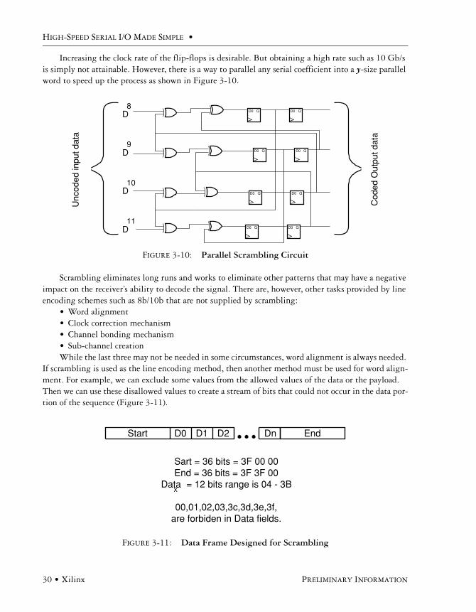
Increasing the clock rate of the flip-flops is desirable. But obtaining a high rate such as 10 Gb/s is simply not attainable. However, there is a way to parallel any serial coefficient into a y-size parallel word to speed up the process as shown in Figure 3-10.
Scrambling eliminates long runs and works to eliminate other patterns that may have a negative impact on the receiver’s ability to decode the signal. There are, however, other tasks provided by line encoding schemes such as 8b/10b that are not supplied by scrambling:
• Word alignment• Clock correction mechanism• Channel bonding mechanism• Sub-channel creationWhile the last three may not be needed in some circumstances, word alignment is always needed.
If scrambling is used as the line encoding method, then another method must be used for word align-ment. For example, we can exclude some values from the allowed values of the data or the payload. Then we can use these disallowed values to create a stream of bits that could not occur in the data por-tion of the sequence (Figure 3-11).
FIGURE 3-10: Parallel Scrambling Circuit
FIGURE 3-11: Data Frame Designed for Scrambling
D0 QD8
D10
D11
D9
D0 Q
D0 Q
D0 Q
D0 Q
D0 Q
D0 Q
D0 Q
Unc
oded
inpu
t dat
a
Cod
ed O
utpu
t dat
a
Start D0 D1 D2 EndDn
Sart = 36 bits = 3F 00 00End = 36 bits = 3F 3F 00
Data = 12 bits range is 04 - 3B
00,01,02,03,3c,3d,3e,3f,are forbiden in Data fields.
X
TECHNOLOGY
PRELIMINARY INFORMATION XILINX • 31
Normally, this would involve designing long run lengths that cannot occur in the data stream because of the disallowed values. The long runs will be broken by the scrambling and then restored when the stream is unscrambled. Downstream unscrambler logic looks for these patterns and aligns the data. Similar techniques can be used to install any of the other characteristics.
4b/5b 64b/66b4b/5b is similar to 8b/10b, but simpler. As the name implies, four bits are encoded into five bits with this scheme. 4b/5b offers simpler encoders and decoders than 8b/10b. But there are few control char-acters and it does not handle the DC balance or disparity problem. With the same coding overhead and less functionality, 4b/5b is not often used anymore. Its main advantage was implementation size, but gates are so cheap now that it is not much of an advantage. 4b/5b is still used in various standards including low bit rate versions of FiberChannel and Audio Engineering Society-10 (AES-10) or Mul-tichannel Audio Digital Interface (MADI), a digital audio multiplexing standard.
One of the new encoding methods is known as 64b/66b. We might think hat it is simply a ver-sion of 8b/10b that has less coding overhead, but the details are vastly different.
64b/66b came about as a result of user needs not being met by current technology. The 10 Giga-bit Ethernet community had a need for Ethernet-based communication at 10 Gb/s. And while they could use four links at a 2.5 Gb payload and 3.125-Gb/s wire speed, XERDES was approaching the ultimate 10 Gb solution in a single link. There were new SERDES that could run at just over 10 Gb/s, but could not be pushed to the 12.5 Gb needed to support 8b/10b overhead.
The laser driving diode was another issue. The telecommunications standard Synchronous Opti-cal Network (SONET) used lasers capable of just over 10 Gb. Faster lasers were much more expensive. The Gigabit Ethernet community could either give up or create something with a significantly lower overhead to replace 8b/10b. They chose 64b/66b.
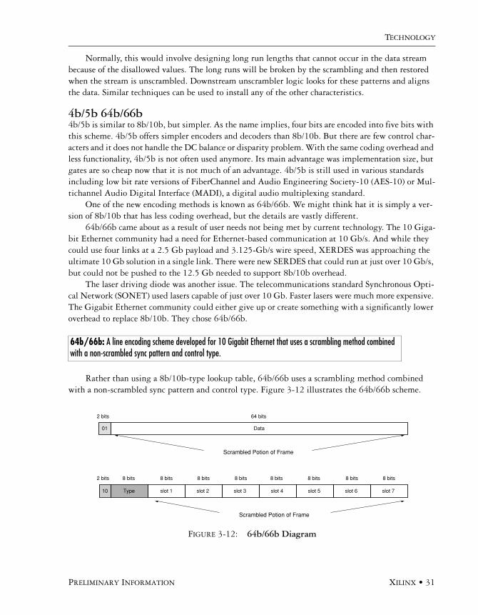
Rather than using a 8b/10b-type lookup table, 64b/66b uses a scrambling method combined with a non-scrambled sync pattern and control type. Figure 3-12 illustrates the 64b/66b scheme.
64b/66b: A line encoding scheme developed for 10 Gigabit Ethernet that uses a scrambling method combined with a non-scrambled sync pattern and control type.
FIGURE 3-12: 64b/66b Diagram
01 Data
2 bits 64 bits
Scrambled Potion of Frame
10 Type slot 1 slot 2 slot 3 slot 4 slot 5 slot 6 slot 7
Scrambled Potion of Frame
2 bits 8 bits 8 bits 8 bits 8 bits 8 bits 8 bits 8 bits 8 bits

HIGH-SPEED SERIAL I/O MADE SIMPLE •
32 • Xilinx PRELIMINARY INFORMATION
There are two main frame types. The simple main frame consists of a 2-bit sync pattern of 01 fol-lowed by 64 bits of data. The data is scrambled but the sync bits are not. The other frame type allows for control information as well as data. Control frames start with the 2-bit pattern 10. The eight bits in the type field define the format of the 56-bit payload. For example, if the type is hex 0xcc, then the pattern contains four bytes of data and three bytes of control (Figure 3-13).
There is also a zero-bit wide symbol associated with this frame (Figure 3-14).
How is a zero-bit wide symbol created? It is not actually 0 bits; it is part of the type byte that is projected into the payload. There are eight bits for the type field that would allow for 256 different types of payloads. Most 64b/66b systems define about 15 different types. And those 15 types simply define x data bytes followed by y control bit. They may also include a reversal x control then y data bytes. It is common to define the placement of these inferred symbols with some types. Common zero-
FIGURE 3-13: 0xcc Type Example
FIGURE 3-14: 0xcc Type with Symbol Shown
10 0xCC data data data data control control control
8 bits 8 bits 8 bits 8 bits 8 bits 8 bits 8 bits 8 bits
10 0xCC data data data data control control control
8 bits 8 bits 8 bits 8 bits 8 bits 8 bits 8 bits 8 bits
end
0 bits
TECHNOLOGY
PRELIMINARY INFORMATION XILINX • 33
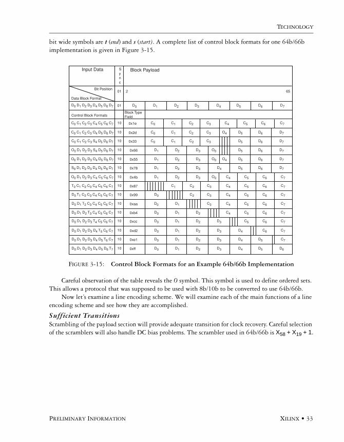
bit wide symbols are t (end) and s (start). A complete list of control block formats for one 64b/66b implementation is given in Figure 3-15.
Careful observation of the table reveals the O symbol. This symbol is used to define ordered sets. This allows a protocol that was supposed to be used with 8b/10b to be converted to use 64b/66b.
Now let’s examine a line encoding scheme. We will examine each of the main functions of a line encoding scheme and see how they are accomplished.
Sufficient TransitionsScrambling of the payload section will provide adequate transition for clock recovery. Careful selection of the scramblers will also handle DC bias problems. The scrambler used in 64b/66b is X58 + X19 + 1.
FIGURE 3-15: Control Block Formats for an Example 64b/66b Implementation
D0 D1 D2 D3 D4 D5 D6 T7 10
10D0 D1 D2 D3 D4 D5 T6 C7
10D0 D1 D2 D3 D4 T5 C6 C7
10D0 D1 D2 D3 T4 C5 C6 C7
10D0 D1 D2 T3 C4 C5 C6 C7
10D0 D1 T2 C3 C4 C5 C6 C7
10D0 T1 C2 C3 C4 C5 C6 C7
10T0 C1 C2 C3 C4 C5 C6 C7
10O0 D1 D2 D3 C4 C5 C6 C7
10O0 D1 D2 D3 O4 D5 D6 D7
10O0 D1 D2 D3 S4 D5 D6 D7
10C0 C1 C2 C3 S4 D5 D6 D7
10C0 C1 C2 C3 O4 D5 D6 D7
10C0 C1 C2 C3 C4 C5 C6 C7
01D0 D1 D2 D3 D4 D5 D6 D7
10S0 D1 D2 D3 D4 D5 D6 D7
Control Block FormatsBlock TypeField
Data Block Format
Bit Position
0x1e
0x2d
0x33
0x66
0x55
0x78
0x4b
0x87
0x99
0xaa
0xb4
0xcc
0xd2
D0
D0
Input Data Sync
Block Payload
01 2 65
D0 D1 D2 D3 D4 D5 D6 D7
D1
D1
D1
D1 D2
D2
C1 C2
C2
C4 C5
C5
C5
C5 C6
C6
C6
C6 C7
C7
C7
C7
C3
C2 C3 C4 C5 C6 C7C1C0
C1C0
C3 C4
C4
C4
O0
O0 O4
O4
C3
D0 C5 C6 C7C4C3C2
0xff D0 D1 D2 D3 D4 D5 D6
0xe1 D0 D1 C7D3 D4 D5D2
D0 D1 C6 C7D3 D4D2
D5 D6
D6 D7
D7
C3C1C0 C2 D6 D7D5
D5
D0 D1 C5 C6 C7D3D2
D2
D3
D1 D2 D6 D7D5D4D3
D3
D1 D2 O0 D6 D7D5D3

HIGH-SPEED SERIAL I/O MADE SIMPLE •
34 • Xilinx PRELIMINARY INFORMATION
Alignment64b/66b differs from other methods in the alignment procedure. Figure 3-16 shows how it works.
There will be a sync value of 01 or 10 every 66 bits. Those same bit combinations will appear in many other places as well. The alignment procedure selects a random starting point. It first looks for a valid sync (01 or 10 combination). If there isn’t one, it slips a bit and rechecks. Once a 01 or 10 com-bination is found, the position 66 bits later is checked. If that is a valid sync also, the process incre-ments the counter and checks the location 66 bits later. If enough sync markers are found in a row without any misses, the alignment is considered found. Any misses during the sequence forces the counter back to zero.
Once the alignment has been locked, missed syncs are considered errors. If enough errors occur in a period of time, the alignment is re-evaluated. At first glance, it appears that this algorithm would obtain lock within the maximum number of valid sync tries (+66 or less). But the high likelihood of the 01 and 10 sequences showing up in the data window can mean many false paths are taken for a long time before they are abandoned.
To speed lock time, some optional or alternative protocols have been suggested. They involve the replacement of data with special training or locking sequences that can ease alignment.
Clock CorrectionClock correction can be handled on byte or multi-byte boundaries, or on a 66-bit code word. A special type could be defined to be the clock correction symbol. The entire payload of the code word would not contain useful information and could be deleted or repeated as necessary. Alternatively, a byte-wide clock correction symbol could be defined as any unused value. Of course, if the SERDES we are using only supports one of these methods, we will need to use that particular method. The byte-wide method is the most common since it allows for smaller receive FIFO buffers and matches up better with legacy protocols.
Channel alignmentChannel alignment can be handled much like clock alignment, either as a special type or a sequence found within the control data.
Sub-ChannelsSub-channels can be handled like clock alignment, either as a special type or a sequence found within the control data.
4b/5b 64b/66b Trade-OffsThese functions comprise the overhead coding method that allowed 10 Gigabit Ethernet to use exist-ing SONET class laser diodes. Laser diodes are not the only similarity that this method has in common with SONET; SONET uses many of the same principles for alignment but is even more complicated than 64b/66b.
FIGURE 3-16: 64b/66b Alignment Procedure
66 bits 66 bits 66 bits 66 bits 66 bits 66 bits

TECHNOLOGY
PRELIMINARY INFORMATION XILINX • 35
The price for the lower overhead is longer alignment times, the possibility of a slight DC bias, and more complicated encoders and decoders. Complications such as turning the scramblers on and off for payload vs. sync and type fields make 64b/66b circuits more complicated than their 8b/10b cous-ins. There is also a complexity cost for using and setting up the encoder.
Introduction to PacketsSome designers feel that sending data over packets for anything but a local area network (LAN) is a complete waste. Let’s address that issue by first defining a packet.
Notice that there is nothing in the definition about source and destination addresses, CRCs, min-imum lengths, or Open Systems Interconnection (OSI) protocol layers. A packet is simply a data struc-ture with defined starting and ending points. While LAN packets often have many of these characteristics, there are many other uses of packets that are much simpler.
Packets are used everywhere to transfer information—automobile wiring harnesses, cell phones, and home entertainment centers, to name a few. But what do packets have to do with gigabit serial links?
Most data transferred across a gigabit serial link is embedded in some sort of packet. It's only nat-ural that a SERDES requires a method for aligning the incoming stream into words. This special bit sequence or comma must be sent if the system requires clock correction. The comma could be a natural marker for the beginning or end of a frame. If clock correction is required, the clock correction sequence is usually the ideal character. After adding a couple of ordered sets to indicate the end or start of the packet, and an ordered set to indicate a special type of packet, we have a simple, powerful trans-mission path.
The idle symbol, or sequence, is another important packet concept. This symbol is sent whenever there is no information to send. Continuous transmission of data ensures that the link stays aligned
Packet: A well-defined collection of bytes consisting of a header, data, and trailer.

HIGH-SPEED SERIAL I/O MADE SIMPLE •
36 • Xilinx PRELIMINARY INFORMATION
and that the PLL keeps the recovered clock locked. Figure 3-17 illustrates some sample packet formats from various standards.
Reference Clocking RequirementsThe input, or reference clock, of a Multi-Gigabit Transceiver (MGT) has very tight specifications. It includes a tight frequency requirement usually specified in allowable parts per million (PPM) of fre-quency error. It will also have strict jitter requirements defined in terms of time units (picoseconds) or unit intervals (UI).
Such tight requirements enable the PLL and clock extraction circuits to work. This often requires an accurate crystal oscillator on each printed circuit board (PCB) in the system that uses MGTs. These crystal oscillators are a step above most used for digital systems and will cost more. In many cases,
FIGURE 3-17: Packet Format Diagrams
PPM: Parts per million; a way of describing a very small ratio.
UI: Unit intervals; same as length of time as a symbol, i.e., 0.2 UI = 20% of the symbol time.
Jitter: Variation of the ideal transition placement.
10101010 ...
10101010
10101011
Preamble SFD
8 6 6 2 446-1500Preamble/
SDFDA SA Type Data FCS
8 6 6 2 446-1500Preamble/
SDFDA SA Length Data FCS
Preamble: 7 identical bytes; used fro synchronizationSFD (Start Frame Deliminator): Indicated the froam is about to beginDA (Destination Address): Contains the address of the frame's destinationSA (Source Address): Contains the address of the frame's senderLength: Indicates the number of data bytes (IEEE 802.3-based variants)Type: Indicates the upper-level protocol that is using the packet (Ethernet 1.0/2.0 Variants)Data: Contains the information being transmitted, which may consist of a higher-layer packet(may be padded)FCS: A frame check sequence
LSB
PreambleLSB
MSB
V U C B
0 3 4 7 8 27 28 31
Validity flag
Parity bit
User Data
Channel status
SF Data EF
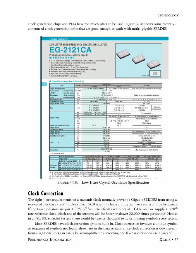
TECHNOLOGY
PRELIMINARY INFORMATION XILINX • 37
clock generation chips and PLLs have too much jitter to be used. Figure 3-18 shows some recently-announced clock generation units that are good enough to work with multi-gigabit SERDES.
Clock CorrectionThe tight jitter requirements on a transmit clock normally prevent a Gigabit SERDES from using a recovered clock as a transmit clock. Each PCB assembly has a unique oscillator and a unique frequency. If the two oscillators are just 1 PPM off frequency from each other at 1 GHz, and we supply a 1/20th rate reference clock, clock one of the streams will be faster or slower 20,000 times per second. Hence, in an 8b/10b encoded system there would be twenty thousand extra or missing symbols every second.
Most SERDES have clock correction options built in. Clock correction involves a unique symbol or sequence of symbols not found elsewhere in the data stream. Since clock correction is downstream from alignment, this can easily be accomplished by reserving one K-character or ordered pairs of
FIGURE 3-18: Low Jitter Crystal Oscillator Specification
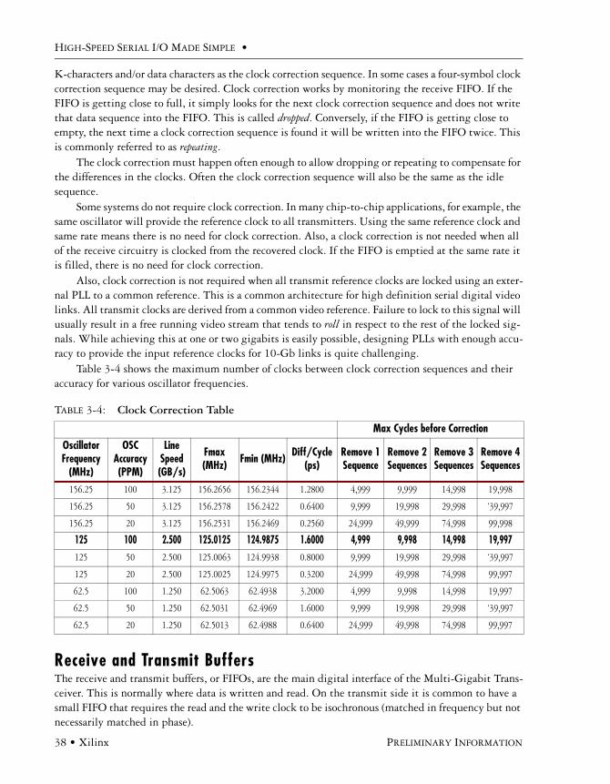
HIGH-SPEED SERIAL I/O MADE SIMPLE •
38 • Xilinx PRELIMINARY INFORMATION
K-characters and/or data characters as the clock correction sequence. In some cases a four-symbol clock correction sequence may be desired. Clock correction works by monitoring the receive FIFO. If the FIFO is getting close to full, it simply looks for the next clock correction sequence and does not write that data sequence into the FIFO. This is called dropped. Conversely, if the FIFO is getting close to empty, the next time a clock correction sequence is found it will be written into the FIFO twice. This is commonly referred to as repeating.
The clock correction must happen often enough to allow dropping or repeating to compensate for the differences in the clocks. Often the clock correction sequence will also be the same as the idle sequence.
Some systems do not require clock correction. In many chip-to-chip applications, for example, the same oscillator will provide the reference clock to all transmitters. Using the same reference clock and same rate means there is no need for clock correction. Also, a clock correction is not needed when all of the receive circuitry is clocked from the recovered clock. If the FIFO is emptied at the same rate it is filled, there is no need for clock correction.
Also, clock correction is not required when all transmit reference clocks are locked using an exter-nal PLL to a common reference. This is a common architecture for high definition serial digital video links. All transmit clocks are derived from a common video reference. Failure to lock to this signal will usually result in a free running video stream that tends to roll in respect to the rest of the locked sig-nals. While achieving this at one or two gigabits is easily possible, designing PLLs with enough accu-racy to provide the input reference clocks for 10-Gb links is quite challenging.
Table 3-4 shows the maximum number of clocks between clock correction sequences and their accuracy for various oscillator frequencies.
Receive and Transmit BuffersThe receive and transmit buffers, or FIFOs, are the main digital interface of the Multi-Gigabit Trans-ceiver. This is normally where data is written and read. On the transmit side it is common to have a small FIFO that requires the read and the write clock to be isochronous (matched in frequency but not necessarily matched in phase).
TABLE 3-4: Clock Correction Table
Max Cycles before CorrectionOscillator Frequency
(MHz)
OSC Accuracy (PPM)
Line Speed (GB/s)
Fmax (MHz) Fmin (MHz) Diff/Cycle
(ps)Remove 1 Sequence
Remove 2 Sequences
Remove 3 Sequences
Remove 4 Sequences
156.25 100 3.125 156.2656 156.2344 1.2800 4,999 9,999 14,998 19,998
156.25 50 3.125 156.2578 156.2422 0.6400 9,999 19,998 29,998 ‘39,997
156.25 20 3.125 156.2531 156.2469 0.2560 24,999 49,999 74,998 99,998
125 100 2.500 125.0125 124.9875 1.6000 4,999 9,998 14,998 19,997125 50 2.500 125.0063 124.9938 0.8000 9,999 19,998 29,998 ‘39,997
125 20 2.500 125.0025 124.9975 0.3200 24,999 49,998 74,998 99,997
62.5 100 1.250 62.5063 62.4938 3.2000 4,999 9,998 14,998 19,997
62.5 50 1.250 62.5031 62.4969 1.6000 9,999 19,998 29,998 ‘39,997
62.5 20 1.250 62.5013 62.4988 0.6400 24,999 49,998 74,998 99,997

TECHNOLOGY
PRELIMINARY INFORMATION XILINX • 39
A different scheme is used in cases where the tx_write and tx_read strobes are not of the exact same frequency. Here, a larger FIFO is used and its current status is constantly monitored. If the FIFO is filling it will eventually overrun. In this case the incoming stream is monitored for idle symbols. When encountered they are not written into the FIFO.
Conversely, if the FIFO is running low when an idle is found on the output, the data is brought to the user. The write pointer is not moved causing the idle to be repeated. It is important for idle sym-bols to be used instead of byte alignment, comma symbols, clock correction sequences, or channel bonding sequences. All these are needed downstream at some guaranteed delivery rate.
The receive FIFO built into an MGT is usually considerably deeper than the transmit (Tx) buffer. Its main purpose is to allow for clock correction and channel bonding.
Channel BondingSometimes there is a need to move more data than can fit on one serial link. In these cases multiple links are used in parallel to transmit the data. When this is done, incoming streams must be aligned. This process is commonly referred to as channel bonding. Channel bonding absorbs the skew between two or more MGTs and presents the data to the user as if it were transmitted over a single link (Figure 3-19).
Isochronous: Matched in frequency but not necessarily matched in phase.
FIGURE 3-19: Channel Bonding Block Diagram
P Q R S T
P Q R S T
P Q R S T
P Q R S T
Full word SSSS sent over four channels, one byte per channel
In Transmitters:
Channel (lane) 0
Channel (lane) 1
Channel (lane) 2
Channel (lane) 3
P Q R S T
P Q R S T
P Q R S T
P Q R S T
P Q R S T
P Q R S T
P Q R S T P Q R S T
In Receivers:Read
RXUSRCLK
Read
RXUSRCLK
Before channel bonding After channel bonding
HIGH-SPEED SERIAL I/O MADE SIMPLE •
40 • Xilinx PRELIMINARY INFORMATION
There are several causes of data skew between multiple MGTs:• Differences in transmission path length• Active repeaters in transmission path• Differences because of clock correction• Differences in time to lock/byte alignmentSince channel bonding requires communication between transceivers, the exact details will vary
from vendor to vendor and part to part. Some common traits are designation of one channel as the mas-ter channel, designation of slaves, and possibly the designation of forwarding slaves. Three-level chan-nel bonding that includes a master and forwarding slaves is sometimes referred to as two-hop channel bonding.
The channel bonding sequence must be unique and expandable and it must be ignored down-stream because it may be added or dropped. There are normally a minimum number of symbols between a clock correction sequence and a channel bonding sequence. Many 8b/10b-based standard protocols specify a minimum of four symbols between clock correction and channel bonding sequences. Hence, four symbols or bytes is a common separation distance.
Physical SignalingThe physical implementation of multi-gigabit SERDES universally takes the form of differential-based electrical interfaces. There are three common differential signal methods—Low-Voltage Differ-ential Signaling (LVDS), Low Voltage Pseudo Emitter-Coupled Logic (LVPECL), and Current Mode Logic (CML). CML is preferred for the gigabit link. It has the most common interface type and often provides for either AC or DC termination and selectable output drive. Some inputs provide built-in line equalization and/or internal termination. Often the termination impedance is selectable as well.
Channel Bonding: Absorbs the skew between two or more MGTs and presents the data to the user as if it were transmitted over a single link.
Front-end and back-end together make up the physical interface.
CML: Current Mode Logic; a differential-based electrical interface well suited to the gigabit link.
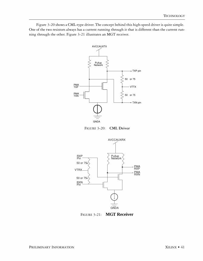
TECHNOLOGY
PRELIMINARY INFORMATION XILINX • 41
Figure 3-20 shows a CML-type driver. The concept behind this high-speed driver is quite simple. One of the two resistors always has a current running through it that is different than the current run-ning through the other. Figure 3-21 illustrates an MGT receiver.
FIGURE 3-20: CML Driver
FIGURE 3-21: MGT Receiver
PMATXP
PMATXN
AVCCAUXTX
50 or 75
50 or 75
TXP pin
TXN pin
VTTX
PullupNetwork
GNDA
RXPPin
RXNPin
AVCCAUXRX
50 or 75
50 or 75
VTRX
PullupNetwork
GNDA
PMARXPPMARXN

HIGH-SPEED SERIAL I/O MADE SIMPLE •
42 • Xilinx PRELIMINARY INFORMATION
Figures 3-22 and Figure 3-23 list data sheets for the analog front-end and back-end.
Pre-EmphasisPerhaps the most important characteristic of a multi-gigabit driver is its ability to perform pre-emphasis. Pre-emphasis is the intentional overdriving at the beginning of a transition. To the inexpe-rienced eye it looks like a fault; it looks like overshoot and undershoot that can indicate a bad design. To understand why this is done, we need to understand inter-symbol interference (ISI).
FIGURE 3-22: Differential Receiver Parameters
FIGURE 3-23: Differential Transmitter Parameters
Pre-emphasis: Intentional overdriving at the first of a transition.

TECHNOLOGY
PRELIMINARY INFORMATION XILINX • 43
ISI occurs when the serial stream contains a number of bit times of the same value followed by short (1 or 2) bit times of the opposite value. The medium (transmission path capacitance) has less time to charge during the shorter value time, so it produces lower amplitude.
With ISI, the larger runs allow for maximum charge but the single bit time cannot compensate. It is at risk of not being detected. Figure 3-24, Figure 3-25, and Figure 3-26 show this phenomena. The solution to this problem is to overdrive the first of each transition, or underdrive any consecutive bit times of the same value. This is sometimes called de-emphasis.
ISI: Inter-symbol interference—Occurs when the serial stream contains a number of bit times of the same value followed by short bit times of the opposite value.
FIGURE 3-24: Inter-Symbol Interference
LD V -
V +
time
effect ofISI
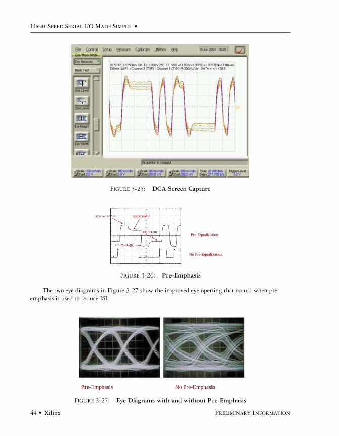
HIGH-SPEED SERIAL I/O MADE SIMPLE •
44 • Xilinx PRELIMINARY INFORMATION
The two eye diagrams in Figure 3-27 show the improved eye opening that occurs when pre-emphasis is used to reduce ISI.
FIGURE 3-25: DCA Screen Capture
FIGURE 3-26: Pre-Emphasis
FIGURE 3-27: Eye Diagrams with and without Pre-Emphasis
No Pre-Equalization
Pre-Equalization
STRONG HIGH LOGIC HIGH
STRONG LOW
LOGIC LOW
Pre-Emphasis No Pre-Emphasis

TECHNOLOGY
PRELIMINARY INFORMATION XILINX • 45
Pre-emphasis can be implemented by using two CML drivers in parallel where one is delayed one bit time after the other. Figures 3-28 and 3-29 show a sample circuit and the waveforms that drive the transistors to obtain the output.
Differential Transmission LinesDigital design engineers and PCB designers once thought of traces as simple interconnects or wires. In fact, prototypes were built using a technique called wire warping. Transmission lines and transmission line theory were not necessarily applied. When the propagation delay of the trace was a tiny fraction
Eye pattern: Common waveform viewed on digital sampling scopes. It is an indication of the quality of the signal. Jitter, impedance matching, and amplitude can all be characterized through eye patterns.
FIGURE 3-28: Pre-Emphasis CML Schematic
FIGURE 3-29: Timing Diagrams for CML Circuit in Figure 3-28

HIGH-SPEED SERIAL I/O MADE SIMPLE •
46 • Xilinx PRELIMINARY INFORMATION
of the rise time of the signal, this was satisfactory. But as signals increased in frequency, transmission line theory had to move into the PCB design process.
For multi-gigabit operation this includes not only transmission lines and controlled impedance, but differential pair controlled impedance as well.
Differential pair impedance matched traces are two traces that run adjacent to each other. The spacing between the pair allows for a coupling to occur between the traces. The coupling is called weak (Figure 3-30) if the traces are relatively far apart. If the traces are closer it is called strong (Figure 3-31).
FIGURE 3-30: Weakly Coupled
FIGURE 3-31: Strongly Coupled

TECHNOLOGY
PRELIMINARY INFORMATION XILINX • 47
The coupling also affects the impedance of the trace if a given trace length and layer stack will make a given impedance. The same geometry for a differential pair will have a different impedance. The exact dimensions for any given impedance varies on material, but the board manufacturer can often provide the exact dimensions.
A tool/mathematical model called a field solver can calculate the numbers as well. Figure 3-32 shows the main types of controlled impedance differential traces—microstrip, stripline, offset strip-line, and broadside coupled. Table 3-5 includes controlled impedance differential trace types.
Line EqualizationEqualization is an attempt to compensate for differences in impedance/losses relative to frequency. Equalizers come in many forms but can generally be divided into passive and active types.
A passive equalizer is a passive circuit that has a frequency response that is complementary to the transmission losses. A passive equalizer can be thought of as a filter. If we filter out the frequencies that
FIGURE 3-32: Controlled Impedance Differential Traces
TABLE 3-5: Types of Controlled Impedance Differential Traces
Type Pros Cons
Microstrip Less loss than internal traces Only two layers (top and bottom)
More susceptible to interference
Stripline Better shielding
More possible layers
More amplitude loss per inch in high frequency signals than microstrip
Offset Stripline Useful if non-symmetrical Stack-up is needed.
Can be used to limit the number of power/gnd planes.
If used to save layers, the offset area above the traces should be kept free of other traces and must be free of parallel traces.
Broadside-coupled Very tight coupling The broadside coupled is difficult to manufacture because of tight tolerances and it is not recommended for multi-gigabit operation.
Active equalizer: Frequency dependant amplifiers/attenuators.
Passive equalizer: A passive circuit with a frequency response that is complementary to the transmission losses; similar to a filter.

HIGH-SPEED SERIAL I/O MADE SIMPLE •
48 • Xilinx PRELIMINARY INFORMATION
the transmission line passes, and not filter those that it does not pass, we can flatten the overall response as shown in Figure 3-33.
The active equalizers can be thought of as frequency-dependant amplifiers/attenuators. There are two types of active equalizers—fixed pattern and self-adjusting. No matter what the incoming data stream looks like, the fixed pattern active equalizer has the same frequency response (Figure 3-34 and Figure 3-35).
FIGURE 3-33: Unequalized System Frequency Response Example
FIGURE 3-34: Equalizer Frequency Response Example
Path
Path
EQ
EQ

TECHNOLOGY
PRELIMINARY INFORMATION XILINX • 49
This set gain attenuation pattern may be user-selectable or programmable. Some have a simple control—n settings with high or low gain. They are similar to the bass control on a simple audio sys-tem. Or they could allow for individual settings at various frequency bands much like the equalizer settings on a more complex audio system. A chart showing the possible frequency response for one such equalizer is shown in Figure 3-36.
The self-adjusting, or learning, equalizer is more complicated. It analyzes the incoming signal and detects which frequencies are being attenuated by the transmission path. Adjustments and mea-surements are made in a closed loop-type system. A self-adjusting equalizer is dependent on the incoming bit stream.
FIGURE 3-35: Equalized System Frequency Response Example
FIGURE 3-36: Sample Equalizer Frequency Response
Fixed pattern and self-adjusting are the two types of active equalizers.
Equalized Path
Equalized Path

HIGH-SPEED SERIAL I/O MADE SIMPLE •
50 • Xilinx PRELIMINARY INFORMATION
Often this type of equalizer is designed to work with a specific type of line encoding scheme. Learning equalizers are best suited for links with variable channels such as variable cable lengths or backplanes systems with significant differences in slot positions.
Fixed equalizers are better suited for systems with no variability such as chip-to-chip, balanced backplanes, and fixed-length cable systems. Equalizers are sometimes included in the analog front end of the SERDES or added to a system as a separate component (Figure 3-37).
Cables can also be equalized. The most common cable equalization technique is to add a passive equalizing circuit in the cable assembly, usually in the connector.
FIGURE 3-37: Sample Fact Sheet for an External 3G Equalizer
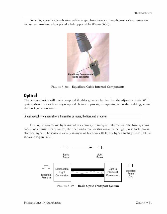
TECHNOLOGY
PRELIMINARY INFORMATION XILINX • 51
Some higher-end cables obtain equalized-type characteristics through novel cable construction techniques involving silver plated solid copper cables (Figure 3-38).
OpticalThe design solution will likely be optical if cables go much further than the adjacent chassis. With optical, there are a wide variety of optical choices to pass signals upstairs, across the building, around the block, or across town.
Fiber optic systems use light instead of electricity to transport information. The basic systems consist of a transmitter or source, the fiber, and a receiver that converts the light pulse back into an electrical signal. The source is usually an injection laser diode (ILD) or a light emitting diode (LED) as shown in Figure 3-39.
FIGURE 3-38: Equalized Cable Internal Components
A basic optical system consists of a transmitter or source, the fiber, and a receiver.
FIGURE 3-39: Basic Optic Transport System
Equalizing Componentsinside connector
Electrical toLight
Conversion
LightPulse
LightPulse
ElectricalPulse In
Light toElectrical
Conversion
ElectricalPulseOut
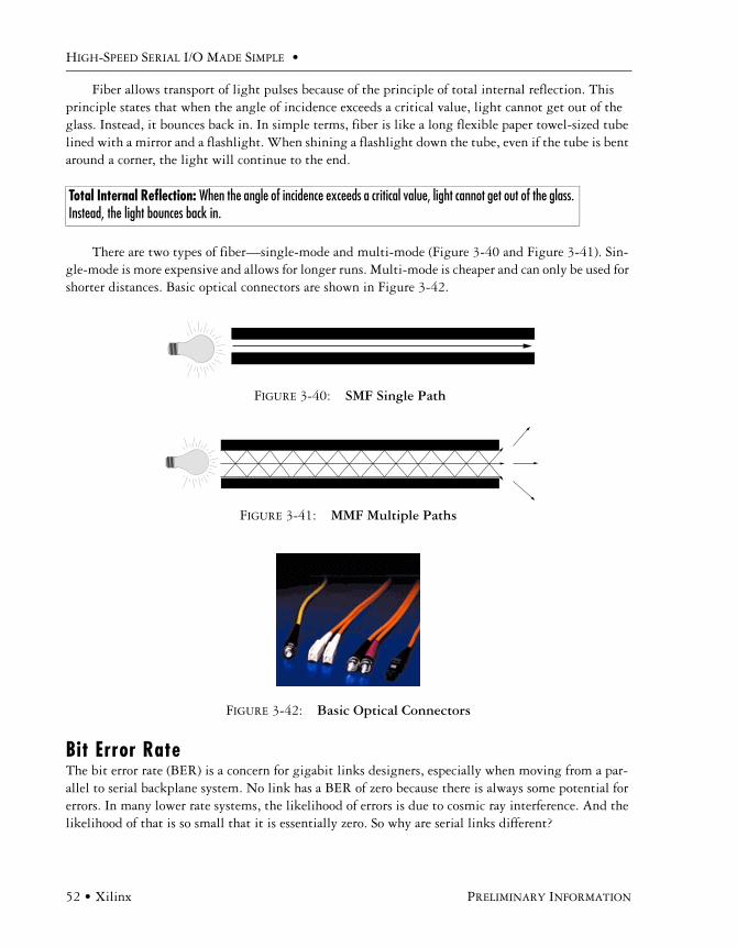
HIGH-SPEED SERIAL I/O MADE SIMPLE •
52 • Xilinx PRELIMINARY INFORMATION
Fiber allows transport of light pulses because of the principle of total internal reflection. This principle states that when the angle of incidence exceeds a critical value, light cannot get out of the glass. Instead, it bounces back in. In simple terms, fiber is like a long flexible paper towel-sized tube lined with a mirror and a flashlight. When shining a flashlight down the tube, even if the tube is bent around a corner, the light will continue to the end.
There are two types of fiber—single-mode and multi-mode (Figure 3-40 and Figure 3-41). Sin-gle-mode is more expensive and allows for longer runs. Multi-mode is cheaper and can only be used for shorter distances. Basic optical connectors are shown in Figure 3-42.
Bit Error Rate The bit error rate (BER) is a concern for gigabit links designers, especially when moving from a par-allel to serial backplane system. No link has a BER of zero because there is always some potential for errors. In many lower rate systems, the likelihood of errors is due to cosmic ray interference. And the likelihood of that is so small that it is essentially zero. So why are serial links different?
Total Internal Reflection: When the angle of incidence exceeds a critical value, light cannot get out of the glass. Instead, the light bounces back in.
FIGURE 3-40: SMF Single Path
FIGURE 3-41: MMF Multiple Paths
FIGURE 3-42: Basic Optical Connectors

TECHNOLOGY
PRELIMINARY INFORMATION XILINX • 53
There are three reasons: 1. Cosmic rays can cause errors especially if they happen to hit during a transition. The faster the
signal, the more transitions and the more likely a cosmic ray will occur during a transition.2. For any given BER, the faster the signal, the more likelihood of an error.3. High-speed clock data recovery is not an exact science. Jitter, ISI, and a host of other real world
interferences can cause a bad data decision that results in an error. For example, PLLs, areconstantly trying to adjust to the changing incoming signal. And as oscillators drift withtemperature, errors can occur.
Realities of TestingWhile the above reasons have a real effect, careful analysis of parallel backplanes, source synchronous links, or any communication channel could find similar faults. But for the most part, these are rou-tinely assumed to be close to zero and ignored.
Why shouldn't we have the same concerns in Gigabit SERDES? Because their original environ-ment is the communication industry with long and short haul optic transports. This is an industry that has always worried, tested, designed, and specified BERs. And this has had the most impact on Gigabit SERDES BER.
Some of the standards such as XAUI and some of the SONET variations specify a maximum BER. Unfortunately, testing for BER is difficult, boring, and time consuming. And it gets exponentially more difficult to get a unit of improvement. BERs are normally expressed in 10-x notation, so to move from 10-8 to a 10-9 takes 10-x the time. Testing becomes impractical at some point. Hence, most manufacturers test to the tightest BER in a published standard and no further.
CRCBut a designer must still design a system that is robust. To do so, he must first examine the system requirements to see if he can use the same commonly-used methods that contributed to the problem.
One method is error detection data retransmission. The incoming data is examined for errors. If any are discovered, a message is sent to the sender to retransmit. The preferred method for error detec-tion is CRC. This is so common that many SERDES include CRC generation and checking hardware directly within the SERDES. Often, the retransmission request is built into an upper level protocol. This is the best solution if the protocol used supports CRCs and retransmission, or if the data require-ments are such that they can be implemented.
If this is not possible, there are other options. The designer could simply build and test the system and see if it works. The published BER for the selected SERDES is a specification of how far it was tested, so the designer has some room to maneuver. It is possible that he can build a system far better than the published number. Besides being a specified testing stop point, the testing was probably done at the extremes (input jitter very near the maximum, etc.). If he designs the system to provide a better input stream, he will get better results.
Data offers another option to consider. Most data streams have a pattern and they are much more predictable than the pseudo-random bit streams used for BER testing. This can be good or bad depending on how the transmission path and equalizers react to the stream. This must be tested and adjusted.
So it is not completely far-fetched to build a system and see if it will work. However, if doing this presents a management concern, forward error correction (FEC) can alleviate concerns.
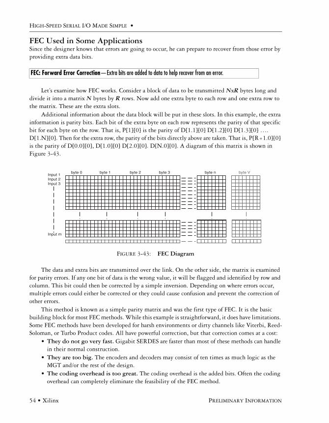
HIGH-SPEED SERIAL I/O MADE SIMPLE •
54 • Xilinx PRELIMINARY INFORMATION
FEC Used in Some ApplicationsSince the designer knows that errors are going to occur, he can prepare to recover from those error by providing extra data bits.
Let’s examine how FEC works. Consider a block of data to be transmitted NxR bytes long and divide it into a matrix N bytes by R rows. Now add one extra byte to each row and one extra row to the matrix. These are the extra slots.
Additional information about the data block will be put in these slots. In this example, the extra information is parity bits. Each bit of the extra byte on each row represents the parity of that specific bit for each byte on the row. That is, P[1][0] is the parity of D[1.1][0] D[1.2][0] D[1.3][0] …. D[1.N][0]. Then for the extra row, the parity of the bits directly above are taken. That is, P[R+1.0][0] is the parity of D[0.0][0], D[1.0][0] D[2.0][0]. D[N.0][0]. A diagram of this matrix is shown in Figure 3-43.
The data and extra bits are transmitted over the link. On the other side, the matrix is examined for parity errors. If any one bit of data is the wrong value, it will be flagged and identified by row and column. This bit could then be corrected by a simple inversion. Depending on where errors occur, multiple errors could either be corrected or they could cause confusion and prevent the correction of other errors.
This method is known as a simple parity matrix and was the first type of FEC. It is the basic building block for most FEC methods. While this example is straightforward, it does have limitations. Some FEC methods have been developed for harsh environments or dirty channels like Viterbi, Reed-Soloman, or Turbo Product codes. All have powerful correction, but that correction comes at a cost:
• They do not go very fast. Gigabit SERDES are faster than most of these methods can handle in their normal construction.
• They are too big. The encoders and decoders may consist of ten times as much logic as the MGT and/or the rest of the design.
• The coding overhead is too great. The coding overhead is the added bits. Often the coding overhead can completely eliminate the feasibility of the FEC method.
FEC: Forward Error Correction—Extra bits are added to data to help recover from an error.
FIGURE 3-43: FEC Diagram
Input 1Input 2Input 3
Input m
byte 0 byte 1 byte 2 byte 3 byte n byte V

TECHNOLOGY
PRELIMINARY INFORMATION XILINX • 55
SERDES Technology Facilitates I/O DesignI/O design is facilitated by tapping the functions available in SERDES technology. SERDES func-
tions such as RX align, clock manager, transmit/receive FIFO, and line encoder/decoder are used extensively to improve speed and accuracy. As SERDES plays a more important role in future I/O designs, its functions will continue to provide tools for more efficient I/O devices.

HIGH-SPEED SERIAL I/O MADE SIMPLE •
56 • Xilinx PRELIMINARY INFORMATION

PRELIMINARY INFORMATION XILINX • 57
CHAPTER 4
Designing with Gigabit Serial I/O
Understanding the challenges and trade-offs
The Challenges of Multi-Gigabit Transceiver DesignUnderstanding the individual challenges is the key to beginning to solve any engineering problem. When designing a Multi-Gigabit Transceiver (MGT), those challenges include understanding trans-ceiver protocols, signal integrity, impedance and power requirements, shielding requirements, printed circuit board (PCB) design requirements, and connector and cable selection requirements. Simulation and testing of the prototype are also critically important to a successful MGT design.
Design Considerations and Choices You Can UseThis chapter presents a broad view of the challenges and choices facing any MGT designer, and pre-sents the most common methods of dealing with those challenges when a SERDES is at the heart of the design. It describes various available transmission protocols, and the advantages and disadvantages of each. Signal and power considerations are discussed, as is the critical importance of shielding when designing fast links. Printed circuit board design requirements are explained, with connector and cable selection discussed. And, finally, the importance of, and approaches to, simulation of the MGT design (both analog and digital) are discussed. The chapter closes with an in-depth discussion of pro-totype test and measurement, some important debugging hints, and final suggestions.
ProtocolsSerializer/Deserializers (SERDESs) by themselves are relatively flexible devices. To set them up, you must define an alignment sequence, a clock correction sequence, the line encoding method, and the physical connection, and data will flow between the two transceivers. But the meaning of that data requires more definition, and that is the purpose of the protocols. What data is transmitted to where, what the data means, what is inserted in the data, what can be discarded, are defined by protocols.
Protocols for MGTs can vary greatly in scope, from simple data definitions to complex interfaces to upper level protocols. Items that can be specified in a multi-gigabit protocol include:

HIGH-SPEED SERIAL I/O MADE SIMPLE •
58 • Xilinx PRELIMINARY INFORMATION
• Data formats: Value definitions for video and audio protocols; how we use the ones and zeros to represent specific values or meanings.
• Sub-channels: Often there is a need for several different channels over the same link. Some of the common uses of sub-channels are control, status, and auxiliary data path.
• Data striping: A common function of a protocol is to define of how and where the data is separated from the overhead. This is commonly referred to as striping or de-embedding.
• Embedding: A protocol often defines how and where the data is embedded into the protocol streams or packets. This is especially true of protocols that follow the protocol stack model.
• Errors detection and handling: A protocol defines how errors are detected and what happens if there is an error.
• Flow control: Protocols may also define flow control. This can vary, from defining a way of dynamically scaling sub-channel bandwidth allocation to varying the idle insertion rate to match the clock correction needs.
• Addressing/switching/forwarding: While the direct point-to-point nature of a serial protocol eliminates many of the needs for an addressing scheme, some of the more complex protocols include addressing schemes. With addressing comes the possibility for forwarding and switching.
• Physical interface: Drive levels, pre-emphasis, and more, are specified by the protocol to ensure compatibility between devices.
Often the protocol choice is simple. When building a PCI Express card, simply run the PCI Express protocol. But when building a proprietary system, the system architect must decide whether to use a predefined protocol or design a custom protocol.
Standard ProtocolsThe next few pages provide a very brief look at some industry standard protocols (the full definitions of these standards may include many pages of text, and are not provided here):
XAUI: A 4-channel interface (2.5 Gb/s payload, 3.125 Gb/s wire speed) for 10-Gigabit Ethernet.PCI Express: Takes the old parallel PCI structure and updates it to a high-speed serial structure.
Upper levels of the protocol remain compatible, providing an easy adaptation into legacy PCI systems.Serial RapidIO: Another serial version of an older parallel spec, RapidIO is quite flexible and
sometimes used as a method of interfacing to multiple protocols such as PCI and Infiniband.FiberChannel: FiberChannel has always been a serial standard, but its speeds have increased over
the years. As copper interconnects have advanced, it has also become available on copper as well as fiber optics.
Infiniband: A box-to-box protocol run over either copper or fiber. Infiniband-style cables have become highly popular for multi-gigabit links of a few meters range. The specification allows for a variety of devices and complexity, and includes specifications for repeaters, and switches or hubs to

DESIGNING WITH GIGABIT SERIAL I/O
PRELIMINARY INFORMATION XILINX • 59
expand the number of connected devices. Infiniband can also be used for complex system configura-tions using Infiniband switches and control consoles (Figure 4-1).
Advanced Switching: A switched fabric protocol built on the same physical and data level pro-tocol as PCI Express. An emerging standard set to be significant in the switched fabric area.
FIGURE 4-1: Infiniband Switches and Control Consoles
CPU CPU CPU
Mem HCA
RAID Subsystem
SCSI
SCSI
SCSI
SCSI
SCSI
Processor
Mem
TCA
Consoles
Switch
Switch Switch
Switch Switch Switch
Switch
TC
A
IO M
odul
e
TC
A
IO M
odul
e
TC
A
IO M
odul
e
TC
A
IO M
odul
e
TC
A
IO M
odul
e
TC
A
IO M
odul
e
TC
A
IO M
odul
e
TC
A
IO M
odul
e
TC
A
IO M
odul
e
TC
A
IO M
odul
e
I/OChassis
I/OChassis
SCSI
Ethernet GraphicsVideo
Fibre Channelhub & FCdevices
Storage
Router
TCA
Controller
StorageSubsystem
Other IB SubnetsWANsLANsProcessor Nodes
Fabric(Subnet)
Processor Node
CPU CPU CPU
Mem HCAHCA
Processor Node
CPU CPU CPU
Mem HCAHCA
Processor Node
HCA = InfiniBand Channel Adapter in Processor nodeTCA = Infiniband Channel Adapter in I/O node

HIGH-SPEED SERIAL I/O MADE SIMPLE •
60 • Xilinx PRELIMINARY INFORMATION
PICMG: PICMG is a consortium of over 600 companies who collaboratively develop open spec-ifications for high-performance standardized backplane architectures. Many of these standards use other industry standards such as PCI and Infiniband.
ATCA: Also known as the Advanced Telecom Computing Architecture or AdvancedTCA, this PICMG standard is a specification for next generation telecommunication cabinets. Its aim is to ease multi-vendor inter operability while providing a very flexible, very scalable system. The standard has various implementations within a common theme. Included are architectures for star-based back-planes, redundant star-based backplanes, and fully connected mesh architectures.
FIGURE 4-2: Example ATCA Card
FIGURE 4-3: PICMG 3.0 Backplane
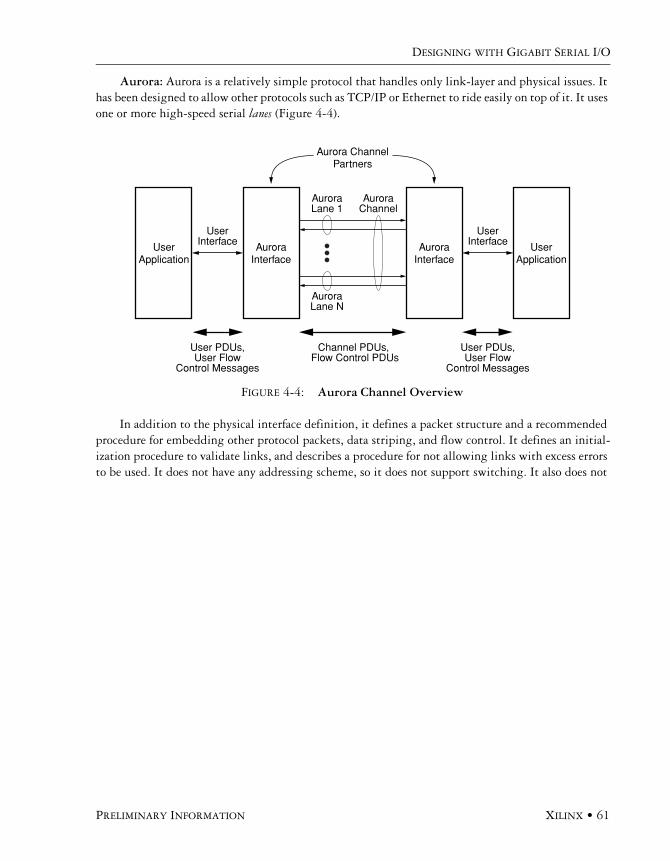
DESIGNING WITH GIGABIT SERIAL I/O
PRELIMINARY INFORMATION XILINX • 61
Aurora: Aurora is a relatively simple protocol that handles only link-layer and physical issues. It has been designed to allow other protocols such as TCP/IP or Ethernet to ride easily on top of it. It uses one or more high-speed serial lanes (Figure 4-4).
In addition to the physical interface definition, it defines a packet structure and a recommended procedure for embedding other protocol packets, data striping, and flow control. It defines an initial-ization procedure to validate links, and describes a procedure for not allowing links with excess errors to be used. It does not have any addressing scheme, so it does not support switching. It also does not
FIGURE 4-4: Aurora Channel Overview
AuroraLane 1
AuroraInterface
AuroraChannel
AuroraLane N
Aurora ChannelPartners
UserApplication
UserApplication
UserInterface
UserInterface
User PDUs,User Flow
Control Messages
User PDUs,User Flow
Control Messages
Channel PDUs, Flow Control PDUs
AuroraInterface
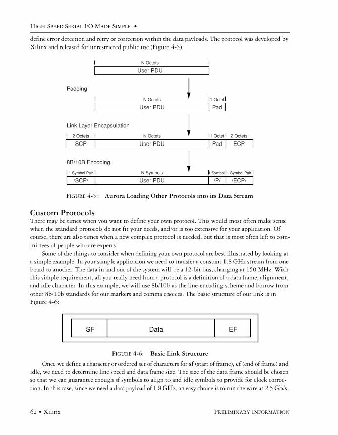
HIGH-SPEED SERIAL I/O MADE SIMPLE •
62 • Xilinx PRELIMINARY INFORMATION
define error detection and retry or correction within the data payloads. The protocol was developed by Xilinx and released for unrestricted public use (Figure 4-5).
Custom ProtocolsThere may be times when you want to define your own protocol. This would most often make sense when the standard protocols do not fit your needs, and/or is too extensive for your application. Of course, there are also times when a new complex protocol is needed, but that is most often left to com-mittees of people who are experts.
Some of the things to consider when defining your own protocol are best illustrated by looking at a simple example. In your sample application we need to transfer a constant 1.8 GHz stream from one board to another. The data in and out of the system will be a 12-bit bus, changing at 150 MHz. With this simple requirement, all you really need from a protocol is a definition of a data frame, alignment, and idle character. In this example, we will use 8b/10b as the line-encoding scheme and borrow from other 8b/10b standards for our markers and comma choices. The basic structure of our link is in Figure 4-6:
Once we define a character or ordered set of characters for sf (start of frame), ef (end of frame) and idle, we need to determine line speed and data frame size. The size of the data frame should be chosen so that we can guarantee enough sf symbols to align to and idle symbols to provide for clock correc-tion. In this case, since we need a data payload of 1.8 GHz, an easy choice is to run the wire at 2.5 Gb/s.
FIGURE 4-5: Aurora Loading Other Protocols into its Data Stream
FIGURE 4-6: Basic Link Structure
/SCP/ User PDU /P/
User PDU
User PDU
Pad
/ECP/1 Symbol Pair 1 Symbol Pair1 SymbolN Symbols
1 OctetN Octets
N Octets
Link Layer Encapsulation
8B/10B Encoding
Padding
SCP User PDU Pad ECP2 Octets 2 Octets1 OctetN Octets
SF Data EF

DESIGNING WITH GIGABIT SERIAL I/O
PRELIMINARY INFORMATION XILINX • 63
This gives us a “wire payload” of 2 Gb/s that we can use for our 1.8 GHz data needs, with excess capac-ity for our overhead needs.
Since we are going board-to-board, we would definitely have different oscillators driving the transmit clocks of the transceivers, so we must account for clock correction. When considering how big to make the data frame, we need to balance two contradicting needs. The bigger the data frame, the less overhead and the more bandwidth available for data. The smaller the data frame, the more alignment and clock correction characters. Clearly, we must balance the two needs. We could calculate both limits and pick something in the middle.
Data handling capabilities are easy to calculate. We need 1.8 Gb/s out of 2 Gb/s available. So as long as the overhead bits fit into the available space, we will be fine. Now we must pick a convenient size and see if it works.
If the data frame holds 2048 bytes and the overhead is 10 bytes (2 for sf, 2 for ef, 6 for idles) then our over head rate would be 10/2058 or about 0.5%. Our available overhead is 0.2/2 or 10%. We could make the data frame 20 times smaller and still be within our overhead budget.
We want to go smaller if necessary for clock corrections, so we need to look at that. Our particular MGT requires a reference clock with a 20 ppm accuracy. If we program the MGT to a2-symbol-wide idle sequence, the maximum correction would be every 49,999 symbols. The distance between idle characters must be less than this. In most cases, we will want it to be smaller than 1/3 of the maximum distance between idles. We are about 1/24th, so we have our very simple protocol almost defined. The only thing we need to deal with is a flow control issue.
Remember how we were only using 0.5% of the time for overhead but had 10% available? We need to define what is going to fill that space and who manages the fill. So we need to fill that extra time with idles so the wire will look like the illustration in Figure 4-7.
Notice that the exact number of idles between frames will need to vary slightly depending on the reference oscillators. How this happens should be defined in the protocol, as should the stripping of idles. We can do this simply in the protocol by defining that it is the transmitter's responsibility to add enough idles to fill in the wire time, and that it is the receiver's responsibility to strip all idles, start of frames, and end of frames, from the incoming data stream.
sf: Start of frame; ef: end of frame
FIGURE 4-7: Distance Between Starts
SF I I SF DataEFData EF II I I I II SF DataI
Normal distancebetween starts
More idles
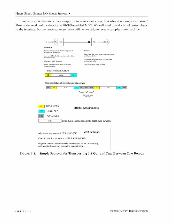
HIGH-SPEED SERIAL I/O MADE SIMPLE •
64 • Xilinx PRELIMINARY INFORMATION
So that is all it takes to define a simple protocol in about a page. But what about implementation? Most of the work will be done by an 8b/10b-enabled MGT. We will need to add a bit of custom logic to the interface, but no processor or software will be needed; not even a complex state machine.
FIGURE 4-8: Simple Protocol for Transporting 1.8 Gbits of Data Between Two Boards
SF Data EF IdleIDLE IDLE IDLE SFSF Data EF IDLEIDLE
Number of Idleswill vary
IDLE
SF
EF
Data 2048 Bytes encoded into 2048 8b10b data symbols
K28.5, K28.5
K28.0, D0.0
K29.7, K28.5
8B10B Assignments
TX RX12 bits at 150Mhz 12 bits at 150Mhz
Transmitter
Takes incoming parallel stream and places itin packets of 2048 bytes.
Uses an MGT to 8b10b encode, serialize data,and drive on wire.
Wire speed is 2.5 Gbits/sec
Inserts variable number of idle charactersbetween packets
Receiver
Takes incoming serial stream strips start flags,end flags and idles.
Converts 8 bit received data into 12bit dataand stores in a fifo.
Data is read from fifo at 150Mhz
SFSF Data EF
Basic Packet Structure
Representation of multiple packets on wire
MGT settingsAlignment sequence = K28.5, K28.5 (SF)
Clock Correction sequence = K29.7, K28.5 (IDLE)
Physical Details: Pre-emphasis, termination, AC or DC coupling,and amplitude can vary according to application.
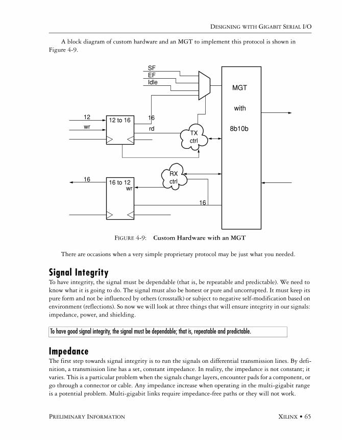
DESIGNING WITH GIGABIT SERIAL I/O
PRELIMINARY INFORMATION XILINX • 65
A block diagram of custom hardware and an MGT to implement this protocol is shown in Figure 4-9.
There are occasions when a very simple proprietary protocol may be just what you needed.
Signal IntegrityTo have integrity, the signal must be dependable (that is, be repeatable and predictable). We need to know what it is going to do. The signal must also be honest or pure and uncorrupted. It must keep its pure form and not be influenced by others (crosstalk) or subject to negative self-modification based on environment (reflections). So now we will look at three things that will ensure integrity in our signals: impedance, power, and shielding.
ImpedanceThe first step towards signal integrity is to run the signals on differential transmission lines. By defi-nition, a transmission line has a set, constant impedance. In reality, the impedance is not constant; it varies. This is a particular problem when the signals change layers, encounter pads for a component, or go through a connector or cable. Any impedance increase when operating in the multi-gigabit range is a potential problem. Multi-gigabit links require impedance-free paths or they will not work.
FIGURE 4-9: Custom Hardware with an MGT
To have good signal integrity, the signal must be dependable; that is, repeatable and predictable.
16 to 1216
wr
RXctrl
16
12 to 1612
wr16
SFEFIdle
TXctrl
rd
MGT
with
8b10b

HIGH-SPEED SERIAL I/O MADE SIMPLE •
66 • Xilinx PRELIMINARY INFORMATION
The transmission path should modeled, and connectors and cables finalized with CAD signal integrity tools before layout. Then, when we get the first prototypes, the impedance of the paths should be verified using time domain reflectometry (TDR). One hundred-ohm and 50-ohm transmis-sion lines are the most commonly used values. Some transceivers can adapt to either, and some may support only one. Fifty-ohm is definitely the most common approach in the 10 Gb/s range. If both 100-ohm and 50-ohm are available, connector and cable selection become a critical consideration.
PowerDelivering power is another crucial element of using multi-Gigabit transceivers. Most MGTs have multiple power supply needs.
Typical supplies are:• RX analog power • TX analog power• Analog ground• RX termination voltage• TX termination voltage• Digital power• Digital ground.
TDR: Time Domain Reflectometry
FIGURE 4-10: DCA Screen Capture

DESIGNING WITH GIGABIT SERIAL I/O
PRELIMINARY INFORMATION XILINX • 67
It is critical that both the analog transmit and receive power supplies, and the associated analog ground be extremely clean. As such, it is common for the MGT manufacturer to define that specific circuits to be used. This will almost always call for separate analog voltage regulators for each voltage, if not each MGT, and a passive power filter consisting of a capacitor and a ferrite bead.
FIGURE 4-11: Filters for MGT Power Supply
RX Analog
Voltage
TX Analog
Voltage
RX Termination
Voltage
Analog
Ground
TX Termination
Voltage
2.5 V
VTT
VTR

HIGH-SPEED SERIAL I/O MADE SIMPLE •
68 • Xilinx PRELIMINARY INFORMATION
The ferrite bead has a low impedance at low frequencies and a very high impedance at high fre-quencies (Figure 4-12).
FIGURE 4-12: Equivalent Circuit and Frequency Characteristics
[Equivalent Circuit]
[Impedance-Frequency Characteristics (typical)]
1000
800
600
400
200
01 10 100 1000Frequency [MHz]
R : Real Part (Resistive Portion) X : Imaginary part (Inductive Portion)
Z
X
Impe
danc
e [Ω
]
R
R(f)

DESIGNING WITH GIGABIT SERIAL I/O
PRELIMINARY INFORMATION XILINX • 69
The characteristics of the ferrite bead and capacitor are very important. Often, the manufacturer recommends a specific part. Sections taken from sample data sheets are given in Figure 4-13 and Figure 4-14.
In some MGTs (especially those in flip chip packages) the capacitor will be included inside the package of the part. In this case, often only the ferrite bead is needed. If a manufacturer recommends a specific circuit, it is normally best to follow the exact recommendations. One reason for this is that, in cases where multiple MGTs are in a common part, it is normal to require only a single linear regu-lator. And while we think of our filter circuit as filtering power supply noise from reaching our MGT,
FIGURE 4-13: Sample Data Sheet Portion
FIGURE 4-14: Sample Impedance Plots
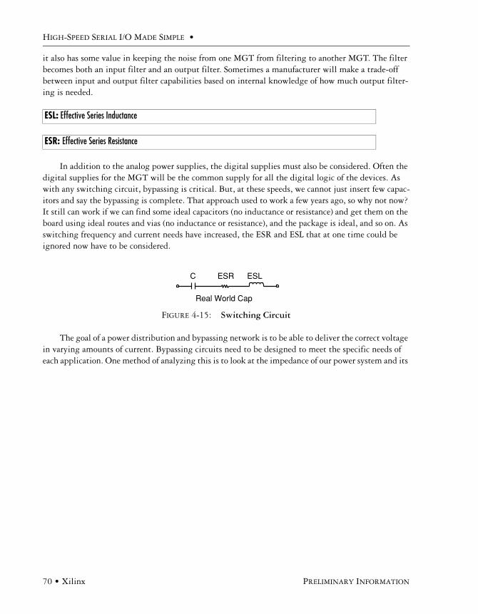
HIGH-SPEED SERIAL I/O MADE SIMPLE •
70 • Xilinx PRELIMINARY INFORMATION
it also has some value in keeping the noise from one MGT from filtering to another MGT. The filter becomes both an input filter and an output filter. Sometimes a manufacturer will make a trade-off between input and output filter capabilities based on internal knowledge of how much output filter-ing is needed.
In addition to the analog power supplies, the digital supplies must also be considered. Often the digital supplies for the MGT will be the common supply for all the digital logic of the devices. As with any switching circuit, bypassing is critical. But, at these speeds, we cannot just insert few capac-itors and say the bypassing is complete. That approach used to work a few years ago, so why not now? It still can work if we can find some ideal capacitors (no inductance or resistance) and get them on the board using ideal routes and vias (no inductance or resistance), and the package is ideal, and so on. As switching frequency and current needs have increased, the ESR and ESL that at one time could be ignored now have to be considered.
The goal of a power distribution and bypassing network is to be able to deliver the correct voltage in varying amounts of current. Bypassing circuits need to be designed to meet the specific needs of each application. One method of analyzing this is to look at the impedance of our power system and its
ESL: Effective Series Inductance
ESR: Effective Series Resistance
FIGURE 4-15: Switching Circuit
C ESR ESL
Real World Cap

DESIGNING WITH GIGABIT SERIAL I/O
PRELIMINARY INFORMATION XILINX • 71
associated frequency. Figure 4-16 shows the frequency response for three capacitors commonly recom-mended in standard applications.
Notice two main problems. One problem is the large impedance spikes between the values. If our system happens to need power supplied in that frequency range, we will have a problem. Part of
FIGURE 4-16: Impedance vs. Frequency for Improperly Selected Capacitors

HIGH-SPEED SERIAL I/O MADE SIMPLE •
72 • Xilinx PRELIMINARY INFORMATION
designing our bypassing circuit is to make sure these spikes are in areas not critical to our particular design. This can be accomplished by using different capacitors (Figure 4-17).
The other problem occurs at the upper frequency range. It first becomes difficult, and then impossible to find capacitors to cover the range. As the capacitor's value decreases, the associated stray inductance and resistance of the package cannot change proportionally to the capacitance, and there-fore the frequency response does not change much either. To get proper power distribution at the upper rates, we need to build our own capacitor using the power and ground planes. To do this effec-tively usually involves having adjacent power and ground planes. A typical stack-up would look like this (Figure 4-18)
FIGURE 4-17: Impedance vs. Frequency for Properly Selected Capacitors
FIGURE 4-18: Typical Stack-up
Four Values of Parallel Capacitors [ohms]
1.E-03
1.E-02
1.E-01
1.E+00
1.E-03 1.E-02 1.E-01 1.E+00 1.E+01 1.E+02 1.E+03
Frequency [MHz]
Impe
danc
e Z
(oh
ms)

DESIGNING WITH GIGABIT SERIAL I/O
PRELIMINARY INFORMATION XILINX • 73
Another important aspect of bypassing is placement. As a general rule, the larger the cap value, the less critical the placement. The smallest values want to go as near a power and ground pin as pos-sible. One way to do this that is often available when using MGTS inside FPGAs is to remove the trace and via of unused general IO to make room for the bypassing. This is shown in Figure 4-19.
ShieldingAny multi-gigabit signal needs to be isolated from interfering, and being interfered on, by other sig-nals, whether the signal is on a board, cable, or going through a connector. This is accomplished by isolation and shielding with connectors and cables. On PCBs, multi-gigabit signals should be isolated from other signals by using extra space, and should be isolated from parallel traces on other layers by ground or power planes.
Boards, Connectors, and CablesWhen designing a system that uses multi-gigabit serial streams, component selection and board design are critical. The wrong connector, a marginal stack-up, or the wrong PCB material can com-pletely ruin an MGT project.
Printed Circuit Board DesignDesigning a PCB for multi-gigabit operation is a challenge for even the best PCB designers. Differen-tial traces must be matched, geometry for impedance-controlled differential pairs must be adjusted as layers are added, and power distribution needs to be critically analyzed. And while there will be thou-sands of individual trade-offs and decisions, an overall list of issues can help. That list of issues might include the following:
• Material selection • Stack-up/board thickness • Power and ground planes • Differential pairs • Differential trace width and spacing • Vias • Space between pairs• Ground guards between pairs• Power layout.
FIGURE 4-19: Removing Trace and Via

HIGH-SPEED SERIAL I/O MADE SIMPLE •
74 • Xilinx PRELIMINARY INFORMATION
Material SelectionWhile FR-4 has become the standard board material for a number of years, some lower loss alterna-tives have become readily available. A general guideline is that for total trace length less than 20 inches and speed at or below 3.125 Gb/s, FR-4 may be acceptable. If we need longer traces or faster speed, we should seriously consider using a high-speed material such as ROGERS 3450.
Stack-up/Board ThicknessOnce we have selected a material, the next step will be to devise a general stack-up plan. This may change as the number of signal layers is determined, but we will need to keep our stack-up in mind throughout the processes. Do not forget to add an adjacent power and ground plane layer to improve bypassing.
Power and Ground PlanesWe need to think about how we are going to distribute all those special analog voltages. We may need to consider separate planes for each analog power. Isolating and filtering ground planes that are the ref-erence plane for the multi-gigabit signals might be a good idea. We could also consider eliminating the digital power supply plane from signal areas that operate at less than gigabit speed.
Differential PairsFor best results, we should run differential pairs tightly coupled and closely matched. Trace length matching is essential. In FR-4, a 100-mil (1 tenth of an inch) difference in trace length results in approximately 18 picoseconds of difference between the positive and negative signal. This is also enough skew to start causing problems. And, while a tenth of an inch may sound like a lot if we just use normal trace routing from one BGA to another, it is easy to end up with 300 - 400 mils of differ-ence. If our PCB tool has an auto-trace matching, we need to use it. In general, we will want 50 mils or less difference in differential trace lengths.
Differential Trace Width and SpacingThis will need to be worked out for each particular stack-up. The board foundry can be a valuable resource, but we need to make sure they know what they are doing. Some published guidelines recom-mend against letting the PCB vendor do these calculations. We need to make sure they are using a field solver tool to figure the width and spacing of tightly coupled pairs. Then we need to adjust our boards accordingly. One technique we definitely should not use is just choosing a close geometry and then letting the board foundry adjust the impedance with over- or under-etching. If we have a local, in-house field solving program and the expertise to use it, that is even better.
Sample geometry is shown in Figure 4-20 and Figure 4-21.
FIGURE 4-20: Sample Geometry: Microstrip Edge-Coupled Differential Pair
Trace Trace
Reference Plane
Dielectric
W2W1 S
H
W1 = 6.29 mil (0.160 mm)W2 = 6.29 mil (0.160 mm)S = 10 mil (0.254 mm)H = 5.0 mil (0.127 mm)Z01 = 55.3Z02 = 55.3Z0DIFF = 100Er = 4.3
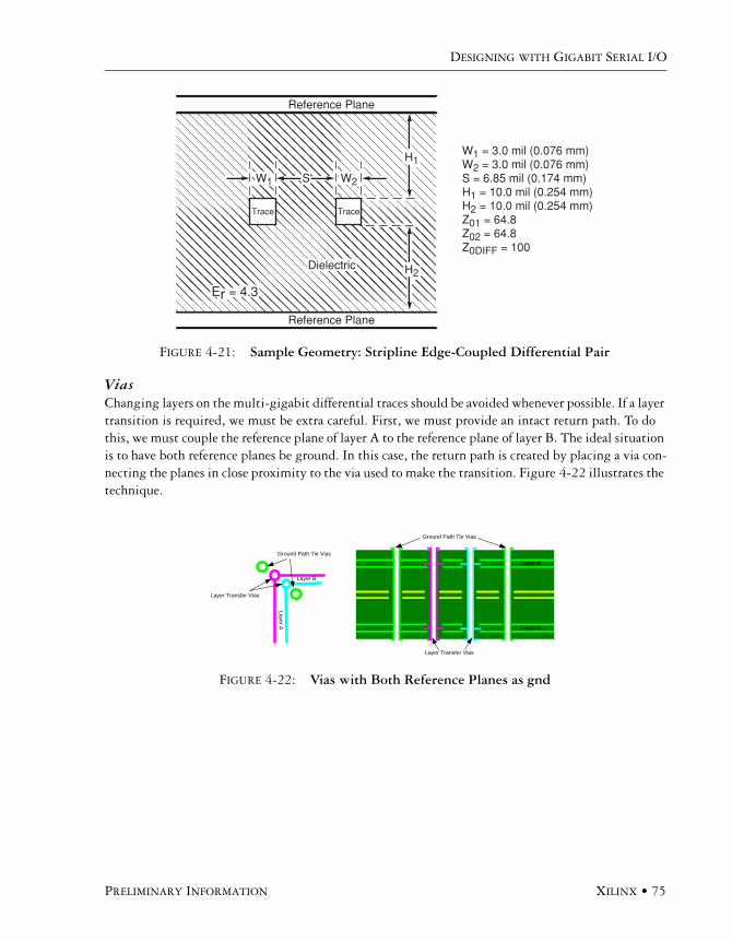
DESIGNING WITH GIGABIT SERIAL I/O
PRELIMINARY INFORMATION XILINX • 75
ViasChanging layers on the multi-gigabit differential traces should be avoided whenever possible. If a layer transition is required, we must be extra careful. First, we must provide an intact return path. To do this, we must couple the reference plane of layer A to the reference plane of layer B. The ideal situation is to have both reference planes be ground. In this case, the return path is created by placing a via con-necting the planes in close proximity to the via used to make the transition. Figure 4-22 illustrates the technique.
FIGURE 4-21: Sample Geometry: Stripline Edge-Coupled Differential Pair
FIGURE 4-22: Vias with Both Reference Planes as gnd
TraceTrace
Reference Plane
Reference Plane
Dielectric
W2W1 S
H2
H1W1 = 3.0 mil (0.076 mm)W2 = 3.0 mil (0.076 mm)S = 6.85 mil (0.174 mm)H1 = 10.0 mil (0.254 mm)H2 = 10.0 mil (0.254 mm)Z01 = 64.8Z02 = 64.8Z0DIFF = 100
Er = 4.3
Layer B
Layer A
Layer Transfer Vias
Ground Path Tie Vias
Layer Transfer Vias
Layer A
Layer B
Ground Path Tie Vias
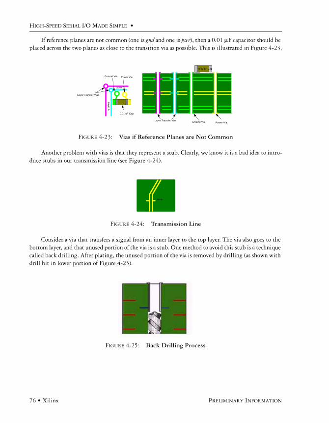
HIGH-SPEED SERIAL I/O MADE SIMPLE •
76 • Xilinx PRELIMINARY INFORMATION
If reference planes are not common (one is gnd and one is pwr), then a 0.01 μF capacitor should be placed across the two planes as close to the transition via as possible. This is illustrated in Figure 4-23.
Another problem with vias is that they represent a stub. Clearly, we know it is a bad idea to intro-duce stubs in our transmission line (see Figure 4-24).
Consider a via that transfers a signal from an inner layer to the top layer. The via also goes to the bottom layer, and that unused portion of the via is a stub. One method to avoid this stub is a technique called back drilling. After plating, the unused portion of the via is removed by drilling (as shown with drill bit in lower portion of Figure 4-25).
FIGURE 4-23: Vias if Reference Planes are Not Common
FIGURE 4-24: Transmission Line
FIGURE 4-25: Back Drilling Process
Power Via
0.01 uF Cap
Layer B
Layer A
Layer Transfer Vias
Ground Via
Power ViaGround Via
0.01 uF Cap
Layer Transfer Vias

DESIGNING WITH GIGABIT SERIAL I/O
PRELIMINARY INFORMATION XILINX • 77
Any design over 5 Gb/s should seriously consider back drilling vias (see Figure 4-26).
Space Between PairsIt is important to maintain a good amount of distance between differential pairs carrying multi-giga-bit signals and other traces. One general rule is that at least five times the space between the two sig-nals of the pair should be placed between adjacent pairs (Figure 4-27).
FIGURE 4-26: Back Drilled vs. Non-Back Drilled Channels
FIGURE 4-27: Space Between Pairs

HIGH-SPEED SERIAL I/O MADE SIMPLE •
78 • Xilinx PRELIMINARY INFORMATION
Ground guards between pairsAnother technique is to route a ground guard in parallel to the differential traces. Tying the guard plane back to the reference plane using a via in parallel to the trace often improves this shielding method (Figure 4-28).
Power layoutMany of the items discussed in the Powering MGT section have board layout implications as well. The placement of the ferrite beads (Figure 4-29) and capacitors that filter the analog power supplies rela-tive to the supply pins and the signal traces (Figure 4-30) must be carefully considered.
FIGURE 4-28: Ground Guards Between Pairs
FIGURE 4-29: Placement of Ferrite Beads
GN
D
GN
D

DESIGNING WITH GIGABIT SERIAL I/O
PRELIMINARY INFORMATION XILINX • 79
Connector SelectionOnly high-speed connectors should be used for multi-gigabit signals. Like everything else in the path, a high-speed connector has controlled impedance. While the connector impedance is never as contin-uous as a PCB trace, high-speed connectors are much better than normal connectors (Figure 4-31). Early high-speed connectors were designed for both single-ended and differential signals. The latest, fastest connectors are designed specifically for differential pairs. Here are a few examples of high-speed connectors:
• Gbx• VHDM-HSD• VHDM• HDM• High Density Plus• Z-PACK HM-Zd
FIGURE 4-30: Power Layout
Analog Power Filters
Large Bypass
MediumBypass
Small BypassNear Power Pins
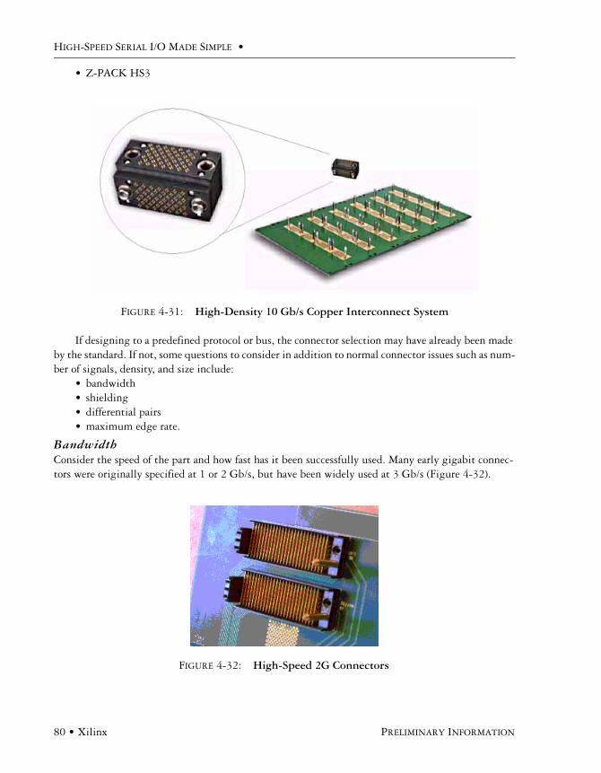
HIGH-SPEED SERIAL I/O MADE SIMPLE •
80 • Xilinx PRELIMINARY INFORMATION
• Z-PACK HS3
If designing to a predefined protocol or bus, the connector selection may have already been made by the standard. If not, some questions to consider in addition to normal connector issues such as num-ber of signals, density, and size include:
• bandwidth • shielding• differential pairs • maximum edge rate.
BandwidthConsider the speed of the part and how fast has it been successfully used. Many early gigabit connec-tors were originally specified at 1 or 2 Gb/s, but have been widely used at 3 Gb/s (Figure 4-32).
FIGURE 4-31: High-Density 10 Gb/s Copper Interconnect System
FIGURE 4-32: High-Speed 2G Connectors
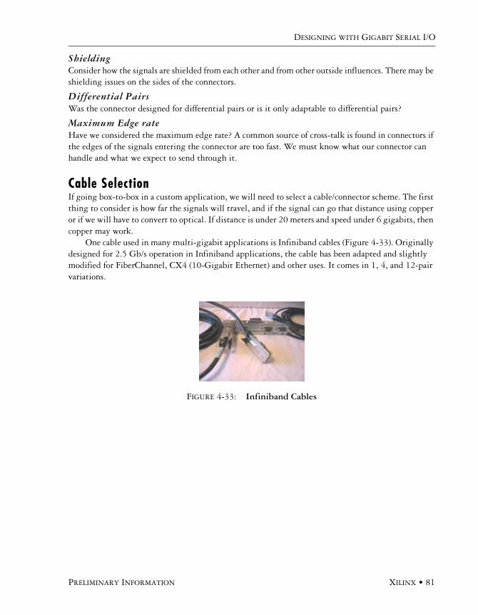
DESIGNING WITH GIGABIT SERIAL I/O
PRELIMINARY INFORMATION XILINX • 81
ShieldingConsider how the signals are shielded from each other and from other outside influences. There may be shielding issues on the sides of the connectors.
Differential PairsWas the connector designed for differential pairs or is it only adaptable to differential pairs?
Maximum Edge rateHave we considered the maximum edge rate? A common source of cross-talk is found in connectors if the edges of the signals entering the connector are too fast. We must know what our connector can handle and what we expect to send through it.
Cable SelectionIf going box-to-box in a custom application, we will need to select a cable/connector scheme. The first thing to consider is how far the signals will travel, and if the signal can go that distance using copper or if we will have to convert to optical. If distance is under 20 meters and speed under 6 gigabits, then copper may work.
One cable used in many multi-gigabit applications is Infiniband cables (Figure 4-33). Originally designed for 2.5 Gb/s operation in Infiniband applications, the cable has been adapted and slightly modified for FiberChannel, CX4 (10-Gigabit Ethernet) and other uses. It comes in 1, 4, and 12-pair variations.
FIGURE 4-33: Infiniband Cables
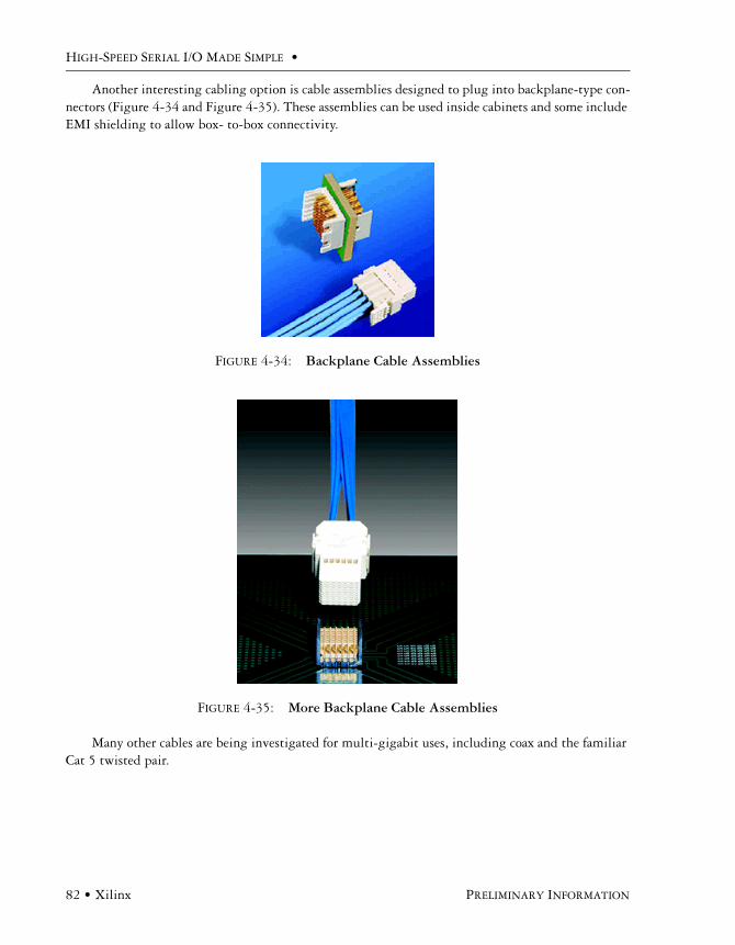
HIGH-SPEED SERIAL I/O MADE SIMPLE •
82 • Xilinx PRELIMINARY INFORMATION
Another interesting cabling option is cable assemblies designed to plug into backplane-type con-nectors (Figure 4-34 and Figure 4-35). These assemblies can be used inside cabinets and some include EMI shielding to allow box- to-box connectivity.
Many other cables are being investigated for multi-gigabit uses, including coax and the familiar Cat 5 twisted pair.
FIGURE 4-34: Backplane Cable Assemblies
FIGURE 4-35: More Backplane Cable Assemblies
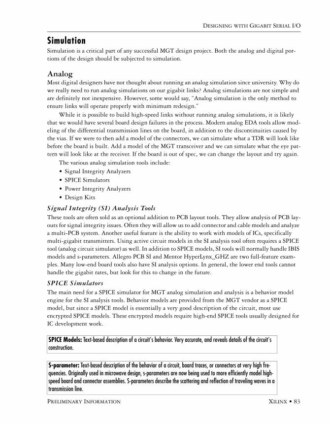
DESIGNING WITH GIGABIT SERIAL I/O
PRELIMINARY INFORMATION XILINX • 83
SimulationSimulation is a critical part of any successful MGT design project. Both the analog and digital por-tions of the design should be subjected to simulation.
AnalogMost digital designers have not thought about running an analog simulation since university. Why do we really need to run analog simulations on our gigabit links? Analog simulations are not simple and are definitely not inexpensive. However, some would say, “Analog simulation is the only method to ensure links will operate properly with minimum redesign.”
While it is possible to build high-speed links without running analog simulations, it is likely that we would have several board design failures in the process. Modern analog EDA tools allow mod-eling of the differential transmission lines on the board, in addition to the discontinuities caused by the vias. If we were to then add a model of the connectors, we can simulate what a TDR will look like before the board is built. Add a model of the MGT transceiver and we can simulate what the eye pat-tern will look like at the receiver. If the board is out of spec, we can change the layout and try again.
The various analog simulation tools include:• Signal Integrity Analyzers• SPICE Simulators• Power Integrity Analyzers• Design Kits
Signal Integrity (SI) Analysis ToolsThese tools are often sold as an optional addition to PCB layout tools. They allow analysis of PCB lay-outs for signal integrity issues. Often they will allow us to add connector and cable models and analyze a multi-PCB system. Another useful feature is the ability to work with models of ICs, specifically multi-gigabit transmitters. Using active circuit models in the SI analysis tool often requires a SPICE tool (analog circuit simulator) as well. In addition to SPICE models, SI tools will normally handle IBIS models and s-parameters. Allegro PCB SI and Mentor HyperLynx_GHZ are two full-feature exam-ples. Many low-end board tools also have SI analysis options. In general, the lower end tools cannot handle the gigabit rates, but look for this to change in the future.
SPICE SimulatorsThe main need for a SPICE simulator for MGT analog simulation and analysis is a behavior model engine for the SI analysis tools. Behavior models are provided from the MGT vendor as a SPICE model, but since a SPICE model is essentially a very good description of the circuit, most use encrypted SPICE models. These encrypted models require high-end SPICE tools usually designed for IC development work.
SPICE Models: Text-based description of a circuit's behavior. Very accurate, and reveals details of the circuit's construction.
S-parameter: Text-based description of the behavior of a circuit, board traces, or connectors at very high fre-quencies. Originally used in microwave design, s-parameters are now being used to more efficiently model high-speed board and connector assemblies. S-parameters describe the scattering and reflection of traveling waves in a transmission line.
HIGH-SPEED SERIAL I/O MADE SIMPLE •
84 • Xilinx PRELIMINARY INFORMATION
Example tools include H-SPICE from Synopsys and ICX/Edo from Mentor. These high-end SPICE tools tend to be expensive. Encrypted capabilities may appear on the low-end tools in thefuture. Although SPICE is a powerful tool and there is a lot more we could do with it, but using a signal integrity analysis tool combined with SPICE is much more efficient. Note that an old copy of P-SPICE will not work for this analysis.
Power Integrity ToolsThese tools help design the power delivery (bypassing, filtering, and so on) system. Many are added-on to signal integrity analysis tools. These tools provide the same type of functionality for power sys-tems as the SI tools do for signals. A much less powerful and more affordable help on a portion of the power problem can be found in tools like UltraCAD's ESR and Bypass Capacitor Calculator that help pick capacitors for specific bypassing needs.
Design KitsOften a SERDES vendor and a signal integrity tool vendor will work together and provide reference materials to speed up the process of doing the analog simulations. The kits usually consist of a generic project that set up and ready to use. These can be opened in the SI tool so that we can start discovering the tools and SERDES capabilities. Once we are familiar with the general idea, we can begin replacing the pre-designed boards and connectors for our own. Since some of these tools have steep learning curves, this can be a valuable asset.
We may have to pick our analog simulation tools after we have a SERDES vendor. It is rather common to find simulation models or design kits available for only one particular tool set. This tends to improve with time, but it is something to remember.
DigitalWhile the analog simulation requirements of multi-gigabit links may force us into a completely new world of EDA tools, the digital end of it will be much less of an impact. There are, however, still a few things we need to consider.
First, many MGT behavior models come in a special encrypted format. These are complex cores and very valuable intellectual property (IP). As such, the vendors want to protect their property and will usually only release in an IP-safe format. The most popular format is called smart models or swift. Basically, the model is encrypted in a way that the simulator can read it and the user cannot. Internal nodes and hierarchy are not visible to the user; the user can only see the inputs and outputs of the model.
Two issues can arise with smart models and swift. First, our simulator must support them (some low end tools commonly used for FPGA simulations do not), and, second, we have to get the tools set up to use them, and that normally requires at least some effort.
The other problem with digital simulations of MGTs can be simulation speed. Our digital logic will most likely be running in the 100-300 MHz range. We can adjust our time-scale of the simula-
IBIS Models: Text-based description of a circuit's behavior. Adequately accurate at frequencies below 1 GHz. Does not reveal construction details of the circuit.

DESIGNING WITH GIGABIT SERIAL I/O
PRELIMINARY INFORMATION XILINX • 85
tion in the single-digit nanosecond range. But if we add a wire speed model of an MGT, we suddenly have a signal that transitions 20+ times faster than the previous fastest signal (Figure 4-36).
The time scale of the simulation must be adjusted, and that can slow things down considerably. Even screen redraws when these signals are displayed can become noticeably slower. There are some things we can do to lessen the impact. One is just to be aware that it is going to be a problem and opti-mize our simulations around the fact that these fast signals are a part of our design. The other thing to keep in mind is that many MGT models have a parallel in and out port. If we use this in most of our testbenches and create a small test suite that actually runs at the full data rate, the MGTs will have a much smaller impact on overall verification time. A diagram showing the approach is shown in Figure 4-37.
FIGURE 4-36: MGT Simulation
FIGURE 4-37: Block Diagram of Two Different Testbenches
TestBench
Logic MGT
Logic MGT
TestBench
Logic MGT
Logic MGT
Full function simulations including gigabit signals.Use this for verifying functionality related to MGTFor example simulating slightly differentreference clocks to check clock correction.
A parallel interface replaces the gigabit seriallinks. Makes for faster simulations but somefunctionality isn't there. Use this mode for thebulk of the verification of the interface logic.
HIGH-SPEED SERIAL I/O MADE SIMPLE •
86 • Xilinx PRELIMINARY INFORMATION
One Last Suggestion on Digital SimulationsWe must make sure our testbench addresses the problems that can result from different clocks, such as check all variations of clock correction and channel bonding if they are used. Clock correction that is malfunctioning will stop a project the first day the project arrives at the prototype lab.
Test and MeasurementIn the prototype phase of our project, MGT test and measurement considerations will require the use of some specialized test equipment to make specific measurements to ensure our project will operate as we anticipate.
Sampling Oscilloscopes and Digital Communication AnalyzersPerhaps the single most important piece of equipment for gigabit debug is a sampling oscilloscope (or just “scope”). A sampling scope is a bit different than a normal, or analog, scope or a digital storage scope. An analog scope works by directly applying the signal under study to the vertical axis of the electron beam that moves across a cathode ray tube (CRT) display, creating a trace that defines the shape of the actual signal. A digital storage scope converts the incoming signal to digital samples that are stored and then used to “recreate” the signal on a display. The sampling scope also digitizes the incoming information and stores it.
The sampling scope is different than an analog or digital storage scope in that it can be used to analyze signals that are extremely fast. In order to capture signals faster than the analog-to-digital con-verters (ADCs) can operate, the sampling scope captures only a few samples of each period. Moving the sampling each time allows it to capture enough signals to represent a repetitive signal. If a signal is very repetitive (like alternating ones and zeros), the actual waveform will be seen. In most cases, the sampling scope creates an eye pattern. In addition to the data input, a sampling scope has a clock input. This is a reference signal from which the scope can sample. This input can usually be a clock running at the wire rate or a division of the rate. Often, a rate/20 clock is acceptable. Figure 4-38
Sampling Scope: Digitizes the information and stores it. To capture signals faster than the analog-to-digital con-verters can go, the scope captures only a few samples of each period. Moving the sampling each time allows it to capture enough signals to represent a repetitive signal.
Digital Storage Scope: Converts the incoming signal to digital samples that are stored and then used to recreate the signal on a display.
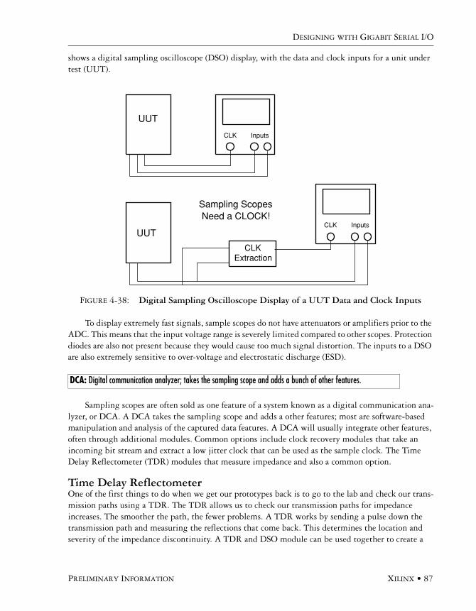
DESIGNING WITH GIGABIT SERIAL I/O
PRELIMINARY INFORMATION XILINX • 87
shows a digital sampling oscilloscope (DSO) display, with the data and clock inputs for a unit under test (UUT).
To display extremely fast signals, sample scopes do not have attenuators or amplifiers prior to the ADC. This means that the input voltage range is severely limited compared to other scopes. Protection diodes are also not present because they would cause too much signal distortion. The inputs to a DSO are also extremely sensitive to over-voltage and electrostatic discharge (ESD).
Sampling scopes are often sold as one feature of a system known as a digital communication ana-lyzer, or DCA. A DCA takes the sampling scope and adds a other features; most are software-based manipulation and analysis of the captured data features. A DCA will usually integrate other features, often through additional modules. Common options include clock recovery modules that take an incoming bit stream and extract a low jitter clock that can be used as the sample clock. The Time Delay Reflectometer (TDR) modules that measure impedance and also a common option.
Time Delay ReflectometerOne of the first things to do when we get our prototypes back is to go to the lab and check our trans-mission paths using a TDR. The TDR allows us to check our transmission paths for impedance increases. The smoother the path, the fewer problems. A TDR works by sending a pulse down the transmission path and measuring the reflections that come back. This determines the location and severity of the impedance discontinuity. A TDR and DSO module can be used together to create a
FIGURE 4-38: Digital Sampling Oscilloscope Display of a UUT Data and Clock Inputs
DCA: Digital communication analyzer; takes the sampling scope and adds a bunch of other features.
CLK Inputs
UUT
UUTUUT
CLK Inputs
CLKExtraction
Sampling ScopesNeed a CLOCK!
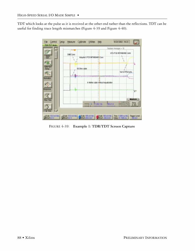
HIGH-SPEED SERIAL I/O MADE SIMPLE •
88 • Xilinx PRELIMINARY INFORMATION
TDT which looks at the pulse as it is received at the other end rather than the reflections. TDT can be useful for finding trace length mismatches (Figure 4-39 and Figure 4-40).
FIGURE 4-39: Example 1: TDR/TDT Screen Capture

DESIGNING WITH GIGABIT SERIAL I/O
PRELIMINARY INFORMATION XILINX • 89
Eye PatternsWe have already mentioned eye patterns several times. It is almost impossible to talk about high-speed serial streams without talking about eye patterns. An eye pattern is a natural consequence of the way a sampling scope works. An eye pattern occurs when we take snapshots of the exact same duration of a waveform of random bits, then superimpose the sequences (Figure 4-41).
FIGURE 4-40: Example 2: TDR/TDT Screen Capture
Eye Pattern: Common waveform viewed on digital sampling scopes. It is an indication of the quality of the signal. Jitter, impedance matching, and amplitude can all be characterized through eye patterns.

HIGH-SPEED SERIAL I/O MADE SIMPLE •
90 • Xilinx PRELIMINARY INFORMATION
We can see the same thing with our digital storage scope if we turn up the persistence on a ran-dom bit stream. As the signal quality decreases, the pattern begins to resemble eyes staring back at us, hence the name eye pattern (Figure 4-42 and Figure 4-43).
FIGURE 4-41: Eye Pattern Construction
FIGURE 4-42: Eye Pattern After an FR-4 Trace
Identical duration portions ofthe signal are superimposedon top of each other to formthe eye pattern.

DESIGNING WITH GIGABIT SERIAL I/O
PRELIMINARY INFORMATION XILINX • 91
By analyzing the eye pattern, we can discover much about the signal and the path it is traveling. The height and width of the eye shape correspond to the ability of a receiver to receive the signal. Often a receiver will have a published eye mask. If the eye pattern is within the mask, the receiver can detect the signal (Figure 4-44).
The width of the fill (cross over) in between the eyes is a representation of the jitter of the system. Other details, such as too little or too much pre-emphasis and impedance mismatches that are not
FIGURE 4-43: Eye Pattern Colors
FIGURE 4-44: Eye Mask Drawing
Wide Crossing indicateslots of jitter
Multiple distinctamplitudes, some ofthe jitter may be fromISI
One and two bitsequences are notmaking it to fullamplitude

HIGH-SPEED SERIAL I/O MADE SIMPLE •
92 • Xilinx PRELIMINARY INFORMATION
symmetrical on both sides of the differential pair can be identified through anomalies in the shape of the eye (Figure 4-45).
Another important aspect of eye patterns is color. Most modern equipment uses color as a way of signifying intensity. The darker or “hotter” the color, the more data samples have landed at that loca-tion. In this eye pattern (Figure 4-46), the orange shows many data samples (“hits”) and the green is just a few “hits.”
FIGURE 4-45: Eye Pattern Anomalies
FIGURE 4-46: Eye Pattern Colors
Unusual dip/bumppossible impedanceproblem
Right and Left sides of eye notsymmetrical indication of diff pairimpedance, length of coupling problems

DESIGNING WITH GIGABIT SERIAL I/O
PRELIMINARY INFORMATION XILINX • 93
Another term associated with eye patterns is eye mask. This is simply a definition of how good or open an eye pattern needs to be for a receiver to operate correctly. An eye mask might look something like this (Figure 4-47).
JitterWe have already used the term jitter and we know it is related to the width of the line between indi-vidual eyes of an eye pattern. When we are in the lab debugging a multi-gigabit link, we will want a good understanding of what jitter is, where it comes from, and what it can affect.
Mathematically, we could talk about jitter as a variation in the period of our signal. For example, if we had a sine wave clock, we could define a perfect zero jitter clock as:
cos(w(t))
Then a description of the jittery signal would be:
cos(w(t) + j(t))
where j(t) is a function describing the jitter. Jitter is often categorized into two types: deterministic and random:
• Random jitter: The component of the jitter resulting from differential and common mode stochastic noise processes such as power supply noise and thermal noise. Also known as rj, RJ, and called indeterministic jitter.
• Deterministic jitter: The component of the jitter attributable to specific patterns or events. Includes jitter resulting from sources such as asymmetric rise/fall times, inter-symbol interference, power-supply feed through, oscillator wand, and cross-talk from other signals. Often abbreviated as DJ or dj.
FIGURE 4-47: Eye Mask Pattern
Jitter: The difference between the ideal zero crossing and the actual zero crossing.
100
87.5
100
Z2 (mV)
800
800
800
Z1 (mV)
0.5000.3750.3560.2311.25 (802.3z)
0.5000.3250.3800.2052.5 (Infiniband)
0.4250.3000.3050.1803.125 (XAUI)
Y2 (UI)Y1 (UI)X2 (UI)X1 (UI)Data rate (Gbps)
Y1 0 1 (1–Y2) Y2
Normalized bit time (UI)
Signal amplitude (mV)
–Z2
–Z1
0
Z2
Z1
X1 X2 (1–X2) (1–X1)
(1–Y1)

HIGH-SPEED SERIAL I/O MADE SIMPLE •
94 • Xilinx PRELIMINARY INFORMATION
When investigating why a multi-gigabit link is not working, the most likely problem is exces-sive jitter. It is a good idea to get a feel for how much jitter there is on the incoming signal of the receivers and compare that to the specification of the receiver. It is also a good idea to check the ampli-tude/eye height while we are looking. If everything looks acceptable, jitter is most likely not the prob-lem.
Generators and Bit Error TestersOther useful items to have in the lab are pattern and clock generators and bit error testers. These low jitter generators are useful for developing test patterns and checking bit error rates. Here is one way these might be used (Figure 4-48).
FIGURE 4-48: Generators and Bit Error Testers
High-speed Clock Generator
BREFCLK Clock Generator
Stimulus System Infinium DCA Scope
Agilent 86100AHFS9003
HP8648D
HP8648D
BERT
Attenuators
TempForcingUnit
HP 71603B
MicrostripBoard
ML321Board
Pattern Generator
Error Detector
Clock Source
"3.2 Gb/s"
"160 MHz"
"160 MHz"
PhaseLockOut
ClockOut
PhaseLockOut
PhaseLock
In
ClockOut
ClockOut
ClockOut
ClockIn
ClockIn
ClockIn
CLK+ CLK- CLK+ CLK-
ExternalTrigger
Channel 1
Channel 2
Channel 1
Channel 2
InN InP
OutN OutP
TXP
RXP
RXN
TXN BREFCLK
DataIn
ModIn

DESIGNING WITH GIGABIT SERIAL I/O
PRELIMINARY INFORMATION XILINX • 95
Another type of diagram that is often associated with serial links is the bathtub curve (Figure 4-49).
The bathtub curve is a plot that shows the bit error rate relative to sampling position within the unit interval. The bottom of the curve is not zero, but however close to zero the testing stopped, nor-mally somewhere in the 10-12 to 10-16 range. The upper limit is a 100% bit error rate or 1. A bit error tester is often used to generate the bathtub curves. Under some circumstances, a relationship between
FIGURE 4-49: Bathtub Curve
1 UI
1E0
1E -16
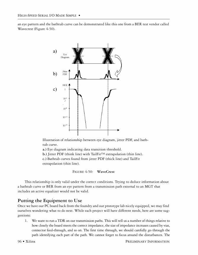
HIGH-SPEED SERIAL I/O MADE SIMPLE •
96 • Xilinx PRELIMINARY INFORMATION
an eye pattern and the bathtub curve can be demonstrated like this one from a BER test vendor called Wavecrest (Figure 4-50).
This relationship is only valid under the correct conditions. Trying to deduce information about a bathtub curve or BER from an eye pattern from a transmission path external to an MGT that includes an active equalizer would not be valid.
Putting the Equipment to UseOnce we have our PC board back from the foundry and our prototype lab nicely equipped, we may find ourselves wondering what to do next. While each project will have different needs, here are some sug-gestions:
1. We want to run a TDR on our transmission paths. This will tell us a number of things relative tohow closely the board meets the correct impedance, the size of impedance increases caused by vias,connector feed-through, and so on. The first time through, we should carefully go through thepath identifying each part of the path. We cannot forget to focus around the disturbances. The
FIGURE 4-50: WaveCrest
Illustration of relationship between eye diagram, jitter PDF, and bath-tub curve. a.) Eye diagram indicating data transition threshold. b.) Jitter PDF (think line) with TailFit™ extrapolation (thin line). c.) Bathtub curves found from jitter PDF (thick line) and TailFit extrapolation (thin line).

DESIGNING WITH GIGABIT SERIAL I/O
PRELIMINARY INFORMATION XILINX • 97
connectors, vias, and so on, will often look like a single disturbance until we focus in. It us a goodidea to verify where we are looking. This can be done by pressing a finger down on the vias orpads. The capacitance of a finger changes the impedance slightly and we can normally see that onthe display. Comparing our actual TDR to simulated ones we did with the signal integrityanalysis tools may also provide some valuable insight.
2. The next thing to do is to look at the eye pattern as close to the pins of the receiver as possible.Look at the eye compared to the receiver specifications. Is the jitter within tolerance? Is the eyeheight/amplitude correct? If all looks good, it is time to try the link. If not, we need to check outthe debug hints below.
Multi-gigabit Debug HintsDebugging your multi-gigabit design can sometimes be a challenge. Some debugging hints you can use cover the following areas:
• Low Signal Amplitude• Low Eye Pattern Height• Excessive Jitter• Using SI Tools• A Final Debugging Hint
Low Signal Amplitude at the Receive PinsIf our amplitude is too low, we may be able to crank up the voltage of the output driver. If we cannot fix the problem with output drive, we have too much loss in our boards and connectors; at this point we will really wish we had done those analog simulations because we are looking at a board redesign. Before we concede, we will want to make sure it is not a test setup problem or a manufacturing defect. Check all connections, part numbers, component values, and so on. We may also want to check the amplitude at various points along the path to get a feel for where the loss is occurring.
Low Eye Pattern HeightIf the overall amplitude is high enough but the height of the eye pattern is small, then some bits are getting high enough, but others are not. This is often a result of a difference in gain/attenuation of the path or transmitter at some frequencies. Usually the easiest thing to try is to check our pre-emphasis settings. It could be that we are just not getting high enough on single bit transitions. If we have an equalizer or equalized cable in the path, we will want to check and make sure they are the correct val-ues. If we can adjust the equalization, we should try that.
Excessive Jitter for ReceiveThis is the most common problem of non-working links. Low eye pattern height will often accompany jitter problems, so all of the suggestions for low eye pattern height apply here as well. If it is not a pre-emphasis problem and the associated jitter from internal signal integrity or our equalizer settings, it is time to start looking for other sources of jitter. Some likely candidates are:
• Power supply problems, feed through, and noise• Cross-talk • Asymmetrical rise/fall times• Common mode problems from unmatched differential traces• Oscillator wander or jitter.Determining jitter sources can be challenging. We will want to use our best lab techniques, good
notes, and so on, to systematically divide and conquer. We will also want to be familiar with every fea-
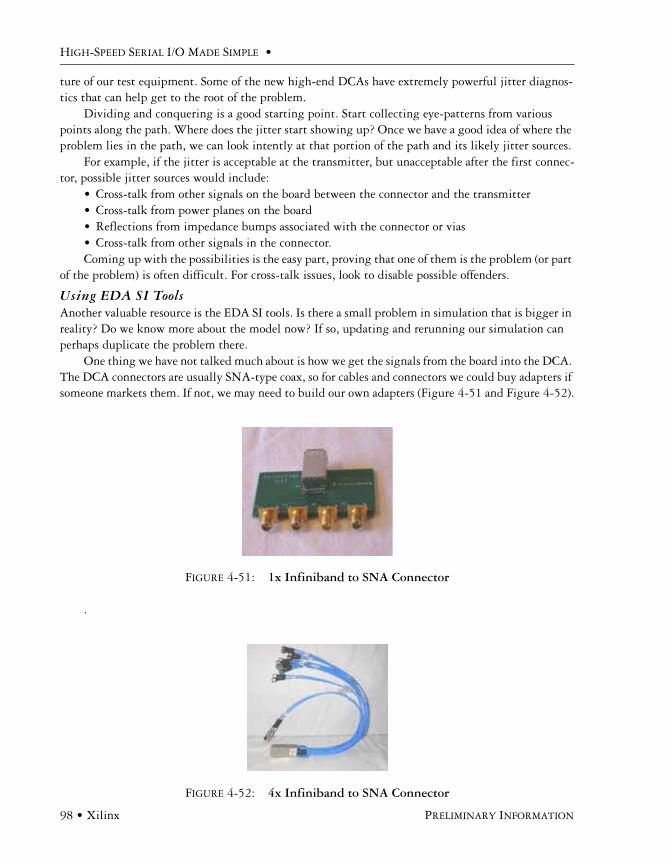
HIGH-SPEED SERIAL I/O MADE SIMPLE •
98 • Xilinx PRELIMINARY INFORMATION
ture of our test equipment. Some of the new high-end DCAs have extremely powerful jitter diagnos-tics that can help get to the root of the problem.
Dividing and conquering is a good starting point. Start collecting eye-patterns from various points along the path. Where does the jitter start showing up? Once we have a good idea of where the problem lies in the path, we can look intently at that portion of the path and its likely jitter sources.
For example, if the jitter is acceptable at the transmitter, but unacceptable after the first connec-tor, possible jitter sources would include:
• Cross-talk from other signals on the board between the connector and the transmitter• Cross-talk from power planes on the board• Reflections from impedance bumps associated with the connector or vias• Cross-talk from other signals in the connector.Coming up with the possibilities is the easy part, proving that one of them is the problem (or part
of the problem) is often difficult. For cross-talk issues, look to disable possible offenders.
Using EDA SI ToolsAnother valuable resource is the EDA SI tools. Is there a small problem in simulation that is bigger in reality? Do we know more about the model now? If so, updating and rerunning our simulation can perhaps duplicate the problem there.
One thing we have not talked much about is how we get the signals from the board into the DCA. The DCA connectors are usually SNA-type coax, so for cables and connectors we could buy adapters if someone markets them. If not, we may need to build our own adapters (Figure 4-51 and Figure 4-52).
.
FIGURE 4-51: 1x Infiniband to SNA Connector
FIGURE 4-52: 4x Infiniband to SNA Connector

DESIGNING WITH GIGABIT SERIAL I/O
PRELIMINARY INFORMATION XILINX • 99
Looking at signals on the PC board is more difficult. If we happen to be using AC coupling, we can often remove the coupling capacitors and solder on small wires. We can also remove parts and sol-der wires onto the pads.
This can get a bit messy and stress our prototypes. It is a good idea to always plan that several of the prototypes will be destroyed for test and verification. We may even want to have some prototypes specially built with certain parts missing.
A Final Debugging HintThere is one last thing to keep in mind when debugging gigabit links. There are two main parts to the link, the physical portion and the protocol. All the above suggestions have applied to the physical link and have assumed that everything is either acceptable with the protocol level, or it has been eliminated from testing by use of pattern and clock generators. Digital simulations should have most of the pro-tocol bugs worked out before we ever get to prototype, but there is still some room for overlap. For example, if we are getting errors in our bit stream, but our receive input jitter looks great, the problem may actually be a clock correction problem.
InteroperabilityWhen designing to a specific standard, chances are we will need to be compatible with other products. Or perhaps we just need to interface with a previous version of a custom application and the older ver-sion uses a different SERDES vendor. There are a few things to look for to make inter operability a real-ity.
Protocol LevelWhen interfacing to another system running the “same” protocol, expect to have problems. These pro-tocols are so complex that there are bound to be different interpretations of the specification. Submit-ting our device to an independent verification lab is one approach to make certain our interpretation of the specification is correct. Purchasing the protocol engine design or software may also be a benefit to inter operability. If we are interfacing to a custom protocol, we may want to try to use the same source code if possible.
FIGURE 4-53: Wired Prototype

HIGH-SPEED SERIAL I/O MADE SIMPLE •
100 • Xilinx PRELIMINARY INFORMATION
ElectricalOn the physical end, things will be a bit simpler. If we are using a standard protocol, most things like connectors, levels, and so on, will have been defined. If it is a custom application, the details of the physical interface may not have been as well defined. We must keep three items in mind; level, cou-pling, and termination.
We will want to be transmitting and receiving at the same level as the equipment to which we are interfacing. We will also need to determine how we are going to be coupled. If both SERDES are sim-ilar or have a common termination voltage, we may be able to DC couple. This eliminates the AC cou-pling capacitor and some problems that they can bring. If a common DC coupling is not practical, AC coupling can solve the problem (Figure 4-54).
Other ResourcesAt this point you might be excited and ready to get started with your design, and ready to start using this new technology. You must be a working design engineer. You could also be excited, but worried. You might ask, “Can we ramp up quick enough? Will our normal board foundry handle the job? Can we get enough money for the new equipment?” Obviously, you are an engineering manager. If you are somewhere in between, chances are you are a veteran design engineer who has been around long enough to know when to be concerned. Do not fret too much, there is help available.
Design ServicesLike most everything in the world of engineering, we can simply hire someone who already has the experience to do the work for us. If we are thinking about doing this, we need to be certain to consider tools and flows. Does the design company have signal integrity tools? Which ones? Will they work with our board design package? Often, the best design consultant can not only give us a fast start on the first project, but they can educate our team in the process so they can handle the next project on their own.
Testing CentersIf the budget for test and measurement equipment is a big problem, consider using a vendor or third party testing center. Since the equipment is expensive, some SERDES vendors have established labs that their customers can use to verify and debug their hardware. These labs are usually nicely equipped and often offer an option to provide an experienced multi-gigabit engineer or technician for help. Some third parties have set up similar labs as a regular business. A third trend shows that major research facilities of leading edge companies have recently begun renting space on a short-term basis.
FIGURE 4-54: AC and DC Coupling Diagrams
VTTVTT
AC Coupled MGTS
VTT1 VTT2
Termination voltage &signal levels can be
different
VTT VTT
VTT
Termination voltage &signal levels must be
identical
DC Coupled MGTS

DESIGNING WITH GIGABIT SERIAL I/O
PRELIMINARY INFORMATION XILINX • 101
These labs are already equipped for advanced research, and often have all the equipment for multi-gigabit lab work as well.
Development PlatformsAnother development resource is predesigned prototype boards. These are available from many of the SERDES vendors and third parties. From starting early work on the prototype, acting as a poor man's signal generator, or just letting the team get acquainted with the new DCA, these boards are usually reasonably priced and can be a valuable asset.

HIGH-SPEED SERIAL I/O MADE SIMPLE •
102 • Xilinx PRELIMINARY INFORMATION

PRELIMINARY INFORMATION XILINX • 103
CHAPTER 5
Xilinx—Your Design Partner
Additional design resources from Xilinx
Serial I/O Design ConsiderationsWe have looked at the history, the technology, and the real-world design considerations of a successful Multi-Gigabit Transceiver (MGT) project. This information provides the technical background neces-sary to begin effective serial input/output (I/O) design. In addition, Xilinx provides additional infor-mation that can help you use multi-gigabit serial in your I/O designs.
One Stop Serial I/O Web PortalXilinx provides a very powerful technical website with single click links to more information about Intellectual Property cores, reference designs, white papers, Signal Integrity (SI) and PCB design tools,

HIGH-SPEED SERIAL I/O MADE SIMPLE •
104 • Xilinx PRELIMINARY INFORMATION
boards, education services, and so on. The URL to bookmark is http://www.xilinx.com/serialsolution/.
FIGURE 5-1: High-Speed Serial Solutions Website
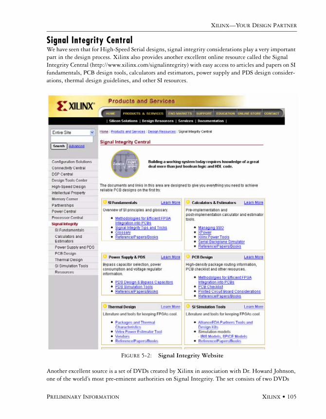
XILINX—YOUR DESIGN PARTNER
PRELIMINARY INFORMATION XILINX • 105
Signal Integrity CentralWe have seen that for High-Speed Serial designs, signal integrity considerations play a very important part in the design process. Xilinx also provides another excellent online resource called the Signal Integrity Central (http://www.xilinx.com/signalintegrity) with easy access to articles and papers on SI fundamentals, PCB design tools, calculators and estimators, power supply and PDS design consider-ations, thermal design guidelines, and other SI resources.
Another excellent source is a set of DVDs created by Xilinx in association with Dr. Howard Johnson, one of the world’s most pre-eminent authorities on Signal Integrity. The set consists of two DVDs
FIGURE 5-2: Signal Integrity Website
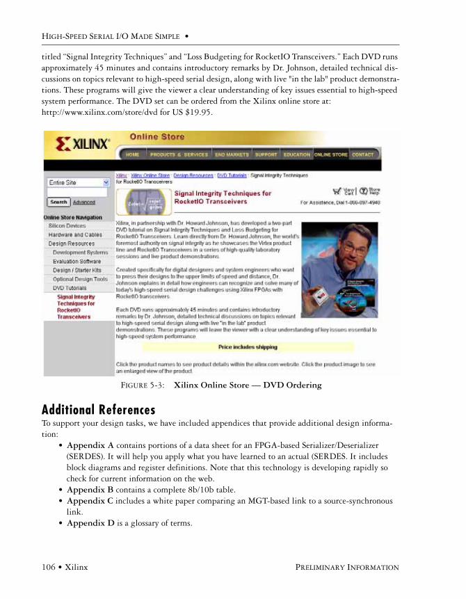
HIGH-SPEED SERIAL I/O MADE SIMPLE •
106 • Xilinx PRELIMINARY INFORMATION
titled “Signal Integrity Techniques” and “Loss Budgeting for RocketIO Transceivers.” Each DVD runs approximately 45 minutes and contains introductory remarks by Dr. Johnson, detailed technical dis-cussions on topics relevant to high-speed serial design, along with live "in the lab" product demonstra-tions. These programs will give the viewer a clear understanding of key issues essential to high-speed system performance. The DVD set can be ordered from the Xilinx online store at:http://www.xilinx.com/store/dvd for US $19.95.
Additional ReferencesTo support your design tasks, we have included appendices that provide additional design informa-tion:
• Appendix A contains portions of a data sheet for an FPGA-based Serializer/Deserializer (SERDES). It will help you apply what you have learned to an actual (SERDES. It includes block diagrams and register definitions. Note that this technology is developing rapidly so check for current information on the web.
• Appendix B contains a complete 8b/10b table.• Appendix C includes a white paper comparing an MGT-based link to a source-synchronous
link. • Appendix D is a glossary of terms.
FIGURE 5-3: Xilinx Online Store — DVD Ordering
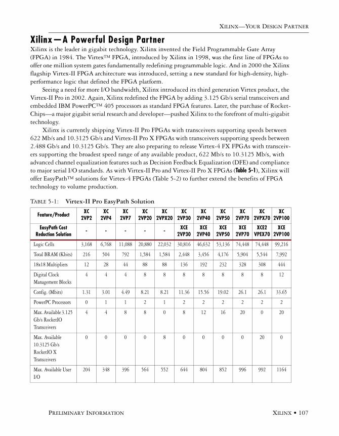
XILINX—YOUR DESIGN PARTNER
PRELIMINARY INFORMATION XILINX • 107
Xilinx—A Powerful Design PartnerXilinx is the leader in gigabit technology. Xilinx invented the Field Programmable Gate Array (FPGA) in 1984. The Virtex™ FPGA, introduced by Xilinx in 1998, was the first line of FPGAs to offer one million system gates fundamentally redefining programmable logic. And in 2000 the Xilinx flagship Virtex-II FPGA architecture was introduced, setting a new standard for high-density, high-performance logic that defined the FPGA platform.
Seeing a need for more I/O bandwidth, Xilinx introduced its third generation Virtex product, the Virtex-II Pro in 2002. Again, Xilinx redefined the FPGA by adding 3.125 Gb/s serial transceivers and embedded IBM PowerPC™ 405 processors as standard FPGA features. Later, the purchase of Rocket-Chips—a major gigabit serial research and developer—pushed Xilinx to the forefront of multi-gigabit technology.
Xilinx is currently shipping Virtex-II Pro FPGAs with transceivers supporting speeds between 622 Mb/s and 10.3125 Gb/s and Virtex-II Pro X FPGAs with transceivers supporting speeds between 2.488 Gb/s and 10.3125 Gb/s. They are also preparing to release Virtex-4 FX FPGAs with transceiv-ers supporting the broadest speed range of any available product, 622 Mb/s to 10.3125 Mb/s, with advanced channel equalization features such as Decision Feedback Equalization (DFE) and compliance to major serial I/O standards. As with Virtex-II Pro and Virtex-II Pro X FPGAs (Table 5-1), Xilinx will offer EasyPath™ solutions for Virtex-4 FPGAs (Table 5-2) to further extend the benefits of FPGA technology to volume production.
TABLE 5-1: Virtex-II Pro EasyPath Solution
Feature/Product XC2VP2
XC2VP4
XC2VP7
XC2VP20
XC2VPX20
XC2VP30
XC2VP40
XC2VP50
XC2VP70
XC2VPX70
XC2VP100
EasyPath Cost Reduction Solution - - - - - XCE
2VP30XCE
2VP40XCE
2VP50XCE
2VP70XCE2
VPEX70XCE
2VP100
Logic Cells 3,168 6,768 11,088 20,880 22,032 30,816 46,632 53,136 74,448 74,448 99,216
Total BRAM (Kbits) 216 504 792 1,584 1,584 2,448 3,456 4,176 5,904 5,544 7,992
18x18 Multipliers 12 28 44 88 88 136 192 232 328 308 444
Digital Clock Management Blocks
4 4 4 8 8 8 8 8 8 8 12
Config. (Mbits) 1.31 3.01 4.49 8.21 8.21 11.36 15.56 19.02 26.1 26.1 33.65
PowerPC Processors 0 1 1 2 1 2 2 2 2 2 2
Max. Available 3.125 Gb/s RocketIO Transceivers
4 4 8 8 0 8 12 16 20 0 20
Max. Available 10.3125 Gb/s RocketIO X Transceivers
0 0 0 0 8 0 0 0 0 20 0
Max. Available User I/O
204 348 396 564 552 644 804 852 996 992 1164

HIGH-SPEED SERIAL I/O MADE SIMPLE •
108 • Xilinx PRELIMINARY INFORMATION
World-Class Xilinx Support Xilinx backs up their state of the art silicon with quality supporting materials. This includes a wide range of Intellectual Property (IP) cores and reference designs, analog modules and Signal Integrity (SI) design kits, and quality behavior models for digital simulations. In addition, they offer a wide range of design services, development platforms, and best-in-class FPGA implementation tools.With Xilinx as your design partner, you can be assured of the best possible product and technical support for all your design needs.
Xilinx wants your experience with designing serial I/O to be a very enjoyable one. One of the major reasons we created this book is to remove the perception that Serial I/O design is always diffi-cult. While Serial I/O technology is fairly new to most designers, it has been used commonly in high-end telecom and datacom designs for a while and has completely proven itself to be very reliable and lower in cost.
We would like to find out if you liked this book and if it helped you get a jump start on your serial design. Please send feedback to the authors at: [email protected].
TABLE 5-2: Virtex-4 EasyPath Solution
Feature/Product XC4VFX12
XC4VFX20
XC4VFX40
XC4VFX60
XC4VFX100
XC4VFX140
EasyPath Cost Reduction Solution - XCE4VFX20
XCE4VFX40
XCE4VFX60
XCE4VFX100
XCE4VFX140
Logic Cells 12,312 19,224 41,904 56,880 94,896 142,128
Total BRAM (Kbits) 648 1,224 2,592 4,176 6,768 9,936
Digital Clock Managers (DCM) 4 4 8 12 12 20
Phase-matched Clock Drivers (PMCD)
0 0 4 8 8 8
Max. Differential I/O Pairs 160 160 224 288 384 448
XtremeDSP Slices 32 32 48 128 160 192
PowerPC Processor Blocks 1 1 2 2 2 2
10/100/1000 Ethernet MAC Blocks 2 2 4 4 4 4
RocketIO Serial Transceivers 0 8 12 16 20 24
Configuration Memory Bits 5,017,088 7,641,088 15,838,464 22,262,016 35,122,240 50,900,352
Max. SelectIO 320 320 448 576 768 896
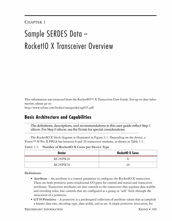
PRELIMINARY INFORMATION XILINX • 109
CHAPTER 1
Sample SERDES Data --
RocketIO X Transceiver Overview
This information was extracted from the RocketIO™ X Transceiver User Guide. For up-to-date infor-mation, please go to: http://www.xilinx.com/bvdocs/userguides/ug035.pdf
Basic Architecture and Capabilities
The definitions, descriptions, and recommendations in this user guide reflect Step 1silicon. For Step 0 silicon, see the Errata for special considerations.
The RocketIO X block diagram is illustrated in Figure 1-1. Depending on the device, a Virtex™-II Pro X FPGA has between 8 and 20 transceiver modules, as shown in Table 1-1.
Definitions:
• Attribute – An attribute is a control parameter to configure the RocketIO X transceiver. There are both primitive ports (traditional I/O ports for control and status) and transceiver attributes. Transceiver attributes are also controls to the transceiver that regulate data widths and encoding rules, but controls that are configured as a group in “soft” form through the invocation of a primitive.
• GT10 Primitive – A primitive is a predesigned collection of attribute values that accomplish a known data rate, encoding type, data width, and so on. A single primitive invocation, for
TABLE 1-1: Number of RocketIO X Cores per Device Type
Device RocketIO X Cores
XC2VPX20 8
XC2VPX70 20
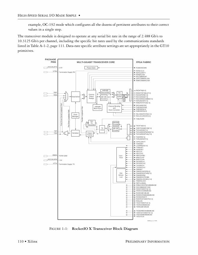
HIGH-SPEED SERIAL I/O MADE SIMPLE •
110 • Xilinx PRELIMINARY INFORMATION
example, OC-192 mode which configures all the dozens of pertinent attributes to their correct values in a single step.
The transceiver module is designed to operate at any serial bit rate in the range of 2.488 Gb/s to 10.3125 Gb/s per channel, including the specific bit rates used by the communications standards listed in Table A-1-2, page 111. Data-rate specific attribute settings are set appropriately in the GT10 primitives.
FIGURE 1-1: RocketIO X Transceiver Block Diagram
FPGA FABRICMULTI-GIGABIT TRANSCEIVER CORE
Serializer
RXP
TXP
ClockManager
Power Down
PACKAGEPINS
DeserializerCommaDetectRealign
8B/10B Decoder
TXFIFO
Channel Bondingand
Clock Correction CHBONDI[4:0]CHBONDO[4:0]
8B/10BEncoder
RXElasticBuffer
OutputPolarity
RXN
GNDA
TXN
UG035_01_111303
POWERDOWN
RXRECCLKRXPOLARITYRXREALIGNRXCOMMADET
RXRESET
RXCLKCORCNT[2:0]RXLOSSOFSYNC[1:0]
RXDATA[63:0]
RXNOTINTABLE[7:0]RXDISPERR[7:0]RXCHARISK[7:0]RXCHARISCOMMA[7:0]RXRUNDISP[7:0]RXBUFSTATUS[1:0]
ENCHANSYNC
RXUSRCLKRXUSRCLK2
CHBONDDONE
TXBUFERR
TXDATA[63:0]
TXBYPASS8B10B[7:0]TXCHARISK[7:0]TXCHARDISPMODE[7:0]TXCHARDISPVAL[7:0]
TXKERR[7:0]TXRUNDISP[7:0]
TXPOLARITYTXINHIBITLOOPBACK[1:0]TXRESET
REFCLKREFCLK2REFCLKSEL
ENPCOMMAALIGNENMCOMMAALIGN
TXUSRCLKTXUSRCLK2
VTRX
AVCCAUXTX
VTTX
AVCCAUXRX
2.5V
TX/RX GND
Termination Supply RX
1.5V
Termination Supply TX
Pos
t Driv
er S
eria
l Loo
pbac
k P
ath
Par
alle
l Loo
pbac
k P
ath
BREFCLKPBREFCLKN
64B/66BBlock Sync
64B
/66B
Dec
oder
Gear Box
Scrambler
64B/66BEncoder
PMAAttribute
Load
PMAREGDATAIN[7:0]
RXCOMMADETUSERXDATAWIDTH[1:0]RXDECC64B66BUSE
PMAINITPMAREGADDR[5:0]
PMAREGRWPMAREGSTROBEPMARXLOCKSEL[1:0]PMARXLOCK
RXDEC8B10BUSERXDESCRAM64B66BUSE
REFCLKBSELRXBLCOKSYNC64B66BUSE
RXSLIDE
TXINTDATAWIDTH[1:0]TXSCRAM64B66BUSETXOUTCLK
RXIGNOREBTFRXINTDATAWIDTH[1:0]
TXDATAWIDTH[1:0]TXENC64B66BUSETXENC8B10BUSE
TXGEARBOX64B66BUSE
Pre
-Driv
er L
oopb
ack
Pat
h
64B/66BDescrambler
Clock / Reset
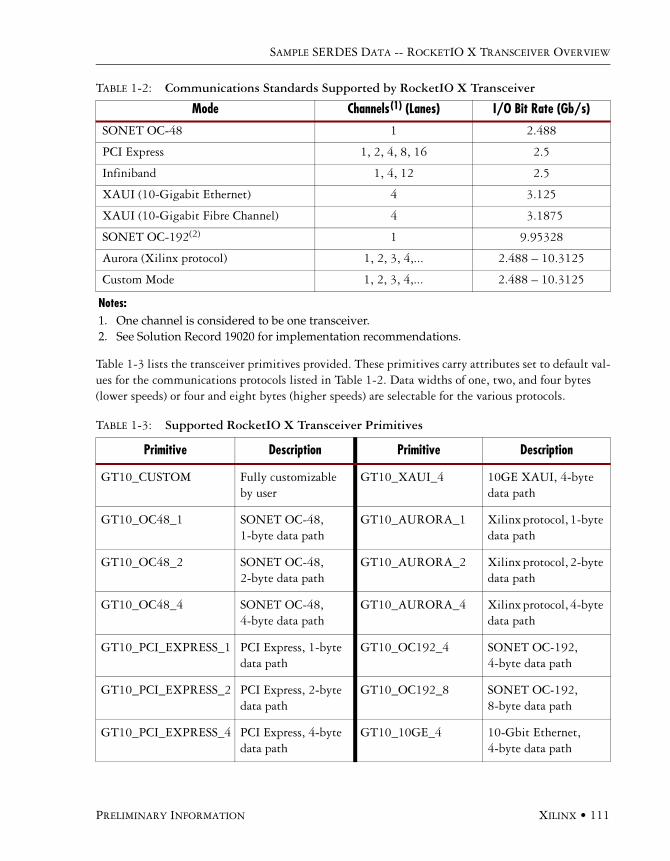
SAMPLE SERDES DATA -- ROCKETIO X TRANSCEIVER OVERVIEW
PRELIMINARY INFORMATION XILINX • 111
.
Table 1-3 lists the transceiver primitives provided. These primitives carry attributes set to default val-ues for the communications protocols listed in Table 1-2. Data widths of one, two, and four bytes (lower speeds) or four and eight bytes (higher speeds) are selectable for the various protocols.
TABLE 1-2: Communications Standards Supported by RocketIO X Transceiver
Mode Channels(1) (Lanes) I/O Bit Rate (Gb/s)
SONET OC-48 1 2.488
PCI Express 1, 2, 4, 8, 16 2.5
Infiniband 1, 4, 12 2.5
XAUI (10-Gigabit Ethernet) 4 3.125
XAUI (10-Gigabit Fibre Channel) 4 3.1875
SONET OC-192(2) 1 9.95328
Aurora (Xilinx protocol) 1, 2, 3, 4,... 2.488 – 10.3125
Custom Mode 1, 2, 3, 4,... 2.488 – 10.3125
Notes: 1. One channel is considered to be one transceiver.2. See Solution Record 19020 for implementation recommendations.
TABLE 1-3: Supported RocketIO X Transceiver Primitives
Primitive Description Primitive Description
GT10_CUSTOM Fully customizable by user
GT10_XAUI_4 10GE XAUI, 4-byte data path
GT10_OC48_1 SONET OC-48, 1-byte data path
GT10_AURORA_1 Xilinx protocol, 1-byte data path
GT10_OC48_2 SONET OC-48, 2-byte data path
GT10_AURORA_2 Xilinx protocol, 2-byte data path
GT10_OC48_4 SONET OC-48, 4-byte data path
GT10_AURORA_4 Xilinx protocol, 4-byte data path
GT10_PCI_EXPRESS_1 PCI Express, 1-byte data path
GT10_OC192_4 SONET OC-192, 4-byte data path
GT10_PCI_EXPRESS_2 PCI Express, 2-byte data path
GT10_OC192_8 SONET OC-192, 8-byte data path
GT10_PCI_EXPRESS_4 PCI Express, 4-byte data path
GT10_10GE_4 10-Gbit Ethernet, 4-byte data path

HIGH-SPEED SERIAL I/O MADE SIMPLE •
112 • Xilinx PRELIMINARY INFORMATION
There are three ways to configure the RocketIO X transceiver:
• Static properties can be set through attributes in the HDL code. Use of attributes are covered in detail in “Primitive Attributes,” page 120.
• Dynamic changes can be made to the attributes via the attribute programming bus. • Dynamic changes can be made through the ports of the primitives.The RocketIO X transceiver consists of the Physical Media Attachment (PMA) and Physical Cod-
ing Sublayer (PCS). The PMA contains the serializer/deserializer (SERDES), TX and RX buffers, clock generator, and clock recovery circuitry. The PCS contains the 8b/10b encoder/decoder, 64b/66b encoder/decoder/scrambler/descrambler, and the elastic buffer supporting channel bonding and clock correction. Refer again to Table 1-1, page 110, showing the RocketIO X transceiver top-level block diagram and FPGA interface signals.
RocketIO X Transceiver InstantiationsFor the different clocking schemes, several things must change, including the clock frequency for USRCLK and USRCLK2. The data and control ports for GT10_CUSTOM always use maximum bus widths. To implement the designs that do not take full advantage of the bus width, concatenate zeros onto inputs and the wires for outputs for Verilog designs, and set outputs to open and concatenate zeros on unused input bits for VHDL designs.
HDL Code ExamplesThe Architecture Wizard can be used to create instantiation templates. This wizard creates code and instantiation templates that define the attributes for a specific application.
GT10_INFINIBAND_1 Infiniband, 1-byte data path
GT10_10GE_8 10-Gbit Ethernet, 8-byte data path
GT10_INFINIBAND_2 Infiniband, 2-byte data path
GT10_10GFC_4 10-Gbit Fibre Channel, 4-byte data path
GT10_INFINIBAND_4 Infiniband, 4-byte data path
GT10_10GFC_8 10-Gbit Fibre Channel, 8-byte data path
GT10_XAUI_1 10GE XAUI, 1-byte data path
GT10_AURORAX_4 Xilinx 10G protocol, 4-byte data path
GT10_XAUI_2 10GE XAUI, 2-byte data path
GT10_AURORAX_8 Xilinx 10G protocol, 8-byte data path
TABLE 1-3: Supported RocketIO X Transceiver Primitives (Continued)
Primitive Description Primitive Description
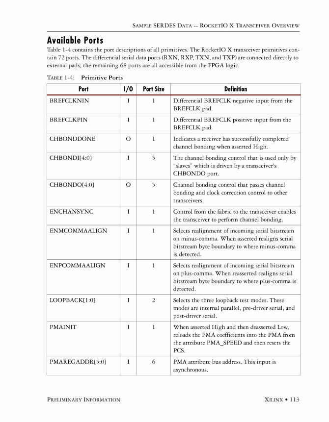
SAMPLE SERDES DATA -- ROCKETIO X TRANSCEIVER OVERVIEW
PRELIMINARY INFORMATION XILINX • 113
Available PortsTable 1-4 contains the port descriptions of all primitives. The RocketIO X transceiver primitives con-tain 72 ports. The differential serial data ports (RXN, RXP, TXN, and TXP) are connected directly to external pads; the remaining 68 ports are all accessible from the FPGA logic.
TABLE 1-4: Primitive Ports
Port I/O Port Size Definition
BREFCLKNIN I 1 Differential BREFCLK negative input from the BREFCLK pad.
BREFCLKPIN I 1 Differential BREFCLK positive input from the BREFCLK pad.
CHBONDDONE O 1 Indicates a receiver has successfully completed channel bonding when asserted High.
CHBONDI[4:0] I 5 The channel bonding control that is used only by “slaves” which is driven by a transceiver's CHBONDO port.
CHBONDO[4:0] O 5 Channel bonding control that passes channel bonding and clock correction control to other transceivers.
ENCHANSYNC I 1 Control from the fabric to the transceiver enables the transceiver to perform channel bonding.
ENMCOMMAALIGN I 1 Selects realignment of incoming serial bitstream on minus-comma. When asserted realigns serial bitstream byte boundary to where minus-comma is detected.
ENPCOMMAALIGN I 1 Selects realignment of incoming serial bitstream on plus-comma. When reasserted realigns serial bitstream byte boundary to where plus-comma is detected.
LOOPBACK[1:0] I 2 Selects the three loopback test modes. These modes are internal parallel, pre-driver serial, and post-driver serial.
PMAINIT I 1 When asserted High and then deasserted Low, reloads the PMA coefficients into the PMA from the attribute PMA_SPEED and then resets the PCS.
PMAREGADDR[5:0] I 6 PMA attribute bus address. This input is asynchronous.

HIGH-SPEED SERIAL I/O MADE SIMPLE •
114 • Xilinx PRELIMINARY INFORMATION
PMAREGDATAIN[7:0] I 8 PMA attribute bus data input. This input is asynchronous.
PMAREGRW I 1 PMA attribute bus read/write control. This input is asynchronous.
PMAREGSTROBE I 1 PMA attribute bus strobe. Note: This input is asynchronous.
PMARXLOCK O 1 Indicates that the receive PLL has locked in the fine loop. When RX PLL is set to “Lock to Data,” this signal is always a logic 1.
PMARXLOCKSEL[1:0] I 2 Selects determination of lock in the receive PLL.
POWERDOWN I 1 Shuts down both the receiver and transmitter sides of the transceiver when asserted High. Note: This input is asynchronous.
REFCLK I 1 The reference clock net that is embedded within the fabric.
REFCLK2 I 1 An alternative to REFCLK. Can be selected by the REFCLKSEL.
REFCLKBSEL I 1 Selects between BREFCLK and REFCLK/REFCLK2 as reference clock. Asserted selects BREFCLK. Deasserted selects REFCLK or REFCLK2, depending on REFCLKSEL.
REFCLKSEL I 1 Selects between REFCLK or REFCLK2 as reference clock. Deasserted selects REFCLK. Asserted selects REFCLK2.
RXBUFSTATUS[1:0] O 2 Receiver elastic buffer status. Indicates the status of the receive FIFO pointers, channel bonding skew, and clock correction events.
RXBLOCKSYNC64B66BUSE
I 1 If asserted, the block sync is used. If deasserted, the block sync logic is bypassed.
RXCHARISCOMMA[7:0]
O 1, 2, 4, 8(1) Indicates the reception of K28.0, K28.5, K28.7, and some out of band commas (depending on the setting of DEC_VALID_COMMA_ONLY by the 8b/10b decoder.
TABLE 1-4: Primitive Ports (Continued)
Port I/O Port Size Definition
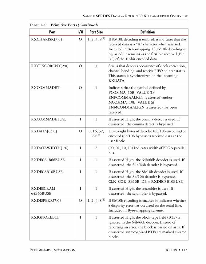
SAMPLE SERDES DATA -- ROCKETIO X TRANSCEIVER OVERVIEW
PRELIMINARY INFORMATION XILINX • 115
RXCHARISK[7:0] O 1, 2, 4, 8(1) If 8b/10b decoding is enabled, it indicates that the received data is a “K” character when asserted. Included in Byte-mapping. If 8b/10b decoding is bypassed, it remains as the first bit received (Bit “a”) of the 10-bit encoded data
RXCLKCORCNT[2:0] O 3 Status that denotes occurrence of clock correction, channel bonding, and receive FIFO pointer status. This status is synchronized on the incoming RXDATA.
RXCOMMADET O 1 Indicates that the symbol defined by PCOMMA_10B_VALUE (IF ENPCOMMAALIGN is asserted) and/or MCOMMA_10B_VALUE (if ENMCOMMAALIGN is asserted) has been received.
RXCOMMADETUSE I 1 If asserted High, the comma detect is used. If deasserted, the comma detect is bypassed.
RXDATA[63:0] O 8, 16, 32, 64(2)
Up to eight bytes of decoded (8b/10b encoding) or encoded (8b/10b bypassed) received data at the user fabric.
RXDATAWIDTH[1:0] I 2 (00, 01, 10, 11) Indicates width of FPGA parallel bus.
RXDEC64B66BUSE I 1 If asserted High, the 64b/66b decoder is used. If deasserted, the 64b/66b decoder is bypassed.
RXDEC8B10BUSE I 1 If asserted High, the 8b/10b decoder is used. If deasserted, the 8b/10b decoder is bypassed. CLK_COR_8B10B_DE = RXDEC8B10BUSE
RXDESCRAM64B66BUSE
I 1 If asserted High, the scrambler is used. If deasserted, the scrambler is bypassed.
RXDISPERR[7:0] O 1, 2, 4, 8(1) If 8b/10b encoding is enabled it indicates whether a disparity error has occurred on the serial line. Included in Byte-mapping scheme.
RXIGNOREBTF I 1 If asserted High, the block type field (BTF) is ignored in the 64b/66b decoder. Instead of reporting an error, the block is passed on as is. If deasserted, unrecognized BTFs are marked as error blocks.
TABLE 1-4: Primitive Ports (Continued)
Port I/O Port Size Definition

HIGH-SPEED SERIAL I/O MADE SIMPLE •
116 • Xilinx PRELIMINARY INFORMATION
RXINTDATAWIDTH[1:0]
I 2 (00, 01, 10, 11) Sets the internal mode of the receive PCS, either 16-, 20-, 32-, or 40-bit.
RXLOSSOFSYNC[1:0] O 2 Bit 0 is always zero. Bit 1 indicates there is a 64b/66b Block Lock when deasserted to logic Low.
RXN I 1 Serial differential port (FPGA external)
RXNOTINTABLE[7:0] O 1, 2, 4, 8(1) Status of encoded data when the data is not a valid character when asserted High. Applies to the byte-mapping scheme.
RXP I 1 Serial differential port (FPGA external)
RXPOLARITY I 1 Similar to TXPOLARITY, but for RXN and RXP. When deasserted, assumes regular polarity. When asserted, reverses polarity.
RXREALIGN O 1 Signal from the PMA denoting that the byte alignment with the serial data stream changed due to a comma detection. Asserted High when alignment occurs.
RXRECCLK O 1 Clock recovered from the data stream and divided. Divide ratio depends on PMA_SPEED setting and/or PMA attributes.
RXRESET I 1 Synchronous RX system reset that “recenters” the receive elastic buffer. It also resets 8b/10b decoder, comma detect, channel bonding, clock correction logic, and other internal receive registers. It does not reset the receiver PLL.
RXRUNDISP[7:0] O 1, 2, 4, 8(1) Signals the running disparity (0 = negative, 1 = positive) in the received serial data. If 8b/10b encoding is bypassed, it remains as the second bit received (Bit “b”) of the 10-bit encoded data.
RXSLIDE I 1 Enables the “slip” of the detection block by 1-bit. To enable a slide of 1-bit, it increments from a lower bit to a higher bit. This signal must be asserted and then deasserted synchronous to RXUSRCKLK2. RXSLIDE must be held Low for at least two clock cycles before being asserted High again.
TABLE 1-4: Primitive Ports (Continued)
Port I/O Port Size Definition
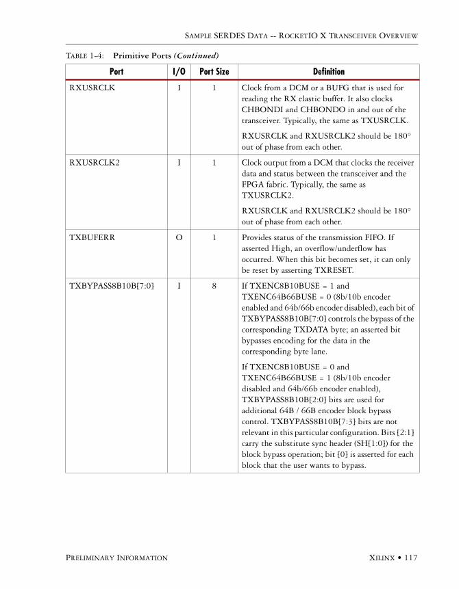
SAMPLE SERDES DATA -- ROCKETIO X TRANSCEIVER OVERVIEW
PRELIMINARY INFORMATION XILINX • 117
RXUSRCLK I 1 Clock from a DCM or a BUFG that is used for reading the RX elastic buffer. It also clocks CHBONDI and CHBONDO in and out of the transceiver. Typically, the same as TXUSRCLK.
RXUSRCLK and RXUSRCLK2 should be 180° out of phase from each other.
RXUSRCLK2 I 1 Clock output from a DCM that clocks the receiver data and status between the transceiver and the FPGA fabric. Typically, the same as TXUSRCLK2.
RXUSRCLK and RXUSRCLK2 should be 180° out of phase from each other.
TXBUFERR O 1 Provides status of the transmission FIFO. If asserted High, an overflow/underflow has occurred. When this bit becomes set, it can only be reset by asserting TXRESET.
TXBYPASS8B10B[7:0] I 8 If TXENC8B10BUSE = 1 and TXENC64B66BUSE = 0 (8b/10b encoder enabled and 64b/66b encoder disabled), each bit of TXBYPASS8B10B[7:0] controls the bypass of the corresponding TXDATA byte; an asserted bit bypasses encoding for the data in the corresponding byte lane.
If TXENC8B10BUSE = 0 and TXENC64B66BUSE = 1 (8b/10b encoder disabled and 64b/66b encoder enabled), TXBYPASS8B10B[2:0] bits are used for additional 64B / 66B encoder block bypass control. TXBYPASS8B10B[7:3] bits are not relevant in this particular configuration. Bits [2:1] carry the substitute sync header (SH[1:0]) for the block bypass operation; bit [0] is asserted for each block that the user wants to bypass.
TABLE 1-4: Primitive Ports (Continued)
Port I/O Port Size Definition
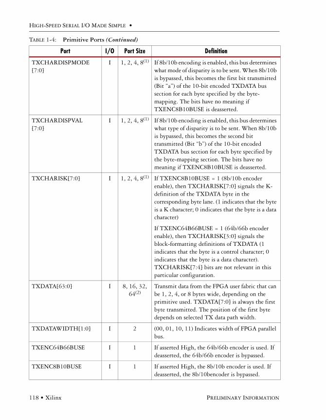
HIGH-SPEED SERIAL I/O MADE SIMPLE •
118 • Xilinx PRELIMINARY INFORMATION
TXCHARDISPMODE[7:0]
I 1, 2, 4, 8(1) If 8b/10b encoding is enabled, this bus determines what mode of disparity is to be sent. When 8b/10b is bypassed, this becomes the first bit transmitted (Bit “a”) of the 10-bit encoded TXDATA bus section for each byte specified by the byte-mapping. The bits have no meaning if TXENC8B10BUSE is deasserted.
TXCHARDISPVAL[7:0]
I 1, 2, 4, 8(1) If 8b/10b encoding is enabled, this bus determines what type of disparity is to be sent. When 8b/10b is bypassed, this becomes the second bit transmitted (Bit “b”) of the 10-bit encoded TXDATA bus section for each byte specified by the byte-mapping section. The bits have no meaning if TXENC8B10BUSE is deasserted.
TXCHARISK[7:0] I 1, 2, 4, 8(1) If TXENC8B10BUSE = 1 (8b/10b encoder enable), then TXCHARISK[7:0] signals the K-definition of the TXDATA byte in the corresponding byte lane. (1 indicates that the byte is a K character; 0 indicates that the byte is a data character)
If TXENC64B66BUSE = 1 (64b/66b encoder enable), then TXCHARISK[3:0] signals the block-formatting definitions of TXDATA (1 indicates that the byte is a control character; 0 indicates that the byte is a data character). TXCHARISK[7:4] bits are not relevant in this particular configuration.
TXDATA[63:0] I 8, 16, 32, 64(2)
Transmit data from the FPGA user fabric that can be 1, 2, 4, or 8 bytes wide, depending on the primitive used. TXDATA[7:0] is always the first byte transmitted. The position of the first byte depends on selected TX data path width.
TXDATAWIDTH[1:0] I 2 (00, 01, 10, 11) Indicates width of FPGA parallel bus.
TXENC64B66BUSE I 1 If asserted High, the 64b/66b encoder is used. If deasserted, the 64b/66b encoder is bypassed.
TXENC8B10BUSE I 1 If asserted High, the 8b/10b encoder is used. If deasserted, the 8b/10bencoder is bypassed.
TABLE 1-4: Primitive Ports (Continued)
Port I/O Port Size Definition
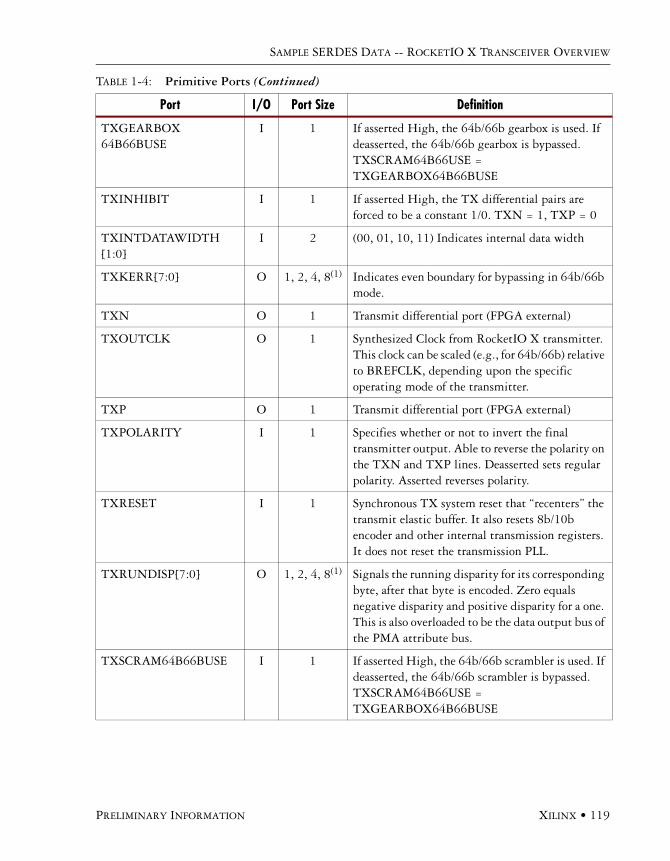
SAMPLE SERDES DATA -- ROCKETIO X TRANSCEIVER OVERVIEW
PRELIMINARY INFORMATION XILINX • 119
TXGEARBOX64B66BUSE
I 1 If asserted High, the 64b/66b gearbox is used. If deasserted, the 64b/66b gearbox is bypassed. TXSCRAM64B66USE = TXGEARBOX64B66BUSE
TXINHIBIT I 1 If asserted High, the TX differential pairs are forced to be a constant 1/0. TXN = 1, TXP = 0
TXINTDATAWIDTH[1:0]
I 2 (00, 01, 10, 11) Indicates internal data width
TXKERR[7:0] O 1, 2, 4, 8(1) Indicates even boundary for bypassing in 64b/66b mode.
TXN O 1 Transmit differential port (FPGA external)
TXOUTCLK O 1 Synthesized Clock from RocketIO X transmitter. This clock can be scaled (e.g., for 64b/66b) relative to BREFCLK, depending upon the specific operating mode of the transmitter.
TXP O 1 Transmit differential port (FPGA external)
TXPOLARITY I 1 Specifies whether or not to invert the final transmitter output. Able to reverse the polarity on the TXN and TXP lines. Deasserted sets regular polarity. Asserted reverses polarity.
TXRESET I 1 Synchronous TX system reset that “recenters” the transmit elastic buffer. It also resets 8b/10b encoder and other internal transmission registers. It does not reset the transmission PLL.
TXRUNDISP[7:0] O 1, 2, 4, 8(1) Signals the running disparity for its corresponding byte, after that byte is encoded. Zero equals negative disparity and positive disparity for a one. This is also overloaded to be the data output bus of the PMA attribute bus.
TXSCRAM64B66BUSE I 1 If asserted High, the 64b/66b scrambler is used. If deasserted, the 64b/66b scrambler is bypassed. TXSCRAM64B66USE = TXGEARBOX64B66BUSE
TABLE 1-4: Primitive Ports (Continued)
Port I/O Port Size Definition
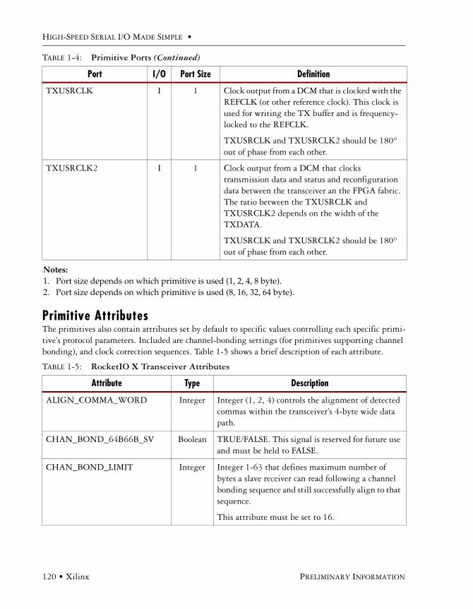
HIGH-SPEED SERIAL I/O MADE SIMPLE •
120 • Xilinx PRELIMINARY INFORMATION
Primitive Attributes The primitives also contain attributes set by default to specific values controlling each specific primi-tive’s protocol parameters. Included are channel-bonding settings (for primitives supporting channel bonding), and clock correction sequences. Table 1-5 shows a brief description of each attribute.
TXUSRCLK I 1 Clock output from a DCM that is clocked with the REFCLK (or other reference clock). This clock is used for writing the TX buffer and is frequency-locked to the REFCLK.
TXUSRCLK and TXUSRCLK2 should be 180° out of phase from each other.
TXUSRCLK2 I 1 Clock output from a DCM that clocks transmission data and status and reconfiguration data between the transceiver an the FPGA fabric. The ratio between the TXUSRCLK and TXUSRCLK2 depends on the width of the TXDATA.
TXUSRCLK and TXUSRCLK2 should be 180° out of phase from each other.
Notes: 1. Port size depends on which primitive is used (1, 2, 4, 8 byte).2. Port size depends on which primitive is used (8, 16, 32, 64 byte).
TABLE 1-5: RocketIO X Transceiver Attributes
Attribute Type Description
ALIGN_COMMA_WORD Integer Integer (1, 2, 4) controls the alignment of detected commas within the transceiver’s 4-byte wide data path.
CHAN_BOND_64B66B_SV Boolean TRUE/FALSE. This signal is reserved for future use and must be held to FALSE.
CHAN_BOND_LIMIT Integer Integer 1-63 that defines maximum number of bytes a slave receiver can read following a channel bonding sequence and still successfully align to that sequence.
This attribute must be set to 16.
TABLE 1-4: Primitive Ports (Continued)
Port I/O Port Size Definition
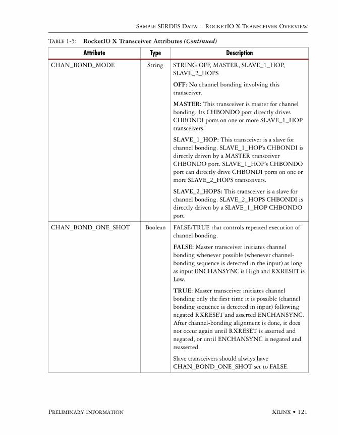
SAMPLE SERDES DATA -- ROCKETIO X TRANSCEIVER OVERVIEW
PRELIMINARY INFORMATION XILINX • 121
CHAN_BOND_MODE String STRING OFF, MASTER, SLAVE_1_HOP, SLAVE_2_HOPS
OFF: No channel bonding involving this transceiver.
MASTER: This transceiver is master for channel bonding. Its CHBONDO port directly drives CHBONDI ports on one or more SLAVE_1_HOP transceivers.
SLAVE_1_HOP: This transceiver is a slave for channel bonding. SLAVE_1_HOP’s CHBONDI is directly driven by a MASTER transceiver CHBONDO port. SLAVE_1_HOP’s CHBONDO port can directly drive CHBONDI ports on one or more SLAVE_2_HOPS transceivers.
SLAVE_2_HOPS: This transceiver is a slave for channel bonding. SLAVE_2_HOPS CHBONDI is directly driven by a SLAVE_1_HOP CHBONDO port.
CHAN_BOND_ONE_SHOT Boolean FALSE/TRUE that controls repeated execution of channel bonding.
FALSE: Master transceiver initiates channel bonding whenever possible (whenever channel-bonding sequence is detected in the input) as long as input ENCHANSYNC is High and RXRESET is Low.
TRUE: Master transceiver initiates channel bonding only the first time it is possible (channel bonding sequence is detected in input) following negated RXRESET and asserted ENCHANSYNC. After channel-bonding alignment is done, it does not occur again until RXRESET is asserted and negated, or until ENCHANSYNC is negated and reasserted.
Slave transceivers should always have CHAN_BOND_ONE_SHOT set to FALSE.
TABLE 1-5: RocketIO X Transceiver Attributes (Continued)
Attribute Type Description

HIGH-SPEED SERIAL I/O MADE SIMPLE •
122 • Xilinx PRELIMINARY INFORMATION
CHAN_BOND_SEQ_1_*[10:0]
11-bit vector
These define the channel bonding sequence. The usage of these vectors also depends on CHAN_BOND_SEQ_LEN and CHAN_BOND_SEQ_2_USE.
CHAN_BOND_SEQ_1_MASK[3:0]
4-bit vector
Each bit of the mask determines if that particular sequence is detected regardless of its value. If bit 0 is High, then CHAN_BOND_SEQ_1_1 is matched regardless of its value.
CHAN_BOND_SEQ_2_*[10:0]
11-bit vector
These define the channel bonding sequence: The usage of these vectors also depends on CHAN_BOND_SEQ_LEN and CHAN_BOND_SEQ_2_USE.
CHAN_BOND_SEQ_2_MASK[3:0]
4-bit vector
Each bit of the mask determines if that particular sequence is detected regardless of its value. If bit 0 is High, then CHAN_BOND_SEQ_2_1 is matched regardless of its value.
CHAN_BOND_SEQ_2_USE Boolean FALSE/TRUE that controls use of second channel bonding sequence.
FALSE: Channel bonding uses only one channel bonding sequence defined by CHAN_BOND_SEQ_1_1 ... 4, or one 8-byte sequence defined by CHAN_BOND_SEQ_1_X and CHAN_BOND_SEQ_2_X in combination.
TRUE: Channel bonding uses two channel bonding sequences defined by CHAN_BOND_SEQ_1_1 ... 4 and CHAN_BOND_SEQ_2_1 ... 4, as further constrained by CHAN_BOND_SEQ_LEN.
CHAN_BOND_SEQ_LEN Integer Integer (1, 2, 3, 4, 8) defines length in bytes of channel bonding sequence. This defines the length of the sequence the transceiver matches to detect opportunities for channel bonding.
CLK_COR_8B10B_DE Boolean This signal selects if clock correction occurs relative to the encoded or decoded version of the 8b/10b stream. If set to TRUE, the decoded version is used. If set to FALSE, the encoded version is used. Must be set in conjunction with RXDEC8B10USE.CLK_COR_8B10B_DE = RXDEC8B10BUSE
TABLE 1-5: RocketIO X Transceiver Attributes (Continued)
Attribute Type Description
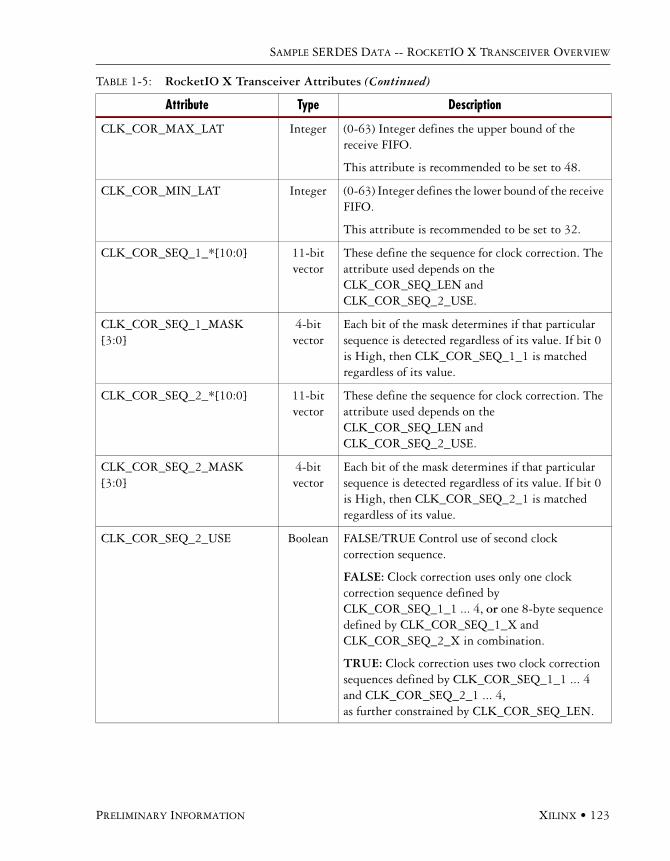
SAMPLE SERDES DATA -- ROCKETIO X TRANSCEIVER OVERVIEW
PRELIMINARY INFORMATION XILINX • 123
CLK_COR_MAX_LAT Integer (0-63) Integer defines the upper bound of the receive FIFO.
This attribute is recommended to be set to 48.
CLK_COR_MIN_LAT Integer (0-63) Integer defines the lower bound of the receive FIFO.
This attribute is recommended to be set to 32.
CLK_COR_SEQ_1_*[10:0] 11-bit vector
These define the sequence for clock correction. The attribute used depends on the CLK_COR_SEQ_LEN and CLK_COR_SEQ_2_USE.
CLK_COR_SEQ_1_MASK[3:0]
4-bit vector
Each bit of the mask determines if that particular sequence is detected regardless of its value. If bit 0 is High, then CLK_COR_SEQ_1_1 is matched regardless of its value.
CLK_COR_SEQ_2_*[10:0] 11-bit vector
These define the sequence for clock correction. The attribute used depends on the CLK_COR_SEQ_LEN and CLK_COR_SEQ_2_USE.
CLK_COR_SEQ_2_MASK[3:0]
4-bit vector
Each bit of the mask determines if that particular sequence is detected regardless of its value. If bit 0 is High, then CLK_COR_SEQ_2_1 is matched regardless of its value.
CLK_COR_SEQ_2_USE Boolean FALSE/TRUE Control use of second clock correction sequence.
FALSE: Clock correction uses only one clock correction sequence defined by CLK_COR_SEQ_1_1 ... 4, or one 8-byte sequence defined by CLK_COR_SEQ_1_X and CLK_COR_SEQ_2_X in combination.
TRUE: Clock correction uses two clock correction sequences defined by CLK_COR_SEQ_1_1 ... 4 and CLK_COR_SEQ_2_1 ... 4, as further constrained by CLK_COR_SEQ_LEN.
TABLE 1-5: RocketIO X Transceiver Attributes (Continued)
Attribute Type Description
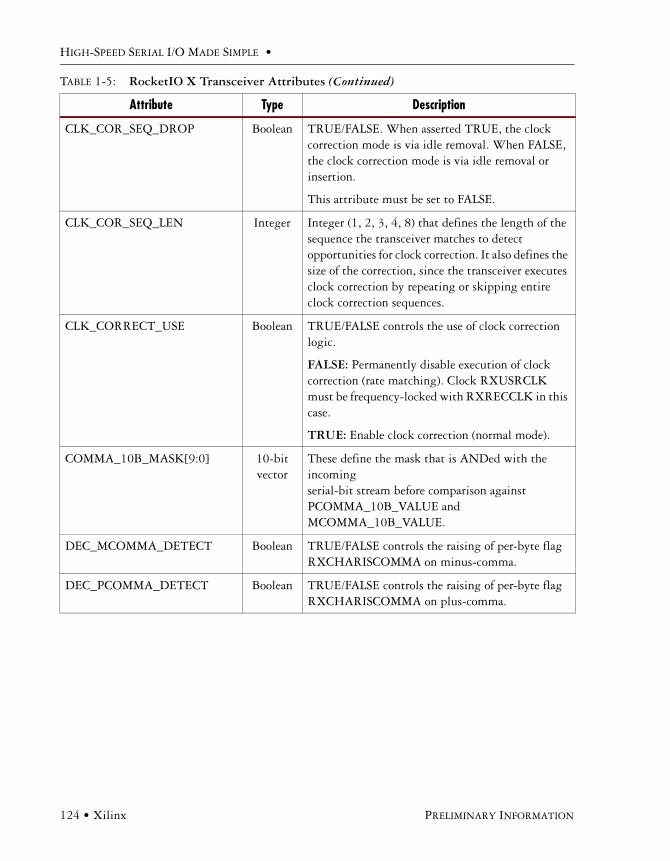
HIGH-SPEED SERIAL I/O MADE SIMPLE •
124 • Xilinx PRELIMINARY INFORMATION
CLK_COR_SEQ_DROP Boolean TRUE/FALSE. When asserted TRUE, the clock correction mode is via idle removal. When FALSE, the clock correction mode is via idle removal or insertion.
This attribute must be set to FALSE.
CLK_COR_SEQ_LEN Integer Integer (1, 2, 3, 4, 8) that defines the length of the sequence the transceiver matches to detect opportunities for clock correction. It also defines the size of the correction, since the transceiver executes clock correction by repeating or skipping entire clock correction sequences.
CLK_CORRECT_USE Boolean TRUE/FALSE controls the use of clock correction logic.
FALSE: Permanently disable execution of clock correction (rate matching). Clock RXUSRCLK must be frequency-locked with RXRECCLK in this case.
TRUE: Enable clock correction (normal mode).
COMMA_10B_MASK[9:0] 10-bit vector
These define the mask that is ANDed with the incoming serial-bit stream before comparison against PCOMMA_10B_VALUE and MCOMMA_10B_VALUE.
DEC_MCOMMA_DETECT Boolean TRUE/FALSE controls the raising of per-byte flag RXCHARISCOMMA on minus-comma.
DEC_PCOMMA_DETECT Boolean TRUE/FALSE controls the raising of per-byte flag RXCHARISCOMMA on plus-comma.
TABLE 1-5: RocketIO X Transceiver Attributes (Continued)
Attribute Type Description

SAMPLE SERDES DATA -- ROCKETIO X TRANSCEIVER OVERVIEW
PRELIMINARY INFORMATION XILINX • 125
DEC_VALID_COMMA_ONLY
Boolean TRUE/FALSE controls the raising of RXCHARISCOMMA on an invalid comma.
FALSE: Raise RXCHARISCOMMA on:
xxx1111100 (if DEC_PCOMMA_DETECT is TRUE)
and/or on:
xxx0000011 (if DEC_MCOMMA_DETECT is TRUE)
or on 8b/10b translation commas
regardless of the settings of the xxx bits.
TRUE: Raise RXCHARISCOMMA only on valid characters that are in the 8b/10b translation.
MCOMMA_10B_VALUE[9:0]
10-bit vector
These define minus-comma for the purpose of raising RXCOMMADET and realigning the serial bit stream byte boundary. This definition does not affect 8b/10b encoding or decoding. Also see COMMA_10B_MASK.
MCOMMA_DETECT Boolean TRUE/FALSE indicates whether to raise or not raise the RXCOMMADET when minus-comma is detected.
PCOMMA_10B_VALUE[9:0] 10-bit vector
These define plus-comma for the purpose of raising RXCOMMADET and realigning the serial bit stream byte boundary. This definition does not affect 8b/10b encoding or decoding. Also see COMMA_10B_MASK.
PCOMMA_DETECT Boolean TRUE/FALSE indicates whether to raise or not raise the RXCOMMADET when plus-comma is detected.
PMA_PWR _CNTRL Integer This masks the startup sequence of the PMA and must always be set to all ones.
PMA_SPEED String (13_40) Selects the mode of the PMA. Refer to PMA section for the proper mode selection.
RX_BUFFER_USE Boolean TRUE/FALSE. Recommended to always be set to TRUE. Enables the use of the receive side buffer. When set to TRUE, the buffer is enabled.
TABLE 1-5: RocketIO X Transceiver Attributes (Continued)
Attribute Type Description

HIGH-SPEED SERIAL I/O MADE SIMPLE •
126 • Xilinx PRELIMINARY INFORMATION
Modifiable Attributes As shown in Appendix F, “Modifiable Attributes” of the RocketIO X User Guide only certain attributes are modifiable for any primitive. These attributes help to define the protocol used by the primitive. Only the GT10_CUSTOM primitive allows the user to modify all of the attributes to a pro-tocol not supported by another transceiver primitive. This allows for complete flexibility. The other primitives allow modification of the analog attributes of the serial data lines and several channel-bond-ing values.
Byte MappingMost of the 8-bit wide status and control buses correlate to a specific byte of the TXDATA or RXDATA. This scheme is shown in Table 1-6. This creates a way to tie all the signals together regard-less of the data path width needed for the GT10_CUSTOM. All other primitives with specific data width paths and all byte-mapped ports are affected by this situation. For example, a 1-byte wide data
RX_LOS_INVALID_INCR[7:0] Integer Power of two in a range of 1 to 128 that denotes the number of valid characters required to "cancel out" appearance of one invalid character for loss of sync determination.
RX_LOS_THRESHOLD Integer Power of two in a range of 4 to 512. When divided by RX_LOS_INVALID_INCR, denotes the number of invalid characters required to cause FSM transition to “sync lost” state.
RX_LOSS_OF_SYNC_FSM Boolean Undefined.
SH_CNT_MAX[7:0] 8-bit vector
8-bit binary; controls when the 64b/66b synchronization state machine enters synchronization. (max sync header count)
SH_INVALID_CNT_MAX[7:0]
8-bit vector
8-bit binary; controls when the 64b/66b synchronization state machine leaves synchronization. (max invalid sync header count)
TX_BUFFER_USE Boolean When set to TRUE, this enables the use of the transmit buffer.
TABLE 1-5: RocketIO X Transceiver Attributes (Continued)
Attribute Type Description
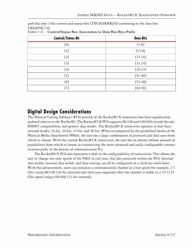
SAMPLE SERDES DATA -- ROCKETIO X TRANSCEIVER OVERVIEW
PRELIMINARY INFORMATION XILINX • 127
path has only 1-bit control and status bits (TXCHARISK[0]) correlating to the data bits TXDATA[7:0].
Digital Design ConsiderationsThe Physical Coding Sublayer (PCS) portion of the RocketIO X transceiver has been significantly updated relative to the RocketIO. The RocketIO X PCS supports 8b/10b and 64b/66b encode/decode, SONET compatibility, and generic data modes. The RocketIO X transceiver operates in four basic internal modes: 16-bit, 20-bit, 32-bit, and 40-bit. When accompanied by the predefined modes of the Physical Media Attachment (PMA), the user has a large combination of protocols and data rates from which to choose. With the custom RocketIO X transceiver, the user has an almost infinite amount of possibilities from which to choose in constructing the most advanced and easily configurable commu-nication paths in the history of communication ICs.
The RocketIO X PCS also represents a shift in the configurability of transceivers. This allows the user to change not only speeds of the PMA in real time, but also protocols within the PCS. Internal data width, external data width, and data routing can all be configured on a clock-by-clock basis. With this advancement, users can initialize a communication channel at a low speed (for example, 2.5 Gb/s using 8b/10b (20-bit internal) and then auto-negotiate after the channel is stable to a 10.3125 Gb/s speed using 64b/66b (32-bit internal).
TABLE 1-6: Control/Status Bus Association to Data Bus Byte Paths
Control/Status Bit Data Bits
[0] [7:0]
[1] [15:8]
[2] [23:16]
[3] [31:24]
[4] [39:32]
[5] [47:40]
[6] [55:48]
[7] [64:56]

HIGH-SPEED SERIAL I/O MADE SIMPLE •
128 • Xilinx PRELIMINARY INFORMATION
The information in this section is provided to RocketIO X users as a reference forunderstanding the individual attribute and control port settings within a primitive. Usershave the choice of using the supported primitives in Table A-1-3, page 111, and ignoring thischapter, or using this chapter to better understand PCS configuration and/or to modifyattribute and port values to create a user transceiver configuration.
Top-Level Architecture
Transmit ArchitectureThe transmit architecture for the PCS is shown in Figure 1-2. For information about bypassing partic-ular blocks, consult the block function section for that particular block.
FIGURE 1-2: Transmit Architecture
6x40 bitTXFIFO 8B/10B
Encode
Gearbox
10G Encode
TXUSRCLK
TXUSRCLK2
TXENC8B10BUSETXENC6466USE
TXSCRAM64B66BUSETXGEARBOX64B66BUSE
TXPOLARITY
PMA
Scrambler
PMAConvert
TX_BUFFER_USEResetControl
PMAAttribute
Load
Fabric C
onvert
PM
AIN
IT
UG035_CH3_01_092903
TXDATA
TXRESET
TXP
TXN

SAMPLE SERDES DATA -- ROCKETIO X TRANSCEIVER OVERVIEW
PRELIMINARY INFORMATION XILINX • 129
Receive ArchitectureThe receive architecture for the PCS is shown in Figure 1-3. For information about bypassing partic-ular blocks, consult the block function section for that particular block.
Operation ModesInternally, there are four modes of operation within the PCS: 16-bit, 20-bit, 32-bit, and 40-bit.
The PCS fundamentally operates in either 2-byte mode, or 4-byte mode, with 2-byte mode cor-responding to 16- and 20-bit mode, and with 4-byte mode corresponding to 32- and 40-bit mode. When in 2-byte mode, the external interface can either be one, two, or four bytes wide. When in 4-byte mode, the external interface can either be 4 or 8 bytes wide. It is not possible to have an internal 2-byte width and an 8-byte external interface. It is also not possible to have an internal 4-byte inter-face, along with a 1-byte external interface. See Table 1-7.
A general guide to use is that 2-byte mode should be used in the PCS when the serial speed is below 5 Gb/s, and the 4-byte mode should be used when the serial speed is greater than 5 Gb/s. In2-byte mode, the PCS processes 4-byte data every other byte. This is transparent to the user, but skews between transceivers result in larger bit skews at the transmit interface as compared to Virtex-II Pro transceivers. Any one of the three encoding schemes (8b/10b and 64b/66b encode/decode, SONET,
FIGURE 1-3: Receive Architecture
TABLE 1-7: PCS Interface Choice
Speed 2 Byte (internal mode) 4 Byte (internal mode)
2.488 Gb/s Recommended Do not use
5 - 10.3125 Gb/s Do not use Recommended
RXCLK0
PMA/PCS Boundary
RX ElasticBuffer16x52
Channel Bonding & ClockCorrection
Fabric
8B/10BDecode
Comma DetectAlign
10GBlockSync
10GDecode
10GDescr
RXRECCLKRXUSRCLK
RXUSRCLK2
Sync State Machine
RXBLOCKSYNCUSE,RXVALUEDETUSE
RXDEC8B10BUSE,RXDESCRAM64B66BUSE RX_BUFFER_USE
RXDEC6466USE
SLIP
Reset Control
HOLDOFF
UG035_CH3_02_092903
EN
PC
OM
MA
ALIG
N
EN
MC
OM
MA
ALIG
N
RX
PO
LAR
ITY
LOC
K
CH
BO
ND
RX
Dat
a W
ord
Alig
nmen
t Mux
RXDATA
RX
RE
SE
T

HIGH-SPEED SERIAL I/O MADE SIMPLE •
130 • Xilinx PRELIMINARY INFORMATION
and generic data modes) can be used in either 2- or 4-byte mode, with each block having a bypass abil-ity.
For more information on setting the PCS mode, refer to the block functional definition of the bus interface in this guide.
Block Level Functions
Classification of Signals and OverloadingThis section describes the pertinent signals at the interface of the PCS and how to prioritize them. For more information about a particular signal, refer to the I/O specification, or the particular block func-tion of interest.
Static Signals (Control Inputs)The following static signals are inputs that control the internal and external mode of operation in the PCS. Typically, these signals would be the first consideration after the mode of operation has been selected:
• RXDATAWIDTH[1:0]• RXINTDATAWIDTH[1:0]• TXDATAWIDTH[1:0]• TXINTDATAWIDTH[1:0]The following static signals are inputs that control the PCS interblock routing and bypass for par-
ticular blocks, which adjust the architecture of the PCS for the user’s particular application:• RXBLOCKSYNC64B66BUSE• RXDEC64B66BUSE• RXDEC8B10BUSE• RXDESCRAM64B66BUSE• RXCOMMADETUSE• TXENC64B66BUSE• TXENC8B10BUSE• TXGEARBOX64B66BUSE• TXSCRAM64B66BUSEThe following static signals are inputs that control various functions, but are usually set once at
the beginning of a state machine, or after an auto-negotiation sequence. They are typically not altered on a clock-by-clock basis:
• ALIGN_COMMA_WORD• ENMCOMMAALIGN• ENPCOMMAALIGN• RXPOLARITY• TXPOLARITY• PMAINIT• RXIGNOREBTF• PMARXLOCKSEL[1:0]The following static signals are inputs that cause either major functional resets or are used in trou-
bleshooting. These signals are mostly used at initialization, not during the functional operation of the circuit:
• LOOPBACK[1:0] (Note: This signal can also be a dynamic signal.)

SAMPLE SERDES DATA -- ROCKETIO X TRANSCEIVER OVERVIEW
PRELIMINARY INFORMATION XILINX • 131
• POWERDOWN• RXRESET• TXRESET• TXINHIBIT
Dynamic SignalsThe following dynamic signals indicate data received on the receive bus, along with status signals that indicate specific information about RXDATA. The set values of these signals define the application setup by the user and are the most important after the static signals are allocated:
• MCOMMA_10B_VALUE• PCOMMA_10B_VALUE• COMMA_10B_MASK• RXCHARISCOMMA[7:0]• RXCHARISK[7:0]• RXDISPERR[7:0]• RXNOTINTABLE[7:0]• RXDATA[63:0]The following dynamic signals indicate data to be transmitted on the transmit bus, along with
status signals that indicate specific information about how TXDATA is to be handled while passing through the PCS. The set values of these signals define the application setup by the user and are the most important after the static signals are allocated:
• TXBYPASS8B10B[7:0]• TXCHARDISPMODE[7:0]• TXCHARDISPVAL[7:0]• TXCHARISK[7:0]• TXDATA[63:0]
The following dynamic signals indicate various status information about the current state or prior state of the PCS:
• CHBONDDONE, RXBUFSTATUS[1:0], RXCLKCORCNT[2:0]• CHBONDO[4:0]• PMARXLOCK• RXLOSSOFSYNC[1:0]• RXREALIGN• RXCOMMADET• TXBUFERR• TXKERR[7:0]• TXRUNDISP[7:0]• RXRUNDISP[7:0]
The following dynamic signals control internal states of the PCS:
• RXSLIDE• CHBONDI[4:0]
The following dynamic signals affect the control registers of the PMA:
• PMAREGADDR[5:0]• PMAREGDATAIN[7:0]

HIGH-SPEED SERIAL I/O MADE SIMPLE •
132 • Xilinx PRELIMINARY INFORMATION
• PMAREGRW• PMAREGSTROBE
Bus InterfaceSelecting the External Configuration (Fabric Interface)By using the signals TXDATAWIDTH[1:0] and RXDATAWIDTH[1:0], the fabric interface can be determined.
Selecting the Internal Configuration
Clock RatioUSRCLK2 clocks the data buffers. The ability to send parallel data to the transceiver at four different widths requires the user to change the frequency of USRCLK2. This creates a frequency ratio between USRCLK and USRCLK2. The falling edges of the clocks must align. See Table 1-10.
TABLE 1-8: Selecting the External Configuration
RXDATAWIDTH/TXDATAWIDTH Data Width Internal Bus Requirements
2’b00 8/10-bit (1 byte) 16-, 20-bit mode
2’b01 16/20-bit (2 byte) 16-, 20-bit mode
2’b10 32/40-bit (4 byte) 16-, 20-, 32-, 40- bit mode
2’b11 64/80-bit (8 byte) 32-, 40-bit mode
TABLE 1-9: Selecting the Internal Configuration
RXINTDATAWIDTH/TXINTDATAWIDTH Internal Data Width
2’b00 16-bit
2’b01 20-bit
2’b10 32-bit
2’b11 40-bit
TABLE 1-10: Data Width Clock Ratios
Fabric Data WidthFrequency Ratio of USRCLK\USRCLK2
2-Byte Internal Data Width 4-Byte Internal Data Width
1 byte 1:2(1) N/A
2 byte 1:1 N/A
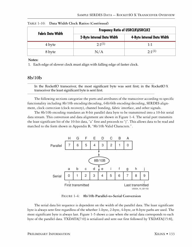
SAMPLE SERDES DATA -- ROCKETIO X TRANSCEIVER OVERVIEW
PRELIMINARY INFORMATION XILINX • 133
8b/10b
In the RocketIO transceiver, the most significant byte was sent first; in the RocketIO Xtransceiver the least significant byte is sent first.
The following sections categorize the ports and attributes of the transceiver according to specific functionality including 8b/10b encoding/decoding, 64b/66b encoding/decoding, SERDES align-ment, clock correction (clock recovery), channel bonding, fabric interface, and other signals.
The 8b/10b encoding translates an 8-bit parallel data byte to be transmitted into a 10-bit serial data stream. This conversion and data alignment are shown in Figure 1-4. The serial port transmits the least significant bit of the 10-bit data, “a” first and proceeds to “j”. This allows data to be read and matched to the form shown in Appendix B, “8b/10b Valid Characters.” .
The serial data bit sequence is dependent on the width of the parallel data. The least significant byte is always sent first regardless of the whether 1-byte, 2-byte, 4-byte, or 8-byte paths are used. The most significant byte is always last. Figure 1-5 shows a case when the serial data corresponds to each byte of the parallel data. TXDATA[7:0] is serialized and sent out first followed by TXDATA[15:8],
4 byte 2:1(1) 1:1
8 byte N/A 2:1(1)
Notes: 1. Each edge of slower clock must align with falling edge of faster clock.
FIGURE 1-4: 8b/10b Parallel-to-Serial Conversion
TABLE 1-10: Data Width Clock Ratios (Continued)
Fabric Data WidthFrequency Ratio of USRCLK\USRCLK2
2-Byte Internal Data Width 4-Byte Internal Data Width
UG024_10_021102
0123457 6
ABCDEFH G
Parallel
7 8 9654320 1
g h jfiedca b
Serial
8B/10B
First transmitted Last transmitted
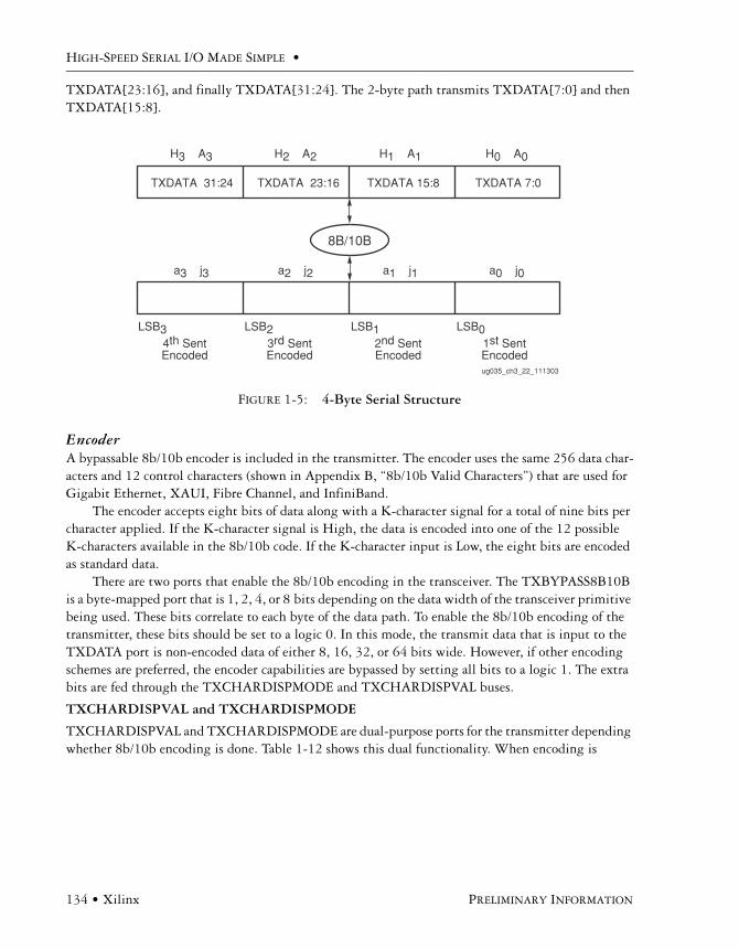
HIGH-SPEED SERIAL I/O MADE SIMPLE •
134 • Xilinx PRELIMINARY INFORMATION
TXDATA[23:16], and finally TXDATA[31:24]. The 2-byte path transmits TXDATA[7:0] and then TXDATA[15:8].
EncoderA bypassable 8b/10b encoder is included in the transmitter. The encoder uses the same 256 data char-acters and 12 control characters (shown in Appendix B, “8b/10b Valid Characters”) that are used for Gigabit Ethernet, XAUI, Fibre Channel, and InfiniBand.
The encoder accepts eight bits of data along with a K-character signal for a total of nine bits per character applied. If the K-character signal is High, the data is encoded into one of the 12 possible K-characters available in the 8b/10b code. If the K-character input is Low, the eight bits are encoded as standard data.
There are two ports that enable the 8b/10b encoding in the transceiver. The TXBYPASS8B10B is a byte-mapped port that is 1, 2, 4, or 8 bits depending on the data width of the transceiver primitive being used. These bits correlate to each byte of the data path. To enable the 8b/10b encoding of the transmitter, these bits should be set to a logic 0. In this mode, the transmit data that is input to the TXDATA port is non-encoded data of either 8, 16, 32, or 64 bits wide. However, if other encoding schemes are preferred, the encoder capabilities are bypassed by setting all bits to a logic 1. The extra bits are fed through the TXCHARDISPMODE and TXCHARDISPVAL buses.
TXCHARDISPVAL and TXCHARDISPMODE
TXCHARDISPVAL and TXCHARDISPMODE are dual-purpose ports for the transmitter depending whether 8b/10b encoding is done. Table 1-12 shows this dual functionality. When encoding is
FIGURE 1-5: 4-Byte Serial Structure
ug035_ch3_22_111303
TXDATA 31:24 TXDATA 23:16 TXDATA 15:8 TXDATA 7:0
H3 A3 H2 A2 H1 A1 H0 A0
a3 j3 a2 j2 a1 j1 a0 j0
8B/10B
LSB3 LSB2 LSB1 LSB01st SentEncoded
2nd SentEncoded
3rd SentEncoded
4th SentEncoded
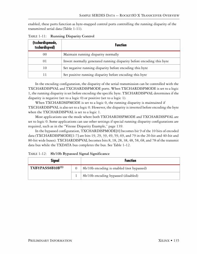
SAMPLE SERDES DATA -- ROCKETIO X TRANSCEIVER OVERVIEW
PRELIMINARY INFORMATION XILINX • 135
enabled, these ports function as byte-mapped control ports controlling the running disparity of the transmitted serial data (Table 1-11).
In the encoding configuration, the disparity of the serial transmission can be controlled with the TXCHARDISPVAL and TXCHARDISPMODE ports. When TXCHARDISPMODE is set to a logic 1, the running disparity is set before encoding the specific byte. TXCHARDISPVAL determines if the disparity is negative (set to a logic 0) or positive (set to a logic 1).
When TXCHARDSIPMODE is set to a logic 0, the running disparity is maintained if TXCHARDISPVAL is also set to a logic 0. However, the disparity is inverted before encoding the byte when the TXCHARDISPVAL is set to a logic 1.
Most applications use the mode where both TXCHARDISPMODE and TXCHARDISPVAL are set to logic 0. Some applications can use other settings if special running disparity configurations are required, such as in the “Vitesse Disparity Example,” page 139.
In the bypassed configuration, TXCHARDISPMODE[0] becomes bit 9 of the 10 bits of encoded data (TXCHARDISPMODE[1:7] are bits 19, 29, 39, 49, 59, 69, and 79 in the 20-bit and 40-bit and 80-bit wide buses). TXCHARDISPVAL becomes bits 8, 18, 28, 38, 48, 58, 68, and 78 of the transmit data bus while the TXDATA bus completes the bus. See Table 1-12.
TABLE 1-11: Running Disparity Control
{txchardispmode, txchardispval} Function
00 Maintain running disparity normally
01 Invert normally generated running disparity before encoding this byte
10 Set negative running disparity before encoding this byte
11 Set positive running disparity before encoding this byte
TABLE 1-12: 8b/10b Bypassed Signal Significance
Signal Function
TXBYPASS8B10B(1) 0 8b/10b encoding is enabled (not bypassed)
1 8b/10b encoding bypassed (disabled)

HIGH-SPEED SERIAL I/O MADE SIMPLE •
136 • Xilinx PRELIMINARY INFORMATION
During transmit, while 8b/10b encoding is enabled, the disparity of the serial transmission can be controlled with the TXCHARDISPVAL and TXCHARDISPMODE ports. When 8b/10b encoding is bypassed, these bits become Bits “b” and “a,” respectively, of the 10-bit encoded data that the trans-ceiver must transmit to the receiving terminal. Figure 1-6 illustrates the TX data map during 8b/10b bypass.
TXCHARDISPMODE, TXCHARDISPVAL
Function, 8b/10b Enabled Function, 8b/10b Bypassed
00 Maintain running disparity normally
Part of 10-bit encoded byte(see Figure 1-6):
TXCHARDISPMODE[0],(or: [1] / [2] / [3] /[4]/[5]/[6]/[7])
TXCHARDISPVAL[0],(or: [1] / [2] / [3] /[4]/[5]/[6]/[7])
TXDATA[7:0](or: [15:8] / [23:16] / [31:24]/
[39:32]/[47:40]/[55:48]/[63:56})
01 Invert the normally generated running disparity before encoding this byte.
10 Set negative running disparity before encoding this byte.
11 Set positive running disparity before encoding this byte.
TXCHARISK Received byte is a K-character
Unused
Notes: 1. If 8b/10b is bypassed, this port can be defined if 64b/66b encoding is used.
FIGURE 1-6: 10-Bit TX Data Map with 8b/10b Bypassed
TABLE 1-12: 8b/10b Bypassed Signal Significance (Continued)
Signal Function
UG024_10a_080404
7 8 9654320 1
Last transmitted First transmitted
TXCHARDISPMODE[0]
TXCHARDISPVAL[0]
TXDATA[7] . . . . . . TXDATA[0]
c b adeifgj h

SAMPLE SERDES DATA -- ROCKETIO X TRANSCEIVER OVERVIEW
PRELIMINARY INFORMATION XILINX • 137
TXCHARISK
TXCHARISK is a byte-mapped control port that is only used when the 8b/10b encoder is imple-mented. This port indicates whether the byte of TXDATA is to be encoded as a control (K) character when asserted and data character when de-asserted. When 8b/10b encoding is bypassed this port is undefined.
TXRUNDISP
TXRUNDISP is a status port that is byte-mapped to the TXDATA. This port indicates the running disparity after this byte of TXDATA is encoded. When asserted, the disparity is positive. When de-asserted, the disparity is negative.
DecoderAn optional 8b/10b decoder is included in the receiver. A programmable option allows the decoder to be bypassed. When the 8b/10b decoder is bypassed, the 10-bit character order is shown in Figure 1-7 for a graphical representation of the received 10-bit character.
The decoder uses the same table (see Appendix B, “8b/10b Valid Characters”) that is used for Gigabit Ethernet, Fibre Channel, and InfiniBand. In addition to decoding all data and K-characters, the decoder has several extra features. The decoder separately detects both “disparity errors” and “out-of-band” errors. A disparity error occurs when a 10-bit character is received that exists within the 8b/10b table, but has an incorrect disparity. An out-of-band error occurs when a 10-bit character is received that does not exist within the 8b/10b table. It is possible to obtain an out-of-band error with-out having a disparity error, or more commonly, a disparity error is possible without an out-of-band error. The proper disparity is always computed for both legal and illegal characters. The current run-ning disparity is available at the RXRUNDISP signal.
The 8b/10b decoder performs a unique operation if out-of-band data is detected. If out-of-band data is detected, the decoder signals the error and passes the illegal 10-bits through and places them on the outputs. This can be used for debugging purposes if desired.
The decoder also signals reception of one of the 12 valid K-characters. In addition, a programma-ble comma detect is included. The comma detect signal registers a comma on the receipt of any comma+, comma–, or both. Since the comma is defined as a 7-bit character, this includes several out-of-band characters. Another option allows the decoder to detect only the three defined commas (K28.1, K28.5, and K28.7) as comma+, comma–, or both. In total, there are six possible options, three for valid commas and three for “any comma.”
FIGURE 1-7: 10-Bit RX Data Map with 8b/10b Bypassed
UG024_10b_080404
7 8 9654320 1
Last received First received
RXCHARISK[0]
RXRUNDISP[0]
RXDATA[7] . . . . . . RXDATA[0]
c b adeifgj h

HIGH-SPEED SERIAL I/O MADE SIMPLE •
138 • Xilinx PRELIMINARY INFORMATION
Note that all bytes (1, 2, 4, or 8) at the RX FPGA interface each have their own individual 8b/10b indicators (K-character, disparity error, out-of-band error, current running disparity, and comma detect).
During receive, while 8b/10b decoding is enabled, the running disparity of the serial transmis-sion can be read by the transceiver from the RXRUNDISP port, while the RXCHARISK port indi-cates presence of a K-character. When 8b/10b decoding is bypassed, these bits remain as Bits “b” and “a,” respectively, of the 10-bit encoded data that the transceiver passes on to the user logic. Table 1-13 illustrates the RX data map during 8b/10b bypass.
RXCHARISK and RXRUNDISPRXCHARISK and RXRUNDISP are dual-purpose ports for the receiver depending whether 8b/10b decoding is enabled. Figure 1-10 shows this dual functionality. When decoding is enabled, these ports function as byte-mapped status ports of the received data.
In the encoding configuration, when RXCHARISK is asserted that byte of the received data is a control (K) character. Otherwise, the received byte of data is a data character. (See Appendix B, “8b/10b Valid Characters”). The RXRUNDISP port indicates the disparity of the received byte is either negative or positive. RXRUNDISP is asserted to indicate positive disparity. This is used in cases like the “Vitesse Disparity Example,” page 139.
In the bypassed configuration, RXCHARISK and RXRUNDISP are additional data bits for the 10-, 20-, 40-, or 80-bit buses. This is similar to the transmit side. RXCHARISK[0:7] relates to bits 9, 19, 29, 39, 49, 59, 69, and 79 while RXRUNDISP pertains to bits 8, 18, 28, 38, 48, 58, 68, and 78 of the data bus. See Figure 1-10.
RXDISPERRRXDISPERR is a status port for the receiver that is byte-mapped to the RXDATA. When a bit is asserted, a disparity error occurred on the received data. This usually indicated that the data is corrupt
TABLE 1-13: 8b/10b Bypassed Signal Significance
Signal Function
RXCHARISK Received byte is a K-character
Part of 10-bit encoded byte(see Figure 1-7):
RXCHARISK[0],(or: [1] / [2] / [3]
/[4]/[5]/[6]/[7])
RXRUNDISP[0],(or: [1] / [2] / [3]
/[4]/[5]/[6]/[7])
RXDATA[7:0](or: [15:8] / [23:16] / [31:24]/
[39:32]/[47:40]/[55:48]/[63:56})
RXRUNDISP 0 Indicates running disparity is NEGATIVE
1 Indicates running disparity is POSITIVE
RXDISPERR Disparity error occurred on current byte
Unused

SAMPLE SERDES DATA -- ROCKETIO X TRANSCEIVER OVERVIEW
PRELIMINARY INFORMATION XILINX • 139
by bit errors, transmission of an invalid control character, or for cases when normal disparity is not required such as in the “Vitesse Disparity Example,” page 139.
RXNOTINTABLERXNOTINTABLE is asserted whenever the received data is not in the 8b/10b tables. The data received on bytes marked by RXNOTINTABLE are invalid. This port is also byte-mapped to RXDATA and is only used when the 8b/10b decoder is enabled.
Vitesse Disparity ExampleTo support other protocols, the transceiver can affect the disparity mode of the serial data transmitted. For example, Vitesse channel-to-channel alignment protocol sends out:
K28.5+ K28.5+ K28.5- K28.5-
or
K28.5- K28.5- K28.5+ K28.5+
Instead of:
K28.5+ K28.5- K28.5+ K28.5-
or
K28.5- K28.5+ K28.5- K28.5+
The logic must assert TXCHARDISPVAL to cause the serial data to send out two negative running disparity characters.
Transmitting Vitesse Channel Bonding Sequence
TXBYPASS8B10B| TXCHARISK| | TXCHARDISPMODE| | | TXCHARDISPVAL| | | | TXDATA| | | | |0 1 0 0 10111100 K28.5+ (or K28.5-)0 1 0 1 10111100 K28.5+ (or K28.5-)0 1 0 0 10111100 K28.5- (or K28.5+)0 1 0 1 10111100 K28.5- (or K28.5+)
The RocketIO X core receives this data but must have the CHAN_BOND_SEQ set with the disp_err bit set High for the cases when TXCHARDISPVAL is set High during data transmission.
Receiving Vitesse Channel Bonding SequenceOn the RX side, the definition of the channel bonding sequence uses the disp_err bit to specify the flipped disparity.
10-bit literal value| disp_err| | char_is_k| | | 8-bit_byte_value| | | |
CHAN_BOND_SEQ_1_1 = 0 0 1 10111100 matches K28.5+ (or K28.5-)
CHAN_BOND_SEQ_1_2 = 0 1 1 10111100 matches K28.5+ (or K28.5-)

HIGH-SPEED SERIAL I/O MADE SIMPLE •
140 • Xilinx PRELIMINARY INFORMATION
CHAN_BOND_SEQ_1_3 = 0 0 1 10111100 matches K28.5- (or K28.5+)
CHAN_BOND_SEQ_1_4 = 0 1 1 10111100 matches K28.5- (or K28.5+)
CHAN_BOND_SEQ_LEN = 4
CHAN_BOND_SEQ_2_USE = FALSE
Comma DetectionSummaryComma detection has been expanded beyond 10-bit symbol detection and alignment to include 8-bit symbol detection and alignment for 16-, 20-, 32-, and 40-bit paths. The ability to detect symbols, and then either align to 1-word, 2-word, or 4-word boundaries is included. The RXSLIDE input allows the user to “slide” or “slip” the alignment by one bit in each 16-, 20-, 32-, and 40-bit mode at any time for SONET applications.
The following signals/attributes affect the function of the comma detection block:• RXCOMMADETUSE• ENMCOMMAALIGN• ENPCOMMAALIGN• ALIGN_COMMA_WORD[1:0]• MCOMMA_10B_VALUE[9:0]• DEC_MCOMMA_DETECT • PCOMMA_10B_VALUE[9:0]• DEC_PCOMMA_DETECT• COMMA_10B_MASK[9:0]• RXSLIDE• RXINTDATAWIDTH[1:0]
BypassBy de-asserting RXCOMMADETUSE Low, symbol detection is not enabled. If RXCOMMADE-TUSE is asserted High, symbol detection takes place.
Symbol DetectionBy using the signals MCOMMA_10B_VALUE, DEC_MCOMMA_ DETECT, PCOMMA_10B_VALUE, DEC_PCOMMA_DETECT, and COMMA _10B_MASK any 8-bit or 10-bit symbol detection can take place for two different symbol values.
To detect a 10-bit symbol COMMA_10B_MASK[9:0] should initially be set to 10’b11111_11111. Any bit can be changed to further affect the masking capability.
To detect an 8-bit symbol, the COMMA_10B_MASK[9:0] should be set to 10’b00_1111_1111. The first two bits must be set to zero. Any of the last 8 bits can be altered to change the mask further.
The MCOMMA_10B_VALUE[9:0] and PCOMMA_10B_VALUE[9:0] fields indicate the comma symbol definitions to be used by the comparison logic, i.e., the templates against which incoming data is compared in the search for commas to establish alignment.
The DEC_MCOMMA_DETECT and DEC_PCOMMA_DETECT indicate which symbol should be compared to the incoming data for alignment. See Table 1-14.

SAMPLE SERDES DATA -- ROCKETIO X TRANSCEIVER OVERVIEW
PRELIMINARY INFORMATION XILINX • 141
Setting MCOMMA_10B_VALUE, PCOMMA_10B_VALUE, and COMMA_10B_MASK (Special Note)The attributes, MCOMMA_10B_VALUE, PCOMMA_10B_VALUE, and COMMA_10B_MASK are used by the MGT to indicate to the comma detection block the values to which the block should be aligned. Once set to a value, the comma detection block searches the data stream for these values and aligns the pipeline to the position where the value was detected in the data stream. Virtex-II Pro X users need to note that these values are reversed relative to Virtex-II Pro devices. The reason for this is that while Virtex-II Pro devices support mainly 8b/10b applications, Virtex-II Pro X devices can sup-port many applications and use a more general approach.
Figure 1-8 shows a Virtex-II Pro X 8b/10b comma detection example relative to the data stream received at the PCS/PMA interface on the receive side. Note that with Virtex-II Pro devices, the M/PCOMMA_10B_VALUE[9:0] is set to 10'b0011111010, whereas in Virtex-II Pro X devices the value is set to 10'b0101111100. This also follows for the COMMA_10B_MASK, which in Virtex-II Pro devices is set to 10'b1111111000, whereas in Virtex-II Pro X devices, it is set to 10'b0001111111.
With this change, the block can be considered more of a value detection block, rather than a comma detection block. To detect values listed in the 8b/10b tables, simply reverse the values in the tables. To detect SONET type values, the exact value can be used without reversal.
TABLE 1-14: Symbol Detection
MCOMMA_DETECT PCOMMA_DETECT Function
0 0 No symbol detection takes place.
0 1 RXCOMMADET is asserted if the incoming data is compared and aligned to the symbol defined by PCOMMA_10B_VALUE.
1 0 RXCOMMADET is asserted if the incoming data is compared and aligned to the symbol defined by MCOMMA_10B_VALUE.
1 1 RXCOMMADET is asserted if the incoming data is compared and aligned to the symbol defined by PCOMMA_10B_VALUE or MCOMMA_10B_VALUE.
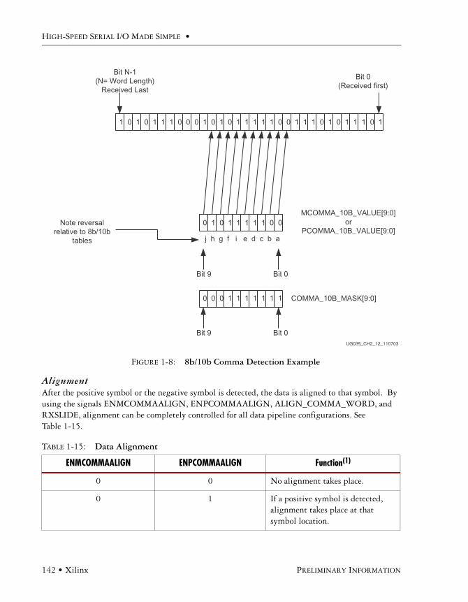
HIGH-SPEED SERIAL I/O MADE SIMPLE •
142 • Xilinx PRELIMINARY INFORMATION
AlignmentAfter the positive symbol or the negative symbol is detected, the data is aligned to that symbol. By using the signals ENMCOMMAALIGN, ENPCOMMAALIGN, ALIGN_COMMA_WORD, and RXSLIDE, alignment can be completely controlled for all data pipeline configurations. See Table 1-15.
FIGURE 1-8: 8b/10b Comma Detection Example
TABLE 1-15: Data Alignment
ENMCOMMAALIGN ENPCOMMAALIGN Function(1)
0 0 No alignment takes place.
0 1 If a positive symbol is detected, alignment takes place at that symbol location.
UG035_CH2_12_110703
1 0 1 0 1 1 1 0 0 0 1 0 1 0 1 1 1 1 1 0 0 1 1 1 0 1 0 1 1 1 0 1
Bit 0(Received first)
Bit N-1(N= Word Length)
Received Last
0 1 0 1 1 1 1 1 0 0MCOMMA_10B_VALUE[9:0]
orPCOMMA_10B_VALUE[9:0]
Bit 0Bit 9
0 0 0 1 1 1 1 1 1 1 COMMA_10B_MASK[9:0]
j h g f i e d c b a
Bit 0Bit 9
Note reversalrelative to 8b/10b
tables

SAMPLE SERDES DATA -- ROCKETIO X TRANSCEIVER OVERVIEW
PRELIMINARY INFORMATION XILINX • 143
ALIGN_COMMA_WORDThe attribute ALIGN_COMMA_WORD controls when realignment takes place when the difference between symbols is on a byte-by-byte basis. If the current position of the symbol detected is some frac-tion of a byte different than the previous symbol position, alignment takes place regardless of the set-ting of ALIGN_COMMA_WORD.
• There are three options for ALIGN_COMMA_WORD: 1 byte, 2 byte, and 4 byte. When ALIGN_COMMA_WORD is set to a 1, the detection circuit allows detection symbols in contiguous bytes. When ALIGN_COMMA_WORD is set to a 2, the detection circuit allows detection symbols every other byte. When ALIGN_COMMA_WORD is set to a 4, the detection circuit allows detection symbols every fourth byte (Figure 1-9).
1 0 If a negative symbol is detected, alignment takes place at that symbol location.
1 1 If a negative or positive symbol is detected, alignment takes place at that symbol location.
Notes: 1. The symbol mentioned is defined by P/MCOMMA_10B_VALUE.
16/20 32/40
1 byte alignment byte alignment
2 N/A 2-byte alignment
4 2-byte alignment 4-byte alignment
FIGURE 1-9: ALIGN_COMMA_WORD Diagram
TABLE 1-15: Data Alignment (Continued)
ENMCOMMAALIGN ENPCOMMAALIGN Function(1)
ALIGN_COMMA_WORD = 14 2 1 0
2
4
Four Byte Internal Two Byte Internal
Do not use
Note: Shaded blocks indicate where the comma can align to.ug035_ch2_13_051904
1 0

HIGH-SPEED SERIAL I/O MADE SIMPLE •
144 • Xilinx PRELIMINARY INFORMATION
RXSLIDERXSLIDE can be used to “slide” the aligned data by one bit. The RXSLIDE function when asserted High, increments the alignment by one bit, until it reaches the most significant bit, equal to the max-imum word length –1. When RXSLIDE is asserted High, it must be asserted Low for two clock peri-ods before it can be asserted High again. This functionality can be used for applications such as SONET.
64b/66bEncoder
BypassingThere are two types of bypassing regarding the 64b/66b encoder. The encoder block can either be entirely bypassed, or the 64b/66b encoder can be used and can be bypassed on a clock-by-clock basis.
If TXENC64B66BUSE is deasserted Low, the entire 64b/66b encoder is not used. If encoding is done in the fabric, the sync header [0:1] must be placed at TXCHARDISPVAL[0] and TXCHARD-ISPMODE[0] with the 32 TXDATA bits.
If TXENC64B66BUSE is asserted High, the TXBYPASS8B10B bit 0 signal bypasses the 64b/66b encoder on a clock basis, which means that two clock cycles are needed to do a full bypass of a block. The Sync Header is taken from the TXCHARDISPMODE[0:1]. To bypass on a block basis, the even boundary needs to be indicated at the fabric interface, which is contained in TXKERR bit 0. The TXCHARISK signal performs the function of TXC.
The transmit 64b/66b encoder borrows four bits of the TXCHARISK bus (bits [3:0]) to convey the control signaling to the 64b/66b encoder. The four TXC bits track with the four bytes of TXDATA_IN (TXC[0] with TXDATA_IN[7:0], and so on) to signal data block formatting. The transmit fabric interface logic (which first monitors transmit data as it travels from the fabric interface to the PMA) drives the encoder with the four TXC bits as follows:
TABLE 1-16: 64b/66b Bypassing
Signal Function
TXENC64B66BUSE 0 entire 64b/66b encoder bypassed
1 bypass on a clock-to-clock basis
TXBYPASS8B10B[0] Function 64b/66b clock-to-clock bypass
Function 64b/66b entirely bypassed
0 indicates no bypass defined by Table 1-18
1 indicates bypass this block
TXCHARDISPMODE[0:1]
Sync Header shown in Figure 1-11 (same as SH[0:1])
TXKERR[3] indicates even boundary for bypassing on block basis
TXCHARISK[3:0] performs function of TXC indicates character is a (K) control character

SAMPLE SERDES DATA -- ROCKETIO X TRANSCEIVER OVERVIEW
PRELIMINARY INFORMATION XILINX • 145
Each “one” in the TXC span represents a control-character-match -- recognition that the associ-ated byte is a special control character of some type (idle, start, terminate, or ordered-set).
Normal OperationThe 64b/66b encoder implements the Encoding Block Format function shown in Figure 1-11.
TABLE 1-17: Transmit 64b/66b Encoder Control Mapping
TXC[3:0] (TXCHARISK[3:0]) Block Formatting
1111 Idles OR terminate-with-idles
0001 Start-of-frame OR ordered-set
1110 Terminate in second position
1100 Terminate in third position
1000 Terminate in fourth position
0000 Data OR error (no k-chars)
FIGURE 1-10: Block Format Function
D0 D1 D2 D3 D4 D5 D6 T7 10
10D0 D1 D2 D3 D4 D5 T6 C7
10D0 D1 D2 D3 D4 T5 C6 C7
10D0 D1 D2 D3 T4 C5 C6 C7
10D0 D1 D2 T3 C4 C5 C6 C7
10D0 D1 T2 C3 C4 C5 C6 C7
10D0 T1 C2 C3 C4 C5 C6 C7
10T0 C1 C2 C3 C4 C5 C6 C7
10O0 D1 D2 D3 C4 C5 C6 C7
10O0 D1 D2 D3 O4 D5 D6 D7
10O0 D1 D2 D3 S4 D5 D6 D7
10C0 C1 C2 C3 S4 D5 D6 D7
10C0 C1 C2 C3 O4 D5 D6 D7
10C0 C1 C2 C3 C4 C5 C6 C7
01D0 D1 D2 D3 D4 D5 D6 D7
10S0 D1 D2 D3 D4 D5 D6 D7
Control Block FormatsBlock TypeField
Data Block Format
Bit Position
0x1e
0x2d
0x33
0x66
0x55
0x78
0x4b
0x87
0x99
0xaa
0xb4
0xcc
0xd2
D0
D0
Input Data Sync
Block Payload
01 2 65
D0 D1 D2 D3 D4 D5 D6 D7
D1
D1
D1
D1 D2
D2
C1 C2
C2
C4 C5
C5
C5
C5 C6
C6
C6
C6 C7
C7
C7
C7
C3
C2 C3 C4 C5 C6 C7C1C0
C1C0
C3 C4
C4
C4
O0
O0 O4
O4
C3
D0 C5 C6 C7C4C3C2
0xff D0 D1 D2 D3 D4 D5 D6
0xe1 D0 D1 C7D3 D4 D5D2
D0 D1 C6 C7D3 D4D2
D5 D6
D6 D7
D7
C3C1C0 C2 D6 D7D5
D5
D0 D1 C5 C6 C7D3D2
D2
D3
D1 D2 D6 D7D5D4D3
D3
D1 D2 O0 D6 D7D5D3
UG035_ch3_23_091103

HIGH-SPEED SERIAL I/O MADE SIMPLE •
146 • Xilinx PRELIMINARY INFORMATION
The control codes are specified as follows in Table 1-18:
Scrambler
BypassingIf the signal TXSCRAM64B66BUSE is deasserted Low, the scrambler is not used. Note that the scrambler operates on the read side of the transmit FIFO.
Normal OperationIf the signal TXSCRAM64B66BUSE is asserted High, the scrambler is enabled for use. The scrambler uses the polynomial:
TABLE 1-18: Control Codes
Control Character Notation XGMII
Control Code10GBASE-R Control Code
10GBASE-R0 Code
8b/10b Code
idle /I/ 0x07 0x00 K28.0 or K28.3 or
K28.5
start /S/ 0xfb Encoded by block type
field
K27.7
terminate /T/ 0xfd Encoded by block type
field
K29.7
error /E/ 0xfe 0x1e K30.7
Sequence ordered_set
/Q/ 0x9c Encoded by block type
field plus O mode
0x0 K28.4
reserved0 /R/ 0x1c 0x2d K28.0
reserved1 0x3c 0x33 K28.1
reserved2 /N/ 0x7c 0x4b K28.3
reserved3 /K/ 0xbc 0x55 K28.5
reserved4 0xdc 0x66 K28.6
reserved5 0xf7 0x78 K23.7
Signal ordered_set
/Fsig/ 0x5c Encoded by block type
field plus O mode
0xF K28.2

SAMPLE SERDES DATA -- ROCKETIO X TRANSCEIVER OVERVIEW
PRELIMINARY INFORMATION XILINX • 147
G(x) = 1 + x39 + x58
to scramble 64b/66b payload data. The scrambler works in conjunction with the gearbox to scramble and format data correctly.
When using the 64b/66b scrambler, the Gearbox must also be enabled (Always set to TXSCRAM64BB66USE = TXGEARBOX64B66BUSE)
Gearbox
BypassingIf the signal TXGEARBOX64B66BUSE is deasserted Low, the gearbox is not used. The gearbox should always be enabled when using the 64b/66b protocol.
Normal OperationIf the signal TXGEARBOX64B66BUSE is asserted High, the gear box is enabled. The gearbox frames 64b/66b data for the PMA.
Decoder
BypassingIf RXDEC64B66BUSE is deasserted Low, the entire 64b/66b decoder is not used.
Normal OperationIf RXDEC64B66BUSE is asserted High, the 64b/66b decoder decodes according to the 64b/66b block format table shown in Figure 1-7.
If the signal RXIGNOREBTF is asserted High, block type fields not recognized are passed on, whereas if the signal is asserted Low, the error block /E/ is passed on. RXCHARISK is equivalent to RXC when the decoder is enabled.
TXSCRAM64B66BUSE 0 scrambler not used
1 scrambler enabled
TXGEARBOX64B66BUSE 0
1 always set to ‘1’ when scrambler and descrambler are enabled.
RXDEC64B66BUSE 0 decoder not used
1 decoder used
HIGH-SPEED SERIAL I/O MADE SIMPLE •
148 • Xilinx PRELIMINARY INFORMATION
Descrambler
BypassingIf the signal RXDESCRAM64B66BUSE is deasserted Low, the descrambler is not used.
Normal OperationIf the signal RXDESCRAM64B66BUSE is asserted High, the descrambler is enabled for use. The descrambler uses the polynomial:
G(x) = 1 + x39 + x58
Block Sync
Normal OperationThis block sync design works hand-in-hand with the commaDet block. The commaDet takes as input 32 bits of scrambled and unaligned data from the PMA. It then sends to the block sync the 2-bit sync header, or what it thinks is the sync header based on the current tag value. It asserts test_sh which tells the block sync to test the value of the sync header. The block sync analyzes the sync header and if it is valid, increments the sh_cnt counter. If the sync header is not a legal value, sh_cnt is incre-mented as well as the counter sh_invalid_cnt, and then bit_slip is asserted for one clock. The bit slip signal feeds back to the commaDet block and tells it to shift the barrel shifter by one bit. This process of slipping and testing the sync header repeats until block lock is achieved.
RXIGNOREBTF Function 64b/66b decoder used
Function 64b/66b decoder bypassed
0 unrecognized field types cause /E/ passed on
Undefined
1 unrecognized field types passed on
RXCHARISK Equivalent to RXC Defined by 8b/10b decoder use

SAMPLE SERDES DATA -- ROCKETIO X TRANSCEIVER OVERVIEW
PRELIMINARY INFORMATION XILINX • 149
FIGURE 1-11: Block Sync State Machine
LOCK_INIT
block_lock <=falsetest_sh <= false
RESET_CNT
sh_cnt <= 0sh_invalid_cnt <= 0slip_done <= false
TEST_SH
test_sh <=false
VALID_SH
sh_cnt ++
64_GOOD
block_lock <=true
SLIP
block_lock <=falseSLIP <=true
INVALID_SH
sh_cnt ++sh_invalid_cnt ++
sh_cnt = 64*sh_invalid_cnt = 0
sh_cnt = 64*sh_invalid_cnt > 0
sh_cnt = 64*sh_invalid_cnt < 16*block_lock sh_invalid_cnt = 16 +
!block_lock
slip_done
!sh_valid
UCT
sh_validtest_sh*sh_cnt < 64
test_sh
UCT
test_sh*sh_cnt < 64*sh_invalid_cnt < 16*block_lock
ug035_ch3_21_090903

HIGH-SPEED SERIAL I/O MADE SIMPLE •
150 • Xilinx PRELIMINARY INFORMATION
The state machine works by keeping track of valid and invalid sync headers. Upon reset, block lock is deasserted, and the state is LOCK_INIT. The next state is RESET_CNT where all counters are zeroed out. When test_sh is asserted, the next state is TEST_SH, which checks the validity of the sync header. If it is valid, the next state is VALID_SH, if not, the state changes to INVALID_SH.
From VALID_SH, if sh_cnt is less than the attribute value sh_cnt_max and test_sh is High, the next state is TEST_SH. If sh_cnt is equal to sh_cnt_max and sh_invalid_cnt equals 0, the next state is GOOD_64 and from there block_lock is asserted. Then the process repeats again and the counters are zeroed.
If at TEST_SH sh_cnt equals sh_cnt_max, but sh_invalid_cnt is greater than zero, then the next state is RESET_CNT. From INVALID_SH, if sh_invalid_cnt equals sh_invalid_cnt_max, or if block_lock is not asserted, the next state is SLIP, where bit_slip is asserted, and then on to RESET_CNT. If sh_cnt equals sh_cnt_max and sh_invalid_cnt is less than sh_invalid_cnt_max and block_lock is asserted, then go back to RESET_CNT with-out changing block_lock or bit_slip.
Finally, if test_sh is High and sh_cnt is less than sh_cnt_max, and sh_invalid_cnt is less than sh_invalid_cnt_max and block_lock is asserted, go back to the TEST_SH state. The main thing to note with this state machine is that to achieve block lock, one must receive sh_cnt_max number of valid sync headers in a row without getting an invalid sync header. However, once block lock is achieved, sh_invalid_cnt_max -1 number of invalid sync headers can be received within sh_cnt_max number of valid sync headers. Thus, once locked, it is harder to break lock.
Functions Common to All ProtocolsClock CorrectionClock correction is needed when the rate that data is fed into the write side of the receive FIFO is either slower or faster than the rate that data is retrieved from the read side of the receive FIFO. The rate of write data entering the FIFO is determined by the frequency of RXRECCLK. The rate of read data retrieved from the read side of the FIFO is determined by the frequency of RXUSRCLK.
There is one clock correction mode: Append/Remove Idle Clock Correction.
Append/Remove Idle Clock CorrectionWhen the attribute CLK_COR_SEQ_DROP is asserted Low and CLK_CORRECT_USE is asserted hIgh, the Append/remove Idle Clock Correction mode is enabled.
The Append/remove Idle Clock Correction mode corrects for differing clock rates by finding idles in the bitstream, and then either appending or removing idles at the point where the idles were found.
There are a few attributes that need to be set by the user so that the append/remove function can be used correctly. The attribute CLK_COR_MAX_LAT sets the maximum latency through the receive FIFO. If the latency through the receive FIFO exceeds this value, idles are removed so that latency through the receive FIFO is less than CLK_COR_MAX_LAT.
The attribute CLK_COR_MIN_LAT sets the minimum latency through the receive FIFO. If the latency through the receive FIFO is less than this value, idles are inserted so that the latency through the receive FIFO are greater than CLK_COR_MIN_LAT. A correction to the latency due to a CLK_COR_MAX_LAT violation is never less than CLK_COR_MIN_LAT. This is also true for a cor-rection to the latency due to a CLK_COR_MIN_LAT violation; the resulting latency after the correc-tion is greater than CLK_COR_MAX_LAT.

SAMPLE SERDES DATA -- ROCKETIO X TRANSCEIVER OVERVIEW
PRELIMINARY INFORMATION XILINX • 151
Clock Correction SequencesSearching within the bitstream for an idle is the core function of the clock correction circuit. The detection of idles starts the correction procedure.
Idles the clock correction circuit should detect are specified by the lower 10 bits of the attributes:• CLK_COR_SEQ_1_1• CLK_COR_SEQ_1_2• CLK_COR_SEQ_1_3• CLK_COR_SEQ_1_4• CLK_COR_SEQ_2_1• CLK_COR_SEQ_2_2• CLK_COR_SEQ_2_3• CLK_COR_SEQ_2_4The 11th bit of each clock correction sequence attribute determines either an 8- or 10-bit com-
pare.Detection of the clock correction sequence in the bitstream is specified by eight words consisting
of 10 bits each. Clock correction sequences can have lengths of 1, 2, 3, 4, or 8 bytes. When the length specified by the user is between 1 and 4, CLK_COR_SEQ_1_* holds the first
pattern to be searched for. CLK_COR_SEQ_1_1 is the least significant byte, which is transmitted first from the transmitter and detected first in the receiver. If CLK_COR_SEQ_2_USE is asserted High when the length is between 1 and 4, the sequence specified by CLK_COR_SEQ_2_* is specified as a second pattern to match. In that case, the pattern specified by sequence 1 or sequence 2 matches as a clock correction sequence.
The CLK_COR_SEQ_MASK must have the bits set to a logic 1 mask off the 2 or 3 unusedbytes.
When the length specified by the user is eight, CLK_COR_SEQ_1_* holds the first four bytes, while CLK_COR_SEQ_2_* holds the last four bytes. CLK_COR_SEQ_1_1 is the least significant byte, which is transmitted first from the transmitter and detected first in the receiver. CLK_COR__SEQ_2_USE must be asserted High.
The clock correction sequence is a special sequence to accommodate frequency differences between the received data (as reflected in RXRECCLK) and RXUSRCLK. Most of the primitives have these defaulted to the respective protocols. Only the GT_CUSTOM allows this sequence to be set to any specific protocol. The sequence contains 11 bits including the 10 bits of serial data. The 11th bit has two different formats. The typical usage is:
• 0, disparity error required, char is K, 8-bit data value (after 8b/10b decoding, depends on CLK_COR_8B10B_DE)
• 0, 10-bit data value (without 8b/10b decoding, depends on CLK_COR_8B10B_DE)• 1, xx, sync character (with 64b/66b encoding• 1, xx, 8-bit data value

HIGH-SPEED SERIAL I/O MADE SIMPLE •
152 • Xilinx PRELIMINARY INFORMATION
Table 1-19 is an example of data 11-bit attribute setting, the character value, CHARISK value, and the parallel data interface, and how each corresponds with the other.
Determining Correct CLK_COR_MIN_LAT To determine the correct CLK_COR_MIN_LAT value, several requirements must be met.
• CLK_COR_MIN_LAT must be less than or equal to 12.• CLK_COR_MIN_LAT and CLK_COR_MAX_LAT must be multiples of CCS/CBS lengths
and ALIGN_COMMA_WORD.• For symbols less than 8 bytes, (CLK_COR_MIN_LAT – CHAN_BOND_LIMIT) > 12.
For symbols of 8 bytes, (CLK_COR_MIN_LAT – CHAN_BOND_LIMIT) > 16.
Channel BondingChannel bonding is the technique of tying several serial channels together to create one aggregate channel. Several channels are fed on the transmit side by one parallel bus and reproduced on the receive side as the identical parallel bus. The maximum number of serial differential pairs that can be bonded is 20. Channel bonding is supported by several primitives including GT10_CUSTOM, GT10_INFINIBAND, GT10_XAUI, and GT10_AURORA.
The channel bonding match logic finds CB characters across word boundaries and performs a “comma” style realignment of the data. The data path is byte scrambled until reset as shown below in the example (additional comma alignments will not realign the data). As a result, users should be care-ful when picking channel bonding characters and should use, in general, special characters that cannot appear in the normal data stream.
Example:
The channel bond character is 0x000000FF. If this sequence of data is sent:
000000FF 01020304 05060708 09000000 FF010203 04050607
The result is:
000000FF
TABLE 1-19: Clock Correction Sequence/Data Correlation for 16-Bit Data Port
Attribute Setting Character CHARISK TXDATA (hex)
CLK_COR_SEQ_1_1 = 00110111100 K28.5 1 BC
CLK_COR_SEQ_1_2 = 00010010101 D21.4 0 95
CLK_COR_SEQ_1_3 = 00010110101 D21.5 0 B5
CLK_COR_SEQ_1_4 = 00010110101 D21.5 0 B5
Notes: 1. CLK_COR_8B10B_DE = TRUE.

SAMPLE SERDES DATA -- ROCKETIO X TRANSCEIVER OVERVIEW
PRELIMINARY INFORMATION XILINX • 153
01020304 05060708 000000FF 01020304 050607xx The bonded channels consist of one master transceiver and 1 to 19 slave transceivers. The
CHBONDI/CHBONDO buses of the transceivers are daisy-chained together as shown in Figure 1-12.
When the master transceiver detects a channel bond alignment sequence in its data stream, it sig-nals the slave to perform channel bonding by driving its CHBONDO bus as follows in Table 1-20:
TABLE 1-20: Channel Bond Alignment Sequence
Detected CHBONDO Bus
No Channel Bond XX0002
Channel Bond - Byte 0 XX1002
Channel Bond - Byte 1 XX1012
Channel Bond - Byte 2 XX1102
Channel Bond - Byte 3 XX1112

HIGH-SPEED SERIAL I/O MADE SIMPLE •
154 • Xilinx PRELIMINARY INFORMATION
Whether a slave is a 1-hop or 2-hop slave, internal logic causes the data driven on the CHBONDO bus from the master to be recognized by the slaves at the same time and must be deter-ministic. Therefore, it is important that the interconnect of CHBONDO-to-CHBONDI not contain any pipeline stages. The data must transfer from CHBONDO to CHBONDI in one clock.
The data streams input to the channel bonded transceivers can be skewed in time from each other. The maximum byte skew that the channel bond logic should allow is set by the attribute MC_CHAN_BOND_LIMIT. During the channel bond operation, the slave receives notification of the master's alignment code location via the CHBONDO bus. If a slave detects the position of its alignment code to be outside the window of CHAN_BOND_LIMIT from the master, then the slave does not perform the channel bond and sets a channel bond error flag. If the channel bond is successful, the slave outputs its skew relative to the master. The skew and channel bond error flag are available on the RXBUFSTATUS bus.
For place and route, the transceiver has one restriction. This is required when channel bonding is implemented. Because of the delay limitations on the CHBONDO to CHBONDI ports, linking of the Master to a Slave_1_hop must run either in the X or Y direction, but not both.
FIGURE 1-12: Daisy-Chained Transceiver CHBONDI/CHBONDO Buses
CHBONDI
CHBONDI
CHBONDI
CHBONDO
SLAVE
MASTER
CHBONDOCHBONDI CHBONDO
SLAVE
CHBONDO
SLAVE
CHBONDI CHBONDO
SLAVE
CHBONDI CHBONDO
SLAVE
CHBONDI CHBONDO
SLAVE
2-Hop Slaves
1-Hop Slaves
UG035_ch3_20_012704
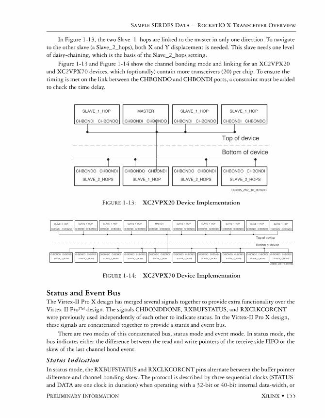
SAMPLE SERDES DATA -- ROCKETIO X TRANSCEIVER OVERVIEW
PRELIMINARY INFORMATION XILINX • 155
In Figure 1-13, the two Slave_1_hops are linked to the master in only one direction. To navigate to the other slave (a Slave_2_hops), both X and Y displacement is needed. This slave needs one level of daisy-chaining, which is the basis of the Slave_2_hops setting.
Figure 1-13 and Figure 1-14 show the channel bonding mode and linking for an XC2VPX20 and XC2VPX70 devices, which (optionally) contain more transceivers (20) per chip. To ensure the timing is met on the link between the CHBONDO and CHBONDI ports, a constraint must be added to check the time delay.
Status and Event BusThe Virtex-II Pro X design has merged several signals together to provide extra functionality over the Virtex-II Pro™ design. The signals CHBONDDONE, RXBUFSTATUS, and RXCLKCORCNT were previously used independently of each other to indicate status. In the Virtex-II Pro X design, these signals are concatenated together to provide a status and event bus.
There are two modes of this concatenated bus, status mode and event mode. In status mode, the bus indicates either the difference between the read and write pointers of the receive side FIFO or the skew of the last channel bond event.
Status IndicationIn status mode, the RXBUFSTATUS and RXCLKCORCNT pins alternate between the buffer pointer difference and channel bonding skew. The protocol is described by three sequential clocks (STATUS and DATA are one clock in duration) when operating with a 32-bit or 40-bit internal data-width, or
FIGURE 1-13: XC2VPX20 Device Implementation
FIGURE 1-14: XC2VPX70 Device Implementation
UG035_ch2_10_091603
CHBONDI CHBONDO
SLAVE_1_HOP
CHBONDO CHBONDI
SLAVE_2_HOPS
CHBONDI CHBONDO
SLAVE_1_HOP
CHBONDO CHBONDI
SLAVE_2_HOPS
CHBONDO CHBONDI
SLAVE_2_HOPS
CHBONDO CHBONDI
SLAVE_1_HOP
CHBONDI CHBONDO
MASTER
CHBONDI CHBONDO
SLAVE_1_HOP
Top of device
Bottom of device
UG035_ch2_11_051904
CHBONDI CHBONDO
SLAVE_1_HOP
CHBONDO CHBONDI
SLAVE_2_HOPS
CHBONDI CHBONDO
SLAVE_1_HOP
CHBONDO CHBONDI
SLAVE_2_HOPS
CHBONDI CHBONDO
SLAVE_1_HOP
CHBONDO CHBONDI
SLAVE_2_HOPS
CHBONDI CHBONDO
SLAVE_1_HOP
CHBONDO CHBONDI
SLAVE_2_HOPS
CHBONDI CHBONDO
SLAVE_1_HOP
CHBONDO CHBONDI
SLAVE_2_HOPS
CHBONDO CHBONDI
SLAVE_2_HOPS
CHBONDI CHBONDO
SLAVE_1_HOP
CHBONDO CHBONDI
SLAVE_2_HOPS
CHBONDO CHBONDI
SLAVE_1_HOP
CHBONDI CHBONDO
MASTER
CHBONDI CHBONDO
SLAVE_1_HOP
Top of device
Bottom of device
CHBONDI CHBONDO
SLAVE_1_HOP
CHBONDO CHBONDI
SLAVE_2_HOPS
CHBONDI CHBONDO
SLAVE_1_HOP
CHBONDO CHBONDI
SLAVE_2_HOPS
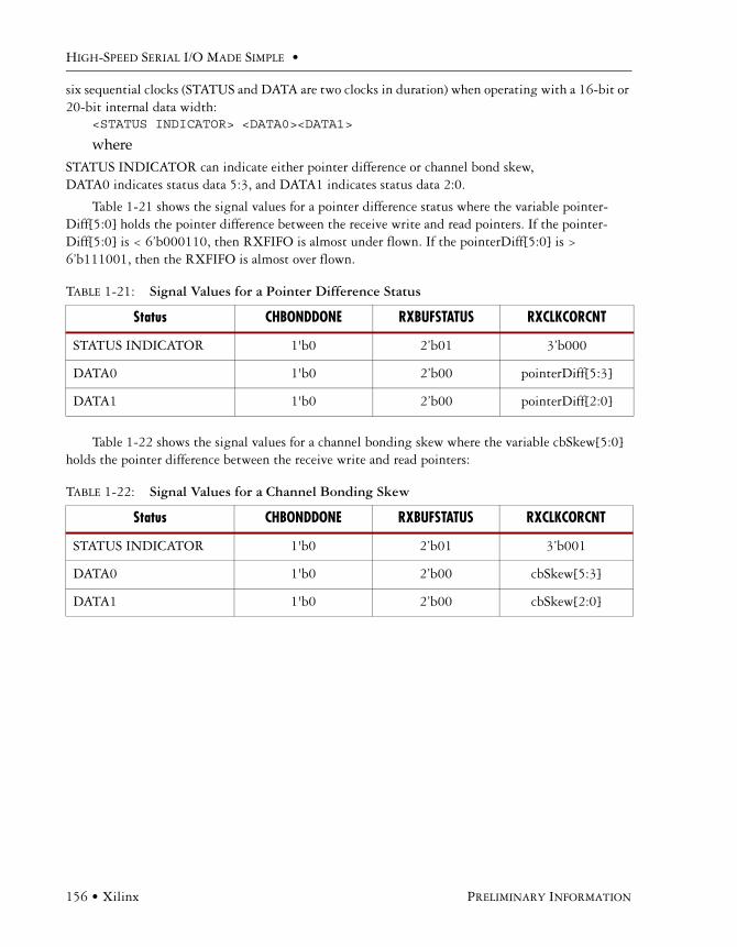
HIGH-SPEED SERIAL I/O MADE SIMPLE •
156 • Xilinx PRELIMINARY INFORMATION
six sequential clocks (STATUS and DATA are two clocks in duration) when operating with a 16-bit or 20-bit internal data width:
<STATUS INDICATOR> <DATA0><DATA1>
where STATUS INDICATOR can indicate either pointer difference or channel bond skew,DATA0 indicates status data 5:3, and DATA1 indicates status data 2:0.
Table 1-21 shows the signal values for a pointer difference status where the variable pointer-Diff[5:0] holds the pointer difference between the receive write and read pointers. If the pointer-Diff[5:0] is < 6’b000110, then RXFIFO is almost under flown. If the pointerDiff[5:0] is > 6’b111001, then the RXFIFO is almost over flown.
Table 1-22 shows the signal values for a channel bonding skew where the variable cbSkew[5:0] holds the pointer difference between the receive write and read pointers:
TABLE 1-21: Signal Values for a Pointer Difference Status
Status CHBONDDONE RXBUFSTATUS RXCLKCORCNT
STATUS INDICATOR 1'b0 2’b01 3’b000
DATA0 1'b0 2’b00 pointerDiff[5:3]
DATA1 1'b0 2’b00 pointerDiff[2:0]
TABLE 1-22: Signal Values for a Channel Bonding Skew
Status CHBONDDONE RXBUFSTATUS RXCLKCORCNT
STATUS INDICATOR 1'b0 2’b01 3’b001
DATA0 1'b0 2’b00 cbSkew[5:3]
DATA1 1'b0 2’b00 cbSkew[2:0]

SAMPLE SERDES DATA -- ROCKETIO X TRANSCEIVER OVERVIEW
PRELIMINARY INFORMATION XILINX • 157
Event IndicationTwo types of events can occur. See Table 1-23. When an event occurs, it can override a status indica-tion. An event can only last for one clock and can be signaled by CHBONDDONE asserting High, or RXBUFSTATUS equating to 2'b10.
An event will always override status, but after an event is completed, status will continue toalternate between the pointer difference and the channel bond skew.
Sample VerilogThe following sample code is to determine underflow or overflow of the RX buffer when 32-bit or 40-bit internal data path is selected.:
module status_decoder ( RXUSRCLK2, DCM_LOCKED_N, PMARXLOCK, CHBONDDONE, RXBUFSTATUS, RXCLKCORCNT,
cc_event_insert, // Clock Correction Insertion Event cc_event_remove, // Clock Correction Removal Event cb_event_load, // Channel Bonding Load Event err_event_cc, // Clock Correction Error Event err_event_cb, // Channel Bonding Error Event pointerDiff, // RX Elastic Buffer Pointer Difference rxbuf_almost_err, // RX Elastic Buffer Almost Error cbSkew); input RXUSRCLK2; input DCM_LOCKED_N; input PMARXLOCK; input CHBONDDONE; input [1:0] RXBUFSTATUS; input [2:0] RXCLKCORCNT; output cc_event_insert; output cc_event_remove; output cb_event_load; output err_event_cc;
TABLE 1-23: Signal Values for Event Indication
Event CHBONDDONE RXBUFSTATUS RXCLKCORCNT
Channel Bond Load 1'b1 2’b00 3’b111
Clock Correction 1'b0 2’b10 3’bxxx
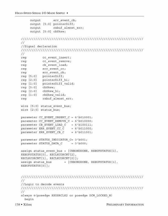
HIGH-SPEED SERIAL I/O MADE SIMPLE •
158 • Xilinx PRELIMINARY INFORMATION
output err_event_cb; output [5:0] pointerDiff; output rxbuf_almost_err; output [5:0] cbSkew;
////////////////////////////////////////////////////////////////////////Signal declaration //////////////////////////////////////////////////////////////////////reg cc_event_insert; reg cc_event_remove; reg cb_event_load; reg err_event_cc; reg err_event_cb; reg [5:0] pointerDiff; reg [2:0] pointerDiff_hi; reg [1:0] pointerDiff_valid; reg [5:0] cbSkew; reg [2:0] cbSkew_hi; reg [1:0] cbSkew_valid; reg rxbuf_almost_err;
wire [5:0] status_event_bus; wire [2:0] status_bus;
parameter CC_EVENT_INSERT_C = 6'b010001; parameter CC_EVENT_REMOVE_C = 6'b010000; parameter CB_EVENT_LOAD_C = 6'b100111; parameter ERR_EVENT_CC_C = 6'b011000; parameter ERR_EVENT_CB_C = 6'b011001;
parameter STATUS_INDICATOR_C= 3'b001; parameter STATUS_DATA_C = 3'b000;
assign status_event_bus = {CHBONDDONE, RXBUFSTATUS[1], RXBUFSTATUS[0], RXCLKCORCNT[2],RXCLKCORCNT[1], RXCLKCORCNT[0]}; assign status_bus = {CHBONDDONE, RXBUFSTATUS[1], RXBUFSTATUS[0]};
////////////////////////////////////////////////////////////////////////Logic to decode events //////////////////////////////////////////////////////////////////////always @(posedge RXUSRCLK2 or posedge DCM_LOCKED_N) begin

SAMPLE SERDES DATA -- ROCKETIO X TRANSCEIVER OVERVIEW
PRELIMINARY INFORMATION XILINX • 159
if (DCM_LOCKED_N) begin cc_event_insert <= 1'b0; cc_event_remove <= 1'b0; cb_event_load <= 1'b0; err_event_cc <= 1'b0; err_event_cb <= 1'b0; end else begin cc_event_insert <= status_event_bus == CC_EVENT_INSERT_C; cc_event_remove <= status_event_bus == CC_EVENT_REMOVE_C; cb_event_load <= status_event_bus == CB_EVENT_LOAD_C; err_event_cc <= status_event_bus == ERR_EVENT_CC_C; err_event_cb <= status_event_bus == ERR_EVENT_CB_C; end end
//////////////////////////////////////////////////////////////////////// Logic to decode the cbSkew value and pointerDiff value //////////////////////////////////////////////////////////////////////always @(posedge RXUSRCLK2 or posedge DCM_LOCKED_N) begin if (DCM_LOCKED_N) begin pointerDiff_valid <= 2'b00; cbSkew_valid <= 2'b00; end else if ((status_bus == STATUS_INDICATOR_C) & ~RXCLKCORCNT[2] & ~RXCLKCORCNT[1] ) begin pointerDiff_valid <= {1'b0, ~RXCLKCORCNT[0]}; cbSkew_valid <= {1'b0, RXCLKCORCNT[0]}; end else if (status_bus == STATUS_DATA_C) begin pointerDiff_valid[1] <= pointerDiff_valid[0]; pointerDiff_valid[0] <= 1'b0; cbSkew_valid[1] <= cbSkew_valid[0]; cbSkew_valid[0] <= 1'b0; end else begin // clear the valid signal if the status is interrupted by an event. pointerDiff_valid <= 2'b00; cbSkew_valid <= 2'b00; end end
always @(posedge RXUSRCLK2 or posedge DCM_LOCKED_N) begin

HIGH-SPEED SERIAL I/O MADE SIMPLE •
160 • Xilinx PRELIMINARY INFORMATION
if (DCM_LOCKED_N || ~PMARXLOCK) begin // reset the value to neutral position pointerDiff <= 32; pointerDiff_hi <= 4; cbSkew <= 32; cbSkew_hi <= 4; end else if (status_bus == STATUS_DATA_C) begin if (pointerDiff_valid[0]) // register higher 3 bits pointerDiff_hi <= RXCLKCORCNT; else if (pointerDiff_valid[1]) // update entire register when all 6 bits are acquired. pointerDiff <= {pointerDiff_hi , RXCLKCORCNT}; if (cbSkew_valid[0]) // register higher 3 bits cbSkew_hi <= RXCLKCORCNT; else if (cbSkew_valid[1]) // update entire register when all 6 bits are acquired. cbSkew <= {cbSkew_hi , RXCLKCORCNT}; end end //////////////////////////////////////////////////////////////////////// Generate RX Elastic Buffer almost error //////////////////////////////////////////////////////////////////////always @(posedge RXUSRCLK2 or posedge DCM_LOCKED_N) begin if (DCM_LOCKED_N) rxbuf_almost_err <= 1'b0; else rxbuf_almost_err <= (pointerDiff < 6) | (pointerDiff > 57); end
endmodule

PRELIMINARY INFORMATION XILINX • 161
CHAPTER 1
8b/10b Tables
This information was extracted from the RocketIO™ X Transceiver User Guide. For up-to-date information, please go to: http://www.xilinx.com/bvdocs/userguides/ug035.pdf
Valid Data and Control CharactersRocketIO X Transceiver 8b/10b encoding includes a set of Data characters and K-characters. Eight-bit values are coded into 10-bit values keeping the serial line DC balanced. K-characters are special Data characters designated with a CHARISK. K-characters are used for specific informative designa-tions. Table 1-1 and Table 1-2 show the Data and K tables of valid characters.
TABLE 1-1: Valid Data Characters
Data Byte Name Bits HGF EDCBA
Current RD –abcdei fghj
Current RD + abcdei fghj
D0.0 000 00000 100111 0100 011000 1011
D1.0 000 00001 011101 0100 100010 1011
D2.0 000 00010 101101 0100 010010 1011
D3.0 000 00011 110001 1011 110001 0100
D4.0 000 00100 110101 0100 001010 1011
D5.0 000 00101 101001 1011 101001 0100
D6.0 000 00110 011001 1011 011001 0100
D7.0 000 00111 111000 1011 000111 0100
D8.0 000 01000 111001 0100 000110 1011
D9.0 000 01001 100101 1011 100101 0100

HIGH-SPEED SERIAL I/O MADE SIMPLE •
162 • Xilinx PRELIMINARY INFORMATION
D10.0 000 01010 010101 1011 010101 0100
D11.0 000 01011 110100 1011 110100 0100
D12.0 000 01100 001101 1011 001101 0100
D13.0 000 01101 101100 1011 101100 0100
D14.0 000 01110 011100 1011 011100 0100
D15.0 000 01111 010111 0100 101000 1011
D16.0 000 10000 011011 0100 100100 1011
D17.0 000 10001 100011 1011 100011 0100
D18.0 000 10010 010011 1011 010011 0100
D19.0 000 10011 110010 1011 110010 0100
D20.0 000 10100 001011 1011 001011 0100
D21.0 000 10101 101010 1011 101010 0100
D22.0 000 10110 011010 1011 011010 0100
D23.0 000 10111 111010 0100 000101 1011
D24.0 000 11000 110011 0100 001100 1011
D25.0 000 11001 100110 1011 100110 0100
D26.0 000 11010 010110 1011 010110 0100
D27.0 000 11011 110110 0100 001001 1011
D28.0 000 11100 001110 1011 001110 0100
D29.0 000 11101 101110 0100 010001 1011
D30.0 000 11110 011110 0100 100001 1011
D31.0 000 11111 101011 0100 010100 1011
D0.1 001 00000 100111 1001 011000 1001
D1.1 001 00001 011101 1001 100010 1001
D2.1 001 00010 101101 1001 010010 1001
TABLE 1-1: Valid Data Characters (Continued)
Data Byte Name Bits HGF EDCBA
Current RD –abcdei fghj
Current RD + abcdei fghj

8B/10B TABLES
PRELIMINARY INFORMATION XILINX • 163
D3.1 001 00011 110001 1001 110001 1001
D4.1 001 00100 110101 1001 001010 1001
D5.1 001 00101 101001 1001 101001 1001
D6.1 001 00110 011001 1001 011001 1001
D7.1 001 00111 111000 1001 000111 1001
D8.1 001 01000 111001 1001 000110 1001
D9.1 001 01001 100101 1001 100101 1001
D10.1 001 01010 010101 1001 010101 1001
D11.1 001 01011 110100 1001 110100 1001
D12.1 001 01100 001101 1001 001101 1001
D13.1 001 01101 101100 1001 101100 1001
D14.1 001 01110 011100 1001 011100 1001
D15.1 001 01111 010111 1001 101000 1001
D16.1 001 10000 011011 1001 100100 1001
D17.1 001 10001 100011 1001 100011 1001
D18.1 001 10010 010011 1001 010011 1001
D19.1 001 10011 110010 1001 110010 1001
D20.1 001 10100 001011 1001 001011 1001
D21.1 001 10101 101010 1001 101010 1001
D22.1 001 10110 011010 1001 011010 1001
D23.1 001 10111 111010 1001 000101 1001
D24.1 001 11000 110011 1001 001100 1001
D25.1 001 11001 100110 1001 100110 1001
D26.1 001 11010 010110 1001 010110 1001
D27.1 001 11011 110110 1001 001001 1001
D28.1 001 11100 001110 1001 001110 1001
TABLE 1-1: Valid Data Characters (Continued)
Data Byte Name Bits HGF EDCBA
Current RD –abcdei fghj
Current RD + abcdei fghj
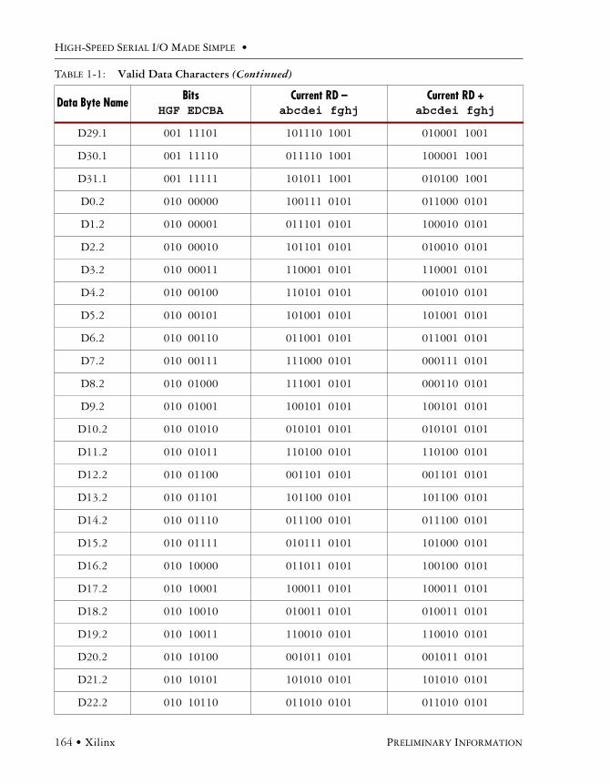
HIGH-SPEED SERIAL I/O MADE SIMPLE •
164 • Xilinx PRELIMINARY INFORMATION
D29.1 001 11101 101110 1001 010001 1001
D30.1 001 11110 011110 1001 100001 1001
D31.1 001 11111 101011 1001 010100 1001
D0.2 010 00000 100111 0101 011000 0101
D1.2 010 00001 011101 0101 100010 0101
D2.2 010 00010 101101 0101 010010 0101
D3.2 010 00011 110001 0101 110001 0101
D4.2 010 00100 110101 0101 001010 0101
D5.2 010 00101 101001 0101 101001 0101
D6.2 010 00110 011001 0101 011001 0101
D7.2 010 00111 111000 0101 000111 0101
D8.2 010 01000 111001 0101 000110 0101
D9.2 010 01001 100101 0101 100101 0101
D10.2 010 01010 010101 0101 010101 0101
D11.2 010 01011 110100 0101 110100 0101
D12.2 010 01100 001101 0101 001101 0101
D13.2 010 01101 101100 0101 101100 0101
D14.2 010 01110 011100 0101 011100 0101
D15.2 010 01111 010111 0101 101000 0101
D16.2 010 10000 011011 0101 100100 0101
D17.2 010 10001 100011 0101 100011 0101
D18.2 010 10010 010011 0101 010011 0101
D19.2 010 10011 110010 0101 110010 0101
D20.2 010 10100 001011 0101 001011 0101
D21.2 010 10101 101010 0101 101010 0101
D22.2 010 10110 011010 0101 011010 0101
TABLE 1-1: Valid Data Characters (Continued)
Data Byte Name Bits HGF EDCBA
Current RD –abcdei fghj
Current RD + abcdei fghj
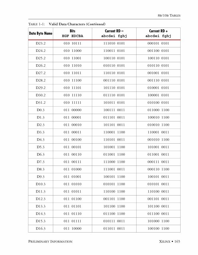
8B/10B TABLES
PRELIMINARY INFORMATION XILINX • 165
D23.2 010 10111 111010 0101 000101 0101
D24.2 010 11000 110011 0101 001100 0101
D25.2 010 11001 100110 0101 100110 0101
D26.2 010 11010 010110 0101 010110 0101
D27.2 010 11011 110110 0101 001001 0101
D28.2 010 11100 001110 0101 001110 0101
D29.2 010 11101 101110 0101 010001 0101
D30.2 010 11110 011110 0101 100001 0101
D31.2 010 11111 101011 0101 010100 0101
D0.3 011 00000 100111 0011 011000 1100
D1.3 011 00001 011101 0011 100010 1100
D2.3 011 00010 101101 0011 010010 1100
D3.3 011 00011 110001 1100 110001 0011
D4.3 011 00100 110101 0011 001010 1100
D5.3 011 00101 101001 1100 101001 0011
D6.3 011 00110 011001 1100 011001 0011
D7.3 011 00111 111000 1100 000111 0011
D8.3 011 01000 111001 0011 000110 1100
D9.3 011 01001 100101 1100 100101 0011
D10.3 011 01010 010101 1100 010101 0011
D11.3 011 01011 110100 1100 110100 0011
D12.3 011 01100 001101 1100 001101 0011
D13.3 011 01101 101100 1100 101100 0011
D14.3 011 01110 011100 1100 011100 0011
D15.3 011 01111 010111 0011 101000 1100
D16.3 011 10000 011011 0011 100100 1100
TABLE 1-1: Valid Data Characters (Continued)
Data Byte Name Bits HGF EDCBA
Current RD –abcdei fghj
Current RD + abcdei fghj
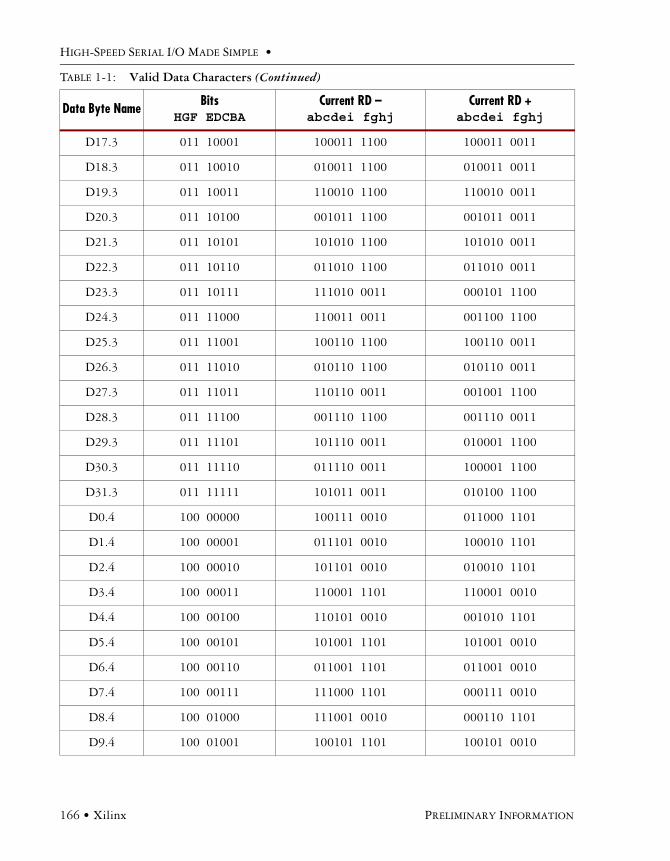
HIGH-SPEED SERIAL I/O MADE SIMPLE •
166 • Xilinx PRELIMINARY INFORMATION
D17.3 011 10001 100011 1100 100011 0011
D18.3 011 10010 010011 1100 010011 0011
D19.3 011 10011 110010 1100 110010 0011
D20.3 011 10100 001011 1100 001011 0011
D21.3 011 10101 101010 1100 101010 0011
D22.3 011 10110 011010 1100 011010 0011
D23.3 011 10111 111010 0011 000101 1100
D24.3 011 11000 110011 0011 001100 1100
D25.3 011 11001 100110 1100 100110 0011
D26.3 011 11010 010110 1100 010110 0011
D27.3 011 11011 110110 0011 001001 1100
D28.3 011 11100 001110 1100 001110 0011
D29.3 011 11101 101110 0011 010001 1100
D30.3 011 11110 011110 0011 100001 1100
D31.3 011 11111 101011 0011 010100 1100
D0.4 100 00000 100111 0010 011000 1101
D1.4 100 00001 011101 0010 100010 1101
D2.4 100 00010 101101 0010 010010 1101
D3.4 100 00011 110001 1101 110001 0010
D4.4 100 00100 110101 0010 001010 1101
D5.4 100 00101 101001 1101 101001 0010
D6.4 100 00110 011001 1101 011001 0010
D7.4 100 00111 111000 1101 000111 0010
D8.4 100 01000 111001 0010 000110 1101
D9.4 100 01001 100101 1101 100101 0010
TABLE 1-1: Valid Data Characters (Continued)
Data Byte Name Bits HGF EDCBA
Current RD –abcdei fghj
Current RD + abcdei fghj

8B/10B TABLES
PRELIMINARY INFORMATION XILINX • 167
D10.4 100 01010 010101 1101 010101 0010
D11.4 100 01011 110100 1101 110100 0010
D12.4 100 01100 001101 1101 001101 0010
D13.4 100 01101 101100 1101 101100 0010
D14.4 100 01110 011100 1101 011100 0010
D15.4 100 01111 010111 0010 101000 1101
D16.4 100 10000 011011 0010 100100 1101
D17.4 100 10001 100011 1101 100011 0010
D18.4 100 10010 010011 1101 010011 0010
D19.4 100 10011 110010 1101 110010 0010
D20.4 100 10100 001011 1101 001011 0010
D21.4 100 10101 101010 1101 101010 0010
D22.4 100 10110 011010 1101 011010 0010
D23.4 100 10111 111010 0010 000101 1101
D24.4 100 11000 110011 0010 001100 1101
D25.4 100 11001 100110 1101 100110 0010
D26.4 100 11010 010110 1101 010110 0010
D27.4 100 11011 110110 0010 001001 1101
D28.4 100 11100 001110 1101 001110 0010
D29.4 100 11101 101110 0010 010001 1101
D30.4 100 11110 011110 0010 100001 1101
D31.4 100 11111 101011 0010 010100 1101
D0.5 101 00000 100111 1010 011000 1010
D1.5 101 00001 011101 1010 100010 1010
D2.5 101 00010 101101 1010 010010 1010
D3.5 101 00011 110001 1010 110001 1010
TABLE 1-1: Valid Data Characters (Continued)
Data Byte Name Bits HGF EDCBA
Current RD –abcdei fghj
Current RD + abcdei fghj

HIGH-SPEED SERIAL I/O MADE SIMPLE •
168 • Xilinx PRELIMINARY INFORMATION
D4.5 101 00100 110101 1010 001010 1010
D5.5 101 00101 101001 1010 101001 1010
D6.5 101 00110 011001 1010 011001 1010
D7.5 101 00111 111000 1010 000111 1010
D8.5 101 01000 111001 1010 000110 1010
D9.5 101 01001 100101 1010 100101 1010
D10.5 101 01010 010101 1010 010101 1010
D11.5 101 01011 110100 1010 110100 1010
D12.5 101 01100 001101 1010 001101 1010
D13.5 101 01101 101100 1010 101100 1010
D14.5 101 01110 011100 1010 011100 1010
D15.5 101 01111 010111 1010 101000 1010
D16.5 101 10000 011011 1010 100100 1010
D17.5 101 10001 100011 1010 100011 1010
D18.5 101 10010 010011 1010 010011 1010
D19.5 101 10011 110010 1010 110010 1010
D20.5 101 10100 001011 1010 001011 1010
D21.5 101 10101 101010 1010 101010 1010
D22.5 101 10110 011010 1010 011010 1010
D23.5 101 10111 111010 1010 000101 1010
D24.5 101 11000 110011 1010 001100 1010
D25.5 101 11001 100110 1010 100110 1010
D26.5 101 11010 010110 1010 010110 1010
D27.5 101 11011 110110 1010 001001 1010
D28.5 101 11100 001110 1010 001110 1010
D29.5 101 11101 101110 1010 010001 1010
TABLE 1-1: Valid Data Characters (Continued)
Data Byte Name Bits HGF EDCBA
Current RD –abcdei fghj
Current RD + abcdei fghj

8B/10B TABLES
PRELIMINARY INFORMATION XILINX • 169
D30.5 101 11110 011110 1010 100001 1010
D31.5 101 11111 101011 1010 010100 1010
D0.6 110 00000 100111 0110 011000 0110
D1.6 110 00001 011101 0110 100010 0110
D2.6 110 00010 101101 0110 010010 0110
D3.6 110 00011 110001 0110 110001 0110
D4.6 110 00100 110101 0110 001010 0110
D5.6 110 00101 101001 0110 101001 0110
D6.6 110 00110 011001 0110 011001 0110
D7.6 110 00111 111000 0110 000111 0110
D8.6 110 01000 111001 0110 000110 0110
D9.6 110 01001 100101 0110 100101 0110
D10.6 110 01010 010101 0110 010101 0110
D11.6 110 01011 110100 0110 110100 0110
D12.6 110 01100 001101 0110 001101 0110
D13.6 110 01101 101100 0110 101100 0110
D14.6 110 01110 011100 0110 011100 0110
D15.6 110 01111 010111 0110 101000 0110
D16.6 110 10000 011011 0110 100100 0110
D17.6 110 10001 100011 0110 100011 0110
D18.6 110 10010 010011 0110 010011 0110
D19.6 110 10011 110010 0110 110010 0110
D20.6 110 10100 001011 0110 001011 0110
D21.6 110 10101 101010 0110 101010 0110
D22.6 110 10110 011010 0110 011010 0110
D23.6 110 10111 111010 0110 000101 0110
TABLE 1-1: Valid Data Characters (Continued)
Data Byte Name Bits HGF EDCBA
Current RD –abcdei fghj
Current RD + abcdei fghj
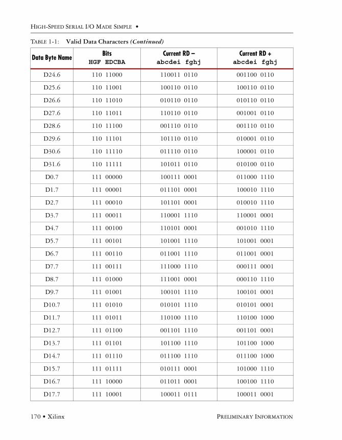
HIGH-SPEED SERIAL I/O MADE SIMPLE •
170 • Xilinx PRELIMINARY INFORMATION
D24.6 110 11000 110011 0110 001100 0110
D25.6 110 11001 100110 0110 100110 0110
D26.6 110 11010 010110 0110 010110 0110
D27.6 110 11011 110110 0110 001001 0110
D28.6 110 11100 001110 0110 001110 0110
D29.6 110 11101 101110 0110 010001 0110
D30.6 110 11110 011110 0110 100001 0110
D31.6 110 11111 101011 0110 010100 0110
D0.7 111 00000 100111 0001 011000 1110
D1.7 111 00001 011101 0001 100010 1110
D2.7 111 00010 101101 0001 010010 1110
D3.7 111 00011 110001 1110 110001 0001
D4.7 111 00100 110101 0001 001010 1110
D5.7 111 00101 101001 1110 101001 0001
D6.7 111 00110 011001 1110 011001 0001
D7.7 111 00111 111000 1110 000111 0001
D8.7 111 01000 111001 0001 000110 1110
D9.7 111 01001 100101 1110 100101 0001
D10.7 111 01010 010101 1110 010101 0001
D11.7 111 01011 110100 1110 110100 1000
D12.7 111 01100 001101 1110 001101 0001
D13.7 111 01101 101100 1110 101100 1000
D14.7 111 01110 011100 1110 011100 1000
D15.7 111 01111 010111 0001 101000 1110
D16.7 111 10000 011011 0001 100100 1110
D17.7 111 10001 100011 0111 100011 0001
TABLE 1-1: Valid Data Characters (Continued)
Data Byte Name Bits HGF EDCBA
Current RD –abcdei fghj
Current RD + abcdei fghj

8B/10B TABLES
PRELIMINARY INFORMATION XILINX • 171
D18.7 111 10010 010011 0111 010011 0001
D19.7 111 10011 110010 1110 110010 0001
D20.7 111 10100 001011 0111 001011 0001
D21.7 111 10101 101010 1110 101010 0001
D22.7 111 10110 011010 1110 011010 0001
D23.7 111 10111 111010 0001 000101 1110
D24.7 111 11000 110011 0001 001100 1110
D25.7 111 11001 100110 1110 100110 0001
D26.7 111 11010 010110 1110 010110 0001
D27.7 111 11011 110110 0001 001001 1110
D28.7 111 11100 001110 1110 001110 0001
D29.7 111 11101 101110 0001 010001 1110
D30.7 111 11110 011110 0001 100001 1110
D31.7 111 11111 101011 0001 010100 1110
TABLE 1-2: Valid Control “K” Characters
Special Code Name
Bits HGF EDCBA
Current RD –abcdei fghj
Current RD +abcdei fghj
K28.0 000 11100 001111 0100 110000 1011
K28.1 001 11100 001111 1001 110000 0110
K28.2 010 11100 001111 0101 110000 1010
K28.3 011 11100 001111 0011 110000 1100
K28.4 100 11100 001111 0010 110000 1101
K28.5 101 11100 001111 1010 110000 0101
K28.6 110 11100 001111 0110 110000 1001
K28.7(1) 111 11100 001111 1000 110000 0111
K23.7 111 10111 111010 1000 000101 0111
TABLE 1-1: Valid Data Characters (Continued)
Data Byte Name Bits HGF EDCBA
Current RD –abcdei fghj
Current RD + abcdei fghj

HIGH-SPEED SERIAL I/O MADE SIMPLE •
172 • Xilinx PRELIMINARY INFORMATION
K27.7 111 11011 110110 1000 001001 0111
K29.7 111 11101 101110 1000 010001 0111
K30.7 111 11110 011110 1000 100001 0111
Notes: 1. Used for testing and characterization only.
TABLE 1-2: Valid Control “K” Characters (Continued)
Special Code Name
Bits HGF EDCBA
Current RD –abcdei fghj
Current RD +abcdei fghj

PRELIMINARY INFORMATION XILINX • 173
APPENDIX C
A Comparison of Two Different
FPGA-to-FPGA Data Links
by Carl Christensen
Thomson Multimedia, November 6, 2002
AbstractThis paper is a detailed comparison of the design of two distinctly different FPGA-to-FPGA data links within the same system. It describes how a fast data link was implemented by using a Xilinx RocketIO™ SERDES running at 3.125 Gb/s with 8b10b encoding to achieve a 2.5 Gb/s payload between FPGAs in different chassis over multiple meters of cable. It also describes how a much slower data link was implemented within the same system by using a double data rate (DDR) LVDS with clock forwarding and at a clock rate of 156 MHz to achieve a 400 Mb/s payload between FPGAs in the same chassis, but on separate PCBs. The presentation touches on some key PCB/analog concerns, but mainly focuses on digital implementation, synthesis, simulation, interface, PAR, and timing con-straints.
When system development began, it seemed obvious to designers that the fast link would be dif-ficult to incorporate and the slow link would be simple. Although both links were successfully imple-mented in the design, the data link that was actually most difficult to incorporate was unexpected.
IntroductionAs we began to develop the architecture for a new product, we realized that we needed two distinctly different data links within our new product. The first data link requirement was for approximately 400 Mb/s, and the second required approximately 2.5 Gb/s. The slower link was to communicate between two FPGAs, each located on different PCBs but within the same chassis. The fast link was to also communicate between two FPGAs, but with each FPGA located in different chassis. As develop-ment began, it seemed obvious that the fast link would be difficult to incorporate, and the slow link would be simple.
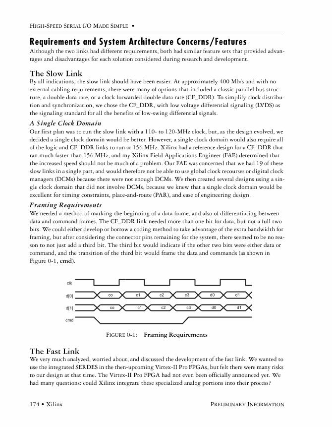
HIGH-SPEED SERIAL I/O MADE SIMPLE •
174 • Xilinx PRELIMINARY INFORMATION
Requirements and System Architecture Concerns/FeaturesAlthough the two links had different requirements, both had similar feature sets that provided advan-tages and disadvantages for each solution considered during research and development.
The Slow LinkBy all indications, the slow link should have been easier. At approximately 400 Mb/s and with no external cabling requirements, there were many of options that included a classic parallel bus struc-ture, a double data rate, or a clock forwarded double data rate (CF_DDR). To simplify clock distribu-tion and synchronization, we chose the CF_DDR, with low voltage differential signaling (LVDS) as the signaling standard for all the benefits of low-swing differential signals.
A Single Clock DomainOur first plan was to run the slow link with a 110- to 120-MHz clock, but, as the design evolved, we decided a single clock domain would be better. However, a single clock domain would also require all of the logic and CF_DDR links to run at 156 MHz. Xilinx had a reference design for a CF_DDR that ran much faster than 156 MHz, and my Xilinx Field Applications Engineer (FAE) determined that the increased speed should not be much of a problem. Our FAE was concerned that we had 19 of these slow links in a single part, and would therefore not be able to use global clock recourses or digital clock managers (DCMs) because there were not enough DCMs. We then created several designs using a sin-gle clock domain that did not involve DCMs, because we knew that a single clock domain would be excellent for timing constraints, place-and-route (PAR), and ease of engineering design.
Framing RequirementsWe needed a method of marking the beginning of a data frame, and also of differentiating between data and command frames. The CF_DDR link needed more than one bit for data, but not a full two bits. We could either develop or borrow a coding method to take advantage of the extra bandwidth for framing, but after considering the connector pins remaining for the system, there seemed to be no rea-son to not just add a third bit. The third bit would indicate if the other two bits were either data or command, and the transition of the third bit would frame the data and commands (as shown in Figure 0-1, cmd).
The Fast LinkWe very much analyzed, worried about, and discussed the development of the fast link. We wanted to use the integrated SERDES in the then-upcoming Virtex-II Pro FPGAs, but felt there were many risks to our design at that time. The Virtex-II Pro FPGA had not even been officially announced yet. We had many questions: could Xilinx integrate these specialized analog portions into their process?
FIGURE 0-1: Framing Requirements
clk
d[0]
d[1]
cmd
co c1 c2 c3 d0 d1
co c1 c2 c3 d0 d1

A COMPARISON OF TWO DIFFERENT FPGA-TO-FPGA DATA LINKS
PRELIMINARY INFORMATION XILINX • 175
Would the Virtex-II Pro be completed and released soon enough to be included in our product? In our research, we looked at several other options, including some networking- and fiber-based links. How-ever, all of our research kept pointing us back to a simple clock embedded link or SERDES with a sim-ple proprietary protocol.
Cost ConsiderationsUsing the Virtex-II Pro FPGA also helped with another requirement; low cost. While it was still too early for firm price quotes, the promise from Xilinx kept ringing in my head: “RocketIO™ and Pow-erPC™ for free.” I could use the Virtex-II Pro devices and have the integrated SERDES, or pay the same price for my programmable gates plus pay for the external SERDES. From a cost standpoint, the answer seemed obvious, but from a risk and scheduling standpoint, this option was not nearly as attractive. I thought perhaps we should just use an external SERDES. And, even if we did use the Mindspeed™ parts, maybe we could replace them later with Virtex-II Pro FPGAs.
Integrated SERDES vs. External SERDESAs we thoroughly investigated using an external SERDES, the Virtex-II Pro devices with the internal SERDES started looking more attractive because of both the I/O count and the simultaneous switch-ing outputs (SSO) involved. Our system needed to get 19 of the slower 400 Mb/s links and four of the fast links into and out of a single FPGA. Figure 0-2 illustrates our possible integrated SERDES approach, while Figure 0-3 illustrates an external SERDES approach.
FIGURE 0-2: Integrated SERDES
400 M
bit
400 M
bit
400 M
bit
400 M
bit
400 M
bit
3.135G
3.135G
3.135G
3.135G
3.135G
3.135G
3.135G
3.135G
400 M
bit
400 M
bit
400 M
bit
FPGA Significant Other IOClks, Strobes, and LEDs
19 Links Both
Directions
400 Mbit
152 Signals
16 Pins

HIGH-SPEED SERIAL I/O MADE SIMPLE •
176 • Xilinx PRELIMINARY INFORMATION
The Input/Output RequirementsThe I/O requirements for this design were becoming very extensive. If each slow link required four pair, that, in itself, was 152 pins, and we needed an additional 128 data lines plus control lines for the SERDES. The I/O requirement was now for over three hundred pins, and we had not even counted the remaining I/O connections like the clocks, resets, timing strobes, and LEDs. We started to determine bank assignments for different I/O standards, and it first appeared to us this approach was not going to work.
Simultaneous Switching OutputsBut there was an even bigger potential problem waiting just inside the proposed FPGA at the I/O ring. Xilinx (and all other FPGA manufacturers) make compromises when they design large FPGAs. One compromise was to not supply enough I/O ring power and ground connections to support using all of the I/O in a SSO environment. Aggravating this potential problem were some unique design-specific circumstances that further increased the challenge. The output streams (four 16-bit buses on most external SERDES) usually contained the same data. Thus, if one output was switching, there was a very high likelihood that four outputs were switching at the same time.
Framing RequirementsThe faster link also needed to be aligned, framed, and transitioned to ensure clock recovery. The obvi-ous choice was to use the 8b10b coding and decoding to guarantee adequate transitions for the embed-ded clock recovery and provide "k" characters for framing. The cost for all of this convenience was the need for an increase in the physical speed of the link from 2.5 Gb/s to 3.125 Gb/s. This could have been a problem. So, with all those benefits and the 8b10b encoders and decoders built into the multi-gigabit transcievers (MGTs), we investigated pushing 3.125 Gb/s across cable.
Cables, Boards, Backplanes, and ConnectorsI needed chassis-to-chassis communication over copper for at least 3 meters. Another interesting requirement was that the PCB the FPGA was to be mounted on must be hot swap replaceable from the front of the unit, and all interconnecting cables must enter on the back of the unit.
FIGURE 0-3: External SERDES
400 M
bit
400 M
bit
400 M
bit
400 M
bit
400 M
bit
3.135G
3.135G
3.135G
3.135G
3.135G
3.135G
3.135G
3.135G
400 M
bit
400 M
bit
400 M
bit
FPGASERDESSignificant Other IO
Clks, Strobes, and LEDs
19 Links Both
Directions
400 Mbit
152 Signals
128 Pins +
Clock and Control(256 Pins with some SERDES)
16 Pins
2.5G 16 Bi ts a t 156 MHz
2.5G 16 Bi ts a t 156 MHz
2.5G 16 Bi ts a t 156 MHz
2.5G 16 Bi ts a t 156 MHz
2.5G 16 Bi ts a t 156 MHz
2.5G 16 Bi ts a t 156 MHz
2.5G 16 Bi ts a t 156 MHz
2.5G 16 Bi ts a t 156 MHz

A COMPARISON OF TWO DIFFERENT FPGA-TO-FPGA DATA LINKS
PRELIMINARY INFORMATION XILINX • 177
Xilinx was at first unsure of this approach because they had only tested their FPGA over inches of FR4 PC boards with only two connectors. However, Xilinx also indicated that if I wanted to try a new implementation, they would like to observe the testing. Fortunately, I had a ready solution—some of the best high-speed signal manipulation engineers in the industry were working with me at that time, and were ready to design what I needed. They had years of experience pushing high definition serial digital video signal through connectors, backplanes, and cables. And while the bit rate of those signals was only 1.5 Gb/s, it had potential for long transitionless gaps. The spectrum was fondly referred to as "DC to light," and it is an unpleasant looking signal. I wanted faster speed and also the guaranteed transitions provided by 8b10b coding and decoding. My high-speed engineering experts were confi-dent we could get the cables and connectors to perform properly, but they were concerned about dig-ital noise getting into the analog circuitry. Fortunately, we decide to attempt this approach anyway.
Implementation DetailsThe architecture was finally in place and it was time to start writing Verilog HDL to implement our hardware design.
The Slow LinkCoding the CF_DDR links was not extremely difficult, but it was not as easy as we thought it would be either. We had planned on using a reference design from the Xilinx web site as a starting point, but the reference design used structural primitives rather than a behavioral approach. We do not like to instantiate primitives, and were assuming we could write Register Transfer Language (RTL) Verilog and feed it through the tools.
As we began the design, questions started to arise. How could we guarantee use of the DDR fea-tures of the Input/Output Block (IOB)? How did the LVDS I/O standard fit into all of this? Different synthesis tools changed the approaches slightly.
In the end, some instantiation of primitives was needed. The primitives that were instantiated rather than inferred in our design are listed in Table 1.
We soon had a design in place that was mostly RTL and had been verified through simulation. We also had investigated the synthesis results and verified that we were using the DDR feature of the IOBs. A quick operation of one receiver and one transmitter showed that the 156-MHz clock rate was easy to incorporate as well. We thought the design was complete, and we published it internal to the company so it could be used by the various designs that would need it.
The Fast LinkWe were not certain what to expect when coding the MGTs in our design. When we began the design, the MGT product had not been officially announced and operational data was not available. The only information we really had to base expectations on was a Mindspeed data sheet. But once we learned
TABLE C-1: Instantiated Primitives
RAM16X1D
FDDRRSE
IBUFDS
OBUFDS

HIGH-SPEED SERIAL I/O MADE SIMPLE •
178 • Xilinx PRELIMINARY INFORMATION
that Xilinx had incorporated a new digital interface to the Mindspeed core, all we could do was wait for our early access data. Finally, I received a telephone call from my Xilinx representative. Xilinx had some data for me, but I needed to prepare myself because it was a lot of data. I already knew that the PowerPC would be complicated and that it would have a lot of documentation, so I reminded him that I was not using the CPU core. He smiled and replied that the MGT portion of the documentation data set, alone, was over 1000 pages! As I hung up the telephone, I began to realized the huge task we were facing with the MGT portion of our design. The MGT was a complex core and we needed to under-stand it. I knew I must find a knowledgeable design person to dedicate full-time to the MGTs.
Developing the code itself was quite easy. We just cut and pasted some sample instances, then modified them to fit our design needs. It was more difficult, however, to know how to set the many parameters and setup ports, but not as difficult as I had first imagined. This task would have been even easier if we were planning to use one of the pre-defined standards such as XAUI. Xilinx had all of the parameters for the pre-defined standards already set up, but our custom application required a little more effort.
Simulation also required a few changes. The models of the MGT were SWIFT or encrypted mod-els. But after an upgrade to Model Sim SE and a few modifications to the scripts supplied as part of the MGT development kit, we were simulating our 3 Gb/s link.
Proving Our ConceptWith so much at risk, we decided to build a proof-of-concept board to characterize and qualify the approach. As almost an afterthought, we decided build a prototype of the slower link as well.
As the proof-of-concept boards neared completion, we received word that Xilinx would not be able to ship the Virtex-II Pro devices to us as early as we had expected. We decided to build some of the boards anyway to test other high-risk circuits. Once we had the boards in-house, we decided to also test the slower CF_DDR links. The data link we assumed would be simple to engineer suddenly became difficult.
Testing the Slow LinkOur use of the tools for speed verification had been hurried, and we discovered that the results were flawed. We had used only a simple period constraint with no offsets and no special consideration for the half-cycle paths, and assumed that the period constraint would mitigate any half-cycle concerns, but it had not. The prototype link was not working; not at 156 MHz and not at 96 MHz. The closer we looked; the more difficult this problem became.
Trying to test a few of these links in an otherwise empty part was agonizing. The placer was plac-ing the logic everywhere and anywhere. As we got into the details of the reference design, we discov-ered I/O tiles. Because they were so poorly documented, it was difficult to determine how they functioned. We also struggled to find the right way to help the placer through timing constraints. This was supposed to be easy, yet, it became painfully difficult.
Input/Output Tiles and Pin PlacementAs the mystery of the I/O tiles began to unfold, we could see that the advertised fast DDR rates were reachable, but only as an isolated, hand crafted solution. Such links would not operate as fast through our normal design methodologies (RTL with timing driven PAR, and I/O placement picked for ease of board routing).

A COMPARISON OF TWO DIFFERENT FPGA-TO-FPGA DATA LINKS
PRELIMINARY INFORMATION XILINX • 179
Input/Output tiles were made up of certain groups of four adjacent IOBs with some special extra-fast interconnect. The I/O tiles only exist on the two "vertical" sides of the die, and they only come in groups of four. In past years we would always pick the pins based on logic/data flow. But as the pin counts and routing resources increased, it had became common practice for us to let the PCB designer pick pins. Figure 1-1 is an example of the pins selected by logic/data flow. Figure 1-2 is an example of pin selection when the PCB designer picked the pins.
This normally is not a very involved process, but if we wanted to be in the same IO tile, we had to be in adjacent IOBs. Luckily, some of our I/O was on adjacent IOBs on the vertical sides. This did not help much because, even though we had only four signals (three data and a clock), we were using LVDS. With differential signaling we could only get two signals per tile. Then we worried: what if two of our signals were in the same tile and two were not, was the skew worse than if they had all been in separate tiles? Finally, we ignored I/O tiles, but picked adjacent IOBs to improve local clock rout-ing.
FIGURE 1-1: Pins Selected Based on Logic/Data Flow
FIGURE 1-2: Pins Selected by PCB Designer

HIGH-SPEED SERIAL I/O MADE SIMPLE •
180 • Xilinx PRELIMINARY INFORMATION
Local ClockingWe could not use global clocking resources, global buffering (BUFG), or DCM for the forwarded clock that came with the data because we needed 19 slow links in a single FPGA. This local clock routing was actually the cause of the prototype failures.
We did not have much logic in the parts other than the CF_DDR links and associated test cir-cuitry, but, the placer tried to spread the logic over the entire chip. Once we started to get placements that were reasonable, it then became obvious that merely controlling the placement would not be enough. We needed to change the structure of the logic, as shown the simplified block diagram in Figure 1-3.
The Arbuckle MethodThere is a subtle trick hidden in the structure of the CF_DDR_RX. We fondly refer to it as the Arbuckle method after the designer who originated it in a Xilinx design that has more clock domains than global clock buffers. The problem with local clocks is skew. Without the global clock buffers, it
FIGURE 1-3: New Structure Block Diagram
cf_clk
bufg
cf_data0
cf_data1
DPRAMD_IN
IN_ADDROUT_ADDR
CounterCounter
D_OUT
cf_cmd
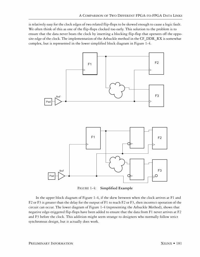
A COMPARISON OF TWO DIFFERENT FPGA-TO-FPGA DATA LINKS
PRELIMINARY INFORMATION XILINX • 181
is relatively easy for the clock edges of two related flip-flops to be skewed enough to cause a logic fault. We often think of this as one of the flip-flops clocked too early. This solution to the problem is to ensure that the data never beats the clock by inserting a blocking flip-flop that operates off the oppo-site edge of the clock. The implementation of the Arbuckle method in the CF_DDR_RX is somewhat complex, but is represented in the lower simplified block diagram in Figure 1-4.
In the upper block diagram of Figure 1-4, if the skew between when the clock arrives at F1 and F2 or F3 is greater than the delay for the output of F1 to reach F2 or F3, then incorrect operation of the circuit can occur. The lower diagram of Figure 1-4 (representing the Arbuckle Method), shows that negative edge-triggered flip-flops have been added to ensure that the data from F1 never arrives at F2 and F3 before the clock. This addition might seem strange to designers who normally follow strict synchronous design, but it actually does work.
FIGURE 1-4: Simplified Example
F1
F3
F2
F2
F3
Pad
ibuf
Pad
F1
ibuf
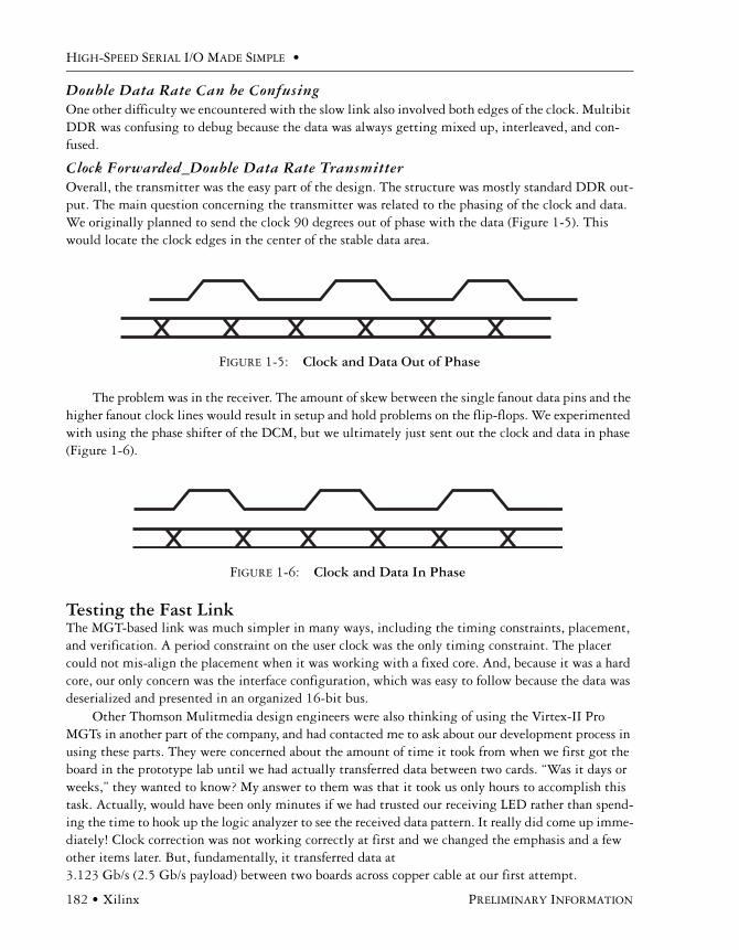
HIGH-SPEED SERIAL I/O MADE SIMPLE •
182 • Xilinx PRELIMINARY INFORMATION
Double Data Rate Can be ConfusingOne other difficulty we encountered with the slow link also involved both edges of the clock. Multibit DDR was confusing to debug because the data was always getting mixed up, interleaved, and con-fused.
Clock Forwarded_Double Data Rate Transmitter Overall, the transmitter was the easy part of the design. The structure was mostly standard DDR out-put. The main question concerning the transmitter was related to the phasing of the clock and data. We originally planned to send the clock 90 degrees out of phase with the data (Figure 1-5). This would locate the clock edges in the center of the stable data area.
The problem was in the receiver. The amount of skew between the single fanout data pins and the higher fanout clock lines would result in setup and hold problems on the flip-flops. We experimented with using the phase shifter of the DCM, but we ultimately just sent out the clock and data in phase (Figure 1-6).
Testing the Fast LinkThe MGT-based link was much simpler in many ways, including the timing constraints, placement, and verification. A period constraint on the user clock was the only timing constraint. The placer could not mis-align the placement when it was working with a fixed core. And, because it was a hard core, our only concern was the interface configuration, which was easy to follow because the data was deserialized and presented in an organized 16-bit bus.
Other Thomson Mulitmedia design engineers were also thinking of using the Virtex-II Pro MGTs in another part of the company, and had contacted me to ask about our development process in using these parts. They were concerned about the amount of time it took from when we first got the board in the prototype lab until we had actually transferred data between two cards. “Was it days or weeks,” they wanted to know? My answer to them was that it took us only hours to accomplish this task. Actually, would have been only minutes if we had trusted our receiving LED rather than spend-ing the time to hook up the logic analyzer to see the received data pattern. It really did come up imme-diately! Clock correction was not working correctly at first and we changed the emphasis and a few other items later. But, fundamentally, it transferred data at 3.123 Gb/s (2.5 Gb/s payload) between two boards across copper cable at our first attempt.
FIGURE 1-5: Clock and Data Out of Phase
FIGURE 1-6: Clock and Data In Phase
A COMPARISON OF TWO DIFFERENT FPGA-TO-FPGA DATA LINKS
PRELIMINARY INFORMATION XILINX • 183
Fast Link Problems and SolutionsI am not saying that the MGT design was painless. There were tool problems, documentation prob-lems, and other surprises. But, because we had expected some problems, we were able to adapt early in the process.
Differential BREF Clock PinsThe first big surprise put the finished board design on hold just prior to ordering the raw boards. My Xilinx FAE telephoned me to tell me that if I wanted to run at 3.2 Gb/s, we needed to be on special clock pins. Evidently, there were special low-skew clock lines (BREFCLK) that went directly to the MGT. Our problem was that no one knew exactly which pins were the BREF clock these pins. Our board design was on hold for two days as we worked to track down the mysterious BREF clock pins.
We finally determined the BREF pin numbers, but that was not the end of our BREF problems. The BREF pins were difficult to identify because Xilinx had hoped that the pins would not be needed. In fact, support for the BREF paths had been eliminated from the first version of the Virtex-II Pro FPGA support tools. Fortunately, there was a patch, but the patch turned out to be different from most EDA patches. Besides a script that was run once, there were a series of mouse movements and clicks in FPGA editor that had to be repeated each and every time we went through PAR. This all eventually worked out, but we did have some frustrating moments.
Confusing DocumentationDocumentation that was confusing originally caused us some frustration. However, most of the con-fusion was related to clock correction and other comma/"k" character issues. Many of these issues were not mistakes, but, rather, confusing wording that has since been revised.
Managing ParametersOne other unpleasant aspect of the MGT is managing the parameters in Verilog. With 46 parameters to set, it was certain to be a large effort. But with different synthesis tools and simulation needing dif-ferent syntax, the potential for simulation and the lab getting out of sync was certainly there. We never actually had a problem, most likely because we were so worried about it.
Maybe these large primitives will be what it takes to get rid of all these comments that are not comments, and have all tools support parameters as defined in the language. Below is an example of the syntax for two of the four tools. Note that the first syntax must be one line of text.
/* synthesis xc_props = "ALIGN_COMMA_MSB=TRUE, CHAN_BOND_MODE=OFF, CHAN_BOND_OFFSET=0000, CHAN_BOND_ONE_SHOT=FALSE, CHAN_BOND_SEQ_1_1=10001000001, CHAN_BOND_SEQ_1_2=10001000010, CHAN_BOND_SEQ_1_3=10001000011, CHAN_BOND_SEQ_1_4=10001000100, CHAN_BOND_SEQ_2_1=10001001001, CHAN_BOND_SEQ_2_2=10001001010, CHAN_BOND_SEQ_2_3=10001001011, CHAN_BOND_SEQ_2_4=10001001100, CHAN_BOND_SEQ_2_USE=FALSE, CHAN_BOND_SEQ_LEN=2, CHAN_BOND_WAIT=5, CLK_CORRECT_USE=TRUE, CLK_COR_INSERT_IDLE_FLAG=FALSE, CLK_COR_KEEP_IDLE=FALSE, CLK_COR_REPEAT_WAIT=00000, CLK_COR_SEQ_1_1=00110111100, CLK_COR_SEQ_1_2=00010010101, CLK_COR_SEQ_1_3=00010111100, CLK_COR_SEQ_1_4=00010110101, CLK_COR_SEQ_2_1=10010001001, CLK_COR_SEQ_2_2=10010001010, CLK_COR_SEQ_2_3=10010001011, CLK_COR_SEQ_2_4=10010001100, CLK_COR_SEQ_2_USE=FALSE, CLK_COR_SEQ_LEN=4, COMMA_10B_MASK=1111111000, DEC_MCOMMA_DETECT=TRUE, DEC_PCOMMA_DETECT=TRUE, DEC_VALID_COMMA_ONLY=FALSE, MCOMMA_10B_VALUE=1100000000, MCOMMA_DETECT=FALSE, PCOMMA_10B_VALUE=0

HIGH-SPEED SERIAL I/O MADE SIMPLE •
184 • Xilinx PRELIMINARY INFORMATION
11111000, PCOMMA_DETECT=TRUE, RX_BUFFER_SE=TRUE, RX_DATA_WIDTH=2, RX_DECODE_USE=TRUE, RX_LOSS_OF_SYNC_FSM=FALSE, TERMINATION_IMP=50, SERDES_10B=FALSE, TX_BUFFER_USE=TRUE, TX_DATA_WIDTH=2, TX_DIFF_CTRL=400, TX_PREEMPHASIS=3" */;
// XST Primitive Attributes// synthesis attribute ALIGN_COMMA_MSB of gb_transceiver_m is "TRUE"// synthesis attribute CHAN_BOND_MODE of gb_transceiver_m is "OFF"// synthesis attribute CHAN_BOND_OFFSET of gb_transceiver_m is "0000"// synthesis attribute CHAN_BOND_ONE_SHOT of gb_transceiver_m is "FALSE"// synthesis attribute CHAN_BOND_SEQ_1_1 of gb_transceiver_m is "10001000001"// synthesis attribute CHAN_BOND_SEQ_1_2 of gb_transceiver_m is "10001000010"// synthesis attribute CHAN_BOND_SEQ_1_3 of gb_transceiver_m is "10001000011"// synthesis attribute CHAN_BOND_SEQ_1_4 of gb_transceiver_m is "10001000100"// synthesis attribute CHAN_BOND_SEQ_2_1 of gb_transceiver_m is "10001001001"// synthesis attribute CHAN_BOND_SEQ_2_2 of gb_transceiver_m is "10001001010"// synthesis attribute CHAN_BOND_SEQ_2_3 of gb_transceiver_m is "10001001011"// synthesis attribute CHAN_BOND_SEQ_2_4 of gb_transceiver_m is "10001001100"// synthesis attribute CHAN_BOND_SEQ_2_USE of gb_transceiver_m is "FALSE"// synthesis attribute CHAN_BOND_SEQ_LEN of gb_transceiver_m is "2"// synthesis attribute CHAN_BOND_WAIT of gb_transceiver_m is "5"// synthesis attribute CLK_COR_INSERT_IDLE_FLAG of gb_transceiver_m is "FALSE"// synthesis attribute CLK_COR_KEEP_IDLE of gb_transceiver_m is "FALSE"// synthesis attribute CLK_COR_REPEAT_WAIT of gb_transceiver_m is "00000"// synthesis attribute CLK_COR_SEQ_1_1 of gb_transceiver_m is "00110111100" // synthesis attribute CLK_COR_SEQ_1_2 of gb_transceiver_m is "00010010101" // synthesis attribute CLK_COR_SEQ_1_3 of gb_transceiver_m is "00010111100" // synthesis attribute CLK_COR_SEQ_1_4 of gb_transceiver_m is "00010110101"
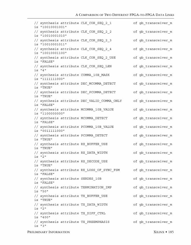
A COMPARISON OF TWO DIFFERENT FPGA-TO-FPGA DATA LINKS
PRELIMINARY INFORMATION XILINX • 185
// synthesis attribute CLK_COR_SEQ_2_1 of gb_transceiver_m is "10010001001"
// synthesis attribute CLK_COR_SEQ_2_2 of gb_transceiver_m is "10010001010"
// synthesis attribute CLK_COR_SEQ_2_3 of gb_transceiver_m is "10010001011"
// synthesis attribute CLK_COR_SEQ_2_4 of gb_transceiver_m is "10010001100"
// synthesis attribute CLK_COR_SEQ_2_USE of gb_transceiver_m is "FALSE"
// synthesis attribute CLK_COR_SEQ_LEN of gb_transceiver_m is "4"
// synthesis attribute COMMA_10B_MASK of gb_transceiver_m is "1111111000"
// synthesis attribute DEC_MCOMMA_DETECT of gb_transceiver_m is "TRUE"
// synthesis attribute DEC_PCOMMA_DETECT of gb_transceiver_m is "TRUE"
// synthesis attribute DEC_VALID_COMMA_ONLY of gb_transceiver_m is "FALSE"
// synthesis attribute MCOMMA_10B_VALUE of gb_transceiver_m is "1100000000"
// synthesis attribute MCOMMA_DETECT of gb_transceiver_m is "FALSE"
// synthesis attribute PCOMMA_10B_VALUE of gb_transceiver_m is "0011111000"
// synthesis attribute PCOMMA_DETECT of gb_transceiver_m is "TRUE"
// synthesis attribute RX_BUFFER_USE of gb_transceiver_m is "TRUE"
// synthesis attribute RX_DATA_WIDTH of gb_transceiver_m is "2"
// synthesis attribute RX_DECODE_USE of gb_transceiver_m is "TRUE"
// synthesis attribute RX_LOSS_OF_SYNC_FSM of gb_transceiver_m is "FALSE"
// synthesis attribute SERDES_10B of gb_transceiver_m is "FALSE"
// synthesis attribute TERMINATION_IMP of gb_transceiver_m is "50"
// synthesis attribute TX_BUFFER_USE of gb_transceiver_m is "TRUE"
// synthesis attribute TX_DATA_WIDTH of gb_transceiver_m is "2"
// synthesis attribute TX_DIFF_CTRL of gb_transceiver_m is "400"
// synthesis attribute TX_PREEMPHASIS of gb_transceiver_m is "3"
HIGH-SPEED SERIAL I/O MADE SIMPLE •
186 • Xilinx PRELIMINARY INFORMATION
More Difficult Board DesignAnother challenge for the MGT-based link included a board design that was more difficult than antic-ipated. Board impedances needed to be carefully controlled. Stubs, including stubs created when via-ing to a different layer, and special requirements pertaining to power supplies and bypassing were all new to me as an FPGA person. But my high-speed experts knew just what to do.
ConclusionThe initial estimates were that the MGT-based link would be on order of magnitude more difficult than the slower clock forwarded design. They turned out to be approximately the same amount of work.
Multibit DDR with clock forwarding provides a reasonable way to move data between two FPGAs at moderate rates, and also in circumstances where global clocking resources can be used for the forwarded clocks. To push the speed or avoid using global clocking, some extra work might be required.
But, with fewer pins, more speed, and all the other benefits, an integrated SERDES is a better solution. We will use the MGT links again and encourage Xilinx to give us both faster and slower SERDES in the future.
AcknowledgementsI would like to acknowledge Lynn Arbuckle, Dave Bytheway, and Randall Redondo of Thomson, who did most of the real work discussed in this paper. Barry Albright and Marc Walker are the high-speed experts, also of Thomson. I would also like to acknowledge the outstanding support provided by Jeff Hutchings, my Xilinx FAE, and Tim Hemphill, my Xilinx sales representative. And finally, thank you to my technical editor, Sandy Christensen, who is also my loving and supportive wife.
GLOSSARY
PRELIMINARY INFORMATION XILINX • 187
APPENDIX D
Glossary
4b/5b: Similar to 8b/10b encoder, but simpler. As the name implies, 4 bits are encoded into 5 bits. The 4b/5b advantage over 8b/10b is that its encoders and decoders are much simpler. The downside is that there are few control characters and it does not handle the DC balance or disparity problem. With the same coding overhead and less functionality, 4b/5b is not often used anymore.
64b/66b: A line encoding scheme developed for 10-Gigabit Ethernet that uses a scrambling method combined with a non-scrambled sync pattern and control type.
8b/10b: An encoding scheme developed by IBM that has been widely adapted. It is a value lookup-type encoding scheme where 8-bit words are translated into 10-bit symbols. These symbols ensure a good number of transitions for the clock recovery.
AC Coupling: Method of connecting a receiver to a transmitter through series capacitors. Allows for dc biases differences between the receiver and transmitter.
Active Equalizer: Can be thought of as a frequency dependant amplifier/attenuator.
Addressing/switching/forwarding: While the direct point-to-point nature of a serial protocol elim-inates many of the needs for an addressing scheme, some of the more complex protocols include addressing schemes. With addressing comes the possibility for forwarding and switching.
Advanced Switching: A switched fabric protocol built on the same physical and data level protocol as PCI Express. An emerging standard set to be a significant player in the switched fabric arena.
Alignment Sequence: A unique bit pattern in the serial stream that can be used to determine word/symbol alignment. Often consist of a pair of reserved symbols that form a unique bit sequence that is impossible to generate elsewhere in the stream.
ASIC: Application Specific Integrated Circuit.
ASSP: Application Specific Standard Part.
ATCA: Advanced Telecom Computing Architecture or AdvancedTCA, this PICMG spec standard is a specification for next generation telecommunication cabinets. Its aim is to ease multi-vendor interoperability while providing a very flexible, very scalable system. The standard has various imple-mentations within a common theme. Architectures for star-based backplanes, redundant star-based backplanes, and fully connected mesh are included.
Aurora: A relatively simple protocol that handles only link-layer and physical issues.
Back drilling: After plating, the unused portion of the via is removed by drilling.
Backplane: A common bus at the rear of the computer chassis connecting each circuit card slot to the other parts of the system, such as the motherboard on a PC. It also distributes low-voltage AC and DC, filtered and un-filtered power to each slot. As a rigid circuit board, a backplane can support higher connection speeds and more logic. They are used in large-scale network switches and routers.
HIGH-SPEED SERIAL I/O MADE SIMPLE •
188 • Xilinx PRELIMINARY INFORMATION
BERS: Bit Error Rates.
BGA: Ball Grid Array. (Sometimes abbreviated BG.) As opposed to a pin grid array (PGA), a ball grid array is a type of microchip connection methodology. Ball grid array chips typically use a group of sol-der dots, or balls, arranged in concentric rectangles to connect to a circuit board.
Bridge: A device that forwards traffic between network segments based on (OSI Reference Model) data link layer information. These segments would have a common network layer address. A bridge can connect different kinds of networks (e.g., wireless LAN to Ethernet).
BUFG: Global buffer.
Cat 5: A grade of twisted pair wiring commonly installed in office buildings.
Channel Bonding: Channel bonding absorbs the skew between two or more MGTs, and presents the data to the user as if it were transmitted over a single link.
CLK: Clock. A circuit in a computer that uses a quartz crystal to generate a series of regular pulses that are sent to the CPU. The clock is the heartbeat of the computer. Switching operations in the computer take place while the clock is sending a pulse. The faster the clock speed, the more instructions per sec-ond the computer can execute.
Clock Correction and Channel Bonding: Allows for correction of a difference between the transmit clock and the receive clock. Also allows for skew correction between multiple channels. (Channel bonding is optional and not always included in SERDES.)
Clock Domains: Logic clocked by the same clock source are said to be in the same clock domain.
Clock Forwarded: Clock forwarded (cf) or forwarding is another common term for source synchro-nous.
Clock Manager: Manages various clocking needs including clock multiplication, clock division, and clock recovery.
Clock Recovery: When a clock is derived from the transitions of the incoming bit stream.
Clock Tree: Traces and drivers in an IC that is designed to distribute a clock to the logic within given skew specification.
CML: Current Mode Logic; a differential based electrical interface well suited to the gigabit link.
CMOS: Complementary Metal Oxide Semiconductor.
Comma: One or two symbols specified to be the alignment sequence. This sequence can usually be set in the transceiver, but in some cases it may be predefined.
Cosmic Rays: A generic term often used to describe any of several types of high energy electromag-netic radiation, including gamma rays and alpha and beta particle radiation.
CRC: Cyclic Redundancy Check; a method of determining errors in the transmission of data.
Cross-talk: Degrading of a signal as a result of the interference of another signal.
CSMA/CD: Carrier Sense Multiple Access with Collision Detection.
Data formats: Data value definitions for video and audio protocols; how we use the ones and zeros to represent specific values or meanings.
Datagram: A data packet carrying its own address information so it can be independently routed from its source to the destination computer.
GLOSSARY
PRELIMINARY INFORMATION XILINX • 189
Data striping: A common function of a protocol is to define of how and where data is separated from the overhead. This is commonly referred to as stripping or de-embedding.
DCA: Digital Communication Analyzer; takes the sampling scope and adds many of other features.
DC Balance: Average DC voltage of a bitstream. If the bitstream has more “ones” than “zeros,” it will have a positive DC balance. Normally, the ideal is to have a zero DC balance (the same number of “ones” and “zeros”).
DC Bias: A set DC voltage around which a transmitter or receiver operates.
DC Coupling: Method of connecting a receiver to a transmitter through direct connection, rather than through series capacitors used in AC coupling. The DC biases of the receiver and transmitter must be identical.
DCM: Digital Clock Manager.
DDR: Double Data Rate (in reference to RAM and registers).
De-emphasis: Overdriving the first of each transition or underdriving any consecutive bit times of the same value. (A different name for pre-emphasis.)
Deserializer: Takes a serial stream at a rate of n times y and changes it into parallel data of width n changing at rate y.
Deterministic jitter: The component of the jitter attributable to specific patterns or events. Includes jitter resulting from sources such as asymmetric rise/fall times, inter-symbol interference, power-sup-ply feed through, oscillator wand, and cross-talk from other signals. Often abbreviated as DJ or dj.
Digital Communication Analyzers: DCA — a sampling oscilloscope with additional features useful for analyzing data communication signals.
Digital Storage Scope: Converts the incoming signal to digital samples that are stored and then used to recreate the signal on an oscilloscope display.
Differential Signals: Signals that use both a positive and a negative line pair. The value of the signal is determined by the difference in voltage between the two signals of the pair. Differential signals are more robust than non-differential or single-ended signals.
DLL: Delay-Locked Loop (also known as digital delay-locked loops)
Dropped: Data is “dropped” when a FIFO storage register is getting close to full and does not write the incoming data sequence into storage at the next clock correction sequence.
DSP: (1) Digital Signal Processing. Using computers to process signals such as sound, video, and other analog signals that have been converted to digital form. Some uses of DSP are: to decode modu-lated signals from modems, to process sound, video, and images in various ways, and to understand data from sonar, radar, and seismological readings. (2) Digital Signal Processor. A specialized CPU used for digital signal processing. Some uses of digital signal processors are with modems and sound boards.
EDIF: Electronic Design Interchange Format
ef: End of frame.
EISA: Bus architecture used in early PCs.
Embedding: A protocol often defines how and where the data is embedded into the protocol streams or packets. This is especially true of protocols that follow the protocol stack model.
HIGH-SPEED SERIAL I/O MADE SIMPLE •
190 • Xilinx PRELIMINARY INFORMATION
EMI: ElectroMagnetic Immersions. Radiated electromagnetic energy is often subject to emissions standards set by government and standards agencies.
ESR: Effective Series Resistance. The undesirable, yet real, resistance quality of a capacitor.
ESL: Effective Series Inductance. The undesirable, yet real, inductive quality of a capacitor.
Ethernet: A common LAN protocol.
Eye pattern: The pattern formed when a sequence of snapshots of a waveform of random bits and of the same waveform duration are superimposed on one another.
FEC: Forward Error Correction <algorithm>. A class of methods for controlling errors in a one-way communication system. Forward Error Correction sends extra information along with the data, which can be used by the receiver to check and correct the data.
Ferrite Bead: An inductor made of a bead of ferrite material commonly used to suppress or filter energy of a certain frequency range.
FiberChannel: FiberChannel has always been a serial standard, but its speeds have increased over the years. As copper interconnects have advanced, it has also become available on copper as well as fiber optics.
Field solver: A tool/mathematical model that can determine the exact dimensions for any given impedance.
FIFO: First-in, first-out (as opposed to LIFO – last-in, first-out). A data structure or hardware buffer where items come out in the same order they came in.
FireWire: The former name for High-Performance Serial Bus. A serial bus developed by Apple Com-puter and Texas Instruments (IEEE 1394). The High Performance Serial Bus can connect up to 63 devices in a tree-like daisy chain configuration, and transmit data at up to 400 megabits per second. It supports plug-and-play and peer-to-peer communication.
Flip-chip: A surface mount chip technology where the chip is packaged in-place on the board and then under-filled with an epoxy. A common technique for attachment is to place solder balls on the chip, “flip” the chip over onto the board and melt the solder.
Flow control: Protocols can also define flow control. This can vary from defining a way of dynami-cally scaling sub-channel bandwidth allocation, to varying the ideal insertion rate to match the clock correction needs.
Fmax: Maximum toggle rate of a flip-flop in a given technology or part.
FOLS: Fiber Optic LAN Section (Telecommunications Industry Association).
FR-4: A common PCB assembly material.
Fractional Phase Detector: A phase detector that uses multiple phases of the same clock in the phase detection.
HSTL: High-Speed Transistor Logic.
IBIS models: text-based description of a circuit's behavior. Adequately accurate at frequencies below 1 GHz. Does not reveal construction details of the circuit.
IC Geometry: A way of grouping ICs by the size or dimension of the polygons. Examples include 0.25 micron and 90 nanometer.
Idle symbol or sequence: Symbol sent when there is no data to send.
GLOSSARY
PRELIMINARY INFORMATION XILINX • 191
IEEE 1394 FireWire™: A high performance serial bus for plug-and-play and peer-to-peer networks.
Infiniband: A box-to-box protocol run over either copper or fiber. Infiniband-style cables have become highly popular for multi-gigabit links of a few meters range. The specification allows for a variety of devices and complexity and includes specifications for repeaters, and switches or hubs to expand the number of connected devices.
ILD: Injection Laser Diode.
Impedance: The combined effect of capacitance, inductance, and resistance on a signal. According to Ohm’s law, voltage is the product of current and resistance at a given frequency.
Impedance is a measure of resistance to electrical current flow when a voltage is moved across it. Impedance is measured in ohms and is the ratio of voltage to the flow of current allowed.
Instantiate/instantiation: In programming, to produce a more defined version of an object by replac-ing variables with values (or other variables). As used in logic programming, this means to bind a logic variable (type variable) to some value (type).
IP: Intellectual Property (as in IP core).
ISA: A very early PC bus architecture.
ISI: Inter-symbol interference; happens when the serial stream contains a number of bit times of the same value followed by short bit times of the opposite value.
Isochronous: Matched in frequency but not necessarily matched in phase.
Jitter: Variation of the transition from the ideal transition placement; the difference between the ideal zero crossing and the actual zero crossing.
LFSR: Linear Feedback Shift Register.
Line Decoder: Decodes from line encoded data to plain data. (This is an optional block that is some-times done outside of the SERDES.)
Line Encoder: Encodes the data into a more line friendly format. This usually involves eliminating long sequences of non-changing bits. May also adjust data for even balance of ones and zeros. (This is an optional block sometimes not included in a SERDES.)
Line Encoding Schemes: A method of encoding data for transmission over a serial stream.
LVCMOS: Low Voltage Complementary Metal Oxide Semiconductor.
LVDS: Low Voltage Differential Signaling.
LVTTL: Low Voltage Transistor-Transistor Logic.
Packet: A well-defined collection of bytes, consisting of a header, data, and trailer.
Passive equalizer: A passive circuit that has a frequency response that is complementary to the trans-mission losses, similar to a filter.
MAC (Media Access Control): The lower sublayer of the OSI data link layer. The interface between a node's Logical Link Control and the network's physical layer. The MAC differs for various physical media.
Microstrip: A thin, strip-like transmission line used for transmitting microwave frequencies; typi-cally mounted on a flat dielectric substrate that is mounted on a ground plane.
MII: Media Independent Interface.

HIGH-SPEED SERIAL I/O MADE SIMPLE •
192 • Xilinx PRELIMINARY INFORMATION
MSB: Most Significant Bit. In a binary number, this is the bit that is the farthest to the left, and has the greatest weight.
OC: Optical Carrier. The transmission speeds defined in the SONET specification. Optical Carrier defines transmission by optical devices, and STS is the electrical equivalent.
OC-192: Optical Carrier 192 (10 Gb/s).
PAR: Place-and-route.
PCB Assemblies: Assembled circuit boards.
PCI: Peripheral Component Interconnect. A personal computer local bus designed by Intel that oper-ates at 33 MHz and supports Plug and Play. It provides a high-speed connection with peripherals and allows connection of seven peripheral devices. It is mostly used with Pentium computers, but is pro-cessor independent and therefore able to work with other processors. It plugs into a PCI slot on the motherboard and can be used along with an ISA or EISA bus.
PCI Express: Takes the old parallel PCI structure and updates it to a high-speed serial structure. Upper levels of the protocol remain compatible providing an easy adaptation into legacy PCI systems.
PCMCIA: A bus architecture commonly used in notebook computers.
Physical interface: Drive levels, pre-emphasis, etc., are specified by the protocol to ensure compati-bility between devices.
Physical layer interface: The portion of a protocol dealing with the physical/electrical characteristics of the signals. Also called a PHY.
PICMG: PICMG is a consortium of over 600 companies who collaboratively develop open specifica-tions for high performance standardized backplane architectures. Many of these standards use other industry standards such as PCI and Infiniband.
PLL: Phased-Locked Loop. A circuit that takes a reference clock and an incoming signal and creates a new clock that is locked to the incoming signal.
Power Integrity Tools: These tools help design the power delivery (bypassing, filtering, etc.) system. Many are add-on to signal integrity analysis tools. These tools provide the same type of functionality for power systems as the SI tools do for signals.
ppm: Parts per million; a way of describing a very small ratio.
Pre-emphasis: Intentional overdriving at the first of a transition.
Principle of total internal reflection: When the angle of incidence exceeds a critical value, light cannot get out of the glass. Instead, the light bounces back in.
Random jitter: The component of the jitter resulting from differential and common mode stochastic noise processes such as power supply noise and thermal noise. Also known as rj, RJ, and called inde-terministic jitter.
Receive FIFO: Allows for storing of received data before removal; is essential in system where clock correction is required.
Receive Line Interface: Analog receive circuitry includes differential receiver and may include active or passive equalization.
Reed-Soloman: A popular and powerful forward error correction method.

GLOSSARY
PRELIMINARY INFORMATION XILINX • 193
Repeating: If the FIFO is getting close to empty, the next time a clock correction sequence is found it will be written into the FIFO twice.
Rise time: The time it takes a signal to transition from a zero to a one.
ROGERS 3450: A material used for assembling circuit boards or PCBs. This particular material has less loss at high frequencies than most materials.
RS-232: Recommended Standard 232. This is the de facto standard for communication through PC serial ports. It can refer to cables and ports that support the RS-232 standard.
RTL: Register Transfer Level/Language (software). A kind of hardware description language (HDL) used in describing the registers of a computer or digital electronic system, and the way in which data is transferred between them. An intermediate code for a machine with an infinite number of registers.
S-parameter: Text-based description of the behavior of a circuit, board traces, or connectors at very high frequencies. Originally used in microwave design, s-parameters are now being used to more effi-ciently model high-speed board and connector assemblies. S-parameters describe the scattering and reflection of traveling waves in a transmission line.
Sampling scope: An oscilloscope that digitizes information and stores it. To capture signals faster than the analog-to-digital converters can go, the scope captures only a few samples of each period. Moving the sampling each time allows it to capture enough signals to represent a repetitive signal.
Scrambling: A way of reordering or encoding the data so that it appears to be random, but it can be unscrambled.
SCSI: Small Computer System Interface; a parallel buss architecture now used mainly for fast hard drives. Early versions were used inside and outside small computers systems for expansion.
SDH: Synchronous Digital Hierarchy; is the international standard for transmitting digital informa-tion over optical networks. It refers to the ITU term for the ANSI standard, SONET.
Self-synchronous: Communication between two ICs where the transmitting IC generates a stream that contains both the data and clock.
Serial RAPID IO: Another serial version of an older parallel spec, RAPID IO is quite flexible and sometimes used as a way of interfacing to multiple protocols such as PCI and Infiniband.
Serializer: Takes n bits of parallel data changing at rate y and transforms them into a serial stream at a rate of n times y.
sf: Start of frame
Signal integrity: To have signal integrity, the signal must be dependable (repeatable and predictable). The signal must also be honest or pure, and uncorrupted.
Signal integrity analysis tools: These tools are often sold as optional additions to PCB layout tools. They allow for analysis of PCB layouts for signal integrity issues. Often they will allow us to add con-nector and cable models and analyze a multi-PCB system. Another useful feature is the ability to work with models of ICs, specifically multi-gigabit transmitters.
Single-ended Signaling: Transmission of information using a signal wire.
SNA-type Coax: A small connector cabling system often used for higher frequencies.
SONET: Synchronous Optical Network; allows telecommunications products from different vendors to communicate over high-speed fiber optic networks.

HIGH-SPEED SERIAL I/O MADE SIMPLE •
194 • Xilinx PRELIMINARY INFORMATION
Source Synchronous: Communication between two ICs where the transmitting IC generates a clock that accompanies the data. The receiving IC uses this forwarded clock for data reception.
SPICE models: Text-based description of a circuit's behavior. Very accurate, also reveals details of the construction of a circuit.
SPICE Simulators: The main need for a SPICE simulator for MGT analog simulation and analysis is a behavior model engine for the SI analysis tools. Behavior models are provided from the MGT vendor as a SPICE model, but since a SPICE model is essentially a very good description of the circuit, most use encrypted SPICE models. These encrypted models require high-end SPICE tools usually designed for IC development work.
SSTL: Stub Series Terminated Logic.
Stack-up: Specification of the properties, thickness and position of the layers of copper and fiberglass that make up a printed circuit board.
Stripline: Controlled impedance transmission line built on a PCB that consists of the trace on an outer layer and a reference plane on the adjacent layer.
Strongly coupled: Differential pair impedance matched traces, consisting of two traces that run adja-cent to each other. The spacing between the two allows for a coupling to occur between the traces. If the traces are relatively far apart, the coupling is called weak. If the traces are closer, it is called strong.
Sub-channels: Often there is a need for several different channels over the same link. Some of the common uses of sub-channels are control, status, and auxiliary data path.
System synchronous: Communication between two ICs where a common clock is applied to both ICs, and this clock is used for data transmission and reception.
TCP: Transmission Control Protocol. This is one of the main protocols in TCP/IP networks. The IP protocol deals only with packets. The TCP protocol allows two hosts to establish a connection and exchange streams of data. This protocol guarantees that delivery of data and packets will be delivered in the same order in which they were sent.
TDR: Time domain reflectometry.
tf: Abbreviation for fall time.
Token Ring: An early LAN protocol.
tr: Abbreviation for rise time.
Trace: A line or “wire” of conductive material (such as copper, silver, or gold) on the surface of or sand-wiched inside a printed circuit board. These traces are often individually known as a run. Traces carry an electronic signal or other forms of electron flow from one point to another. Traces that are on the surface of a board are covered with a non-conductive coating, except at contact or solder points, to keep unintentional contact from being made with other conductive surfaces.
Transmit FIFO: Allows for storing of incoming data before transmission.
Transmit line interface: Analog transmission circuit often allows varying drive strengths. It may also allow for pre-emphasis of transitions.
TTL: Transistor-Transistor Logic. An early logic family.
Turbo Product Codes: A very powerful forward error correction method.
twidth: Pulse width expressed in time.

GLOSSARY
PRELIMINARY INFORMATION XILINX • 195
UART: Universal Asynchronous Receiver Transmitter. This is a chip that standardized serial commu-nications. Its function is to change a byte into a standard sequence of electrical impulses.
UDP: User Datagram Protocol. A connectionless protocol that, like TCP, runs on top of IP networks. Unlike TCP/IP, UDP/IP provides very few error recovery services, offering instead a direct way to send and receive datagrams over an IP network. It is used primarily for broadcasting messages over a net-work.
UI: Unit intervals; same as length of time as a symbol, i.e., 0.2 UI = 20% of the symbol time.
USB: Universal Serial Bus. An external peripheral interface standard for Plug-and-Play communica-tion between a computer and external peripherals over a cable using bi-directional serial transmission at speeds of 12 Mb/s.
via: Feed-through. A plated through-hole in a printed circuit board used to route a trace vertically in the board, that is, from one layer to another.
Viterbi: A powerful forward error correction method.
VME: Versa Module Eurocard bus. A 32-bit bus developed by Motorola, Signetics, Mostek, and Thompson CSF. It is widely used in industrial, commercial, and military applications with more than 300 manufacturers of VMEbus products worldwide. It is defined by the IEEE standard 1014-1987. The VME64 standard is an expanded version that provides 64-bit data transfer and addressing.
Weakly Coupled: A term applied to differential pair impedance matched traces that run adjacent to each other. The spacing between the two traces allows a coupling to occur between the traces. If the traces are relatively far apart, the coupling is called weak. If the traces are closer, it is called strong.
XAUI: A 4-channel (2.5 Gb/s payload 3.125 wire speed) interface for 10 Gigabit Ethernet.

HIGH-SPEED SERIAL I/O MADE SIMPLE •
196 • Xilinx PRELIMINARY INFORMATION

How Do You Get 10-Gbps I/O Performance?
High-speed serial I/O can be used to solve system interconnect design challenges. Such I/Os, when integrated into a highly programmable digital environment such as an FPGA, allow you to create high-performance designs that were never possible before. This book discusses the many aspects of high-speed serial designs with real world examples of how to implement working designs, including:
■ Basic I/O Concepts – Differential signaling, System Synchronous, and Source Synchronous design techniques.
■ Pros and Cons of different implemenations – How to evaluate the cost advantages, the reduced EMI, the maximum data flow, and so on.
■ SERDES Design – Basic theory, how to implement highly efficient serial to parallel channels, coding schemes, and so on.
■ Design Considerations – Standard and custom protocols, signal integrity, impedance, shielding, and so on.
■ Testing – Interpreting eye patterns, reducing jitter, interoperability considerations, bit error testers, and so on.
High-Speed Serial I/0 Made SimpleA Designers‘ Guide, with FPGA Applications
Xcell Publications help you solve design challenges, bringing you the awareness of the latest tools, devices, and technologies;knowledge on how to design most effectively; and the next steps for implementing working solutions. See all of our books,magazines, technical journals, solutions guides, and brochures at: www.xilinx.com/xcell
Edition 1.0April, 2005
Connectivity Solutions
High-Speed Serial I/OMade SimpleA Designers’ Guide, with FPGA Applications
R
by Abhijit Athavaleand Carl Christensen
Edition 1.0Connectivity Solutions
High-Speed Serial I/O Made Sim
ple – A Designers’ Guide, w
ith FPGA A
pplicationsEdition 1.0
PN 0402399