high speed data link
TRANSCRIPT

High Speed Data Link
Vladimir Stojanovicliheng zhu
Electrical Engineering and Computer SciencesUniversity of California at Berkeley
Technical Report No. UCB/EECS-2017-72http://www2.eecs.berkeley.edu/Pubs/TechRpts/2017/EECS-2017-72.html
May 12, 2017

Copyright © 2017, by the author(s).All rights reserved.
Permission to make digital or hard copies of all or part of this work forpersonal or classroom use is granted without fee provided that copies arenot made or distributed for profit or commercial advantage and that copiesbear this notice and the full citation on the first page. To copy otherwise, torepublish, to post on servers or to redistribute to lists, requires priorspecific permission.

University of California, Berkeley College of Engineering
MASTER OF ENGINEERING - SPRING 2017
Electrical Engineering and Computer Science
Physical Electronics and Integrated Circuits
Project High Speed Data Link
Liheng Zhu
This Masters Project Paper fulfills the Master of Engineering degree
requirement.
Approved by:
1. Capstone Project Advisor:
Signature: __________________________ Date ____________
Print Name/Department: Vladimir Stojanovic, EECS Department
2. Faculty Committee Member #2:
Signature: __________________________ Date ____________
Print Name/Department: Elad Alon, EECS Department

Capstone Report Project High Speed Data Link Liheng Zhu
A report submitted in partial fulfillment of the University of California, Berkeley
requirements of the degree of Master of Engineering
in Electrical Engineering and Computer Science
March 2017

1 Introduction
For our project, High-Speed Data Link, we are trying to implement a serial
communication link that can operate at ~25Gb/s through a noisy channel. We decided to
build a parameterized library to allow individual user to set up his/her own parameters
according to the project specifications and requirements. So far, we have decided that
there is a five-stage project plan for this year. First we need to familiarize ourselves with
the high-level architecture of this high speed link model in Matlab as well as the simulation
and related architectural modifications. Secondly, we need to translate our architecture
into the hardware description language, most likely Verilog or Verilog-A using some circuit
modeling tools like Cadence, etc. Thirdly, we need to implement the schematic of our
high-speed link circuits and fourthly, finish the layout of this schematic, which means we
need to map and place and route the circuits logic to real silicon. The final phase of the
project should be the final verification of the project to make sure it is a clean design that
is free of bugs.
2 Architecture Overview
The following graph shows the overall architecture of our high speed link receiver-
end infrastructure. The incoming signal first passes through CTLE (continuous time linear
equalizer) for initial filtering, then the output goes to our comparator module to generate
three signals: DH (Data high signal), DL (Data low signal) and Dlev for the DE multiplexer
module coming after. Then the demuxed 32-bit signals are sent into my clock data
recovery module for error detection and clock adjustment. However, due to the time
constraints and given the fact that we use Systemverilog for simulation and verification
for this part, we are not able to fully integrate this clock data recovery block with the other

modules, which are all standalone macros. Instead, we constructed and extended the
current bit-level bang-bang clock and data recovery to a clock data recovery block that
can handle a vectorized incoming data stream, the details will be discussed in detail in
the future sections. Finally, we take the sample output from CDR (Clock data recovery)
into our 1-Tap DFE for final data detection and noise filtering.
Figure 1. High level architecture of the receiver-end of high speed link
3 Architectural Simulation and Expectation
For the first semester, we mainly focused on familiarizing ourselves with the high-
level architecture of high-speed link using Matlab simulation. We began to learn how to
change our architectural parameters for different hardware components so that we can
have a better high speed data link eye diagram output. For this specific project status
paper, I will focus on the theory and experiments of Zero Forcing Equalizer circuit and its
application in the high-speed link while Jeremey will focus on the Continuous Time Linear
Equalizer (CTLE) and Matthew will talk about the Decision Feedback Equalizer (DFE).
Therefore, we choose to diverge our focus of the topics though the first phase of the
project were done together as a group.
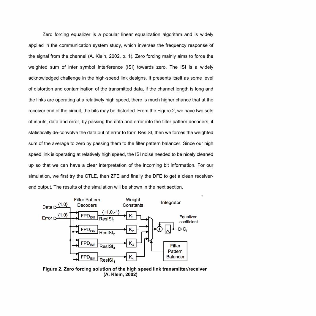
Zero forcing equalizer is a popular linear equalization algorithm and is widely
applied in the communication system study, which inverses the frequency response of
the signal from the channel (A. Klein, 2002, p. 1). Zero forcing mainly aims to force the
weighted sum of inter symbol interference (ISI) towards zero. The ISI is a widely
acknowledged challenge in the high-speed link designs. It presents itself as some level
of distortion and contamination of the transmitted data, if the channel length is long and
the links are operating at a relatively high speed, there is much higher chance that at the
receiver end of the circuit, the bits may be distorted. From the Figure 2, we have two sets
of inputs, data and error, by passing the data and error into the filter pattern decoders, it
statistically de-convolve the data out of error to form ResISI, then we forces the weighted
sum of the average to zero by passing them to the filter pattern balancer. Since our high
speed link is operating at relatively high speed, the ISI noise needed to be nicely cleaned
up so that we can have a clear interpretation of the incoming bit information. For our
simulation, we first try the CTLE, then ZFE and finally the DFE to get a clean receiver-
end output. The results of the simulation will be shown in the next section.
Figure 2. Zero forcing solution of the high speed link transmitter/receiver
(A. Klein, 2002)

The main purpose of using the zero forcing equalizer is to remove the precursor
echo of the pulse response in Figure 2. The highest cursor in the plot represents the
transmitted pulse signal. Since ZFE successfully removes all of the pre-cursors of the
signal, we can always see a negative pulse from the ZFE output. Though zero forcing can
remove the pre-cursor, which can be a distracting pulse in recognizing the signal, it still
has a pretty high post-cursor pulse (around 100mV in this simulation). This problem can
be fixed in Matthew’s DFE implementation.
The final eye output diagram after ZFE is shown below, together with the eye
output diagram without any equalization. From figure 3, the output eye diagram is very
messy and the signal is hardly readable. However, after applying ZFE, the output is much
cleaner and the distortion from the ISI has been greatly reduced.
In conclusion, applying ZFE completely removed the pre-cursor pulse of the
incoming signal though it introduces trouble post-cursor issues that are going to be solved
in DFE. To sum up, in the order of CTLE, ZFE and DFE, we gradually clean up the
incoming signal that is greatly interfered by the channel noises, which is of great
importance since out project aims to provide a high speed link library that can not only
run at a relatively high speed, but it also should never lose any data during its transmission.

The Matlab simulation gives us a good intuition and picture of what our final output of the
project should be, which is going to help us better modeling the circuit into the real
hardware.
4 Clock Data Recovery
4.1.1 Background
For the second semester, I am personally responsible for implementing the clock
data recovery block (CDR) using XMODEL, which is a simulation software we used for
this project. Given the fact that transmitter and receiver side of our high speed link are
driven by different clock source, even though the clock are generated with the same
frequency, we can’t guarantee that all the data samples will be sampled correctly.
Moreover, since the receiver-end of our high speed link has a much noisier and unstable
clock frequency compared to the transmitter side and potential clock drifts from the
system can even result in wrong sampling of the clock. In our case, we need to construct
a testbench environment to fully verify and simulate this link channel and come up with a
solution to extract and adapt clock signal from a relatively noisy clock frequency.
For our project, we need to construct a dual-loop clock and data recovery structure.
But in order to first verify the functionality of the CDR before integrate this module with
the phase interpolator and the other blocks, we choose to test with the bang-bang clock
and data recovery (BB-CDR) architecture which employs a bang-bang phase detector
from XMODEL. For this approach, the clock signal is generated by a receiver-side phase-
locked loop (Rx PLL) and we use this clock signal to sample the incoming data
information, meanwhile trying to synchronizing the income data with our clock signal. The

approximate flow of our architecture is shown below. The architecture can be divided into
three different phases: phase detection, digital filter and clock signal adaption from dco.
Figure 4. Alexander bang-bang Clock data recovery architecture [2]
The phase detection part of CDR is an alexander-type bang bang phase detector,
which have two XOR comparators and two data samplers for odd/even number of
incoming data signal. We have an output data bit from the sampler which is sent to the
DFE module for further decision making, the most important part is to use our generated
up/down signal bit from our comparator to adjust our sampling clock signal in real time.
In our current phase-locked testbench, we use the positive-edge of receiver-side clock to
sample our data signal and the negative-edge of the clock to sample the edge signal bit.
Then according to the following truth table shown in Table 1, the early signal bit is
generated by connecting the one cycle delay of the current data signal and one cycle
delay of the edge signal. On the other hand, the late signal is generated by xoring the
current data signal bit and the one cycle delay of the edge signal bit. The logic can be
summarized with the following table.

Data Signal Edge Signal Early Late
Dn-1 Dn En-1 En Xor(Dn-1, En-1) Xor(Dn, En-1)
Table 1. Xor logic to generate early/late signal from the Alexander phase detector
The second part of the architecture is our digital loop filter. We choose to have an
optimized Kp (proportional gain), Ki (integral gain) factor so that we can apply our loop
filter as a low pass filter. The low pass filter takes the output from the alexander phase
detector and accumulate the early/late bit information to attenuate the high frequency
component of the output. In our case, we use the digital filter with the most optimized PID
factors.
The last part of the CDR in the diagram is simply a clock generator, dco in this
case. Digitally controlled oscillator can adjust itself based on the output from the loop filter
and generate a new clock signal which has a frequency proportional to what we see from
the input data sequence.
4.1.2 Vectorization model of clock data recovery
The previous chapter of the introduction describes the bit-level clock data recovery
operation. However, the input to our CDR module is a vector of input. If we have a vector
length of 8, we need to correctly decode the bit information for different channels from a
serialized bit sequence. In order to achieve that we need to modify our bit-level
architecture to accommodate this new functionality by instantiating our data serializer
module . From Figure 5, we can easily see that for an 8-channel receiver input, we need
to decode the bit sequence accordingly into 8 parallel inputs, whose values will be

updated every N clock cycles. Before we can execute our computation for just 1 bit, after
the modification our period time for each channel is increased by a factor of N (vector
length). The deserializer module should be programmed to adjust to different length of
the vector.
Figure 5. Deserialization of a vector of bit input [4]
Second modification we need to do for the CDR architecture is the accumulation
adder part of the loop filter. Since we have a vector of N early/late bit signals from the
alexander phase detector, we need to have a “majority vote” logic to adjust our dco with
the most common late/early information for every clock cycle. To implement this
functionally, we have N parallel early signal bits and N parallel late signal bits generated
from the XOR logic which has been discussed before. Then we pass all of these bits
information into our decision module which simply counts the number of early/late signals
at the current clock edge. In short, if the total count of early is greater than the total count
of late signal, we need to pass early to the digital loop filter and vice versa.
4.2.1 Experiment Setup and Testbench
For this part of the project, since we are mainly dealing with digitalized bit signal,
we chose to use a relatively new tool called XMODEL. Since we, as a team, are working
on different parts of the project individually, XMODEL provides us a great platform to

simulate the entire high speed link and it is very easy to make some architectural
modifications with this tool. To fully verify the functionality of our created module, we start
from creating a simple testbench for the deserializer block. Figure 6 shows the output
from our simulation. The first signal is our running clock frequency, which is operating at
50Mhz. The second signal is the incoming randomly generated vector data. As we can
see, our deserializer works well and it correctly decodes the vector to four different
channel output, which is represented by the last four rows of waveform. For our modified
CDR block, we need to apply the same deserializer block to both even and odd digital
sample output and the deserialized data then are input to the XOR gates for further edge
detection/ computation.
Figure 6. Deserialization output for a vector length of 4
The second testbench we created is called lock acquisition, where we need to hook
up our other high speed data link modules in the XMODEL (transmitter, channel, CTLE,
DFE, etc) with our CDR block and perform a comprehensive verification for our overall
architecture. We first generate a 2.04GHz clock from the transmitter side and apply a
random generator to send a bit sequence data. The digitized bit stream is then converted
to an analog waveform with rise/fall time to better simulate our realistic high speed link
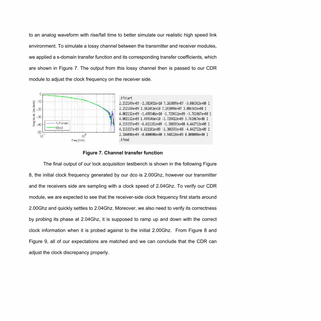
environment. To simulate a lossy channel between the transmitter and receiver modules,
we applied a s-domain transfer function and its corresponding transfer coefficients, which
are shown in Figure 7. The output from this lossy channel then is passed to our CDR
module to adjust the clock frequency on the receiver side.
Figure 7. Channel transfer function
The final output of our lock acquisition testbench is shown in the following Figure
8, the initial clock frequency generated by our dco is 2.00Ghz, however our transmitter
and the receivers side are sampling with a clock speed of 2.04Ghz. To verify our CDR
module, we are expected to see that the receiver-side clock frequency first starts around
2.00Ghz and quickly settles to 2.04Ghz. Moreover, we also need to verify its correctness
by probing its phase at 2.04Ghz, it is supposed to ramp up and down with the correct
clock information when it is probed against to the initial 2.00Ghz. From Figure 8 and
Figure 9, all of our expectations are matched and we can conclude that the CDR can
adjust the clock discrepancy properly.

Figure 8. Receiver-side clock frequency output
Figure 9. Receiver-side clock phase output (clock frequency=2.04Ghz)
5 Conclusion and Future Work
For the CDR module, we successfully develop and adapt our current CDR phase-
locking testbench to handle a vector of input streams, instead of a single bit. For the future
work, due to the time constraint and the fact that we need to find a way to convert the
current Systemverilog simulation environment into synthesizable Verilog codes, we can’t
finish the dual-phase CDR module and integrate it with the phase interpolator and the
other modules.

Chapter 2:
Project management
In this paper, we will discuss how we have structured the management roles of our
group as well as the division of labor for the technical hardware blocks in the link. Besides,
we will highlight the fact that when we build the link, we need to be aware of the IP
surrounding the technologies we are building with and the legal contracts we are bound
to. Finally, we will discuss the applications of our work within the University and future
projects this one makes possible.
The different blocks that we are building cover in different fields. Indeed, the signal
received is analog. It will then be processed and converted into a digital one. Then other
processing techniques will be applied on this signal. Thus, this kind of project requires a
broad knowledge and skills in the signal-processing field. Three main areas stand out:
analog design, mixed signal design and digital design. This kind of project perfectly fitted
our complementary knowledge as each one of us is specialized in one of this field. After
a general overview and design of the global infrastructure, our team split to dive into each
one of those parts.
IP issues
Unlike small social media startups, the way we try to commercialize our products
is very different and finally the buyers we target may not to be the entire public. Since we
are not building the real “hardware” infrastructure, which both needs a lot of infrastructure
and is relatively impossible for a small entry startup. We decide to take a similar approach
as ARM.inc does in the semiconductor industry. As we all know, ARM is one of the few
chip companies that actually never manufacture chips, instead they just design the
architecture IP and sell the IP to other semiconductors giants such as Intel and Apple.
Similarly, we try to generate our own high-speed link IP and sell it to our target tech
companies who need to research on their own data-center/chip infrastructures. In this
way, we don’t have to confront with the huge cost comes with manufacturing our new
high-speed design, which is both impossible for a startup and easily retaliated by the
industry leaders like Intel as soon as our product is released since it simply has more
resources. Moreover, our design mainly stems from Berkeley research groups and the
group of people who know and have experience in our cutting-edge technology is
relatively small, the chance of being substituted is relatively small given the unique nature
of our product.
Industry Analysis
We are not going to launch our product on the market. Indeed, our project is more
focused toward the academic field. However, if we want to understand what drives it, we
need to take a look at the current market.
As we stated before, there is a growing need of high-speed data links. Currently, this
project can subsist the needs of two main field of interest. The first one is the classic
modern chip design. As we increase the rates at which data transit inside a chip, we need
to provide links that can send data from one chip to another. This link has to endure those
speeds without deteriorating the quality of the initial signal. The main competitors on this
branch are the big tech companies like Intel, Broadcom, Nvidia, AMD.
The second field of application are the data centers. During the last decade, we have
seen the expansion of the flourishing industry of cloud computing. Indeed, we can see
that TE Connectivity, one of the biggest provider for backplanes, which are the channel

between the linecards inside a server, has an healthy situation, generation revenues of
$2.4 billion in 2016 (Darryle Ulama, 2016, p26). Those data centers are composed of
racks on which chips are linked through backplanes. In the wake of the general trend
described above, backplane links has to face an increasing demand of data speed. The
IBIS report on search engines in the US specifically highlights this point (Taylor Palmer,
2016, p34). In order to remains efficient and up to date, search engines has to constantly
index every web pages. Due to the huge amount of data, a large bandwidth is require in
order to offer instant search to everyone. The equipment deployed to cope with this are
more and more complex and the current capacity of Google’s data centers is assessed
at 1.13 petabits/s, which is 100 times more than ten years ago. Besides, during the last 6
years, the bandwidth has been multiply by a factor 50. This increasing bandwidth demand
leads us to develop links that are able to fill this demand so that the industry can keep
growing in the following years.
For our project, once we have a full and verified high speed link physical design,
we can run and verify it on relatively cheap multi-project wafer run and once qualified, we
can have it listed as an IP block with the foundry, so other customers like ASIC companies
can use it and pay the royalty for it.
Academic
Nevertheless, the initial purpose of our project is not to launch a product on the
market and compete with the other stakeholders. Indeed, due to the high constrains, it
takes a long time to design a link that can operates at those speed. Big companies are
already working on it and the price of their product can reach several tens of thousands
of dollars. However, some engineer need those links to develop their product. Thus, our

main goal is to provide an accessible technology to them so that they can work with it
without spending time on developing their own link. In that way, the library we will deliver
at the end of our project more echoes the needs of the academic field than the one of the
industry. The main advantage of this strategy is to provide at cheap library of high speed
links.
In that way, other researches will be able to rely on this infrastructure. For instance,
if they want to assess the quality of the signal they would have to cope with after receiving
the signal, they can use our library to do so.
6 Reference
1.Klein, G.K. Kaleh, P.W.Baier. “Zero forcing and minimum mean-square-error equalization for multiuser detection in code-division multiple-access channels”. IEEE Vehicular Technology Society, 06 Auguest 2002, 10.1109/25.492851 2.Scientific Analog, “XMODLE Simulating Bang-Bang CDR in XMODEL”, Jan 2017. 3. Takayuki Shibasaki, Win Chaivipas, Yanfei Chen, Yoshiyasu Doi, Takayuki Hamada, Hideki Takauchi, Toshihiko Mori, Yoichi Koyanagi, and Hirotaka Tamura, “A 56-Gb/s Receiver Front-End with a CTLE and 1-Tap DFE in 20-nm CMOS”, 2014 Symposium on VLSI Circuits Digest of Technical Papers 4. https://en.wikipedia.org/wiki/SerDes