high-speed and energy-efficient carry skip adder operating ... · in vlsi systems the area ......
TRANSCRIPT
International Journal of Emerging Technology in Computer Science & Electronics (IJETCSE) ISSN: 0976-1353 Volume 23 Issue 8 –NOVEMBER 2016.
13
Abstract— In this paper discussed about a carry skip adder (CSKA) structure with higher speed yet lower energy consumption compared with the conventional adder. In moreover, utilize multiplexer logic, the proposed structure make using NAND-NOR-Invert (NNI) and NOR-NAND-Invert (NNI) compound gates for the skip logic. The structure may be realized with both fixed and variable stage size styles, further improves the energy and speed parameters of the adder. Finally, a hybrid variable proposed adder structure, which lowers the power consumption affect the speed, is presented. The proposed architecture of this paper analysis the logic size, area and power consumption using Xilinx 14.2.
Index Terms— low power, high speed, CSKA, NNI.
I. INTRODUCTION
In VLSI systems the area efficient, low power and high performance are very important one in portable and mobile devices and biomedical instrument. The adder is the main component of the arithmetic operation of these devices. And also the several adders are used in complex digital processing. So the efficient adder is improving the performance of the DSP. Many numbers of adders are used for the arithmetic functions. The ripple carry adder is very simple adder. But the speed is less. Where as to use the carry look ahead adder is fastest one but the area consumption is high [1]. In [2], provide the performance of the 32 bit multiplier with carry look ahead adder and a 32 bit multiplier with ripple carry adder and showed that CLA multiplier is almost twice speed of the RCA multiplier.
We are proposed in this paper is carry skip adder; it is overcome the disadvantages of the Ripple carry adder and carry look ahead adder. So reduce the delay of the adder and reduce the area of the adder.
The rest of this paper to introduce the previous work for the paper is discussed in section II. Then, in section III, the adder of CSKA and hybrid CSKA are discussed. Section IV presents the simulation result of the paper. Finally Section V presents the conclusion of the paper.
II. PREVIOUS WORK
Adders are a key building block in arithmetic and logic units (ALUs) and hence increasing their speed and reducing their power/energy consumption strongly affect the speed and power consumption of processors. There are many works on the subject of optimizing the speed and power of these units, which have been reported. Obviously, it is highly desirable to achieve higher speeds at low-power/energy consumptions, which is a challenge for the designers of general purpose processors. One of the effective techniques to lower the power consumption of digital circuits is to reduce the supply voltage due to quadratic dependence of the switching energy on the voltage.
Moreover, the subthreshold current, which is the main leakage component in OFF devices, has an exponential dependence on the supply voltage level through the drain-induced barrier lowering effect. Depending on the amount of the supply voltage reduction, the operation of ON devices may reside in the super threshold, near-threshold, or subthreshold regions. Working in the super threshold region provides us with lower delay and higher switching and leakage powers compared with the near/subthreshold regions. In the subthreshold region, the logic gate delay and leakage power exhibit exponential dependences on the supply and threshold voltages. Moreover, these voltages are (potentially) subject to process and environmental variations in the nano-scale technologies. The variations increase uncertainties in the aforesaid performance parameters. In addition, the small subthreshold current causes a large delay for the circuits operating in the subthreshold region.
A. Conventional carry skip adder:
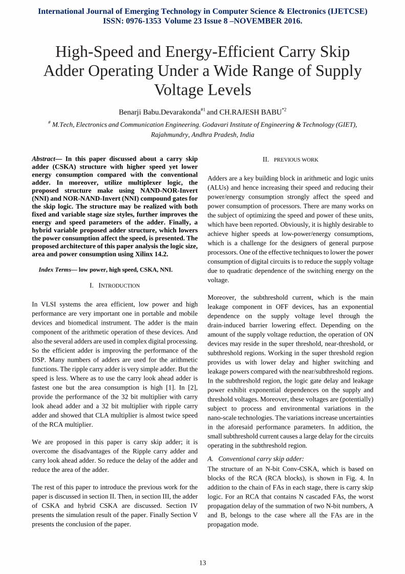
The structure of an N-bit Conv-CSKA, which is based on blocks of the RCA (RCA blocks), is shown in Fig. 4. In addition to the chain of FAs in each stage, there is carry skip logic. For an RCA that contains N cascaded FAs, the worst propagation delay of the summation of two N-bit numbers, A and B, belongs to the case where all the FAs are in the propagation mode.
High-Speed and Energy-Efficient Carry Skip Adder Operating Under a Wide Range of Supply
Voltage Levels Benarji Babu.Devarakonda#1 and CH.RAJESH BABU*2
# M.Tech, Electronics and Communication Engineering. Godavari Institute of Engineering & Technology (GIET),
Rajahmundry, Andhra Pradesh, India
International Journal of Emerging Technology in Computer Science & Electronics (IJETCSE)
ISSN: 0976-1353 Volume 23 Issue 8 –NOVEMBER 2016.
14
Figure 1: Conventional structure of the CSKA
It means that the worst case delay belongs to the case where Pi =Ai ⊕Bi =1fori =1... N
Where Pi is the propagation signal related to Ai and Bi. This shows that the delay of the RCA is linearly related to N. In the case, where a group of cascaded FAs are in the propagate mode, the carry output of the chain is equal to the carry input. In the CSKA, the carry skip logic detects this situation, and makes the carry ready for the next stage without waiting for the operation of the FA chain to be completed. The skip operation is performed using the gates and the multiplexer shown in the figure. Based on this explanation, the NFAs of the CSKA are grouped in Q stages. Each stage contains an RCA block with Mj FAs (j =1... Q) And skip logic. In each stage, the inputs of the multiplexer (skip logic) are the carry input of the stage and the carry output of its RCA block (FA chain). In addition, the product of the propagation signals (P) of the stage is used as the selector signal of the multiplexer. Fixed Stage Size CSKA:
By assuming that each stage of the CSKA contains MFAs, there are Q=N/M stages where for the sake of simplicity, we assume Q is an integer. The input signals of the jth multiplexer are the carry output of the FAs chain in the jth stage denoted byC0
j , the carry output of the previous stage (carry input of the jth stage) denoted by C1
j(Fig. 1). The critical path of the CSKA contains three parts: 1) the path of the FA chain of the first stage whose delay is equal to M×TCARRY; 2) the path of the intermediate carry skip multiplexer whose delay is equal to the (Q–1) ×TMUX; and 3) the path of the FA chain in the last stage whose its delay is equal to the (M−1) ×TCARRY+TSUM.
III. PROPOSED SYSTEM
A. Proposed hybrid variable latency CSKA:
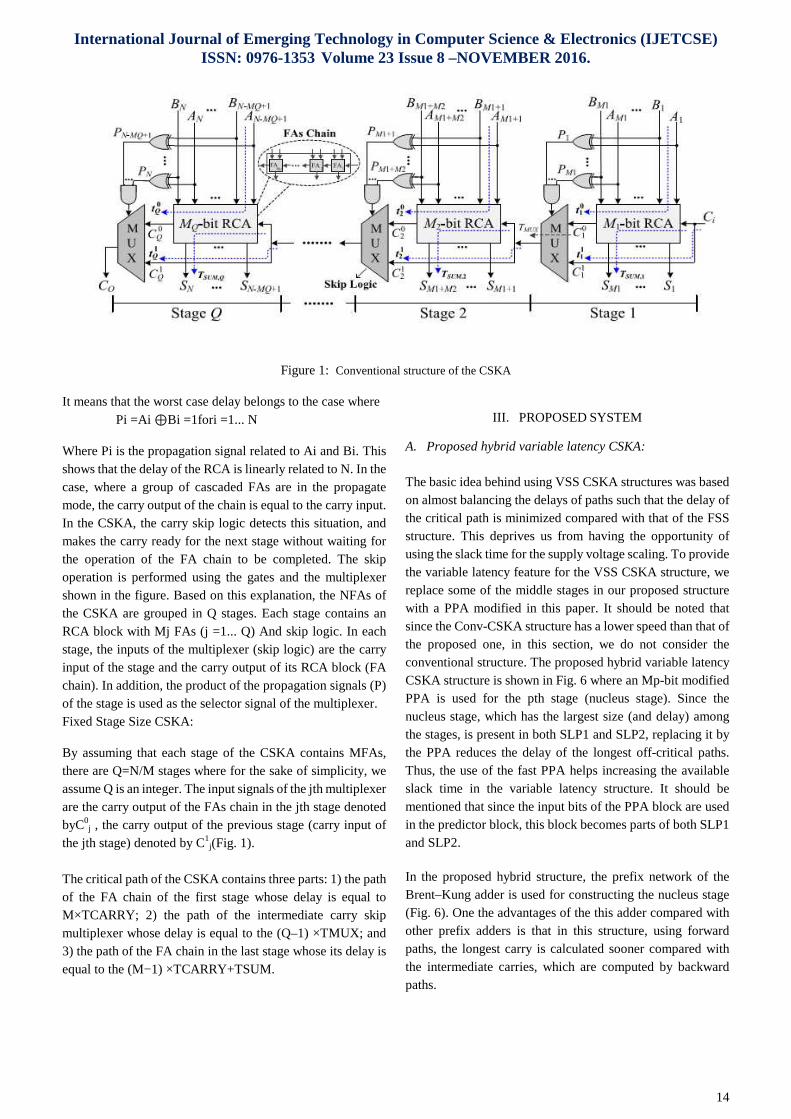
The basic idea behind using VSS CSKA structures was based on almost balancing the delays of paths such that the delay of the critical path is minimized compared with that of the FSS structure. This deprives us from having the opportunity of using the slack time for the supply voltage scaling. To provide the variable latency feature for the VSS CSKA structure, we replace some of the middle stages in our proposed structure with a PPA modified in this paper. It should be noted that since the Conv-CSKA structure has a lower speed than that of the proposed one, in this section, we do not consider the conventional structure. The proposed hybrid variable latency CSKA structure is shown in Fig. 6 where an Mp-bit modified PPA is used for the pth stage (nucleus stage). Since the nucleus stage, which has the largest size (and delay) among the stages, is present in both SLP1 and SLP2, replacing it by the PPA reduces the delay of the longest off-critical paths. Thus, the use of the fast PPA helps increasing the available slack time in the variable latency structure. It should be mentioned that since the input bits of the PPA block are used in the predictor block, this block becomes parts of both SLP1 and SLP2.
In the proposed hybrid structure, the prefix network of the Brent–Kung adder is used for constructing the nucleus stage (Fig. 6). One the advantages of the this adder compared with other prefix adders is that in this structure, using forward paths, the longest carry is calculated sooner compared with the intermediate carries, which are computed by backward paths.
International Journal of Emerging Technology in Computer Science & Electronics (IJETCSE) ISSN: 0976-1353 Volume 23 Issue 8 –NOVEMBER 2016.
15
Figure 2: Structure of the proposed hybrid variable latency CSKA.
In addition, the fan-out of adder is less than other parallel adders, while the length of its wiring is smaller.
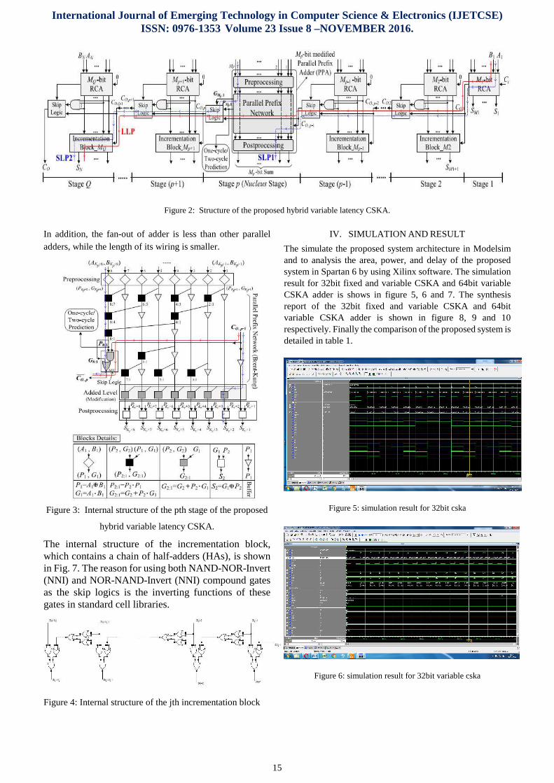
Figure 3: Internal structure of the pth stage of the proposed
hybrid variable latency CSKA.
The internal structure of the incrementation block, which contains a chain of half-adders (HAs), is shown in Fig. 7. The reason for using both NAND-NOR-Invert (NNI) and NOR-NAND-Invert (NNI) compound gates as the skip logics is the inverting functions of these gates in standard cell libraries.
Figure 4: Internal structure of the jth incrementation block
IV. SIMULATION AND RESULT
The simulate the proposed system architecture in Modelsim and to analysis the area, power, and delay of the proposed system in Spartan 6 by using Xilinx software. The simulation result for 32bit fixed and variable CSKA and 64bit variable CSKA adder is shows in figure 5, 6 and 7. The synthesis report of the 32bit fixed and variable CSKA and 64bit variable CSKA adder is shown in figure 8, 9 and 10 respectively. Finally the comparison of the proposed system is detailed in table 1.
Figure 5: simulation result for 32bit cska
Figure 6: simulation result for 32bit variable cska
International Journal of Emerging Technology in Computer Science & Electronics (IJETCSE)
ISSN: 0976-1353 Volume 23 Issue 8 –NOVEMBER 2016.
16
Figure 7: simulation result for 64bit variable cska
Figure 8: synthesis result for 32bit cska
Figure 9: synthesis result for 32bit variable cska
Figure 10: synthesis result for 64bit variable cska
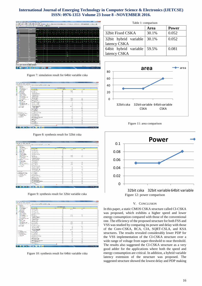
Table 1: comparison
Area Power 32bit Fixed CSKA 30.1% 0.052
32bit hybrid variable latency CSKA
30.1% 0.052
64bit hybrid variable latency CSKA
59.5% 0.081
0
20
40
60
80
32bit cska 32bit variable
CSKA
64bit variable
CSKA
area area
Figure 11: area comparison
0
0.02
0.04
0.06
0.08
0.1
32bit cska 32bit variable
CSKA
64bit variable
CSKA
Power
Figure 12: power comparison
V. CONCLUSION
In this paper, a static CMOS CSKA structure called CI-CSKA was proposed, which exhibits a higher speed and lower energy consumption compared with those of the conventional one. The efficiency of the proposed structure for both FSS and VSS was studied by comparing its power and delay with those of the Conv-CSKA, RCA, CIA, SQRT-CSLA, and KSA structures. The results revealed considerably lower PDP for the VSS implementation of the CI-CSKA structure over a wide range of voltage from super-threshold to near threshold. The results also suggested the CI-CSKA structure as a very good adder for the applications where both the speed and energy consumption are critical. In addition, a hybrid variable latency extension of the structure was proposed. The suggested structure showed the lowest delay and PDP making

International Journal of Emerging Technology in Computer Science & Electronics (IJETCSE) ISSN: 0976-1353 Volume 23 Issue 8 –NOVEMBER 2016.
17
itself as a better candidate for high-speed low-energy applications.
REFERENCES [1]. A. Tyagi, “A reduced area scheme for carry-select
adders”, IEEE Trans. on Computer, vol. 42, pp. 1163- 1170, 1993
[2]. Hasan Krad and Aws Yousif Al-Taie, “Performance Analysis of a 32-Bit Multiplier with a Carry-Look-Ahead Adder and a 32-bit Multiplier with a Ripple Adder using VHDL”, Journal of Computer Science 4 (4): 305-308, 2008.
[3]. Sauvagya Ranjan Sahoo, Kamala Kanta Mahapatra, "Design of Low Power and High Speed Ripple Carry Adder Using Modified Feed through Logic" in 2012 International Conference on Communications, Devices and Intelligent Systems (CODlS) , 978-1-4673-4700.
[4]. R.W.Doran, "Variants of an improved carry-Iook ahead adder," IEEE Trans. Computers, vol. 37, Sep.1988.
[5]. A Koren, Computer Arithmetic Algorithms, 2nd ed. Natick, MA, USA: A K Peters, Ltd., 2002.
[6]. R. Zlatanovici, S. Kao, and B. Nikolic, “Energy–delay optimization of 64-bit carry-look ahead adders with a 240 ps 90 nm CMOS design example,” IEEE J. Solid-State Circuits, vol. 44, no. 2, pp. 569–583, Feb. 2009.
[7]. S. K. Mathew, M. A. Anders, B. Bloechel, T. Nguyen, R. K. Krishnamurthy, and S. Borkar, “A 4-GHz 300-mW 64-bit integer execution ALU with dual supply voltages in 90-nm CMOS,” IEEE J. Solid-State Circuits, vol. 40, no. 1, pp. 44–51, Jan. 2005.
[8]. C. Nagendra, M. J. Irwin, and R. M. Owens, “Area-time-power tradeoffs in parallel adders,” IEEE Trans. Circuits Syst. II, Analog Digit. Signal Process., vol. 43, no. 10, pp. 689–702, Oct. 1996.
[9]. Y. He and C.-H. Chang, “A power-delay efficient hybrid carrylookahead/carry-select based redundant binary to two’s complement converter,” IEEE Trans. Circuits Syst. I, Reg. Papers, vol. 55, no. 1, pp. 336–346, Feb. 2008.
[10]. C.-H. Chang, J. Gu, and M. Zhang, “A review of 0.18 µm full adder performances for tree structured arithmetic circuits,” IEEE Trans. Very Large Scale Integr. (VLSI) Syst., vol. 13, no. 6, pp. 686–695, Jun. 2005.
[11]. D. Markovic, C. C. Wang, L. P. Alarcon, T.-T. Liu, and J. M. Rabaey, “Ultralow-power design in near-threshold region,” Proc. IEEE, vol. 98, no. 2, pp. 237–252, Feb. 2010.
[12]. R. G. Dreslinski, M. Wieckowski, D. Blaauw, D. Sylvester, and T. Mudge, “Near-threshold computing: Reclaiming Moore’s law through energy efficient integrated circuits,” Proc. IEEE, vol. 98, no. 2, pp. 253–266, Feb. 2010.
[13]. B. Ramkumar and H. M. Kittur, “Low-power and area-efficient carry select adder,” IEEE Trans. Very
Large Scale Integr. (VLSI) Syst., vol. 20, no. 2, pp. 371–375, Feb. 2012.