high spatial resolution gan and optical photon counting ... · pdf filefor photon counting...
TRANSCRIPT

High Spatial resolution GaN and Optical Photon Counting Detectors with sub-nanosecond
timing for Astronomical and Space Sensing Applications
Oswald Siegmund, John Vallerga, Barry Welsh, Anton Tremsin, Jason McPhate
Space Sciences Laboratory, U.C. Berkeley
ABSTRACT
Recent advances in UV-Visible ground and space borne detectors with the unique ability to record photon X,Y,T high fidelity information include the development of GaN UV photocathodes and cross strip high resolution position encoding readouts. Such sensors have the distinct advantage of being able to record the accurate time of each detected photon event, which is important for time dependent applications in space astronomy, biology, and time of flight instruments. Newly developed GaN photocathodes have achieved up to 80% quantum efficiency at 120 nm and in the opaque mode they demonstrate high efficiency up to a cutoff wavelength of about 360 nm. Meanwhile semitransparent GaN cathodes have achieved ~20% quantum efficiency in the 240 nm to 360 nm regime. Imaging devices with these photocathodes have demonstrated good spatial resolution and uniformity, with relatively low background event rates. For photon counting imaging detectors we have developed cross strip anode readouts with large, high spatial resolution formats capable of high counting rates and extended lifetimes. We have achieved resolutions of < 10 !m in tests over 32 mm x 32 mm anodes with excellent linearity. High-speed electronics for the cross strip readout are currently under development and should achieve > 1 MHz for random photon rates, and we have demonstrated time tagging of events to better than 1ns. A variety of sealed tube detectors are also in development with both GaN and GaAs photocathodes. Keywords: Microchannel plate, gallium nitride, photon counting, imaging, timing
1. INTRODUCTION
Microchannel plate (MCP) detectors can meet many of the challenging imaging and timing demands of various
applications, including astronomy of transient and time-variable sources, biological single-molecule fluorescence lifetime microscopy, LIDAR, airborne and space situational awareness, and optical night-time/reconnaissance (LANL-ASPIRE). Over the past decade we have implemented a variety of high-resolution, photon-counting MCP detectors in space instrumentation for satellite (FUSE [1], GALEX [2], IMAGE [3], SOHO [4], HST-COS [5]), rocket, and shuttle payloads as well as sensors for ground based astronomy, reconnaissance and biology. Sealed tubes with 25mm cross delay line anodes have been built for recording time resolved visible imaging of the Crab Nebula, for biological fluorescence lifetime imaging [6] and for the GALEX UV imaging satellite with 65mm active area. Open face detectors have also been used for photoelectron time resolved spectroscopy at the LBNL ALS synchrotron [7]. The 25mm aperture sealed tubes utilize S20 photocathodes deposited onto the input window, a stack of 3 MCPs to amplify the emitted photoelectrons, and cross delay line anodes to record the photon positions and times. The Crab pulsar was observed using the Lick observatory 1m telescope and the characteristic light curve shape [8] for the Crab was recorded with < 100 !s time resolution. The recorded data allows these to be optimally analyzed after the fact, without pre-knowledge of their position, seeing conditions, or pointing constraints. New sealed tubes with higher efficiency (Super GenII, GaAs) cathodes are in development, which in combination with larger telescope apertures (10m SALT telescope [8]) will provide enhanced sensitivity for future investigations.
There have been very few satellite instruments capable of high time resolution imaging in the UV. The Galactic Evolution Explorer (GALEX ) satellite [9], has accomplished unprecedented photometric imaging observations of astronomical sources in the near ultraviolet ([NUV] 1750 – 2750Å), and far ultraviolet ([FUV] 1350 – 1750Å). GALEX uses two sealed-tube photon counting detectors of 65mm active area [10, 11] with CsTe and CsI photocathodes, developed at University of California, Berkeley. During the course of sky-survey observations GALEX has serendipitously detected numerous variable and transient ultraviolet sources, including the passage of both asteroids and man-made satellites across the 1.2° field-of-view. Such objects are detectable in the UV due to reflection of the incident solar UV flux. GALEX records high time resolution photon event position information, so it is possible to reconstruct images as a function of time, and to determine the orbital path of the observed satellite, or asteroid.
Our recent work on efficient UV/optical photocathodes, ceramic MCPs and high performance photon counting imaging readouts enables significant advancements over the detector systems discussed above. Gallium Nitride (GaN, AlGaN, InGaN) photocathodes, cross strip image readouts, and ceramic MCPs show great promise for future detector applications. GaN in sealed tube detectors offers high QE across the UV (above 110 nm), with tailored cutoffs around 400 nm. Development efforts have yielded considerable advancement, with opaque GaN photocathode efficiencies up

to 80% at 120 nm and cutoffs at ~360 nm, with low out of band response, and high stability. Previous work with semitransparent GaN photocathodes produced relatively low QE (3%), however our recent data shows that QE of 15% to 25% can be achieved over a well defined band from 230nm to 360nm. We have also used 25mm active area semitransparent GaN photocathodes in an MCP two dimensional photon counting detector. The performance is quite good with reasonable image uniformity and high spatial resolution as well as fairly low intrinsic background (between 0.01 and 10 event sec-1 cm-2). GaN has also been deposited successfully on glass MCPs.
As the multiplication stage of the detector, ceramic MCPs offer the possibility to produce devices with small pores, excellent uniformity, high temperature capability, long lifetimes and low background compared with conventional glass MCPs. We have tested a number of alumina ceramic MCPs with sizes of 8 mm, 18 mm, 25 mm and pore sizes from 5 !m to 35 !m. We have also deposited GaN onto the alumina ceramic MCP substrates with promising results.
To obtain the highest event rates and spatial resolution at low MCP gain we have developed the Cross Strip (XS) anode. This anode uses charge division, and centroiding, of microchannel plate charge signals detected on two orthogonal layers of sense strips to encode event X-Y position, event time and signal amplitude. We have developed novel XS anode structures that can, in combination with small pore MCPs, perform at the highest spatial resolution levels with self triggered ~1 ns timing accuracy and encode photons and particles at greater than 1 MHz rates. For time of flight applications the individual events can also be time tagged to 100ps accuracy. Our development the XS charge division scheme has been demonstrated with circular, square, and rectangular formats, with sizes of 22mm, 32mm, and 45mm. Using custom parallel channel encoding electronics with FIR centroiding algorithms excellent resolution (better than 10 !m FWHM) has been achieved using low MCP gain (~ 106).
Various aspects of these developments are being used to produce open face and sealed tube imaging detectors for a wide range of photon and particle sensing tasks. Applications include the next generation of space astronomy imaging and spectroscopy missions (NASA SFO & USO missions), biological fluorescence lifetime imaging [12], ground based astronomical transient detection and variable source observations [8], optical night-time/reconnaissance [13] and time resolved X-ray fluorescence spectroscopy [7].
2. UV (GAN) AND VISIBLE PHOTOCATHODE DEVELOPMENT
The nitride-III semiconductors, and specifically GaN (band gap energy 3.5 eV), and related alloys AlxGa1-xN, are
potentially attractive as UV photocathodes for position sensitive detector systems. These can provide a broad coverage in the 150-400 nm wavelength regime below the various optical photocathodes (>400 nm, multi-alkali and GaAs). Currently CsTe (Fig. 1) is often used as a far ultraviolet semitransparent cathode, but has a fairly low efficiency (<20%), and cuts off at <300 nm. SupergenII alkali metal photocathodes (Fig. 1) provide better performance than
Fig. 1. Comparison of photocathodes for UV and visible Fig. 2. GaN cathode mounted (0.5 mm gap) into a MCP regimes including our recent GaN cathode (diamonds) data. detector with a 25mm cross delay line readout anode.

conventional S20 photocathodes, particularly in the red. Even better efficiency may be obtained in the visible with GaAs photocathodes, although it is necessary to employ modest cooling (0 °C) to reduce the background noise. We have made significant progress in the development of both opaque and semitransparent GaN photocathodes, are in the process of making sealed tube detectors with SupergenII cathodes, and have immediate prospects to make detectors with GaAs photocathodes. 2.1 GaN photocathode quantum efficiency measurements.
The attenuation characteristics of crystalline GaN indicate that the optimal thickness of a photocathode film should be between 100 and 200 nm, and ~20% of incident radiation is reflected, independent of wavelength and incident angle. Ideally, all photons would interact in the GaN layer as close to the emission surface as possible however this is not the case. Therefore, to promote electron drift to the surface, the GaN is Mg (p) doped (the minority carrier diffusion length in this material is ~200nm [14]), To further increase the probability of electrons reaching the emitting surface a thin barrier layer of AlN is deposited directly on the cathode substrate to create a potential barrier at the GaN/substrate boundary. Surface treatment of GaN with Cs is done as a last processing step to induce negative electron affinity. The relative merits of using opaque (front surface illumination and emission) and semitransparent (substrate side illumination and GaN front surface emission) depend largely on the achievable QE and the logical constraints of the device geometry. Both scenarios are being evaluated in our investigations.
Fig. 3. GaN QE measurements for opaque GaN samples Fig. 4. GaN cathode deposited onto an Alumina MCP On sapphire (107062001b11/b12), opaque GaN on an substrate with ~25 !m holes (107062601b11). alumina MCP substrate (107062601) and GaN deposited at low temperature onto fused silica (108031303).
We have made substantial progress in the fabrication of doped GaN layers and in cleaning and surface activation techniques, resulting in good photocathode performance repeatability. Based on the crystalline structure of GaN, we have normally used C-plane sapphire for the substrate material as it is a good match for CVD (chemical vapor deposition) or MBE (molecular beam epitaxy) deposition of GaN films. We have obtained MBE GaN samples (1” and 2” diameter) on sapphire from SVT associates. The SVT samples have a thin “reflective” layer of AlN (~10 nm) and a 100 nm to 250 nm GaN top layer Mg (p) doped. The most recent samples all include higher (1019 /cm3) P dopant (Mg) concentrations than those we have tried before, as well as depth graded doping profile to enhance the escape probability of the photoelectron from the photocathode surface into vacuum.
Key factors in cathode activation include cleaning techniques, degassing, vacuum scrubbing and surface activation with alkali metal (Cs). Many of these issues have been investigated, resulting in a basic process that has repeatedly achieved good photocathode performance. We measured (Fig. 3) sets of samples of crystalline and polycrystalline AlN/GaN coatings grown by MBE on sapphire substrates. Samples (150nm GaN, 107062001)(B11 and B12 are two different thermal processes) with high P dopant at the substrate are better (80% QE at 120nm) than higher surface P doped samples that have given the best results previously. We have also found that polycrystalline GaN performs as

well as crystalline GaN, thus allowing GaN to be grown on ceramic MCP substrates and tested (Fig. 3, Fig. 4). Alumina ceramic MCP substrates (Fig. 4) have been coated with GaN at high temperature without damage to the surfaces. The QE is not as good as the planar sapphire substrates, however we find that the bulk of the photoemission derives from the MCP pore area. In this case the pore area is only 25%, so substantial QE increases can be expected for more normal pore area fractions of ~65%. SVT associates have also developed a low temperature process that has allowed GaN cathodes to be coated onto fused silica and normal glass MCPs (Fig. 5). The initial QE results for GaN on fused silica are encouraging (Fig. 3) and GaN on a normal glass MCP will be tested shortly. The long wavelength response of the GaN photocathodes shows a significant drop between 360nm and 420nm (Fig. 6). Thereafter the drop off is somewhat slower, reaching a QE of ~10-6 at 600nm wavelength, which is much the same as seen by Mizuno et al [15].
Fig 5: GaN low temperature coating on a normal glass Fig. 6: GaN opaque QE measurements for several MBE MCP. The four quadrants have different GaN thicknesses. and CVD (NW-BH183-B04) grown samples showing the “out of band” response, and attenuation by 100 nm GaN.
Fig. 7. Schematic of a cross delay line readout MCP Fig. 8. GaN 0.15!m cathode on a sapphire substrate sealed tube detector with a GaN semitransparent cathode. mounted into a holder designed for the Fig. 2 detector.
2.2 GaN imaging detector tests
1” GaN/sapphire substrates were made for use in a 2D imaging tube detector demonstration device. The design (Fig. 7) uses a Sapphire/GaN semitransparent cathode in a holder. Due to the three wires used to hold down the substrate in the GaN deposition process, three “shadows” can be seen on the otherwise uniform green color of the

150nm GaN coating (Fig. 8). Fig. 7 shows the MgF2 entrance window with the GaN sample in its holder placing the GaN close (<0.5mm) to a MCP stack that is read out with a cross delay line anode. Our tests have enabled demonstration of the GaN cathode efficiency and spatial uniformity of response, verification of the background for GaN cathodes, and demonstration of 2D imaging properties. The gain and pulse height for single photon detection was very good (6 x 10⁶ gain, 50% FWHM). 254 nm illuminated images (Fig. 9) of a 1” GaN sample show the shadow of a tool wire (upper right), and the three GaN fabrication wire shadows. The general uniformity of the response is reasonable, but some GaN defects can be seen. These are directly related to damage in the cathode layer. The defect seen in the lower right of Fig. 8 is clearly imaged in Fig. 9, and Fig. 10, also showing the <50 !m spatial resolution of the detector. An obvious feature is the very high response (5x the general QE) in the thin layers where the mounting wires shadowed the GaN deposition. This is consistent for all of the samples and depth studies indicate that our optimization should be to consider layers slightly thinner than 100nm. Thus, we trade off the attenuation of light in the GaN, but allow higher escape probability for photoelectrons.
Fig 9. Image of a 0.15!m thick GaN cathode taken with . Fig. 10. Expanded view of the far right side of Fig.9. 254 nm light in semitransparent mode using 60v bias in Shows a GaN layer defect at high spatial resolution. the cross delay line detector shown in Fig. 2.
Fig 11. Background event image for a 0.15!m thick GaN. Fig. 12. GaN QE for semitransparent GaN. 0.15!m thick The rate is ~8 events sec-1 mm-2 for this sample. (107062001), 0.1!m thick (107062001), Mg ~2 x 1019 cm-3.

Another important parameter of photocathode operation is thermionic electron emission. The background images
(Fig. 11) of the 25mm sample(s) show a uniform distribution of events with rates of between <0.01 and 8 events mm-2 sec-1 which is commensurate with results of Mizuno et al [15], and varies significantly dependent on the Cs activation.
In semitransparent mode (Fig. 12) the GaN flat top QE response from 200nm to 400nm is expected (short end cutoff due to sapphire and AlN), but is consistently only 3 to 4% QE, compared with >60% photon absorption in the GaN layer (Fig. 12), while Mizuno [15] reports that as high as 25% can be achieved. Short wavelengths (that produce higher photoelectron energies) are absorbed closer to the incident surface of the GaN requiring the electrons produced to travel further in the GaN before escaping. They are thus attenuated and have less energy to escape when they reach the GaN surface. Longer wavelengths penetrate further and produce electrons closer to the emitting surface. The discovery that the thinner GaN layers produce 5x better QE (Fig. 9) indicates that up to 20% QE can be achieved. The data from our measurements of the general GaN surface have been adjusted by this enhanced area factor to show the expected result. Measurements on new samples are underway to confirm this and establish an optimal cathode design.
Fig. 13. Schematic of the operation of a cross strip anode Fig. 14. 45 mm x 45mm cross strip anode, with 72 x sealed tube detector. Photoelectrons emitted by the 72 orthogonal strips, connected by vias to the anode photocathode are multiplied by an MCP pair and produce backside. a sampled charge distribution on the strips of the anode.
3. CROSS STRIP DETECTOR SYSTEMS
The cross delay line detectors described above have been used for a number of applications including biological
fluorescence lifetime imaging [12], synchrotron excited photoelectron emission spectroscopy [7], time resolved astronomical observations from ground [8], space based instruments [9], and neutron imaging [16]. These uses have varying needs for their time accuracy, from none, to < 100 ps. The improvements in spatial resolution, counting rate and lifetime are most important for many potential future applications. To achieve these enhancements we have been developing the cross strip anode (Fig. 13). The cross strip (XS) anode is a relatively coarse (~0.5 mm) multi-layer metal and ceramic cross strip pattern on an alumina substrate (Fig. 14). On one surface of the substrate conductors are fabricated as a set of fingers approximately 0.5 mm wide. Then sets of insulating and conducting fingers are applied in the orthogonal direction such that 50 % of the bottom layer is left exposed, while keeping the crosstalk between axes negligible. The top and bottom layers are used to collect the charge from the MCPs with equal charge sharing between the axes.

Fig. 15. 40mm cross strip MCP detector in vacuum housing Fig. 16. PXS position encoding electronics boards, with RD20 preamplifier boards connected the X and Y axes. comprising a 64 channel 60MHz ADC (right) and a Xilinx Virtex 5 FPGA board (left).
Fig. 17. Image of a pinhole mask with 1 mm spacing, Fig. 18. Full resolution image of a single 10 !m mask 10 !m diameter holes. 40mm XS detector, gain 106, hole. 32 mm XS anode, MCP gain 1.5 x 10⁶. 10 !m MCP pores 6 !m. MCP pores (12.5 !m spaces). Two pores are resolved.
The anodes are low outgassing and accommodate >900°C temperatures, and may be put into sealed tube high
vacuum devices. The charge cloud is matched to the anode period so that it is collected on several neighboring fingers to ensure an accurate event centroid can be determined (Fig. 13). XS anodes are mounted ~3 mm behind the MCPs and each strip is connected through a hermetically sealed hole to the backside of the anode, allowing mounting of all the detector electronics outside the vacuum. We have previously reported results with a 32 x 32 mm XS open face laboratory detector, demonstrating excellent resolution (<7 !m FWHM) using low MCP gain (~5 x 10⁵) [17]. We have now made anodes up to 45mm x 45mm format (Fig. 14), as well as other smaller formats (Fig. 23). These are being utilized in both open face and sealed tube MCP detectors, for UV, visible and neutron detection and imaging.
To derive event positions each finger of an XS anode is connected to a charge sensitive amplifier (Fig. 15) and followed by subsequent analog to digital conversion (Fig. 16) of individual strip charge values and then calculation of event centroids. The center peak strip of the charge cloud distribution determines the coarse position of the registered
photon, and the charge cloud centroid is then calculated with precision to a fraction of a strip width. This can be accomplished by a hardware/software algorithms, which also account for amplifier gain variations, linearity and offsets.
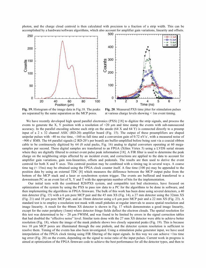
Fig. 19. Histogram of the image data in Fig.18. The peaks Fig. 20. Measured PXS time jitter for stimulation pulses are separated by the same separation as the MCP pores. at various charge levels showing < 1ns event timing.
We have recently developed high speed parallel electronics (PXS) [18] to digitize the strip signals, and process the events to generate the X, Y position with a resolution of <20 !m and time stamp the events with sub-nanosecond accuracy. In the parallel encoding scheme each strip on the anode (64 X and 64 Y) is connected directly to a preamp input of a 2 x 32 channel ASIC (RD-20) amplifier board (Fig. 15). The output of these preamplifiers are shaped unipolar pulses with ~40 ns rise time, ~160 ns fall time and a conversion gain of 0.72 nV/e-, with a measured noise of ~900 e- RMS. The 64 parallel signals (2 RD-20’s per board) are buffer-amplified before being sent via a coaxial ribbon cable to be continuously digitized by 64 (8 octal packs, Fig. 16) analog to digital converters operating at 60 mega-samples per second. These digital samples are transferred to an FPGA (Xilinx Virtex 5) using a LVDS serial stream where they are digitally filtered to extract event pulse peak information [18]. A FIR filter is used to determine the peak charge on the neighboring strips affected by an incident event, and corrections are applied to the data to account for amplifier gain variations, gain non-linearities, offsets and pedestals. The results are then used to derive the event centroid for both X and Y axes. This centroid position may be combined with a timing tag in several ways. A coarse time tag (< 15ns) may be obtained using the FPGA clock counter itself. A fine time (100 ps) may be appended to the position data by using an external TDC [8] which measures the difference between the MCP output pulse from the bottom of the MCP stack and a laser or synchrotron system trigger. The events are buffered and transferred to a downstream PC as an event list of X, Y and T with the appropriate number of bits for the implementation.
Our initial tests with the combined R20/PXS system, and compatible test bed electronics, have focused on optimization of the system by using the PXS to pass raw data to a PC for the algorithms to be done in software, and then implementing the algorithms in FPGA firmware. The bulk of this work has been done using several detectors, a 40 mm detector (Fig. 15) with a 6 !m pore MCP pair and the 45 mm XS (Fig. 14), a 27 mm detector using the 32mm XS (Fig. 21) and 10 !m pore MCP pair, and an 18mm detector using a 6 !m pore MCP pair and a 22 mm XS (Fig. 23). A standard test is to employ a resolution test mask with small pinholes at regular intervals to assess spatial resolution and image linearity. A result for the 40mm XS detector is shown in Fig. 17 which demonstrates a good image linearity, except for the outer periphery (1mm) where detector fringe fields deflect the electron clouds. The spatial resolution for this test was determined to be ~ 20 !m FWHM, and was found to be limited by errors in the signal correction tables that had doubled the “effective noise” level. Similar tests done with the 27 mm XS detector were able to achieve better resolution (Fig. 18), where the image of the mask pinhole shows two closely separated peaks (Fig. 19). This is because two 10 !m MCP pores are illuminated through the one pinhole, and the detector system resolution is sufficient to resolve them. Timing of the events has also been investigated. Using a stimulation pulse generator input, we have used interpolation of the FPGA clock timing using FIR filtering of the input signals. In this way we can achieve <1ns time tag error (Fig. 20) on the events, depending on the signal to noise ratio of the input pulses. Current work in progress is aimed at optimization of the FPGA firmware code to achieve the best performance for all the detector types, and then to
subsequently move from single event processing to multiple – closely spaced event handling to enhance the overall system counting rates.
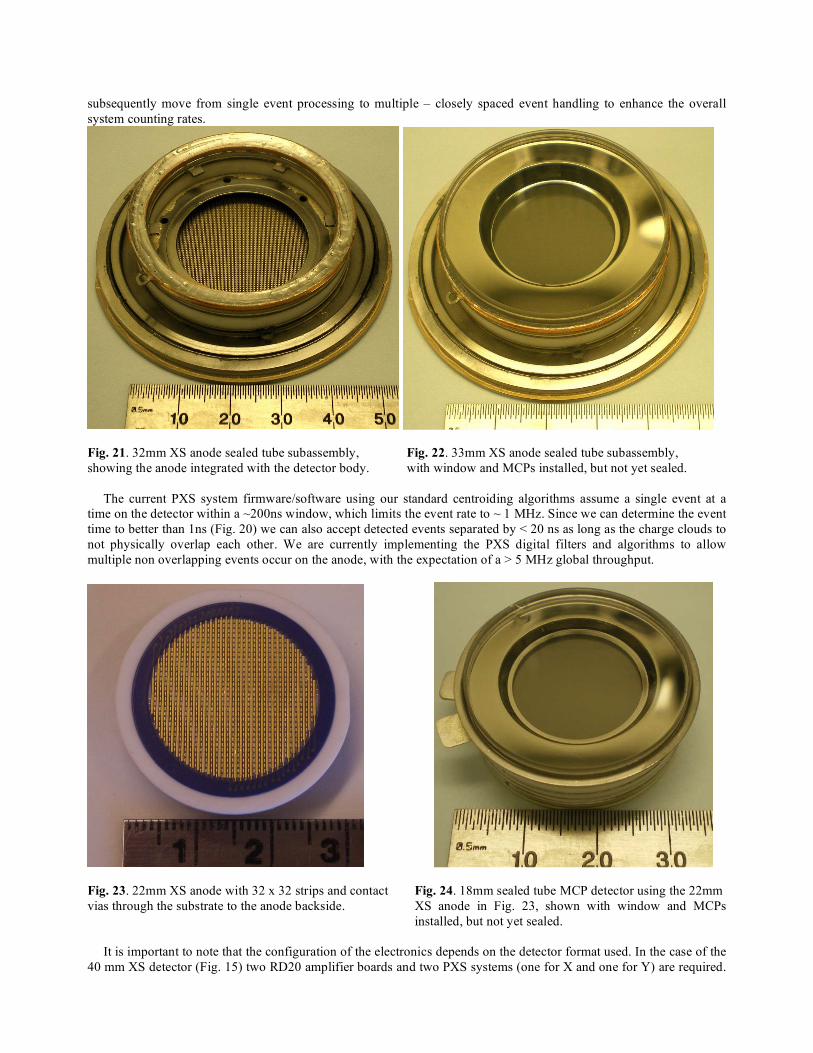
Fig. 21. 32mm XS anode sealed tube subassembly, Fig. 22. 33mm XS anode sealed tube subassembly, showing the anode integrated with the detector body. with window and MCPs installed, but not yet sealed.
The current PXS system firmware/software using our standard centroiding algorithms assume a single event at a time on the detector within a ~200ns window, which limits the event rate to ~ 1 MHz. Since we can determine the event time to better than 1ns (Fig. 20) we can also accept detected events separated by < 20 ns as long as the charge clouds to not physically overlap each other. We are currently implementing the PXS digital filters and algorithms to allow multiple non overlapping events occur on the anode, with the expectation of a > 5 MHz global throughput.
Fig. 23. 22mm XS anode with 32 x 32 strips and contact Fig. 24. 18mm sealed tube MCP detector using the 22mm vias through the substrate to the anode backside. XS anode in Fig. 23, shown with window and MCPs installed, but not yet sealed.
It is important to note that the configuration of the electronics depends on the detector format used. In the case of the 40 mm XS detector (Fig. 15) two RD20 amplifier boards and two PXS systems (one for X and one for Y) are required.

The same is true for the 32mm XS anode (27mm detector), which we are using as an open face detector but we are also building a sealed tube configuration (Fig. 21, Fig. 22) for use with visible (Supergen2) and UV photocathodes (GaN, in previous section). The 22mm XS anode (Fig. 23) requires only one RD20 board and one PXS system and is currently being tested as an open face device in our vacuum test facility. The 22mm XS is compatible with an 18mm format sealed tube detector (Fig. 24) and that will use a pair of 6!m pore MCPs. For the initial 18mm tubes we are currently building SuperGenII photocathodes (Photonis, Fig. 1) will be used for applications in biology [12], night-time remote sensing and ground based astronomy [8]. Ultimately GaAs photocathodes will replace the SuperGenII photocathodes increasing the efficiency with acceptable dark noise (< 100 events/sec) using cooling (-10°C).
6. ACKNOWLEDGEMENTS We acknowledge the efforts of R. Raffanti, Dr. X. Michalet, Dr. M. Ulmer, Synkera Technologies Inc., and SVT Associates Inc. for their assistance in accomplishing these studies. This work was supported in part by NSF grants AST0352980 and DBI-0552-096, NASA grants NAG5-12710 and NNG05GC79G, and NIH grant NIBIB R01 EB006353.
7. REFERENCES 1. O.H.W. Siegmund, M.A. Gummin, J.M. Stock, et. al, “Performance of the double delay line microchannel plate detect detectors
for the Far-Ultraviolet-Spectroscopic Explorer”, Proc SPIE 3114, pp.283-94, 1997. 2. O.H.W. Siegmund, P. Jelinsky, S. Jelinsky, et al., “High resolution cross delay line detectors for the GALEX mission”, Proc.
SPIE 3765, pp.429-40, 1999. 3. J.M. Stock, O.H.W. Siegmund, J.S. Hull, et al.,”Cross-delay-line microchannel plate detect detectors for the Spectrographic
Imager on the IMAGE satellite”, Proc SPIE 3445, pp.407-14, 1998. 4. O.H.W. Siegmund, M.A. Gummin, T. Sasseen, et al., “Microchannel plates for the UVCS and SUMER instruments on the
SOHO satellite”, Proc. SPIE 2518, pp.334-55, 1995. 5. Vallerga, J.; Zaninovich, J.; Welsh, B.; Siegmund, O.; McPhate, J.; Hull, J.; Gaines, G.; Buzasi, D. The FUV detector for the
cosmic origins spectrograph on the Hubble Space Telescope, Nuclear Instruments and Methods in Physics Research Section A, Volume 477, Issue 1-3, p. 551-555, 2002.
6. O. Siegmund, J. Vallerga, P. Jelinsky, M. Redfern, X. Michalet, S. Weiss, “Cross Delay Line Detectors for High Time Resolution Astronomical Polarimetry and Biological Fluorescence Imaging“, IEEE 2005 Nuclear Science Symposium and Medical Imaging Conference, Puerto Rico, October 2005.
7. A.S. Tremsin, G.V. Lebedev, O.H.W. Siegmund, et al, High spatial and temporal resolution photon/electron counting detector for synchrotron radiation research, Nucl. Instrum. and Meth. A, 580, 853-857, 2006.
8. O.H.W. Siegmund, J. McPhate, A. Tremsin, J.V. Vallerga, B.Y. Welsh and J.M. Wheatley, AIP Conference Proceedings, 984, 103, 2008.
9. D. C. Martin, J. Fanson, D. Schiminovich, et al., “The Galaxy Evolution Explorer: A space ultraviolet survey mission”, Astrophysical Journal 619, pp. L1-L6, 2005
10. P. Jelinsky, P. Morrissey, James Malloy, S. Jelinsky, and O. Siegmund, C. Martin, D. Schiminovich, K. Forster, T. Wyder & P. Friedman, “Performance Results of the GALEX XDL detectors”, Proc. SPIE, 4854, p.233-240, 2002.
11. O. Siegmund, P. Jelinsky, S. Jelinsky, J. Stock, J. Hull, D. Doliber, J. Zaninovich, A. Tremsin, K. Kromer, "High-resolution cross delay line detectors for the GALEX mission", Proc. SPIE, 3765, pp. 429-440, 1999.
12. Michalet, X.; Siegmund, O. H. W.; Vallerga, J. V.; Jelinsky, P.; Millaud, J. E.; Weiss, S., Photon-counting H33D detector for biological fluorescence imaging, Nuclear Instruments and Methods, Section A, Vol. 567, Issue 1, p. 133-136. 2006.
13. W. Priedhorsky and J. Bloch, Applied Optics, 44(3), 423-433, 2004. 14. Nemanich RJ, Baumann PK, Benjamin MC, Nam OH, Sowers AT, Ward BL, Ade H, Davis RF, Applied Surface Science, 132,
694-703, 1998. 15. Mizuno, I. T. Nihashi, T. Nagai, M. Niigaki, Y. Shimizu, K. Shimano, K. Kato, T. Ihara, K. Okano, M. Matsumoto, M.
Tachino, Proc. SPIE 6945-54, 2008. 16. O.H.W. Siegmund J.V. Vallerga, A. Martin, B. Feller, M. Arif. D. Hussey, and D. Jacobsen, A high spatial resolution event
counting neutron detector using microchannel plates and cross delay line readout, Nucl. Instrum. and Meth. A, 579, 188-191, 2006.
17. A. S. Tremsin, O. H. W. Siegmund, J. V. Vallerga, J. Hull, IEEE Trans. Nucl. Sci. 51, pp.1707-1711, 2004 18. O.H.W. Siegmund, A. Tremsin, J.V. Vallerga, J. McPhate, “microchannel plate cross strip detectors with high spatial and
temporal resolution”, submitted to Nuclear Instruments and Methods, 2008.