high q terahertz photonic crystal microcavities · high q terahertz photonic crystal microcavities...
TRANSCRIPT

UNIVERSITY OF CALIFORNIA
Santa Barbara
High Q Terahertz Photonic Crystal Microcavities
A Dissertation submitted in partial satisfaction of the
requirements for the degree Doctor of Philosophy
in Physics
by
Cristo Manuel Yee Réndon
Committee in charge:
Professor Mark S. Sherwin, Chair
Professor S. James Allen
Professor Leon Balents
December 2009

The dissertation of Cristo Manuel Yee Rendon is approved.
____________________________________________
Professor Leon Balents
____________________________________________
Professor S. James Allen
____________________________________________
Professor Mark S. Sherwin, Committee Chair
September 2009

iii
High Q Terahertz Photonic Crystal Microcavities
Copyright © 2009
by
Cristo Manuel Yee Rendon

iv
To my parents:
Manuel Yee Gonzales
and
Manuela Rendon Sanchez

v
ACKNOWLEDGEMENTS
I like to start thanking my advisor Professor Mark S. Sherwin for his patience,
support and resourceful guidance through all the five years that I worked under his
supervision, for all the personal meeting in which he always no only encourage me
but also point out the most efficient and elegant way to solve problems.
Then I would like to thanks the member of my committee, Dr. James Allen and
Dr. Leon Balents for helping to improve my thesis project.
I also want to thanks my colleagues Nathan Jukam who him I work during my
first year in the group and from whom I learned most of the fine details of clean
room processing. Susumu Takahashi who has a extraordinary ability to completely
construct an lab from the floor to the ceiling, and who makes a complicated subject
looks simple. To Dominik Sther from who I learn that loot can be done in single
afternoon if you know what you are doing. Also I would like to thank to Stephen
Parham who help in the lab in work in which I am not particular patient.
I would like to thanks to the present and former members of my research group
from who I spend quite nice lab time. Sangwoo Kim, Christopher Morris, Ben Zacks
and Dan Allen. Also a very special mention to Dr. Louis Claude Brunel from whom
I share my office but we also share a lot of good conversations from history to
family issues an extraordinary experience I always will remember he shown that
there is also a “Sueño Mexicano”. Special thanks to Michael Champion and George
Kontsevich for proofreading my thesis.

vi
Thanks to the undergrad students that worked with me during different research
projects, Stephen Parham, Kayla Nguyen and George Kontsevich.
I want to thanks to Clean room staff, Jack Whaley, Luiz Zunuaga, Brian
Thibeault and specially to Donald Freeborn for recovering my shatter samples from
inside the etching chambers. Thanks to Physics machine shop staff Mike Deal, Mike
Wrocklage and Jeff Dutter. Thanks to the FEL staff David Enhart and Gerry Ramian.
I would like to take a lot to the staff in the ITST, to chief Marlene Rifkin, to Kate
Ferrian for it sweets moments. To Rita Makogon, Elizabeth Strait, Jose and Rob
Marquez. To the staff member in the physics department, to Jennifer Farrar, Shilo
Tucker and Kerri O'Connor. To the people at UC-MEXUS program Dr. Wendy
DeBoer, Susana Hidalgo and Clara Quijano. And to the staff member at CONACYT
Veronica Barrientos and Samuel Manterola.
I also want to thanks to the Mexican National Council of Science and
Technology, to University of California Institute for Mexico and United States, to
the National Science foundation and to Keck foundation for their generous support.
Thanks to Dr. Maximo Lopez Lopez my former adviser in Mexico City, to Dr.
Juan Antonio Nieto Garcia my advisor as undergrad student. To Dr. Miguel Angel
Perez Angon. Thanks to Hector Uriarte, Dr. Servando Aguirre, Dr. Maribel Loaiza
and Carlos Valencia.
Finally but not least important I would like to thanks to persons to who I
dedicated not only work but my life as well, to my parents Manuel Yee Gonzalez
and Manuela Rendon Sanchez from wh always inspired me and push me forward, to

vii
my brothers and sisters Ana, Zumey, Bruce and Arturo Yee Rendon. To my
grandparents Manuel Yee Lam, Ruperta Gonzalez, Bernabe Rendon and Julia Lopez.
Thanks to my wife Lorena Ruiz de Yee who inspired me and help me to reach higher
altitudes that I will definitively never will have done alone, and thanks to my
beautiful daughter Sarah Sophia Yee Ruiz who changed my life completely and give
me a powerful reason to complete my goals.
Thanks you all for helping me to the complete my academic education.

viii
VITA OF CRISTO MANUEL YEE RENDON
September 2009
EDUCATION
September 1995 – August 2000
Bachelor of Sciences in Physics
School for Physics and Mathematics, Autonomus University of Sinaloa
Culiacan, Sinaloa, Mexico.
August 2000 – March 2003
Master of Sciences in Physics
Physics Department, Center for research and advanced studies, IPN.
Mexico City, Mexico.
March 2005 – September 2009
Doctor of Philosophy in Physics
Physics Department, University of California
Santa Barbara, California, USA.
PROFESSIONAL EMPLOYMENT
September 2003 – December 2004
Teaching Assistant
Department of Physics, University of California, Santa Barbara

ix
December 2004 – September 2009
Graduate Student Researcher
Terahertz Dynamics and Quantum Information in Semiconductors Lab.,
Department of Physics and Institute for Terahertz Science and Technology,
University of California, Santa Barbara
PUBLICATIONS
[1] Cristo M. Yee and Mark S. Sherwin, "High-Q terahertz microcavities in
silicon photonic crystal slabs.", Applied Physics Letters, vol. 94 , p. 154104 ,
(2009).
[2] Cristo Yee, Nathan Jukam, and Mark Sherwin, "Transmission of single mode
ultrathin terahertz photonic crystal slabs.", Applied Physics Letters, vol. 91 ,
no. 19, pp. 194104-3, nov (2007).
[3] Nathan Jukam, Cristo Yee, Mark S. Sherwin, Ilya Fushman, and Jelena
Vučković, "Patterned femtosecond laser excitation of terahertz leaky modes
in GaAs photonic crystals.", Applied Physics Letters, vol. 89 , no. 241112,
(2006).
[4] C. M. Yee-Rendón, A. Pérez-Centeno, M. Meléndez-Lira, G. González de la
Cruz, M. López-López, Kazuo Furuya, Pablo O. Vaccaro. “Interdiffusion of
Indium in piezoelectric InGaAs/GaAs quantum wells grown by molecular

x
beam epitaxy on (11n) substrates.”, Journal of Applied Physics 96, 3702
(2004).
[5] C.M. Yee-Rendón, M. López-López, and M. Meléndez-Lira, "Influence of
Indium segregation on the ligth emission of piezoelectric InGaAs/GaAs
quantum wells grown by molecular beam epitaxy.", Revista Mexicana de
Física vol. 50, 193 (2004).
[6] J.A. Nieto, M.P. Ryan, O. Velarde and C.M. Yee, “Duality symmetry in
Kaluza-Klein (n + D + d)-dimensional cosmological model.”, International
Journal of Modern Physics A, vol. 19, 2131 (2004).
[7] J.A. Nieto and C.M. Yee, “p-brane action from gravidilaton effective action”,
Modern Physics Letters A, vol. 15, 1611 (2000).
CONFERNCE PRESENTATIONS
[1] Materials Research Society (MRS) Spring meeting, San Francisco, CA (talk,
2009)
[2] International Workshop on Optical Terahertz Science and Technology
(OTST), Santa Barbara, CA (talk, 2009)
[3] American Physical Society (APS) March meeting, New Orleans, LA (talk,
2008)
[4] American Physical Society (APS) March meeting, Denver, CO (talk, 2007)

xi
HONORS
[1] Mexican National Council of Science and Technology – University of
California Institute for Mexico and United States Scholarship, September
2003 to August 2008.
[2] Mexican National Council of Science and Technology Scholarship, August
2000 to August 2002.
[3] Telmex Foundation Scholarship, September 1997 to August 2002.
[4] Autonomous University of Sinaloa Academic Scholarship, September 1998
to August 2000.

xii
ABSTRACT
High Q Terahertz Photonic Crystal Microcavities
by
Cristo Manuel Yee Rendon
We present a study of terahertz photonic crystal structures consisting of photonic
crystal slabs, photonic crystal waveguides and photonic crystal cavities. The
structures were fabricated from high resistivity silicon wafers using deep reactive ion
etching. The photonic crystals were based on a triangular array of hole for which for
hole size r=0.30a has a photonic gap for transversal electric polarization and for hole
size r=0.45a it has a optical gap for transversal magnetic polarization, where a is the
lattice constant.
We fabricated samples to operate at 1 THz for transversal electric and transversal
magnetic polarizations which were intended to be coupled to quantum transitions in
nanostructures or hydrogen like transitions of impurities in semiconductors which lie
near 1 THz. The optical gaps for the photonic structures were measured using far
infrared spectroscopy and time domain spectroscopy. Cavities were constructed and
inserted into a waveguide forming a narrow band Lorentzian filter. For transversal
electric (transversal magnetic) polarization we used an L3 (L2) which consist in

xiii
three (two) holes missing along the ΓJ orientation. The transmittance measurements
using a narrow band source present sharp resonances associated with the resonant
modes of the cavity. A quality factor as high a 1020 for transversal electric and 1560
for transversal magnetic were found.
We also studied the 240 GHz range. Here the cavity is intended to be
incorporated into a 240 GHz electron spin resonance setup. Here we used the L3
cavity for transversal electric polarization. The photonic crystal cavity was coupled
to a waveguide using the Lorentzian coupling and channel drop scheme.
Transmittance measurements and scattering into free space by the cavity employing
a narrow band source reveals a Q factor as high as 3800.
Frequency domain and finite time domain measurements using the experimental
parameter of the structures accurately predict the values found in the experiment.

xiv
TABLE OF CONTENTS
1 Motivation and overview ............................................................................ 1
A. Motivations ....................................................................................... 1
B. Objectives .......................................................................................... 4
C. Thesis structure ................................................................................. 5
2 Theoretical Foundations .............................................................................. 6
A. Photonic crystals ............................................................................... 6
B. Photonic crystal cavities .................................................................. 14
C. Photonic crystal waveguide ............................................................. 15
3 Photonic crystal Design and Fabrication ................................................... 17
4 Terahertz Photonic crystal slab ................................................................. 21
A. . Experimental setup ........................................................................ 22
B. Sample fabrication .......................................................................... 24
C. Experimental results and discussion ............................................... 26
D. Conclusion: optical gap for a THz TE photonic crystal slab .......... 29
5 Transversal Electric Photonic Crystal Cavity ........................................... 31
6 Transversal Magnetic Photonic crystal cavity .......................................... 45
A. Sample Fabrication .......................................................................... 46
B. Photonic crystal gap measurements ................................................ 48
C. Photonic crystal gap theoretical calculation .................................... 55
1. Two dimensional calculation ...................................................... 56
2. Three dimensional calculation .................................................... 58
xv
D. Cavity mode measurements ............................................................ 64
E. Cavity mode theoretical calculation ................................................ 73
1. Two dimensional cavity modes ................................................... 74
2. Three dimension cavity modes .................................................... 82
7 High-Q photonic crystal cavity for 0.24 THz electron spin resonance. .... 85
A. Photonic crystal resonance as a function of the length of the barrier
in a Lorentzian filter .................................................................................. 94
B. Photonic crystal resonance as a function of the hole displacement
in the barrier for a Lorentzian filter ........................................................... 97
C. Photonic crystal resonances in the channel drop configuration. ... 105
D. Summary for the 240 GHz cavities. .............................................. 115
8 Conclusions ............................................................................................. 116
Appendix A. Eigen Value problem Maxwell equations. .......................................... 118
Appendix B. Bloch Theorem. ................................................................................... 121
A. Reduced Zone scheme ................................................................... 124
Appendix C. Mode Couple Theory. ......................................................................... 128
A. Lorentzian Filter ............................................................................ 128
B. Lorentzian Filter with losses ......................................................... 137
C. Channel drop configuration ........................................................... 141
Appendix D. Fabrication recipes. .............................................................................. 149
A. Carrier wafer coating ..................................................................... 149
B. Handling wafer preparation ........................................................... 150
xvi
C. Lithography process ...................................................................... 150
1. TE photonic crystal samples 1 THz .......................................... 151
2. TM photonic crystals sample 1 THz ......................................... 151
3. TE photonic samples 240 GHz ................................................. 152
D. Etching process ............................................................................. 152
E. Unmount of the wafers .................................................................. 154
F. Edge removal ................................................................................ 155
Appendix E. Thin sample thickness measurement. .................................................. 156
A. Photonic crystal slab samples ........................................................ 157
B. High Q photonic crystal samples .................................................. 158
Appendix F. MPB and MEEP files. ......................................................................... 160
A. MPB : band diagram of a Photonic crystal ................................... 160
1. Specific parameters: .................................................................. 160
2. CTL file ..................................................................................... 161
3. Examples ................................................................................... 162
B. MEEP: Waveguide dispersion relation ......................................... 162
1. Specific parameter ..................................................................... 162
2. CTL file ..................................................................................... 163
3. Examples ................................................................................... 164
C. MEEP: Transmittance through the photonic crystal ..................... 164
1. Specific parameters ................................................................... 165
2. CTL files ................................................................................... 165

xvii
3. Examples ................................................................................... 166
D. MEEP: L3 Cavity resonance ......................................................... 167
1. Specific parameters ................................................................... 167
2. CTL file ..................................................................................... 167
3. Examples ................................................................................... 169
E. MEEP: L3 Lorentzian filter .......................................................... 169
1. Specific parameters ................................................................... 169
2. CTL file ..................................................................................... 170
3. Examples ................................................................................... 171
F. MEEP: L2 Lorentzian filter .......................................................... 171
1. Specific parameters ................................................................... 172
2. CTL file ..................................................................................... 172
3. Examples ................................................................................... 173
G. MEEP: L3 Channel drop ............................................................... 173
1. Specific parameters ................................................................... 173
2. CTL file ..................................................................................... 174
3. Examples ................................................................................... 175
Appendix G. Sample inventory. ................................................................................ 176
A. Photonic crystal gap 1.4 THz ........................................................ 176
B. TE Photonic crystal waveguide and cavities at 1 THz .................. 176
C. TM Photonic crystal waveguide and cavities at 1 THz ................. 176
D. TE 240 Waveguide and Photonic crystal cavity ........................... 177

xviii
1. Direct coupling scheme ............................................................. 177
2. Channel drop coupling .............................................................. 177
References ................................................................................................................. 178

1
1 Motivation and overview
The terahertz domain is located at the heart of the electromagnetic spectrum. It is
commonly accepted to cover the range from 0.3 to 30 THz. This region marks a
transition zone where electronic and photonic technologies converge, a place that up
to now has been considerably challenging due to the non trivial way to produce and
detect radiation but also a place where significant improvements could be made.
Science at terahertz frequencies is a very active region of research as many
physical phenomena are in its scope. The black body radiation of an object with
temperature above 10K emits in the terahertz region. Collective modes in polar
liquids, like water, absorb at terahertz frequencies. Biological systems are also in
this range as collective motions in proteins occur at terahertz frequencies Quantum
transitions in nanostructure like intersubband transitions in quantum wells and
quantum dots lie in the terahertz regime [1,2,3,4,5]
A. Motivations
Among the interesting research topics studied at terahertz frequencies is the
proposal for a quantum information scheme based in a terahertz quantum system. In
particular the proposal that motivated the present work is the one formed by the 1s-
2p transition of shallow donors in GaAs as a qubit and a terahertz photonic crystal
cavity as the resonator.
Photonic crystal cavities have the properties that they could reach extremely high
Q values and very small modal volume, properties required in order to reach the

2
strong coupling regime needed for the implementation of quantum information
schemes. A high Q cavity is also useful not only for quantum information but also
for applications where strong localized fields are needed, as in the case of compact
sensors and filters and low-threshold lasers [6,7].
The quantum transition 1s-2p for an ensemble of shallow donors in GaAs has a
typical energy of 4mev and a inhomogeneous line width of 𝛾𝑄 = 15 GHz and for a
moderate Q=1000 we have that the linewidth 𝛾𝐶 = 1 𝐺𝐻𝑧. The coupling strength of
an ensemble of donors to a cavity mode is given by Ω = 𝑁𝑔0, where N is the
number of donors coupled in the cavity and 𝑔0 is the coupling strength for a single
donor. For a moderated doping of 𝑛 = 4 × 10²⁰ 𝑚−3 the cavity strength coupling is
given by Ω = 175 𝜇𝑒𝑉 ≈ 42 𝐺𝐻𝑧 . With these values the condition for strong
coupling Ω ≥ 𝛾𝑄 − 𝛾𝐶 4 is satisfied.
High Q cavity could lead to produce extremely low threshold lasers by using the
intersub-level transition in quantum dots. Recently quantum posts [8], have been
proven to have intersub-level transitions at terahertz frequencies. Quantum posts
have the advantage their energy transitions could be tuned by changing the size of
the post. The integration of a quantum post into a terahertz photonic crystal opens
the opportunity to produce an extremely low threshold lasers. In particular we
explore the possibility of constructing a photonic crystal cavity that will couple to
quantum posts. A quantum post transition has a strong dipole along the growth axis
and therefore requires a cavity with electric field polarized in the same direction.
According to the conventions of photonic crystals, such a cavity has a transverse

3
magnetic (TM) polarization. Most of the work has been done for transverse electric
(TE) polarized cavities and therefore a high Q TM cavity is worth exploring.
A high Q cavity with small mode volume will be beneficial to a high frequency
electron spin resonance (ESR). High fields enhance the sensitivity of this technique,
and in particular we look to integrate a photonic crystal cavity to the UCSB 240 GHz
ESR spectrometer. Electron spins in Si are of particular interest. The lifetime of
donor electron spins in phosphorus-doped silicon is extremely large [9,10], and it’s
been proposed as a qubit.bFor this particular quantum system, the line width of the
transition is 𝛾𝐶 ≈ 7𝑀𝐻𝑧 and for a doping density 𝑛 = 1 × 10²¹𝑚−3 an ensemble of
spins has a coupling strength Ω ≈ 8.85 𝑀𝐻𝑧. For reaching the regime of strong
coupling it will be required to have a cavity with a line width of 25 MHz or less
which at 240 GHz correspond to a cavity with a quality factor Q=9600, a Q value
that is within the reach of a photonic crystal cavity.
The construction of photonic crystal cavities that couple to the three THz
schemes that we mentioned before, shallow impurities in GaAs, terahertz quantum
nanostructures, in particular quantum posts, and electron spin resonances are the
motivation behind our work.
Photonic crystals at terahertz frequencies has been constructed mainly intended
to be used for terahertz quantum cascade lasers; here the mode is lateral confined by
a two dimensional photonic crystal while the vertical confinement is produced by
double wall metal waveguide; using this simple structure very small threshold laser
have been constructed. However a real photonic cavity in which the modes are

4
strongly confined will push even further the laser threshold, this dielectric cavity has
not been constructed yet. The main obstacle is not the construction of the cavity
itself, as there a lot of examples of photonic crystal structures and applications based
on THz photonic crystals [11,12,13,14,15,16,17,18], but in its characterization. One
way to characterize a photonic crystal cavity is by having a source inside the cavity
[19], however there is not a THz emitter that could be used for this purpose. Another
way to measure a photonic crystal cavity is by coupling the cavity to a waveguide
[20], however at THz frequencies there a very few tunable sources that could
employed for this purpose; as for measuring high-Q cavities a very narrow lines are
required.
Recently there is been an effort to construct a terahertz photonic crystal cavity
for sensing purposes, these type of photonic crystal are based on metallic
waveguides and have prove to produce cavities with a Q≈100 [21]. In these metallic
cavities the fields are confined in air; which have a severe effect of the maximum
quality factor that can be reached with this scheme. A Q≈100 factor is also very
close to the resolution limit for terahertz time domain spectroscopy which typically
is used to characterize THz photonic crystals.
B. Objectives
The objective of the present thesis work is the study of dielectric photonic crystal
cavities at terahertz frequencies. This work covers the construction of a terahertz
photonic crystal to the construction of a high Q photonic crystal cavity. The
characterization of the photonic crystal cavities was done by coupling the cavity to a

5
waveguide; we explore two different waveguide coupling schemes which together
with a high resolution tunable source enable us to measure cavities with a Q factor as
high as 3800 limited by carrier absorption at room temperature. Is worth to mention
that these high-Q THz photonic crystal cavities have the highest Q factor reported
and in fact the very first constructed and measured at THz frequencies.
C. Thesis structure
The thesis is dived in eight chapter and seven appendixes. The first chapter
corresponds to a brief background and an overview of the material covered by the
thesis. In chapter two we introduce the basic concept of a photonic crystal, including
photonic crystal waveguides and photonic crystal cavities. Only the main ideas are
presented here with detailed explanation presented in appendices A and B. Chapter
three explains the design and construction of the photonic crystal samples with the
detailed recipes for each set of samples presented in appendix D. The central part of
the present work corresponds to chapter 4 to chapter 7 in which each one
corresponds to a different project which involves design, construction, experimental
measurement and theoretical modeling for a specific photonic crystal structure.
Finally in chapter eight we present the conclusion of the present work and we outline
further development in the area. We expect the present work to be a useful starting
point for future development that will help to bridge the terahertz technological gap.

6
2 Theoretical Foundations
A. Photonic crystals
The blue resplendent reflection of opal or intricate iridescence colors in butterfly
wings scales are some of the most prominent examples of naturally occurring
photonic crystals.
The optical properties of photonic crystals are products of the application of
Maxwell’s equations to a symmetric macroscopic media. Light propagating through
a periodic medium1 undergoes scattering if the wavelength is comparable to the
periodicity of the medium. This phenomenon is similar to electrons that undergo
scattering by the periodical potential of the atomic cores constituting a crystal, and
similarly the solution for the equation governing the behavior of a stream of photons
are planes waves modulated by a periodic function in the lattice, i.e. Bloch functions.
The representation of the wave function of electrons as Bloch functions is one of the
foundations of semiconductor theory in solid state physics. The analogy is
emphasized by borrowing terms like optical band gap or point defects.
Perhaps the simplest and most know example of a photonic crystal is the quarter
wavelength dielectric mirror or Bragg reflector, as shown in Figure 2.1. A Bragg
reflector consists in a one dimensional stack of two dielectrics with different indices
of refraction. The dielectric mirror is normally designed to operate at a given
1 Here we are considering a periodic medium as one in which the index of
refraction is not constant.

7
frequency and near normal incidence. As the name suggests a quarter wavelength
dielectric mirror consists of a series of dielectric layers with the thickness for each
layer chosen to be a quarter of the wavelength of light in the medium. The
interference of reflections from each interface causes for a normal or near normal
incident beam to be strongly reflected; normally very few periods are need to obtain
a reflection coefficient that exceeded that obtained by metal coated surfaces. These
mirrors are widely used of the fabrication of laser cavities [22].
The high reflection of the dielectric mirror produces a very low transmittance for
a frequency range around a target frequency. This low transmittance region is called
photonic crystal gap, and an equivalent definition of a photonic gap is a frequency
range for which there are no propagating modes in the structure; the photonic gap is
the key property of a photonic crystal on which all the applications are based.
Figure 2.1 A quarter wavelength dielectric mirror is an example of a one
dimensional photonic crystal. For a specific wavelength a very high reflection or
very low transmittance is obtained by the constructive interference of the reflection
at each interface.

8
The principle behind the optical gap for the one dimensional dielectric stack is
index of refraction periodicity as was explained by Lord Raleigh in 1887 [23].
Using this principle to extend this idea to higher dimensional systems is
straightforward, like the examples shown in Figure 2.2, which are just examples of
structures with a two or three dimensional periodicity.
Figure 2.2 (a) shows a two dimensional array of dielectric rods in which the
distance between rods is negligible compared with size of the rods. The system is
periodic in two dimensions and homogeneous in the third. An optical gap could be
created for a beam propagating in the plane perpendicular to rod axis. (b) Shows a
three dimensional photonic crystal in which there is a three dimensional periodicity,
an optical gap could be found for beam propagation along any direction in the
crystal.
The three dimensional photonic crystal is particularly difficult to incorporate
into standard silicon and GaAs technology. In practice there is a hybrid approach

9
which is more convenient. A photonic crystal slab is a structure with a two
dimensional periodicity and with a finite thickness in the third direction. The
confinement mechanism is given by a total internal reflection of the propagating
vector by a 2 dimensional photonic crystal in the plane of the slab. As shown in
Figure 2.3.
Figure 2.3 Confined modes in a photonic crystal slab. (a) The vertical
confinement of a mode in a slab if produced by total internal reflection. (b) An
inplane confinement is produce by a two dimensional photonic crystal.
The modes in a photonic crystal slab can be classified according to the z=0
mirror symmetry plane of the E field as Transversal Electric (TE) if the E field has
an even symmetric or Transversal Magnetic (TM) if the field as an odd symmetry, as
is illustrated in figure 2.4. Strictly speaking only in the middle plane the modes are
pure TE or TM which is exact for a two dimensional photonic crystal. The
distinction between TE and TM is important since the photonic crystal gap is
polarization dependent.

10
Most part of our work was done using a photonic crystal slab with a
triangular lattice, so we will emphasize the concepts using this lattice. The details of
the mathematical treatment of photonic crystals are reports in appendices A and B.
Here we will be only repeating the material which is strictly necessary.
Figure 2.4 The polarization of the mode deepens on the mirror plane symmetry
obeyed by the E field. (a) TE-like for even mirror symmetry. (b) TM-like for odd
symmetry.
As in solid state physics the concept of band diagrams is useful for the
understanding of the properties of a crystal. A band diagram or dispersion relation is
a plot of frequency as a function of the wave vector, usually along a high symmetric
direction in the reciprocal space. Using the property that a Bloch function for an
arbitrary vector in the reciprocal space could be mapped into the first Brillouin zone,
the band diagram is only plotted in the reduced scheme zone, and is along a high
symmetry orientation in the Brillouin zone due to this being where the Brag
conditions could be satisfied; therefore, these are the only places where 𝜔 = 𝜔(𝑘)
could be discontinuous.
The band diagram for the photonic crystal slab is the projection of the band
diagram into a two dimensional triangular reciprocal lattice, i.e. is a plot of
frequency as a function of the in plane k vector. For a silicon photonic crystal slab

11
with hole radius r=0.30 and thickness t=0.6 the band diagram for TE polarization is
shown in Figure 2.3. This plot has been calculated using the program MPB. The
detail of the code is found in the appendix F. MPB is a frequency domain solver
code that computes the harmonic modes for Maxwell's equations reformulated as an
eigenvalue problem (see appendix A).
Figure 2.5 (a) The band diagram for a photonic crystal slab with thickness t=0.6 a
and hole radius r=0.3a, where a is the lattice constant. An photonic crystal gap for
guided modes is found from 0.256 to 0.320 (c/a). (b) The photonic crystal triangular
lattice. This 2-d lattice is responsible for the confinement of the guided modes in the
plane of the slab. (c) The reciprocal space for the triangular lattice, in yellow is the
First Brillouin zone, the irreducible zone is in green and the high symmetric points in
the Brillouin zone are highlighted.
The solid line here is the “light line”, the dispersion relation of light in vacuum
projected onto the Brillouin zone. Any mode above this line will not be guided
through the slab because its k vector does not satisfy the condition of total internal
reflection. The region between 0.256 (c/a) to 0.320 (c/a) where there are no modes is

12
called photonic crystal gap. For this range of frequencies light will not propagate
through the slab.
In some cases the transmission through the structure is more important that
the band structure itself. Take for example the quarter wavelength dielectric mirror
where the transmission and reflection characteristics of the structure are essential. In
those cases there are alternatives like the Transfer Matrix Method (TMM) and the
Finite Difference Time Domain (FDTD) method. In our work we will be using the
latter. Time domain methods start from initial field configurations, and then the
fields are updated using the central difference approximations to the space and time
partial derivatives. An excitation or driven term is included, normally as a field
component that we are interested in, which could be a pulse or a continuous source.
The field updating process continues until a steady state is reached for a continuous
source or else the time scale is large enough so all the desired interactions have
already finish as in a pulse excitation. For calculating the transmittance we use short
pulses, i.e. pulses with a non-zero frequency width. The source is located opposite to
the point where the transmittance is to be calculated. The flux is then monitored at
the measuring point as a function of time and by Fourier transform the frequency
response is obtained

13
Figure 2.6 The transmittance spectra for a photonic crystal slab with a triangular
lattice calculated using finite difference time domain calculation. . As expected, the
region of low transmittance (optical band gap) corresponds to the photonic crystal
bandgap that is found using frequency domain methods (Fig. 2.4).
To calculate the transmission through the sample we use the free available
software called MEEP. Using MEEP the transmittance along the ΓJ orientation in
the crystal is computed, the detailed code used by MEEP is shown in appendix F.
The computed transmittance for a photonic crystal slab with radius r=0.30a and with
thickness t=0.6a is shown in Figure 2.6. Here we used a symmetric pulse along the
ΓJ. The most prominent feature of the transmittance is the zone with very small
transmittance center a 0.30 (c/a) which corresponds to the gap between band 1 and
bands 2. The second smaller gap correspond to gap between bands 3 and 5. It can be

14
proved that band 4 does to couple to a symmetric beam and therefore is not shown in
the transmittance.
B. Photonic crystal cavities
The optical gap for a photonic crystal could be used for far more that just making
an excellent mirror. The optical gap could also lead to the construction of the
ultimate cavity by creating a space inside this high quality mirror; this is the idea
behind a photonic crystal cavity. Light trapped inside the cavity will be confined
between the mirrors; the better the mirrors the better the cavity. The simplest way to
produce a cavity in a photonic crystal is by creating a defect.
A photonic crystal defect is analogous to an impurity in a semiconductor in solid
state physics. It is a state created with a defined frequency in the otherwise forbidden
gap of the structure; the state is localized around the defect. The introduction of a
defect creates a local zone in which the discrete translation symmetry is broken and
eigenstates of k constant are not permitted, and therefore it cannot couple to the bulk
modes of the photonic crystal, where the modes are defined by a reciprocal vector
and a defined frequency.
In our particular case we considered the photonic crystal slab with a triangular
lattice in which three holes are removed along the ΓJ orientation in the lattice. This is
a well know cavity known as the L3 defect in the literature. It has been reported that
for visible and optical telecommunications frequencies Q values as high as 500000
[24,25]are possible by carefully tuning the parameters of a L3 cavity.

15
Figure 2.7 (a) shows the geometry of the cavity with its three holes missing.
Figure 2.7 (b) and (c) shows the Hz and Ey field components of the resonant mode
of the cavity. As expected the mode is well confined around the defect. FDTD
simulation of the L3 defect shows that it has a Q=4600 and its resonant frequency is
f=0.27 (c/a).
Figure 2.7 The photonic crystal L3 cavity. (a) The structure of the L3 cavity
consists in three holes missing along the ΓJ orientation. (a) Hz mode profile of the
resonant mode of the L3 cavity. (b) Ey mode profile of the resonant mode of the L3
cavity.
C. Photonic crystal waveguide
A photonic crystal waveguide is another fundamental structure used by the
photonic crystal community. The transport of radiation from one part of the device
to another would be impossible without waveguides.
A photonic waveguide is a type of defect similar to the photonic crystal cavity
but with a great difference; a waveguide supports states with a well-defined value of
k and frequency. These Bloch states propagate in the structure and are localized

16
around the waveguide. One easy way to produce such kinds of systems is by
introduction of line defect as shown in Figure 2.8(a).
Figure 2.8 (a) Photonic crystal waveguide. (b) Photonic crystal waveguide
dispersion.
By removing a line of holes the effective index is increased and therefore modes
from the second band in the band diagram shown in Figure 2.8(a), are pushed into
the optical gap forming a defined band. As shown in Figure 2.8(b).
Waveguides will play a very important role for characterizing our photonic
crystal cavities; all our samples will rely on coupling a cavity with a waveguide to
measure and determine the quality factor of the cavity.

17
3 Photonic crystal Design and Fabrication
In this chapter we describe the process of design and fabrication of the photonic
crystal samples. The overall process will be described in some detail with the
complete recipes reported in the appendix D.
The first part of the design process is to compute the frequency response of
the structure using FDTD. There are three parameter that could change the optical
properties of a given photonic crystal: lattice constant, hole radius, and slab
thickness, provided that the index of refraction stays constant.
In the process of choosing the right parameter for the samples we decided to
set the thickness and the hole radius to specific values and work only with the lattice
constant. Employing FDTD the structure is simulated to verify that the frequency
response that we are interested in, usually a cavity frequency resonance, falls into the
range of our source of THz radiation. In order to access the entire dimensionless
frequency range of interest, we tune the frequency of our source over its entire range,
and also create structures which are geometrically identical but scaled in size.
With the parameters of the structure known, we used a cad program, LEDIT,
to design a mask.. When we designed the mask we tried to maximize the space to
include several designs to be able to fabricate them in a single batch. An example of
the photomask is shown in Figure 3.1

18
Figure 3.1 Typical photomask employed in the sample fabrication. Here a set of
photonic crystal structure with different variation parameters. The space is
maximized in order to have the largest number of samples in the smallest area of the
mask aiming to have uniform fabrication conditions for a particular set of samples.
We fabricate a set of samples in a single batch looking to simplify the
process and also looking to have the same parameter for all the structures. We did
not preprocess the wafer to a specific thickness thus the thickness of the wafer could
vary from wafer to wafer. By fabricating an entire set of samples from a single
wafer, we can ensure that all the samples will have the same thickness and the results
could be compared more directly than if we had samples made from a different
wafer.

19
In the case of photonic crystal cavities the absorption coefficient can change
from wafer to wafer making it harder to compare the quality factor from two
different sets.
In our first designs, we made our own photomask using a Heidelberg DWL
200. Later it turned out to be most cost effective to purchase the photo mask from a
vendor. We use the company Photosicence,inc. Once the photomask is fabricated we
continue the fabrication process in the cleanroom.
All our samples were fabricated at Nanotech UCSB. In Figure 3.2 we
present the basic flow chart of the clean room fabrication processing. The process
starts by coating a 4-inch silicon wafer with 2.00 to 6.00 μm Si02. This wafer is used
as a carrier wafer. We need to coat the carrier wafer due to the fact that the etching
rate of Reactive Ion Etching (RIE) strongly depends on the area of Silicon exposed
to the reactive ions. The ratio of the etching rate of Si:Si02 is 200:1 and since our
wafers are at most 400 μm thick a few microns of Si02 is all that is needed.
The samples are made from high resistivity silicon from 2-3 KOhm-cm up to
10-20 KOhm-cm. The wafer preparation starts with a standard solvent cleaning
procedure. After the cleaning we process the sample using ultraviolet lithography.
The next step is to mount the sample on the carrier wafer2 using either a thin layer of
photoresist A4110 or Santovac; the etching step was done using the Si Deep-
Reactive Ion Etching using a Bosch Plasma-Therm 770 SLR.
2 In the case of the samples with thickness 50 μm it was first glued to an extra
carrier wafer coated with Si02 to facilitate manipulation during the lithography
process.

20
Figure 3.2 Fabrication flow chart.
After completing the etching cycles the samples are inspected under an
optical microscope. If the etch is incomplete, the sample is returned to the etching
chamber to continue an extra etching cycles. The initial time that the sample stays in
chamber is determined by the etching rate of the RIE. The nominal etching rate is 2
µm per minute, which implies a time of about 25 minutes to half hour for a 50 μm
thick sample and 2 hours and 10 minutes for a thicker 380 μm sample. Usually more
time than the nominal rate implies was required. Finally after the etch step is finished
the samples are soaked in acetone to be removed from the carrier wafer. If
photoresist was employed to glue the samples to the carrier wafer an overnight bath
in acetone is required.

21
4 Terahertz Photonic crystal slab
In the present chapter we’re covering the basic structure of a photonic crystal; in
particular the triangular holes photonic crystal slab (PCS) which have a transverse
electric (TE) photonic crystal gap. We characterized the photonic structure by
transmission measurement, and used finite difference time domain [26] and
frequency domain code [27]to model the PCS optical properties.
Terahertz photonic crystals slabs have been studied using Fourier Transform
Infrared (FTIR) measurements [28] and time domain techniques [29]. In the
previously reported works the thickness of the slab was several times the lattice
constant, and therefore supported multiple slab waveguide modes. In contrast our
fabricated samples were slightly more than half wavelength in the material of the
center frequency gap and therefore our slabs are single mode.
The multimode slabs also have the inconvenience that the extra modes are
pushed into the optical gap decreasing its size and in some case completely covering
the gap. Such thick PCSs are not suitable for fabricating PC waveguides and high-Q
resonators due to the possibility of having effects such as mode conversion and
dispersive guiding. The photonic crystal optical gap is the basis for more
complicated photonic structures that will be explored in the following chapters.
The first objective was to construct a photonic crystal with its frequency response in
the 1 THz frequency range. The selected design was a photonic crystal slab with a

22
triangular lattice of holes. We selected the triangular lattice due to it having a
substantial optical gap for TE polarization3.
A. . Experimental setup
We used the Fourier Transform Infrared (FTIR) spectroscopy to characterize the
frequency response of the photonic crystal. FTIR spectroscopy is a broad band
measurement technique that covers the range from the ultraviolet to well into the
terahertz regime. It consists of a broad band thermal emission source that passes
through a Michelson interferometer with a fixed mirror and a movable mirror. The
beam is focused into a sample by an off-axis parabolic mirror, transmitted through
the sample and then collected by another set of off-axis parabolic mirrors to be
finally measured by a detector. The detector measures the output of the
interferometer as a function of the path difference between two mirrors. This path
difference is equivalent to time difference and so the interferogram measure is the
autocorrelation of the source. By taking its Fourier transform the frequency spectrum
of the source is obtained. In general it’s more complicated as the effect of the beam
splitter and the detector itself needs to be considered.
The transmittance is taken from dividing the spectrum of the sample with respect
to the spectrum of the reference.
3 The results from this section appeared published in Applied Physics Letters
“Transmission of single mode ultrathin terahertz photonic crystal slabs”, Cristo
M. Yee, Nathan Jukam and Mark Sherwin, Appl. Phys. Lett. 91, 194104 (2007).

23
In our case we use a Bruker I66-V with a mercury lamp and employed a 4 K
Silicon composite bolometer. The schematic of our setup is shown in figure 4.1.
Figure 4.1 Experimental FTIR setup
We employed a 50 μm Mylar beam splitter. We employed a 2-dimensional
parabolic mirror to further focus the beam into the sample. On the edge of the
sample we use a metal slit to block the light which is not guided through the sample.
Then a polarizer is used to select the appropriate linear polarization. At the end a
Liquid helium Silicon composite detector is used to record the signal.
The frequency spectrum of FTIR with no sample is shown in Figure 4.2
using the 50 μm thick beam splitter. The first minimum in this beam splitters
reflectance is at 2 THz, and the first maximum is at 1.4 THz. Using FDTD
simulations, we designed a photonic crystal slab with its optical band gap centered
near 1.4 THz to achieve the best possible signal to noise ratio in our measurements.

24
Figure 4.2 Frequency spectrum of the FTIR using a mercury lamp, a 50 μm
Mylar beam splitter and a silicon composite bolometer
The sample design is a simple photonic crystal slab 50 µm thick with a triangular
lattice with lattice constant a=64 µm. The sample contained 5 lines of holes along
the ΓJ orientation of the crystal as seen in figure 4.5, each hole with radius r=0.3 a.
We selected only 5 holes as the length of the photonic crystal because even with this
short length it still has a clear optical gap.
B. Sample fabrication
The photonic crystal slab structure was fabricated following the procedure
explained in chapter 3. A scanning electron microscopy photograph is shown Figure
4.3. The samples show good quality interfaces and smooth sidewalls characteristics
of the Deep Silicon RIE.

25
Figure 4.3 Scanning electron microscopy photograph of a photonic crystal slab
with a triangular lattice
The sizes of the holes were estimated from optical microscopy photographs and
were found to be 𝑟 𝑎 = 0.3075 ± 0.003, where 𝑎 is the lattice constant. This value
is slightly larger than the nominal 0.3; we estimate that these values were either the
product of the lithography process or from an overetch during the fabrication
process.
The sample was too thin to measure by mechanical means, so we measured its
thickness using the FTIR as described in Appendix E. The experimental of slab
thickness was 𝑡 = 48.56 ± 0.03 𝜇𝑚.

26
C. Experimental results and discussion
The optical gap for the triangular PCS have TE polarizations which are the
modes with the Electric field in the plane of the slab. In our experiment we measure,
using transmission, the optical gap along the ΓJ orientation. The configuration which
shows the transmission direction and the beam polarization is shown explicitly in
Figure 4.4.
Figure 4.4 The transmission is along the ΓJ orientation in the triangular lattice
and the polarization is with the E field in the plane of the slab.
The FTIR transmittance experiment for the photonic crystals was realized using a
resolution of 15 GHz; as a reference transmission spectrum we used the
transmittance through a piece of unprocessed silicon wafer with equal thickness. As
shown in Figure 4.5 it is clear that there is a region of low transmittance from 1.16 to
1.65 which is centered around 1.4 THz as expected from the design of the sample.
This low transmittance is associated with the photonic crystal optical gap.

27
Figure 4.5 FTIR transmittance through the photonic crystal compared with the
transmittance from a reference wafer. A low transmittance region from 1.16 to 1.65
THz is measured. In the spectra the transmittance through the photonic crystal is
multiplied by an arbitrary constant.
Figure 4.6 (a) Frequency domain calculations of the band diagram for TE modes
of the PCS; here the PCS is considered to be infinite on the plane of the slab. (b)
Finite difference time domain calculation of the transmittance for TE modes of the
PCS

28
Figure 4.7 Experimental spectrum compared with FDTD simulations. The
maximum in the transmittance in normalized to 1. The spectra with radius r=0.31 is
the best fit for the experimental setup and in consisted with the hole size measured
experimentally.
We realized frequency domain (FD) simulation of the structure photonic crystal
slab. Figure 4.6 (a) shows the band diagram considering that the structure is infinite
in the plane of the slab. The band diagram shows an optical bandgap with frequency
region that matches the region of low transmission found experimentally. However
FD simulation cannot be directly compared to the transmittance because it only
shows the allowed mode but it does not take into account the coupling for each
mode. A more direct comparison between and experiment is given by a full 3-D
FDTD simulation as shown in Figure 4.6 (b). The FDTD simulation used the
parameters of the structure including its thickness, hole radius, lattice constant and

29
finite size along the direction of propagation (5 rows of holes). The FDTD spectrum
shows a low transmittance that matches the optical gap of the FD simulations and
also agrees with the experiment.
The FDTD transmittance prediction matches very well the transmittance found in
the experiment. As a verification of how well theory matches with the experiment
we calculated the transmittance for different values of the hole size. Figure 4.7
shows a detailed comparison of the experimental transmittance and the FDTD
calculation for the ΓJ orientation for different radii, as we expected the best match is
given by the experimentally measured parameters of the slab.
The FDTD calculations for different radii agree with one another and the
experiment at the lower frequency part of the bandgap (dielectric band). The higher
frequency part (air band), however, is extremely sensitive to changes in the
parameters of the PCS. For the measured parameters of the structure (r=0.31) the
FDTD shows a region of low transmittance whose width matches the experiment.
The experimental transmission floor is limited by leakage around the PCS and thus
higher than the calculated value.
D. Conclusion: optical gap for a THz TE photonic crystal slab
From Figure 4.5 and Figure 4.7 we conclude that for silicon photonic crystal slab
with triangular lattice of holes with lattice constant 𝑎 = 64 𝜇𝑚, radius 𝑟 =
0.3075 𝑎 = 19.68 𝜇𝑚 and thickness 𝑡 = 0.759 𝑎 = 48.56 the transmission
spectrum has an optical gap for TE polarized guided modes propagating along the ΓJ

30
orientation in crystal. The transmittance is well modeled by FDTD using the
experimentally-measured dimensions of the sample.
Single mode PCSs are the foundation for waveguides and resonators, structures
that will be explored in the following chapters. The present work however shows
that it is possible to have these structures work at terahertz frequencies and thus
enabling another tool that helps to close the terahertz technology gap.

31
5 Transversal Electric Photonic Crystal Cavity
After successfully fabricating and measuring a photonic crystal slab at
terahertz frequencies our next goal was to construct a photonic crystal cavity that
operated in the vicinity of 1 THz4. The main motivation for constructing a photonic
crystal cavity with a resonance near 1 THz was to incorporate the cavity into a
quantum information processing scheme [30]. However, small cavities with high
quality factors Q are also fundamental to the implementation of devices such as
compact sensors and filters [20,6], low-threshold lasers [3] and studies of strong
coupling between light and matter [31].
Photonic crystal structures are important components of the toolbox for
manipulating terahertz radiation. Silicon is an excellent material for the construction
of photonic crystals because it has extremely low loss [32] and silicon processing
technology is well developed. Silicon and GaAs PCSs have been demonstrated with
band gaps near 1 THz [33,34] Metallic photonic crystal cavities coupled to metallic
photonic crystal waveguides [21] have been shown to have multiple resonances with
Q≈100. An approach that has been widely implemented at telecommunications and
near-infrared wavelengths is based on two-dimensional 2D photonic crystal slabs
PCS [35,36] such as the one we studied in chapter 4.
For this work we kept the photonic crystal slab with a triangular lattice, and
we select the L3 cavity which is a cavity formed by filling three holes along the ΓJ
4 The preset work is published in Cristo M. Yee and Mark S. Sherwin, "High-Q
terahertz microcavities in silicon photonic crystal slabs.", Applied Physics Letters,
vol. 94 , p. 154104 , (2009)
32
orientation in the triangular lattice. Cavities with this geometry have been widely
studied at optical and near IR frequencies. This cavity has a particularly high Q value
estimated to be 4700 for an isolated cavity. The L3 cavity could reach Q factors as
high as 500 000 and mode volume of order 𝜆 𝑛 3 by carefully adjusting the
diameter and position of the surrounding holes [37,38,39]. Such cavities have been
coupled to waveguides to create compact optical circuits.
For measuring the quality factor of the L3 cavity we use a photonic crystal
waveguide to pump power into the cavity. We also employed a waveguide for
measuring the frequency spectrum of the light leaking from the cavity. We employed
a Lorentzian filter configuration (see appendix C). In this configuration the cavity is
embedded inside a waveguide. The resonant mode of the cavity is shown in the
transmittance as a Lorentzian line in the transmission through the sample.
For the purpose of characterizing the structure we were interested in the
conduction of the photonic crystal waveguide and also in the resonant frequency of
the cavity so silicon photonic crystal slab waveguides with and without embedded
L3 photonic crystal cavities were designed and fabricated.
We based our samples in a photonic crystal slab with a triangular lattice and
with the parameters r = 0.30a and t = 0.60a, where r is the radius of the hole, a is the
lattice constant and t the thickness of the slab. This structure is known to provide an
optical bandgap for transverse electric (TE) polarization. We constructed samples
with lattice constant a=80 μm and 76 μm. For each lattice constant we fabricated a
waveguide and a Lorentzian filter. The fabrication process was carried out at the

33
UCSB Nanofabrication facility. Ultraviolet lithography on a 44 μm thick silicon
double-side polished wafer with a nominal resistivity 4kOhm-cm was followed by
silicon deep reactive ion etching using a Plasma-Therm 770 SLR using the process
described in chapter 4.
Figure 5.1 Optical photograph of the photonic crystal slab
We learned from chapter 4 that for a correct characterization of our samples
we require the parameters of the structure. The lattice constant and the hole size are
well controlled by the lithography process, as verified by optical microscopy as
shown in Figure 5.1. The thickness of the slab was measured prior to fabrication
using far infrared Fourier transform spectroscopy (see Appendix E), and it was found
to be 𝑡 = 44 ± 2 μm.

34
Due to the spot size of the source (2 mm) and the size of the waveguide (≈
100 μm) the coupling of terahertz radiation from free space into a waveguide is
small. To enhance the coupling into the waveguide entrance we incorporate into the
structure a 2-D solid immersion lens.
Each immersion lens consists of a semicircle with diameter of 2 mm which is
integrated into the photonic crystal waveguide structure as shown in Figure 5.2. The
samples with a = 80 μm (76 μm) have length of the waveguide of 5.44 mm (5.472
mm) with a total length (including the lenses) along the direction of the waveguide
of 8.04 mm (8.072 mm) while the width of the sample is 9 mm.
Figure 5.2 Optical photograph of a photonic crystal waveguide with an integrated
2D solid immersion lens with lattice constant a = 80 μm and thickness t=0.55 a.

35
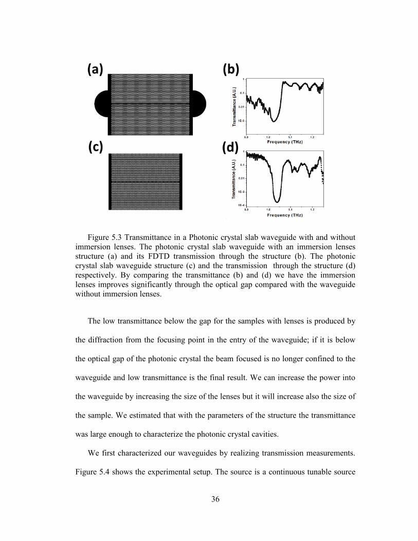
To estimate the effect of the immersion lenses in the transmission we realize
FDTD simulation of the whole structure. Figure 5.3(a) shows the calculation cell
used in a full 3D FDTD simulation for the waveguide with immersion lenses; the
figure corresponds to a plane centered in the middle of the slab. The corresponding
theoretical transmittance for the waveguide with immersion lenses is reported in
Figure 5.3(b). The structure for the waveguide without the immersion lenses and it
corresponding transmittance are shown in Figure 5.3(c) and Figure 5.3(d)
respectively.
From the FDTD simulation we have that the transmittance increased by as much
as factor 10 for the structure without the immersion lenses. The reason is very
simple: we have that the spotsize, 2mm, is larger than the input of the waveguide ,
about 100 μm, for the present structures. On the other hand the immersion lenses are
about the same size of the spotsize. The factor of 10 comes from the bigger cross
section of the beam that the lenses are able to focus into the entry of the waveguide.
In figure 5.4(d) the lower frequency edge of optical gap is located at 1.03 THz
and is clearly visible in the spectrum. A high transmittance is observed below the
edge of the optical gap for the sample without lenses which is clearly not seen in the
waveguide with immersion lenses.
36
Figure 5.3 Transmittance in a Photonic crystal slab waveguide with and without
immersion lenses. The photonic crystal slab waveguide with an immersion lenses
structure (a) and its FDTD transmission through the structure (b). The photonic
crystal slab waveguide structure (c) and the transmission through the structure (d)
respectively. By comparing the transmittance (b) and (d) we have the immersion
lenses improves significantly through the optical gap compared with the waveguide
without immersion lenses.
The low transmittance below the gap for the samples with lenses is produced by
the diffraction from the focusing point in the entry of the waveguide; if it is below
the optical gap of the photonic crystal the beam focused is no longer confined to the
waveguide and low transmittance is the final result. We can increase the power into
the waveguide by increasing the size of the lenses but it will increase also the size of
the sample. We estimated that with the parameters of the structure the transmittance
was large enough to characterize the photonic crystal cavities.
We first characterized our waveguides by realizing transmission measurements.
Figure 5.4 shows the experimental setup. The source is a continuous tunable source

37
manufactured by Virginia Diodes inc., the source consists of a frequency
synthesizer with a frequency span from 13.3 to 15 GHz. This is followed by a
cascade of three frequency doublers and two frequency triplers. The final output is
tunable from 0.9576 to 1.08 THz in steps as small as 72 KHz. The output launches a
Gaussian beam with a 2mm beam diameter and 5μW average power. The sample is
put in front of the source output and held in position by a metal slit to block the light
which is not guided through the sample. Once the beam is transmitted through the
sample a pair of of-axis parabolic mirrors collects the light and focuses into a 4K
Silicon composite bolometer. A wire grid polarizer is located between the two
parabolic mirrors to select the appropriate polarization.
Figure 5.4 Transmission experimental setup.

38
Figure 5.5 Experimental data is shown and compared with the FDTD simulation
for t = 46 μm and t = 44 μm for the 80 μm sample.
Figure 5.6 Experimental data is shown and compared with the FDTD simulation
for t = 45.6 μm and t = 43.7 μm for the 76 μm sample.

39
The experimental transmittance measurements are reported in Figure
5.5(Figure 5.6) for the 80μm (76 μm) sample. We normalize the transmittance using
the spectrum of the source and scaled to set the maximum in the waveguide
transmission equal to one for each lattice constant.
The results for the samples with lattice constant 80 μm are shown in Figure
5.5. The waveguide starts transmitting at 1.015 THz. In Figure 5.6 we present the
transmittance for the sample with lattice constant a = 76 μm. We observe that the
edge of the transmission shifts to higher frequencies 1.053 THz as is expected for a
sample with a smaller lattice constant. The frequency position of the edge of the
transmission in both cases is less than 10 GHz, or within 1 % of the predicted value.
Figure 5.7 The Lorentzian filter formed by inserting a cavity in a photonic crystal
waveguide. The cavity consists of three holes missing along the J orientation in a
single mode photonic crystal slab with a triangular lattice of holes
The photonic crystal samples have the same dimensions as the waveguide
samples. The Lorentzian filter is formed by inserting the L3 cavity into the

40
waveguide and is delimited by two holes at each side of the cavity as is shown in
Figure 5.7.
The Lorentzian filters were also characterized using the same transmittance
setup. The transmittances for each lattice constant are shown in Figure 5.8 and
Figure 5.9. For comparison we have also plotted the transmittance for the waveguide
with the corresponding lattice constant.
Figure 5.8 Transmittance through the waveguide and the Lorentzian filter for the
sample with a=80 μm, a sharp resonance at 1.0296 THz in the Lorentzian filter, is
associated with the resonance mode of the L3 cavity.
We observe that for the sample with a=80 μm the transmittance for the
Lorentzian filters presents a sharp resonance at 1.0296 THz that corresponds to the
frequency of the cavity mode as shown in Figure 5.7. For the 76 μm shown in Figure
5.8 the transmittance has the cavity resonance shift to 1.0724 THz, again consistent
with the scalability property of photonic crystals.

41
Figure 5.9 Transmittance through the waveguide and the Lorentzian filter for the
sample with a=76 μm, a sharp resonance at 1.0724 THz in the Lorentzian filter, is
associated with the resonance mode of the L3 cavity.
The resonances for the Lorentzian filters are fitted using a Lorentzian line shape.
Figure 5.10 and Figure 5.11 shows the transmittance spectrum of the Lorentzian
filter. Here we normalize the transmission spectrum of the filter using the
transmission spectrum of the waveguide with the corresponding lattice constant.
For the sample with lattice constant 80 μm the resonance frequency is 1.0296
THz with a frequency width of 1.13 GHz which gives a Q value of 910 as shown in
Figure 5.10. The resonance frequency for the 76 μm sample is located at 1.0724 THz
with a frequency width 1.05 GHz or a Q value of 1020 as reported in Figure 5.11.

42
Figure 5.10 The transmittance through the filter is fit by a Lorentzian line center
at 1.0296 THz with Q=910 for the 80 μm sample.
Figure 5.11 The transmittance through the filter is fit by a Lorentzian line center
at 1.0724 THz with a Q=1020 for the 76 μm sample.
43
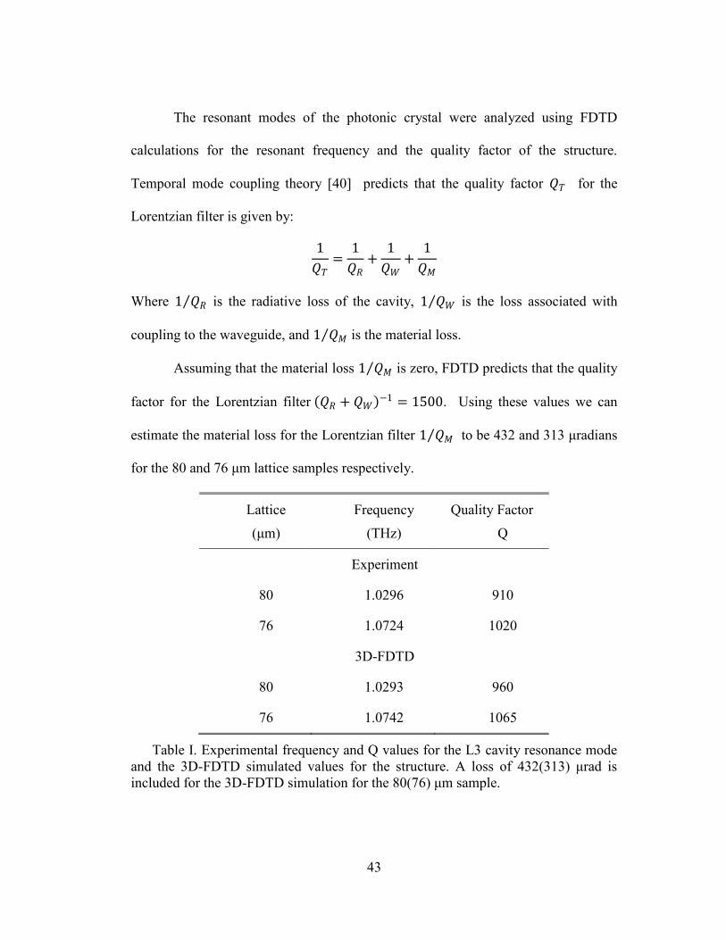
The resonant modes of the photonic crystal were analyzed using FDTD
calculations for the resonant frequency and the quality factor of the structure.
Temporal mode coupling theory [40] predicts that the quality factor 𝑄𝑇 for the
Lorentzian filter is given by:
1
𝑄𝑇=
1
𝑄𝑅+
1
𝑄𝑊+
1
𝑄𝑀
Where 1 𝑄𝑅 is the radiative loss of the cavity, 1 𝑄𝑊 is the loss associated with
coupling to the waveguide, and 1 𝑄𝑀 is the material loss.
Assuming that the material loss 1 𝑄𝑀 is zero, FDTD predicts that the quality
factor for the Lorentzian filter 𝑄𝑅 + 𝑄𝑊 −1 = 1500. Using these values we can
estimate the material loss for the Lorentzian filter 1 𝑄𝑀 to be 432 and 313 μradians
for the 80 and 76 μm lattice samples respectively.
Lattice
(μm)
Frequency
(THz)
Quality Factor
Q
Experiment
80 1.0296 910
76 1.0724 1020
3D-FDTD
80 1.0293 960
76 1.0742 1065
Table I. Experimental frequency and Q values for the L3 cavity resonance mode
and the 3D-FDTD simulated values for the structure. A loss of 432(313) μrad is
included for the 3D-FDTD simulation for the 80(76) μm sample.

44
As a consistency check, FDTD calculations where performed with the
estimated material losses, given a total Q value of 960 and 1065, which are close to
those found in the experiments (see Table I).
The absorption coefficient α can be calculated using the expression:
𝛼 =2𝜋𝑛𝑓
𝑐𝑇𝑎𝑛(𝛿)
Here we have that 𝑇𝑎𝑛(𝛿) is the loss tangent corresponding to the material
loss, 𝑓 is the frequency and 𝑐 is the velocity of light. With these values the
absorption coefficients are 0.318 and 0.240 cm-1
for the samples with 80 and 76 μm,
respectively. These values are higher than 0.01cm-1
, the reported value for intrinsic
absorption in high quality silicon with resistance higher than 10 kΩ-cm [32] . The
higher losses we observe indicate that our wafer has a lower resistivity than 10 kΩ-
cm (nominal resistivity 4 kΩ-cm) and there may also be small additional loss of
unknown origin.

45
6 Transversal Magnetic Photonic crystal cavity
In parallel to the fabrication and measurement of the TE photonic crystal slab
we also studied the possibility of the construction for a Transversal Magnetic (TM)
photonic crystal cavity. The search for a TM cavity is motivated by the fact that, for
some applications, a small resonant cavity with electric field normal to the surface of
a semiconductor wafer is desirable [17].
We employed FDTD to test different design until we finally chose the cavity
shown in Figure 6.1. The cavity consists in two holes missing along the ΓJ
orientation in a triangular lattice of air holes in a silicon slab. The cavity is
embedded in a waveguide and delimited by two holes at each side of the waveguide,
forming a Lorentzian filter. The characterization of these structure was done by
transmission and to enhance the coupling into the waveguide we used solid
immersion lenses that we incorporate into the structure [41].
Because of the fragility of this structure, which is only 21% Silicon in the
bulk of the photonic crystal, we chose a Si slab much thicker than the 50 µm slab
used in the TE samples discussed in the chapters 4 and 5. The slab supports several
transverse modes, up to five modes for the used thickness. High-Q cavity modes are
observed experimentally. The assignment of the experimentally-observed modes to
particular modes supported in the structure turned out to be significantly more
complicated than anticipated at the beginning of this project.
The work plan for this chapter starts with the fabrication of the samples and
the measure of the photonic crystal parameters. . We will start our measurements by

46
measuring the single most important feature of photonic crystal structure: its
photonic crystal gap because within where a photonic crystal cavity mode could be
found. The quality factor and frequency resonance of the cavity will we measure
through a high frequency resolution transmittance using a narrow band tunable
source. Then we will go through a heavy theoretical description of the cavity-
waveguide coupling, which ultimate goal is to indentify the resonant peak in the
transmittance as a resonant mode of the cavity. The identification process strongly
relies in the two dimensional picture of the cavity, i.e. the structure considering that
thickness is infinite, in which the identification of the modes is simpler. Employing
the symmetry set by the excitation pulse used in the experiment a single cavity mode
is positively identifies as the one observed in high frequency resolution transmittance
for the Lorentzian filter
A. Sample Fabrication
Figure 6.1 Optical photograph of the cavity embedded in the photonic crystal
waveguide. The lattice constant is a=135 μm, the thickness t=2.81 a and the hole
radius r=0.46 a.
47
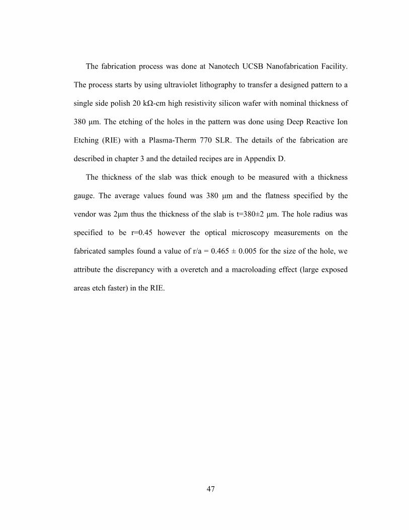
The fabrication process was done at Nanotech UCSB Nanofabrication Facility.
The process starts by using ultraviolet lithography to transfer a designed pattern to a
single side polish 20 kΩ-cm high resistivity silicon wafer with nominal thickness of
380 μm. The etching of the holes in the pattern was done using Deep Reactive Ion
Etching (RIE) with a Plasma-Therm 770 SLR. The details of the fabrication are
described in chapter 3 and the detailed recipes are in Appendix D.
The thickness of the slab was thick enough to be measured with a thickness
gauge. The average values found was 380 μm and the flatness specified by the
vendor was 2μm thus the thickness of the slab is t=380±2 μm. The hole radius was
specified to be r=0.45 however the optical microscopy measurements on the
fabricated samples found a value of r/a = 0.465 ± 0.005 for the size of the hole, we
attribute the discrepancy with a overetch and a macroloading effect (large exposed
areas etch faster) in the RIE.

48
B. Photonic crystal gap measurements
Figure 6.2 Terahertz time domain setup. A photoconductive switch is used as a
broadband source and it is detected by electro-optic effects using a ZnTe crystal and
balance photodiode bridge.
Our first step was to measure the photonic crystal gap of our strcutre; for this
purpose we employed a THZ-time-domain spectrometer (TDS); The THZ-TDS
system that we employed in the experiment has significant better signal to noise in 1
THz region compared with FTIR. THz-TDS technique relies on the fact that short
time pulses are formed by a large superposition of frequencies. The typical setup
consists in an ultra-short pulse typically around 100fs. The femtosecond pulse is
divided into two beams. One beam is used as a probe beam while the other is used to
excite an emitter. The emitter generates terahertz with bandwidth of a couple

49
terahertz depending of the generation scheme. In most conventional systems the
exciting beam before striking the emitter goes through a Michelson interferometer,
while the optical path of beam is kept fixed. Once the terahertz beam is generated it
goes through the sample and then is focused into a detector together with the probe
beam. The detector generates a signal that is a function of the electric field in the
terahertz beam. The probe pulse, being shorter that the Terahertz beam, maps the
electric field in the terahertz pulse as a function of the time delay of the excitation
pulse. This creates a time trace of the electric field that could be Fourier transform to
obtain the frequency information carried by the terahertz pulse.
Our THz-TDs system is based on a Ti:Sa laser with a photoconductive switch as
a source and detecting the signal through electro-optical. Single cycle terahertz
pulses were produced when 70 fs pulses with a wavelength of 800 nm from a A
Ti:Sa oscillator were delivered to a photoconductive switch. The femtosecond
pulse with energy above the bandgap generates carriers in the semiconductor
substrate. The carriers are then accelerated by a bias produced by a metal pattern in a
semiconductor substrate. The bandwidth of the produced Terahertz is determined by
the applied voltage and the pulse duration. In our setup as shown in Figure 6.2 the
switch consisted in an interdigitated structure [32] with a gap of 1.5 μm constructed
on a semi-insulating GaAs substrate. The bias voltage was set to 1.5 V which results
in an electric field of 10 kV/cm and the pulse energy of 2.5 nJ. With these values the
THz fields were a few tens of V/cm.

50
The beam was collimated and then refocused on to the sample with a spot size of
about 500 μm using off-axis parabolic mirrors (OAPMs). The transmitted pulse is
then analyzed by electro-optic detection in a 500 μm thick <110> oriented ZnTe
crystal and Lock-In detection to the frequency of the modulated bias voltage was
employed. The path of the THz radiation can efficiently be purged with dry nitrogen
to avoid water absorption. For the transmission, the TEM polarized THz pulses are
edge-coupled into the photonic crystal that was mounted in-between metal plates
without further focusing elements beside the OAPMs. The beam was focus in the
photonic crystal at a point locate around 2000 μm from the entry of the waveguide.
Although better coupling methods have been developed [42], the coupling efficiency
was large enough for our system.
In Figure 6.3 we show the time trace of the pulse traveling in the purged empty
box, a single cycle pulse is generated and it has a time width of a few picoseconds.
In Figure 6.4 we show the Fourier transform of the time trace. Here for the Fourier
analysis we only considering the time window before the second pulse is measured,
the second pulse is produces by the backside reflection inside the semiconductor
substrate.

51
Figure 6.3 Time domain trace of the reference
Figure 6.4 Fourier transform of the time domain trace.

52
From Figure 6.5 to Figure 6.7 we show the time domain trace and its
corresponding transmittance for samples with lattice constant 140, 135 and 150 μm
respectively; we use as a reference the transmittance of the single pulse in the empty
box shown in Figure 6.3 and Figure 6.4. For the three samples a large dispersion
from the single cycle reference is seen as is expected for a photonic crystal structure,
especially for the frequencies components that are close to the stop bands of the
structure where band dispersion in nearly flat.
Figure 6.5 Terahertz time domain measurement. Time trace of the Electric field
and THz pulse transmitted through the samples with lattice constant a=135 μm. A
low transmittance from 0.835 to 1.074 THz shows a good agreement with the FDTD
calculations.

53
Figure 6.6 Terahertz time domain measurement. Time trace of the Electric field
and THz pulse transmitted through the samples with lattice constant a=140 μm. A
low transmittance from 0.808 to 1.036 THz shows a good agreement with the FDTD
calculations.
Figure 6.5 to 6.7 shows a low transmittance region that is well matched by using
FDTD simulations of the structure which for the three figures are shown in solid
line. The values for the low transmittance predicted by FDTD and found are shown
in Table 6.1. The code used for calculating the transmittance in shown in Appendix
F.

54
Figure 6.7 Terahertz time domain measurement. Time trace of the Electric field
and THz pulse transmitted through the samples with lattice constant a=150 μm. A
low transmittance from 0.795 to 0.961 THz is consistent with the FDTD
calculations.

55
Lattice
constant
Start
frequency
End
frequency
Width
Gap to
midgap
(μm) (THz) (THz) (THz) (THz)
Experiment
150 0.795 0.961 0.166 0.189
140 0.809 1.036 0.227 0.246
135 0.835 1.074 0.239 0.251
3d FDTD
150 0.8265 0.9692 0.1427 0.1589
140 0.8754 1.0356 0.1602 0.168
135 0.9091 1.0877 0.1786 0.179
Table 6-1 Photonic crystal frequencies experimental and theoretical values, the
experimental error for the frequency is ± 10 GHz, corresponding to the resolution of
the THz-TDS
C. Photonic crystal gap theoretical calculation
The next step is to compare the transmittance with the theoretical model for the
photonic crystal. The thickness of the sample is several times the lattice constant and
therefore the slab is not single mode. In principle there is not a complete gap. We
will show that product of symmetry imposed by the THz beam used in our
experiment produces a low transmittance frequency region that for all practical
purposes works as an optical gap. This gap is the product of a stronger coupling to
the lower mode in the slab compared to the higher slab modes. We will base our
56
argument in symmetries and in fact we will verify by using FDTD to calculate the
transmittance through the photonic crystal as the ones shown in figure 6.5 to figure
6.7. We will show that the coupling higher modes of the modes slab are negligible.
1. Two dimensional calculation
Let start our analysis by considering the two dimensional (infinitely thick)
triangular photonic crystal. Figure 6.8 shows the band diagram calculated using
MPB; with the code shown in Appendix F. We show the Ez profile for several
points along the ΓJ direction in the triangular lattice. We have that band 1, 3 and 5
have their fields symmetric with respect to the ΓJ orientation and therefore could be
coupled to a plane wave (or any symmetric beam) traveling along this direction
while bands 2 and 4 with antisymmetric field do not couple to a plane wave. For a
symmetric in plane excitation we have that modes in bands 1, 3 and 5 will show a
transmittance, while modes in bands 2 and 4 will not.
From the band diagram we expect high transmittance up to 0.306, corresponding
to the first band. There is an optical gap from 0.306 to 0.484 (c/a), correspond to the
gap between band 1 and band 3. Then comes another small window of transmittance
from 0.484 to 0.520 (c/a), corresponding to band 3. These optical gaps are confirmed
by FDTD simulation as shown in Figure 6.9.
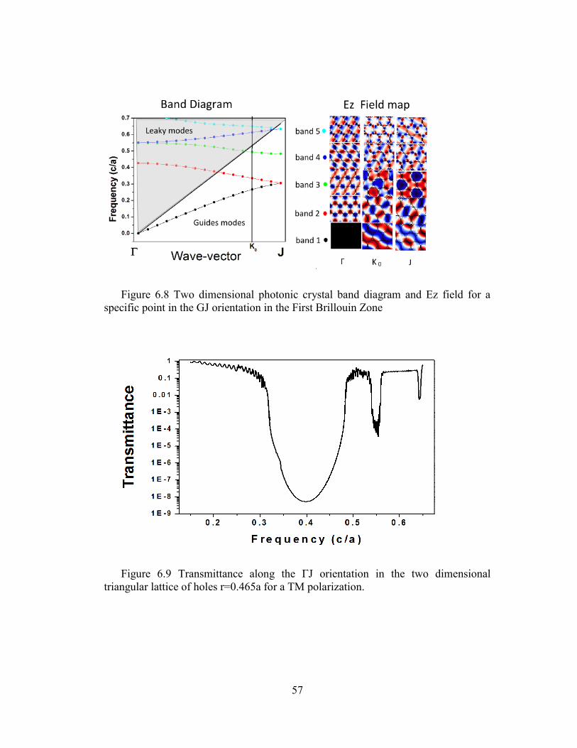
57
Figure 6.8 Two dimensional photonic crystal band diagram and Ez field for a
specific point in the GJ orientation in the First Brillouin Zone
Figure 6.9 Transmittance along the ΓJ orientation in the two dimensional
triangular lattice of holes r=0.465a for a TM polarization.

58
2. Three dimensional calculation
With the information obtained from the 2d case now we confront more easily the
highly more complicated band diagram of the 3d photonic slab structure. We realize
full 3D simulation of the photonic crystal slab using the parameters corresponding to
the 135 μm sample (the qualitative description will be the same for all the samples).
The code used is in Appendix F.
The band diagram for the finite thickness photonic crystal slab is shown in
Figure 6.10. Here we immediately notice the increase of the number bands in
comparison with two dimensional structures as a consequence of the finite thickness.
Figure 6.10 Three dimension Band diagram structure for the triangular lattice of
holes
Above the light line the modes are leaky i.e. they do not satisfy total internal
reflection and therefore are not guided through the slab; these modes are for our
purposes completely ignored.

59
Band # 1
Band #2
Band #3
Band #4
Band #5
Band #6
Band #7
Band #8
Band #9
Band #10
Band #11
Band #12
Band #13
Band #14
Band #15
Band #16
Figure 6.11 Ez field profile for the photonic crystal slab with thickness t=2.81a
and hole radius r=0.465a.

60
The modes below the light line are guided modes. In our experiment we excited
the system with a THz Gaussian beam; the symmetry imposed by the excitation
selects which modes are able to be excited and also the relative prominence of each
mode in the transmittance spectrum.
Our first selection rule is that modes which are not symmetric in the plane of the
slab will not be exited. This rule is the same as the two dimensional case in which
bands 3 and 4 in Figure 6.8 are not coupled.
Figure 6.12 Band diagram for the in plane symmetric modes. Below the light line
the modes are guided through the slab. Modes in the leaky region are not couple in
the transmittance and are omitted here.

61
The second rule is a quantitative estimate of the relative intensity when there are
more than one mode at the same frequency. This is a simple rule of thumb: the
higher the harmonic the weaker the coupling is; i.e. a mode which has a higher
number of nodes will couple weaker than a mode with a lower number nodes and
that the coupling strength is proportional to the overlap between the field of the
excitation beam and the field profile of the mode.
To explain this selection of a hierarchy of the modes we show the Ez field profile
at the J point in the Brillouin zone in Figure 6.11. The modes 1, 5, 7, 9, 10, 13, 14
and 16 are symmetric with respect to the ΓJ orientation and they could be exited in a
transmittance experiment. After eliminating the bands which are not symmetric and
keeping only the symmetric modes we have the band diagram show in Figure 6.12.
In Figure 6.12 we marked with ● (solid circle) the band which has a single node,
for example field mode in band 7 in Figure 6.11. These bands are the analogues for
the two dimensional case. These bands will be very strongly coupled by a Gaussian
beam, providing strong transmittance from 0 to 0.3195 (c/a) for the first one node
band and from 0.4899 to 0.5025 (c/a) for the second single node band.
Bands marked with a ■ (solid square) in Figure 6.12 are bands with three nodes
in the Ez field in the z direction, for example field mode in band 5 in Figure 6.11.
They have a lower coupling relative to the single node bands. We expect a low
transmittance when coupling to the modes in these bands. The three node bands
dominate the transmittance from 0.3195 to 0.40751 (c/a), and from 0.5328 to 0.5371.

62
Finally bands marked with ▲ in Figure 6.12 are band with modes with 5 nodes
in Ez field in the z directions, for example field mode in band 14 in Figure 6.11.
These bands have the lowest coupling of all the bands shown in Figure 6.12. They
dominate the transmittance where neither the single node nor the three nodes are
present. They are dominant from 0.4792 to 0.4899 (c/a), 0.5025 to 0.51585 (c/a) and
above 0.57831 (c/a).
We have that there is an optical gap in the symmetric modes from 0.40751 to
0.4792. Another small gap spans from 0.5371 to 0.57831. These gaps found from the
band diagram of the bright modes are confirmed by FDTD simulation of the
transmittance as shown in Figure 6.13.
Figure 6.13 (a) Band structure of the in plane symmetric modes (b) transmittance
along the ΓJ orientation.

63
The two dimensional model is extremely useful for understanding the
properties of the more complicated three dimensional slab. Our argument is that the
excitation beam selects the modes that we are able to couple and the lower modes
(modes with a single node in the Z direction) with a symmetric field along the
propagation direction are strongly dominant. If we just keep these single node modes
we have a description that matches very well the two dimensional case as shown in
Figure 6.14. However the match between the single node and the two dimensional is
not surprising since the three dimensional band structure should asymptotically
approximate to the two dimensional case as the slab increase it thickness. For the
present parameter the three dimensional bands structure for single node symmetric
modes are a few GHz higher that the corresponding two dimensional. The
approximation of using the two dimensional case for explaining the more complex
interaction between the THz beam and the 3D photonic crystal structure will be the
warhorse for analyzing the frequency response of the filter structure presented in the
present chapter.

64
Figure 6.14 Three dimensional bright modes compared with the two dimensional
photonic crystal band structures.
The optical transmittance found in the experiment allows working in the optical
gap which is in dimensionless frequency range of 0.40751 to 0.4792 (c/a). It is in
this frequency range where the resonant cavity modes are located.
D. Cavity mode measurements
Our purpose is to create a cavity with resonant frequency is the vicinity of 1THz
for transverse electric polarization. Once we have selected it we need a way to
characterize the cavity i.e. we want to know its resonant frequencies and its quality
factor. We need either to produce light inside the cavity or couple radiation into the
cavity. We use the later approach

65
For characterizing experimentally the resonant cavity of the photonic crystal we
inserted the cavity into a photonic crystal waveguide forming a narrow band
Lorentzian filter as shown in Figure 6.1. We expected that from this configuration
the peaks in the transmittance through the filter structure contained information on
the resonance frequency of the cavity and its quality factor.
Looking for resonant modes with high quality means narrow lines. For a quality
factor of 1000 at 1 THz for good characterization we require a frequency resolution
at least 0.1 GHz. This resolution is not accessible by using THz-TDS. However it is
easily obtained with our high resolution spectroscopy as shown in Figure 6.15.
The Terahertz spectroscopy setup shown in Figure 6.15 is based on a solid state
source made by Virginia Diodes inc., with a spectrum range from 0.9576 - 1.080
THz tunable in 72Khz steps. It outputs a polarized Gaussian beam with an average
power of 5 μW with a spot size of about 2 mm. The samples were located at the
output of the source and held in place by a metal plate. The output of the waveguide
then is focused into a 4k silicon composite bolometer using two off-axis parabolic
mirrors. A wire grid polarizer is positioned between the two parabolic mirrors to
select the polarization of the electric field normal to the plane of the slab (TM).

66
Figure 6.15 Terahertz frequency domain setup. A 0.957 to 1.080 narrow band
tunable source couples into sample. The signal is measured using a bolometer.
The transmittance is measured across the range of the source. The results are
shown in Figure 6.16. It’s worth mentioning that all the peaks that appear in the
spectrum are somehow a resonance of the cavity; among the peak that appear in the
spectrum we focus our attention on the isolate peak that appears around 0.99 THz for
the 140 and at 1.020 for the 135 µm sample. These peaks are well defined and
isolated from the rest which makes them more favorable for applications.

67
Figure 6.16 Frequency domain measurements for the Lorentzian filter. An
isolated peak (signaled with an arrow) well inside the region of low transmittance of
the photonic crystal is associated with a resonant mode for the cavity.(a) Here we
only observe a high transmission region near 0.960 GHz (b) A resonant mode at
located is 0.982 for the 140 μm sample. (c) A resonant mode is located at 1.020 for
the 135 μm sample.

68
To verify that the isolated peaks that appear in Figure 6.16 are resonant modes
we need to show that their frequencies and quality factors matches with the
theoretical predictions.
Figure 6.17 Frequency domain measurements for the Lorentzian filter in
dimensionless units. An isolated peak located at 0.46 (c/a) is observed for sample
with lattice constant a=140 μm and a=135 μm as shown in (b) and (c) respectively. A
high transmittance center at 0.48 (c/a) is observed for the three samples.

69
Our first step is to plot the data from Figure 6.12 using dimensionless units as
shown in Figure 6.13. We recognize that the features located at 0.48 (c/a) are similar
for the three samples; however these features are not the most interesting part of the
spectrum. The most significant feature is the lower frequency peak in the
transmittance within the stop band of the photonic crystal, which is associate with a
cavity resonant mode and is located at 0.982 (1.020) THz for the 140 (135) μm
sample. The transmittance also exhibits a high transmittance window, above
1.015(1.053) THz for the 140(135) μm sample, that corresponds to the upper edge of
stop band and in this region there are also several peaks corresponding to modes
which are pushed into the stop band by the cavity. These modes however have
smaller quality factors and are very close each other and to the band edge, making
these modes less useful than the more isolate lower frequency mode.
The location of the peaks in the transmittance for the filter with respect to the
stops bands are more clearly observed by comparing them to the THz-TDS
measurements of the photonic crystal.
Figure 6.18 shows the comparison of the broad band THZ-TDS of the photonic
crystal transmittance (solid line) and the narrow band frequency domain
transmittance (dotted line). For this sample with lattice constant a=150 μm we have
that the edge of the gap, measured by THZ-TDS, is located at 0.960 THz. This
feature is also observed in the frequency domain measurement.

70
Figure 6.18 Time domain and Frequency domain measurements for the 150 μm
sample. Here we have that the edge of the stop band located at 0.960 THz matches
with the high transmittance in the filter. Both measurements suggest that the edge is
located precisely at 0.960 THz or in dimensionless units at 0.48 (c/a).
Figure 6.19 also shows the edge of the optical gap shifted to higher frequency
and located at 1.030 measured by THz-TD (solid line) for the 140 μm sample; above
this frequency there is region of transmittance which is corroborated by the
frequency domain (dotted line); in the spectrum it is clear that the peak at 0.9824
THz in the transmittance for the filter is inside the optical gap; a unequivocal
signature of a cavity resonance.

71
Figure 6.19 Time domain and Frequency domain measurements for the 140 μm.
Here we have that the edge of the stop band located at 1.038 THz overlaps with a
high transmittance in the filter. However the peak located at 0.9824 is well inside the
low transmittance region of the photonic crystal.
Figure 6.20 shows the edge of the photonic gap shifted to 1.074 measured by
THz-TD (solid line) for the 135 μm sample; above this frequency there is region of
transmittance which is corroborated by the frequency domain (dotted line); in the
spectrum it is clear that the peak at 1.0209 THz in the transmittance for the filter is
inside the optical gap; again an unequivocal signature of a cavity resonance.

72
Figure 6.20 Time domain and Frequency domain measurements for the 135 μm.
Here we have that the edge of the stop band located at 1.074 THz overlaps with a
high transmittance in the filter. However the peak located at 1.0209 is well inside the
low transmittance region of the photonic crystal.
The peaks in the transmittance located well inside the optical gap for the
transmittance are the resonant modes for the cavity. For now we can fit them to a
Lorentzian line shape. Figure 6.21 shows the Lorentzian fit of the resonances found
by THz-FD. The fit reveals a resonant frequency at 0.9824 and a Q factor 1190 for
the 140 μm sample; while for the 135 μm the resonance is located at 1.0209 and it
has a Q factor of 1540.
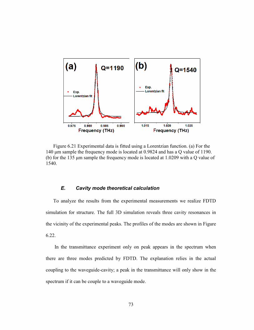
73
Figure 6.21 Experimental data is fitted using a Lorentzian function. (a) For the
140 μm sample the frequency mode is located at 0.9824 and has a Q value of 1190.
(b) for the 135 μm sample the frequency mode is located at 1.0209 with a Q value of
1540.
E. Cavity mode theoretical calculation
To analyze the results from the experimental measurements we realize FDTD
simulation for structure. The full 3D simulation reveals three cavity resonances in
the vicinity of the experimental peaks. The profiles of the modes are shown in Figure
6.22.
In the transmittance experiment only on peak appears in the spectrum when
there are three modes predicted by FDTD. The explanation relies in the actual
coupling to the waveguide-cavity; a peak in the transmittance will only show in the
spectrum if it can be couple to a waveguide mode.

74
Figure 6.22 The Ez field profile predicted by FDTD corresponding to three
resonant modes located near the resonant transmittance peak for the Lorentzian
filter. Figure (a) and (d) correspond to a cavity mode located at 0.4569 (c/a) with a
Q=6900; which correspond to a frequency 1.0153 (0.9791) for the 135(140) μm
sample. Figure (b) and (e) correspond to a cavity mode located at 0.46075 (c/a) with
a Q=1300 corresponding to 1.0239 (0.9873) THz for the 135(140) μm sample.
Figure (c) and (f) correspond to a cavity mode located at 0.46437 (c/a) with a
Q=1630; which correspond to 1.0319 (0.9951) THz for the 135(140) μm sample.
1. Two dimensional cavity modes
We need to discard two of the three modes. We start first by calculating the
waveguide modes for the more simple two dimensional photonic structure.
In the case of the triangular lattice we have that the translation symmetry
perpendicular to the slab (y-axis) is broken by the waveguide; however, we have that
it has discrete translation symmetry along the axis of the waveguide, as shown in
Figure 6.23. The modes for the waveguide could be divided in two main categories:
continuous extended bulk modes and discrete localized modes.

75
Continuous extended modes are modes propagating along the waveguide but not
exclusively bound to it; they extend into the bulk of the photonic crystal and
therefore they coupled to the bulk photonic crystal modes and as a consequence the
frequency spectrum for these modes is continuous.
Figure 6.23 In a photonic crystal waveguide the translation perpendicular to the
axis of the waveguide (y-axis) is broken; therefore the momentum in this direction is
not conserved. The translation symmetry along the axis of the waveguide (x-axis) is
still intact and therefore its momentum along this axis is conserved.
The second category will be the modes which are propagating and are localized
in the waveguide; therefore they are bounded and form a discrete set of frequencies.
In conclusion the dispersion relation of the waveguide will be a mix of continuous
extended bulk modes and a discrete set of localized modes
Our first step is to look for the bulk modes which are the photonic crystal modes
which have kx conserved or constant. These modes are characterized by a pair of
parameters frequency ω and propagating vector kx. A mode with ω and kx is a bulk

76
mode if there exists a ky such that ω= ω(kx, ky) is photonic crystal mode. In other
words we need to find the projection of the band diagram along the kx.
Figure 6.24 The projection of the band diagram of the photonic cyrstal slab as a
function of Kx. For a given Ko the frequency changes continuously from the
frequencies values determined by its intersection with the bands along the high
symmetric direction in the irreducible zone
The band projection along kx is the function ω =ω(kx). For constructing these
projection we first consider the point kx=k0 in the first Brillouin zone as shown in
Figure 6.24; the modes with a constant value of the kx are along the dotted line in
Figure 6.24(a). We know that the dispersion relation ω =ω(kx,ky) is only
discontinuous at the zone boundary, i.e. ω =ω(k0,ky) varies continuously from A to B
while covering the frequency interval 𝜔 𝐴 = 𝜔Γ𝐽 Γ𝐴 = 𝜔Γ𝐽 𝑘0 to 𝜔 𝐵 =
𝜔ΓX Γ𝐵 = 𝜔Γ𝑋 2𝑘0
3 ; There is also a continuous range of frequencies from the
point B to C which are the frequencies from 𝜔 𝐵 = 𝜔Γ𝑋 2𝑘0
3 to 𝜔 𝐶 =

77
𝜔Γ𝐽 ΓC = 𝜔Γ𝐽 2𝑘0 ; and finally also there are a continuous range of frequencies
from point C to D which are the frequencies from 𝜔 𝐶 = 𝜔Γ𝐽 2𝑘0 to 𝜔 𝐵 =
𝜔𝑋𝐽 𝑘0 ; where ωΓJ(k) is the band function along the ΓJ orientation, ωΓX(k) the band
function along the ΓX orientation and ωXJ(k) the band function along the XJ
orientation in the first Brillouin zone. We can define the following “projection”
functions in the interval 0 ≤ 𝑘 ≤ 𝜋𝑎 as:
𝑏1 𝑘 = 𝜔Γ𝐽 𝑘
𝑏2 𝑘 = 𝜔Γ𝑋
𝑘
cos(30°) = 𝜔Γ𝑋
2𝑘
3
𝑏3 𝑘 = 𝜔𝑋𝐽 𝑘 0 ≤ 𝑘 ≤
2𝜋
3𝑎
𝜔Γ𝐽 4𝜋
3𝑎− 𝑘
2𝜋
3𝑎 ≤ 𝑘 ≤
𝜋
𝑎
𝑏4 𝑘 =
𝜔Γ𝐽 𝑘
cos 60° = 𝜔Γ𝐽 2𝑘 0 ≤ 𝑘 ≤
2𝜋
3𝑎
𝜔𝑋𝐽 8𝜋
3𝑎− 2𝑘
2𝜋
3𝑎 ≤ 𝑘 ≤
𝜋
𝑎
(6.1)
We notice that if we consider k values larger that 𝜋/𝑎 the bands just flip their
order as they fold back into the Brillouin zone, providing the same range in
frequencies. The First Brillouin zone is symmetric so we only need to define the
projection function in the interval 0 ≤ 𝑘 ≤ 𝜋𝑎 .
In our case we are only dealing with modes that are symmetric along the
direction of propagation so we only consider band which are symmetric (see bands 1
3 and 5 in Figure 6.8). The gap in this particular case is delimited by band 1 and 3 so

78
only these two bands need to be considered. The projected bands function b1 to b4
define in equation 6.1 are plotted in Figure 6.25.
Figure 6.25 The projected band diagram over kx. Here b1 to b4 are the projected
function defined in equation 6.1. For a give kx we have that the frequency changes
continuously in k space from two consecutive intersections of the line with constant
value kx and the zone boundary.
Now that the extended bulk modes are obtained we are only left with the modes
which are bounded to the waveguide; to calculate the bounded modes we used
FDTD. These modes are obtained by exciting the waveguide with a pulse localized
at arbitrary points inside the waveguide as shown in Figure 6.26. For a given value
of kx we set the boundaries which are consistent with the Bloch function 𝑒−𝑖𝑘𝑥𝑥 .
And we let the system evolve in time. We monitor the field at various arbitraries

79
points inside the waveguide region and waveguide modes appear as resonant
frequencies of the cell structure.
Figure 6.26 The unit cell employed in the calculations of the waveguide modes;
the cell is excited by a broad pulse in an arbitrary point in the cell, the fields inside
are left to evolve subject to the boundary condition set by the Bloch function, the
resulting resonant frequencies are the eigenvalues for the particular Bloch function
employed.
In Figure 6.27 we show the localized modes for the waveguide, unsurprisingly
being localized they lie in the region of the photonic gap. For the two dimensional
structure that we are considering here there are 4 waveguide bands. The higher
frequency bands are pulled from the continuous states down into the optical gap. The
second higher frequency band is nearly flat. This particular band will have a very
slow group velocity. An interesting feature is also observed here: there is an
anticrossing between the two higher frequency bands; these bands in a bulk
dielectric will cross each other but in the photonic waveguide the discrete translation
symmetry produces a strong coupling between these two bands which produces this
anticrossing.
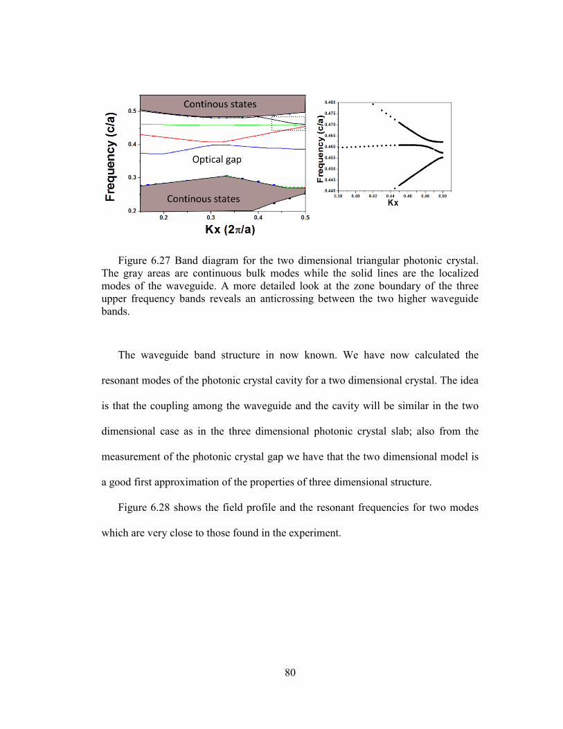
80
Figure 6.27 Band diagram for the two dimensional triangular photonic crystal.
The gray areas are continuous bulk modes while the solid lines are the localized
modes of the waveguide. A more detailed look at the zone boundary of the three
upper frequency bands reveals an anticrossing between the two higher waveguide
bands.
The waveguide band structure in now known. We have now calculated the
resonant modes of the photonic crystal cavity for a two dimensional crystal. The idea
is that the coupling among the waveguide and the cavity will be similar in the two
dimensional case as in the three dimensional photonic crystal slab; also from the
measurement of the photonic crystal gap we have that the two dimensional model is
a good first approximation of the properties of three dimensional structure.
Figure 6.28 shows the field profile and the resonant frequencies for two modes
which are very close to those found in the experiment.

81
Figure 6.28 The Ez field profile for two resonant modes of the two dimensional
photonic crystal cavities. (a) The resonant frequencies is located at 0.4527 (c/a) and
(b) the resonant frequency is located at 0.4601 (c/a).
The modes in Figure 6.28 have the same field configuration as modes (a) and (e)
in Figure 6.22 found in the three dimensional photonic crystal slab.
To qualitatively describe the coupling between the modes in Figure 6.28 we plot
the resonant frequency of the cavity in the waveguide band diagram. We examine
the Ez field profile in a few selected points in the waveguides. The points marked in
the dispersion relation as C and F show the field of the waveguide at the coupling
frequency. We see the field profile in C has a three nodes in y direction and a single
node in the x direction which matches very well the field configuration
corresponding to the modes shown in Figure 6.28(b). The mode profile for the
waveguide at point F, and in general the band that contains F, has a single node
while the field corresponding to the mode in Figure 6.28(a) has three nodes;
therefore the coupling is negligible.
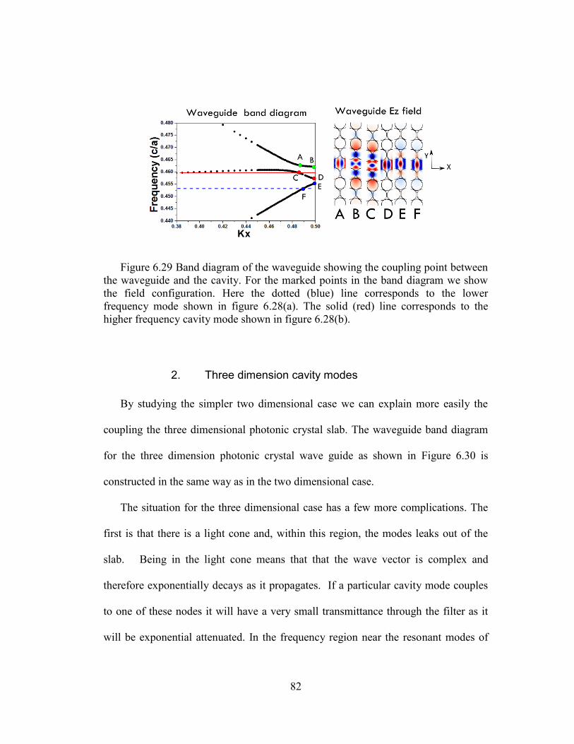
82
Figure 6.29 Band diagram of the waveguide showing the coupling point between
the waveguide and the cavity. For the marked points in the band diagram we show
the field configuration. Here the dotted (blue) line corresponds to the lower
frequency mode shown in figure 6.28(a). The solid (red) line corresponds to the
higher frequency cavity mode shown in figure 6.28(b).
2. Three dimension cavity modes
By studying the simpler two dimensional case we can explain more easily the
coupling the three dimensional photonic crystal slab. The waveguide band diagram
for the three dimension photonic crystal wave guide as shown in Figure 6.30 is
constructed in the same way as in the two dimensional case.
The situation for the three dimensional case has a few more complications. The
first is that there is a light cone and, within this region, the modes leaks out of the
slab. Being in the light cone means that that the wave vector is complex and
therefore exponentially decays as it propagates. If a particular cavity mode couples
to one of these nodes it will have a very small transmittance through the filter as it
will be exponential attenuated. In the frequency region near the resonant modes of

83
the cavity we have four band instead the three that appear in the two dimensional
case5.
Figure 6.30 Band diagram of the photonic crystal waveguide showing the
coupling point between the waveguide and the cavity. For the marked point the band
diagram we show the field configuration in the plane of the waveguide and also the
field across the thickness of the slab.
From the four waveguide bands that appear in Figure 6.30 three bands can be
associated directly to the two dimensional bands and they are the ones whose Ez
field has a single node in the z direction. The extra waveguide band is located in the
light cone and in the continuous states it has three nodes. By examining the field we
have that it is just a harmonic of the waveguide band that contains the point D in
Figure 6.30. Using the same argument that for the two dimensional case we can
discard the cavity mode corresponding to Figure 6.22(a) due to it having three nodes
while the waveguide to which it could couple only has one node. The cavity
corresponding to Figure 6.22(a) on the other hand can only strongly couple to the
5 In the two dimensional case, four bands appear but only three are in the vicinity
of the cavity resonances as is shown in Figure 6.29.

84
extra band with three nodes and is on the light cone therefore the coupling to this
particular mode will not show up in the transmittance spectrum.
After discarding two modes in Figure 6.22 we have that only one mode is able to
properly couple to the waveguide. This mode which corresponds to Figure 6.22(e)-
(f) is a cavity resonance mode appearing in the transmittance. Its frequency position
is at 1.0319 (0.9951) THz for the 135(140) μm with a quality factor Q=1630. We
have that by employing temporal coupled mode theory (Appendix C) the ratio of the
resonant frequency divided by the width of the resonant peak is the quality factor of
the cavity. We have that the Q factors found in the experiment are 1190 with a
resonant frequency of 0.9824 THz for the 140 μm sample and Q=1540 with resonant
frequency at 1.0209 for 135 μm sample. The departure from the perfect Lorentzian
line for the 135 μm sample could be explained as a result of the coupling in the
nearly flat region of the waveguide while the cavity in the 140 μm sample is located
a slightly smaller dimensionless frequency 0.4584 (c/a) compared to 0.4594 (c/a) for
the 135 μm and therefore in the linear region of the waveguide.
The discrepancy for frequency resonance between the experiment and the
theory is 10 GHz or 1% explained by an error in the FDTD or by small differences in
the parameters of the structure being simulated.

85
7 High-Q photonic crystal cavity for 0.24 THz
electron spin resonance.
In this chapter we move our attention to the sub THz regime where an intense
work has been done on characterizing complex system by using Electron Spin
Resonance (ESR) at 8.5 Tesla. ESR is a powerful technique in which a high Q low
volume cavity will enhance the sensitivity of the system, and therefore a motivation
for exploring the possibility of integrating a terahertz photonic crystal in a well
establish experimental technique.
The strategy we use for constructing a photonic crystal cavity at 0.24 THz
follows the trend from the previous chapter where an L3 cavity with a TE
polarization shows a cavity resonance as high as 1020 [41].
Using the property of scalability of photonic crystals for working at 0.24 THz we
only need to scale our samples properly. For a frequency of operation at 0.24 THz
we are required to construct our samples using a lattice constant of a=335 μm in a
190 μm thick wafer. The fabrication process is explained in chapter 3 and the
complete recipe is reported in appendix D.
We characterize our sample using a transmission experiment and scattering. For
the transmission experiment we use the setup shown in Figure 7.1. The THz source
is manufactured by Virginia diodes Inc. It consists of a frequency synthesizer that
covers the range from 14 to 16 GHz. It is then followed by four frequency doublers
multiplying the signal by 16 times to cover the range from 0.225 to 0.255 THz in

86
steps as small 16Hz. It has frequency dependent power ranging from 10 to
30mWwith the power around 240GHz approximately 20mW. The source launches a
Gaussian beam which at 240GHz has beam waist diameter of 5.6 mm.
Figure 7.1 Experimental setup. (a) Transmission configuration. (b) Scattering
configuration.
The source is mounted into a setup designed by Tomas Keating, Inc.; The source
is mounted on a 45 degree plate and it passed first through a wire grid polarizer
which is polarized also at 45 degree to match the polarization of the source. The
beam then passed through a 45 degree Faraday rotator to eliminate standing waves.
The beam emerges at the end with vertical polarization with respect to the optical
table. An off-axis parabolic mirror focuses the beam into a sample. Here any
reflection that comes from the sample will be rotated an additional 45 degrees and

87
will be cross polarized to the first wire grid and be taken out of the system
eliminating standing waves between the sample and the source.
A similar strategy is used for the detection. But this time the detection part of the
setup is mounted on a movable arm that can rotate 90 degrees. It consists on an off-
axis parabolic mirror which collects the light and then it goes to a wire grid polarizer
with axis perpendicular to the table. Then it goes to a 45 degree Faraday rotator and
is then detected with a Schottky diode which is polarization selective. This
configuration eliminated the standing waves formed either from the source to the
sample and from the sample to the detector. The configuration could be used in two
schemes: a direct transmission with the configuration shown in Figure 7.1(a) or by
measuring the scattering as shown in Figure 7.1(b).
Figure 7.2 Photonic crystal waveguide
Our first measurement was the characterization of a waveguide as shown in
Figure 7.2 . The waveguide is a linear defect along the TJ directions in the triangular

88
lattice. The dimension of the sample are 9 mm by 14 mm. The samples have an
immersion lenses for increasing the coupling from and into free space.
The spectrum of the photonic crystal waveguide is shown in Figure 7.3; we used
as a reference the source spectrum in free space. The spectrum shows a sharp
transmittance edge at 237 GHz. The waveguide has a sharp transmittance edge and
also a dip in the transmittance at 242.5 GHz.
Figure 7.3 Photonic crystal waveguide transmittance. The transmittance is
normalized using the spectrum of the source. At sharp transmittance turn on is
visible at 236 GHz while a dip in the transmittance is located at 242.5 GHz.
Once we now have a photonic crystal waveguide working in the desire frequency
range we proceed to construct a photonic crystal cavity. The sample design relies on
the L3 cavity, which is a cavity formed by removing three holes in the ΓJ orientation
in a triangular lattice. The L3 cavity was inserted into a photonic crystal waveguide

89
forming a structure known as Lorentzian filter. This structure is the same type that
one used in the two previous chapters. We have several samples that we can divide
in two main sets: The first set consists of three samples where we change the number
of holes that form the barriers which define the cavity in the waveguide from two to
four holes. The second set of samples consists of cavities with barriers consisting of
three holes where the hole closest to the cavity in the waveguide is shifted outward
enlarging the cavity as shown in Figure 7.4. The shifting of the inner hole tunes the
quality factor of the cavity. In particular Figure 7.5 shows a sample with three holes
as a barrier for the photonic crystal cavity. The dimensions for both sets of samples
are the same that were used for the waveguide, 9 mm by 14 mm. We also included a
pair of immersion lenses in each sample, enhancing the in/out coupling from free
space into the device.
Figure 7.4 The cavity quality factor of an isolated cavity (not coupled to any
waveguide) can be tuned by displacing the nearest hole to cavity outwards (a). The Q
factor changes as a function of displacement in (b), also a small change in frequency
is induced by the effective index of the cavity mode.

90
Figure 7.5 Photonic crystal Le cavity inserted into the waveguide. Here three
holes delimit the cavity in the waveguide forming a narrow band Lorentzian filter
The effective quality factor, i.e. the ratio of total energy stored to the energy lost
per cycle, in a photonic crystal could be written as:
1
𝑄=
1
𝑄𝑖𝑛+
1
𝑄𝑟+
1
𝑄𝑎𝑏𝑠+
1
𝑄𝑓𝑎𝑏 (7.1)
Here every term is associated with a different loss mechanism, Qin is the in plane
loss associated with the two dimensional photonic crystal, Qr is the radiative loss to
free space (also in the literature it is called QV or vertical loss), Qabs is the material
absorption and finally Qfab is the loss associated with surface roughness and in
general any deviation from the desired structure as a product of the fabrication
process. This last loss is negligible at terahertz frequencies due to the size of the

91
samples; however Qabs is the limiting factor at room temperature. At 240 GHz the
material loss is produced by free carrier absorption.
The in plane loss Qin could be made very large by increasing the length of the
crystal surrounding the cavity. In the case of our samples which are in the Lorentzian
filter scheme the in plane loss is dominated by the waveguide coupling.
The radiative or vertical loss could be minimized by carefully choosing the
design of the cavity. One way to increase Qr (i.e. decrease the radiative loss) was
first suggested by S. Noda et al [25]. They correctly addressed that by reducing the
abrupt discontinuity of the field inside the cavity i.e. by letting them penetrate inside
the dielectric mirror we are “gently confining” the fields, and so they do not
suddenly vanish at the interface and the leaky component are minimized.
The key to having a very effective mirror is periodicity. Therefore if we want to
make the mirror a little less reflective we only need to change the periodicity. There
are several ways to change the periodicity however the simplest way is just to move
the holes that are delimiting the cavity as shown in Figure 7.4.
Figure 7.4 shows the calculated quality factor and frequency for a cavity with a
thickness a=0.6 and hole radius r=0.30 for an index of refraction n=3.42 with a
lattice constant a=335 μm correspond to our samples. It is important to notice that
the highest quality is located around Δs=0.15a. We also notice a very small resonant
frequency shift to a lower frequency from Δs=0 to Δs=0.25. As we increase the size
of the cavity the effective index of refraction of the cavity in also increased, pushing

92
the mode to a lower frequency until it is large enough to be more energetically
favored for it to have an extra node.
To understand the effect of the holes displacements consider the field profile
corresponding to the resonant mode of cavity. Figure 7.6 (a) shown the Ey field
component and Figure 7.6(b) the Fourier components of the Ey field for the
unmodified cavity Δs=0.00. We clearly see that the modes are delocalized in the
Fourier space mostly confined in the X point, this modes extends weakly into the
leaky region. Being relatively small this cavity has an intrinsically high Q value.
Figure 7.6 (c) and Figure 7.6(d) shows the Ey field and its two dimensional Fourier
transform, again the mode is mostly confined in the X point in the reciprocal space
but now as a comparison with Figure 7.6(b) the leaky components are negligible and
therefore it has a higher Q value.
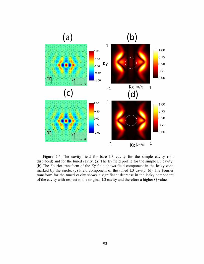
93
Figure 7.6 The cavity field for bare L3 cavity for the simple cavity (not
displaced) and for the tuned cavity. (a) The Ey field profile for the simple L3 cavity.
(b) The Fourier transform of the Ey field shows field component in the leaky zone
marked by the circle. (c) Field component of the tuned L3 cavity. (d) The Fourier
transform for the tuned cavity shows a significant decrease in the leaky component
of the cavity with respect to the original L3 cavity and therefore a higher Q value.

94
A. Photonic crystal resonance as a function of the length of
the barrier in a Lorentzian filter
Our first set of samples looks to increase the quality factor by increasing the in
plane quality factor which for the Lorentzian filter is dominated by the waveguide
coupling Q . We increase Q by adding more holes to form the barrier that set the
boundaries of the cavity inside the waveguide. We expect that as we increase the
number of holes the quality factor should also increase.
Figure 7.7(a) corresponds to a filter in which there are two holes delimiting the
cavity inside the waveguide. The spectrum shown a prominent peak located at
243.77 GHz which is associate with a cavity resonance. We clearly observe the edge
of the gap located at 231 GHz and also we have small transmittance from 238 to 240
GHz which is associated with the continuous states of the bulk photonic crystal. In
Figure 7.7(b) we show a close up into the resonance located at 243.77 GHz the
resonance could be fitted using a Lorentzian line. The quality factor associate with
the resonance line is Q=1313.
In Figure 7.7(c) we show the transmittance for the L3 cavity but this time the
cavity is delimited inside the waveguide by three holes. We observe in the
transmittance a resonant peak located at 243.36 GHz associate with a cavity
resonance, there is also a prominent peak at 252 GHz which correspond to a higher
frequency mode of the L3 cavity.

95
Figure 7.7 Transmittance through the filter for samples with two, three and four
hole barriers. For the sample with two and three holes a sharp resonance at a
frequency corresponding to a cavity mode is found. For the sample with four holes
no frequency was found that could be associated with a resonance. (a) and (b)
correspond to two hole barriers. (c) and (f) the transmittance for three hole barriers.
(e) Transmittance for the sample with a four hole barrier.
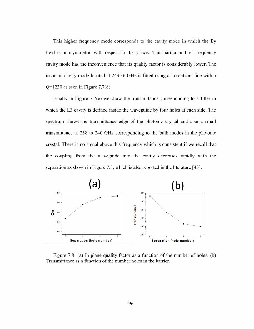
96
This higher frequency mode corresponds to the cavity mode in which the Ey
field is antisymmetric with respect to the y axis. This particular high frequency
cavity mode has the inconvenience that its quality factor is considerably lower. The
resonant cavity mode located at 243.36 GHz is fitted using a Lorentzian line with a
Q=1230 as seen in Figure 7.7(d).
Finally in Figure 7.7(e) we show the transmittance corresponding to a filter in
which the L3 cavity is defined inside the waveguide by four holes at each side. The
spectrum shows the transmittance edge of the photonic crystal and also a small
transmittance at 238 to 240 GHz corresponding to the bulk modes in the photonic
crystal. There is no signal above this frequency which is consistent if we recall that
the coupling from the waveguide into the cavity decreases rapidly with the
separation as shown in Figure 7.8, which is also reported in the literature [43].
Figure 7.8 (a) In plane quality factor as a function of the number of holes. (b)
Transmittance as a function of the number holes in the barrier.
97
Figure 7.8 shows Q as function of the number of holes and also the calculated
transmittance assuming no material absorption. We have that the transmittance
decreases dramatically from two to three holes and is very small for four holes which
agrees with the relative magnitude of transmittance as shown in Figure 7.7 (b) and
(c). We were expecting that the quality factor would increase; however, we clearly
see that it does not in the experiment. This particular issue is treated in more detail in
the next section.
B. Photonic crystal resonance as a function of the hole
displacement in the barrier for a Lorentzian filter
In section A we analyze the effect of the length of the barrier in the cavity
resonance. In the present section we will consider the effect of the hole displacement
in the frequency and quality factor of the cavity.
The set of samples that we are considering here are an L3 cavity with a three
hole barrier as shown in Figure 7.5 in which the inner hole in the barrier as shown in
Figure 7.4 is displace from its original position. The dependence of the resonant
frequency and the quality factor as a function of the hole displacement for a three
hole barrier is shown in Figure 7.9.

98
Figure 7.9 Quality factor and resonant frequency for the L3 cavity with a three
hole barrier inside a photonic crystal waveguide.
The experimental results for the 6 different samples are shown in Figure 7.10 and
in Figure 7.11 we show the detail of the peak in the transmittance that we associate
with the resonant mode of the cavity.
As we see in these measurements we have that the quality factor degrades as we
make the theoretical values of the cavity higher. This apparent discrepancy may be
solved if we consider the effects if non linear waveguide dispersion on coupling with
the cavity.

99
Figure 7.10 Transmittance through the filter for different displacement of the
inner hole of the cavity. (a) for Δs=0.00, (b) for Δs=0.05, (c) for Δs=0.10, (d) for
Δs=0.15, (e) for Δs=0.20 and (f) for Δs=0.25.

100
Figure 7.11 Lorentzian fit for the resonant peak found in the transmittance as a
function of inner hole displacement. (a) for Δs=0.00, (b) for Δs=0.05, (c) for
Δs=0.10, (d) for Δs=0.15, (e) for Δs=0.20 and (f) for Δs=0.25.

101
To understand the effect of the non-linear regime of the waveguide we shown in
Figure 7.12(a) the waveguide dispersion. Comparing to the cavity resonance in
Figure 7.9 we have that they are very close to the flat region of the waveguide. The
importance of being close to the flat region is that the coupling from the waveguide
into the cavity is roughly dependent of the inverse of the group velocity. The group
velocity is shown in Figure 7.12(b) although the calculation is more complicated
[44] we can extract a important piece of information from here, that the coupling is
very large for k vectors close to the zone boundary.
Figure 7.12 (a) Waveguide dispersion. (b) The coupling waveguide-cavity at first
approximation is proportional to inverse of the group velocity.
This is essential to explain the results from the transmittance. In the linear regime
of the waveguide the coupling factor is directly a factor multiplied by the group
velocity and therefore a constant. The response is a simple Lorentzian line. However
as shown in Figure 7.6(d), for a high Q cavity most of the components are near the
zone boundary and therefore the coupling at the points is higher. As a consequence

102
the Q factor is no longer the center frequency divided by the full width at half
maxima of the transmittance. In particular, the coupling for the higher quality factor
with its components in k space more confined at the zone boundary will be stronger.
As we can see the magnitude in the transmittance for the sample with Δs=0.15 is the
highest of all, which also correspond to a resonance with the larger frequency width,
a larger transmittance means a larger in plane coupling. Also in the transmittance
there is a small kink below the resonant peak, which is nothing else than the effect
that as the group velocity goes to zero, i.e. the density of state increases abruptly as
we approach to the zone boundary. This higher density of states allows the fields to
be evanescently couple from the input waveguide into the output waveguide and
gives us a good reference as to how far the resonant frequency is with respect to the
edge of waveguide.
In conclusion the cavity has a larger quality factor than the one that can be
inferred from the measurement.
We also did a scattering measurement, but also as we see in Figure 7.6(d) a high
quality cavity means that there is almost no component near the Γ point in the
Brillouin zone, which means that the radiation into free space will be nearly parallel
to the surface of the sample. Having in our setup a finite numerical aperture we
expect that the measurement of the scattering produced by the cavity will be very
small, as indeed we were only able to measure the scattering from two samples
which are shown in Figure 7.13.

103
Figure 7.13 (a) Full frequency range measurement of the light scattering by the
cavity for the sample with a two hole barrier. (b) Lorentzian fit for the cavity
resonance found for a two hole barrier. (c) Full frequency scan for the sample with a
three hole barrier and Δs=0.05. (d) Lorentzian fit for the cavity resonance found for
a three hole barrier and Δs=0.05.
We have that the shapes of the scattering out of the plane for the two samples that we
were able to measure are very symmetric and they are fit very well using a
Lorentzian line shape. We have that the values measured are considerably higher
than the ones obtained for the same sample in the transmission mode; also the
frequency is very slightly (less that 1/1000) shifted to higher frequency. The
essential difference with respect to the transmission mode is that while in

104
transmission there is a frequency cutoff in the transmittance. This cutoff is inexistent
for the radiation into free space and therefore the Q factor is directly the center
frequency dived by width of the Lorentzian line.
Thus we have that the sample with a three hole barrier with Δs=0.05 has a
quality factor of 3800. This is the highest measured for a photonic crystal cavity at
Terahertz frequencies, and is the highest quality factor measured at room
temperature\. The predicted quality factor for this is 6850 so that sets an estimated
loss of 1/3800-1/6850=117 μrad which is consistent with the values reported in
literature [45].

105
C. Photonic crystal resonances in the channel drop
configuration.
An alternative cavity-waveguide coupling scheme to the Lorentzian filter is the
channel drop configuration [25,46]. A cavity is located adjacent to the waveguide
and the evanescent field is coupled to the cavity as shown in Figure 7.14. The flux
through the waveguide shows a drop in its transmittance produce by the coupling to
the cavity, the magnitude of the drop is given by 𝑄 𝑄𝑟 2 where Qr is the radiative
loss and Q is the total quality factor of the cavity. The limitations present in the
Lorentzian filter, for which the transmittance becomes increasingly small as the
quality factor of the cavity is increased, are not present for the channel drop
coupling, since the in-plane quality factor Qω could be always be made comparable
to Qr and therefore Q and Qr are comparable.
Figure 7.14 Photonic crystal cavity in the channel drop configuration

106
We constructed two set of samples in the channel drop configuration. The cavity
was located two and three rows of holes from the waveguide. Figure 7.14 shows a
sample with three rows separation from the waveguide. For each separation distance
from the waveguide we fabricated six samples displacing the nearest hole in the
cavity as shown in Figure 7.4(a). The total size of the sample is 10X10 mm, with
3mm diameter immersion lenses to enhance the coupling between the sample and
free space.
The typical spectrum of a channel drop transmittance is shown in Figure 7.15.
The spectrum here was not normalized due to that the width of the drop is expected
to be very small since the transmittance does not change abruptly.
Figure 7.15 Typical transmittance for a Channel drop L3 cavity. A clear drop in
the transmittance is visible in the vicinity of 240 GHz.

107
The spectrum shows a clear turn on in the transmittance of the waveguide, with a
clear drop located in the vicinity of 240 GHz. The frequency width of the drop is
around 0.2 GHz. A detailed zoom of the transmittance is shown in Figure 7.16. Here
due to that the transmittance does not changes abruptly and the frequency width of
the drop is small, we can consider the reference transmittance to be a linear function.
By reference transmittance we mean the transmittance considering that the cavity is
decoupled from the waveguide. The ratio for the transmittance value in the deepest
point in the transmittance to the reference line is a measure of the coupling strength
of the cavity – waveguide system. From appendix C, we have that for the channel
drop scheme the magnitude of the drop is given by 𝑇1 𝑇0 = 𝑄 𝑄𝑟 2 . Here T1 is
the transmittance value in the deepest point in the drop; T0 is the value of the
reference line at the frequency corresponding to the deepest point in the drop, Q the
quality factor of the waveguide and Qr the radiative loss.
Figure 7.16 (a) A detailed zoom into the drop zone of the transmittance, the
reference line is the estimated transmittance if the cavity was decoupled from the
waveguide. The ratio of the transmittance with respect to the base line is a measure
of the coupling strength of the waveguide –cavity system. (b) Lorentzian fit of the
transmittance drop obtained by subtracting the drop signal from the reference line.

108
The drop into the waveguide is obtained by subtracting the drop signal from the
reference line in the transmittance as shown if Figure 7.16(a). The drop signal is then
fitted using a Lorentzian line and with the quality factor Q of the cavity given by
Q=ω0/Γ where Γ is the width at half maxima. This process is repeated for two set of
samples.

109
Figure 7.17 Transmittance of cavity waveguide coupled using the channel drop
configuration as a function of the inner hole displacement, the zone marks the
position of the drop. (a) for Δs=0.00, (b) for Δs=0.05, (c) for Δs=0.10, (d) for
Δs=0.15, (e) for Δs=0.20 and (f) for Δs=0.25.

110
Figure 7.18 Transmittance of cavity waveguide coupled using the channel drop
configuration as a function of the inner hole displacement. (a) for Δs=0.00, (b) for
Δs=0.05, (c) for Δs=0.10, (d) for Δs=0.15, (e) for Δs=0.20 and (f) for Δs=0.25.

111
The transmittance spectrum for channel drop samples with two and three row
separation as a function of the displacement of the nearest hole to the cavity are
shown in Figure 7.17 and Figure 7.18, The detailed characteristics of the
transmittances are reported in table 7.1.
Table 7.1 Experimental values for the cavity - waveguide coupled system in the
channel drop scheme. Here for sample with three holes and displacement Δs=0.10
and Δs=0.15 not clear drop is observed.
Δs fc (GHz) Δf (GHz) T1/T0 Q Qr
Two hole separation
0.00 239.608 0.2760 0.4103 868 1355
0.05 240.067 0.2121 0.2201 1132 2412
0.10 239.318 0.2030 0.3463 1179 2003
0.15 235.808 0.1601 0.0920 1473 4856
0.20 239.270 0.1849 0.2373 1294 2656
0.25 240.334 0.2562 0.2205 938 1997
Three hole separation
0.00 240.1027 0.3745 0.0705 641 2414
0.05 240.0605 0.2111 0.2619 1137 2428
0.10 N/O N/O N/O N/O N/O
0.15 N/O N/O N/O N/O N/O
0.20 236.528 0.1536 0.1250 1539 4355
0.25 240.623 0.29568 0.2664 813 1575

112
For the set of samples with two holes separation between the cavity and the
waveguide we observe a change in the quality factor of the cavity coupled to the
cavity and in the radiative quality factor, the trend is more clearly seen in Figure
7.19.
Figure 7.19 (a) Total quality factor of the L3 cavity in the channel drop
configuration as function of the inner hole. (b) Radiative quality factor as a function
of the displacement derived from the quality factor Q and the magnitude of the drop.
As we expected Figure 7.19(a) shows the quality factor of the structure should
increase with the displacement as it has a maximum between Δs=0.15 and Δs=0.20,
while the radiative quality factor also shows a peak for Δs=0.15 Figure 7.19(b).
For the set of samples with three rows separation we notice that we’re able
to observe a drop for all the samples except for two samples with three hole
separation and displacement Δs=0.10 and Δs=0.15. However the measured drops
reveals the same trend as I begin to increased from Δs=0.00 to Δs=0.10 and
decreased from Δs=0.20 to Δs=0.25.
To complement the transmittance measurement we also realized scattering
measurements. Again due that a high Q cavity has a radiation distribution nearly

113
parallel to the surface of the sample we were only able to measure few samples. The
measured samples are reported in Figure 7.20.
Figure 7.20 Transmittance and scattering measurements for the samples that we
we’re able to measure a scattering signal.(a) Two rows separation Δs=0.05. (b) Two
rows separation Δs=0.10. Two rows separation Δs=0.25. Three rows separation
Δs=0.05.
Figure 7.20 shows the scattering and the transmittance for the samples that we
were able to obtain a scattering signal from. We observe that the scattering signal
peaks where the transmittance has a drop as expected. The frequencies is slightly
higher in the scattering as it was also observed for the Lorentzian filter. This is
produced by the effect of the cavity resonance is very close to the non-linear regime

114
of the waveguide. The detailed spectrum near the peak in the scattering is shown in
Figure 7.21 .
Figure 7.21 Scattering peak and quality factor associated with the width of the
scattering peak for each sample where scattering signal was observed. (a) Two rows
separation Δs=0.05. (b) Two rows separation Δs=0.10. Two rows separation
Δs=0.25. Three rows separation Δs=0.05.
Figure 7.21 shows a very symmetric shape for the scattering in (a) and (d)
corresponding to Δs=0.05 for two and three rows. And the highest quality factor in
the channel drop is 2550. The non-symmetric shape in the scattering in (c) is
produced by the coupling in the non-linear regime and the shape of spectrum is
consisted with the estimated transmittance shape in this regime as is reported in
literature [44]

115
D. Summary for the 240 GHz cavities.
We have constructed and measured high Q cavities at 240 GHz. By tuning the L3
cavity it is possible to reach Q values as high as Q=3800 for the Lorentzian filter
coupling scheme as is measured with the scattering into free space by the cavity.
However the Lorentzian scheme is not well suited for the search for even higher Q
because the measurement depends of the amount of light coupled into the cavity and
because in-plane coupling decrease more rapidly than the total loss of the cavity, the
transmittance decreases very rapidly and therefore is very hard to measure.
The channel drop is more suited for measuring high Q cavity because, to have
and significant drop, we need to balance the coupling from the waveguide to the
radiative loss. For a given radiative loss we can always equal or at least have the
same order of magnitude loss by changing the distance between the cavity and the
waveguide.
We have that the quality factor calculated from the width of the transmittance in
both the Lorentzian filter and the channel drop could lead to errors if the cavity
resonance is very close to the flat region of the waveguide dispersion relation.

116
8 Conclusions
The experimental results reported in chapter 4 to 7 shows that indeed we
succeeded in constructing a high Q cavity that operates at Terahertz frequencies. At
1 THz we constructed and measured a photonic crystal cavity as high as Q=1020,
which compared with the metallic waveguide photonic crystal cavity with a Q≈100
provides a sharper resonance. We believe that the quality factor could reach higher Q
and at room temperature will be limited by the free carrier absorption.
A cavity with a Q=1020 will enable the strong coupling between shallow donors
in GaAs, therefore the next step has to be in the direction of fabricating the cavity
using GaAs instead of silicon. The processing of GaAs is slightly more difficult that
for silicon but it’s been already proven that high quality photonic crystal could be
constructed using reactive ion etching.
Also at 1 THz we constructed a transversal magnetic cavity intended to be
coupled to a quantum post with Q as high as 1560. The quality factor of the cavity
can be improved by carefully tuning the design of the cavity.
In the 240 GHz regime we also were able to obtain encouraging results by
constructing a cavity with quality factor near 4000, which is still below the value
needed for it to have a strong coupling to a spin ensemble; however, the
measurement was done at room temperature where the quality factor is severely
restricted by free carrier absorption, an inconvenience not present at low
temperature. Precisely, low temperatures are needed for it to be coupled to an
ensemble of spins because only a low temperature could the spins be properly

117
polarized. The cavity with a Q=4000 is however very promising for spin resonance
and we were looking to integrate this into the UCSB 240 ESR system.
The future path of work is work into reducing the insertion loss of the structure,
and also the waveguide needs to be modified in order to couple the cavity to the
linear dispersion of the waveguide. As we have shown in chapter 7 the cavities we
used are very close to the edge of the transmittance. To work in the linear dispersion
region the holes next to the waveguide need to be made smaller in order to increase
the effective index of the waveguide and therefore push to lower frequencies the
dispersion of the waveguide.
Photonic crystal structures are useful and very easy to integrate into more
complex devices and they are now one more tool available to the THz community
and science at large.

118
Appendix A. Eigen Value problem Maxwell equations.
In this appendix we will present the Maxwell equations for a lossless non
dispersive media as an eigenvalue problem.
The set of Maxwell equations without sources are:
∇ ∙ 𝐵 = 0 ; ∇ × 𝐸 +𝜕𝐵
𝜕𝑡= 0
∇ ∙ 𝐷 = 0 ; ∇ × 𝐻 −𝜕𝐷
𝜕𝑡= 0
(A.1)
If we consider that the displacement field (D) and induction field (B) are linear
function of the electric field E and magnetic field H. That the media is a non-
magnetic and the solutions for the fields are harmonic, i.e.:
𝐷 𝑟, 𝑡 = 휀0휀 𝑟 𝐸 𝑟, 𝑡 ; 𝐵 𝑟, 𝑡 = 𝜇 𝑟 𝐻(𝑟, 𝑡)
𝜇 𝑟 = 𝜇0
𝐸 𝑟, 𝑡 = 𝐸 𝑟 𝑒−𝑖𝜔𝑡 ; 𝐻 𝑟, 𝑡 = 𝐻(𝑟)𝑒−𝑖𝜔𝑡
(A.2)
We have that the set of Maxwell’s equations for the filed can be simplifies as:
∇ × 𝐸 − 𝑖𝜇0𝐻 = 0
∇ × 𝐻 + 𝑖𝜔휀0휀(𝑟)𝐸 = 0
(A.3)
From here its follows that:
𝐸 =𝑖
𝜔휀0휀(𝑟)∇ × 𝐻
∇ × 1
휀(𝑟)∇ × 𝐻 −
𝜔
𝑐
2
𝐻 = 0
(A.4)

119
Here we have that 𝑐 = 1 𝜇0휀0 . The equation for the magnetic field H, could be
formulated as a eigenvalue by defining an operator Ω as:
Ω𝐻 = ∇ × 1
휀(𝑟)∇ × H
(A.5)
is an hermitic vector field operator. With the above definition for Ω we have the
equation for H can be written as:
Ω𝐻 − 𝜔
𝑐
2
𝐻 = 0 (A.6)
Equation A.6 is denominated “Mater equation”; The solution of the master equation
that satisfies the transversality condition given by the divergence equation in A.1 are
the normal modes of systems.
In order to probe that Ω is a hermitic operator we first need a definition of the inner
product of two vector fields. We can use the canonical definition of inner product for
a vectorial space.
𝐴, 𝐵 ≝ 𝑑3𝑟 𝐴∗(𝑟) ∙ 𝐵(𝑟) (A.7)
Here A(r) and B(r) are three dimensional vector field and “ * ” denotes the complex
conjugate and “ . ” is the normal dot product for two vectors. In order to prove that Ω
is a Herminitan operator we need to prove that:
𝐴, Ω𝐵 = Ω𝐴, 𝐵 (A.8)
To verify this condition we only need to integrate by part twice:
𝐴, Ω𝐵 = 𝑑3𝑟𝐴∗ 𝑟 ∙ ∇ × 1
휀 𝑟 ∇ × 𝐵 𝑟
(A.9)

120
= 𝑑3𝑟 ∇ × 𝐴 𝑟 ∗∙
1
휀 𝑟 ∇ × 𝐵 𝑟
= 𝑑3𝑟 ∇ × 1
ε(r)∇ × 𝐴 𝑟
∗
∙ 𝐵 𝑟
= Ω𝐴, 𝐵
Here we neglect the surface terms of the integral because either the fields vanish at
the boundaries or they are periodical. In either case the surface integral vanishes at
the boundaries.
Because Ω is a Hermitian operator, it lets us reformulate Maxwell’s
equations for a lossless, non dispersive, non magnetic, linear media in the absence of
sources, into an eigenvalue problem for the magnetic field H. The different modes
obtained are orthogonal and they form a basis from which a general solution for the
Maxwell equations can be constructed.
The present eigenvalue formulation is based on the magnetic field and not in
the electric field, however once the solution for the magnetic field are known, the
electric field can be calculated using (A.4).

121
Appendix B. Bloch Theorem.
In this appendix we will present the photonic crystal concept. First we define the
translation operation in the crystal; and show the translation commutes by the
operator Ω defined in the master equation for the magnetic field H. We show that
the common solutions are indeed Bloch functions. Finally the concepts of band
diagram and reduce zone applied to photonic crystal are explain.
A crystal is a periodic structure. As any periodic structure it will repeated itself,
the length at which the structure is repeated is called lattice constant. For a three
dimensional crystal there are three independent orientation and therefore three
different repetition lengths. Let a1, a2 and a3 be three vector along each independent
orientation and be they magnitude the lattice constant along each orientation.
Lets know define the discrete translation operator as:
𝑇𝑅𝐴 𝑟 = 𝐴(𝑟 + 𝑅) (B.1)
Where R= la1 +pa2+qa3 , here l,p and are q integers; the eigenvalues of the
translation operator are 𝑒−𝑖𝑘∙𝑅 with k in a vector in the reciprocal lattice space.
From the concept of a crystal in which two points in the crystal are separated by
any integer linear combination of the lattice vectors are equivalent is natural to
consider that any operator that represents a physical quantity should be the same, i.e.
the operator representing a physics quantities must commute with the translation
operator.

122
In the language of operators if two operators commute it is possible to find a
common representation for both operators. In particular we are interested in the
operator defined by the master equation Ω; from its definition we know that because
휀(𝑟) is periodic the operator Ω will commute with the translation operator. To
actually prove that the translation operator TR commutes with the operator Ω we
apply it over an arbitrary field H(r).
𝑇𝑅Ω𝐻 𝑟 = 𝑇𝑅 ∇ ×1
휀(𝑟)∇ × 𝐻 𝑟 = 𝑇𝑅 ∇ ×
1
휀(𝑟)∇ × 𝐻 𝑟
= ∇R × 1
휀(𝑟 + 𝑅)∇R × 𝐻 𝑟 + 𝑅
= ∇ × 1
휀(𝑟)∇ × 𝐻 𝑟 + 𝑅 = ∇ ×
1
휀(𝑟)∇ × 𝐻 𝑟 + 𝑅
= Ω𝑇𝑅𝐻 𝑟
Since Ω and TR commute there hast to be a common set of eigenfuncions. Suppose
that H(r) is a common eigenfunction. The condition for H(r) to be an eingenfunction
of TR is:
𝑇𝑅𝐻 𝑟 = 𝐻 𝑟 + 𝑅 = 𝑒−𝑖𝑘𝑅𝐻 𝑟
We can define a function 𝑢 𝑟 = 𝑒−𝑖𝑘𝑟 𝐻(𝑟) ; and the easily prove that 𝑢 𝑟 is a
periodic function in R.
𝑢 𝑟 + 𝑅 = 𝑒−𝑖𝑘 𝑟+𝑅 𝐻 𝑟 + 𝑅 = 𝑒−𝑖𝑘𝑅 𝑒−𝑖𝑘𝑟 𝐻 𝑟 = 𝑒−𝑖𝑘𝑅𝑢 𝑟
With the periodicity of 𝑢 𝑟 we can write a final form for the Bloch theorem as:

123
𝐻𝑘 𝑟 = 𝑒𝑖𝑘𝑟 𝑢 𝑟 (B.2)
Here we are explicitly setting the k dependence in H. The solutions to the operator Ω
are planes waves modulated by a periodic function of the crystal; equation B.2 is the
Bloch theorem and its function are called Bloch waves.
Will be use the form of the Bloch function and substitute it inside the master
equation A.6.
Ω𝐻𝑘 𝑟 = 𝜔 𝑘
𝑐
2
𝐻𝑘 𝑟
Inserting the expression B.2 for Hk , and the definition of Ω we have that:
∇ ×1
휀(𝑟)∇ × 𝑒𝑖𝑘 ∙𝑟𝑢 𝑟 =
𝜔 𝑘
𝑐
2
𝑒𝑖𝑘 ∙𝑟𝑢 𝑟
By Applying the vector operations on the left side of the equation and by factoring
the exponential in both sides we have that the periodic function u(r) satisfies:
𝑖𝑘 + 𝛻 ×1
휀 𝑟 𝑖𝑘 + 𝛻 × 𝑢 𝑟 =
𝜔 𝑘
𝑐
2
𝑢 𝑟
Now defining the Hermitian operator Ωk as:
𝛺𝑘 𝑟 = 𝑖𝑘 + 𝛻 ×1
휀 𝑟 𝑖𝑘 + 𝛻 ×
(B.3)
The master equation for the periodic function u(r) is:
𝛺𝑘 𝑟 𝑢 𝑟 = 𝜔 𝑘
𝑐
2
𝑢 𝑟 (B.4)
By using the relation B.2, we find that the solutions of B.4 are the modes profile,
provided that they satisfy the tranversality condition inherited from A.2:

124
∇ ∙ 𝐻𝑘 = 0
This condition could be written in terms of u(r) as:
𝑖𝑘 + ∇ 𝑢 𝑟 = 0 (B.5)
A. Reduced Zone scheme
The functional form of the Bloch functions defined in B.2 does not put any
condition on k, however the periodicity of the function u(r) allows the restriction of
the range of the k vector to the first Brillouin zone.
Considering an arbitrary value of k, it is always possible to find a reciprocal
lattice vector G and a 𝑘′ vector in the first Brillouin zone such that:
𝑘 = 𝑘′ + 𝐺 (B.6)
The Bloch function Hk(r) associate with k satisfies the following equations:
𝐻𝑘 𝑟 = 𝑒𝑖𝑘𝑟 𝑢 𝑟
𝛺𝑘 𝑟 𝑢 𝑟 = 𝜔 𝑘
𝑐
2
𝑢 𝑟
Now let’s “fold” the k vector into the first Brilloin zone by using B.6:
𝐻𝑘 𝑟 = 𝑒𝑖𝑘𝑟 𝑢 𝑟 = 𝑒𝑖 𝑘 ′ +𝐺 𝑟𝑢 𝑟 = 𝑒𝑖𝑘′𝑟 𝑒𝑖𝐺𝑟𝑢 𝑟 = 𝑒𝑖𝑘′𝑟𝑢′ 𝑟
Where the function 𝑢′ 𝑟 defined as 𝑢′ 𝑟 ≡ 𝑒𝑖𝐺𝑟𝑢 𝑟 is a periodic function of the
lattice. This property follows from:
𝑢′ 𝑟 + 𝑅 = 𝑒𝑖𝐺 𝑟+𝑅 𝑢 𝑟 + 𝑅 = 𝑒𝑖𝐺𝑟𝑢 𝑟 = 𝑢′(𝑟)
Let’s apply the operator Ωk′ over 𝑢′(𝑟) using relation B.6 and the definition of
𝑢′(𝑟).

125
𝛺𝑘 ′ 𝑢′ = 𝛺𝑘−𝐺𝑒𝑖𝐺𝑟𝑢 = 𝑖 𝑘 − 𝐺 + 𝛻 × 1
휀 𝑖 𝑘 − 𝐺 + 𝛻 × 𝑒𝑖𝐺𝑟𝑢
= 𝑖 𝑘 − 𝐺 + 𝛻 × 1
휀 𝑖 𝑘 − 𝐺 × 𝑒𝑖𝐺𝑟𝑢 + 𝛻 × 𝑒𝑖𝐺𝑟𝑢
= 𝑖 𝑘 − 𝐺 + 𝛻 × 1
휀 𝑖 𝑘 − 𝐺 × 𝑒𝑖𝐺𝑟𝑢 + 𝑒𝑖𝐺𝑟 𝑖𝐺 + 𝛻 × 𝑢
= 𝑖 𝑘 − 𝐺 + 𝛻 × 𝑒𝑖𝐺𝑟 1
휀 𝑖𝑘 + 𝛻 × 𝑢
= 𝑖 𝑘 − 𝐺 × 𝑒𝑖𝐺𝑟 1
휀 𝑖𝑘 + 𝛻 × 𝑢 + 𝛻 × 𝑒𝑖𝐺𝑟
1
휀 𝑖𝑘 + 𝛻 × 𝑢
= 𝑖 𝑘 − 𝐺 × 𝑒𝑖𝐺𝑟 1
휀 𝑖𝑘 + 𝛻 × 𝑢 + 𝑖𝑒𝑖𝐺𝑟𝐺 ×
1
휀 𝑖𝑘 + 𝛻 × 𝑢
+ 𝑒𝑖𝐺𝑟𝛻 × 1
휀 𝑖𝑘 + 𝛻 × 𝑢 = 𝑒𝑖𝐺𝑟 𝑖𝑘 + 𝛻 ×
1
휀 𝑖𝑘 + 𝛻 × 𝑢
= 𝑒𝑖𝐺𝑟𝛺𝑘𝑢 = 𝑒𝑖𝐺𝑟 𝜔 𝑘
𝑐
2
𝑢 = 𝜔 𝑘′ + 𝐺
𝑐
2
𝑢′
From here we have that:
𝛺𝑘 ′ 𝑢′ 𝑟 = 𝜔 𝑘′ + 𝐺
𝑐
2
𝑢′ 𝑟 (B.7)
i.e. 𝑢′(𝑟) is solution of Ωk′ . From equations B.6 and B.7 we conclude that for any
arbitrary k vector exist a k’ in the first Brillouin zone such that the solution to Ωk is
also solution of Ωk′ . In conclusion the master equation B.4 only needs to be solved
inside the First Brillouin zone.
Equation B.7 also shows that there are a discrete number of eigenvalues for
the operator Ωk , by ordering the eigenvalues we can introduce n as an index to
distinguish between different modes for the same k value, therefore we can write the

126
frequencies solution as 𝜔𝑛𝑘 . The operator Ωk is a function of k and inside the first
Brillouin zone k can be varied continuously, therefore we can expect that 𝜔𝑛𝑘 also
to change continuous as a function of k.
It Is convenient to express the continuous variation of 𝜔𝑛𝑘 as a function of k
explicitly as 𝜔𝑛𝑘 = 𝜔𝑛 𝑘 . The set of functions 𝜔𝑛 𝑘 is called a band structure.
Figure B.1 The triangular lattice of holes; The reciprocal space with the first
three zones highlighted. The high symmetry points are shown and the detail of the
first Brillouin zone with its irreducible zone.
Figure B.1 shows the reciprocal space for the triangular lattice; the different
Brillouin zones and the high symmetric point are shown in the reciprocal space. The
underlying hexagonal symmetry is evident and it suggests that by rotating by 60
degrees and using plane symmetries the calculation space could be further shrink to

127
only consider the irreducible zone. The irreducible zone is the smallest set of k
vector with which rotations, reflections and inversions can reproduce the entire first
Brillouin zone and therefore the entire reciprocal space.
In this appendix we have found that photonic crystal modes are subject to the
proper symmetries of the crystal. The modes turns out to be Bloch functions which
are plane waves modulated by a periodic function of the lattice. A general solution
for the system is formed by a superposition of the Bloch modes, associated which
each Bloch function there is a k vector, which by the sole use of the translation
symmetries we only need to employ first Brillouin zone. Furthermore the use of
rotations and reflection reduces the problem to only solve for k vectors in the
irreducible zone.

128
Appendix C. Mode Couple Theory.
Couple mode theory is an approximation theory used to describe the interaction
in a complex system that can be broken down into simpler idealized components.
The solution to the overall systems is then expanded using the solutions or modes for
each component. The amplitudes of each modes will depend on the particular set of
rules obeyed by the overall systems, these rules will determine the couplings among
each component in the system.
A. Lorentzian Filter
We will apply couple mode theory to our particular case of a complex system
with a cavity and one or more waveguides. The localized modes for the cavity and
the propagating modes for the waveguide will be the components of the overall
system. The set of rules that the complex systems obeys are very general: Weak
coupling, energy conservation, time reversal invariance, time invariance and
linearity. The essential rule is weak coupling while the other four could be relaxed as
we will see.
We will first apply these ideas to the simple case of a filter. The filter consists of
an input waveguide through which the light is injected into the cavity, the cavity, and
the output waveguide that carries the filtered signal ( C.1).
In figure C.1 we have A proportional to the amplitude of the electromagnetic
field of the cavity mode, in general it is a complex quantity and is chose such that the
square of its magnitude (2
A ) is the energy stored in the cavity. S1,2± are the

129
complex quantities proportional to the propagating field in the waveguides such that
2
2,1 S are the energies fluxes. Here τ1,2 are the coupling factors between the cavity
and the waveguides.
Figure C.1 The Lorentzian filter system. The filter could break down into an input
and output waveguide coupled trough a cavity. Mode couple theory solves the
relation between the different scattering parameter and the coupling factor of the
waveguides to the cavity.
The temporal mode coupling theory equation for the field A in the cavity, with a
first order approximation, can be written as:
𝑑𝐴
𝑑𝑡= −𝑖𝜔0𝐴 −
𝐴
𝜏1−
𝐴
𝜏2+ 𝛼1𝑆1+ + 𝛼2𝑆2+
(C.1)
𝑆1,2− = 𝛽1,2𝑆1,2+ + 𝛾1,2𝐴 (C.2)
Here ω0 is the frequency mode of the cavity, α1,2 are the coupling factors from the
waveguide that is going into the cavity, β1,2 are the reflection coefficients produced

130
by the cavity and γ1,2 the coupling factor from the cavity into the waveguide. All
these quantities are not independents of each other.
To derive the relation among different couplings we first consider that there is
not incident flux going towards the cavity, i.e. S1,2+=0. The equation for the field A
in the cavity and the fluxes S1,2- are given by:
𝑑𝐴
𝑑𝑡= −𝑖𝜔0𝐴 −
𝐴
𝜏1−
𝐴
𝜏2
(C.3)
𝑆1− = 𝛾1𝐴 (C.4)
𝑆2− = 𝛾2𝐴 (C.5)
From C.3 it is straightforward to derive that:
𝑑𝐴∗𝐴
𝑑𝑡= −2
1
𝜏1+
1
𝜏2 𝐴∗𝐴
Here A* is the complex conjugate of the field amplitude in the cavity. The quality
factor is defined as 2π times the ratio of the time-average energy stored in the cavity
to the energy loss per cycle[ ref jackson]. As a result the quality factor is given by:
1
𝑄=
2
𝜔0
1
𝜏1+
1
𝜏2
(C.6)
Now consider the case where the right waveguide in figure C.1 is decoupled from
the cavity, i.e. 1 𝜏2 = 𝛾2 = 0 . Applying energy conservation we have that the
energy lost by the cavity is the energy of the flux moving out through the left
waveguide. So we have that:
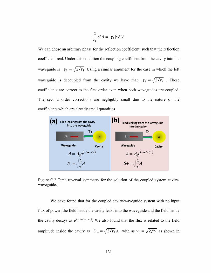
131
2
𝜏1𝐴∗𝐴 = 𝛾1
2𝐴∗𝐴
We can chose an arbitrary phase for the reflection coefficient, such that the reflection
coefficient real. Under this condition the coupling coefficient from the cavity into the
waveguide is 𝛾1 = 2 𝜏1 . Using a similar argument for the case in which the left
waveguide is decoupled from the cavity we have that 𝛾2 = 2 𝜏2 . These
coefficients are correct to the first order even when both waveguides are coupled.
The second order corrections are negligibly small due to the nature of the
coefficients which are already small quantities.
Figure C.2 Time reversal symmetry for the solution of the coupled system cavity-
waveguide.
We have found that for the coupled cavity-waveguide system with no input
flux of power, the field inside the cavity leaks into the waveguide and the field inside
the cavity decays as 𝑒(−𝑖𝜔𝑡−𝑡/𝜏). We also found that the flux is related to the field
amplitude inside the cavity as 𝑆1_ = 2 𝜏1 𝐴 with as 𝛾1 = 2 𝜏1 as shown in

132
figure C.2(a). If we apply the time reversal symmetry we find that for a flux coupling
from the waveguide into the cavity the field inside the cavity grows as 𝑒(−𝑖𝜔𝑡 +𝑡/𝜏)
and the field inside the cavity is related with the flux as 𝑆1+ = 2 𝜏1 𝐴 as shown in
figure C.2(b).
For this solution there is not output fluxes 𝑆1,2− = 0 and when this
conditions are inserted into equations C.1 and C.2 (here we decouple the right
waveguide) we find that:
𝑑𝐴
𝑑𝑡= −𝑖𝜔0𝐴 −
𝐴
𝜏1+ 𝛼1𝑆1+
(C.7)
0 = 𝛽1𝑆1+ + 𝛾1𝐴 (C.8)
From equation C.8 with the solution from the time reversal we have that:
𝑆1+ = −𝛾1
𝛽1𝐴 = −
2𝜏1
𝛽1𝐴 =
2
𝜏1𝐴
From the last equation we immediately find that 𝛽 = −1. Inserting the 𝑆1+ =
2 𝜏1 𝐴 into C.7 we have:
𝑑𝐴
𝑑𝑡= −𝑖𝜔0𝐴 −
𝐴
𝜏1+ 𝛼1
2
𝜏1𝐴
After some simple math we have that the change in energy of the cavity is given by:
𝑑𝐴∗𝐴
𝑑𝑡= −
2𝐴∗𝐴
𝜏1+ 2𝛼1
2
𝜏1𝐴∗𝐴
133
Energy conservation requires that this increase in the energy in the cavity to be equal
to the energy of the flux; we arrive to the following condition:
−2𝐴∗𝐴
𝜏1+ 2𝛼1
2
𝜏1𝐴∗𝐴 =
2
𝜏1𝐴∗𝐴
From the last equation we found that 𝛼 = 2
𝜏1; We can realize the same analysis for
the second waveguide and we will arrive to a similar results. Using the values found
for the different couplings we arrive to the mode coupling equations:
𝑑𝐴
𝑑𝑡= −𝑖𝜔0𝐴 −
𝐴
𝜏1−
𝐴
𝜏2+
2
𝜏1𝑆1+ +
2
𝜏1𝑆2+
(C.9)
𝑆1,2− = −𝑆1,2+ + 2
𝜏1,2𝐴
(C.10)
Let now analyze how the frequency filtering works. In a filter’s normal operation
we have an incident signal that travels through the waveguide and then interacts with
the cavity. The signal could be formed by a single frequency wave or it could have
some frequency bandwidth. In either case only the frequencies component that lies in
a certain frequency width around a cavity resonant mode are able to couple into the
cavity; the remaining frequency components will be strongly reflected. The signal
appearing in the output waveguide will therefore be filtered by showing only
frequencies that were able to couple into the cavity. The amplitude of the
transmission for each frequency component (frequency response) of the filter
depends on the filter structure. We will show that for the Lorentzian filter shown in

134
figure C.1 the frequency response is precisely a Lorentzian centered on the cavity
resonant and the width of the Lorentzian will correspond to the inverse of quality
factor of the cavity multiply by its resonant frequency.
We start with the couple mode theory equations C.9 and C.10 and considering
that for normal filter operation there is no input energy from the output (left
waveguide in figure C.1) waveguide, i.e 𝑆2+ = 0, and field amplitude inside the
cavity are harmonics, i.e. 𝐴(𝑡, 𝜔) = 𝐴𝑒−𝑖𝜔𝑡 , under these conditions we have that the
couple mode equations are:
−𝑖𝜔𝐴 = −𝑖𝜔0𝐴 −𝐴
𝜏1−
𝐴
𝜏2+
2
𝜏1𝑆1+
(C.11)
𝑆1− = −𝑆1+ + 2
𝜏1𝐴
(C.12)
𝑆2− = 2
𝜏2𝐴
(C.13)
From equation C.11 we have that:
𝑆1+ = 𝜏1
2 𝑖 𝜔0 − 𝜔 +
1
𝜏1+
1
𝜏2 𝐴
From the above equation the transmission coefficient is simple given by:
𝑇 𝜔 = 𝑆2−
𝑆1+
2
=
2𝜏2
𝜏1
2 𝑖 𝜔0 − 𝜔 +1𝜏1
+1𝜏2
2
=
4𝜏1𝜏2
𝜔0 − 𝜔 2 + 1𝜏1
+1𝜏2
2

135
Now using the definition for the quality factor C.6 the transmittance for a
symmetric case ( 𝜏 = 𝜏1 = 𝜏2 ) can be rewritten as:
𝑇 𝜔 =
14𝑄2
𝜔0 − 𝜔
𝜔0
2
+1
4𝑄2
(C.14)
This is a Lorentzian line center at the resonant frequency of the cavity. At
resonance we have that:
𝑇 𝜔0 = 1
Figure C.3 Illustration of the full width at half maxima for a transmittance curve.
The quality factor is given by the 𝑄 = 𝜔0 Γ ; where Γ is the full width at half
maxima of the transmittance curve and ω0 is the frequency resonant of the cavity in
this case the frequency corresponding to the peak in the transmittance.
The frequency width of the peak in the transmittance also includes important
information regarding the quality factor. The full width at half maxima (Γ) for the
transmittance (as illustrated in figure C.3) is defined as the frequency width of the

136
curve take at half the maximal value in the transmittance. At half maxima we
require that both terms in the denominator in equation C.9 to be equal. i.e.:
Γ
ω0=
1
𝑄
Which turns out to be what we expected that the width of the Lorentzian is the
inverse quality factor of the cavity times the resonant frequency. For the special
symmetric case in which the coupling to both waveguides are equal we have that the
transmittance at resonance is 100%.
The reflection coefficient is given by:
𝑅 𝜔 = 𝑆1−
𝑆1+
2
= −
𝜏1
2 𝑖 𝜔0 − 𝜔 +1𝜏1
+1𝜏2
+ 2𝜏2
𝜏1
2 𝑖 𝜔0 − 𝜔 +1𝜏1
+1𝜏2
2
= 𝑖 𝜔0 − 𝜔 +
1𝜏1
+1𝜏2
− 1
𝜏2𝜏2
𝑖 𝜔0 − 𝜔 +1𝜏1
+1𝜏2
2
= 𝜔0 − 𝜔 2 +
1𝜏1
−1𝜏2
2
𝜔0 − 𝜔 2 + 1𝜏1
+1𝜏2
2
Again for the symmetric case the reflection simplifies to:
𝑅 𝜔 = 𝜔0 − 𝜔
𝜔0
2
𝜔0 − 𝜔
𝜔0
2
+1
4𝑄2
With the result that the reflection vanishes at resonance. In conclusion for a
Lorentzian filter without losses the transmittance is a Lorentzian function whose
frequency width is the inverse of the quality factor times the resonant frequency of
the cavity and whose transmittance at resonance is 100%

137
B. Lorentzian Filter with losses
In a more realistic situation we have a Lorentzian filter which has external losses
such as radiative cavity losses and material absorption. We will focus on the former
effect due that radiative loss is intrinsic to the design of the cavity. Material losses in
principle are small6 and in can be incorporate to the calculation using the same
formalism.
Figure C.4 The Lorentzian filter with losses. The radiative loss is considered as
an extra decay mechanism for the radiation confined inside the cavity. In absence of
any other decay mechanism the quality factor of the cavity is given 𝑄 =𝜔0𝜏𝑟
2 this
factor is also called Q-radiative or Qr.
The schematics for a Lorentzian filter with loses is shown in figure C.4. The
coupled equations are simply modified from the Lorentzian filter without loss by
adding an extra channel for decay. For normal filtering operation we consider that
there is no input flux from the right, i.e. 𝑆2+ = 0. Under these conditions and
assuming harmonic fields the coupled equations are:
6 This is not true for Terahertz photonic crystal at room temperature due to
residual carrier absorption. However, this loss can be minimized by cooling down
the samples.

138
−𝑖𝜔 = −𝑖𝜔0𝐴 −𝐴
𝜏1−
𝐴
𝜏2−
𝐴
𝜏𝑟+
2
𝜏1𝑆1+
(C.15)
𝑆1− = −𝑆1+ + 2
𝜏1𝐴
(C.16)
𝑆2− = 2
𝜏2𝐴
(C.17)
The extra term in equation C.15 1 𝜏𝑟 is the radiative loss of the cavity and it
represents the field decay in the absence of all the other dissipation mechanisms. The
above equations are solved for the S parameter as a function of the field in the cavity
as follows:
𝑆1+ = 𝜏1
2 𝑖 𝜔0 − 𝜔 +
1
𝜏1+
1
𝜏2+
1
𝜏𝑟 𝐴
𝑆2− = 2
𝜏2𝐴
From here we have the transmission and reflection coefficients given by:
𝑇 𝜔 = 𝑆2−
𝑆1+
2
=
4𝜏1𝜏2
𝜔0 − 𝜔 2 + 1𝜏1
+1𝜏2
+1𝜏𝑟
2
𝑅 𝜔 = 𝑆1−
𝑆1+
2
= 𝜔0 − 𝜔 2 + −
1𝜏1
+1𝜏2
+1𝜏𝑟
2
𝜔0 − 𝜔 2 + 1𝜏1
+1𝜏2
+1𝜏𝑟
2

139
For a symmetric system we have that 𝜏𝜔 = 𝜏1 = 𝜏2 and defining QT, Qω and Qr
as:
1
𝑄𝑟=
2
𝜔0𝜏𝑟
1
𝑄𝜔=
4
𝜔0𝜏𝜔
1
𝑄𝑇=
1
𝑄𝜔+
1
𝑄𝑟=
4
𝜔0𝜏𝜔+
2
𝜔0𝜏𝑟
Here we have that QT is the quality factor of the cavity embedded in the
waveguide; for the coupled equation C.15 with not fluxes 𝑆1,2+ = 0 the field decays
with a decay constant given by:
1
𝜏=
2
𝜔0
2
𝜏𝜔+
1
𝜏𝑟
With the definitions of the partial quality factor the transmittance can be
rewritten as:
𝑇 𝜔 =
14𝑄𝜔
2
𝜔0 − 𝜔
𝜔0
2
+1
4𝑄𝑇2
(C.18)
𝑅 𝜔 = 𝜔0 − 𝜔
𝜔0
2
+1
4𝑄𝑟2
𝜔0 − 𝜔
𝜔0
2
+1
4𝑄𝑇2
(C.19)
We have that T(ω) for the Lorentzian filter with loss is also a Lorentzian line
and, we have that at resonance the transmittance is:

140
𝑇 𝜔0 =𝑄𝑇
2
𝑄𝜔2
The transmittance is not longer 100%. The full width at half maxima Γ requires that
the both terms in denominator in equation C.18 to be equal. Under this condition we
have that:
Γ
𝜔0=
1
𝑄𝑇
In conclusion we have that for a Lorentzian filter with losses the
transmittance is a Lorentzian line with a full width give by equation C.18 and
transmittance at resonance given by Eqn. C.18.

141
C. Channel drop configuration
The channel drop configuration for waveguide-cavity system in one where the
cavity is located next to the waveguide. Light traveling through the waveguide is
evanescently coupled into the cavity; the transmittance there will be a “drop” in the
signal with respect to a reference in which there is only a waveguide and no cavity.
From the drop of the signal and the width of the drop is possible to obtain the total
quality factor and the radiative quality factor of the cavity. The configuration for
this coupling scheme is shown in figure C.5.
Figure C.5 Channel drop configuration
For simplification here we consider that the system is symmetric and the
observation planes for the S parameter are located at the same distance from the
cavity. The first order coupled equations for the systems are the following.
𝑑𝐴
𝑑𝑡= −𝑖𝜔0𝐴 −
𝐴
𝜏𝜔−
𝐴
𝜏𝑟+ 𝛼1𝑆1+ + 𝛼2𝑆2+
(C.20)
𝑆1,2− = 𝛽1,2𝑆2,1+ − 𝛾1,2𝐴 (C.21)
𝑆𝑟 = 𝜅𝐴 (C.22)
142
By symmetry we have that β=β1=β2, α=α1=α2 and γ=γ1=γ2. Considering weak
coupling we have that α,γ, and 1/τ are small.
Our objective is to calculate the coupling factors α, β, and γ. To do this we first
consider a cavity that is decoupled from the waveguide. Thus we have that
1/τω=α=γ=0.
The coupled equation simplifies to:
𝑑𝐴
𝑑𝑡= −𝑖𝜔0𝐴 −
𝐴
𝜏𝑟
(C.23)
𝑆1,2− = 𝛽1,2𝑆2,1+ (C.24)
𝑆𝑟 = 𝜅𝐴 (C.25)
The energy conservation for systems require that energy leaking from the
cavity to be equal to the flux escaping from the cavity, i.e. it requires that:
−𝑑𝐴∗𝐴
𝑑𝑡=
2𝐴∗𝐴
𝜏𝑟= 𝜅 2𝐴∗𝐴 = 𝑆𝑟
2
The above equation is obtained by multiplying equation C.14 by A* and adding
the complex conjugated of the result. From here we derive that:
𝜅 = 2
𝜏𝑟
(C.26)
Also we have that the energy traveling to the waveguide is conserved therefore
we have that:
𝛽 = −1 (C.27)

143
Now lets consider that the coupling is weak and there is not input flux, i.e.
𝑆1,2+ = 0. The energy present in the cavity will decay into the waveguide and also
radiated out of the slab as shown in figure C.6(a).
Figure C.6 (a) Cavity decaying into the waveguide and frees space (b) Time
reversal solution, here the power in the cavity is increasing by in coupling radiation.
Here we have that the mode a couple equations reduce to:
𝑑𝐴
𝑑𝑡= −𝑖𝜔0𝐴 −
𝐴
𝜏𝜔−
𝐴
𝜏𝑟
(C.28)
𝑆1,2− = −𝛾𝐴 (C.29)
𝑆𝑟 = 𝜅 2
𝜏𝑟𝐴
(C.30)
144
Energy conservation requires that the energy lost by the cavity to be equal to the
flux leaking into the waveguide plus the energy leaking out of the slab. Thus energy
conservation requires:
−𝑑𝐴∗𝐴
𝑑𝑡= 2
1
𝜏𝜔+
1
𝜏𝑟 𝐴∗𝐴 = 2 𝛾 2𝐴∗𝐴 +
2
𝜏𝑟𝐴∗𝐴
From here we have that the coupling from the cavity into the waveguide is given by:
𝛾 = 1
𝜏𝜔
(C.31)
Finally lets use the time reversal symmetry as shown in figure C.6 (b). In this case
the direction of the flux is inverted i.e. 𝑆1,2− = 0, while the flux 𝑆𝑟 is now revered;
it’s energy is coupling from the exterior into the cavity. The corresponding time
reversal equations are:
−𝑑𝐴
𝑑𝑡= 𝑖𝜔0𝐴 −
𝐴
𝜏𝜔−
𝐴
𝜏𝑟− 𝛼𝑆1+ − 𝛼𝑆2+
(C.32)
0 = −𝑆2,1+ − 1
𝜏𝜔𝐴
(C.33)
−𝑆𝑟 = 2
𝜏𝑟𝐴
(C.34)
Energy conservation requires that the energy increase in the cavity to be equal to
the energy coming from the fluxes. However, since the fluxes 𝑆1+ and 𝑆2+ traveling
through the waveguide are equal in magnitude by symmetry and traveling in
opposed direction, these two fluxes cancel each other and, the net flux in then just
given by 𝑆𝑟 , from energy conservation we can derive that:

145
𝑑𝐴∗𝐴
𝑑𝑡= 2
1
𝜏𝜔+
1
𝜏𝑟 − 2𝛼
1
𝜏𝜔 𝐴∗𝐴 =
2
𝜏𝑟𝐴∗𝐴
From here we have that the coupling into the cavity is given by:
𝛼 = 1
𝜏𝜔
(C.35)
Finally the couple mode theory for the channel drop is given by:
𝑑𝐴
𝑑𝑡= −𝑖𝜔0𝐴 −
𝐴
𝜏𝜔−
𝐴
𝜏𝑟+
2
𝜏𝜔𝑆1+ +
2
𝜏𝜔𝑆2+
(C.36)
𝑆1,2− = 𝑆2,1+ − 2
𝜏𝜔𝐴
(C.37)
𝑆𝑟 = 2
𝜏𝑟𝐴
(C.38)
Now lets show how the filtering actually work. Consider figure C.5, for the
normal filtering operation we have that there is no input from the right, i.e 𝑆2+ = 0.
Considering a harmonic field in the cavity the couple mode equation C.26 and C.27
reduce to:
−𝑖𝜔 = −𝑖𝜔0𝐴 −𝐴
𝜏𝜔−
𝐴
𝜏𝑟+
1
𝜏𝜔𝑆1+
(C.39)
𝑆1− = − 1
𝜏𝜔𝐴
(C.40)

146
𝑆2− = 𝑆1+ − 1
𝜏𝜔𝐴
(C.41)
This system is easily solved, for 𝑆1−, 𝑆2− and 𝑆1+ as a function of A.
𝑆1+ = 𝜏𝜔 𝑖 𝜔 − 𝜔0 + 1
𝜏𝑟+
1
𝜏𝜔 𝐴
𝑆1− = − 1
𝜏𝜔𝐴
𝑆2− = 𝜏𝜔 𝑖 𝜔 − 𝜔0 +1
𝜏𝑟 𝐴
From here the transmittance and reflection coefficient can be written as:
𝑇 𝜔 = 𝑆2−
𝑆1+
2
= 𝜔 − 𝜔0
2 +1
𝜏𝑟2
𝜔 − 𝜔0 2 + 1𝜏𝑟
+1𝜏𝜔
2
(C.42)
𝑅 𝜔 = 𝑆2−
𝑆1+
2
=
1𝜏𝜔
2
𝜔 − 𝜔0 2 + 1𝜏𝑟
+1𝜏𝜔
2
(C.43)
We can define the quality factors as the following:
1
𝑄𝑟=
2
𝜔0𝜏𝑟
1
𝑄𝜔=
2
𝜔0𝜏𝜔
1
𝑄𝑇=
1
𝑄𝑟+
1
𝑄𝜔=
2
𝜔0𝜏𝑟+
2
𝜔0𝜏𝜔
The transmission and reflection coefficients can be rewritten as:

147
𝑇 𝜔 = 𝑆2−
𝑆1+
2
=
𝜔 − 𝜔0
𝜔0
2
+1
4𝑄𝑟2
𝜔 − 𝜔0
𝜔0
2
+1
4𝑄𝑇2
(C.44)
𝑅 𝜔 = 𝑆2−
𝑆1+
2
=
1
4𝑄𝜔2
𝜔 − 𝜔0
𝜔0
2
+1
4𝑄𝑇2
(C.45)
The transmittance given by equation C.44 corresponds to a Lorentzian drop with
respect to a reference line as shown in figure C.7.
Figure C.7 Channel drop transmittance spectrum.
We have that the Q of the cavity is obtained from the full width at half maxima
of the drop by 𝑄𝑇 = 𝜔0/Γ , and that at resonance we have that:
𝑇 𝜔0 = 𝑄𝑇
𝑄𝑟
2

148
The magnitude of the drop depends on the total QT factor of the cavity and Qr the
radiative quality factor. To have a significant drop we require both to be in same
order of magnitude. This is easily obtained even for very high QT since Q could be
increase faster than Qr by just increasing the distance between the waveguide and the
cavity. These represent an advantage over the Lorentzian filter since the magnitude
of peak in the transmittance involves the ratio of QT and Q in which the waveguide
coupling decrease more quickly that the radiative loss and therefore yields a very
low transmittance. In principle the channel drop scheme could be used to measure
very high Q cavities up to the point that material loss became important.

149
Appendix D. Fabrication recipes.
The fabrication process consists of a single lithography step following a reactive
ion etching. The photoresist used in the lithography is changed for the different
samples according to the thickness and the corresponding etching time.
A. Carrier wafer coating
This process is for the preparation of the carrier wafer used during the etching
process, for this purpose we use a silicon wafer with a thickness of around 500 μm.
For the wafer coating we use the Plasma Enhance Chemical Vapor Deposition
(PECVD) Plasma-Therm model 790 system. This system uses a capacitively-
coupled RF plasma source produced between two parallel aluminum plates. The
typical deposition rate is 400 A/min. at 300 mT pressure for a 250°C deposition.
[1] Wafer cleaning and drying takes two minutes in an ultra sound bath of
Acetone, Isopropanol and Methanol and DI water. Followed with N2 dry
and 5 minutes on the 110 C hot plate.
[2] PECVD clean and coating of the chamber takes 10 minutes at 250°C.
[3] PECVD deposition of 2 or 6 microns depending of the thickness of the
samples to construct.

150
B. Handling wafer preparation
For the construction of samples with a thickness of 50 μm, due to the fragility,
we used a handling wafer. For the thicker samples this step is omitted.
[1] We used a piece of silicon large enough for the samples and coated it
following the procedure for the carrier wafer. This piece of coated silicon
will be the handle wafer.
[2] We clean and dry for two minutes in a ultra sound bath of Acetone,
Isopropanol and Methanol and DI water. Followed with N2 dry and 5
minutes in the 110 C hot plate.
[3] Spin photoresist Az4110 on the handling wafer at 4k rpm for 30 seconds.
[4] Put the sample onto the handle wafer and apply uniform pressure on the
sample; I used a rectangular glass slide and a small weight (an empty
small bottle, two or three ounces in volume, used to storage small
quantities of photoresist).
[5] Bake for about 5 to 10 minutes on the 95°C hot plate will help the sample
stick to the handling wafer.
C. Lithography process
In this part of the process we use the handling wafer for the 50 μm thick samples
or just the wafer for the thicker samples. The specific process for each of the three
samples sets are:

151
1. TE photonic crystal samples 1 THz
[1] Cleaning and drying for two minutes in a ultra sound bath of Acetone,
Isopropanol and Methanol and DI water. Followed with N2 dry and 5
minutes in the 110 C hot plate.
[2] Spining the AZ4210 photoresist at 4k rpm for 30 seconds.
[3] Baking at 95°C for 60 seconds.
[4] Edge removal7.
[5] Expose for 15 seconds.
[6] Develop in Az400K diluted 1:4 for 70 seconds or until inspected under
the microscope that the features are clearly defined using a yellow light
filter.
2. TM photonic crystals sample 1 THz
[1] Cleaning and drying for two minutes in an ultra sound bath of Acetone,
Isopropanol and Methanol and DI water. Followed with N2 dry and 5
minutes in the 110 C hot plate.
[2] Due to the thickness of photoresist used for this set of samples we need to
promote adherence; so we spin the HDMS at 3500 rpm for 30 seconds
prior to the photoresist.
[3] Spin-on SPR220-7.0 resist at 3500 rpm for 45.
7 Edge removal is a optional step but in general leads to better results due to a
better contact between the sample and the photomask.

152
[4] Bake at 115°C for 120 seconds.
[5] Edge removal.
[6] Expose for 60 seconds.
[7] Wait for 5 minutes to complete the reaction.
[8] Develop MF701 for 70 seconds or until inspected under the microscope
the features are clearly defined using a yellow light.
3. TE photonic samples 240 GHz
[1] Cleaning and drying for two minutes in a ultra sound bath of Acetone,
Isopropanol and Methanol and DI water. Followed with N2 dry and 5
minutes in the 110 C hot plate.
[2] Spin AZ4330 photoresist at 4k rpm for 30 seconds.
[3] Bake at 95°C for 60 seconds.
[4] Edge removal.
[5] Expose for 20 seconds.
[6] Develop in Az400K diluted 1:4 for 90 seconds or until inspected under
the microscope the features are clearly defined using a yellow light.
D. Etching process
The etching was done using a Silicon Deep Reactive Ion Etching system (SiRIE)
Plasma-Therm 770 SLR. The system has an Inductively Coupled Plasma (ICP) coil

153
which also is coupled to an independent radio frequency supply (used to control the
generated plasma). This system is dedicated to deep etching in silicon and is
specially suited for the fabrication for Micro Electric Mechanical systems (MEMs).
In our case our samples has a range of thickness from 50 μm to 380 μm and this
systems produces high aspect ratio structures. The etching process consists of two
steps: First, a polymer deposition for passivation using C4F8 in which there is no
substrate bias, Second, is an etching cycle using a SF6 / Ar mixture with a substrate
bias.
We use Si02 coated silicon wafers as carrier wafers and photoresist patterned
samples. The etch rate of silicon and Si2 is 200:1 while the etch rate ratio of the
silicon photoresist is 80:1. The etch rate is highly dependent on the exposed silicon;
large open areas etches slower than small open area. Also high aspect ratio features
also etch slower than more open areas.
The first step of the process is a chamber clean out using a dedicated batch
process called season process. I usually use this step due to the recommendation of
the person in charge of the etcher. This process is recommended if the machine has
not been use in a couple of days. However it is recommended for consistency to have
the chamber in the same condition every time samples are processed. It is common
that more than one etch step is required however the cleaning only has to be done
once at the beginning and not between each etch process. The season process is
made with a blank silicon wafer.

154
Once the sample is ready for the etch process, it is mounted on the carrier wafer
which is coated with Si02, the sample can be glued to the carrier either using a thin
layer of photoresist or using Santovac. For convenience we used a few drop of
Santovac while applying pressure on the sample. Here it is important to make sure
that all excess oil is removed so that the wafer doesn’t get stuck to the robot arm or
inside the camber.
The time in the camber was calculated according to the thickness of the slab
using the nominal etch rate of 2 μm per minute. The 50 μm samples spend in the
chamber around 25 minutes. It could take up to several hours for the 380 μm samples
at the nominal etch rate (~190 minutes). Its recommend to divide this time in several
etch steps so the sample does not stay more than one hour inside the chamber. An
estimate of the etch rate could be done by estimating the depth of the etch using a
optical microscope because the etch rate in general is different from that of the
nominal rate. In our case, most of the samples had a slower etch rate.
E. Unmount of the wafers
This is the simplest but no less important part of the process. It is not uncommon
to break the sample at this the very last part of the process.
To remove the samples from the carrier wafer use Acetone and let it stays until it
can be easily slid out of the wafer. For the case of the thin wafer that was glued to a
handling wafer, an overnight bath in Acetone is needed. Cover the container with
Aluminum foil to avoid evaporation.

155
F. Edge removal
After the spinning step an excess of photoresist may accumulate on the edge of
the samples. This can produce make the sample stick to the photomask or just not
have a proper contact with the photomask, so is recommended to remove the edges.
Here we have two techniques that are commonly practiced:
Razor Blade
[1] Use a razor blade to scrape off resist from edges of the sample before
baking.
[2] Soft-bake resist as described in the particular recipe.
Overexpose and overdevelop
[1] Expose the sample 1 mm from its edge for 3 times the normal exposure
time. Use aluminum foil or any other material to block or absorb the UV
light. Develop using the corresponding developer for at least twice the
recommended time.
[2] Rinse with DI water and dry the sample with nitrogen.
[3] Inspect with the microscope using yellow light to verify the edge are
removed. If need it redo the process

156
Appendix E. Thin sample thickness measurement.
We estimate the thickness of the slab by measuring FTIR transmission normal to
the sample. We did this with either directly on sample in a region where there was no
photonic crystal structure or with a part of the wafer that was not processed. The
FTIR transmittance experiments were done in the near mid-infrared with a KBr
(Potassium Bromide) beam splitter using a DTGS (Deuterated Triglycine Sulfate)
detector.
Figure E.1 The Fabry-Pérot interference is shown in the transmission normal to
the wafer. The interference patters is a product of the finite thickness of the slab.

157
A typical transmission is shown in Figure E.1 where clearly resolved Fabry-Perot
interferences fringes are observed when they are compared with the spectrum of the
source. From the period of oscillation the thickness of the sample could be estimated.
A. Photonic crystal slab samples
Figure E.2 Normalized FTIR transmittance normal to the slab. (b) Linear fit of
the peak in the transmittance, the calculated slop δ=0.9043 THz which corresponds a
slab thickness of t=48.56 μm.
Figure E.2 (a) shows the normalized transmittance for the photonic crystal slab
used in chapter 4. In this transmittance we used as a reference the source spectrum
scaled by an arbitrary unit. The peak on the oscillation is linearly fit as shown in
Figure E.2(b). The thickness of the slab is computed from the slope of the lines

158
using the formula 𝑡 = 𝑐 2𝑛δ ; here n=3.416 is the index of refraction of Silicon in
the 1 THz region [47] and δ=0.9043 is the period of the oscillation (inverse of slop
of the line in Figure E.2 (b)). With these values we found the thickness is 𝑡 =
48.56 ± 0.03 𝜇𝑚.
B. High Q photonic crystal samples
Figure E.3 (a) Normalized FTIR transmittance normal to the slab. (b) Linear fit
of the peak in the transmittance, the calculated slop δ=0.9043 THz which correspond
a slab thickness of t=48.56 μm.
For the High Q photonic crystal cavity the transmittance perpendicular to the
slab in shown in Figure E.3(a), where clearly resolved Fabry-Perot oscillation are
observed. From the fit of the peak position as a function of the frequency in Figure

159
E.3(b), we found that the Fabry-Perot oscillations have a frequency period of
Δ𝑓 = 0.9999 ± 0.0004 THz. The corresponding thickness from the fit is 𝑡 =
43.83 ± 0.02. The thickness measurement was done in a single point measure in the
center of the wafer with a beam size of several millimeters. The flatness across the
wafer is specified by the manufacturer to be 2 μm so we estimate the thickness of the
wafer to be 𝑡 = 44 ± 2 μm.

160
Appendix F. MPB and MEEP files.
In the present appendix we show the files used for the simulation in thesis.
In each file we explain briefly the parameter that can be override by a command line.
There are several parameter that are common to all the structures, these parameters
are:
[1] r is the hole radius, for TE we used r=0.30 for TM we used r=0.465
[2] thick is the thickness of the slab; we used the dimensionless
experimental thickness, typically for TE t=0.6 and for TM t=2.80.
[3] eps is the value for the dielectric constant for silicon t=11.68.
[4] resolution is the number of point per unit cell, default value 32 for pc
band calculations, a value of 20 for TE cavity resonances and
transmittance for TE photonic crystal; and 32 for TM cavity and
transmittance for TM photonic crystals.
A. MPB : band diagram of a Photonic crystal
Here we present the code used for calculating the band diagram structure for a
photonic crystal.
1. Specific parameters:
[1] num-bands number of bands to calculate
[2] k-interp number of point between two high symmetric used in the band
diagram, the default value is 14.

161
[3] point optional parameter if only one point in the Brillouin Zone is
desired.
2. CTL file
band.ctl --------------------------------------------------------------------------------------------
; Triangular lattice of air holes in dielectric
; the parameter used for this simulations are
; first, define the lattice vectors and k-points for a triangular lattice:
(define-param sz 10)
(set! geometry-lattice (make lattice (size 1 1 sz)
(basis1 (/ (sqrt 3) 2) 0.5)
(basis2 (/ (sqrt 3) 2) -0.5)))
(define-param kz 0) ; use non-zero kz to consider vertical propagation
(set! k-points (list (vector3 0 0 kz) ; Gamma
(vector3 0 0.5 kz) ; M
(vector3 (/ -3) (/ 3) kz) ; K
(vector3 0 0 kz) ))
; For simulating the whole diagram Gamma-M-K-Gamma
; use the paramenter k-interp and interpolates between
; the high symmetric point
(define-param k-interp 14)
(set! k-points (interpolate k-interp k-points))
; For runnin at specific point not the whole diagram
; uncomment the following two expressions (and comment the two above)
(define-param point (vector 3 0 0 0))
(set! k-points (list point))
; Here we define the geometry:
(define-param eps 11.68) ; the dielectric constant of the background
(define-param r 0.30) ; the hole radius
(define-param thick 0.6); the thickness of the slab
(set! geometry (append
(list (make block (size infinity infinity thick) (center 0 0 0)(material (make
dielectric (epsilon eps) ))) )
(list (make cylinder (center 0) (material air)
(radius r) (height infinity)))))
; here are the resolution and number of bands for the simulation
(set-param! resolution 32)
(set-param! num-bands 16)
; here we select to run the te and tm bands if only one is desire
; comment the the other one.

162
(if (= kz 0)
(begin
(run-te)
(run-tm))
(run)) ; if kz != 0 there are no purely te and tm bands
End band.ctl ----------------------------------------------------------------------------------
3. Examples
[1] For calculating the band structure of a photonic crystal slab with a hole
radius r=0.30 and thickness 0.575.
mpb r=0.30 thick=0.575 band.ctl > band.out
[2] For calculating the band structure of a photonic crystal slab with a hole
radius r=0.465 and thickness 2.81.
mpb r=0.465 thick=2.81 band.ctl > band.out
B. MEEP: Waveguide dispersion relation
Here we present the code used for calculating the waveguide band diagram
structure for a photonic crystal. The strategy used to calculate the waveguide
dispersion, is to employ a pulse inside the optical gap of the photonic crystal
structure, and look for the resonances for the waveguide structure employing the
boundary conditions set by the Bloch function associate for each k vector from Γ to
the zone boundary.
1. Specific parameter
[1] fcen is the center frequency used for calculating the waveguide modes.
[2] df is the frequency width used for the excitation pulse.

163
[3] k-inter is the number of point to calculate the waveguide dispersion
relation from the Γ point to the boundary zone.
[4] point useful for running at a single reciprocal point.
2. CTL file
wgband.ctl ------------------------------------------------------------------------------------
; Some parameters to describe the geometry:
(reset-meep);
(define-param eps 11.682) ; dielectric constant of silicon
(define-param r 0.3) ; radius of holes
; The cell dimensions
(define-param sy (* 10 (sqrt 3)))
(define-param dpml 1) ; PML thickness
(define-param sx 1) ; size of cell in x direction
(define-param sz 5)
(define-param thick 0.575)
(define-param av false)
(set! eps-averaging? false)
(set! geometry-lattice (make lattice (size sx sy sz)))
(set-param! resolution 20)
; parameter of the excitation pulse
(define-param fcen 0.27) ; pulse center frequency
(define-param df 0.1) ; pulse width (in frequency)
; array used for containing the photonic crystal
(define pc (list ))
; pc geometry
;### center hole
(do ((j -4 (+ j 1))) (( > j 4))
(set! pc (append pc (list (make cylinder (center 0 (* j (sqrt 3)))(material air)
(radius r) (height thick) ) )) ))
;### side holes
(do ((j -4 (+ j 1))) ((> j 3))
(do ((i -1 (+ i 1))) ((> i 0 ))
(set! pc (append pc (list (make cylinder (center (+ i 0.5) (+ (/ (sqrt 3) 2) (* j (sqrt
3))))(material air) (radius r) (height thick) ) )) )))
;### covering the center hole
(set! pc (append pc (list (make cylinder (center 0 0 0)(material (make dielectric (epsilon eps)))
(radius r) (height thick) ) )) )
(set! geometry (append
(list (make block (center 0 0) (size infinity infinity thick) (material
(make dielectric (epsilon eps)))))
pc ))
(set! pml-layers
(list (make pml (direction Z) (thickness dpml))
(make pml (direction Y) (thickness dpml))))
; for TM band diagram use Ez instead of Hz
(set! sources (list
(make source
(src (make gaussian-src (frequency fcen) (fwidth df)))
(component Hz)
(center 0.123 0 0)

164
(size 0 0 thick))))
(set! symmetries
(list
(make mirror-sym (direction Y) (phase -1))
(make mirror-sym (direction Z) (phase 1))))
; use a output directory
(use-output-directory)
;For calculating the dispersion relation from the gamma point to the Brillouin edge
(define-param k-interp 24); iterpolation
(run-k-points 600 (interpolate k-interp (list (vector3 0 0 0) (vector3 0.5 0 0))))
; if only point is requiere commend the two above expression and uncoomment
; the next three commands, also change Hz by Ez for TM polarization
;(define-param point 0) ;Brillouin boundary
;(set-param! k-point (vector3 point 0 0))
;(run-sources+ 600 (harminv Hz (vector3 0.1234 0 0) fcen df)))
End wgband.ctl ------------------------------------------------------------------------------
3. Examples
[1] For calculating the waveguide band structure of a photonic crystal slab with a
hole radius r=0.30 and thickness 0.575; the waveguide dispersion is located
inside the gap near 0.27 (c/a).
meep r=0.30 thick=0.575 fcen=0.27 df=0.2 wgband.ctl > wgband.out
[2] For calculating the waveguide band structure of a photonic crystal slab with a
hole radius r=0.465 and thickness 2.81; the waveguide dispersion in
locateded inside the gap near 0.46 (c/a)
mpb r=0.465 thick=2.81 fcen=0.46 df=0.2 wgband.ctl > wgband.out
C. MEEP: Transmittance through the photonic crystal
Here we present the code used for calculating the transmittance through the
photonic crystal structure. We used several simulation using pulse with frequency

165
with a moderate frequency width instead doing a single simulation using a very
broad frequency single pulse.
user@pc: ~$ meep r=r0 thick=t eps=value resolution=value hds=disp l3cav.ctl > l3cav.out
1. Specific parameters
[1] fcen is the center frequency used for calculating the waveguide modes.
[2] df is the frequency width used for the excitation pulse.
[3] nfreq is the number of frequencies used for calculating the transmittance.
2. CTL files
trans.ctl ---------------------------------------------------------------------------------------
; Some parameters to describe the geometry:
(reset-meep);
(define-param eps 11.68) ; dielectric constant of waveguide
(define-param r 0.30) ; radius of holes
; The cell dimensions
(define-param sy (* 1 (sqrt 3))) ;
(define-param dpml 1) ; PML thickness
(define-param sx 30) ; size of cell in x direction
(define-param sz 5)
(define-param thick 0.6)
(define-param av false)
(set! eps-averaging? av)
(set! geometry-lattice (make lattice (size sx sy sz)))
(set-param! resolution 20)
;parameters of excitation pulse
(define-param fcen 0.27) ; pulse center frequency
(define-param df 0.1) ; pulse width (in frequency)
(define-param nfreq 1000) ; number of frequencies at which to compute flux
; extra parameter of the structure
(define-param nx 22) ; number of holes in the gamma-j orientation
(define pc (list )) ; array used in the photonic crystal
; geometry of the photonic crystal
; ### center hole
(do ((i (* -1 (/ nx 2)) (+ i 1))) ((> i (/ nx 2 )))
(set! pc (append pc (list (make cylinder (center i 0 0)(material air) (radius r) (height
thick) ) )) ))
;### side holes
(do ((i (* -1 (/ nx 2)) (+ i 1))) ((> i (- (/ nx 2 ) 1)))
(set! pc (append pc (list (make cylinder (center (+ i 0.5) (* -0.5 (sqrt 3)))(material air)
(radius r) (height thick) ) )) )
(set! pc (append pc (list (make cylinder (center (+ i 0.5) (* 0.5 (sqrt 3)))(material air)
(radius r) (height thick) ) )) ))

166
(set! geometry (append
(list (make block (center 0 0) (size infinity infinity thick) (material
(make dielectric (epsilon eps)))))
pc ))
(set! pml-layers
(list (make pml (direction X) (thickness dpml))
(make pml (direction Z) (thickness dpml))))
; used Ez if for TM photonic crystal
(set! sources (list
(make source
(src (make gaussian-src (frequency fcen) (fwidth df)))
(component Hz)
(center -13 0 0)
(size 0 sy thick))))
(set! symmetries
(list
(make mirror-sym (direction Y) (phase -1))
(make mirror-sym (direction Z) (phase 1))))
(define trans ; transmitted flux
(add-flux fcen df nfreq
(make flux-region
(center 13 0) (size 0 sy thick) )))
(use-output-directory)
(run-until 1000 )
(display-fluxes trans) ; print out the flux spectrum
End trans.ctl ---------------------------------------------------------------------------------
3. Examples
[1] For calculating the transmittance trough the photonic crystal. For the TE pc
with a hole radius r=0.30 and thickness 0.575; the transmittance between
0.20(c/a) to 0.3(c/a) is calculate using the following command.
meep r=0.30 thick=0.575 fcen=0.25 df=0.2 trans.ctl > trans.out
[2] For a TM photonic crystal slab with a hole radius r=0.465 and thickness 2.81;
the transmittance between 0.4(c/a) to 0.5 (c/a) is calculated using the
following command.
meep r=0.465 thick=2.81 fcen=0.45 df=0.2 trans.ctl > trans.out

167
D. MEEP: L3 Cavity resonance
Here we present the code used for calculating the resonant modes of the L3
cavity. The calculation can also include the material loss if desired. It also possible
to calculate the resonant mode for cavity in which the inner hole in the ΓJ orientation
next to the cavity is displaced from its original lattice position, this displacement
tunes the quality factor of the cavity.
1. Specific parameters
[1] fcen is the center frequency used for calculating the waveguide modes.
[2] df is the frequency width used for the excitation pulse.
[3] hds is the hole displacement from its original position, positive values
increase the size of the cavity.
[4] loss is the material loss that could be include in the calculation.
2. CTL file
l3cav.ctl---------------------------------------------------------------------------------------
; Some parameters to describe the geometry:
(reset-meep);
(define-param eps 11.68) ; dielectric constant of waveguide
(define-param r 0.30) ; radius of holes
; The cell dimensions
(define-param sy (* 11 (sqrt 3))) ; size of cell in y direction about 5 mm with a=80mu
(define-param dpml 1) ; PML thickness
(define-param sx 25) ; size of cell in x direction
(define-param sz 5)
(define-param thick 0.6)
(define-param av false)
(set! eps-averaging? av)
(define-param hds 0) ; hole displacement
(set! geometry-lattice (make lattice (size sx (+ sy 2) sz)))
(set-param! resolution 20)
; pulse excitation parameters
(define-param fcen 0.27) ; pulse center frequency
(define-param df 0.1) ; pulse width (in frequency)

168
; extra parameter used in the structure
(define-param nx 22); number of holes in the gamma-j orientation
(define pc (list )); array used for the pc structure
; In case of calculating the q factor with losses
(define-param loss 0)
(define-param fc fcen); center frequency for the loss (use the same value for fcen)
; geometry of the cavity
;### center holes in the strcutre
(do ((j -5 (+ j 1))) (( > j 5))
(do ((i (* -1 (/ nx 2)) (+ i 1))) ((> i (/ nx 2 )))
(set! pc (append pc (list (make cylinder (center i (* j (sqrt 3)))(material air)
(radius r) (height thick) ) )) )))
;### holes displaced in the unit cell
(do ((j -5 (+ j 1))) ((> j 4))
(do ((i (* -1 (/ nx 2)) (+ i 1))) ((> i (- (/ nx 2 ) 1)))
(set! pc (append pc (list (make cylinder (center (+ i 0.5) (+ (/ (sqrt 3) 2) (* j
(sqrt 3))))(material air) (radius r) (height thick) ) )) )))
;### covering the holes in the center of the structure
(do ((i -2 (+ i 1))) ((> i 2 ))
(set! pc (append pc (list (make cylinder (center i 0)(material (make medium (epsilon eps)
(D-conductivity (* 2 pi fc loss)))) (radius r) (height thick) ) )) ))
;### making the holed displaced from the orginal positions
(set! pc (append pc (list (make cylinder (center (- 0 2 hds) 0 0) (material air) (radius r)
(height thick) ) )) )
(set! pc (append pc (list (make cylinder (center (+ 2 hds) 0 0) (material air) (radius r)
(height thick) ) )) )
(set! geometry (append
(list (make block (center 0 0) (size infinity infinity thick) (material
(make medium (epsilon eps) (D-conductivity (* 2 pi fc loss)) ))))
pc ))
(set! pml-layers
(list (make pml (direction X) (thickness dpml))
(make pml (direction Z) (thickness dpml))
(make pml (direction Y) (thickness dpml))))
(set! sources (list
(make source
(src (make gaussian-src (frequency fcen) (fwidth df)))
(component Hz)
(center 0.5 0 0)
(size 0 0 0))
(make source
(src (make gaussian-src (frequency fcen) (fwidth df)))
(component Hz)
(center -0.5 0 0)
(size 0 0 0) (amplitude -1))
))
(set! symmetries
(list
(make mirror-sym (direction X) (phase 1))
(make mirror-sym (direction Y) (phase -1))
(make mirror-sym (direction Z) (phase 1))))
(use-output-directory)
(run-sources+ 1000
(after-sources
(harminv Hz (vector3 0.5 0 0) fcen df)
(harminv Hz (vector3 0.5 0.2 0.2) fcen df)))
End l3cav.ctl----------------------------------------------------------------------------------

169
3. Examples
[1] For calculating the cavity resonance of the L3 cavity with a hole radius
r=0.30 and thickness 0.6.
meep r=0.30 thick=0.6 fcen=0.27 df=0.2 l3cav.ctl > l3cav.out
[2] For calculating the L3 cavity with a hole radius r=0.3, thickness 0.575, with
loss 0.001 and the near hole displace by 0.05 a.
meep r=0.30 thick=0.575 fcen=0.27 df=0.2 hds=0.05 loss=0.001 l3cav.ctl > a.out
E. MEEP: L3 Lorentzian filter
Here we present the code used for calculating the resonant modes of the L3
cavity inserted into a photonic crystal waveguide to form a Lorentzian filter.
Material loss could be included and also the displacement of the inner hole
delimiting the cavity inside the waveguide.
1. Specific parameters
[1] fcen is the center frequency used for calculating the waveguide modes.
[2] df is the frequency width used for the excitation pulse.
[3] hds is the hole displacement from its original position, positive values
increase the size of the cavity.
[4] loss is the material loss that could be include in the calculation.

170
2. CTL file
l3filter.ctl ----------------------------------------------------------------------------
; Some parameters to describe the geometry:
(reset-meep);
(define-param eps 11.68) ; dielectric constant of waveguide
(define-param r 0.30) ; radius of holes
; The cell dimensions
(define-param sy (* 11 (sqrt 3))) ; size of cell in y direction about 5 mm with a=80mu
(define-param dpml 1) ; PML thickness
(define-param sx 25) ; size of cell in x direction
(define-param sz 5)
(define-param thick 0.6)
(define-param av false)
(set! eps-averaging? av)
(define-param hds 0) ; hole displacement
(set! geometry-lattice (make lattice (size sx (+ sy 2) sz)))
(set-param! resolution 20)
; pulse excitation parameters
(define-param fcen 0.27) ; pulse center frequency
(define-param df 0.1) ; pulse width (in frequency)
; extra parameter used in the structure
(define-param nx 22); number of holes in the gamma-j orientation
(define pc (list )); array used for the pc structure
; In case of calculating the q factor with losses
(define-param loss 0)
(define-param fc fcen); center frequency for the loss (use the same value for fcen)
; geometry of the cavity
(do ((j -5 (+ j 1))) (( > j 5))
(do ((i (* -1 (/ nx 2)) (+ i 1))) ((> i (/ nx 2 )))
(set! pc (append pc (list (make cylinder (center i (* j (sqrt 3)))(material air)
(radius r) (height thick) ) )) )))
(do ((j -5 (+ j 1))) ((> j 4))
(do ((i (* -1 (/ nx 2)) (+ i 1))) ((> i (- (/ nx 2 ) 1)))
(set! pc (append pc (list (make cylinder (center (+ i 0.5) (+ (/ (sqrt 3) 2) (* j
(sqrt 3))))(material air) (radius r) (height thick) ) )) )))
(do ((i (* -1 (/ nx 2)) (+ i 1))) ((> i (/ nx 2 )))
(set! pc (append pc (list (make cylinder (center i 0)(material (make medium (epsilon eps)
(D-conductivity (* 2 pi fc loss)))) (radius r) (height thick) ) )) ))
(set! pc (append pc (list (make cylinder (center (- 0 2 hds) 0 0) (material air) (radius r) (height thick) ) ))
)
(set! pc (append pc (list (make cylinder (center (+ 2 hds) 0 0) (material air) (radius r) (height thick) ) )) )
(set! pc (append pc (list (make cylinder (center 3 0 0) (material air) (radius r) (height thick) ))) )
(set! pc (append pc (list (make cylinder (center -3 0 0) (material air) (radius r) (height thick) ) )) )
(set! pc (append pc (list (make cylinder (center 4 0 0) (material air) (radius r) (height thick) ) )) )
(set! pc (append pc (list (make cylinder (center -4 0 0) (material air) (radius r) (height thick) ) )) )
; for four hole barrier unncomment the next two holes
;(set! pc (append pc (list (make cylinder (center 5 0 0) (material air) (radius r) (height thick) ) )) )
;(set! pc (append pc (list (make cylinder (center -5 0 0) (material air) (radius r) (height thick) ) )) )
; for five hole barrier unncomment the next two holes
;(set! pc (append pc (list (make cylinder (center 6 0 0) (material air) (radius r) (height thick) ) )) )
;(set! pc (append pc (list (make cylinder (center -6 0 0) (material air) (radius r) (height thick) ) )) )
; for six hole barrier unncomment the next two holes
;(set! pc (append pc (list (make cylinder (center 7 0 0) (material air) (radius r) (height thick) ) )) )
;(set! pc (append pc (list (make cylinder (center -7 0 0) (material air) (radius r) (height thick) ) )) )
(set! geometry (append
(list (make block (center 0 0) (size infinity infinity thick) (material
(make medium (epsilon eps) (D-conductivity (* 2 pi fc loss)) ))))
pc ))
(set! pml-layers

171
(list (make pml (direction X) (thickness dpml))
(make pml (direction Z) (thickness dpml))
(make pml (direction Y) (thickness dpml))))
(set! sources (list
(make source
(src (make gaussian-src (frequency fcen) (fwidth df)))
(component Hz)
(center 0.5 0 0)
(size 0 0 0))
(make source
(src (make gaussian-src (frequency fcen) (fwidth df)))
(component Hz)
(center -0.5 0 0)
(size 0 0 0) (amplitude -1))))
(set! symmetries
(list
(make mirror-sym (direction X) (phase 1))
(make mirror-sym (direction Y) (phase -1))
(make mirror-sym (direction Z) (phase 1))))
(use-output-directory)
(run-sources+ 1000
(after-sources
(harminv Hz (vector3 0.5 0 0) fcen df)
(harminv Hz (vector3 0.5 0.2 0.2) fcen df)))
End l3filter.ctl ----------------------------------------------------------------------
3. Examples
[1] For calculating the cavity resonance of the Lorentzian filter with a hole
radius r=0.30 and thickness 0.6.
meep r=0.30 thick=0.6 fcen=0.27 df=0.2 l3filter.ctl > l3filter.out
[2] For calculating the Lorentzian filter with a hole radius r=0.3, thickness
0.575, with loss 0.001 and the near hole displace by 0.05 a.
meep r=0.30 thick=0.575 fcen=0.27 df=0.2 hds=0.05 loss=0.001 l3filter.ctl > filter.out
F. MEEP: L2 Lorentzian filter
Here we present the code used for calculating the resonant modes of the L2
cavity inserted into a photonic crystal waveguide to form a Lorentzian filter.

172
1. Specific parameters
[1] fcen is the center frequency used for calculating the waveguide modes.
[2] df is the frequency width used for the excitation pulse.
2. CTL file
L2filter.ctl ---------------------------------------------------------------------------
; Some parameters to describe the geometry:
(reset-meep);
(define-param eps 11.682) ; dielectric constant of waveguide
(define-param r 0.46) ; radius of holes
; The cell dimensions
(define-param sy (* 10 (sqrt 3)))
(define-param dpml 1) ; PML thickness
(define-param sx 22) ; size of cell in x direction
(define-param sz 6)
(define-param thick 2.72)
(define-param av false)
(set! eps-averaging? av)
(set! geometry-lattice (make lattice (size sx sy sz)))
(set-param! resolution 32)
; excitation pulse parameters
(define-param fcen 0.5) ; pulse center frequency
(define-param df 0.2) ; pulse width (in frequency)
; extra parameters of the structure
(define pc (list )) ;array for the pc crystal
(define nx 18) ;number of holes along the gamma-j orientation
; L2 cavity geometry
;### center hole in the pc structure
(do ((j -4 (+ j 1))) (( > j 4))
(do ((i (* -1 (/ nx 2)) (+ i 1))) ((> i (+ 1 (/ nx 2 ))))
(set! pc (append pc (list (make cylinder (center (- i 0.5) (* j (sqrt 3)))(material
air) (radius r) (height thick) ) )) )))
;### side hole in the pc structure
(do ((j -4 (+ j 1))) ((> j 3))
(do ((i (* -1 (/ nx 2)) (+ i 1))) ((> i (/ nx 2 ) ))
(set! pc (append pc (list (make cylinder (center i (+ (/ (sqrt 3) 2) (* j (sqrt
3))))(material air) (radius r) (height thick) ) )) )))
;### covering the holes to form the waveguide
(do ((i (* -1 (/ nx 2)) (+ i 1))) ((> i (+ (/ nx 2 ) 1)))
(set! pc (append pc (list (make cylinder (center (- i 0.5) 0) (material (make dielectric
(epsilon eps))) (radius r) (height thick) ) )) ))
;### holes delimiting the cavity inside the waveguide (set! pc (append pc (list (make cylinder (center 1.5 0) (material air) (radius r) (height thick) ) )) )
(set! pc (append pc (list (make cylinder (center 2.5 0) (material air) (radius r) (height thick) ) )) )
(set! pc (append pc (list (make cylinder (center -1.5 0) (material air) (radius r) (height thick) ) )) )
(set! pc (append pc (list (make cylinder (center -2.5 0) (material air) (radius r) (height thick) ) )) )
(set! geometry (append
(list (make block (center 0 0) (size infinity infinity thick) (material
(make dielectric (epsilon eps)))))
pc ))
(set! pml-layers
(list (make pml (direction X) (thickness dpml))

173
(make pml (direction Z) (thickness dpml))
(make pml (direction Y) (thickness dpml))))
(set! sources (list
(make source
(src (make gaussian-src (frequency fcen) (fwidth df)))
(component Ez)
(center 0.5 0 0)
(size 0 0 thick))
(make source
(src (make gaussian-src (frequency fcen) (fwidth df)))
(component Ez)
(center -0.5 0 0)
(size 0 0 thick) (amplitude -1))))
(set! symmetries
(list
(make mirror-sym (direction X) (phase -1))
(make mirror-sym (direction Y) (phase 1))
(make mirror-sym (direction Z) (phase -1))))
(use-output-directory)
(run-sources+ 600
(after-sources
(harminv Ez (vector3 0.3 0 0) fcen df)
(harminv Ez (vector3 0.5 0 0) fcen df)
(harminv Ez (vector3 0.25 0.23 0.25) fcen df)))
3. Examples
[1] For calculating the cavity resonance of the Lorentzian filter with a hole
radius r=0.465 and thickness 2.81.
meep r=0.465 thick=0.2.8 fcen=0.46 df=0.1 L2filter.ctl > l2filter.out
G. MEEP: L3 Channel drop
Here we present the code used for calculating the resonant modes of the L3
cavity located next to the waveguide in the channel drop configuration. The
calculation include displacement of the inner hole delimiting the cavity inside the
waveguide and the distance from the waveguide
1. Specific parameters
[1] fcen is the center frequency used for calculating the waveguide modes.

174
[2] df is the frequency width used for the excitation pulse.
[3] hds is the hole displacement from its original position, positive values
increase the size of the cavity.
[4] lp is the distance from the waveguide; the default value is 0.5
corresponding to two line of holes. For three holes the value correspond
to lp=1.0, for four holes lp=1.5.
2. CTL file
cdrop.ctl -----------------------------
; Some parameters to describe the geometry:
(reset-meep);
(define-param eps 11.68) ; dielectric constant of waveguide
(define-param r 0.30) ; radius of holes
; The cell dimensions
(define-param sy 22) ; size of cell in y direction about 5 mm with a=80mu
(define-param dpml 1) ; PML thickness
(define-param sx 22) ; size of cell in x direction
(define-param sz 5)
(define-param thick 0.6)
(define-param av false)
(set! eps-averaging? av)
(set! geometry-lattice (make lattice (size sx sy sz)))
(set-param! resolution 20)
; pulse excitation parameters
(define-param fcen 0.27) ; pulse center frequency
(define-param df 0.1) ; pulse width (in frequency)
(define-param nx 22) ; number of holes along the gamma-j orientation
; extra parameters of the structure
(define pc (list ))
(define-param lp 0.5) ;two lines of holes separation
(define-param hds 0)
; geometry of the crystal
; center hole of the crystal
(do ((j -6 (+ j 1))) (( > j 6))
(do ((i (* -1 (/ nx 2)) (+ i 1))) ((> i (/ nx 2 )))
(set! pc (append pc (list (make cylinder (center i (* j (sqrt 3)))(material air)
(radius r) (height thick) ) )) )))
; displaced hole in the crystal
(do ((j 6 (+ j 1))) ((> j 5))
(do ((i (* -1 (/ nx 2)) (+ i 1))) ((> i (- (/ nx 2 ) 1)))
(set! pc (append pc (list (make cylinder (center (+ i 0.5) (+ (/ (sqrt 3) 2) (* j
(sqrt 3))))(material air) (radius r) (height thick) ) )) )))
; here we cover the holes to form the l3 cavity
(set! pc (append pc (list (make cylinder (center 0 (sqrt 3)) (material (make dielectric (epsilon
eps))) (radius r) (height thick) ) )) )
(set! pc (append pc (list (make cylinder (center -1 (sqrt 3)) (material (make dielectric
(epsilon eps))) (radius r) (height thick) ) )) )

175
(set! pc (append pc (list (make cylinder (center 1 (sqrt 3)) (material (make dielectric (epsilon
eps))) (radius r) (height thick) ) )) )
(set! pc (append pc (list (make cylinder (center -2 (sqrt 3)) (material (make dielectric
(epsilon eps))) (radius r) (height thick) ) )) )
(set! pc (append pc (list (make cylinder (center 2 (sqrt 3)) (material (make dielectric (epsilon
eps))) (radius r) (height thick) ) )) )
(set! pc (append pc (list (make cylinder (center (- 0 2 hds) (sqrt 3)) (material air) (radius r)
(height thick) ) )) )
(set! pc (append pc (list (make cylinder (center (+ 2 hds) (sqrt 3)) (material air) (radius r)
(height thick) ) )) )
; here we set the waveguide in the channel drop
(set! pc (append pc (list (make block (center 0 (* ( - 0 lp) (sqrt 3)) ) (material (make
dielectric (epsilon eps))) (size infinity 0.8 thick) )) ))
(set! geometry (append
(list (make block (center 0 0) (size infinity infinity thick) (material
(make dielectric (epsilon eps)))))
pc ))
(set! pml-layers
(list (make pml (direction X) (thickness (* 2 dpml)))
(make pml (direction Z) (thickness dpml))
(make pml (direction Y) (thickness (* 2 dpml)))))
(set! sources (list
(make source
(src (make gaussian-src (frequency fcen) (fwidth df)))
(component Ey)
(center 0 (sqrt 3) 0)
(size 0 0 0))))
(set! symmetries
(list
(make mirror-sym (direction X) (phase 1))
;(make mirror-sym (direction Y) (phase -1))
(make mirror-sym (direction Z) (phase 1))))
(use-output-directory)
(run-sources+ 600
(after-sources
(harminv Ey (vector3 0 (sqrt 3) 0) fcen df)
(harminv Hz (vector3 1.3 (+ 0.2 (sqrt 3)) 0.2) fcen df)))
End cdrop.ctl ---------------------------------------------------------------------------------
3. Examples
[1] For calculating the cavity resonance of the cannel drop, for a hole radius
r=0.30, thickness 0.6 located two lines from the waveguide
meep r=0.30 thick=0.6 fcen=0.27 df=0.2 lp=0.5 cdrop.ctl > cdrop.out
[2] For calculating the cavity resonance of the channel drop, for a hole
radius r=0.3, thickness 0.575, three lines from the waveguide and the
near hole displace by 0.05 a.
meep r=0.30 thick=0.575 fcen=0.27 df=0.2 hds=0.05 loss=0.001 l3filter.ctl > filter.out

176
Appendix G. Sample inventory.
The samples measured in this thesis are the following ones:
A. Photonic crystal gap 1.4 THz
Only two samples labeled PC-Jorientation 40-50 cm-1
.
B. TE Photonic crystal waveguide and cavities at 1 THz
Lattice constant Waveguide Lorentzian filter Comments:
76 L76R30WG L76R30H2 Published
78 L78R30WG L78R30H2 Not published
80 L80R30WG L80R30H2 Published
78 78WG 78H2 Not published
C. TM Photonic crystal waveguide and cavities at 1 THz
Lattice constant Lorentzian filter Comments:
150 150H2
145 145H2 Not published
140 150H2
135 150H2

177
D. TE 240 Waveguide and Photonic crystal cavity
1. Direct coupling scheme
Displacement Label Comments
0.00 L3H3
0.05 L3H3S05
0.10 L3H3S10
0.15 L3H3S15
0.20 L3H3S20
0.25 L3H3S25
0.00 L3H2
0.00 L3H4
N/A WGR28 Waveguide with r=0.28
N/A WGR30 Waveguide with r=0.30
2. Channel drop coupling
Displacement Two hole Three holes Comments
0.00 N2DS00 N3DS00
0.05 N2DS05 N3DS05
0.10 N2DS10 N3DS10
0.15 N2DS15 N3DS15
0.20 N2DS20 N3DS20
0.25 N2DS25 N3DS25
N/A WG Waveguide

178
References
[1] L S Rothman et al., "The HITRAN 2008 molecular spectroscopic database,"
Journal of Quantitative Spectroscopy and Radiative Transfer, vol. 110 , no.
9-10, p. 533, (2009).
[2] Jing Xu, Kevin W. Plaxco, and S. James Allen, "Probing the collective
vibrational dynamics of a protein in liquid water by terahertz absorption
spectroscopy," Protein Science, vol. 15 , p. 1175, (2006).
[3] P Boucaud et al., "Saturation of THz-frequency intraband absorption in
InAs/GaAs quantum dot molecules," Applied Physics Letters, vol. 77 , no. 4,
p. 510, (2000).
[4] Andrea G Markelz, Joseph R Knab, Jing Yin Chen, and Yunfen He, "Protein
dynamical transition in terahertz dielectric response," Chemical Physics
Letters, vol. 442 , no. 4-6, p. 413, (2007).
[5] Bin Xu, Qing Hu, and Michael R Melloch, "Electrically pumped tunable
terahertz emitter based on intersubband transition," Applied Physics Letters,
vol. 71 , no. 4, p. 440, (1997).
[6] M Lončar, A Scherer, and Y Qiu, "Photonic crystal laser sources for
chemical detection," Applied Physics Letters, vol. 82 , p. 4648, jun (2003).
[7] Marco Lončar, Tomoyuki Yoshie, Axel Scherer, Pawan Gogna, and
Yueming Qiu, "Low-threshold photonic crystal laser," Applied Physics
Letters, vol. 81 , no. 15, p. 2680, (2002).
[8] J. He et al., "Growth, Structural, and Optical Properties of Self-Assembled
(In,Ga)As Quantum Posts on GaAs," Nano Letters, vol. 7 , no. 3, p. 802,
(2007).
[9] G. Feher, "Electron Spin Resonance on Donors in Silicon," Physical Review,
vol. 114 , no. 5, p. 1219, (1959).
[10] A. M. Tyryshkin, S. A. Lyon, A. V. Astashkin, and A. M. Raitsimring,
"Electron spin relaxation times of phosphorus donors in silicon," Physical
Review B, vol. 68 , p. 193207, (2003).

179
[11] Timothy D Drysdale, Richard J Blaikie, and David R Cumming, "Calculated
and measured transmittance of a tunable metallic photonic crystal filter for
terahertz frequencies," Applied Physics Letters, vol. 83 , no. 26, pp. 5362,
(2003).
[12] L Fekete, F Kadlec, H Nemec, and P Ku\vzel, "Fast one-dimensional
photonic crystal modulators for the terahertz range," Opt. Express, vol. 15 ,
no. 14, p. 8898, (2007).
[13] Li Jiusheng, "Terahertz modulator using photonic crystals," OPTICS
COMMUNICATIONS, vol. 269 , no. 1, p. 98, (2007).
[14] Hamza Kurt and D S Citrin, "Photonic crystals for biochemical sensing in the
terahertz region," Applied Physics Letters, vol. 87 , no. 4, p. 041108, (2005).
[15] Naolci Matsumoto, Takuji Nakagawa, Keisuke Kageyama, Nobuyuki Wada,
and Yukio Sakabe, "Terahertz band-pass filter fabricated by multilayer
ceramic technology," JAPANESE JOURNAL OF APPLIED PHYSICS PART
1-REGULAR PAPERS BRIEF COMMUNICATIONS & REVIEW PAPERS,
vol. 45 , no. 9B, p. 7499, SEP (2006).
[16] H Nemec et al., "Highly tunable photonic crystal filter for the terahertz
range," Opt. Lett., vol. 30 , no. 5, p 549, (2005).
[17] Lorenzo Sirigu et al., "Terahertz Quantum Cascade Lasers based on two-
dimensional photonic crystal resonators," OPTICS EXPRESS, vol. 16 , no. 8,
p. 5206, APR 14 (2008).
[18] Hui Zhang, Peng Guo, Ping Chen, Shengjiang Chang, and Jinghe Yuan,
"Liquid-crystal-filled photonic crystal for terahertz switch and filter," J. Opt.
Soc. Am. B, vol. 26 , no. 1, p. 101, (2009).
[19] Tomoyuki Yoshie, Jelena Vučković, Axel Scherer, Hao Chen, and Dennis
Deppe, "High quality two-dimensional photonic crystal slab cavities,"
Applied Physics Letters, vol. 79 , no. 26, p. 4289, (2001).
[20] Y Akahane, T Asano, B S Song, and S Noda, "Investigation of high-Q
channel drop filters using donor-type defects in two-dimensional photonic
crystal slabs," Applied Physics Letters, vol. 83 , p. 1512, aug (2003).
[21] A L Bingham and D Grischkowsky, "Terahertz two-dimensional high-Q
photonic crystal waveguide cavities," Opt. Lett., vol. 33 , no. 4, p. 348,
(2008).

180
[22] Makoto Yamada and Kyohei Sakuda, "Analysis of almost-periodic
distributed feedback slab waveguides via a fundamental matrix approach,"
Applied Optics, vol. 26 , no. 16, p. 3474, (1987).
[23] JW Strutt, "On the Maintenance of Vibrations by Forces of Double
Frequency, and on the Propagation of Waves Through a Medium Endowed
with a Periodic Structure," Phil. Mag., S.5, vol. 24 , p. 145, (1887).
[24] Bong-Shik Song, Susumu Noda, Takashi Asano, and Yoshihiro Akahane,
"Ultra-high-Q photonic double-heterostructure nanocavityl," Nature
Materials, vol. 4 , no. 3, p. 207, (2003).
[25] Yoshihiro Akahane, Takashi Asano, Bong-Shik Song, and Susumu Noda,
"High-Q photonic nanocavity in a two-dimensional photonic crystal,"
Nature, vol. 425 , no. 8, p. 944, (2003).
[26] Steven G Johnson and J D Joannopoulos, "Block-iterative frequency-domain
methods for Maxwell’s equations in a planewave basis," Opt. Express, vol. 8
, no. 3, p. 173, (2001).
[27] Allen Taflove and Susan C Hagness, Computational Electrodynamics: The
Finite-Difference Time-Domain Method, 3rd ed.: Artech House,
Incorporated, 2005.
[28] N Jukam and M S Sherwin, "Two-dimensional terahertz photonic crystals
fabricated by deep reactive ion etching in Si," Applied Physics Letters, vol.
83 , p. 21, (2003).
[29] Hongqian Sun et al., "Bragg Reflectors and 2-D Photonic Crystals in the THz
Region," Terahertz for Military and Security Applications III, (2005).
[30] M S Sherwin, A Imamoglu, and T Montroy, Phis. Rev. A, vol. 60 , p. 3508,
(1999).
[31] A Imamoglu et al., Phis. Rev. Lett., vol. 83 , p. 4207, (1999).
[32] J Dai, W Zhang, J Zhang, and Daniel Grischkowsky, "Terahertz time-domain
spectroscopy characterization of the far-infrared absorption and index of
refraction of high-resistivity, float-zone silicon," JOSA B, vol. 21 , no. 7, p.
1379, (2004).

181
[33] Cristo Yee, Nathan Jukam, and Mark Sherwin, "Transmission of single mode
ultrathin terahertz photonic crystal slabs," Applied Physics Letters, vol. 91 ,
no. 19, p. 194104, (2007).
[34] Zhongping Jian, Jeremy Pearce, and Daniel M Mittleman, "Defect modes in
photonic crystal slabs studied using terahertz time-domainspectroscopy,"
Optics Letters, vol. 29 , no. 17, p. 2067, (2004).
[35] Kelley Rivoire, Andrei Faraon, and Jelena Vuckovic, "Gallium phosphide
photonic crystal nanocavities in the visible," Applied Physics Letters, vol. 93
, no. 6, p. 063103, (2008).
[36] Sei-ichi Takayama, Hitoshi Kitagawa, Yoshinori Tanaka, Takashi Asano,
and Susumu Noda, "Experimental demonstration of complete photonic band
gap in two-dimensional photonic crystal slabs," Applied Physics Letters, vol.
87 , no. 6, p. 061107, (2005).
[37] K Tomoda S. Noda and A Chutinan, Science, vol. 289 , p. 604, (2000).
[38] D Englund, I Fushman, and J Vučković, "General recipe for designing
photonic crystal cavities," Optics Express, vol. 13 , p. 5961, (2005).
[39] B Song, S Noda, T Asano, and Y Akahane, Nature, vol. 4 , p. 207, (2005).
[40] Steven G Johnson, Attila Mekis, Shanhui Fan, and John D Joannopoulos,
Molding the Flow of Light. Piscataway, NJ, USA: IEEE Educational
Activities Department, 2001, vol. 3.
[41] Cristo M. Yee and Mark S. Sherwin, "High-Q terahertz microcavities in
silicon photonic crystal slabs," Applied Physics Letters, vol. 94 , p. 154104 ,
(2009).
[42] R. Mendis and D. Grischkowsky, "Undistorted guided-wave propagation of
subpicosecond terahertz pulses," Optics Letters, vol. 26 , p. 846, (2001).
[43] Andrei Faraon, Waks Edo, Dirk Englund, Ilya Fushman, and Jelena
Vučković, "Efficient photonic crystal cavity-waveguide couplers," Applied
Physics Letters, vol. 90 , no. 7, p. 073102, (2007).
[44] Waks Edo and Jelena Vučković, "Coupled mode theory for photonic crystal
cavity-waveguide interaction," Optics Express, vol. 13 , no. 13, p. 5064,
(2005).

182
[45] Mohamed Nurul Afsar and Chi Hua, "Millimeter wave complex refractive
index, complex dielectric permittivity and loss tangent of extra high purity
and compensated silicon," International Journal of Infrared and Millimeter
Waves, vol. 15 , no. 7, p. 1181, (1994).
[46] C. J. M. Smitha et al., "Coupled guide and cavity in a two-dimensional
photonic crystal," Applied Physics Letters, vol. 78 , p. 1487, (2001).
[47] Edward D Palik, Ed., Handbook of Optical Constants of Solids. New York:
Academic Press, 1985, vol. 1.