high pressure behavior of nanomaterials - project overview |...
TRANSCRIPT
High Pressure Behavior of Nanomaterials
by
Katie M. Lutker
A dissertation submitted in partial satisfaction of the
requirements for the degree of
Doctor of Philosophy
in
Chemistry
in the
Graduate Division
of the
University of California, Berkeley
Committee in charge:
Professor A. Paul Alivisatos, Chair
Professor Peidong Yang
Professor Peter Yu
Fall 2013

High Pressure Behavior of Nanomaterials
Copyright © 2013
by
Katie M. Lutker

1
Abstract
High Pressure Behavior of Nanomaterials
by
Katie M. Lutker
Doctor of Philosophy in Chemistry
University of California, Berkeley
Professor A. Paul Alivisatos, Chair
The investigation of the properties of matter under high pressure is becoming increasing
important to many scientific fields, including chemistry, physics, and biology. From a
fundamental standpoint, the application of high pressure allows one to investigate the effect of
volume on the properties of a material. It also allows for the examination of the conversion of
one phase of matter to another, whether through the crystallization of a material under high
pressure, or the transformation of a solid from one crystal structure to another. This dissertation
explores the properties of nanoscale materials under high pressure.
The size dependence for solid-solid phase transitions in II-VI nanocrystals under high
pressure has been previously investigated. Nanoparticles represent an important size regime
where the surface atoms make up a significant percentage of the total atoms in the crystal. This
leads to the surface playing a larger role in the thermodynamics of the phase transition in these
nanocrystals.
The first part of this dissertation examines the effect of small changes in the structure of
the nanomaterial on its high pressure behavior. By changing the surface of cadmium selenide
nanocrystals through the introduction of a zinc sulfide shell, it was determined that the phase
transition could be tuned for shell thicknesses below the critical thickness. In addition to
structural phase transitions in this core/shell system, the optical properties under high pressure
were also investigated. The fluorescence of the core/shell particles splits into multiple peaks due
to a breaking of the crystal symmetry and spin exchange in the excitons under pressure.
This theme was continued through the investigation of bismuth selenide nanoribbons
with and without copper intercalated into the lattice. Bismuth selenide has been found to be a
topological insulator, while copper bismuth selenide is a superconductor. The phase transition
from the layered rhombohedral structure to the monoclinic phase in bismuth selenide
nanomaterials could be pushed to higher pressures through the intercalation of copper in the van
der Waals gap between the crystal layers.
2
The dissertation continues by exploring the mechanism of the wurtzite to rocksalt phase
transition in cadmium sulfide nanocrystals on ultrafast timescales. A shock wave was initiated
through the sample using a laser and the phase transition was probed using an ultrafast X-ray
probe pulse. This allowed for the collection of the necessary structural data from the diffraction
patterns at different time delays. A h-MgO type intermediate was found to be present under
lower shock stresses, but it was not observed at higher shock stresses. This indicates that
multiple phase transition pathways are simultaneously occurring in the sample.
Steps towards achieving the ability to image the fluorescence of single semiconductor
nanoparticles under high pressure are discussed. At a single particle level new phenomena have
been observed due to the inherent heterogeneity of the sample and a lack of averaging over
multiple events. There are many hurdles that must be overcome before such experiments can be
achieved.
The last part of the dissertation discusses the use of the high pressure behavior of these
semiconductor nanocrystals to sense forces in a biological sample. The spectral shift of tetrapod
nanocrystals was used to quantify the force exerted on a substrate by beating HL-1
cardiomyocytes. This was performed through the use of an acousto-optic tunable filter to
provide the measurements with spectral, temporal, and spatial resolution.
Through the investigation of the fundamental properties of nanomaterials under high
pressure, a better understanding of these materials, including their thermodynamics, was
obtained. As a result, new applications of these materials to fields such as force sensing are
discussed and implemented.

i
To my parents and my husband.

ii
Table of Contents
List of Figures ............................................................................................................................... vi
List of Tables ................................................................................................................................ ix
Acknowledgements ........................................................................................................................x
Chapter 1. Introduction ................................................................................................................1
1.1 Introduction .......................................................................................................................1
1.2 Nanoparticles ....................................................................................................................2
1.3 High Pressure Behavior of Nanoparticles .........................................................................4
1.3.1 Thermodynamics and Kinetic Effects ...................................................................5
1.3.2 Pressure Effects on the Band Structure .................................................................7
1.4 Motivation .........................................................................................................................7
1.5 Dissertation Outline ..........................................................................................................8
Chapter 2. Experimental Techniques ..........................................................................................9
2.1 Abstract .............................................................................................................................9
2.2 Introduction .......................................................................................................................9
2.3 High Pressure Techniques.................................................................................................9
2.3.1 Diamond Anvil Cells ..........................................................................................10
2.3.2 Shock Waves .......................................................................................................16
2.3.3 High Pressure Diffraction Pattern Analysis ........................................................19
2.3.4 Relevant Parameters Extracted from High Pressure Experiments ......................19
2.4 Nanoparticles Synthesis ..................................................................................................20
2.5 Conclusion ......................................................................................................................21
Chapter 3. Structural Phase Transitions and Fluorescence Splitting in Core/Shell
Nanoparticles ............................................................................................................22
3.1 Abstract ...........................................................................................................................22
3.2 Introduction .....................................................................................................................22
3.3 Experimental ...................................................................................................................24
3.3.1 Synthesis .............................................................................................................24
3.3.2 High Pressure Experiments .................................................................................26
3.3.2.1 Diamond Anvil Cell .............................................................................26
3.3.2.2 High Pressure X-Ray Diffraction Experiments ...................................26
3.3.2.3 High Pressure Absorption and Fluorescence Experiments ..................26
3.3.3 Data Analysis ......................................................................................................27

iii
3.4 Results .............................................................................................................................27
3.5 Discussion .......................................................................................................................29
3.6 Conclusions .....................................................................................................................32
Chapter 4. Suppression of High Pressure Phase Transitions in Two-Dimensional
Layered Bi2Se3 Nanocrystals ...................................................................................33
4.1 Abstract ...........................................................................................................................33
4.2 Introduction .....................................................................................................................33
4.2.1 Topological Insulators ........................................................................................33
4.2.2 Bismuth Selenide and Copper Bismuth Selenide ...............................................34
4.3 Experimental ...................................................................................................................35
4.3.1 Synthesis .............................................................................................................35
4.3.2 Data Collection ...................................................................................................35
4.3.3 Data Analysis ......................................................................................................35
4.4 Results and Discussion ...................................................................................................36
4.5 Conclusions .....................................................................................................................39
Chapter 5. Ultrafast Observations of Structural Phase Transition Pathways in
Nanocrystals Using a X-Ray Probe .........................................................................40
5.1 Abstract ...........................................................................................................................40
5.2 Introduction .....................................................................................................................40
5.3 Experimental ...................................................................................................................42
5.3.1 Nanoparticle Synthesis........................................................................................42
5.3.2 Substrate Preparation ..........................................................................................43
5.3.3 Linac Coherent Light Source (LCLS).................................................................44
5.3.4 Pressure Determination and Analysis .................................................................44
5.4 Results .............................................................................................................................45
5.5 Discussion .......................................................................................................................49
5.6 Conclusions .....................................................................................................................51
Chapter 6. Towards Single Particle Fluorescence Measurements at High Pressure ............52
6.1 Abstract ...........................................................................................................................52
6.2 Introduction .....................................................................................................................52
6.3 The Diamond Anvil Cell .................................................................................................53
6.3.1 Optical Problems with the Diamond Anvil Cell .................................................53
6.3.2 Possible Solution: The Mini-Diamond and Diamond Backing Plate
Configuration ......................................................................................................55
6.3.3 Possible Solution: The Sapphire Cell and the Hybrid Diamond-Sapphire
Cell ......................................................................................................................56
6.3.4 Possible Solution: Correction Outside the High Pressure Apparatus .................58
6.4 The Sample .....................................................................................................................59
6.4.1 Loading Difficulties ............................................................................................59
6.4.2 The Nanocrystals ................................................................................................59
6.4.2.1 Synthesis ..............................................................................................60
6.5 The Fluorescence Microscope ........................................................................................61
6.6 Conclusions .....................................................................................................................62
iv
Chapter 7. Detection of Cellular Forces Using a Nanocrystal Sensor ....................................63
7.1 Abstract ...........................................................................................................................63
7.2 Introduction .....................................................................................................................63
7.2.1 Tetrapod Nanocrystals ........................................................................................63
7.2.2 Forces in Biology ................................................................................................64
7.3 Experimental ...................................................................................................................65
7.3.1 Synthesis .............................................................................................................65
7.3.1.1 Synthesis of CdSe/CdS Tetrapod Nanocrystals ...................................65
7.3.1.2 Synthesis of Covalently Linked Tetrapod Monolayer on a
Glass Substrate .....................................................................................67
7.3.2 HL-1 Cell Culture ...............................................................................................68
7.3.3 Detection of Spectral Shifts: AOTF Microscope ................................................68
7.4 Results and Discussion ...................................................................................................70
7.5 Future Work and Conclusions ........................................................................................71
Chapter 8. Conclusions and Future Work ................................................................................74
8.1 Conclusions .....................................................................................................................74
8.2 Future Work ....................................................................................................................75
8.2.1 Introduction .........................................................................................................75
8.2.2 High Pressure Behavior of Doped Nanocrystals ................................................75
8.2.3 Cobalt Phase Transitions at High Temperature ..................................................77
8.2.4 Single Particle Phase Transition Behavior ..........................................................78
8.2.5 Ultrafast Measurements of Laser Induced Nanocrystal Melting ........................79
Appendix A. Diamond Anvil Cell Basics ...................................................................................81
A.1 Introduction .....................................................................................................................81
A.2 Diamond Mounting and Alignment ................................................................................82
A.2.1 Merrill Bassett DAC ...........................................................................................82
A.2.1.1 Instructions for Mounting the Diamonds .............................................82
A.2.1.2 Instructions for Aligning the Diamonds ..............................................83
A.2.2 Diacell Piston Cylinder DAC..............................................................................84
A.2.2.1 Instructions for Mounting the Diamonds .............................................84
A.2.2.2 Instructions for Aligning the Diamonds ..............................................84
A.2.3 Symmetric DAC..................................................................................................85
A.2.4 Diamond Anvil Cell Conditioning ......................................................................85
A.3 Gaskets ............................................................................................................................86
A.3.1 Instructions for Gasket Indentation .....................................................................86
A.3.2 Gasket Drilling ....................................................................................................87
A.4 Samples and Loading ......................................................................................................87
A.4.1 Pressure Gauges ..................................................................................................87
A.4.2 Pressure Transmitting Medium ...........................................................................88
A.4.3 Sample Loading and DAC Use ...........................................................................88

v
Appendix B. AOTF Synchronization and Use ..........................................................................90
B.1 Introduction .................................................................................................................... 90
B.2 Instrument and Synchronization .....................................................................................91
B.3 Instructions for Use .........................................................................................................94
References .....................................................................................................................................96

vi
List of Figures
Chapter 1
Figure 1.1 Size regimes of matter .............................................................................................1
Figure 1.2 Density of states for different sizes and geometries ................................................3
Figure 1.3 Photograph of cadmium selenide nanocrystals ........................................................3
Figure 1.4 Band structure of direct and indirect gap semiconductors .......................................4
Figure 1.5 Crystal structures of wurtzite and rocksalt ...............................................................5
Figure 1.6 Hysteresis curve for cadmium selenide nanocrystals ..............................................6
Chapter 2
Figure 2.1 Diagram of pressure environment ..........................................................................10
Figure 2.2 Schematic of a diamond anvil cell .........................................................................11
Figure 2.3 Photograph of various types of diamond anvil cells ..............................................11
Figure 2.4 Schematic of a gasket for a diamond anvil cell .....................................................12
Figure 2.5 Ruby fluorescence ..................................................................................................13
Figure 2.6 Gold X-ray diffraction ...........................................................................................14
Figure 2.7 Schematic of an absorption and fluorescence microscope ....................................15
Figure 2.8 Diagram of a high pressure X-ray experiment .......................................................15
Figure 2.9 Diagram of sound waves and shockwaves travelling through a material ..............16
Figure 2.10 P-V Hugoniot .........................................................................................................17
Figure 2.11 Shock wave sample stack schematic......................................................................19
Figure 2.12 Reaction setup schematic .......................................................................................21
Chapter 3
Figure 3.1 TEM of CdSe/ZnS core/shell nanoparticles ..........................................................27
Figure 3.2 XRD patterns of CdSe/ZnS core/shell nanoparticles under pressure ....................28
Figure 3.3 Hysteresis curves for CdSe/ZnS nanoparticles ......................................................29
Figure 3.4 Fluorescence spectra of CdSe/ZnS nanoparticles under high pressure .................30
Chapter 4
Figure 4.1 TEM of Bi2Se3 nanostructures ...............................................................................36
Figure 4.2 High pressure XRD of Bi2Se3 nanostructures ........................................................37
Figure 4.3 Lattice parameters of Bi2Se3 nanostructures under high pressure .........................38
Figure 4.4 Volume of unit cell with pressure ..........................................................................39
Chapter 5
Figure 5.1 Theoretical coordination environment in CdSe under high pressure.....................41
Figure 5.2 TEM of cadmium sulfide quantum dots and rods ..................................................43
Figure 5.3 Schematic of a sample target cross section ............................................................44

vii
Figure 5.4 2-D XRD data of CdS before and after shock compression ..................................45
Figure 5.5 Radially integrated XRD data before and after shock compression ......................45
Figure 5.6 Time-dependent XRD data during shock compression .........................................46
Figure 5.7 Compression of the aluminum layer ......................................................................47
Figure 5.8 Rocksalt phase with time .......................................................................................48
Figure 5.9 Peak shape changes under shock compression ......................................................48
Figure 5.10 Rietveld refinement ................................................................................................49
Figure 5.11 XRD patterns over long times................................................................................50
Figure 5.12 Phase transition mechanism ...................................................................................50
Chapter 6
Figure 6.1 Plane parallel plate in a converging beam .............................................................54
Figure 6.2 Perforated diamonds ..............................................................................................55
Figure 6.3 Schematic of diamond backing plates with miniature diamond anvils..................56
Figure 6.4 Sapphire anvil cells ................................................................................................57
Figure 6.5 Hybrid sapphire/diamond anvil cell .......................................................................57
Figure 6.6 Sapphire fluorescence ............................................................................................58
Figure 6.7 Schematic of the laser setup used for single particle imaging ...............................62
Chapter 7
Figure 7.1 Drawing of a CdSe/CdS core/shell tetrapod ..........................................................64
Figure 7.2 TEM of CdSe/CdS tetrapod nanocrystals ..............................................................66
Figure 7.3 Reaction scheme or EDC/sulfo-NHS coupling of tetrapods..................................67
Figure 7.4 Diagram of the laser beam path for the AOTF microscope ...................................68
Figure 7.5 Diagram of the imaging beam path for the AOTF microscope .............................69
Figure 7.6 Diagram showing the synchronization of the AOTF and CCD .............................69
Figure 7.7 Fluorescence of a covalently linked tetrapod monolayer ......................................70
Figure 7.8 Brightfield image of beating HL-1 cells ................................................................70
Figure 7.9 Spectral shift of the tetrapods under compression from the HL-1 cells ................71
Figure 7.10 Diagrams of the molecular structure of collagen ...................................................72
Figure 7.11 Photograph of a homemade tensile tester ..............................................................73
Chapter 8
Figure 8.1 Diagram of a substitutional defect .........................................................................76
Figure 8.2 TEM of ε-Co nanoparticles ....................................................................................77
Figure 8.3 XRD patterns of cobalt nanoparticles with increasing temperature ......................78
Figure 8.4 XRD of cadmium sulfide under laser irradiation ...................................................80
Appendix A
Figure A.1 Schematic of a diamond anvil ................................................................................81
Figure A.2 Schematic of a diamond anvil cell .........................................................................82
Figure A.3 Photograph of a Merrill Bassett cell ......................................................................82
Figure A.4 Photograph of a Diacell piston cylinder cell ..........................................................84
Figure A.5 Photograph of a symmetric cell .............................................................................85
Figure A.6 Diagram used to determine a single turn ...............................................................87

viii
Appendix B
Figure B.1 Diagram of an AOTF .............................................................................................90
Figure B.2 Diagram of a beam path using an AOTF ...............................................................91
Figure B.3 Photograph of the synchronization equipment ......................................................92
Figure B.4 Spectra taken with a spectrometer and the AOTF .................................................95

ix
List of Tables
Table B.1 AOTF commands ...................................................................................................93

x
Acknowledgements
I am grateful to a great number of people here at Berkeley and beyond for their support
throughout my time at UC Berkeley. I have been extremely blessed to have been surrounded and
supported by such a wonderful group of people.
First, I must thank my adviser, Professor Paul Alivisatos, for not only allowing me to be a
part of his research group, but teaching me the importance of making connections between
different scientific ideas and to always look deeper at my data. He also gave me the freedom to
make my own mistakes and to learn from them. The knowledge and skills I have learned under
his mentorship will stay with me as I embark on my next endeavor.
I would like to thank Kristie Koski and Noelle Kamp, both senior members of the
Alivisatos group, for teaching me everything they knew about diamond anvil cells before they
graduated. Charina Choi taught me how to do nanoparticle synthesis. Both Kristie and Charina
were also great collaborators on the projects we performed together.
The other members of the Alivisatos group, both past and present, also deserve my
gratitude. I have always been able to rely on Andrew Olson for great feedback and help with my
projects. I must also thank the two undergraduate students with whom I have worked with for
several years now: Phuong Tran and Allison Wustrow. They have been instrumental in helping
me perform my research and doing the projects that I did not have time to do myself. I also
would like to thank Mark Polking, Jennifer Dionne, Trevor Ewers, Sassan Sheikholeslami,
Young-wook Jun, Alexandra Courtis, Jessica Smith, Brandon Beberwyck, Karthish Manthiram,
Max Merkle, David Grauer, Kemi Oba, Tina Ding, Vivian Ferry, and Somin Lee for their help
through the years and for many laughs and great times.
I would also like to thank my many collaborators. At the ALS I worked with Bin Chen,
Jason Knight, and Simon Clark at beamline 12.2.2. In addition, Joshua Wittenberg (a former
Alivisatos group member) and the entire Lindenberg group at Stanford, with whom I worked
with at the XPP beamline at the LCLS. I am also grateful to several extremely gifted theorists,
Michael Grünwald, Eran Rabani, and Phillip Geissler, for performing the simulation on
core/shell nanoparticles under high pressure.

xi
Rita Tidwell and Karen Sharp must be thanked for making sure that the lab always had
what it needed, when it was needed. James Wang was essential in keeping the lab running
smoothly and fixing anything and everything in the lab.
I must also thank my undergraduate advisor, Professor Adam Matzger at the University
of Michigan, for putting me on this path. Without his encouragement and advice, I would not
have considered graduate school as a path that was open to me.
I am also grateful to my family without whom this journey would not have been possible.
I know you do not understand the majority of what I say, but thank you for always listening and
being there (even with the 3 hour time difference). A special thanks to my Dad for his advice in
designing the various parts that I wanted to make and making sure that I used the correct
terminology when it came to hardware and tools.
Last, but certainly not least, I would like to thank my husband, Joe. He has stayed with
me through thick and thin, even while I was studying for my qualifying exam. Since he also
worked on the D-level, he was always right down the hall when I needed him (or needed to
borrow something from the Graves group). I am extremely blessed to have him in my life.
1
Chapter 1
Introduction
1.1 Introduction
When considering phase transitions, scientists are used to looking at the phase diagram in
terms of pressure and temperature. There is a size dependence for phase transitions, but rarely is
size considered when looking at phase transitions. The size of matter varies over many orders of
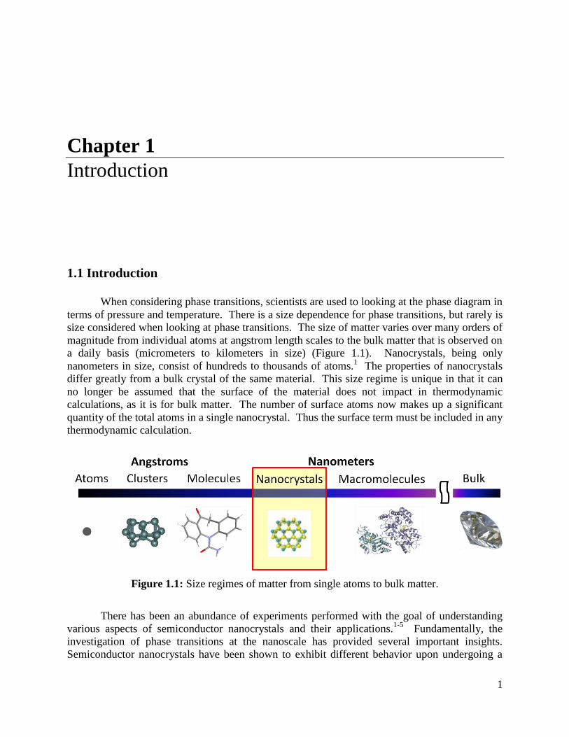
magnitude from individual atoms at angstrom length scales to the bulk matter that is observed on
a daily basis (micrometers to kilometers in size) (Figure 1.1). Nanocrystals, being only
nanometers in size, consist of hundreds to thousands of atoms.1 The properties of nanocrystals
differ greatly from a bulk crystal of the same material. This size regime is unique in that it can
no longer be assumed that the surface of the material does not impact in thermodynamic
calculations, as it is for bulk matter. The number of surface atoms now makes up a significant
quantity of the total atoms in a single nanocrystal. Thus the surface term must be included in any
thermodynamic calculation.
Figure 1.1: Size regimes of matter from single atoms to bulk matter.
There has been an abundance of experiments performed with the goal of understanding
various aspects of semiconductor nanocrystals and their applications.1-5
Fundamentally, the
investigation of phase transitions at the nanoscale has provided several important insights.
Semiconductor nanocrystals have been shown to exhibit different behavior upon undergoing a

2
phase transition when compared to the bulk material. The presence of a thermodynamically
significant surface in the material has a drastic effect on the conditions under which a phase
transition occurs, as evidenced by the fact that the melting point of small nanocrystals can be less
than 50% of that of the bulk material.11
For high pressure structural phase transitions in II-VI
semiconductors it has been found that, unlike bulk single crystals, nanocrystals convert from one
crystal structure to the next without fracturing into multiple domains.7 This is useful when
examining the mechanism and driving forces involved in these phase transitions. In addition to a
change in the thermodynamic phase transition pressure, previous investigations of high pressure
structural phase transitions in nanocrystals have also shown that the transition seems to be under
kinetic control.7 It has been proposed that as the size of the system gets smaller, it reaches a
point where a true solid-solid phase transition ceases to occur and should be considered more
along the lines of a molecular isomerization.6-7
1.2 Nanoparticles
The properties of nanocrystals are highly dependent on size. At small sizes, the number
of surface atoms becomes a high percentage of the total number of atoms in the crystallite. This
means that the surface begins to play a significant role in the properties of the material.6-7,11
In
addition, quantum size effects dominate the electronic and optical properties of the
nanocrystals.1,3
For semiconductors, the combination of these effects yields the ability to tune
the optical and electronic properties of the system by solely changing the size of the
nanocrystal.1,3
In thermodynamic calculations, the surface is typically ignored for simplicity. In bulk
materials, the contribution of the surface is negligible, but it cannot be ignored for nanoparticles.
The surface atoms of a nanoparticle make up a significant number of the total number of atoms
in the system. In thermodynamics, the surface comes into play through the surface area and
surface tension terms. This can be expressed by rewriting the energy equation as:
U=TS-PV+µN-γA (1.1)
where U is the energy, T is the temperature, S is the entropy, P is the pressure, V is the volume,
µ is the chemical potential, N is the number of atoms or molecules, γ is the surface tension, and
A is the surface area of the system. The surface term can manifest itself in the form of size
dependent melting points and phase transitions.6,7,9,11
In semiconductors, the band structure of the material is greatly affected by quantum size
effects.1 As a particle gets smaller, the density of states transitions from the continuous limit for
bulk (3-dimensional) matter to quantized levels for systems that are completely confined (0-
dimensional) matter (Figure 1.2).1,2
This leads to the ability to tune the optical and electrical
properties by using the particle size as the variable instead of the material. More simply put, as
the size of the quantum mechanical box changes, the energy levels available change, as
approximately defined by:
(1.2)
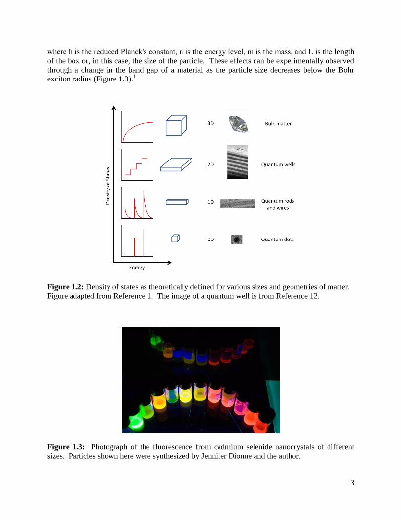
3
where ħ is the reduced Planck's constant, n is the energy level, m is the mass, and L is the length
of the box or, in this case, the size of the particle. These effects can be experimentally observed
through a change in the band gap of a material as the particle size decreases below the Bohr
exciton radius (Figure 1.3).1
Figure 1.2: Density of states as theoretically defined for various sizes and geometries of matter.
Figure adapted from Reference 1. The image of a quantum well is from Reference 12.
Figure 1.3: Photograph of the fluorescence from cadmium selenide nanocrystals of different
sizes. Particles shown here were synthesized by Jennifer Dionne and the author.
4
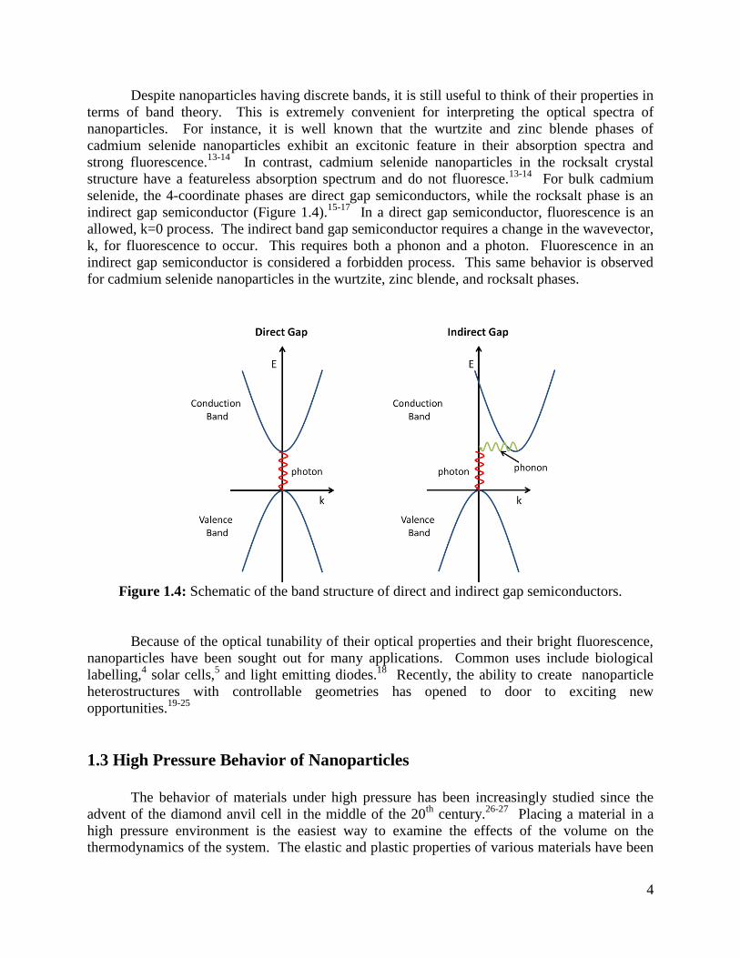
Despite nanoparticles having discrete bands, it is still useful to think of their properties in
terms of band theory. This is extremely convenient for interpreting the optical spectra of
nanoparticles. For instance, it is well known that the wurtzite and zinc blende phases of
cadmium selenide nanoparticles exhibit an excitonic feature in their absorption spectra and
strong fluorescence.13-14
In contrast, cadmium selenide nanoparticles in the rocksalt crystal
structure have a featureless absorption spectrum and do not fluoresce.13-14
For bulk cadmium
selenide, the 4-coordinate phases are direct gap semiconductors, while the rocksalt phase is an
indirect gap semiconductor (Figure 1.4).15-17
In a direct gap semiconductor, fluorescence is an
allowed, k=0 process. The indirect band gap semiconductor requires a change in the wavevector,
k, for fluorescence to occur. This requires both a phonon and a photon. Fluorescence in an
indirect gap semiconductor is considered a forbidden process. This same behavior is observed
for cadmium selenide nanoparticles in the wurtzite, zinc blende, and rocksalt phases.
Figure 1.4: Schematic of the band structure of direct and indirect gap semiconductors.
Because of the optical tunability of their optical properties and their bright fluorescence,
nanoparticles have been sought out for many applications. Common uses include biological
labelling,4 solar cells,
5 and light emitting diodes.
18 Recently, the ability to create nanoparticle
heterostructures with controllable geometries has opened to door to exciting new
opportunities.19-25
1.3 High Pressure Behavior of Nanoparticles
The behavior of materials under high pressure has been increasingly studied since the
advent of the diamond anvil cell in the middle of the 20th
century.26-27
Placing a material in a
high pressure environment is the easiest way to examine the effects of the volume on the
thermodynamics of the system. The elastic and plastic properties of various materials have been

5
investigated in addition to the structural and magnetic phase transitions that occur under high
pressure. Absorption, fluorescence, Raman spectroscopy and X-ray diffraction have been
popular techniques for the characterization of various materials under high pressure.28-29
Recent
advances have also allowed for high pressure experiment to be performed with under high
temperature conditions.30
For bulk semiconductors especially, the phase transitions under high
pressure have been characterized both optically and structurally.15-17,31
As previously mentioned, the surface atoms make up a significant number of the total
atoms in the crystal for nanoparticles. Thermodynamically, this is accounted for by added the
surface term to the free energy equation (Equation 1.1). The inclusion of this term makes the
phase transition conditions of a system size dependent. The consequences of this will be
discussed in Section 1.3.1 for cadmium selenide nanocrystals
The band structure of a semiconductor also changes under pressure, not only due to the
phase transitions, but also due to the change in the volume of the unit cell of the material. This
behavior is fairly well understood and will be discussed briefly in Section 1.3.2.
1.3.1 Thermodynamics and Kinetic Effects
The solid-solid phase transition in cadmium selenide (CdSe) nanocrystals has been
previously investigated in detail.6-8,13-14,32-34
This makes it an excellent case study for the
behavior of nanoparticles under high pressure. During this transition, cadmium selenide goes
from a 4-coordinate tetrahedrally coordinated wurtzite crystal structure to the 6-coordinate
octahedrally coordinated rocksalt structure, with the application of pressure (Figure 1.5). For
CdSe nanocrystals the phase transition occurs at significantly higher pressures than in the bulk.
For instance, a particle with a 1 nm radius undergoes the wurtzite to rocksalt transformation at
4.9 GPa, whereas a particle with a radius of 2.1 nm has a transition at 3.6 GPa.6 In comparison,
the transition for bulk CdSe occurs between approximately 2.0-3.0 GPa.15-17
These phase
transition pressures were determined by averaging the upstroke and the downstroke pressures.
This process assumes a symmetric contribution of the under- and over-pressing to the driving
force, which, although a reasonable estimate, is not accurate for this phase transition.33
It does,
however, provide a reasonable estimate of the thermodynamic values.
Figure 1.5: Crystal structures of wurtzite and rocksalt.
6
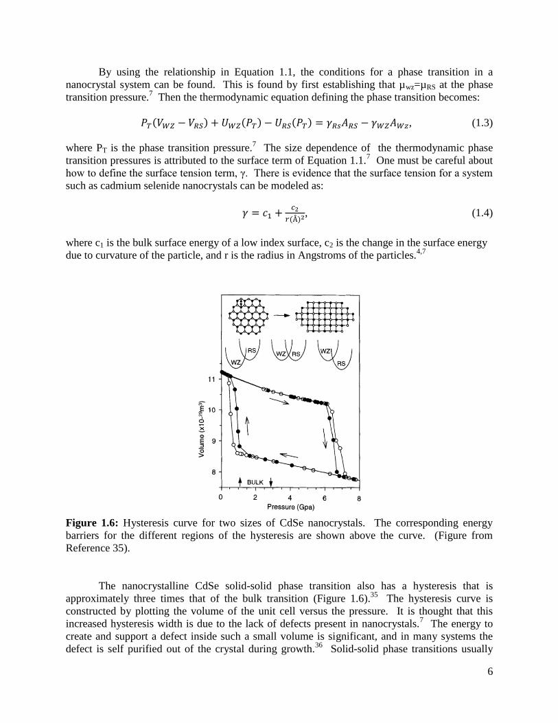
By using the relationship in Equation 1.1, the conditions for a phase transition in a
nanocrystal system can be found. This is found by first establishing that µwz=µRS at the phase
transition pressure.7 Then the thermodynamic equation defining the phase transition becomes:
, (1.3)
where PT is the phase transition pressure.7 The size dependence of the thermodynamic phase
transition pressures is attributed to the surface term of Equation 1.1.7 One must be careful about
how to define the surface tension term, γ. There is evidence that the surface tension for a system
such as cadmium selenide nanocrystals can be modeled as:
, (1.4)
where c1 is the bulk surface energy of a low index surface, c2 is the change in the surface energy
due to curvature of the particle, and r is the radius in Angstroms of the particles.4,7
Figure 1.6: Hysteresis curve for two sizes of CdSe nanocrystals. The corresponding energy
barriers for the different regions of the hysteresis are shown above the curve. (Figure from
Reference 35).
The nanocrystalline CdSe solid-solid phase transition also has a hysteresis that is
approximately three times that of the bulk transition (Figure 1.6).35
The hysteresis curve is
constructed by plotting the volume of the unit cell versus the pressure. It is thought that this
increased hysteresis width is due to the lack of defects present in nanocrystals.7 The energy to
create and support a defect inside such a small volume is significant, and in many systems the
defect is self purified out of the crystal during growth.36
Solid-solid phase transitions usually

7
nucleate at defects in the lattice,37
but without the defects the barrier to nucleation of the rock-
salt phase is greater, leading to the need to overpressure the system to induce a phase transition
in nanocrystals.35
The interfacial energy between the rocksalt nucleus and the surrounding
structure must be surpassed in order for the new phase to propagate.7,35
This energy barrier in
part defines the width of the hysteresis curve.
It should also be noted that upon return to the low pressure phase, CdSe does not form
phase-pure wurtzite crystals. Instead, stacking faults are introduced, making the crystals a
mixture of the wurtzite and zinc blende phases. Thermodynamically speaking, this is not
unexpected as the energy difference between the two structures is small.6
1.3.2 Pressure Effects on the Band Structure
As pressure is exerted on a system, the atoms in that material get closer together,
shrinking the volume. As the distance between the atoms decreases, the overlap between atomic
orbitals increases. Simple molecular orbital theory tells us that when there is a better overlap
between the atomic orbitals, the resultant molecular orbitals split to a greater extent. The band
gap of a material can be shifted a significant amount solely by the application of pressure. In
addition, the bands usually broaden under high pressure. The change in the band gap of a
material under pressure can be equivalent to completely changing the material or alloying.38
Under hydrostatic pressure, this corresponds to a blue shift of the absorption and fluorescence.
Under non-hydrostatic (uniaxial) pressure the shift is not as straight forward. Uniaxial pressure
breaks the symmetry of the crystal. This can result in splitting of the bands relative to the
original symmetry.38
The effect of hydrostatic pressure on many semiconductors has been well
characterized, but the effects non-hydrostatic pressure have proven more difficult to reproducibly
characterize for a variety of factors.38
1.4 Motivation
While the high pressure behavior of simple systems such as CdSe nanocrystals has been
thoroughly studied and is generally well understood, little has been done to investigate more
complicated systems. For instance, the effect of an epitaxial shell grown onto a nanocrystal is
not known. The lattice mismatch at the interface of the two materials could exert a pressure on
the core, changing the pressure at which the phase transition occurs. Disrupting a layered
structure could also change the pressure of a phase transition in these materials. It is unknown
how small changes to the material such as these affect the behavior of the material under high
pressure. From the study of these materials information about the behavior of complex materials
under high pressure and the mechanism of the phase transition can be elucidated. In addition, the
more detailed dynamics of the phase transition on a single nanoparticle level are not known and
can provide additional insight into the mechanism of the phase transition.

8
1.5 Dissertation Outline
The objective of this work was to determine how small changes in structure can tune the
properties of nanomaterials under high pressure. These studies were performed in a hydrostatic
or quasi-hydrostatic environment inside a diamond anvil cell. Effort was taken in trying to
elucidate trends induced by changing the structures of materials in a controlled manner. In
addition, steps towards exposing the mechanism of the wurtzite to rock salt structural phase
transitions were taken through the use of ultrafast pump probe techniques. Chapter 2 of this
dissertation discusses the experimental techniques used to generate high pressure, including
diamond anvil cells and shock waves. In addition, a brief introduction to the colloidal synthesis
of nanoparticles is given. The effect of a zinc sulfide shell of known thicknesses grown on
cadmium selenide nanocrystals is then discussed in Chapter 3. Chapter 4 focuses on the effect of
intercalating copper between the layers of bismuth selenide nanoribbons on the phase transition
of this material. A better understanding of the mechanism of the wurtzite to rocksalt structural
phase transition was gained through the shock compression of cadmium sulfide and is presented
in Chapter 5. Progress towards single particle fluorescence imaging inside a diamond anvil cell
is discussed in Chapter 6. One possible application of the high pressure properties of
nanocrystals for use as a biological force detection is explored in Chapter 7. Future prospects for
investigating the behavior of phase transitions in nanoparticles are presented in Chapter 8.
9
Chapter 2
Experimental Techniques
2.1 Abstract
This chapter introduces the reader to techniques for high pressure generation and the
synthesis of semiconductor nanocrystals. A brief discussion of diamond anvil cells and shock
waves is provided. A general discussion of the reaction procedure used for semiconductor
nanocrystals is supplied. A detailed description of the syntheses performed for the work in this
dissertation can be found in each chapter.
2.2 Introduction
The application of high pressure to a sample is becoming increasingly important in a
multitude of fields, including chemistry, physics and biology. High pressure experimentation
allows for scientists to investigate, in a reversible manner, the effects of changing the volume of
a material. Under high pressure, various phenomena have been observed, including structural,
electronic, and magnetic phase transitions. Depending on the pressures that need to be achieved
for a particular experiment, the pressure conditions to be used, and the geometric requirements of
the monitoring technique, various methods to achieve high pressure exist. Two of these
methods, diamond anvil cells and shock waves, are discussed below.
In addition to the high pressure techniques used throughout this dissertation, a general
discussion of the synthesis of semiconductor nanocrystals is presented in Section 4.
2.3 High Pressure Techniques
Pressure is a fundamental variable in thermodynamics. Changing the pressure that is
exerted on a system changes the energy of that system. As a result, it is an extremely important
variable to consider when looking at the thermodynamics of a material. An important
consideration when performing experiments under high pressure is the nature of the pressure:

10
hydrostatic or non-hydrostatic pressure (Figure 2.1). Hydrostatic, or isotropic, pressure is when
the same pressure is exerted on the sample from all directions. Non-hydrostatic, or anisotropic,
pressure occurs when at least one part of the sample experiences more or less pressure than other
parts of the sample. If the pressure is directed only in one direction, the non-hydrostatic pressure
is called a uniaxial pressure. In the case of non-hydrostatic, the sample will more than likely
change its shape, while a hydrostatic pressure changes the size but not the shape.
Figure 2.1: Hydrostatic pressure exerts an isotropic force on the sample yielding no shape
change. Non-hydrostatic pressure exerts an anisotropic force on the sample and yields a shape
change.
The nature of the pressure can be controlled through the high pressure experimental
method chosen. Diamond anvil cells can be used to exert a hydrostatic or non-hydrostatic
pressure, as determined by the nature of the pressure transmitting medium chosen. Shock waves
typically produce an anisotropic, transient pressure.
2.3.1 Diamond Anvil Cells
Diamond anvil cells (DACs) are a commonly used tool for exerting a static pressure on a
sample up to about 100-150 GPa. A DAC typically consists of two opposing diamonds with flat
culets that press on the gasketed sample between them (Figure 2.2).29
As the backing plates on
which the diamonds are adhered are pushed closer and closer together, a pressure is exerted on
the sample located between the diamonds. Type I or type II diamonds can be used, with type II
diamonds being significantly more expensive, but possessing fewer defects within the crystal
lattice. Diamonds should be chosen for the characterization method to be employed. For
instance, Raman spectroscopy requires diamonds with low fluorescence, a property that can be
found in both type I and type II diamonds.29
Diamonds in the experiments discussed in this
dissertation were about 0.25 carat and brilliant cut.
11
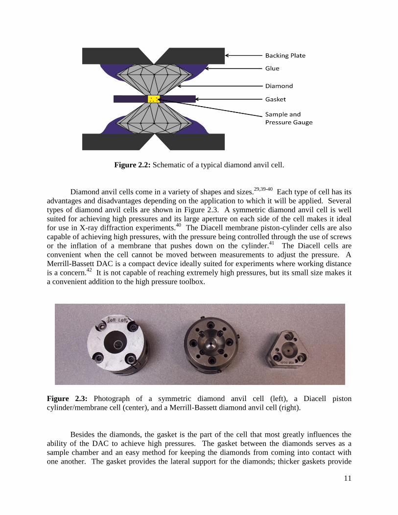
Figure 2.2: Schematic of a typical diamond anvil cell.
Diamond anvil cells come in a variety of shapes and sizes.29,39-40
Each type of cell has its
advantages and disadvantages depending on the application to which it will be applied. Several
types of diamond anvil cells are shown in Figure 2.3. A symmetric diamond anvil cell is well
suited for achieving high pressures and its large aperture on each side of the cell makes it ideal
for use in X-ray diffraction experiments.40
The Diacell membrane piston-cylinder cells are also
capable of achieving high pressures, with the pressure being controlled through the use of screws
or the inflation of a membrane that pushes down on the cylinder.41
The Diacell cells are
convenient when the cell cannot be moved between measurements to adjust the pressure. A
Merrill-Bassett DAC is a compact device ideally suited for experiments where working distance
is a concern.42
It is not capable of reaching extremely high pressures, but its small size makes it
a convenient addition to the high pressure toolbox.
Figure 2.3: Photograph of a symmetric diamond anvil cell (left), a Diacell piston
cylinder/membrane cell (center), and a Merrill-Bassett diamond anvil cell (right).
Besides the diamonds, the gasket is the part of the cell that most greatly influences the
ability of the DAC to achieve high pressures. The gasket between the diamonds serves as a
sample chamber and an easy method for keeping the diamonds from coming into contact with
one another. The gasket provides the lateral support for the diamonds; thicker gaskets provide
12
more support. Unfortunately, this comes with the caveat that a thicker gasket requires more
force, which increases the risk of breaking the diamonds. Thus a balance must be found between
the pressure to be achieved and the amount of support necessary to avoid breakage.29
The gasket
can also determine what geometry the sample can be observed from. For an axial geometry
(probing and collecting through the diamonds), metal gaskets, including stainless steel, spring
steel, and rhenium are typically used.28-29
Typically the harder metals are used for experiments
that are to reach higher pressures. In a radial geometry (probing and collecting between the
diamonds), beryllium and boron epoxy gaskets can be used.43
Because of its toxicity, the use of
beryllium is usually avoided. A gasket also supports the sample material under pressure, which
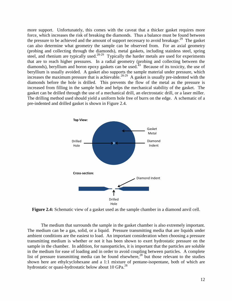
increases the maximum pressure that is achievable.28-29
A gasket is usually pre-indented with the
diamonds before the hole is drilled. This prevents the flow of the metal as the pressure is
increased from filling in the sample hole and helps the mechanical stability of the gasket. The
gasket can be drilled through the use of a mechanical drill, an electrostatic drill, or a laser miller.
The drilling method used should yield a uniform hole free of burrs on the edge. A schematic of a
pre-indented and drilled gasket is shown in Figure 2.4.
Figure 2.4: Schematic view of a gasket used as the sample chamber in a diamond anvil cell.
The medium that surrounds the sample in the gasket chamber is also extremely important.
The medium can be a gas, solid, or a liquid. Pressure transmitting media that are liquids under
ambient conditions are the easiest to load. An important consideration when choosing a pressure
transmitting medium is whether or not it has been shown to exert hydrostatic pressure on the
sample in the chamber. In addition, for nanoparticles, it is important that the particles are soluble
in the medium for ease of loading and in order to avoid coupling between particles. A complete
list of pressure transmitting media can be found elsewhere,28
but those relevant to the studies
shown here are ethylcyclohexane and a 1:1 mixture of pentane-isopentane, both of which are
hydrostatic or quasi-hydrostatic below about 10 GPa.28

13
In addition to the sample and the pressure transmitting medium, the pressure calibrant
must also be included in the sample chamber. Various manometers have been calibrated for use
at the pressures commonly found in DACs, but by far the most commonly used is ruby (α-Al2O3
doped with Cr3+
). The fluorescence of the ruby R1 and R2 is known to shift at a rate of 0.365
nm/GPa.44
This is an easily measured quantity. The splitting and broadening of these peaks with
increasing pressure can also be used to help determine the nature of the pressure inside the DAC
(hydrostatic versus non-hydrostatic). When excited with a blue or a green laser, an electron in
the ground state of the ruby is excited to the Y (4T1) or U (
4T2) band. It then nonradiatively
decays to the E2 level, which is split into 2 levels due to the crystal field. Next, it radiatively
decays to emit the R1 and R2 lines in the ruby fluorescence spectrum (Figure 2.5).44
Other
optical sensors include Sm2+
doped SrB4O7, BaFCl, and SrFCl and Eu3+
doped LaOCl and
Y3Al5O12.28
These have a range of sensitivities and can in some cases also be used to determine
temperature.28
Figure 2.5: Schematic of the electronic levels present in ruby and the R1 and R2 ruby
fluorescence spectrum. (Figure adapted from Reference 44)
In addition to optical manometers, diffraction standards with known equations of states
can be used in a DAC. Commonly used diffraction calibrants are NaCl, CaF2 (fluorite), SiO2
(quartz), CsCl, Al, Au, Pd, Pt, and Ag.28,45
For some of the experiments in this work, the X-ray
diffraction pattern of a small piece of gold included in the sample chamber was used to
determine the pressure in the DAC. The equation of state for gold was used to determine the
pressure from the unit cell volume.46
An example is shown in Figure 2.6.

14
A detailed description of the procedures used to maintain and operate a DAC, including,
alignment and loading procedures, is given in Appendix A.
Figure 2.6: X-ray diffraction patterns of Au with increasing pressure. Synchrotron radiation at a
wavelength of 0.4959 nm was used.
Common methods of monitoring a sample optically in a DAC include absorption and
fluorescence. In order to achieve these, several challenges had to be considered in order to
accommodate the DAC in the optical path. A diagram of the microscope that was built to
address these challenges is given in Figure 2.7. The microscope centers around a Zeiss Axiovert
inverted microscope. A Lexel 95 Ar+ ion laser with a 5 W tube was used as an excitation source.
Typically, the sample was illuminated with the 488 nm line of the laser. The laser power was
controlled using neutral density filters. Because of the size of a DAC, a long working distance
objective must be used. A Zeiss 50× objective with a working distance of 9 mm or a Nikon 20×
objective with a working distance of 23 mm were used to focus within the DAC in an
epiluminescence geometry. To illuminate the sample, a small beam size, typically 5-10 µm, was
necessary to fit within the gasket hole. In general, such a small beam size can be achieved by
using a larger beam size into the back of the objective. The Zeiss Axiovert microscope has a
built in lens in the back of the microscope for use with a halogen lamp. This lens focuses the
laser beam that is directed through the back port to a small point, yielding a large spot size at the
focal point of the objective. Instead of removing the lens, an additional lens was incorporated
into the beam path to adjust the beam such that it was collimated upon reaching the back of the
objective. In this way, a small beam size at the sample could easily be achieved. The emitted
light from the sample in the DAC was then be directed out of the side port of the microscope and
through the slits of an Princeton Instruments Acton SpectroPro 300i spectrometer. The light was
dispersed using a 300 blaze/mm grating for the sample emission and a 1200 blaze/mm grating
for the ruby emission. The signal was then collected using a Princeton Instruments Spec-10
liquid nitrogen cooled CCD. The absorption of the sample within the DAC was collected in a
similar way through the use of a 12V, 100W halogen lamp mounted above the DAC. The signal
collected by the CCD in this case was corrected for the lamp profile in post-collection data
analysis. A setup such as this could easily be modified for Raman spectroscopy.
15
Figure 2.7: A schematic of the absorption and fluorescence microscope used to monitor samples
within the diamond anvil cell.
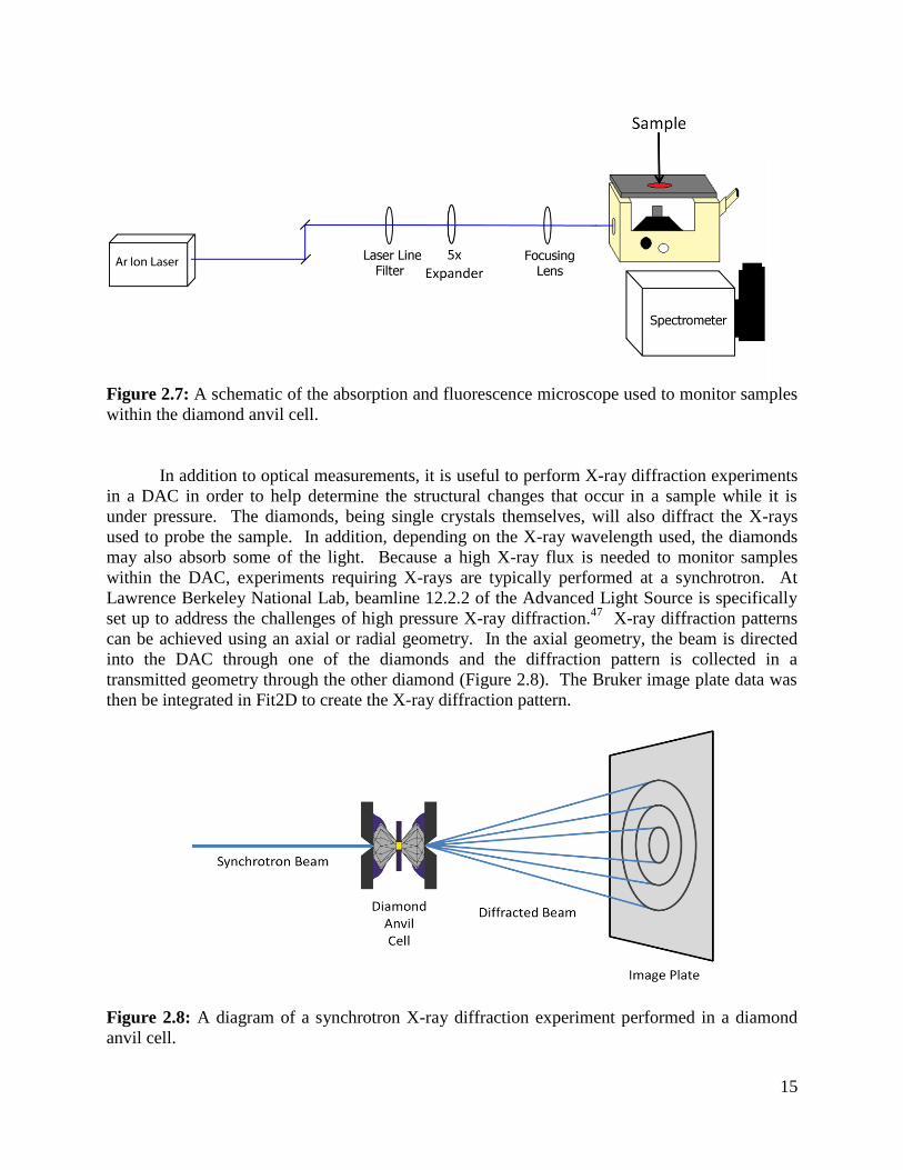
In addition to optical measurements, it is useful to perform X-ray diffraction experiments
in a DAC in order to help determine the structural changes that occur in a sample while it is
under pressure. The diamonds, being single crystals themselves, will also diffract the X-rays
used to probe the sample. In addition, depending on the X-ray wavelength used, the diamonds
may also absorb some of the light. Because a high X-ray flux is needed to monitor samples
within the DAC, experiments requiring X-rays are typically performed at a synchrotron. At
Lawrence Berkeley National Lab, beamline 12.2.2 of the Advanced Light Source is specifically
set up to address the challenges of high pressure X-ray diffraction.47
X-ray diffraction patterns
can be achieved using an axial or radial geometry. In the axial geometry, the beam is directed
into the DAC through one of the diamonds and the diffraction pattern is collected in a
transmitted geometry through the other diamond (Figure 2.8). The Bruker image plate data was
then be integrated in Fit2D to create the X-ray diffraction pattern.
Figure 2.8: A diagram of a synchrotron X-ray diffraction experiment performed in a diamond
anvil cell.

16
2.3.2 Shock Waves
The generation of shock waves has provided a method by which scientists can probe
dynamic, uniaxial compression in materials. Before considering the method by which shock
waves were generated, it is important to first briefly discuss the theory behind shock waves as it
tends to significantly differ from that which is normally discussed for static pressure experiments
performed in a DAC.
Shock waves are typically defined as a plane moving in 1-dimension through a material
that causes a sudden, almost instantaneous change in the thermodynamic parameters, including
pressure, temperature, and volume. Unlike an acoustic wave, which does not cause an overall
change in the average density of a material (it only causes small local changes), a shock wave
can cause a significant change in the density as it traverses the material (Figure 2.9). When a
shock wave transverses through a material, a large number of defects can be created during the
shock and are left behind once the material has return to ambient conditions. A shock wave is
also supersonic, meaning that it travels faster that the speed of sound that is supported by the
material ahead of the shock front.
Figure 2.9: a.) A sound wave traversing a material. The density is the same before and after the
acoustic wave (black line). b.) A shock wave traversing a material. The density behind the
shock front (black line) can be significantly higher than the density in front of the shock.
A shock wave can be described through the use of its jump equations. These equations
define the conservation of mass, momentum, and energy that the shock wave must adhere to due
to thermodynamics. These equations relate the properties of the material behind the shock front
(state 2) to those of the material in front of the shock (state 1):
Mass Conservation: ρ1(U2-u1)=ρ2(U2-u2) (2.1)
Momentum Conservation: P2-P1=ρ1(U2-u1)(u2-u1) (2.2)
Energy Conservation: E2-E1=(P2+P1)(v1-v2)/2, (2.3)

17
where, ρ is the density (g/cm3), U is the shock velocity (cm/µs), u is the particle velocity
(cm/µs), v is the specific volume (cm3/g, 1/ρ), P is the pressure (Mbar), and E is the internal
energy (Mbar-cm3/g).
48-49 The shock velocity, U, and the particle velocity, u, are different
parameters. The shock velocity is defined as the distance that the wave has travelled divided by
the time it took to travel that distance. The particle velocity, on the other hand, is the speed at
which the particles in the material are moving as the shock front traverses the material. The
shock velocity is faster than the particle velocity, as the electromagnetic forces between the
atoms in the material push against the surrounding atoms with a force increasing with decreasing
distance, thus allowing the shock front to travel faster than the atom movement.48
The conservation or jump equations (Equations 2.1- 2.3) can be plotted in the form of a
Hugoniot curve (Figure 2.10).49
Unlike an isoentrope (green line in Figure 2.10), one cannot
simply go from one point to the next continuously on a Hugoniot curve. Each point on a
Hugoniot curve is constructed from drawing a line from the initial state of the material (P0,V0) to
the final state of the material (P1, V1), called the Rayleigh line (blue dashed line in Figure 2.10).
Each point must be determined independently, thus making the Hugoniot a representation of
final shocked states. Because the process is irreversible, the Hugoniot is constructed from a
series of shock experiments starting from the same initial conditions.
Figure 2.10: Schematic showing the P-V Hugoniot, a Rayleigh line, and an isoentrope for a
material.
As shown above, there is a pressure change in the material due to the shock wave. This
stress can be divided into two components: the mean pressure and the shearing stress. The
isotropic mean pressure, , is defined as:
, (2.4)

18
where pi are components of the pressure tensor and the shock wave is travelling in the x-
direction.50
The shearing stress, τ, is defined as:50
. (2.5)
This gives the total pressure measured in a shock wave as:50
. (2.6)
In this case τ is defined as the shear stress on planes with normals 45° to the x-direction. The
value of can be equated to the hydrostatic pressure of static pressure techniques, such as
diamond anvil cells.50
In addition to a pressure increase, the shock wave also causes a change in the temperature
of the sample.49
This temperature rise corresponds to:49
, (2.7)
where
. (2.8)
In Equations 2.7 and 2.8 ΔV=1-V1/V0, Γ is the Grüneisen coefficient, CV is the constant volume
heat capacity, and P is the pressure.
Shock waves can be generated by a number of different methods. Recently, a relatively
simple method using an ultrafast laser to rapidly ablate a thin layer of aluminum thereby
launching a shock wave through the material following the aluminum in the sample stack (Figure
2.11).51
The sample can then be probed from the other side of the stack using a number of
spectroscopic methods. In the case of an X-ray probe, such as a femtosecond pulse from the
free-electron laser at the Linac Coherent Light Source (LCLS) at the SLAC National Accelerator
Laboratory at Stanford University, the probe beam can be aligned in-line with the pump beam
since the material before the sample in the stack is fairly transparent to the X-ray beam (with the
exception of the aluminum, see below). The buffer layer serves the purpose of allowing the
shock front to steepen before it reaches the sample layer.52
The pressure reached by the shock wave travelling through the sample can be determined
by a number of methods. A pressure sensitive dye, such as Rhodamine-640, can be included in
the sample as a calibration standard.53-54
Another option for measuring the shock pressure is to
use the equation of state for the aluminum layer. This can only be used in experiments involving
a X-ray probe.

19
Figure 2.11: An example of the sample stack used to create a shock wave by laser ablation.
2.3.3 High Pressure Diffraction Pattern Analysis
Diffraction patterns for the static and dynamic pressures generated in this dissertation
were analyzed using two different methods. Rietveld refinement is a convenient procedure by
which the structural composition and lattice parameters can be extracted from diffraction data in
a quantitative way.55
Rietveld refinement uses a least squares method to refine a theoretical
pattern to match that of an experimental pattern.56
Multiple theoretical patterns can be input into
the analysis in the case of a mixture of phases. The method is unique in that it is able to handle
overlapping diffraction peaks in a reliable manner. The refined lattice parameters, percent
composition, and particle size (from the Scherrer equation) can be found by using Rietveld
refinement.55,57
A computer program entitled Materials Analysis Using Diffraction (MAUD) has
been developed for performing Rietveld refinement on diffraction patterns.58
MAUD was
extremely useful for the analysis of high pressure diffraction patterns.
For some samples, the background induced from the surrounding medium was too
significant, thus a simple fitting method in Fityk59
or OriginPro 8 was used instead of Rietveld
refinement.
2.3.4 Relevant Parameters Extracted from High Pressure Experiments
In addition to the structural phase of the material, high pressure experiments can provide
insight into the properties of the material under investigation. For instance, when the optical
properties of a semiconductor material under high pressure are investigated, the pressure
dependence of the bandgap can be measured. Such an experiment provides details on whether
the bandgap shifts linearly or sub-linearly with pressure. The optical properties of the materials
can also give insight into the structure of the material. For instance, II-VI semiconductors in the
wurtzite or zinc blende structures are direct gap semiconductors exhibiting excitonic structure in
their absorption and fluorescence.15-17
The same semiconductors in their high pressure rock salt
phase are indirect gap semiconductors, meaning that the absorption spectrum is featureless and
20
the fluorescence is forbidden (it now requires a change in the k-vector in addition to the change
in energy).15-17
From the X-ray diffraction patterns, the volume of the unit cell can be monitored with
changes in pressure. This can provide the bulk modulus of the material. The bulk modulus
defines the resistance of the materials to uniform compression, such as that in a diamond anvil
cell. It is usually represented by the variable B or K and can be calculated through the use of the
equation:
, (2.9)
where P is the pressure and V is the volume.
Since both optical and X-ray diffraction measurements give information about the
structural phase of the material, data from both can be used to construct a hysteresis curve. A
hysteresis curve essentially maps out the phase of the material versus the pressure. The phase
can be represented by the volume of the unit cell, the presence or absence of an absorption or
fluorescence feature, or any other parameter that changes when the phase transition occurs. A
hysteresis curve is constructed by plotting the chosen property against the pressure for both the
upstroke and the downstroke of the pressure sequence. From the resulting loop, information
about the thermodynamics and the kinetics can be obtained.
2.4 Nanoparticle Synthesis
The colloidal synthesis of semiconductor nanoparticles has become a standard procedure
in many laboratories. The colloidal nature of these particles provides for solubility in a variety
of solvents. This allows for the particles to be incorporated into polymer, reacted with other
components in solution, or to be deposited as a solid. This method allows for the facile synthesis
of multi-component nanostructures through the addition of new reagents and for the control of
the shape of the nanostructure. Nanocrystals shaped as dots, rods, tetrapods, and hyper-branched
structures are now regularly synthesized in a reliable manner.2,21-22
The composition of these
structures can be controlled such that different components of the structure can be made of
different materials, allowing for tuning of the optical, catalytic, and mechanical properties of the
resulting nanomaterial.21-22
A general synthetic scheme will be discussed in this chapter. The specifics for the
synthesis of each material used for the work in this dissertation will be discussed in the
respective chapter.
The typical synthetic setup for semiconductor nanoparticles is shown in Figure 2.12.
Nanoparticles were synthesized using standard air free techniques on a Schlenk line. In a
standard reaction, the cation precursor (metal salt or oxide) and the chosen ligand system were
loaded into a 3-neck round-bottom flask equipped with a thermocouple adapter, condenser,
septum, and magnetic stir bar. The system was purged with argon or nitrogen before being

21
heated. The temperature was controlled by a heating mantle and measured by a thermocouple.
The system was rid of oxygen, water, and other low boiling point impurities by placing the it
under vacuum for 1-2 hours. The reaction system was then backfilled with argon and heated to
the temperature desired for injection. The anion solution was rapidly injected into the cation
solution. For nanoparticles with a narrow size dispersion, the injection was performed as quickly
as possible using a large gauge needle. The resulting nanoparticle solution was cooled down to
room temperature. Cleaning of the particles was realized by the addition of an anti-solvent until
the solution was opaque, followed by centrifugation to yield a pellet of nanoparticles. This pellet
was then dissolved in a solvent (typically hexane or toluene), precipitated again with anti-solvent
(acetone or methanol), and centrifuged. The process was repeated until a clear solution of
nanoparticles was achieved.
Figure 2.12: Schematic showing the typical reaction setup for colloidal semiconductor
nanoparticles.
2.4 Conclusion
Methods for the generation of high pressure and the synthesis of semiconductor
nanocrystals have been discussed in general in this chapter. The specifics of each experiment
and synthesis are related in full in their respective chapters.

22
Chapter 3
Structural Phase Transitions and Fluorescence
Splitting in Core/Shell Nanocrystals
3.1 Abstract
High pressure solid-solid phase transitions are strongly dependent on the size of the
nanocrystal. The size dependence of the wurtzite to rocksalt phase transition has been
extensively investigated for core-only CdSe nanocrystals, yet relatively fewer studies have
examined the same phase transition in more complex nanocrystals heterostructures. CdSe/ZnS
core/shell nanocrystals, a prototypical quantum dot system, were synthesized using a successive
ion layer absorption and reaction procedure in order to control the shell thickness. In order to
investigate the high pressure phase transition, the resulting particles were placed into a diamond
anvil and probed using X-ray diffraction, optical absorbance, and fluorescence. The phase
transition hysteresis loops were determined to be dependent on the thickness of the zinc sulfide
shell, indicating changes in both the kinetics and the thermodynamics of the transformation. It
was also found that the mismatch defects are present in the shell for thicknesses greater than one
monolayer, and that fluorescence of the core/shell particles splits into multiple peaks under
pressure due to the presence of the shell. This study highlights the importance of small structural
changes in regard to the high pressure behavior of nanomaterials, and provides insight into how
the forces exerted by the shell influence the core structurally.
3.2 Introduction
Phase transitions are formally defined for systems in which the number of atoms is very
large, and the structural phase diagram is typically considered in terms of pressure and
temperature. Yet there is a size dependence for phase transitions in small systems. The
evolution of the phase diagram as a function of the size in the nanometer size regime is a topic of
much current interest. In nanocrystals, which consist of hundreds to thousands of atoms, the
surface of the material contributes significantly to the thermodynamics of the system. The
surface energy contribution to the energy is different in each phase, and leads to a size
23
dependence of the phase transition. The most well known and dramatic effect of size on a phase
transition occurs for melting, where the melting temperature of small nanocrystals can be less
than 50% of that of the bulk material.11
Melting is a particularly simple case in which to
investigate the nanoscale size dependence, because nucleation is facile. Typically there is very
little hysteresis in this transition for systems comprised of hundreds of atoms or more, and an
abrupt change from solid to liquid and back can typically be observed.
The pressure induced structural transformation in cadmium selenide (CdSe) nanocrystals
has become a model system for studying the size dependence of solid-solid phase transitions.6-
8,13-14,32-35 During this transition, cadmium selenide transforms from a tetrahedrally coordinated
wurtzite or zinc blende crystal structure to the octahedrally coordinated rocksalt structure,
accompanied by a decrease in volume on the order of 20%.33
The nanocrystalline CdSe solid-
solid phase transition also exhibits a hysteresis that is approximately three times that of the bulk
transition.7 This increased hysteresis width is due to the lack of defects present in nanocrystals,
indicating that the transition is under kinetic control, due to a larger barrier for the nucleation of
the new phase.7 It has been proposed that as the size of the system is reduced, it reaches a point
where a true solid-solid phase transition ceases to occur and it should be considered more along
the lines of a molecular isomerization.7
The mid-point of the hysteresis loop of the structural transformation provides a measure
of the thermodynamic transition point. For CdSe nanocrystals, the phase transition occurs at
significantly higher pressures than for the bulk material. For instance, a particle with a 2 nm
diameter undergoes the wurtzite to rock salt transformation at 4.9 GPa; whereas, a particle with a
diameter of 4.2 nm has a transition at 3.6 GPa.6 In comparison, the bulk transition occurs
between 2.0-3.0 GPa.16-17
Furthermore, the upstroke phase transition pressure for 2 nm CdSe
particles is about 9 GPa, while it is only about 7 GPa for 4.2 nm CdSe nanoparticles.6 The fact
the upstroke phase transition is significantly higher than the thermodynamics phase transition
pressure is indicative of the presence of a large energy barrier that must be overcome in order for
the phase transition to occur.
Simulations of nanocrystals under high pressure have previously shown that the
nucleation of the new phase occurs on the surface, followed by its propagation across the entire
nanocrystal.60-61
Typically a single nucleation front can move across a nanocrystal before a
second nucleation event can occur, so that the nanocrystal behaves as a single domain, analogous
to a single domain nanoscale magnet. Given this, it can be easily imagined that altering the
surface in some fashion will change the conditions under which the phase transition occurs.
Advances in the synthesis of colloidal nanocrystals have yielded a facile method for the creation
of more complex nanostructures where the surface can be modified through the addition of an
inorganic shells with differing lattice mismatches and moduli around the outside of the core
particle.19-20
The properties of such a core/shell particle can be compared to those of a quantum
well, as both consist of layered structures whose properties are dependent of the lattice mismatch
between the chosen materials and the layer thickness.
High pressure quantum well experiments point to the ability to tune the phase transition
behavior through layer thickness and composition. Such behavior has been previously observed
in AlAs/GaAs62-64
and CdTe/ZnTe65-67
quantum wells, where not only was there a change in the

24
phase transition conditions, but the kinetics of the phase transition also differed with changes in
layer thickness. For AlAs/GaAs, Weinstein fit the phase transition behavior to an equation based
on the layer thickness and the lattice mismatch.62-64
This relation works for the AlAs/GaAs
system, but is not universally applicable.
Previous high pressure experiments on CdSe/ZnS core/shell experiments have found that
the phase transition in these particles occurs at a higher upstroke pressure relative to pure CdSe
nanoparticles of a similar size.67-68
These experiments did not include an investigation of the
thermodynamic phase transition conditions. In addition, it was found that the addition of the
ZnS shell changes the kinetics of the reverse transition relative to uncapped particles.69
To our
knowledge, no study of the effect of the shell thickness on the phase transition has been
performed. Simulations suggest that there should be a shell thickness dependence for this phase
transition and indicate the possibility of the formation of new stable biphasic structures.70
In the present work, the dependence of the wurtzite to rocksalt phase transition on the
shell thickness was determined. High pressure X-ray diffraction and optical measurements were
carried out in a diamond anvil cell to provide insight into the structure and electronic properties
of the material. Similar to the results from quantum wells, the phase transition pressure was
found to depend on the shell thickness when few defects were present at the interface between
the materials. The variation of the structural and electronic properties with shell thickness was
highly non-monotonic, revealing a complex interplay of structural and electronic phenomena.
Even for thin shells, the shell material was found to exert an anisotropic force on the
nanocrystals. Further, there was strong evidence that a pure ZnS shell breaks up into domains on
the nanocrystal surface at very thin layers between one and two monolayers, confirming the need
for a transition layer of CdS when thicker shells are grown. The work demonstrates that the
phase transition conditions can be modified through a small change in the structure of the
quantum dot.
3.3 Experimental
3.3.1 Synthesis
CdSe nanocrystals were prepared using a literature procedure.
71 Core/shell particles were
synthesized using a successive ion layer absorption and reaction (SILAR) procedure similar to
those presented in References 72 and 73.
Reagents: Cadmium oxide (CdO, 99.99%), stearic acid (98%), and 1-octadecene (ODE, 90%)
were purchased from Alfa Aesar. Octadecylamine (ODA, 97%), selenium powder (99.99%,
-100 mesh), zinc oxide (ZnO, 99.9% powder, < 5 µm), oleic acid (90%), ethylcyclohexane
(99%), methanol, acetone, hexane, and toluene were purchased from Sigma-Aldrich.
Trioctylphosphine oxide (TOPO, 90%) and tributylphosphine (TBP, 99%) were purchased from
STREM. Sulfur powder (sublimed) was purchased from Fisher. NOTE: TBP is slightly
pyrophoric and should be handled accordingly.

25
Cadmium Selenide Cores: In a small vial, 158 mg of Se powder and 0.472 g TBP were
combined and stirred at room temperature under argon until the mixture went clear and colorless.
In a 25 mL three-neck roundbottom flask equipped with a condenser, thermocouple adapter,
magnetic stir bar, and septum, 25 mg of CdO, 227 mg of stearic acid, and 2.53 mL of ODE were
combined. Under flowing argon, the mixture was heated to 200 °C. When the solution turned
clear and colorless, the reaction mixture was cooled down to room temperature. ODA (1.5 g)
and 0.5 g of TOPO were added to the reaction and the reaction was heated to 280 °C under
argon. The TBP:Se precursor was then quickly injected into the mixture quickly using a 16-
gauge needle. The reaction was grown for 30 seconds to yield nanoparticles about 3.5 nm in
diameter. Size control could be achieved by varying the growth time after the injection. The
reaction mixture was cooled rapidly to room temperature, where about 7 mL of hexane was
added and the entire solution was transferred to a glovebox. The resulting nanoparticles were
cleaned first by layering the reaction mixture with methanol and removing the resulting colorless
or white layer several times. Subsequent cleaning was performed through the addition of
acetone until the colored solution was cloudy followed by centrifugation. The resulting pellet
was dissolved in hexane or toluene and the precipitation procedure was repeated until a clear,
colored solution in hexane was achieved. The solution concentration of the CdSe nanocrystals
was determined using the equations from Reference 74.
Zn(oleate)2 Precursor: In a 50 mL three neck roundbottom flask equipped with a condenser,
thermocouple adapter, magnetic stir bar, and septum, 203 mg of ZnO, 6.91 mL of oleic acid, and
18 mL of ODE were combined. The mixture was heated to 250 °C under flowing argon. When
all of the ZnO had dissolved, the precursor solution was cooled to 70 °C and transferred to a
purged Schlenk flask, before cooling to room temperature. Injections for the SILAR reaction
(see below) were performed with the zinc precursor solution at 80 °C to prevent the solidification
of the zinc oleate.
Sulfur precursor: In a 50 mL three neck roundbottom flask equipped with a condenser,
thermocouple adapter, magnetic stir bar, and septum, 64 mg of sulfur and 20 mL of ODE were
combined. The mixture was heated to 170 °C under flowing argon until the sulfur was
completely dissolved. The solution was then cooled to room temperature and transferred to a
purged vial for future use. Injections for the SILAR reaction (see below) were performed with
the sulfur precursor at room temperature.
Shell Deposition: The amount of each precursor needed for each layer was calculated according
to the method described in the literature.23
In a 50 mL three neck roundbottom flask equipped
with a condenser, thermocouple adapter, magnetic stir bar, and septum, 3 mL of ODE and 1 g of
ODA were combined. The mixture was heated to 100 °C under vacuum for 1 hour. After 1
hour, the reaction flask was backfilled with argon and 1.83×10⁻⁷
moles of CdSe nanocrystals in
hexane were injected. The solution was then heated to 120 °C under vacuum for 45 minutes to
remove the hexane. The reaction flask was then backfilled with argon and heated to 190 °C.
Enough of the zinc precursor for a single monolayer was then added over several minutes in a
dropwise manner. The reaction was then allowed to stir for 20 minutes before the same amount
of sulfur was added dropwise and the particles were again allowed to react again for 20 minutes.
Subsequent injections could be done at 210 °C. Temperatures higher than these yielded some
alloying, as indicated by a blue shift in the absorption. The procedure was repeated until the
26
desired shell thickness was reached. Once the desired shell thickness was achieved, the reaction
mixture was cooled down to room temperature and the solution was transferred to a glovebox.
The cleaning procedure was similar to that of the CdSe cores discussed above. Once the
nanoparticles were isolated they were dissolved in hexane or ethylcyclohexane. This synthesis
yields a small amount of self-nucleated ZnS particles that are difficult to separate from the
core/shell particles.
Characterization: Particles were characterized using transmission electron microscopy in
addition to absorption and fluorescence. Absorption was collected on a Agilent 8453 UV-vis,
while fluorescence was performed on a Horiba Fluorolog. A FEI Tecnai G2 S-Twin transmission
electron microscope operating at 200 kV using a LaB6 filament was used to image the
nanocrystals.
3.3.2 High Pressure Experiments
3.3.2.1 Diamond Anvil Cell
High pressure experiments were performed using a symmetric diamond anvil cell (DAC)
from Princeton. Pressure was generated using diamonds with a 300 µm culet size. Spring steel
gaskets were pre-indented to ~80 µm in thickness and drilled using an Oxford laser miller or an
electrostatic drilling machine. Several grains of annealed ruby44
or a small piece of gold foil46
was placed in the gasket hole using a small needle prior to the sample for the purpose of
measuring the pressure inside the DAC. The sample dissolved in ethylcylcohexane was then
added and the DAC was sealed. Samples used for X-ray diffraction were necessarily of a higher
concentration than those used for the optical experiments.
3.3.2.2 High Pressure X-Ray Diffraction Experiments
High pressure X-ray diffraction measurements were performed on beamline 12.2.2 at the
Advanced Light Source at Lawrence Berkeley National Lab. The data was collected using an
energy of 25 keV (0.4959 Å). Typical acquisition times for the nanoparticle sample ranged from
10-20 minutes per pressure, while those of the gold pressure calibrant were 1-2 minutes. The
beam size for samples ranged from 20-40 µm by 20-40 µm. For the gold calibrant, the beam size
was 10 µm by 10 µm. Data was collected in a transmission geometry using a MAR345 image
plate. The detector distance and tilt were calibrated with a LaB6 (NIST) standard. The resulting
two-dimensional XRD images were integrated to one-dimensional powder patterns using
FIT2D.75
3.3.2.3 High Pressure Absorption and Fluorescence Experiments
High pressure optical experiments were performed using a Zeiss Axiovert inverted
microscope that was configured to perform absorbance and fluorescence spectroscopy. The
microscope was equipped with a Lexel 95 Ar+ laser, which was set to emit the 488 nm line for
the sample and ruby excitation. The beamsize of the laser was about 5-10 µm. Absorption
spectra were collected by using a 12V, 100W halogen lamp mounted above the DAC. A Nikon
20× objective with a working distance of 23 mm was used to focus inside the DAC. The light

27
transmitted (absorption) or emitted (fluorescence) by the sample was directed through a Acton
SpectroPro 2300i spectrometer and collected on a Princeton Instruments Spec-10 liquid nitrogen
cooled CCD.
3.3.3 Data Analysis
The XRD peaks were fit to Pearson VII functions in Fityk.
76 The optical data was fit to
Gaussians using OriginPro 8.0.
3.4 Results
The transmission electron micrographs of the synthesized particles are shown in Figure
3.1. As expected, the particle size distribution widens with increased shell thickness and the
particle shape becomes less spherical due to defects introduced by the lattice mismatch.
Analysis of the TEM images indicates that each successive injection caused the particles to grow
by approximately a monolayer (ML) of ZnS. The shell thicknesses used in this study were 0.4
nm (~1 ML), 0.6 nm (~2 ML), and 1.1 nm (~3 ML). For all samples, the CdSe core size was
kept consistent, while the shell thickness was changed.
Figure 3.1: Examples of TEM micrographs for CdSe and CdSe/ZnS core/shell nanoparticles.
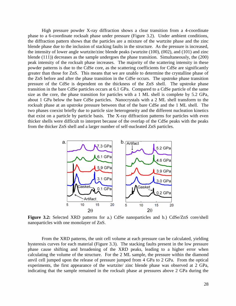
28
High pressure powder X-ray diffraction shows a clear transition from a 4-coordinate
phase to a 6-coordinate rocksalt phase under pressure (Figure 3.2). Under ambient conditions,
the diffraction pattern shows that the particles are a mixture of the wurtzite phase and the zinc
blende phase due to the inclusion of stacking faults in the structure. As the pressure is increased,
the intensity of lower angle wurtzite/zinc blende peaks (wurtzite (100), (002), and (101) and zinc
blende (111)) decreases as the sample undergoes the phase transition. Simultaneously, the (200)
peak intensity of the rocksalt phase increases. The majority of the scattering intensity in these
powder patterns is due to the CdSe core, as the scattering coefficients for CdSe are significantly
greater than those for ZnS. This means that we are unable to determine the crystalline phase of
the ZnS before and after the phase transition in the CdSe occurs. The upstroke phase transition
pressure of the CdSe is dependent on the thickness of the ZnS shell. The upstroke phase
transition in the bare CdSe particles occurs at 6.1 GPa. Compared to a CdSe particle of the same
size as the core, the phase transition for particles with a 1 ML shell is complete by 5.2 GPa,
about 1 GPa below the bare CdSe particles. Nanocrystals with a 2 ML shell transform to the
rocksalt phase at an upstroke pressure between that of the bare CdSe and the 1 ML shell. The
two phases coexist briefly due to particle size heterogeneity and the different nucleation kinetics
that exist on a particle by particle basis. The X-ray diffraction patterns for particles with even
thicker shells were difficult to interpret because of the overlap of the CdSe peaks with the peaks
from the thicker ZnS shell and a larger number of self-nucleated ZnS particles.
Figure 3.2: Selected XRD patterns for a.) CdSe nanoparticles and b.) CdSe/ZnS core/shell
nanoparticles with one monolayer of ZnS.
From the XRD patterns, the unit cell volume at each pressure can be calculated, yielding
hysteresis curves for each material (Figure 3.3). The stacking faults present in the low pressure
phase cause shifting and broadening of the XRD peaks, leading to a higher error when
calculating the volume of the structure. For the 2 ML sample, the pressure within the diamond
anvil cell jumped upon the release of pressure jumped from 4 GPa to 2 GPa. From the optical
experiments, the first appearance of the wurtzite/ zinc blende phase was observed at 2 GPa,
indicating that the sample remained in the rocksalt phase at pressures above 2 GPa during the

29
downstroke. From this it can be assumed that the shape of the hysteresis curve for the 2 ML
sample is similar to those of the bare CdSe and the 1 ML samples.
Figure 3.3: Pressure-volume hysteresis curves for the wurtzite/zinc blende phase to the rocksalt
phase under high pressure for the CdSe control and the core/shell samples with one and two
monolayers of ZnS.
In addition to the structural information obtained from the XRD data, optical data was
also collected in the form of absorption and fluorescence spectra. The absorption patterns of all
the samples show the expected blue shift with increasing pressure, with the eventual
disappearance of the exciton due to the transition to the rocksalt phase, which has an indirect
band gap. The fluorescence spectra of the bare CdSe particles under pressure also exhibit an
overall blue shift with pressure in addition to some peak broadening. In contrast, the
fluorescence spectra of the core/shell particles shows significant peak splitting with increased
pressure (Figure 3.4). The fluorescence eventually disappears, indicating the transition to the
high pressure indirect structure.
3.5 Discussion
Unlike previous studies investigating the phase transitions in CdSe/ZnS core/shell
nanocrystals, this study shows a direct comparison to CdSe with no shell under identical
conditions. This allows for differences in the pressure environment due to the hydrostaticity or
non-hydrostaticity of the pressure transmitting medium to be removed from the analysis.
Ethylcylcohexane is a quasi-hydrostatic pressure transmitting medium commonly used in
diamond anvil cell experiments.10
Because it is quasi-hydrostatic, some shear may be present in
the diamond anvil cell.

30
Figure 3.4: The fluorescence spectra of CdSe nanoparticles (a) and CdSe/ZnS nanoparticles with
one monolayer of ZnS (c) with increasing pressure are shown. The corresponding peak positions
for the CdSe nanoparticles (b) and the CdSe/ZnS core/shell nanoparticles (d) describe the
observed peak splitting with increasing pressure.
From the hysteresis curve, it is obvious that the initial unit cell volume for nanoparticles
with a ZnS shell is smaller than the bare CdSe nanoparticles. The ZnS shell has smaller lattice
parameters than that of the CdSe core, causing it to compress the CdSe core. Previous
simulations have indicated that this compression should be less than 1 GPa for a single
monolayer of ZnS and about 1.5 GPa for a shell with a thickness on the order of two monolayers
of ZnS.70
Using the bulk modulus of CdSe nanoparticles in the wurtzite phase,7 we calculated
that the pressure felt by the core with one monolayer of ZnS was about 2 GPa. When taking into
account the error introduced into the measurement due to the presence of stacking faults and the
diffraction from a small number of pure ZnS nanoparticles, this is within error of the calculated
pressure.
The upstroke phase transition pressure is clearly dependent on the shell thickness. The
decrease in the phase transition pressure and the width of the hysteresis loop for the core/shell
particles with one monolayer of ZnS can be attributed to a change in the nanoparticle surface.
Previous simulations have indicated that during this phase transition the nucleation of the new
phase occurs on the surface, meaning that the phase transition conditions could be altered if the
surface was significantly changed.60-61
The first monolayer of ZnS could restructure the surface
such that nucleation of the new phase is easier. Once mismatch defects are induced due to a
31
shell thickness greater than the critical thickness, the structure may relax back to a structure
resembling that of the bare core, causing the phase transition pressure to rise again. The upstroke
phase transition in the particles with a shell thickness of two monolayers is greater than the
observed conditions for a pure CdSe particle of a size similar to that of the core plus the shell,
but about the same as a pure CdSe nanoparticle of the same size of just the core. In addition to
the surface restructuring due to the addition of the ZnS shell, the shell also introduces a biaxial
strain at the surface due to the lattice mismatch. This strain changes the pressure environment
that the core experiences from quasihydrostatic to anisotropic, thus introducing a stronger shear
into the system. The shear can also lower the observed phase transition pressure of the core/shell
particles relative to bare CdSe particles.
The restructuring of the surface and the introduction of mismatch defects into the lattice
of the core/shell nanocrystal provide sites for the nucleation of the new phase. This lowers the
activation energy necessary to transition from one phase to the next, causing a reduction in the
upstroke phase transition pressure and an increase in the downstroke phase transition pressure.
This results in the shrinking of the width of the hysteresis curve when a ZnS shell is included in
the nanostructure.
The thermodynamic phase transition pressure, as measured from the middle of the
hysteresis curve, also shifts with the shell thickness. The initial decrease in the thermodynamic
phase transition pressure can be attributed to the expitaxial nature of the first monolayer. The
lattice mismatch between the CdSe core and the ZnS shell should result in a pressure being
exerted on the core by the shell. This has been previously modeled by Grunwald et al.70
The
phase transition pressure in this case would then be the external pressure exerted in the diamond
anvil cell plus the pressure exerted by the ZnS shell. For greater shell thicknesses, defects are
introduced at the interface due to the shell thickness being greater than the critical thickness for
the epitaxial growth of ZnS on CdSe. These mismatch defects relax the structure, reducing the
pressure exerted on the core by shell. As a result, the phase transition to occur at a pressure
closer to that of the bare core for shells thicker than 1 ML.
The optical properties of these core/shell semiconductor nanocrystals also differ from
those of bare CdSe nanocrystals. The fluorescence of the bare CdSe remains approximately a
single Gaussian peak throughout the pressure upstroke, with a small deviation before the phase
transition. In contrast, the fluorescence of particles with a ZnS shell, regardless of shell
thickness, split into multiple Gaussians peaks. Because the same splitting is not seen in the
particles without a shell, it cannot be attributed solely to the pressure environment within the
diamond anvil cell. Instead, the splitting of the fluorescence peak must be due, in part, to the
presence of the shell. The lattice mismatch between the core and the shell creates a biaxial strain
that changes the pressure environment that is felt by the core. This biaxial strain, in combination
with the quasi-hydrostatic pressure environment, cause at least some of the nanoparticles to be
compressed in an anisotropic manner.
Under uniaxial pressure, the symmetry of the crystal structure of the nanoparticles is
broken. It was previously found for bulk II-VI semiconductors that the behavior of the band
structure dependence depends not only on the direction and magnitude of the applied
deformation, but also the spin exchange in the excitons.77-78
Since the splitting of the valence
32
band is small, within kBT, it is possible to observe radiative emission to all of the levels. This
explains the observed splitting in the fluorescence of the core/shell particles. The fluorescence
measurement is on an ensemble level, meaning there is a random orientation of particles relative
to the polarization of the incoming laser light and presumably, a large distribution in the
direction of applied pressure relative to the crystal axes. This makes the consideration of
polarization and the direction of the applied uniaxial pressure unnecessary for our ensemble
measurements.
It is of interest to consider these results in the broader context of studies of core-shell
quantum dots. The present experiment shows evidence that the strong lattice mismatch between
CdSe and ZnS results in a modification of the electronic energy levels of the core for thicknesses
as small as one monolayer, and the introduction of defects in the shell for surprisingly thin shells
that are just above a monolayer in thickness. The widespread practice of growing a graded shell
of CdS to ZnS to relieve the strain makes sense in this context, and appears to be highly desirable
if the structural integrity of the core-shell interface is important. The chemical and
photochemical stability of a core-shell quantum dot can be comprised if the core/shell interface is
defective, as appears to occur for ultra-thin layers of ZnS grown directly on CdSe.
3.6 Conclusions
This study shows that the phase transition in core/shell CdSe/ZnS nanoparticles is
strongly dependent on the shell thickness, and that the dependence is not monotonic even for
very thin shells. In addition, the study of the optical properties of these nanoparticles under high
pressure showed a splitting of the fluorescence peak that can only be explained by the shell
exerting an anisotropic force on the core. Future work may focus on how the degree of lattice
mismatch can be used to tune the high pressure behavior of these nanoparticles in a wider range
of core and shell compositions.

33
Chapter 4
Suppression of High Pressure Phase Transitions
in Two-Dimensional Layered Bi2Se3
Nanocrystals
4.1 Abstract
Previous high-pressure studies in the layered chalcogenide, Bi2Se3, have revealed rich
and unusual physics including a structural phase transition from a rhombohedral to monoclinic
structure and an electronic topological transition. As a layered material, Bi2Se3 possesses a van
der Waals gap which can serve as a host for intercalant guests, further altering the electronic and
structural behavior of the material. Recently, a method to intercalate high densities, up to 60
atomic percent, of zero-valent copper into Bi2Se3 nanoribbons was developed. Using X-ray
diffraction, the high-pressure structural behavior of Bi2Se3 nanoribbons and copper-intercalated
Bi2Se3 nanoribbons was investigated using a diamond anvil cell and a synchrotron source. The
nanoribbons of Bi2Se3 undergo a structural phase transition from a rhombohedral structure (R m)
to a monoclinic (C2/m) phase at a higher phase transition pressure that that of the bulk material.
The intercalation of copper into the gaps between the layers in the nanoribbons further raises the
transition pressure and alters the electron topological transition.
4.2 Introduction
4.2.1 Topological Insulators
Topological insulators are a newer class of materials with very interesting properties.
Like normal insulators, topological insulators possess a band gap between the highest occupied
electronic band and the lowest unoccupied electronic band. But unlike the ordinary insulators,
the surface states (or edge states in the case of 2-D materials) of topological insulators do not
exhibit this gap. Instead they provide a gapless series of states connecting the conduction and

34
valence bands. Such materials could find applications in device physics in addition to filling a
gap in our understanding of band theory.
4.2.2 Bismuth Selenide and Copper Bismuth Selenide
Bi2Se3 has attracted much interest as part of a new class of three-dimensional topological
insulators. 79-81
This has spurred many investigations into controlling the synthesis, properties,
and chemical behavior of this material. Bi2Se3 is a layered chalcogenide. Quintuple layers of
alternating Se and Bi (Se-Bi-Se-Bi-Se) sheets form the two-dimensional layers found in the
rhombohedral phase. These quintuple layers are separated from one another by a van der Waals
gap. Because of their layered structure, two-dimensional layered materials, such as Bi2Se3, are
easy to chemically modify through the accommodation of atoms in the van der Waals gap
between the layers.
Recently, the ability to intercalate high densities of zero-valent metals, including copper,
gold, silver, and cobalt, into layered Bi2Se3 nanoribbons has been achieved.82-83
By tuning the
type and concentration of the intercalated species, the electronic and structural properties of the
material can be altered, giving rise to superconductivity or unique electronic states.83-86
High
pressure is a key tool in further achieving novel electronic and structural states.
Previous investigation of bulk Bi2Se3 have shown that there is a pressure induced
structural phase transition from the rhombohedral (R m, space group 166) layered structure to a
monoclinic (C2/m, space group 12) structure.87
In bulk investigations, this structural phase
transition commences around 8 GPa.88
As the dimensionality of this material is reduced, fewer
and fewer layers are incorporated into the structure, allowing surface effects to begin to dominate
the structural phase behavior. Such size dependent behavior of phase transition has been
previously observed in other materials.7,11,89
In addition to the structural phase transition, literature demonstrates the presence of an
electronic topological transition (ETT) in Bi2Se3 under pressure.87,90
An ETT is a second-order
isostructural transition where the shape of the Fermi surface undergoes a transition. In these
layered chalcogenide materials, this type of transition likely corresponds to a pressure where the
van der Waals gap has been compressed almost entirely out of the crystal, leading to some type
of overlap resulting in a change in the Fermi surface. Previous calculations have shown that
without taking into account the surface states, Bi2Se3 is an indirect semiconductor at ambient
pressure, with a conduction band minimum at the Γ point and the valence band maximum
halfway between the Γ and U points.91
At pressures above 5 GPa, the band gap becomes direct,
with the gap halfway along the Γ-U direction.91
While this change in the band structure has not
been directly linked to the ETT, it could play a role in the shape change of the Fermi surface.
Because the bulk band structure of Bi2Se3 has a gap at the Fermi energy, there is no Fermi
surface until the surface states are included. Some of the surface states occupy the band gap,
allowing for the calculation of a Fermi surface to be possible.79-81
Such a transition does not
exhibit a discontinuity in the unit cell volume upon undergoing the transition, but does exhibit a
change in the compressibility. Previous high pressure experiments on Bi2Se3 and Bi2Te3 have
shown that the rhombohedral phase shows a change in the compressibility as the pressure is

35
increased.87,92-95
This has been found to be a reliable indication of an ETT in these layered
chalcogenides.90
In this work, synchrotron X-ray diffraction experiments were conducted to investigate the
high-pressure behavior of Bi2Se3 nanoribbons, with a focus on the pressure-induced phase
transitions. The phase transition pressure of pure Bi2Se3 nanoribbons is compared with that of
copper-intercalated Bi2Se3 nanoribbons (45 atomic percent of copper). It was found that the
presence of copper in the lattice increases the structural phase transition pressure and affects the
electronic topological transition.
4.3 Experimental
4.3.1 Synthesis
Bi2Se3 nanoribbons (Figure 1; top) were prepared using a vapor-liquid-solid (VLS)
growth method described elsewhere.96
A source powder of Bi2Se3 was placed in a 1' tube
furnace at 550°C. The carrier gas, argon, transports the sublimed powders to a colloidal gold
coated quartz growth substrate downstream. A high density of zero-valent copper was
intercalated into Bi2Se3 nanoribbons (Figure 1; bottom) using the method from References 82
and 83. Briefly, Bi2Se3 nanoribbons on the quartz growth substrate were placed into a solution
of 0.01 g of tetrakisacetonitrile copper(I) hexaflourophosphate in acetone just below reflux
(51°C) for four hours. The final concentration of intercalated copper in these samples was 45
atomic percent as determined by energy-dispersive X-ray spectroscopy (EDX) and X-ray
photoelectron spectroscopy (XPS).82-83
4.3.2 Data Collection
High pressure X-ray diffraction measurements were performed on Beamline 12.2.2 of the
Advanced Light Source at Lawrence Berkeley National Lab using an energy of 25 keV (0.4959
Å). Typical acquisition times were 1-5 minutes per pressure data point. A spot size of 10 µm ×
10 µm was used. Pressures were generated in a symmetric diamond anvil cell (DAC) with 300
µm culets. Spring steel gaskets were pre-indented to ~80 µm thickness and drilled using an
Oxford laser miller. A 4:1 methanol:ethanol pressure transmitting medium was used, which is
hydrostatic to about 10 GPa.28
The sample was loaded by placing several nanoribbons in the
gasket hole using a needle before the pressure-transmitting medium was added and the DAC
sealed. Several grains of annealed ruby were also placed in the gasket hole in order to measure
the pressure inside the DAC.44
Ruby fluorescence was excited with a 488 nm Ar+ laser. The
degree of hydrostaticity was determined by the line width of the ruby fluorescence.44
4.3.3 Data Analysis
The detector distance and tilt relative to the sample were calibrated with a LaB6 (NIST)
standard. Two-dimensional XRD images were integrated to one-dimensional powder patterns
using FIT2D.75
Peaks were fit to Gaussians using Mathematica. The pressure-volume data was

36
fit to a Birch-Murnaghan equation of state using EosFit v5.2.97
Atomic structures were
visualized using Jmol.98
4.4 Results and Discussion
Bi2Se3 nanoribbons were synthesized via the vapor-liquid-solid method (see
experimental). Zerovalent copper was intercalated into the van der Waals gap of the structure for
one of the nanoribbon samples. No evidence of copper precipitates or particles was observed in
the TEM or the XRD. Both structures were highly crystalline, as evidenced by the TEM images
and electron diffraction shown in Figure 4.1.
Figure 4.1: TEM images of nanoribbons (inset) of Bi2Se3 and copper intercalated Bi2Se3 used in
this study. Electron diffraction (inset) and high resolution TEM images show these particles are
highly crystalline.

37
High pressure X-ray diffraction of Bi2Se3 nanoribbons and copper-intercalated Bi2Se3
nanoribbons revealed markedly different phase transitions conditions (Figure 4.2; left and
center). At pressures less than 10.3 GPa, the pure Bi2Se3 nanoribbons were in the rhombohedral
phase (Figure 4.2). At 10.3 GPa, the nanoribbons were a mixture of the rhombohedral and
monoclinic structural phases. The phase transition was complete after 12 GPa. This is
significantly higher than the phase transition pressure in bulk Bi2Se3 which exhibited a phase
transition that commenced at 8 GPa.88
It is well known that crystallite size plays an important
part in the phase transition pressure due to the role of surface effects.7,89
Fewer layers are
incorporated into the crystal as the crystal gets thinner. This allows the surface to begin to
dominate the thermodynamics, changing the phase transition conditions.
Figure 4.2: XRD patterns of Bi2Se3 nanoribbons (left) and nanoribbons intercalated with copper
(center). Bi2Se3 undergoes a phase transition from a rhombohedral (R m) structure to a
monoclinic (C2/m) (right). Purple atoms represent bismuth, while yellow atoms are selenium.
The structural phase transition from the rhombohedral phase to the monoclinic phase is
driven by a collapse of the van der Waals gap between the layers. As the layers are forced closer
together, their attraction becomes so strong that the material undergoes a phase transition. By
inserting copper into the host lattice, it becomes more difficult to compress the gap due to a
disruption of the van der Waals force between the quintuple layers, allowing for a higher phase
transition pressure. The phase transition in the copper intercalated nanoribbons is not complete
even at 12 GPa (Figure 4.2). In both samples, upon release of pressure the high pressure
monoclinic phase transformed back to the ambient rhombohedral structure (Figure 4.2).

38
By fitting the XRD data, the lattice parameters of the low pressure rhombohedral phase
were obtained. The change in the a-axis with pressure appears to be approximately linear, but
that of the c-axis deviates from a line. In addition, the c-axis lattice parameter changes
significantly more than that of the a-axis. The quintuple layers are stacked along the c-axis,
allowing for significant compression of the gap between layers before the phase transition. As
the gap collapses, the layers get closer together, making compression of the material along the c-
axis more difficult, accounting for the deviation from linearity observed in Figure 4.3. In
contrast, the layers are parallel to the a-axis. This does not allow the crystal to be compressed to
the same extent along the a-axis as the c-axis due to the interatomic repulsion between nearest
neighbor atoms within the layers.
Figure 4.3: Lattice parameters for the a- and c-axes, as a function of pressure for Bi2Se3 (blue
circles) and Cu-Bi2Se3 (red circles) are shown. The inset plot shows the c/a ratio.
A dramatic change in the slope of the c/a ratio versus pressure was also observed (Figure
4.3; inset). Such a change has been previously observed in bulk Bi2Se3 and has been found to be
indicative of an ETT.87,90
For the copper intercalated nanoribbon sample, the change in slope of

39
the c/a ratio is not observed until after 6 GPa, pronouncedly higher than the sample without
copper, where the change in slope occurs at about 3 GPa. This is due to the copper atoms
disrupting the van der Waals force between the layers. Doping the structure with copper also
changes the Fermi level in the Bi2Se3, providing the potential for a change in the initial shape of
the Fermi surface, which would then change in a different manner at high pressure. This changes
the conditions under which the ETT occurs.
Figure 4.4 shows the change in the volume of the rhombohedral and monoclinic phases.
The pressure-volume data was fit to a third-order Birch-Murnaghan equation of state.99
For the
Bi2Se3 nanoribbons, the following parameters were determined: V0=142.9(4) Å3, B0=35(3) GPa,
and =7. For the Cu-Bi2Se3 nanoribbons, the error of the fit was higher, yielding V0=143(3)
Å3, B0=27(16) GPa, and
=14(10). For both these samples, the calculated bulk modulus agreed
within error with that reported in Reference 90. Upon undergoing the ETT, there is no
discontinuous change in the volume (Figure 4.4). This is expected, as the ETT is a second-order
transition. The structural phase transition from the rhombohedral phase to the monoclinic phase
exhibits a discontinuous change in volume, indicating a first order transition. These results agree
with previous investigations of the phase transition in bulk Bi2Se3.87,90
Figure 4.4: The volume of the unit cell with pressure.
4.5 Conclusions
This work presents the ability to tune the phase transition pressure in two dimensional
layered nanostructures, such as Bi2Se3, through the intercalation of a metal into the van der
Waals gap. In addition to an overall higher phase transition due to the crystallite size, the
intercalated metal disrupts the forces between the layers leading to a higher phase transition
pressure. Future studies should look at the dependence of the phase transition pressure on the
percent intercalation of the metal and if there is a dependence of the metal used.

40
Chapter 5
Ultrafast Observations of Structural Phase
Transition Pathways in Nanocrystals Using a
X-Ray Probe
5.1 Abstract
The ability to perform X-ray diffraction on a femtosecond timescale using the free
electron laser at the Linear Coherent Light Source has allowed for the investigation of the
mechanism of the wurtzite to rocksalt structural phase transition in cadmium selenide
nanocrystals under shock compression. Under shock compression, the phase transition occurs at
pressures lower than those under hydrostatic compression due to the presence of shear. At low
shock stress, the presence of a h-MgO type intermediate was confirmed in accordance with
simulation. Higher shock stress experiments showed a direct conversion of the wurtzite phase to
the rocksalt phase, completely bypassing the intermediate phase.
5.2 Introduction
The study of nanomaterials under high pressure has provided important insight into the
interplay of thermodynamics and kinetics of the observed structural phase transitions.
Nanocrystals represent a size domain of matter where defects cannot typically be supported and
where the surface begins to play an important role.7,11,36
These factors yield a size dependence of
the phase transition pressure and a broadening of the hysteresis curve for the wurtzite to rocksalt
phase transition in cadmium selenide nanocrystals.6-8
It is important to note that these
experiments were performed in a hydrostatic environment inside diamond anvil cell.
Little has been done to investigate the phase transition of II-VI nanocrystals under
uniaxial pressure conditions, an example of which is a shock wave.48
A shock wave is a
transient uniaxial pressure wave that travels through a material. Previous experiments using
shock waves found that cadmium selenide behaves differently under shock compression when
compared to experiments performed under hydrostatic experiments. Under shock compression,
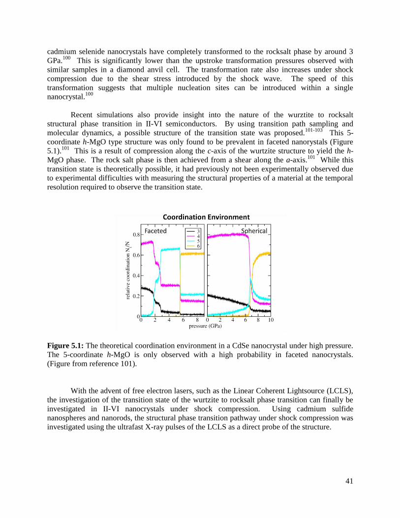
41
cadmium selenide nanocrystals have completely transformed to the rocksalt phase by around 3
GPa.100
This is significantly lower than the upstroke transformation pressures observed with
similar samples in a diamond anvil cell. The transformation rate also increases under shock
compression due to the shear stress introduced by the shock wave. The speed of this
transformation suggests that multiple nucleation sites can be introduced within a single
nanocrystal.100
Recent simulations also provide insight into the nature of the wurztite to rocksalt
structural phase transition in II-VI semiconductors. By using transition path sampling and
molecular dynamics, a possible structure of the transition state was proposed.101-103
This 5-
coordinate h-MgO type structure was only found to be prevalent in faceted nanorystals (Figure
5.1).101
This is a result of compression along the c-axis of the wurtzite structure to yield the h-
MgO phase. The rock salt phase is then achieved from a shear along the a-axis.101
While this
transition state is theoretically possible, it had previously not been experimentally observed due
to experimental difficulties with measuring the structural properties of a material at the temporal
resolution required to observe the transition state.
Figure 5.1: The theoretical coordination environment in a CdSe nanocrystal under high pressure.
The 5-coordinate h-MgO is only observed with a high probability in faceted nanocrystals.
(Figure from reference 101).
With the advent of free electron lasers, such as the Linear Coherent Lightsource (LCLS),
the investigation of the transition state of the wurtzite to rocksalt phase transition can finally be
investigated in II-VI nanocrystals under shock compression. Using cadmium sulfide
nanospheres and nanorods, the structural phase transition pathway under shock compression was
investigated using the ultrafast X-ray pulses of the LCLS as a direct probe of the structure.
42
5.3 Experimental
5.3.1 Nanoparticle Synthesis
Cadmium sulfide nanodots and nanorods were prepared according to Reference 21.
Reagents: Trioctylphosphine oxide (TOPO, 98%), trioctylphosphine (TOP, 98%), and
tributylphosphine (TBP, 98%) were purchased from STREM. Octadecylphosphonic acid
(ODPA) was purchased from PCI Synthesis. Cadmium oxide (99.998%) was obtained from Alfa
Aesar. Hexamethyldisilathiane ((TMS)2S) was purchased from Fluka. Solvents including
toluene, methanol, acetone, and hexanes were purchased from Sigma-Aldrich. Hexylphosphonic
acid (HPA, 95%) and sulfur (S, 99.99%, sublimed) were also purchased from Sigma-Aldrich.
Caution: (TMS)2S is a highly odorous compound and should be handled with care. TBP is
slightly pyrophoric and should be handled using proper air free techniques.
CdS dots: In a 50 mL 3-neck round bottom flask equipped with a condenser, thermocouple
adapter, stir bar, and septum, 3.299 g of TOPO, 0.603 g of ODPA, and 0.1 g of CdO were
combined. The flask was placed under vacuum and heated to 150 °C for 1 hour. The flask was
then backfilled with argon and heated to 300 °C, until a clear and colorless solution was formed.
In a separate vial, 0.170 g of (TMS)2S and 3 g of TBP were combined inside a glovebox. The
reaction mixture was heated to 320 °C and allowed to stabilize. Then, the (TMS)2S and TBP
solution was quickly injected into the reaction mixture using standard air free handling
techniques. The temperature was then set at 250 °C and allowed to grow for 7 minutes after the
injection. The reaction mixture was cooled to about 70 °C where about 7 mL of toluene was
injected. After cooling to room temperature, the solution was transferred to a vial and brought
into a glovebox for cleaning. A solution of clean particles in toluene was achieved through
repetitive precipitation of the particles with methanol or acetone combined with centrifugation
and redissolution in toluene or hexanes.
CdS seed solution: The solution concentration was determined through UV-vis, using the
equation for the absorption coefficient given in Reference 74. Once the concentration of the
resulting CdS nanoparticle solution was determined, a 400 µM solution of CdS dots in TOP was
made. The appropriate amount of CdS dots was precipitated with MeOH and centrifuged. The
resulting pellet was dissolved in TOP to give a 400 µM solution.
CdS nanorods: Several hours before the reaction was performed, 0.120 g S and 1.5 g TOP were
combined and allowed to stir in a glovebox to form TOP-S. In a 50 mL 3-neck round bottom
flask equipped with a condenser, thermocouple adapter, stir bar, and septum, 3 g of TOPO, 0.290
g ODPA, 0.080 g HPA, and 0.086 g of CdO were combined. The reaction mixture was degassed
at 150 °C for 1 hour. The reaction was then back filled with argon and heated to 350 °C. At 350
°C, 1.5 g of TOP was injected quickly, after which the temperature dropped. In a separate vial,
the TOP-S solution made earlier and 200 µL of the CdS seed solution were combined. The
resulting solution was quickly injected into the reaction mixture once the temperature had
recovered to 350 °C. The reaction was allowed to proceed for 7 minutes after the injection. It
was then cooled to room temperature. About 7 mL of toluene was added to prevent

43
solidification. The reaction was cleaned by repeated precipitation with MeOH, centifugation,
and redissolution in toluene.
The size of the nanoparticles could be controlled by changing various parameters,
including the injection temperature, the amount of cadmium oxide, and the amount of sulfur, as
per Reference 21.
Particles were characterized using X-ray diffraction and transmission electron
microscopy in addition to absorption and fluorescence. X-ray diffraction was performed on a
Bruker AXS D8 Gadds instrument with a Co Kα source. Absorption was collected on a Agilent
8453 UV-vis, while fluorescence was performed on a Horiba Fluorolog. A FEI Tecnai G2 S-
Twin transmission electron microscope operating at 200 kV using a LaB6 filament was used to
image the nanocrystals. Micrographs of the nanodots and nanorods are shown in Figure 5.2.
Figure 5.2: Transmission electron micrographs of cadmium sulfide dots and rods.
5.3.2 Substrate Preparation
Shock wave generation was performed through the rapid ablation of a thin aluminum
layer based on the literature.51-52
The shock substrate consisted of a silicon wafer with a thin
silicon nitride (2 µm thick) window. The silicon was etched to give direct access to the silicon
nitride windows. On top of this, a 250 nm layer of aluminum was vapor deposited.
Polyvinylalcohol (PVA, 1 µm thick ±5%) was spin cast from an aqueous solution to act as a
buffer layer. The polymer was cured at 125 °C for 20 minutes. A toluene solution of
nanocrystals was drop cast on top of the polymer to create a 250 nm layer of sample. A back
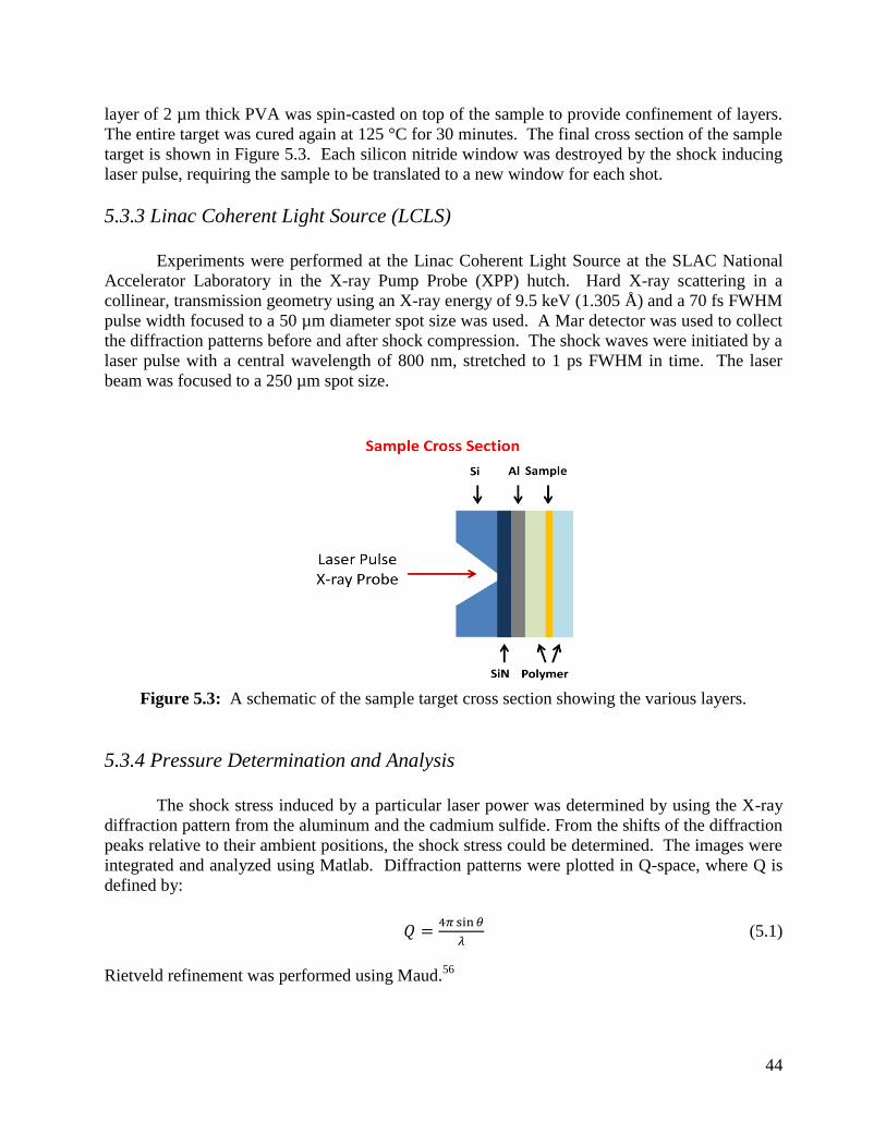
44
layer of 2 µm thick PVA was spin-casted on top of the sample to provide confinement of layers.
The entire target was cured again at 125 °C for 30 minutes. The final cross section of the sample
target is shown in Figure 5.3. Each silicon nitride window was destroyed by the shock inducing
laser pulse, requiring the sample to be translated to a new window for each shot.
5.3.3 Linac Coherent Light Source (LCLS)
Experiments were performed at the Linac Coherent Light Source at the SLAC National
Accelerator Laboratory in the X-ray Pump Probe (XPP) hutch. Hard X-ray scattering in a
collinear, transmission geometry using an X-ray energy of 9.5 keV (1.305 Å) and a 70 fs FWHM
pulse width focused to a 50 µm diameter spot size was used. A Mar detector was used to collect
the diffraction patterns before and after shock compression. The shock waves were initiated by a
laser pulse with a central wavelength of 800 nm, stretched to 1 ps FWHM in time. The laser
beam was focused to a 250 µm spot size.
Figure 5.3: A schematic of the sample target cross section showing the various layers.
5.3.4 Pressure Determination and Analysis
The shock stress induced by a particular laser power was determined by using the X-ray
diffraction pattern from the aluminum and the cadmium sulfide. From the shifts of the diffraction
peaks relative to their ambient positions, the shock stress could be determined. The images were
integrated and analyzed using Matlab. Diffraction patterns were plotted in Q-space, where Q is
defined by:
(5.1)
Rietveld refinement was performed using Maud.56
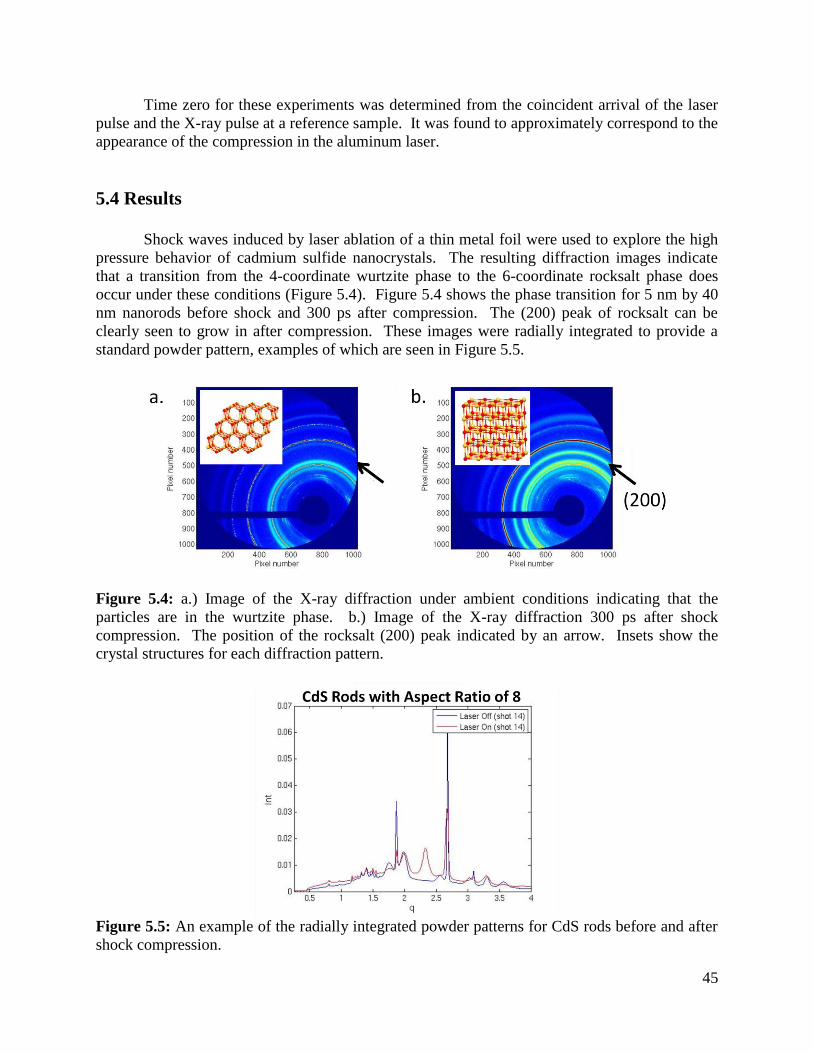
45
Time zero for these experiments was determined from the coincident arrival of the laser
pulse and the X-ray pulse at a reference sample. It was found to approximately correspond to the
appearance of the compression in the aluminum laser.
5.4 Results
Shock waves induced by laser ablation of a thin metal foil were used to explore the high
pressure behavior of cadmium sulfide nanocrystals. The resulting diffraction images indicate
that a transition from the 4-coordinate wurtzite phase to the 6-coordinate rocksalt phase does
occur under these conditions (Figure 5.4). Figure 5.4 shows the phase transition for 5 nm by 40
nm nanorods before shock and 300 ps after compression. The (200) peak of rocksalt can be
clearly seen to grow in after compression. These images were radially integrated to provide a
standard powder pattern, examples of which are seen in Figure 5.5.
Figure 5.4: a.) Image of the X-ray diffraction under ambient conditions indicating that the
particles are in the wurtzite phase. b.) Image of the X-ray diffraction 300 ps after shock
compression. The position of the rocksalt (200) peak indicated by an arrow. Insets show the
crystal structures for each diffraction pattern.
Figure 5.5: An example of the radially integrated powder patterns for CdS rods before and after
shock compression.
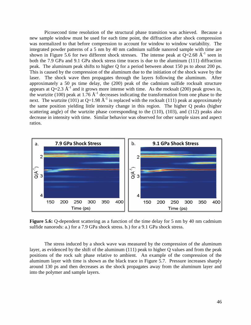
46
Picosecond time resolution of the structural phase transition was achieved. Because a
new sample window must be used for each time point, the diffraction after shock compression
was normalized to that before compression to account for window to window variability. The
integrated powder patterns of a 5 nm by 40 nm cadmium sulfide nanorod sample with time are
shown in Figure 5.6 for two different shock stresses. The intense peak at Q=2.68 Å-1
seen in
both the 7.9 GPa and 9.1 GPa shock stress time traces is due to the aluminum (111) diffraction
peak. The aluminum peak shifts to higher Q for a period between about 150 ps to about 200 ps.
This is caused by the compression of the aluminum due to the initiation of the shock wave by the
laser. The shock wave then propagates through the layers following the aluminum. After
approximately a 50 ps time delay, the (200) peak of the cadmium sulfide rocksalt structure
appears at Q=2.3 Å-1
and it grows more intense with time. As the rocksalt (200) peak grows in,
the wurtzite (100) peak at 1.76 Å-1
decreases indicating the transformation from one phase to the
next. The wurtzite (101) at Q=1.98 Å-1
is replaced with the rocksalt (111) peak at approximately
the same position yielding little intensity change in this region. The higher Q peaks (higher
scattering angle) of the wurtzite phase corresponding to the (110), (103), and (112) peaks also
decrease in intensity with time. Similar behavior was observed for other sample sizes and aspect
ratios.
Figure 5.6: Q-dependent scattering as a function of the time delay for 5 nm by 40 nm cadmium
sulfide nanorods: a.) for a 7.9 GPa shock stress. b.) for a 9.1 GPa shock stress.
The stress induced by a shock wave was measured by the compression of the aluminum
layer, as evidenced by the shift of the aluminum (111) peak to higher Q values and from the peak
positions of the rock salt phase relative to ambient. An example of the compression of the
aluminum layer with time is shown as the black trace in Figure 5.7. Pressure increases sharply
around 130 ps and then decreases as the shock propagates away from the aluminum layer and
into the polymer and sample layers.

47
Figure 5.7: The compression of the aluminum with the time delay is shown in the black trace.
The compression of the cadmium sulfide rocksalt phase is shown in red with the corresponding
time axis on the top. The inset shows the corresponding shifts in Q-space with time.
The diffraction patterns also indicate that the rocksalt phase never relaxes to its ambient
volume in the time frame investigated (Figure 5.7, red trace). The compression of the rocksalt
phase yields a pressure similar to that of the aluminum layer at earlier times, but decays more
slowly.
Shock stress dependent saturation of the rocksalt phase is observed (Figure 5.8). At
pressures less than 4.1 GPa, no conversion to rocksalt is observed. At pressures 6.6 GPa and
higher, the transition to the rock salt phase was observed with the conversion to the new
phaseincreasing with shock stress. At stresses 9.1 GPa and higher, the maximum amount extent
of transformation is reached and saturation behavior is observed.
The diffraction peak position over time provides important insights into the compression
of the material. For instance, at low shock stresses (4.1 GPa), the wurtzite (002) peak shifts to
higher Q, but the wurtzite (100) peak does not shift at all (Figure 5.9a). This shift develops first
as a higher Q shoulder at early times, whereas a single (002) is observed at later times. The
appearance of the shoulder indicates that the shock wave at this time delay is still in the process
of traversing through the sample layer. This implies that part of the sample has been subjected to
a stress while the other part is still ahead of the shock front. The (101) peak of the wurtzite
phase also shifts to higher Q, but to a lesser extent. This indicates aniostopic compression along
the c-axis. A shock stress of 4.1 GPa was not strong enough to generate the rock salt phase. At
higher stresses, different behavior is observed (Figure 5.9b). Higher shock stress induced a
decrease in the intensity of the diffraction peaks, but no corresponding shift to higher Q. This
decrease corresponds directly to the growth of the rocksalt phase, indicating that the wurtzite
phase directly converts to the rocksalt phase.

48
Figure 5.8: The integrated intensity of the (200) peak of the rocksalt phase versus the time delay.
Figure 5.9: Change in the peak shapes and positions at different time delays for a.) a relatively
low shock stress of 4.1 GPa and b.) a higher shock stress of 9.1 GPa.
X-ray diffraction patterns were collected on an ensemble of nanoparticles. This allows
for multiple structural phases to be present in the sample at any one time delay due to the shock
wave width in time and the thickness of the sample layer. Rietveld refinement allows for the
quantitative determination of the phases present in a diffraction pattern. When Rietveld
refinement was performed on the diffractographs, in addition to the aluminum phase and the
wurtzite and rocksalt phases of the cadmium sulfide, a second hexagonal component was found
to be present. This was found to correspond to the 5-coordinate h-MgO structure (P63/mmc). An
example of this at 7.9 GPa is shown in Figure 5.10. At no point in the phase evolution of these
particles is the h-MgO phase the majority phase present.

49
Figure 5.10: Rietveld refinement (black) of cadmium sulfide nanorods under a 7.9 GPa shock
stress, 60 ps after the shock arrival (blue). Four phases were included in the refinement: wurtzite
CdS, rocksalt CdS, h-MgO CdS, and cubic aluminum. The bottom plot shows the residuals.
5.5 Discussion
The timescale for the transformation of these nanoparticles from the wurtzite to the
rocksalt phase is consistent with that predicted by simulations.61
A 4 nm nanodot should
transform in 7-10 ps, while the 5 nm by 40 nm nanorods investigated should transform in 40-80
ps according to simulations. The time range for the transformation of the nanorods depends
where nucleation happens along the rod and the number of nucleation events in a single rod. A
shock wave travelling at 5 nm/ps should traverse the entire sample layer (250 nm) in about 50 ps.
This will convolute the experimentally determined transformation time making an exact
timescale for the conversion to rocksalt in an individual particle impossible to calculate, although
it can be said that the timescale observed for transformation is consistent with the theory.
The phase transition from wurtzite to rocksalt under shock compression happens at
pressures lower than the same transition under hydrostatic pressure conditions (Figure 5.8).6-8
This is a commonly observed trend in materials and is attributed to shear forces that are present
in a shock wave.50
Interestingly, the rocksalt phase produced by shock compression has a
volume smaller than that under ambient conditions, indicating that it is compressed (Figure 5.7).
The rocksalt phase also persists for the timeframe of the measurement (8 ns); it does not
transform back to the wurtzite phase, but the lattice parameters do relax slowly (Figure 5.11).
This is thought to occur due to this phase transition having a very wide hysteresis curve for
nanocrystals, making the existence of the rocksalt phase at pressures well below the
thermodynamic phase transition pressure possible.6-8
The rocksalt particles are kinetically
trapped until the barrier to the nucleation of the wurtzite phase can be overcome.33
Larger
nanoparticles have been shown to be metastable in the rocksalt phase at ambient pressures.8
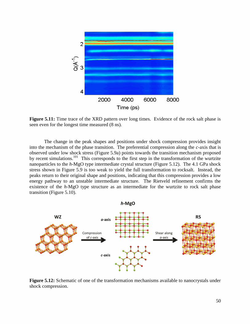
50
Figure 5.11: Time trace of the XRD pattern over long times. Evidence of the rock salt phase is
seen even for the longest time measured (8 ns).
The change in the peak shapes and positions under shock compression provides insight
into the mechanism of the phase transition. The preferential compression along the c-axis that is
observed under low shock stress (Figure 5.9a) points towards the transition mechanism proposed
by recent simulations.101
This corresponds to the first step in the transformation of the wurtzite
nanoparticles to the h-MgO type intermediate crystal structure (Figure 5.12). The 4.1 GPa shock
stress shown in Figure 5.9 is too weak to yield the full transformation to rocksalt. Instead, the
peaks return to their original shape and positions, indicating that this compression provides a low
energy pathway to an unstable intermediate structure. The Rietveld refinement confirms the
existence of the h-MgO type structure as an intermediate for the wurtzite to rock salt phase
transition (Figure 5.10).
Figure 5.12: Schematic of one of the transformation mechanisms available to nanocrystals under
shock compression.

51
Given the speed of the shock wave through the material (approximately 5 nm/ps) and
assuming a single nucleation event per nanocrystal, part of the sample should be in the process of
transforming while it was still being probed. While the Rietveld refinement confirms that some
of the particles in the ensemble have a h-MgO structure, it also indicates this phase never
becomes the majority constituent. This opens the door for an additional mechanism that occurs
concurrently with the h-MgO intermediate that directly transforms the wurtzite to the rocksalt
phase. This is supported by the absence of the preferred compression along the c-axis at higher
shock pressures (Figure 5.9b). The absence of the intermediate also indicates that the activation
energy for the transformation has been reduced under high shock stress allowing for the direct
conversion from one phase to the next at a faster rate than those observed under hydrostatic
conditions. This direct pathway has been suggested to occur for particles that have a disordered
surface;101
well faceted particles are thought to undergo the transformation through the
intermediate phase.101
The rapid increase in pressure and the uniaxial nature of the stress in
shock waves may cause a disruption of the surface of the nanocrystals, leading to the direct
pathway to be preferred at higher shock stress.
5.6 Conclusions
For the first time, the h-MgO type intermediate structure of the wurtzite to rocksalt phase
transition in cadmium sulfide has been observed. This provides the first experimental evidence
supporting the theoretical intermediate phase. In addition, while this phase is present, it does not
represent the only pathway available for the structural phase transformation under shock
compression. A direct pathway from the wurtzite to the rocksalt phase also exists at high shock
stress. The shear component of the shock wave catalyzes the phase transition, allowing it to
occur at stresses significantly lower than those observed under hydrostatic pressure conditions.
The reduction of the over-pressurization needed for the phase transition to occur indicates a
decrease in the height of the activation barrier. The rapid nature of shock compression and the
introduction of shear into the system open the door for investigating not only the mechanism of
these structural phase transitions, but also the possible discovery of new structural phases in
nanomaterials.
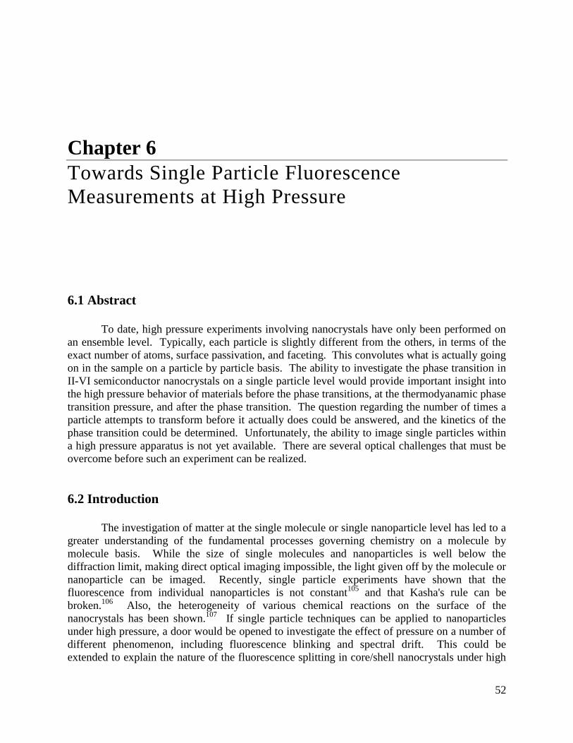
52
Chapter 6
Towards Single Particle Fluorescence
Measurements at High Pressure
6.1 Abstract
To date, high pressure experiments involving nanocrystals have only been performed on
an ensemble level. Typically, each particle is slightly different from the others, in terms of the
exact number of atoms, surface passivation, and faceting. This convolutes what is actually going
on in the sample on a particle by particle basis. The ability to investigate the phase transition in
II-VI semiconductor nanocrystals on a single particle level would provide important insight into
the high pressure behavior of materials before the phase transitions, at the thermodyanamic phase
transition pressure, and after the phase transition. The question regarding the number of times a
particle attempts to transform before it actually does could be answered, and the kinetics of the
phase transition could be determined. Unfortunately, the ability to image single particles within
a high pressure apparatus is not yet available. There are several optical challenges that must be
overcome before such an experiment can be realized.
6.2 Introduction
The investigation of matter at the single molecule or single nanoparticle level has led to a
greater understanding of the fundamental processes governing chemistry on a molecule by
molecule basis. While the size of single molecules and nanoparticles is well below the
diffraction limit, making direct optical imaging impossible, the light given off by the molecule or
nanoparticle can be imaged. Recently, single particle experiments have shown that the
fluorescence from individual nanoparticles is not constant105
and that Kasha's rule can be
broken.106
Also, the heterogeneity of various chemical reactions on the surface of the
nanocrystals has been shown.107
If single particle techniques can be applied to nanoparticles
under high pressure, a door would be opened to investigate the effect of pressure on a number of
different phenomenon, including fluorescence blinking and spectral drift. This could be
extended to explain the nature of the fluorescence splitting in core/shell nanocrystals under high

53
pressure, as it is not known if this is an ensemble effect or if each particle is emitting a number of
different states that average to the observe fluorescence spectrum. In addition, the nature of a
structural phase transition could be investigated on a particle by particle basis giving insight into
the kinetics of the phase transition in II-VI semiconductors. This could include investigating the
number of times the phase transition is attempted, the pressure corresponding to the
thermodynamic equilibrium, and the rate at which the nanocrystal converts from one phase to the
next. These properties are blurred by measurements done on an ensemble level.
To date, the only experiment that makes an attempt to investigate nanoscale single
particles is from Mao et al.108
This study looked at NbSe3 nanobelts at pressures up to 20 GPa.
The nanobelts studied are huge compared to the regime where size dependent behavior has been
observed.
To achieve the ability to perform single particle optical studies under high pressure, a
multitude of obstacles involving the optics of the system, the diamond anvil cell, and the sample
must first be overcome.
6.3 The Diamond Anvil Cell
6.3.1 Optical Problems with the Diamond Anvil Cell
One of the major problems associated with measuring the fluorescence of single
nanoparticles in a diamond anvil cell is the presence of the diamond itself. Diamond has a high
index of refraction of 2.42. In addition, the reflection loss through the diamond when the four
diamond surfaces present in the diamond anvil cell are taken into account is roughly 50%.29
If
the excitation source and the particle fluorescence is bright enough this loss should not play a
limiting role in the optics of the system. The major problem associated with imaging in a
diamond anvil cell can most easily be explained through the treatment of the diamond as a plane
parallel plate.29
For a parallel plate in a collimated beam, no aberrations are introduced into the
system. However, when the same parallel plate is placed in a converging or diverging beam, a
series of aberrations including chromatic, spherical, and astigmatism are introduced. For the
purposes of imaging single particles, the spherical aberration shall be discussed in detail.
When a plane parallel plate is inserted into a converging or diverging beam, the beam is
displaced longitudinally due to change in index relative to air (Figure 6.1). The longitudinal
displacement, Δp, can be calculated from the equation:
, (6.1)
where N is the index of refraction and t is the thickness of the plate.109
For a diamond with a
thickness of 1.8 mm (the thickness of some of the diamonds used here), the longitudinal
displacement of the image is 1.06 mm. This equation only applies to the paraxial region.
Outside the paraxial region the longitudinal displacement, Δm, is:

54
, (6.2)
where f/# is the f-number.109
Assuming a 50 x objective with a numerical aperture of 0.55, Δm
can be approximated as 1.16 mm for a diamond anvil. From these values, the longitudinal
spherical aberration, defined as the difference between Δm and Δp, for the diamond anvil is 0.1
mm. The blur diameter for this spherical aberration, defined as:110
. (6.3)
For a diamond anvil and the above described objective, the blur diameter of the spherical
aberration is 0.026 mm. This is significant given the size of the point source that is being
imaged.
Figure 6.1: A plane parallel plate in a converging beam. The beam is displaced by a distance
of Δ.
Typically, the spherical aberration can be corrected for through the use a microscope
objective with a correction collar. Unfortunately, for the case of the diamond anvil, the spherical
aberration is too great to be completely corrected through this method particularly given the
constraints placed on the objective by the use of a diamond anvil cell. The working distance
required by the use of the diamond anvil cell limits the number of objectives available for this
purpose to only a handful, none of which have a correction collar for the correction of spherical
aberration.
The spherical aberration and loss of signal due to the presence of the diamonds pose a
significant challenge in imaging signal nanoparticle fluorescence and must be overcome for these
studies to be successful.

55
6.3.2 Possible Solution: The Mini-Diamond and Diamond Backing Plate
Configuration
By examining the equations defining the spherical aberration above, the simplest way to
reduce the aberrations caused by having a thick diamond substrate may be to reduce the amount
of diamond through which the light has to travel. One method to achieve this is the use of a
perforated diamond anvil as a backing plate (Figure 6.2). In a perforated diamond anvil, the
point has been lapped off to a significant extent and a hole has been milled either part way
through the diamond or the entirely though the diamond.111-112
The perforation can be
cylindrical or conical. This reduces the amount of diamond through with the excitation source
and the resulting image has to pass. For the case of single particle imaging, a partially perforated
diamond anvil cannot be used as a backing plate or as an anvil in its own right because the inner
surface is not polished.111
This would lead to the scattering of the light as it passed through this
interface and additional blurring of the image.
Figure 6.2: Schematic of a perforated diamond anvil that can be used as a diamond backing
plate: a.) the side view of the anvil b.) the top view showing the hole that has been drilled
through the entire diamond.
Because of the imaging issues that would be experienced if a partially perforated
diamond anvil was used, a fully drilled anvil must be used for imaging single particle
fluorescence. In this case, the fully perforated diamond anvil will actually serve as a backing
plate for a miniature diamond anvil to be seated upon (Figure 6.3). Such a configuration has
been used to successfully achieve high pressure in the literature.111-112
For a miniature diamond
anvil with a thickness of 0.64 mm, Δp=0.38 mm and Δm=0.41mm (assuming the 50x, NA=0.55

56
objective discussed above), giving a longitudinal spherical aberration of only 0.03 mm and a blur
diameter of 0.009 mm for the diamond. In comparison, a 1 mm thick glass slide with an index of
refraction of 1.52, through which the fluorescence of single nanoparticles can be imaged (albeit
they are a bit blurry), has a longitudinal spherical aberration of 0.07 mm with a blur diameter of
0.015 mm. Given this, single particles should be able to be imaged through a miniature anvil.
Unfortunately, this rough calculation does not account for defects within the diamond itself,
which cause a fluorescent background that is high enough to wash out the fluorescence from the
individual particles. Even diamonds that were supposed to possess low fluorescence according
to the supplier had too large of a background. Both type I and type II diamonds can be classified
as low fuorescence.29
Ultra-low fuorescence is needed for this application.
Figure 6.3: Diagram showing miniature diamond anvils mounted on diamond backing plate.
The diamond backing plates are then secured onto metal backing plates before being put into a
diamond anvil cell.
Unless diamond suppliers allow us to screen their diamonds for the ultra-low levels of
fluorescence that are required for this experiment, the fluorescence of the diamonds limits the
feasibility of this configuration for high pressure single particle imaging.
6.3.3 Possible Solution: The Sapphire Cell and the Hybrid Diamond-Sapphire Cell
From the spherical aberration equations, the reduction of the index of refraction will also
result in the reduction of the aberration. Another material that is commonly used for anvil
construction in high pressure experiments up to about 10 GPa is sapphire.113-114
Sapphire has an
index of refraction of 1.78. Sapphire is not as hard as diamond, but its mechanical properties are
amenable to the lower part of the pressure scale.113
Because it is not as hard, the machining of
sapphire into various shapes, including lenses, is significantly easier. Several geometries of
sapphire cells have been used, including one made from truncated ball lenses (Figure 6.4a).113

57
Because sapphire is relatively easy to machine, cells like that shown in Figure 6.4b could
theoretically be designed. This configuration, when properly designed, allows for the use of the
anvils as solid immersion lenses in addition to pressure exerting apparatuses. A solid immersion
lens operates on the same principles that govern oil immersion microscopy.115
For an oil
immersion lens, oil is placed between the lens and the sample. This increases the index of
refraction between the two materials, which in turn increases the numerical aperture of the
system. A higher numerical aperture implies better optical resolution and collection efficiency.
A hemispherical solid immersion lens works on the same principle, but using a high index of
refraction solid, such as sapphire, instead of the immersion oil. The hemisphere increases the
magnification of the objective lens being utilized and the numerical aperture by a factor of the
index of refraction.116-117
The image passing through the center of the solid immersion lens is
free of aberration, but the aberration increases with the angle of the off-axis light.117
In addition,
the hemispherical lens does not possess longitudinal chromatic aberration, only a very small
lateral chromatic aberration. Other geometries, such as Weirstrass solid immersion lenses could
possibly be used, but they do not provide the same advantages to our application as does a
hemispherical solid immersion lens.117
Figure 6.4: Diagrams of two sapphire anvil cells. a.) A truncated sapphire ball cell from
Reference 113. b.) A theoretical sapphire cell in which the anvil could also be used as a solid
immersion lens (from Reference 44).
Figure 6.5: Schematic of a hybrid sapphire and diamond anvil cell.

58
Given the increase in collection efficiency and the reduction of the spherical aberration in
the center of a hemispherical solid immersion lens, such a lens would be ideal for imaging inside
a high pressure cell. Unfortunately, a supplier for the sapphires shown in the configuration
shown in Figure 6.4b could not be found. However, sapphire ball lenses and hemispherical
lenses are prevalent. A design for a high pressure cell consisting of one diamond anvil and one
sapphire hemisphere was proposed (Figure 6.5).118
This cell would allowed for particles located
on the surface of the sapphire hemisphere to be imaged under high pressure, provided that the
hemisphere could support the pressures required.
Before the cell could be subjected to pressure, the ability to image single nanoparticle
fluorescence on top of the solid immersion lens had to be determined. Unfortunately, the
sapphire half ball lenses purchased from several suppliers show similarly high backgrounds and
contamination from Cr3+
doping and defect states (Figure 6.6).44,118
This background could be
reduced, but not eliminated, from the sapphire by annealing at high temperatures. This high
background prevented the observation of single particle fluorescence even if the high intensity
higher wavelengths were filtered out through the use of band pass filters.
Figure 6.6: Fluorescence spectra of two different sapphires from two different suppliers. The
ruby peak around 690 nm that is due to Cr3+
doping of the sapphire.
6.3.4 Possible Solution: Correction Outside of the High Pressure Apparatus
In many cases, spherical aberration can be corrected for by the simple addition of an optic
with a longitudinal displacement in the opposite direction into the image path. For instance, a
convex, or converging, lens will have an undercorrected (negative) spherical aberration, opposite
of that of a plane parallel plate.119
A concave, or diverging, lens will have an overcorrected
(positive) spherical aberration.119
A convex or plano-convex lens could therefore be used to
correct for the positive spherical aberration introduced by a plane parallel plate. Many types of
aberration come into play when trying to calculate the type of lens that needs to be used, making
such calculations difficult. For the diamond anvil cell, several commercially available lens
combinations were placed between the microscope and the spectrometer in an attempt to correct
the spherical aberration. None of the commercially available lenses in the standard lens kit that

59
were tested corrected for the spherical aberration adequately. A custom made lens or series of
lenses could be designed for this purpose in the future.
6.4 The Sample
6.4.1 Loading Difficulties
If the optical challenges could be overcome, there would still be several sample
difficulties that would need to be surmounted. The first of these difficulties is the convenience
of having a planar sample for single particle imaging. A 2-dimersional sample, such as that
created by a dilute solution drop casted onto a cover slip, makes finding the individual particles,
and subsequently imaging them, a lot easier. A 3-dimensional sample poses challenges
stemming from an increase in the background due to out of focus particles and simply being able
to find and focus on individual particles. Background from the surrounding medium will also
contribute to the signal and pose additional difficulty. This could simply be overcome by drop
casting a dilute sample of the particles on the surface of the diamond before loading with a
pressure transmitting medium that the particles are not soluble in. Unfortunately, such a
technique, while simple, may introduce a non-hydrostatic environment around the particle as it
would no longer be completely surrounded by the pressure transmitting medium. An additional
method that may overcome these issues, would be to embed the particles in a glass that is not
soluble in the pressure transmitting medium. While this would probably cause an increase in the
background, reducing the signal to noise, it would provide a hydrostatic environment if the glass
was chosen carefully.
6.4.2 The Nanocrystals
The second obstacle to be overcome is the sample itself. It would be ideal to have a
sample that undergoes an abrupt shift in emission wavelength from one color in the visible
spectrum to another during a phase transition. Unfortunately, when undergoing a structural
phase transition from the wurtzite or zinc blende phase to the rocksalt phase, many II-VI
semiconductors actually go from a system with bright fluorescence to one that does not
fluoresce. This is because the low pressure wurtzite and zinc blende phases are direct band gap
semiconductors in which fluorescence is allowed, but the high pressure rocksalt phase is an
indirect band gap semiconductor in which fluorescence is forbidden process. This means that the
particles would be going from a bright "on" state to a dark "off" state. This process would then
be convoluted with the blinking phenomenon that has already been observed for single II-VI
nanocrystals. If the II-VI semiconductor system is to be used for these experiments, then the
blinking of the particles must be suppressed.
One method of suppressing blinking in II-VI nanoparticles is to deposit a thick epitaxial
shell made of cadmium sulfide around a cadmium selenide core.120-121
This prevents
fluorescence loss by reducing the number of surface traps and confining the hole to the cadmium
selenide core.120-121
This reduces the blinking frequency, allowing for particles with long "on"
times and high quantum yields to be synthesized. A synthesis of these CdSe/CdS core/giant shell

60
particles based on Reference 121, with a few changes is described below using the successive ion
layer absorption and reaction (SILAR) method.
6.4.2.1 Synthesis
Reagents: Cadmium oxide (CdO, 99.99%), oleic acid (70% tech grade), selenium powder (-100
mesh), oleylamine (90%), and sulfur (99.5%) were purchased from Sigma-Aldrich. Octadecene
(ODE, 90%) was purchased from Lancaster. Trioctylphosphine (TOP, 98%) was purchased
from STREM. Tetradecylphosphonic acid was purchased from PCI Synthesis. Common
solvents such as methanol, isopropanol, acetone, and hexane were also purchased from Sigma-
Aldrich
CdSe Quantum Dots: Before the reaction was to be performed a Cd(oleate)2 (0.5 M in oleic
acid) was prepared by heating 0.145 g CdO in 2 mL oleic acid to 170 °C under flowing Ar. The
precursor solution was then cooled to room temperature and stored under Ar. The TOP-Se
precursor was synthesized by stirring 158 mg of Se powder and 2 mL of TOP overnight in the
glovebox. In a 25 mL 3-neck round bottom flask equipped with a condenser, thermocouple
adapter, septum, and stir bar, 0.2 mL of the Cd(oleate)2 precursor and 3 mL of ODE were
combined and heated to 70 °C under vacuum for 1 hour. The flask was then backfilled with
argon and heated to 240 °C. In a separate flask (equipped the same as above), 1.5 mL of the
TOP-Se precursor, 1.5 mL of oleylamine, and 1 g of TDPA were combined and heated to 110 °C
under argon until the solution turned clear. The TOP:Se solution was then injected into the flask
containing the cadmium mixture using a glass syringe with a wide bore needle. The temperature
was lowered to 200 °C and grown for 50 seconds after the injection. The solution changed
colors from colorless to yellow, then orange to red. The solution was cooled to 60 °C and 5 mL
of hexane was added before the solution cooled to room temperature. The cleaning of the
nanocrystals consisted of a two step process. In the first step, the reaction mixture was layered
with MeOH. The top MeOH layer was removed, and the process was repeated once. In step
two, isopropanol was added to the colored layer and the solution was centrifuged to yield a pellet
of nanocrystals. The pellet was dissolved in hexane. The solution was repeatedly precipitated
and re-dissolved until a clear, clean solution of nanoparticles in hexane was obtained. The
particle size was characterized by absorption and transmission electron microscopy. The
solution concentration was determined from the absorption coefficients in Reference 74.
SILAR Precursors: The cadmium precursor was synthesized in a 25 mL 3-neck flask by
combining 256 mg of CdO, 4.38 mL oleic acid, and 5.62 mL ODE and heating the mixture to
250 °C under Ar until the CdO was completely reacted. The mixture was then diluted to a 0.1 M
concentration in Cd by the addition of ODE. The sulfur precursor was synthesized in a 25 mL 3-
neck flask by combining 64 mg of S and 10 mL ODE and heating to 200 °C under Ar under the
sulfur was dissolved. The sulfur solution was then diluted to a concentration of 0.1 M in S by
dilution with ODE.
Calculations for the Addition of the Shell Material: The amount of the cadmium and sulfur
precursors was determined by first determining the surface area of the particles. Then, given the
thickness of a single monolayer of CdS and its density, the amount of each precursor could be
calculated on a per monolayer basis.

61
CdSe/CdS Core/Shell Particles: In a 50 mL 3-neck round bottom flask equipped with a
condenser, thermal couple adapter, stir bar, and septum 2 mL oleylamine, 4 mL ODE, and
approximately 8.13×10¹⁶
CdSe nanoparticles (solution in hexane) were combined. The hexane
was removed under vacuum. When the majority of the hexane had been removed, the solution
was heated to 70 °C and degassed under vacuum for an additional 30 minutes to remove any
remaining hexane and air. The reaction mixture was then backfilled with argon. The stock
cadmium precursor (enough for a single monolayer) was added dropwise to the reaction mixture.
The temperature was then increased to 230 °C. Ten minutes after the desired temperature was
achieved, the same volume of the sulfur precursor was added dropwise. The temperature was
then increased to 240 °C. The dropwise injections of the cadmium and sulfur were alternated
every 10 minutes until the desired shell thickness was achieved, ending on cadmium. Twenty
minutes after the final injection, the reaction was cooled to room temperature. Afterwards, ~5
mL of hexane was added and the reaction mixture was transferred to the glovebox. Particles
were cleaned using the same process as that of the CdSe dots. Self-nucleated CdS particles were
removed through additional layering with methanol and centrifugation. The amount of CdS was
monitored through fluorescence.
Characterization: Particles were characterized using transmission electron microscopy in
addition to absorption and fluorescence. Absorption was collected on an Agilent 8453 UV-vis,
while fluorescence was performed on a Horiba Fluorolog. A FEI Tecnai G2 S-Twin transmission
electron microscope operating at 200 kV using a LaB6 filament was used to image the
nanocrystals.
6.5 The Fluorescence Microscope
The configuration of the fluorescence microscope for performing single particle
experiments at high pressure is perhaps the easiest challenge to overcome. Single particle
experiments are now common place and adapting a microscope to accommodate a diamond anvil
cell, while maintaining the ability to image the emission from a single particle, is not terribly
difficult (Figure 6.7). In this case, a Lexel 95 Ar+ Ion laser set to emit at 488nm was used as an
excitation source. It was passed through a spatial filter to clean up the beam shape and a laser
line filter to exclude any other wavelengths that may have escaped from the laser. A focusing
lens before the back of the microscope can be used to control the beam size. For single particle
imaging inside a diamond anvil cell, a 50× Zeiss LD EC Epiplan-Neofluar objective with a
NA=0.55 and a working distance of 9 mm was chosen. This objective provides the working
distance required to accommodate a small diamond anvil cell, in addition to the magnification
and numerical aperture required to image single particle fluorescence with good signal to noise.
A Zeiss Axiovert inverted microscope was chosen as it provided plenty of space on the stage to
accommodate the diamond anvil cell. The fluorescence spectrum was dispersed by an Acton
SpectroPro 300i and collected by a Princeton Instruments Spec-10 liquid nitrogen cooled
camera. This configuration has proven to be adequate for the imaging and spectroscopy of single
nanocrystals.
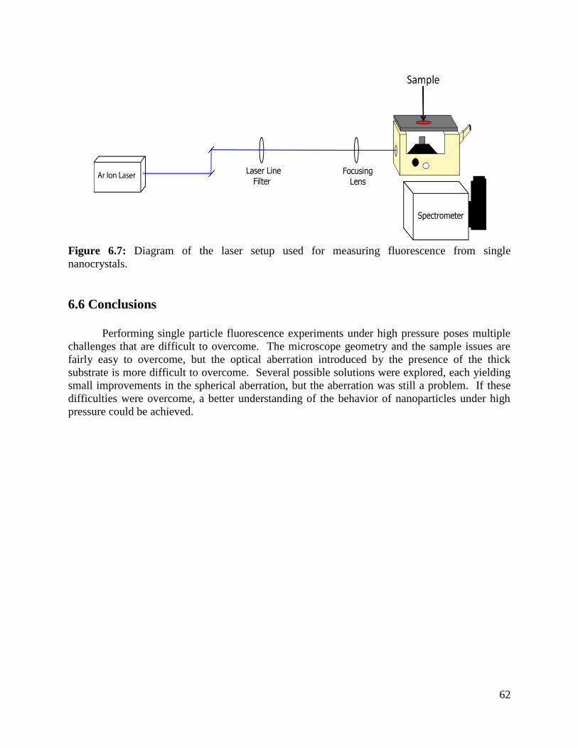
62
Figure 6.7: Diagram of the laser setup used for measuring fluorescence from single
nanocrystals.
6.6 Conclusions
Performing single particle fluorescence experiments under high pressure poses multiple
challenges that are difficult to overcome. The microscope geometry and the sample issues are
fairly easy to overcome, but the optical aberration introduced by the presence of the thick
substrate is more difficult to overcome. Several possible solutions were explored, each yielding
small improvements in the spherical aberration, but the aberration was still a problem. If these
difficulties were overcome, a better understanding of the behavior of nanoparticles under high
pressure could be achieved.

63
Chapter 7
Detection of Cellular Forces Using a Nanocrystal
Sensor
7.1 Abstract
The photoluminescence of cadmium selenide/cadmium sulfide core/shell nanocrystal
tetrapods has proven to be extremely sensitive to minute forces. Once calibrated, these particles
have been shown to be able to correctly map out forces in polymer fibers under tensile stress. In
this work, tetrapod nanocrystals were shown to provide a viable route towards imaging forces in
biological systems. The nanocrystals provide the system with spatial and temporal resolution.
By covalently linking hydrophilically modified tetrapods to a glass substrate, the tetrapod
fluorescence can be used to monitor forces in biological systems. An acousto-optic tunable filter
was necessary on the detection side of the microscope to impart the measurement with the
temporal, spatial, and spectral resolution needed to map out the forces exerted on a substrate by
the cultured cells. HL-1 rat cardiomyocytes were used as a trial system, as they exert a dynamic
force on their surroundings as they beat. From the fluorescence of the tetrapod substrate, the
force exerted by the HL-1 cardiomyocytes was determined to be 0.7 nN, which agrees with
values determined through other experimental methods.
7.2 Introduction
7.2.1 Tetrapod Nanocrystals
The colloidal synthesis of nanocrystals has evolved such that shaped controlled
heterostructures can be easily achieved.22
The cadmium selenide- cadmium sulfide (CdSe/CdS)
system is a perfect example of this control. CdSe/CdS heterostructure nanocrystals can be
synthesized as core-shell dots, rods, or tetrapods.22,121
Tetrapods are a branched nanostructure
consisting of four wurtzite CdS arms grown epitaxially from the (111) facet of a zinc blende
CdSe dot (Figure 7.1).
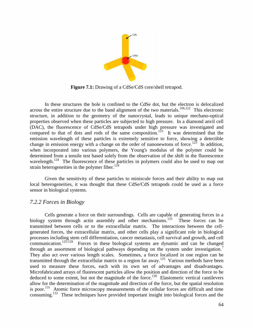
64
Figure 7.1: Drawing of a CdSe/CdS core/shell tetrapod.
In these structures the hole is confined to the CdSe dot, but the electron is delocalized
across the entire structure due to the band alignment of the two materials.106,122
This electronic
structure, in addition to the geometry of the nanocrystal, leads to unique mechano-optical
properties observed when these particles are subjected to high pressure. In a diamond anvil cell
(DAC), the fluorescence of CdSe/CdS tetrapods under high pressure was investigated and
compared to that of dots and rods of the same composition.123
It was determined that the
emission wavelength of these particles is extremely sensitive to force, showing a detectible
change in emission energy with a change on the order of nanonewtons of force.123
In addition,
when incorporated into various polymers, the Young's modulus of the polymer could be
determined from a tensile test based solely from the observation of the shift in the fluorescence
wavelength.124
The fluorescence of these particles in polymers could also be used to map out
strain heterogeneities in the polymer fiber.124
Given the sensitivity of these particles to miniscule forces and their ability to map out
local heterogeneities, it was thought that these CdSe/CdS tetrapods could be used as a force
sensor in biological systems.
7.2.2 Forces in Biology
Cells generate a force on their surroundings. Cells are capable of generating forces in a
biology system through actin assembly and other mechanisms.125
These forces can be
transmitted between cells or to the extracellular matrix. The interactions between the cell-
generated forces, the extracellular matrix, and other cells play a significant role in biological
processes including stem cell differentiation, cancer metastasis, cell survival and growth, and cell
communication.125-129
Forces in these biological systems are dynamic and can be changed
through an assortment of biological pathways depending on the system under investigation.7
They also act over various length scales. Sometimes, a force localized in one region can be
transmitted through the extracellular matrix to a region far away.125
Various methods have been
used to measure these forces, each with its own set of advantages and disadvantages.
Microfabricated arrays of fluorescent particles allow the position and direction of the force to be
deduced to some extent, but not the magnitude of the force.130
Elastomeric vertical cantilevers
allow for the determination of the magnitude and direction of the force, but the spatial resolution
is poor.131
Atomic force microscopy measurements of the cellular forces are difficult and time
consuming.132
These techniques have provided important insight into biological forces and the

65
mechanical properties of cells and tissues, but these forces occur with a spatial resolution much
smaller than the current state of the art resolution allows.
By using the fluorescence of tetrapod nanocrystals as a force sensor, it is possible to
monitor the periodic forces generated by HL-1 rat cardiomyocytes with simultaneous spatial,
temporal, and spectral resolution. This is an important step towards monitoring cell-generated
forces with submicron resolution.
7.3 Experimental
7.3.1 Synthesis
7.3.1.1 Synthesis of CdSe/CdS Tetrapod Nanocrystals
CdSe/CdS tetrapod nanocrystals were synthesized from a two part literature preparation
as follows.22
Reagents: Cadmium oxide (CdO, 99.999%) and 1-octadecence (ODE, 90%) were purchased
from Alfa Aesar. Myristic acid (99%), selenium powder (-100 mesh, 99.99%), oleic acid (90%),
oleylamine (70%), propylphosphonic acid (PPA, 95%), diaminohexane (98%), (1-ethyl-3-(3-
dimethylaminopropyl)carbodiimide hydrochloride (EDC), N-hydroxysulfosuccinide (sulfo-
NHS), hydroxylamine (50 wt%), poly(maleic anhydride alt-1-tetradecene) (polyMAAT) and
sulfur (S, 99%) were purchased from Sigma-Aldrich. ACS grade methanol, acetone, hexane,
chloroform, and toluene were also purchased from Sigma-Aldrich. Trioctylphosphine oxide
(TOPO, 99%) and trioctylphosphine (TOP, 98%) were purchased from STREM.
Octadecylphosphonic acid (ODPA) was purchased from PCI Synthesis. Dulbecco's phosphate
buffered saline (DPBS, 1×) with no cadmium chloride and no magnesium chloride was
purchased from Gibco. Amine coated glass coverslips were purchased as a special order from
ArrayIt. All chemicals were used as received with no purification.
Zinc Blende CdSe Dots: In a 100 mL 3-neck roundbottom flask equipped with a condenser,
thermocouple adapter, septum, and magnetic stir bar, 0.077 g of CdO, 0.29 g of myristic acid,
and 5 mL of ODE were combined and heated to 250 °C under argon. When the solution was
golden in color it was immediately cool down to approximately 40 °C, at which point 32 mL of
ODE was added to the reaction vessel. The solution was heated to 80 °C under vacuum for 1
hour. In a separate vial, 0.1 mL oleic acid, 1 mL oleylamine, and 4 mL ODE were combined and
degassed under vacuum. After 1 hour, the cadmium solution was backfilled with argon and
cooled to room temperature. Selenium powder (0.024g) was added to the reaction mixture
which was promptly heated to 50°C and degassed under vacuum for 10 minutes. The reaction
was once again backfilled with argon and heated to 240 °C. During the heating, the reaction
mixture changed colors from colorless to yellow to orange to red. The oleic acid, oleylamine,
and ODE mixture was added dropwise to the reaction about 3 minutes after the reaction mixture
had reached temperature. The nanocrystals were allowed to grow at 240 °C for 1 hour before
they were cooled to room temperature. Cleaning was performed through successive
centrifugation after precipitation by an anti-solvent (methanol or acetone) and redissolution in
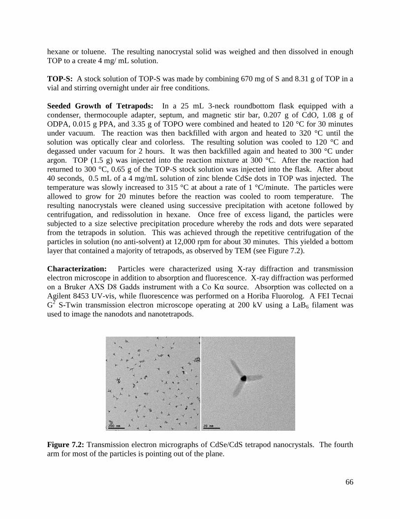
66
hexane or toluene. The resulting nanocrystal solid was weighed and then dissolved in enough
TOP to a create 4 mg/ mL solution.
TOP-S: A stock solution of TOP-S was made by combining 670 mg of S and 8.31 g of TOP in a
vial and stirring overnight under air free conditions.
Seeded Growth of Tetrapods: In a 25 mL 3-neck roundbottom flask equipped with a
condenser, thermocouple adapter, septum, and magnetic stir bar, 0.207 g of CdO, 1.08 g of
ODPA, 0.015 g PPA, and 3.35 g of TOPO were combined and heated to 120 °C for 30 minutes
under vacuum. The reaction was then backfilled with argon and heated to 320 °C until the
solution was optically clear and colorless. The resulting solution was cooled to 120 °C and
degassed under vacuum for 2 hours. It was then backfilled again and heated to 300 °C under
argon. TOP (1.5 g) was injected into the reaction mixture at 300 °C. After the reaction had
returned to 300 °C, 0.65 g of the TOP-S stock solution was injected into the flask. After about
40 seconds, 0.5 mL of a 4 mg/mL solution of zinc blende CdSe dots in TOP was injected. The
temperature was slowly increased to 315 °C at about a rate of 1 °C/minute. The particles were
allowed to grow for 20 minutes before the reaction was cooled to room temperature. The
resulting nanocrystals were cleaned using successive precipitation with acetone followed by
centrifugation, and redissolution in hexane. Once free of excess ligand, the particles were
subjected to a size selective precipitation procedure whereby the rods and dots were separated
from the tetrapods in solution. This was achieved through the repetitive centrifugation of the
particles in solution (no anti-solvent) at 12,000 rpm for about 30 minutes. This yielded a bottom
layer that contained a majority of tetrapods, as observed by TEM (see Figure 7.2).
Characterization: Particles were characterized using X-ray diffraction and transmission
electron microscope in addition to absorption and fluorescence. X-ray diffraction was performed
on a Bruker AXS D8 Gadds instrument with a Co Kα source. Absorption was collected on a
Agilent 8453 UV-vis, while fluorescence was performed on a Horiba Fluorolog. A FEI Tecnai
G2 S-Twin transmission electron microscope operating at 200 kV using a LaB6 filament was
used to image the nanodots and nanotetrapods.
Figure 7.2: Transmission electron micrographs of CdSe/CdS tetrapod nanocrystals. The fourth
arm for most of the particles is pointing out of the plane.

67
Polymer Wrapping: The native ligands of the tetrapods are hydrophobic, but to be
incorporated into a biologically relevant system the particles need to be hydrophilic. In order for
this to be achieved, a simple polymer wrapping technique was employed.133
Briefly, 1 mL of a 1
µM solution of tetrapods in chloroform was prepared. Then, a second solution of 105 mg of
diaminohexane in 6.3 mL of chloroform was also prepared. A third solution of 27 mg of
poly(MAAT) in 1 mL of chloroform was prepared. The tetrapod solution was combined with the
poly(MAAT) solution and stirred overnight at room temperature. Seventy microliters of the
diaminohexane solution was added to the tetrapod solution. The solution was allowed to stir for
90 minutes before the chloroform was evaporated off. The tetrapods were dissolved in 1x PBS
until the solution was clear. Then, the particles were concentrated using Amicon Ultra 100K
centrifuge filters. The resulting carboxylic acid terminated particles were stable in 1× DPBS
over a period of weeks.
7.3.1.2 Synthesis of Covalently Linked Tetrapod Monolayers on a Glass Substrate
Chemistry: The terminal carboxylic acid group on the outside of the ligand shell lends itself to
the possibility of doing chemistry with other species in solution and on substrates. This
functional group was utilized as part of a zero-length crosslinking reaction to link the hydrophilic
tetrapods to the surface of a glass slide. The commonly used EDC/sulfo-NHS coupling lends
itself nicely to this application, as seen in Figure 7.3.134
Figure 7.3: Reaction scheme for covalently linking the carboxylic acid terminated ligand shell
of the tetrapod nanocrystals to an amine coated class slide.

68
Procedure: The conjugation reaction was performed in TabTek well chamber slides. An
ArrayIt amine coated cover slip was placed in one of the wells with the amine side facing up. In
an Eppendorff tube, 0.24 mg of EDC, 0.66 mg of sulfo-NHS, and 600 µL of a 100 nM solution
of polymer wrapped tetrapods in PBS were combined and allowed to react together for 20
minutes on an auto-vortex. The reaction mixture was carefully added to the chamber slide well
and then placed on a rocker for several hours to overnight. In order to achieve a good monolayer
of tetrapods covalently linked to the slide, this procedure had to be repeated 3-4 times. The
tetapod solution could easily be regenerated between each reaction. The tetrapod solution was
carefully removed from the well and the slide was covered in 1× PBS. Hydroxylamine (2.5 µL)
was added to the tetrapod solution and placed on the auto-vortex for 15 minutes. The particles
were then concentrated using an Amicon Ultra 100K centrifuge filter. While in the filter, the
particles were rinsed 3 times with additional 1× PBS to remove any unreacted reagents before
being redissolved in 600 µL of 1× PBS. The procedure was then repeated as many times as
necessary to create a bright uniform monolayer of particles. Slides were stored with 1 mL of 1×
PBS on top of them until they were needed for cell culture.
7.3.2 HL-1 Cell Culture
Cell culture was performed offsite at the University of California at San Francisco by
Jonathan Chou according to the protocol of Claycomb.135
The cells cultured on top of the
tetrapod coated slides were similar in all ways to those without the tetrapods, indicating that the
presence of the tetrapod monolayer did not interfere with the culture of the cells. Before cell
culture, the slides were covered with a thin layer of fibernectin.
7.3.3 Detection of Spectral Shifts: AOTF Microscope
In order to detect the small spectral changes that were observed with spatial, temporal,
and spectral resolution, an AOTF was incorporated into the detection side of a fluorescence
microscope (Figure 7.4). This microscope consisted of a Lexel 95 Ar+ Ion Laser emitting 488
nm. The beam was passed through a spatial filter, laser line filter, and 2× beam expander before
being directed through the back port of a Zeiss Axiovert inverted microscope. Data was
collected with a Zeiss 40x LD Plan-Neofluar objective with a numerical aperture of 0.6, a
working distance between 0-1.5 mm, and a correction collar.
Figure 7.4: Diagram of the beam path for the fluorescence microscope.
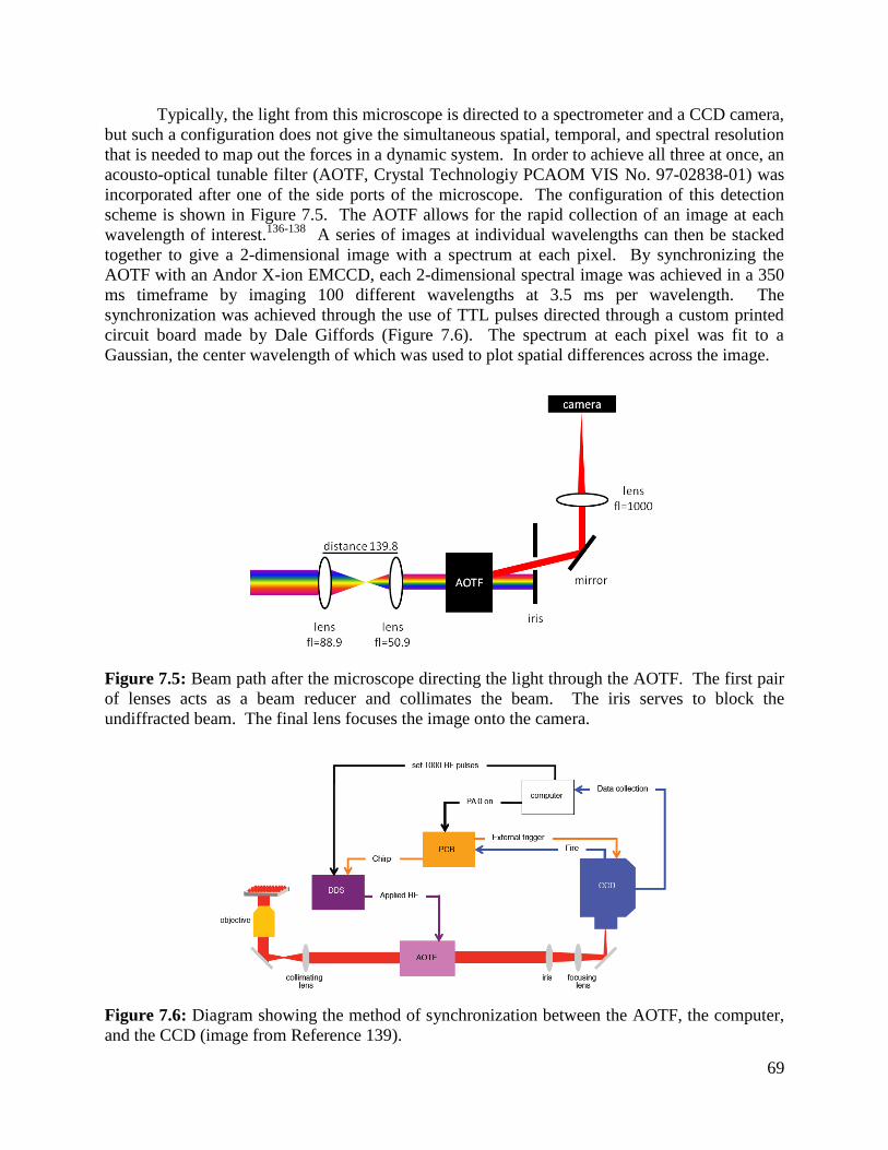
69
Typically, the light from this microscope is directed to a spectrometer and a CCD camera,
but such a configuration does not give the simultaneous spatial, temporal, and spectral resolution
that is needed to map out the forces in a dynamic system. In order to achieve all three at once, an
acousto-optical tunable filter (AOTF, Crystal Technologiy PCAOM VIS No. 97-02838-01) was
incorporated after one of the side ports of the microscope. The configuration of this detection
scheme is shown in Figure 7.5. The AOTF allows for the rapid collection of an image at each
wavelength of interest.136-138
A series of images at individual wavelengths can then be stacked
together to give a 2-dimensional image with a spectrum at each pixel. By synchronizing the
AOTF with an Andor X-ion EMCCD, each 2-dimensional spectral image was achieved in a 350
ms timeframe by imaging 100 different wavelengths at 3.5 ms per wavelength. The
synchronization was achieved through the use of TTL pulses directed through a custom printed
circuit board made by Dale Giffords (Figure 7.6). The spectrum at each pixel was fit to a
Gaussian, the center wavelength of which was used to plot spatial differences across the image.
Figure 7.5: Beam path after the microscope directing the light through the AOTF. The first pair
of lenses acts as a beam reducer and collimates the beam. The iris serves to block the
undiffracted beam. The final lens focuses the image onto the camera.
Figure 7.6: Diagram showing the method of synchronization between the AOTF, the computer,
and the CCD (image from Reference 139).

70
A detailed description of the AOTF used in these experiments, its synchronization, and
its use is provided in Appendix B of this dissertation.
7.4 Results and Discussion
A single monolayer of tetrapods was covalently linked to an amine coated glass slide.
The fluorescence from the monolayer was bright and uniform across the size of the laser beam.
While some defects in the monolayer could be observed from the fluorescence image, there were
always large areas of uniform fluorescence available for imaging. A 2-dimensional spectral
image could easily be obtained from the monolayer of tetrapods.
Figure 7.7: a.) A fluorescence image of the tetrapod monolayer showing the uniform
fluorescence of the tetrapods. The scale bar is 100 µm. b.) A schematic showing the covalent
linking of the tetrapods to the substrate. (Figure from Reference 139)
HL-1 cardiomyocytes cultured on top of these fluorescent substrates showed the
spontaneous contratractile behavior characteristic of this particular cell line (Figure 7.8).135
Because of the atmospheric environment under which these measurements were obtained, the
cells did not beat regularly as they would have in an environment with a controlled CO2
concentration.
Figure 7.8: Brightfield image of HL-1 cardiomyocytes. The black lines indicate an area of the
culture that was beating. The lines get closer together as the cells contract. The yellow color is
due to a laser line filter.
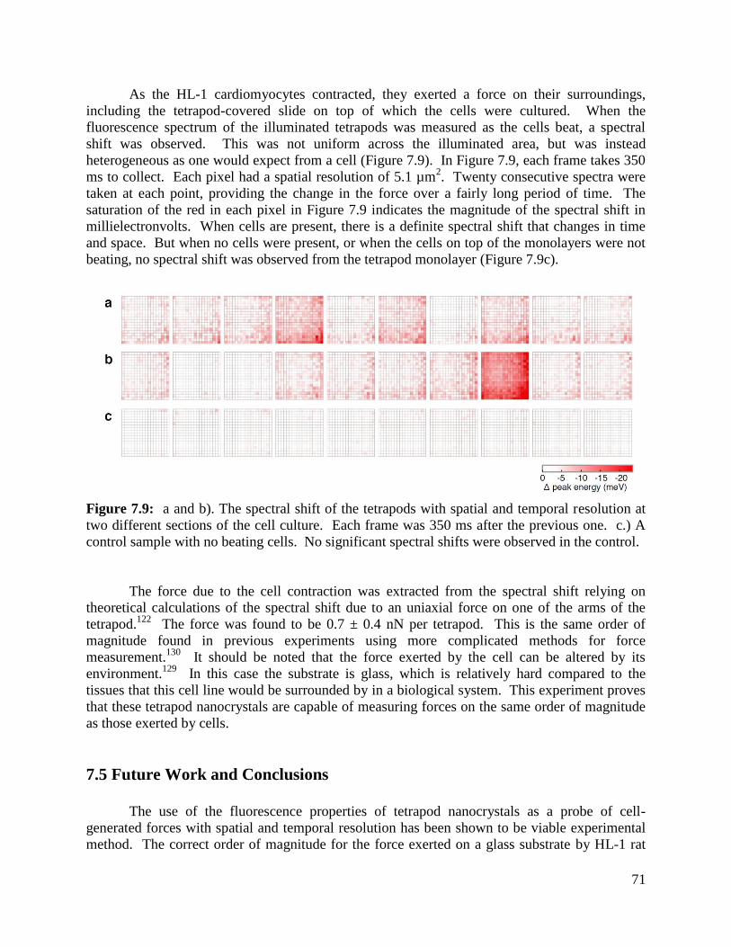
71
As the HL-1 cardiomyocytes contracted, they exerted a force on their surroundings,
including the tetrapod-covered slide on top of which the cells were cultured. When the
fluorescence spectrum of the illuminated tetrapods was measured as the cells beat, a spectral
shift was observed. This was not uniform across the illuminated area, but was instead
heterogeneous as one would expect from a cell (Figure 7.9). In Figure 7.9, each frame takes 350
ms to collect. Each pixel had a spatial resolution of 5.1 µm2. Twenty consecutive spectra were
taken at each point, providing the change in the force over a fairly long period of time. The
saturation of the red in each pixel in Figure 7.9 indicates the magnitude of the spectral shift in
millielectronvolts. When cells are present, there is a definite spectral shift that changes in time
and space. But when no cells were present, or when the cells on top of the monolayers were not
beating, no spectral shift was observed from the tetrapod monolayer (Figure 7.9c).
Figure 7.9: a and b). The spectral shift of the tetrapods with spatial and temporal resolution at
two different sections of the cell culture. Each frame was 350 ms after the previous one. c.) A
control sample with no beating cells. No significant spectral shifts were observed in the control.
The force due to the cell contraction was extracted from the spectral shift relying on
theoretical calculations of the spectral shift due to an uniaxial force on one of the arms of the
tetrapod.122
The force was found to be 0.7 ± 0.4 nN per tetrapod. This is the same order of
magnitude found in previous experiments using more complicated methods for force
measurement.130
It should be noted that the force exerted by the cell can be altered by its
environment.129
In this case the substrate is glass, which is relatively hard compared to the
tissues that this cell line would be surrounded by in a biological system. This experiment proves
that these tetrapod nanocrystals are capable of measuring forces on the same order of magnitude
as those exerted by cells.
7.5 Future Work and Conclusions
The use of the fluorescence properties of tetrapod nanocrystals as a probe of cell-
generated forces with spatial and temporal resolution has been shown to be viable experimental
method. The correct order of magnitude for the force exerted on a glass substrate by HL-1 rat

72
cardiomyocytes was determined solely by the shift in the fluorescence spectrum of the tetrapod
nanocrystals. More work is necessary to expand the systems that this technology can be applied
to.
As was previously mentioned, the force exerted on a substrate by a cell is affected by the
stiffness of the substrate that the cell is cultured on. The colloidal nature of the tetrapods allow
for the possibility of their incorporation into a variety of biologically relevant substrates,
including collagen. Collagen is a common extracellular material that is found in various forms in
the majority of animals. Bone and tendon are just two examples of tissues that consist of
collagen. Collagen consists of three amino acid chains that form a triple helix as shown in
Figure 7.10 a and b.140
The collagen molecules then form a hierarchical structure that ranges in
its size scale from nanometers to micrometers (Figure 7.10 c-e).140
In addition, the mechanical
properties of collagen are fairly well studied, making it an ideal system into which tetrapods
could be incorporated.140
Collagen has free amino groups on its molecules, allowing for the
same EDC/sulfo-NHS chemistry to be performed to covalently link the tetrapods to a collagen
substrate.
Figure 7.10: a and b). A schematic from reference 158 showing the molecular structure of a
single collagen molecule. c, d, and e). The hierarchical structure of collagen in a tendon. (image
from reference 140).
Once the tetrapods are incorporated uniformly into a collagen sample, mechanical testing
with simultaneous measurement of the fluorescence shift could be performed to acquire a better
calibration curve for the shift with force. In order to do this, a homebuilt tensile test capable of
maintaining an aqueous environment around the collagen sample, while providing a window by
which the excitation and the collection of the emitted light can still occur was built (Figure 7.11).
The stretching of the sample is performed by a small motor of the type typically used to move
around optics on a laser table. Combining the tensile test with the fluorescence measurement
will provide a calibration of the spectral shift of the tetrapods with force in a biologically
relevant system. This can be then be use as a force sensitive substrate for cell culture in the
future.

73
Figure 7.11: a.) Photograph of a homemade tensile tester. b.) A collagen sample being stretched
by the tensile tester. The window below the sample allows for laser excitation and the collection
of the emitted light.
In the future, a better understanding of the interface between the tetrapod, its substrate,
and the cell is needed to understand the intricate interplay that plays a role in response of the
tetrapod nanocrystal sensor.
74
Chapter 8
Conclusions and Future Work
8.1 Conclusions
In conclusion, this work has demonstrated that small changes to the structure of a
nanomaterial can affect the phase transition pressure. For the CdSe/ZnS core/shell system, it was
found that for shell thicknesses below the critical thickness, the upstroke phase transition
pressure is reduced. The presence of the shell changed not only the thermodynamics of the
system, but also the optical properties of the nanocrystals under high pressure. The fluorescence
peak goes from a single Gaussian in pure CdSe nanocrystals to multiple peaks for the core/shell
system under high pressure. From this, it can be hypothesized that in the case of the CdSe/ZnS
core/shell system, a material combination with smaller lattice mismatch would yield a smaller
change initially, but a better trend could be developed, as the critical thickness would be much
greater. In the case of Bi2Se3 intercalated with copper, the phase transition pressure was
increased relative to the same nanoribbons with no copper. These systems provide a unique
insight into the interplay of material strain and thermodynamics through the manipulation of the
phase transition conditions.
Furthermore, a better idea of the mechanism of the phase transition in cadmium sulfide
nanocrystals has been elucidated from ultrafast shock wave experiments performed with an X-
ray probe. The h-MgO intermediate was observed for the first time, in accordance with its
prediction from theory.100-103
Because the h-MgO intermediate was found only at low shock
stress and it was never the majority phase, it was determined that multiple transformation
pathways are followed.
The possibility of performing single nanoparticle optical experiments under high pressure
was also explored. While steps were taken towards correcting the spherical aberration, no one
method proved sufficient to correct the aberration in a functional manner. Additional problems
with the sample and sample loading were revealed.
In addition, the optical properties of tetrapod nanocrystals under pressure were used to
observe and quantify the force exerted by a HL-1 cardiomyocytes. While not the first time such
a force has been quantified, tetrapod nanocrystals provide a sensor that allows for data collection

75
with both spatial and temporal resolution. An AOTF on the detection side of a fluorescence
microscope allowed for the collection of the data with spatial, temporal, and spectral resolution.
This technique also allows for the future quantification of forces in biology on the size scale that
they are actually exerted (the nanoscale). This technique can be extended to biologically
relevant systems, such as collagen.
There are many outstanding questions with regards to phase transitions in nanocrystals.
While steps towards addressing some of them have been addressed in this work, more
experiments are needed.
8.2 Future Work
8.2.1 Introduction
There remains a large body of work that has yet to be performed regarding phase
transitions in nanocrystals. This section is meant to provide a brief overview of several
outstanding questions in the fields of high pressure and high temperature structural phase
transitions and melting phenomena in nanocrystals and the experiments that would provide some
insight into these important questions.
8.2.2 High Pressure Behavior of Doped Nanocrystals
It is well known that phase transitions in bulk crystals nucleate at defects in the lattice.
2
Crystal defects include grain boundaries, twin boundaries, substitutional defects, and interstitial
defects. An example of a substitutional defect is shown in Figure 8.1. An interstitial defect sits
between lattice points instead of replacing one of the atoms. In a perfect crystal, even the surface
can be considered a defect, as the atomic/molecular environment at the surface is different than
the bulk of the crystal. A defect can introduce a site in the crystal where the energy barrier that
must be overcome to nucleate the new phase is less than in the perfect lattice, thus nucleation of
the new phase at a defect site is preferred.37
The effect of these defects on the phase transition in
nanocrystals is unknown.
Doped semiconductor nanocrystals can now be synthesized with a number of different
dopants141-146
and would provide an ideal case study for investigating the effect of substitutional
and interstitial defects on the phase transitions. For substitutional dopants, the dopant is never
the same as size as the cation or anion that is supposed to occupy that position in the lattice; they
will be either larger or smaller. This will cause a strain field to be present around the dopant.
Dopants located in the interstitial sites will also induce a strain field around the impurity, as they
occupy a site that is not typically populated and the surrounding atoms must change their
positions to accommodate this. There are several examples of synthetic routes that yield Mn2+
and Cu2+
doped CdSe nanocrystals with the dopant in the bulk of the crystal instead of on the
surface.141,145
One paper even cites the ability to controllably synthesize CdSe nanocrystals with
exactly four copper atoms per particle.141
This is an important advance in synthetic techniques,
as nanocrystals are naturally self purifying and usually impurities are pushed to the surface

76
during growth.36
Other dopants in CdSe nanocrystals include Ag2+
, Mg2+
, and Co2+
, but the
lattice position of the dopant in these systems is not as well characterized.143,144,146
Figure 8.1: An example of a substitutional defect. The red atom represents the defect. In this
case, the atoms around the defect move to accommodate the smaller size of the defect.
In nanocrystals, the effect of defects (besides the surface) on the high pressure phase
transition behavior has yet to be investigated. In doped nanocrystals, the dopant site and
surrounding strain field introduces a defect into the once "perfect" nanocrystal. Given that the
high pressure phase transition in bulk crystals nucleates at the defect sites present in the crystal,
it follows that the dopant sites should provide lower energy nucleation sites in the nanocrystal.
While this would probably have a minimal effect on the thermodynamics of the system, the
kinetics of the system should be affected to a greater extent. For instance, the increased width of
the hysteresis curves for CdSe nanocrystals relative to the bulk has been attributed to the lack of
nucleation sites. If nucleation sites are introduced in the nanocrystal through doping, then the
overpressurization needed to induce the nucleation and growth of the new phase should decrease
due to a lowered activation energy. A similar process should be in effect for the pressure
downstroke, where the underpressing necessary to induce the reverse transition should be less.
This would yield a narrowing of the hysteresis curve when dopants are present.
Since recent synthetic procedures have shown the ability to dope CdSe nanocrystals with
different ions,141,143-146
it can be imagined that the effect of the dopant on the phase transition
could be tuned by changing from one dopant to another. A greater change in the phase transition
conditions could be observed when there exists a larger difference in the size or oxidation state
between the dopant ion and those in the host lattice.
In addition, it is easily imagined that the number of dopants per nanocrystal could also
play a role in the high pressure phase transition behavior. More dopants would yield more

77
available nucleation sites. This could yield faster transformations and the possibility for multiple
nucleation steps per particle. Multiple nucleations in a single particle would yield fractured or
multi-domain particles.
Given the possibility that dopants change the phase transition such that the upstroke
phase transition is reduced for nanoparticle, a more accessible method for the synthesis of the
high pressure structural phases of semiconductor nanocrystals could be achieved.
8.2.3 Cobalt Phase Transitions at High Temperature
Nanoparticles of cobalt have been found to exist in a phase that had not been previously
found in bulk.147
Bulk cobalt can be found as two different structures: face-centered cubic (fcc)
and hexagonal close-packed (hcp). The fcc phase is preferred at higher temperatures, while a
mixture of hcp and fcc can be found under ambient conditions.147
The two structures differ only
by their stacking along the 111 direction (hcp exhibits ABAB stacking, while fcc exhibits
ABCABC stacking). Stacking faults are thus common in crystals of cobalt because the energy
between the two structures is low.147
For nanoscale cobalt, an additional crystal structure was
discovered: ε-cobalt (ε-Co).147
The unit cell of ε-Co is cubic with a=6.097 Å and is similar to
that of β-manganese with Z=20.147
Nanoparticles are easily synthesized in the hcp phase and the
ε-Co phase (Figure 8.2).148-150
It has been found that the hcp nanoparticles of Co transform to the
ε-Co phase when heated to about 200 °C.148
The ε-Co then transforms to fcc when heated about
around 500 °C.148
Figure 8.2: Transmission electron micrographs of spherical ε-Co nanoparticles synthesized
through the decomposition of Co2(CO)8.
These phase transitions have not been well characterized. Simple differential scanning
caloritmetry (DSC) would provide an idea of the relative energies of the structures. Preliminary
experiments (taken by Simone Raoux at Brookhaven National Lab on particles synthesized in the
Alivisatos group by Mark Polking and the author) using temperature dependent X-ray diffraction
confirm the phase transition from ε-Co to the fcc structure (Figure 8.3). It also seems to indicate
a low scattering, or amorphous phase at higher temperatures. During experiments such as this,
extreme care must be taken in order to avoid coalescence and sintering of the nanoparticles. This
yields larger particles that will lead to a biasing of the size dependent results.

78
Figure 8.3: a.) XRD pattern of 6.9 nm diameter ε-Co nanoparticles before heating. b.) The
temperature ramp profile for the experiment. c.) XRD pattern for the recovered fcc phase of Co.
d.) The diffraction pattern of the Co nanoparticles with time during the temperature ramp in b.
It is conceivable that single particle experiments investigating the phase transition in Co
nanoparticles could be achieved with an ultra-stable heating stage in an electron microscope (see
below).
8.2.4 Single Particle Phase Transition Behavior
While Chapter 6 of this dissertation outlines some of the steps that have been taken
towards optically probing the high pressure phase transition in semiconductor nanocrystals at the
single particle level, more must be done in order to understand the behavior of single
nanoparticles as they undergo a structural phase transition. This applies not only to phase
transitions that occur under pressure, but also those that occur with temperature. Examples of
nanocrystal systems with structural phase transitions that take place with changes in temperature
include cobalt,148
germanium telluride,151
and copper sulfide.152
Cobalt nanocrystals will
transform from its ε-Co structure (unique in that this phase is only seen in nanocrystals) to a face
centered cubic modification with increased temperature.148
Germanium telluride shows a size
dependent phase transition with temperature from a rhombohedral structure (R3m) to a rocksalt
temperature.151
The low chalcocite to high chalcocite phase transition in copper sulfide
nanoparticles is size dependent and can be induced by an electron beam in a transmission
electron microscope.152-153
Experimentally, it is much easier to change the temperature of a sample than to apply the
type of pressures that are needed for the observation of the phase transitions previously
discussed. The most straightforward method to observe single particles and molecules that is
commonly used is to observe their fluorescence. Unlike the II-VI semiconductor nanocrystals
discussed in Chapter 6, the samples mentioned above are not photoluminescent, thus

79
fluorescence cannot be used in these cases. With the advent of ultra-stable transmission electron
microscope holders capable of heating the sample in a controlled manner while maintaining good
image resolution and stability, electron microscopy seems to be uniquely positioned to offer the
structural characterization needed for high temperature phase transitions on a nanoparticle by
nanoparticle basis. Studies of this sort could investigate the size, shape, and faceting dependence
of the structural phase transitions. High resolution electron microscopy would offer insights into
the phase transition mechanism, while ultrafast electron microscopy techniques would provide
the necessary kinetics data. The downside of electron microscopy is that the electron beam itself
has the ability to do chemistry and thus must be accounted for in each and every experiment.
Also, electron microscopy techniques are not as high throughput as single particle fluorescence
imaging.
In addition to electron micrscopy techniques, there are several beamlines at synchrotron
sources that have managed to achieve an extremely small beam size. If the sample being
observed possessed a high scattering coefficient and the beam size was made small enough such
that only one particle was exposed to the beam at as time, then the observation of diffraction
from a single particle should theoretically be observable. Unfortunately, given the limits of
current detectors, the exposure time for a diffraction pattern of from an individual nanoparticle
may be extremely long. This would only allow for steady state measurements without the
possibility of observing any short lived intermediate states. Free electron lasers, such as the
LCLS at SLAC, may be able to achieve the necessary beam intensity in a short period of time to
allow for the structural characterization of a single nanocrystals while still allowing for temporal
resolution.
8.2.5 Ultrafast Measurements of Laser Induced Nanocrystal Melting
When a semiconductor is heated, eventually the material undergoes a solid to liquid
phase transition at its melting point. This process occurs in a similar method to the solid-solid
phase transitions discussed earlier; the nucleation of the liquid phase inside the solid occurs at
defects in the crystal including the surface of the crystal.154
Under normal heating conditions the
rate of change of the material from a solid to a liquid depends on the extent of superheating and
is limited by the speed of sound in the crystal.155
When laser irradiation is used to heat the
sample, nonthermal melting becomes possible at high laser fluences.154-156
Nonthermal melting
results from the generation of a large number of electron-hole pairs, which create an extremely
dense e-h plasma.154
This makes the lattice unstable and it begins to lose its crystallinity, thus
starting the melting process. It relies on the transfer of the absorbed energy from the laser to
phonon modes.154
Nonthermal melting takes place on a time scale much faster than that
observed for thermal melting (~100 ps) because the energy transfer to the phonons is extremely
fast (~200 fs).18
In semiconductor nanocrystals, the melting point is highly size dependent.149
In addition,
nanocrystals are also expected to have a phonon bottleneck, where the number of phonons that
can be supported by a single nanocrystal is limited.157-158
This could yield very different melting
phenomena when the crystals are subjected to high laser fluences. Nanocrystals have a high
surface to volume ratio which will also play a role in the melting process. Preliminary
experiments performed at the LCLS at SLAC, provide X-ray diffraction patterns of cadmium

80
sulfide nanocrystals at picosecond time delays after exposure to various laser fluences (Figure
8.4). The diffraction from nanocrystals is usually weak, thus in order for a thin enough sample to
be investigated without heat transfer concerns, a high intensity, pulsed X-ray source, such as the
LCLS was necessary. From experiments such as these, the facet dependence of melting and the
size dependence could be extracted from the diffraction data. It is also possible that a size
dependence of the transition from thermal to nonthermal melting could be observed.
Figure 8.4: X-ray diffraction patterns of a 4.4 nm by 18.4 nm CdS nanorod sample at different
time delays after being irradiated with a 540 µJ pulse. The blue trace in each plot is a scan of the
sample before irradiation, while the red is a scan at the given time delay.

81
Appendix A
Diamond Anvil Cell Basics
A.1 Introduction
In general, a diamond anvil cell consists of two metal plates opposing each one another.
A diamond is placed on each plate in a geometry such that as the metal plates are brought closer
and closer together, the diamonds exert more and more pressure on the sample between them.
Given that a sample needs to be placed between the diamonds, the diamonds are specially cut to
possess a flat culet instead of the pointed culet that is typically used in jewelry (Figure A.1).
Other diamond geometries are used in addition to the brilliant cut shown in Figure A.1, but were
not used in the course of this work.
Figure A.1: An example of the diamonds used in a diamond anvil cell.
Typically, the sample is contained within a pre-indented and drilled gasket that this held
between the two diamonds. Included with the sample are a pressure gauge (such as ruby) and a
pressure transmitted medium (Figure A.2). The preparation of the gasket and the loading of the
sample will be discussed later.
Before use, the diamonds in the diamond anvil cell (DAC) must be aligned relative to
each other to avoid the fracture and chipping of the diamonds. Care must be taken during this
process so that the diamonds never touch one another, which will cause damage. The process for
alignment varies for each DAC type. Three different, but similar methods, are discussed here for
different cell types.
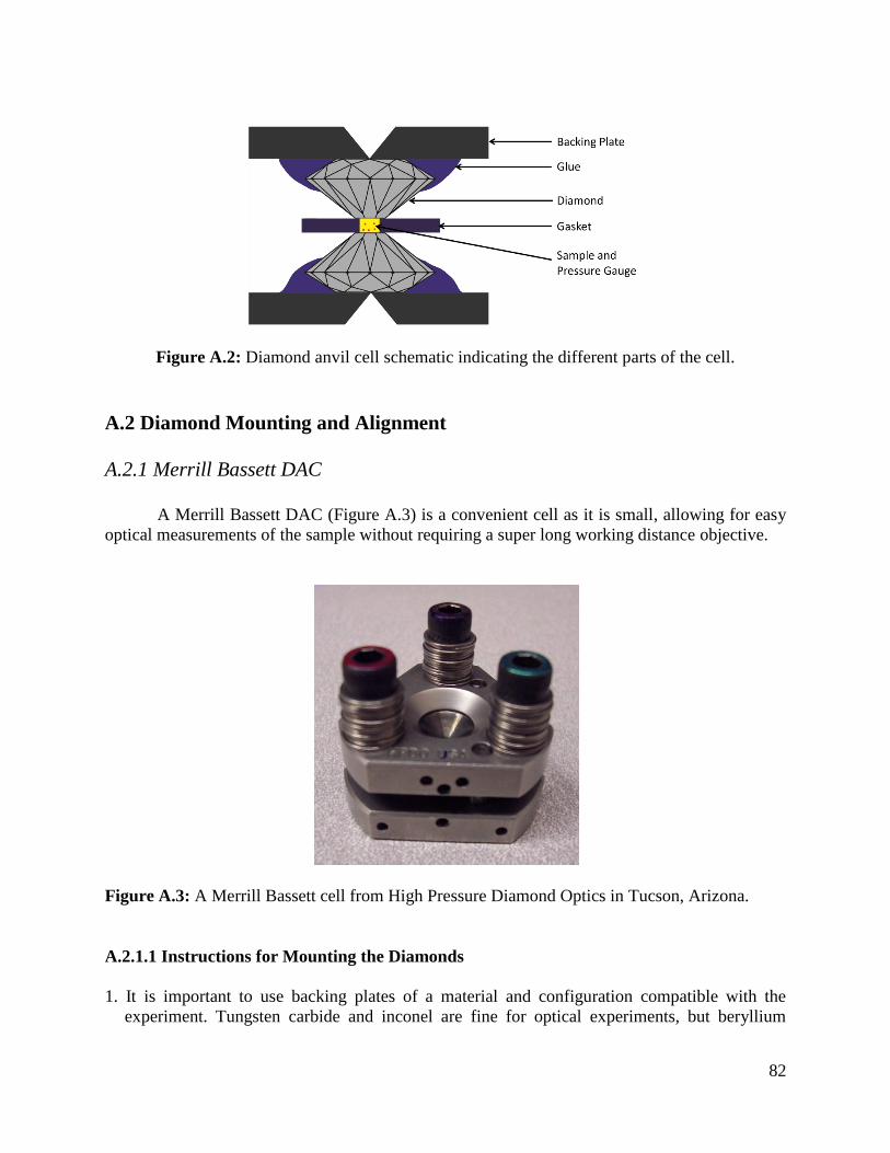
82
Figure A.2: Diamond anvil cell schematic indicating the different parts of the cell.
A.2 Diamond Mounting and Alignment
A.2.1 Merrill Bassett DAC
A Merrill Bassett DAC (Figure A.3) is a convenient cell as it is small, allowing for easy
optical measurements of the sample without requiring a super long working distance objective.
Figure A.3: A Merrill Bassett cell from High Pressure Diamond Optics in Tucson, Arizona.
A.2.1.1 Instructions for Mounting the Diamonds
1. It is important to use backing plates of a material and configuration compatible with the
experiment. Tungsten carbide and inconel are fine for optical experiments, but beryllium

83
should be used for X-ray experiments. The available collection angle can also be changed as
deemed appropriate for the experiment being performed.
2. The selected backing plate is placed in a diamond jig. A diamond jig consists of a base with 3
set screws to hold the backing plate in place and a vertical screw or column with a hole drilled
through the middle for visualization of the diamond. The diamond is then placed on top of the
backing plate and held in place by the vertical screw. A stereoscope can then be used to align
the diamond culet over the center of the backing plate hole by adjusting the position of the
backing plate relative to the diamond through the use of the set screws. Once centered, the
vertical screw is secured so that the diamond and backing plate cannot move.
3. The diamond is now ready to be glued down. For most applications Stycast 2850 FT with
Catalyst 23LV is an appropriate adhesive. It is fairly impervious to the solvents used in the
work presented here. If heating is required, a different adhesive may be more appropriate.
After mixing the resin and the catalyst, the glue can easily be applied by using a syringe
needle or a small broken drill bit. It is important that the glue is not applied too close to the
culet or allowed to touch the screw holding the diamond in place. This can cause problems
later when removing the backing plate and diamond from the jig.
4. Once the glue is dry (24 hours for Stycast), the backing plate with the attached diamond can be
removed from the diamond jig. It can then be secured in the Merrill-Bassett cell through the
use of the three set screws present on each half of the cell. The backing plate should be held
flat against the cell and not at an angle, in order for the diamonds to be parallel to each other.
A.2.1.2 Instructions for Aligning the Diamonds
1. Before assembling the two halves of the cell, cover one of the untapped screw holes with a
piece of metal (this can be leftover gasket if the metal piece is large enough to cover the hole)
held in place with a piece of molding clay on the same side of the cell as the diamond. It is
important to clean the culet surfaces with cotton swabs and solvent to make sure no dust,
excess glue, or other particulates are present. Then align the red dots on the side of the cell,
and carefully push the two sides together without letting the two diamonds touch.
2. The cell can then be turned upside down such that the tapped screw holes are on top. Using
the tapped hole above the covered hole on the bottom, thread a screw through the hole until it
is touching the metal piece. By adjusting this screw, the distance between the diamonds can
be changed accordingly. The diamonds should initially be at least a culet width apart.
3. By using the set screws on half of the cell that is now on the bottom, the position of the bottom
diamond can be adjusted so that it sits directly below the top diamond. It is not recommended
that the top diamond be adjusted, as loosening the set screws can cause the backing plate to
become unseated and susceptible to gravity. Not only should the bottom diamond be directly
below the top diamond, but the facets should be aligned to the best of the user's ability. Not
all diamonds are perfectly cut, so the user's judgment is generally required as to the when the
diamonds are aligned.

84
4. A Merrill-Bassett cell does not possess any tilt alignment for the diamonds. As long as the
cell and the backing plates are machined to a high degree of tolerance in terms of flatness, the
tilt alignment does not usually pose a problem. It can be checked by carefully by placing the
two diamonds in contact with each other and counting the number of rainbows visible across
the cell. The fewer colors present the better the parallelism.
A.2.2 Diacell Piston Cylinder DAC
The Diacell piston cylinder DAC is unique in that it can be pressurized through two
methods: through the use of screws or through the use of an inflatable bellow. The bellow
pushes down on the cylinder as it is inflated, thus generating the pressure.
Figure A.4: Diacell piston cylinder DAC.
A.2.2.1 Instructions for Mounting the Diamonds
1. It is important to once again choose the appropriate backing plates for the experiment that is to
be performed. In addition, the diamonds chosen should have metal rings fitted to them of an
appropriate metal such that it does not interfere with the characterization method chosen.
2. To mount the diamonds, carefully unscrew the metal pieces that hold the diamonds and
backing plates in place. Then, simply place the metal-ringed diamonds on top of the backing
plate and replace the metal pieces to hold the diamonds in place. No glue is necessary for this
type of diamond anvil cell.
A.2.2.2. Instructions for Aligning the Diamonds
1. The alignment procedure is similar to the method to that used for a Merrill Bassett cell. The
main exception is that there is enough friction between the two cell halves that there is no
need to use a screw to hold the diamonds apart.
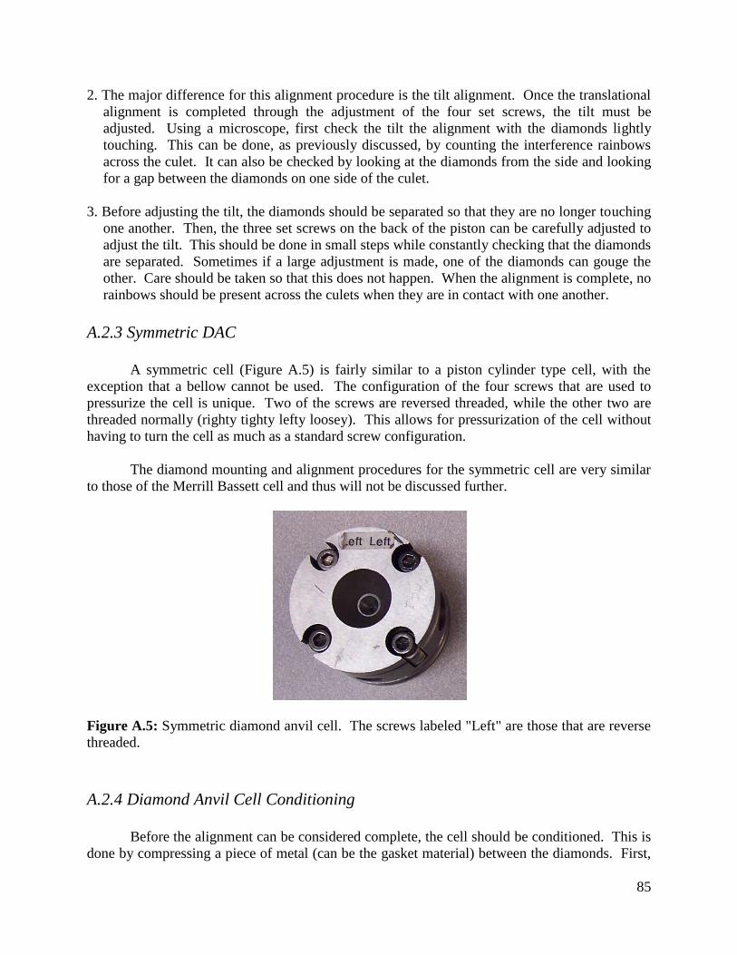
85
2. The major difference for this alignment procedure is the tilt alignment. Once the translational
alignment is completed through the adjustment of the four set screws, the tilt must be
adjusted. Using a microscope, first check the tilt the alignment with the diamonds lightly
touching. This can be done, as previously discussed, by counting the interference rainbows
across the culet. It can also be checked by looking at the diamonds from the side and looking
for a gap between the diamonds on one side of the culet.
3. Before adjusting the tilt, the diamonds should be separated so that they are no longer touching
one another. Then, the three set screws on the back of the piston can be carefully adjusted to
adjust the tilt. This should be done in small steps while constantly checking that the diamonds
are separated. Sometimes if a large adjustment is made, one of the diamonds can gouge the
other. Care should be taken so that this does not happen. When the alignment is complete, no
rainbows should be present across the culets when they are in contact with one another.
A.2.3 Symmetric DAC
A symmetric cell (Figure A.5) is fairly similar to a piston cylinder type cell, with the
exception that a bellow cannot be used. The configuration of the four screws that are used to
pressurize the cell is unique. Two of the screws are reversed threaded, while the other two are
threaded normally (righty tighty lefty loosey). This allows for pressurization of the cell without
having to turn the cell as much as a standard screw configuration.
The diamond mounting and alignment procedures for the symmetric cell are very similar
to those of the Merrill Bassett cell and thus will not be discussed further.
Figure A.5: Symmetric diamond anvil cell. The screws labeled "Left" are those that are reverse
threaded.
A.2.4 Diamond Anvil Cell Conditioning
Before the alignment can be considered complete, the cell should be conditioned. This is
done by compressing a piece of metal (can be the gasket material) between the diamonds. First,

86
compress the metal only slightly. Then, disassemble the cell and check the diamond alignment.
Then, repeat with progressively higher pressures until the diamonds no longer need to be
adjusted. If there is a large change in the alignment, start over from low pressures.
A.3 Gaskets
A gasket between the diamonds serves as a sample chamber and an easy method for
keeping the diamonds from coming into contact with one another. The gasket plays a crucial
role in what pressures are achievable by the DAC.28-29
It can also determine what geometry the
sample can be observed from. In an axial geometry (probing and collecting through the
diamonds) metal gaskets, such as stainless steel, spring steel, and rhenium are typically used.
Typically, the harder metals are used for experiments that reach higher pressures. In a radial
geometry (probing and collecting between the diamonds), beryllium and boron epoxy gaskets
can be used.43
Because of its toxicity, the use of beryllium is usually avoided. A gasket also
supports the sample material under pressure, which increases the maximum pressure that is
achievable.28-29
A gasket is usually pre-indented before drilling. This prevents the flow of metal from
filling in the hole as the pressure is increased and helps the mechanical stability of the gasket.28-29
A.3.1 Instructions for Gasket Indentation
1. It is important to choose the gasket material most appropriate for the pressures that are to be
achieved in the experiment. This should be cut into small enough pieces such that they easily
fit into the cell. It should be recalled that these will sometimes have sharp edges so
appropriate care should be taken.
2. To save time later, it is important to carefully measure the distance from the table of one
diamond to the table of the other. This is easily achieved through the use of a micrometer
with probes small enough to rest within the aperture of the backing plate while the diamonds
are in contact with one another.
3. The gasket metal and the diamonds should be cleaned with solvent and a cotton swab to make
sure that they are free of dirt and fibers before the gasket metal is secured in place over one of
the diamonds using a small piece of molding clay on the edge. A mark should be scratched
into the surface of the gasket with a diamond tipped pen pointing to some reference point on
the cell so that the gasket can be replaced later in the same position.
4. The cell can then be assembled with the gasket metal between the diamonds. Pressure can
then be carefully exerted on the metal by carefully and slowly turning the DAC screws. Care
should be taken to make sure the screws are replaced in the same positions from which they
were removed every time the cell is used. The best method to go up slowly in a controlled
fashion is to turn each screw about one sixth of a full turn (Figure A.6). It is sometimes
helpful, especially when learning, to draw out this diagram to help with the consistency of
each turn.

87
5. In order to check the thickness of the gasket as it is being indented, the distance between the
tables of the diamonds can be periodically measured. When a distance between the tables
without the gasket (Step 2) plus 70-90 µm is achieved, then the gasket between the diamonds
is thin enough.
Figure A.6: Diagram showing a single turn. This picture is helpful when pressurizing the DAC
using the screws.
6. The pressure can then be released slowly. It is important to use the same one sixth turns
defined in Figure A.6 and to reverse the order in which the screws are turned. If you
tightened the screws in a clockwise direction around the circumference of the cell, then loosen
the screws in a counterclockwise order.
7. The final thickness of the indent can then be measured using a micrometer with thin points.
A.3.2 Gasket Drilling
Once pre-indented, the gasket can then be drilled. There are several methods available in
order to drill a small enough hole. As a generally excepted rule, the hole should be about one
third to one half of the culet size.28
This can be achieved through a mechanical drill, spark
erosion, or a laser miller. A laser miller gives the best shaped hole that is free of metal burrs.
All of these methods were used in the work presented here.
A.4 Samples and Loading
A.4.1 Pressure Gauges
There are several pressure gauges that can be used within the DAC. One of the most
commonly used manometers is the fluorescence of ruby (Cr3+
doped Al2O3). The fluorescence
of the R1 and R2 lines are been thoroughly characterized and found to shift 0.365 nm/GPa.44
The
splitting and broadening of these peaks can also be used to help determine the nature of the
88
pressure within the cell (hydrostatic or nonhydrostatic).44
Other optical sensors include Sm2+
doped SrB4O7, BaFCl, and SrFCl and Eu3+
doped LaOCl and Y3Al5O12.28
These have a range of
sensitivities and can in some cases also be used to determine temperature. Some of the common
non-optical pressure calibrants are those that are diffraction standards. These include NaCl,
CaF2 (fluorite), SiO2 (quartz), CsCl, Al, Au, Pd, Pt, and Ag.28,44
A.4.2 Pressure Transmitting Medium
The medium that surrounds the sample in the gasket chamber is extremely important.
The medium can be a gas, solid, or a liquid. The easiest to load are pressure transmitting media
that are liquids under ambient conditions. An important consideration when choosing a pressure
transmitting medium is whether or not it has been shown to exert hydrostatic pressure on the
sample in the chamber. In addition, for nanoparticles, it is important that the particles are soluble
in the medium for ease of loading and in order to avoid coupling between particles. A more
complete list of pressure transmitting media can be found elsewhere,1 but those relevant to the
studies shown here are ethylcyclohexane and a 1:1 mixture of pentane: isopentane.
A.4.3 Sample Loading and DAC Use
There are several methods by which a sample can be loaded, differing mostly by sample
type and personal preference. The method described below seems to work fairly well for loading
nanoparticles into the diamond anvil cell.
1. The easiest way to prepare the sample is to dry off the solvent that the nanoparticles are
dissolved in and then re-dissolve it in the chosen pressure transmitting medium.
2. Before beginning, the diamonds must be clean and free of any fibers and dirt. It is important
to secure the drilled gasket on top of the bottom diamond. This can be done by aligning the
mark on the gasket to the reference point on the DAC body and gently pushing down so that
the gasket locks into place on the culet. It is helpful to make sure that the gasket surface is
clean in addition to the diamonds so that the gasket does not get the culet dirty while it is
being secured. A small piece of molding clay can be used to hold the gasket in place.
3. Using an acupuncture needle or similarly thin probe, a small amount of ruby (or a thin piece of
gold) can be carefully transferred to the inside of the gasket hole. It is important that this is
not thicker than the gasket. Bridging the diamonds can cause errors in the pressure
measurement and sometimes damage to the diamonds.
4. The sample can then be added to the gasket hole. Very carefully using a syringe, a single drop
of the sample in the pressure transmitting medium can be added on top of the gasket hole. If
the concentration of the sample is not high enough another drop can be added, or in the case
of a single component pressure transmitting medium, the sample can be allowed to
concentrate before closing the cell. This cannot be done with multi-component pressure
transmitting media, as the components will evaporate at different rates.

89
5. The DAC can then be closed and sealed by turning the screws several times. The number of
turns (defined in Figure A.6) necessary to seal the cell depends greatly on the DAC being used
and the gasket material. A microscope can then be used to check for air bubbles in the gasket
hole. Sometimes air bubbles can be gotten rid of by further pressuring the cell, but the
majority of the time the cell needs to be reloaded.
6. The pressure can then be increased between measurements by turning the screws by the one-
sixth turn described above. At low pressures several one-sixth turns may be necessary to
increase the pressure, while at higher pressures less than one-sixth of a turn may be used.
Consistently turning all of the screws to the same extent is necessary in order to maintain a
hydrostatic environment and prevent a large pressure gradient across the culet.

90
Appendix B
AOTF Synchronization and Use
B.1 Introduction
The acousto-optic tunable filter, or AOTF, is a useful tool in optics for dynamically
controlling the wavelength of light allowed through the filter. It can be placed before a
fluorescence microscope to serve as an excitation filter or on the detection side of the microscope
to provide spatial, temporal, and spectral resolution.18-20
It works through the use of a
birefringent crystal and an applied radio frequency. The applied radio frequency sets up a type
of grating across the crystal which diffracts a single wavelength of light at a different angle from
the remaining wavelengths (Figure B.1). The two polarizations of the selected wavelength end
up on opposite sides of the undiffracted beam.18
As the radio frequency is changed, the
diffracted wavelength changes. The image is maintained throughout this process, allowing for
spatial resolution to be acquired. When the AOTF is placed on the detection side of a
fluorescence microscope setup, one can collect an image at a series of wavelengths and combine
the images such that each pixel of the resulting image has a spectrum associated with it,
providing spectral resolution.19
Because changing the radio frequency quickly can be achieved
with relative ease, temporal resolution can also be obtained, being only limited by the collection
times of the camera.
Figure B.1: Diagram of the input and output of an AOTF when a radio frequency is applied
across the crystal.

91
B.2 Instrument and Synchronization
Many AOTF's only accept collimated light; off axis light is rejected by the instrument.
As such, the light directed out of the microscope must be recollimated and shrunk in order to
pass through the AOTF input aperture. Our Zeiss Axiovert microscope require the use of 2
doublet lenses of focal lengths 88.9 mm and 50.9 mm to collimate and reduce the output light
size. These lenses were configured as shown in the Figure B.2. It is important to note that the
lenses must be adjusted for the wavelength range to be used. For example, if the red light is to
be collected, the lenses should be aligned such that red light is collimated. The chromatic
aberration introduced by the lenses is significant enough that when the lenses are aligned to
collimate red light, blue light will not be collimated.
Once the light passes through the AOTF, a convenient method to block the undiffracted
beam is through the use of an iris or diaphragm (Figure B.2). The diffracted beam can simply be
directed through the aperture of the iris and then focused onto the camera using an additional
doublet lens.
Figure B.2: The beam path after the microscope directing the light through the AOTF. The first
pair of lenses act as a beam reducer and collimates the beam. The iris serves to block the
undiffracted beam. The final lens focuses the image onto the camera.
In order for the AOTF to be used for spatially and temporally resolved spectroscopy in a
meaningful way, it must be synchronized with the camera. In our experiments, an AOTF from
Crystal Technology (PCAOM VIS No. 97-02838-01) with a DDS controller (Crystal Technology
No. 20160) was used in combination with an Andor iXon 897 EMCCD. The synchronization of

92
these two instruments was achieved through the use of a National Instruments data acquisition
(DAQ) PCI card (NI PCI-6503 NI-DAC MX) and a custom printed circuit board made by Dale
Giffords. The DAQ was connected to the printed circuit board through the use of a ribbon cable
(see Figure B.3). The printed circuit board was then connected to the DDS AOTF controller
through the use of another ribbon cable. In order for the AOTF controller and the camera to
communicate, two additional connections were made from the printed circuit board to the Andor
camera. These cables, which have a BNC connection on one end and a special interface specific
to Andor cameras on the other, connected the printed circuit board to the external trigger and fire
port of the camera (Figure B.3). With these connections, the AOTF and the camera can
communicate with one another.
Figure B.3: Connections between the AOTF controller, the Andor iXon, and the computer
(through the DAQ). The instruments must be connected in this manner in order to communicate
with each other
In order to optimize the AOTF, the graphical user interface for the instrument was used to
change the frequency and the intensity of the diffracted beam after the AOTF was monitored
using the video mode of the camera. The angle and position of the AOTF was adjusted until the
highest intensity on the camera was achieved. Once the maximum intensity was achieved, the
setup was programmed to collect spectra.
The AOTF has 1024 memory slots that can be used to program different frequencies.
The amount of time that each frequency in each slot is delivered to the AOTF crystal can be
adjusted by changing the rate of the instrument. Each increment of the rate corresponds to 4
cycles of the controller's internal clock, making the rate increment 10 ns. It was found that a rate
of 34928 corresponds to about 35 µs for each programmed frequency. By programming 10 slots
with a single frequency, the time at a single frequency was 3.5 ms, which is within the temporal
restraints of the Andor camera.

93
Before a spectrum can be obtained, a program filling the desired number of memory slots
with the desired frequencies had to be generated. The AOTF controller has its own coding
language that must be used. The programs typically used for our experiments first defined the
number of memory slots to be filled and then programed the rate discussed above. Following
these two lines were the commands that defined the frequency in each slot. An example is
shown below:
chirp alloc -p0 0 1000
chirp rate -p0 0 34928
chirp freq -p0 0 0 75.20
The first part of each line tells the AOTF controller what to do: allocate memory, define the rate,
or fill in the frequency. The second part of the line, -p0, tells the controller to use Profile 0. The
numerical value following this, is the channel number. The AOTF controller used is only
capable of using a single channel, making this number was always zero. The "chirp freq"
command has an additional numerical entry which can possess values from 0 to 1023. This is
the slot number. Each slot to be filled needs its own line of code. The last part of each line is the
actual input value for that command. The code can be saved a MS-DOS text file and imported to
the controller using the command line.
In addition to the AOTF GUI, communication with the AOTF controller can also be
established through the use of a command line style interface called AOTF Cmd Interactive.
This program allows the user to program the controller using code such as that listed above and
query the instrument as to its current state. A list of common commands and queries is given in
Table B.1.
Table B.1. Useful AOTF Cmd Interactive Commands and Queries
Command Purpose
chirp mode -m 0 4 puts the controller in the correct mode
mod ana -m 0 sets the instrument up to receive signal from
the printed circuit board
dds a 0 0 sets the radio frequency amplitude to 0
dds a 0 14000 sets the radio frequency amplitude to 14000
dds a 0 asks what the radio frequency is
dds f 0 asks what the frequency in the first slot of
memory is
chirp alloc -p0 0 asks how many memory slots are used
chirp mode -p0 0 asks what mode is programmed
Once the program had been written, several pieces of software had to be used to collect
each spectral series. The Andor Solis software, LabView, AOTF Cmd Interactive, and the
computer's command line each had to be used in turn. It is useful to note that the AOTF Cmd
Interactive software cannot be used to control the AOTF if the command line is already open and
controlling the AOTF.

94
Once the AOTF had been properly aligned and optimized the following instructions were
followed in order to collect a spectral series.
B.3 Instructions for Use
1. Open the Andor Solis program and wait for the camera to cool down. Use the following as the
acquisition settings:
Acquisition mode: Kinetic
Triggering: External Start
Readout Mode: Image
Exposure Time: 0.00260 s
Number of Accumulations: 1
Kinetic Series Length: Number of images needed
Kinetic Cycle Time: 0.00350 s
Shift Speed: 1.7
Gain: 5×
EM: 300
Chip Size: 64 × 64
Binning: 2 × 2
Frame Transfer: On
Background Corrected Mode
2. Make sure that the AOTF GUI is closed.
3. In the command line of the computer, load the program defining the rate and frequencies to be
used in the experiment.
aotfcmd -t 100 -f filename.txt
It is important to wait for the program to load completely before closing the window.
4. On the desktop open "AOTF Cmd (Interactive)." To make sure that the AOTF is in the correct
mode and waiting for a pulse from the printed circuit board, 2 lines of code need to input:
chirp mode -m 0 4
mod ana -m 0
5. Now the LabView program can be opened: AOTF Control (03-04-2011).vis. Upon running
the program, a pulse is then sent to the printed circuit board which then synchronizes the
AOTF and Andor.
6. In the AOTF Cmd type: dds a 0 0

95
7. Take the background in the Andor Solis software by clicking "Take Background" and then
clicking the run arrow in LabView.
8. In the AOTF Cmd type: dds a 0 14000 or use whatever amplitude is to be used for the data set.
Do not use values about 14000 because of the risk to the crystal.
9. Click the camera button in the Andor Solis software followed immediately by the run arrow in
LabView. A series of images should be collected, with each image corresponding to a
different radio frequency/wavelength.
10. The data can be saved as a .tif file and analyzed using Matlab.
An example of the data collected with the AOTF compared to that collected through the
spectrometer is shown in Figure B.4.
Figure B.4: Example of the spectra of the laser beam and a tetrapod sample collected through a
spectrometer and through the AOTF.

96
References
1. Alivisatos, A. P. Perspectives on the Physical Chemistry of Semiconductor Nanocrystals. J.
Phys. Chem. 1996, 100, 13226-13239.
2. Choi, C. L.; Alivisatos, A. P. From Artificial Atoms to Nanocrystal Molecules: Preparation
of More Complex Nanostructures. Annu. Rev. Phys. Chem. 2010, 61, 369-389.
3. Alivisatos, A. P. Semiconductor Cluster, Nanocrystals, and Quantum Dots. Science 1996,
271, 933-937.
4. Michalet, X.; Pinaud, F.; Lacoste, T. D.; Dahan, M.; Bruchez, M. P.; Alivisatos, A. P.;
Weiss, S. Properties of fluorescent semiconductor nanocrystals and their application to
biological labeling. Single Molecules 2001, 2, 261-276.
5. Kamat, P. V. Quantum Dot Solar Cells: Semiconductor Nanocrystals as Light Harvesters. J.
Phys. Chem. C 2008, 112, 18737-18753.
6. Tolbert, S. H.; Alivisatos, A. P. Size Dependence of a First Order Solid-Solid Phase
Transition: The Wurtzite to Rock Salt Transformation in CdSe Nanocrystals. Science 1994,
265, 373-376.
7. Tolbert, S. H.; Alivisatos, A. P. The wurtzite to rock salt structural transformation in CdSe
nanocrystals under high pressure. J. Chem. Phys. 1995, 102, 4642-4656.
8. Chen, C.-C.; Herhold, A. B.; Johnson, C. S.; Alivisatos, A. P. Size Dependence of Structural
Metastability in Semiconductor Nanocrystals. Science 1997, 276, 398-401.
9. Clark, S. M.; Prilliman, S. G.; Erdonmez, C. K.; Alivisatos, A. P. Size dependence of the
pressure-induced gamma to alpha structural phase transition in iron oxide nanocrystals.
Nanotechnology 2005, 16, 2813-2818.

97
10. Prilliman, S. G.; Clark, S. M.; Alivisatos, A. P.; Karvankova, P.; Vepřek, S. Strain and
deformation in ultra-hard nanocomposites nc-TiN/a-BN under hydrostatic pressure. Mat. Sci.
and Engin. A 2006, 437, 379-387.
11. Goldstein, A. N.; Echer, C. M.; Alivisatos, A. P. Melting in Semiconductor Nanocrystals.
Science 1992, 256, 1425-1427.
12. Greenspan, J. E.; Campbell, S.; Shih, I. A multiple quantum well integrated with a selectively
grown quaternary layer. Semicond. Sci. Technol. 2006, 21, 866-869.
13. Tolbert, S. H.; Alivisatos, A. P. Size dependence of the solid-solid phase transition in CdSe
nanocrystals. Z. Phys. D 1993, 26, 56-58.
14. Tolbert, S. H.; Herhold, A. B.; Johnson, C. S.; Alivisatos, A. P. Comparison of Quantum
Confinement Effects on the Electronic Absorption Spectra of Direct and Indirect Gap
Semiconductor Nanocrystals. Phys. Rev. Lett. 1994, 73, 3266-3269.
15. Drickamer, H. G.; Edwards, A. L. Effect of Pressure on the Absorption Edges of Some III-V,
II-VI, and I-VII Compounds. Phys Rev. 1961, 122, 1149-1157.
16. Onodera, A. High Pressure Transition in Cadmium Selenide. Rev. of Phys Chem. Japan
1969, 39, 65-77.
17. Yu, W. C.; Gielisse, P. J. High Pressure Polymorphism in CdS, CdSe, and CdTe. Mat. Res.
Bull. 1971, 6, 621-638.
18. Colvin, V. L.; Schlamp, M. C.; Alivisatos, A. P. Light-emitting diodes made from cadmium
selenide nanocrystals and a semiconducting polymer. Nature 1994, 370, 354-357.
19. Peng, X.; Schlamp, M. C.; Kadavanich, A. V.; Alivisatos, A. P. Epitaxial Growth of Highly
Luminescent CdSe/CdS Core/Shell Nanocrystals with Photostability and Electronic
Accessibility. J. Am. Chem. Soc. 1997, 119, 7019-7029.
20. Dabbousi, B. O.; Rodriguez-Viejo, J.; Mikulec, F. V.; Heine, J. R.; Mattoussi, H.; Ober, R.;
Jensen, K. F.; Bawendi, M. G. (CdSe)ZnS Core-Shell Quantum Dots: Synthesis and
Characterization of a Size Series of Highly Luminescent Nanocrystallites. J. Phys. Chem. B
1997, 101, 9463-9475.
21. Carbone, L.; Nobile, C.; De Giorgi, M.; Sala, F. D.; Morello, G.; Pompa, P.; Hytch, M.;
Snoeck, E.; Fiore, A.; Franchini, I. R.; Nadasan, M.; Silvestre, A. F.; Chiodo, L.; Kudera, S.;
Cingolani, R.; Krahne, R.; Manna, L. Synthesis and Micrometer-Scale Assembly of Colloidal
CdSe/CdS Nanorods Prepared by a Seeded Growth Approach. Nano Lett. 2007, 7, 2942-
2950.

98
22. Talapin, D. V.; Nelson, J. H.; Shevchenko, E. V.; Aloni, S.; Sadtler, B.; Alivisatos, A. P.
Seeded Growth of Highly Luminescent CdSe/CdS Nanoheterostructures with Rod and
Tetrapod Morphologies. Nano Lett. 2007, 7, 2951-2959.
23. Smith, A. M.; Mohs, A. M.; Nie, S. Tuning the optical and electronic properties of colloidal
nanocrystals by lattice strain. Nature Nanotech. 2009, 4, 56-63.
24. Sadtler, B.; Demchenko, D. O.; Zheng, H.; Hughes, S. M.; Merkle, M. G.; Dahmen, U.;
Wang, L.-W.; Alivisatos, A. P. Selective Facet Reactivity during Cation Exchange in
Cadmium Sulfide Nanorods. J. Am. Chem. Soc. 2009, 131, 5285-5293.
25. Deka, S.; Miszta, K.;. Dorfs, D.; Genovese, A.; Bertoni, G.; Manna, L. Octapod-Shaped
Colloidal Nanocrystals of Cadmium Chalcogenides via "One-Pot" Cation Exchange and
Seeded Growth. Nano Lett. 2010, 10, 3770-3776.
26. McWhan, D. B. The Pressure Variable in Materials Research. Science 1972, 176, 751-758.
27. Yu. P. Y. High pressure semiconductor physics: Looking toward the future on the shoulder
of the past. Phys. Status Solidi B 2011, 248, 1077-1082.
28. Miletich, R.; Allan, D. R.; Kuhs, W. F. High-Pressure Single-Crystal Techniques. In High-
Temperature and High-Pressure Crystal Chemistry; Hazen, R. M., Downs, R. T., Eds.;
Reviews in Mineralogy and Geochemistry; Mineralogical Society of America: Washington
D.C., 2000; Vol. 41, 445-520.
29. Eremets, M. High Pressure Experimental Methods. Oxford University Press: Oxford, 1996.
30. Hemley, R. J.; Bell, P. M.; Mao, H. K. Laser Techniques in High-Pressure Geophysics.
Science 1987, 237, 605-6112.
31. Zhou, Y.; Campbell, A. J.; Heinz, D. L. Equations of State and Optical Properties of the High
Pressure Phase of Zinc Sulfide. J. Phys. Chem. Solids 1991, 52, 821-825.
32. Wickham, J. N.; Herhold, A. B.; Alivisatos, A. P. Shape Change as an Indicator of
Mechanism in the High-Pressure Structural Transformations of CdSe Nanocrystals. Phys.
Rev. Lett. 2000, 84, 923-926.
33. Jacobs, K.; Zaziski, D.; Scher, E. C.; Herhold, A. B.; Alivisatos, A. P. Activation Volumes
for Solid-Solid Transformations in Nanocrystals. Science 2001, 293, 1803-1806.
34. Zaziski, D.; Prilliman, S.; Scher, E. C.; Casula, M.; Wickham, J.; Clark, S. M.; Alivisatos, A.
P. Critical Size for Fracture during Solid-Solid Phase Transformations. Nano Lett. 2004, 4,
943-946.
99
35. Herhold, A. B.; Chen, C.-C.; Johnson, C. S.; Tolbert, S. H.; Alivisatos, A. P. Structural
Transformations and Metastability in Semiconductor Nanocrystals. Phase Transitions 1999,
68, 1-25.
36. Dalpian, G. M.; Chelikowsky, J. R. Self-Purification in Semiconductor Nanocrystals. Phys.
Rev. Lett. 2006, 96, 226802.
37. Turnbull, D. Phase Changes. Solid State Phys. 1956, 3, 225-306.
38. Phillips, J. C.; Lucovsky, G. Bonds and Bands in Semiconductors, 2nd
ed.; Momentum Press:
New York, 2010.
39. Jayaraman, A. Diamond anvil cell and high-pressure physical investigations. Rev. of Mod.
Phys. 1983, 56, 65-108.
40. Soignard, E.; McMillan, P. F. An Introduction to Diamond Anvil Cells and Loading
Techniques. In High-Pressure Crystallography; Katrusiak, A., McMillan, P., Eds.;
Proceedings of the NATO Advanced Study Institute; Springer: Netherlands, 2004, 81-100.
41. Letoullec, R.; Pinceaux, J. P.; Loubeyre, P. The membrane diamond anvil cell: A new device
for generating continuous pressure and temperature variations. High Pressure Research,
1988, 1, 77-90.
42. Merrill, L.; Bassett, W. A. Miniature diamond anvil cell for single crystal x-ray diffraction
studies. Rev. Sci. Instrum. 1974, 45, 290-294.
43. Merkel, S.; Yagi, T. X-ray transparent gasket for diamond anvil cell high pressure
experiments. Rev. Sci. Instrum.2005, 76, 046109.
44. Syassen, K. Ruby under pressure. High Pressure Research 2008, 28, 75-126.
45. Carter, W. J.; Marsh, S. P.; Fritz, J. N.; McQueen, R. G. The Equation of State of Selected
Materials for High Pressure References. In Accurate Characterization of the High-Pressure
Environment; Proceedings of a Symposium held at the National Bureau of Standards; NBS:
Washington, D. C. Special Publication, 1971; 326, 147.
46. Heinz, D. L.; Jeanloz, R. The equation of state of the gold calibration standard. J. Appl. Phys.
1984, 55, 885-893.
47. Kunz, M.; MacDowell, A. A.; Caldwell, W. A.; Cambie, D.; Celestre, R. S.; Domning, E. E.;
Duarte, R. M.; Gleason, A. E.; Glossinger, J. M.; Kelez, N.; Plate, D. W.; Yu, T.; Zaug, J.
M.; Padmore, H. A.; Jeanloz, R.; Alivisatos, A. P.; Clark, S. M. A beamline for high-pressure
studies at the Advanced Light Source with a superconducting bend magnet as the source. J.
Synchrotron Rad. 2005, 12, 650-658.
100
48. Forbes, J. W. Shock Wave Compression of Condensed Matter: A Primer. Springer: New
York, 2012.
49. Zel'dovich, Y. B.; Raizer, Y. P. Physics of Shock Waves and High-Temperature
Hydrodynamic Phenomena. Dover: Mineola, 2002.
50. Duvall, G. E.; Graham, R. A. Phase transitions under shock-wave loading. Rev. Mod. Phys.
1977, 49, 523-579.
51. Patterson, J.; Lagutchev, A.; Dlott, D. Shock Compression of Molecules with 1.5 Angstrom
Resolution. In Shock Compression of Condensed Matter-2003. Furnish, M. D., Gupta, Y. M.,
Forbes, J.W., Eds.; American Institute of Physics, 2004; pp 1299-1302.
52. Lee, I.-Y. S.; Hill, J. R.; Dlott, D. D. Ultrafast microscopy of shock waves using a shock
target array with an optical nanogauge. J. Appl. Phys. 1994, 75, 4975-4983.
53. Lee, I.-Y. S.; Hill, J. R.; Suzuki, H.; Dlott, D. D.; Baer, B. J.; Chronister, E. L. Molecular
dynamics observed 60 ps behind a solid-state shock front. J. Chem. Phys. 1995, 103, 8313-
8321.
54. Friedli, C.; Ashcroft, N. W. Aluminum under high pressure. I. Equation of state. Phys. Rev. B
1975, 12, 5552-5559.
55. McCusker, L. B.; Von Dreele, R. B.; Cox, D. E.; Louër, D.; Scardi, P. Rietveld refinement
guidelines. J. Appl. Cryst. 1999, 32, 36-50.
56. Rietveld, H. M. A Profile Refinement Method for Nuclear and Magnetic Structures. J. Appl.
Cryst. 1969, 2, 65-71.
57. Hill, R. J. Expanded Use of the Rietveld method in Studies of Phase Abundance in
Multiphase Mixtures. Powder Diffraction 1991, 6, 74-77.
58. Lutterotti, L.; Matthies, S.; Wenk, H.-R. MAUD: a friendly Java program for material
analysis using diffraction. IUCr: Newsletter of the CPD 1999, 21, 14-15.
59. Wojdyr, M. Fityk: a general-purpose peak fitting program. J. Appl. Cryst. 2010, 43, 1126-
1128.
60. Grünwald, M.; Dellago, C. Nucleation and Growth in Structural Transformations of
Nanocrystals. Nano Lett. 2009, 9, 2099-2102.
61. Morgan, B. J.; Madden, P. A. Simulations of the pressure-driven wurtzite to rock salt phase
transition in nanocrystals. Phys. Chem. Chem. Phys. 2006, 8, 3304-3313.
62. Weinstein, B. A.; Hark, S. K.; Burnham, R. D.; Martin, R. M. Phase Transitions in
AlAs/GaAs Superlattices under High Pressure. Phys. Rev. Lett. 1987, 58, 781-784.
101
63. Weinstein, B. A. Phase transitions in 2D semiconductor systems. Semicond. Sci. Technol.
1989, 4, 283-285.
64. Cui, L. J.; Venkateswaran, U. D.; Weinstein, B. A.; Chambers, F. A. Polymorphic stability of
AlAs/GaAs superlattices at high pressure. Phys. Rev. B 1992, 45, 9248-9265.
65. Mathieu, H.; Allegre, J.; Chatt, A.; Lefebvre, P.; Faurie, J. P. Band offsets and lattice-
mismatch effects in strained-layer CdTe/ZnTe superlattices. Phys. Rev. B 1988, 38, 7740-
7748.
66. Dunstan, D. J.; Gil, B. Tellurium-based II-VI compound semiconductors and heterostructures
under strain. Semicond. Sci. Technol. 1991, 6, 428-438.
67. Dunstan, D. J.; Prins, A. D.; Gil, B.; Faurie, J. P. Phase transitions in CdTe/ZnTe strained-
layer superlattices. Phys. Rev. B 1991, 44, 4017-4020.
68. Fan, H. M.; Ni, Z. H.; Feng, Y. P.; Fan, X. F.; Kuo, J. L.; Shen, Z. X.; Zou, B. S. High
pressure photoluminescence and Raman investigrations of CdSe/ZnS core/shell quantum
dots. Appl. Phys. Lett. 2007, 90, 021921.
69. Li, Z.; Wang, L.; Liu, B.; Wang, J.; Liu, B.; Li, Q.;Zou, B.; Cui, T.; Meng, Y.; Mao, H.-K.;
Liu, Z.; Liu, J. The structural transition behavior of CdSe/ZnS core/shell quantum dots under
high pressure. Phys. Status Solidi B 2011, 248, 1149-1153.
70. Grünwald, M.; Lutker, K.; Alivisatos, A. P.; Rabani, E.; Geissler, P. L. Metastability in
Pressure-Induced Structural Transformations of CdSe/ZnS Core/Shell Nanocrystals. Nano
Lett. 2013, 13, 1367-1372.
71. Li, J. J.; Wang, Y. A.; Guo, W.; Keay, J. C.; Mishima, T. D.; Johnson, M. B.; Peng, X.
Large-Scale Synthesis of Nearly Monodisperse CdSe/CdS Core/Shell Nanocrystals Using
Air-Stable Reagents via Successive Ion Layer Adsorption and Reaction. J. Amer. Chem. Soc.
2003, 125, 12567-12575.
72. Xie, R.; Kolb, U.; Li, J.; Basché, T.; Mews, A. Synthesis and Characterization of Highly
Luminescent CdSe-Core CdS/Zn0.5Cd0.5S/ZnS Multishell Nanocrystals. J. Amer. Chem. Soc.
2005, 127, 7480-7488.
73. Shen, H.; Wang, H.; Tang, Z.; Niu, J. Z.; Lou, S.; Du, Z.; Li, L. S. High quality synthesis of
monodiserse zinc-blende CdSe and CdSe/ZnS nanocrystals with a phosphine-free method.
Cryst. Eng. Comm. 2009, 11, 1733-1738.
74. Yu, W. W.; Qu, L.; Guo, W.; Peng, X. Experimental Determination of the Extinction
Coefficient of CdTe, CdSe, and CdS Nanocrystals. Chem. Mater. 2003, 15, 2854-2860.
75. Hammersley, A. P. FIT2D V10.3 Reference Manual V4.0; ESRF Internal Report
ESRF98HA01T; European Synchrotron Radiation Facility: Grenoble, August 1998.
102
76. Wojdyr, M. Fityk: a general-purpose peak fitting program. J. Appl. Cryst. 2010, 43, 1126-
1128.
77. Akimoto, O.; Hasegawa, H. Strain-Induced Splitting and Polarization of Excitons Due to
Exchange Interaction. Phys. Rev. Lett. 1968, 20, 916-918.
78. Langer, D. W.; Euwena, R. N.; Era, K.; Koda, T. Spin Exchange in Excitons, the Quasicubic
Model and Deformation Potentials in II-VI Compounds. Phys. Rev. B 1970, 2, 4005-4022.
79. Qi, X.-L.; Zhang, S.-C. Topological insulators and superconductors. Rev. of Mod. Phys.
2011, 83, 1057-1110.
80. Hasan, M. Z.; Kane, C. L. Topological insulators. Rev. of Mod. Phys. 2010, 82, 3045-3067.
81. Moore, J. E. The birth of topological insulators. Nature 2010, 464, 194-198.
82. Koski, K. J.; Cha, J. J.; Reed, B. W.; Wessells, C. D.; Kong, D.; Cui, Y. High-Density
Chemical Intercalation of Zero-Valent Copper into Bi2Se3 Nanoribbons. J. Am. Chem. Soc.
2012, 134, 7584-7587.
83. Koski, K. J.; Wessells, C. D.; Redd, B. W.; Cha, J. J.; Kong, D.; Cui, Y. Chemical
Intercalation of Zerovalent Metals into 2D Layered Bi2Se3 Nanoribbons. J. Am. Chem. Soc.
2012, 134, 13773-13779.
84. Jor, Y. S.; Williams, A. J.; Checkelsky, J. G.; Roushan, P.; Seo, J.; Xu, Q.; Zandbergen, H.
W.; Yazdani, A.; Ong, N. P.; Cava, R. J. Superconductivity in CuxBi2Se3 and its Implications
for Pairing in the Undoped Topological Insulator. Phys. Rev. Lett. 2010, 104, 057001.
85. Kriener, M.; Segawa, K.; Ren, Z.; Sasaki, S.; Ando, Y. Bulk Superconducting Phase with a
Full Energy Gap in the Doped Topological Insulator CuxBi2Se3. Phys. Rev. Lett. 2011, 106,
127004.
86. Wray, L. A.; Xu, S.-Y.; Xia, Y.; Hor, Y. S.; Qian, D.; Fedorov, A. V.; Lin, H.; Bansil, A.;
Cava, R. J.; Hasan, M. Z. Observation of topological order in a superconducting doped
topological insulator. Nature Phys. 2010, 6, 855-859.
87. Vilaplana, R.; Santamaría-Pérez, D.; Gomis, O.; Manjón, F. J.; González, J.; Segura, A.;
Muñoz, A.; Rodríguez-Hernández, E.; Marín-Borrás, V.; Muñoz-Sanjose, V.; Drasar, C.;
Kucek, V.; Structural and vibrational study of Bi2Se3 under high pressure. Phys. Rev. B 2011,
84, 184110.
88. Hamlin, J. J.; Jeffries, J. R.; Butch, N. P.; Syers, P.; Zocco, D. A.; Weir, S. T.; Vohra, Y. K.;
Paglione, J.; Maple, M. B. High pressure transport properties of the topological insulator
Bi2Se3. J. Phys.: Condens. Matter 2012, 24, 035602.

103
89. Tolbert, S. H.; Alivisatos, A. P. High-Pressure Structural Transformations in Semiconudctor
Nanocrystals. Annu. Rev. Phys. Chem. 1995, 46, 595-625.
90. Manjón, F. J.; Vilaplana, R.; Gomis, O.; Pérez-González, E.; Santamaría-Pérez, D.; Marín-
Borrás, V.; Segura, A.; González, J.; Rodríguez-Hernández, P.; Muñoz, A.; Drasar, C.;
Kucek, V.; Muñoz-Sanjosé, V. High-pressure studies of topological insulators Bi2Se3,
Bi2Te3, and Sb2Te3. Phys. Status Solidi B 2013, 250, 669-676.
91. Segura, A.; Panchal, V.; Sánchez-Royo, J. F.; Marín-Borrás, V.; Muñoz-Sanjosé, V.;
Rodríguez-Hernández, P.; Muñoz, A.; Pérez-González, E.; Manjón, F. J.; González, J.
Trapping of three-dimensional electrons and transition to two-dimensional transport in the
three-dimensional topological insulator Bi2Se3 under high pressure. Phys. Rev. B 2012, 85,
195139.
92. Nakayama, A.; Einaga, M.; Tanabe, Y.; Nakano, S.; Ishikawa, F.; Yamada, Y. Structural
phase transition in Bi2Te3 under high pressure. High Press. Res. 2009, 29, 245-249.
93. Jacobsen, M. K.; Kumar, R. S.; Cornelius, A. L.; Sinogeiken, S. V.; Nicol, M. F. High
Pressure X-ray Diffraction Studies of Bi2-xSbxTe3 (x=0,1,2). In Shock Compression of
Condensed Matter, Proceedings of the American Institute of Physics, 2007; Elert, M,
Furnish, M. D., Chau, R., Holmes, N., Nguyen, J. Eds.; CP955, 171-174.
94. Polian, A.; Gauthier, M.; Souza, S. M.; Trichês, D. M.; de Lima, J. C.; Grandi, T. A. Two-
dimensional pressure-induced electronic topological transition in Bi2Te3. Phys. Rev. B 2011,
83, 113106.
95. Zhao, J.; Liu, H.; Ehm, L.; Dong, D.; Chen, Z.; Gu, G. High-pressure phase transitions,
amorphization, and crystallization behaviors in Bi2Se3. J. Phys: Condens. Matter 2013, 25,
125602.
96. Kong, D.; Dang, W.; Cha, J. J.; Li, H.; Meister, S.; Peng, H.; Liu, Z.; Cui, Y. Few-Layer
Nanoplates of Bi2Se3 and Bi2Te3 with Highly Tunable Chemical Potential. Nano Lett. 2010,
10, 2245-2250.
97. Angel, R. J. Equations of state. In High-Temperature and High-Pressure Crystal Chemistry;
Hazen, R. M., Down, R. T., Eds.; Reviews in Mineralogy and Geochemistry; Mineralogical
Society of America: Washington D. C., 2000; Vol. 41, 35-60.
98. Jmol: an open-source Java viewer for chemical structures in 3D. http://www.jmol.org/
99. Birch, F. Finite Elastic Strain of Cubic Crystals. Phys. Rev. 1947, 71, 809-824.
100. Wittenberg, J. S.; Merkle, M. G.; Alivisatos, A. P. Wurtzite to Rocksalt Phase
Transformation of Cadmium Selenide Nanocrystals via Laser-Induced Shock Waves:
Transition from Single to Multiple Nucleation. Phys. Rev. Lett. 2009, 103, 125701.

104
101. Grünwald, M.; Rabani, E.; Dellago, C. Mechanisms o the Wurtzite to Rocksalt
Transformation in CdSe Nanocrystals. Phys. Rev. Lett. 2006, 96, 255701.
102. Grünwald, M.; Dellago, C. Ideal gas presure bath: a method for applying hydrostatic
pressure in the computer simulation of nanoparticles. Mol. Phys. 2006, 104, 3709-3715.
103. Grünwald, M.; Dellago, C. Transition state analysis of solid-solid transformation in
nanocrystals. J. Chem. Phys. 2009, 131, 164116.
104. Kim, H.; Hambir, S.; Dlott, D. Shock Compression of Organic Polymers and Proteins:
Ultrafast Structural Relaxation Dynamics and Energy Landscapes. J. Phys. Chem. B 2000,
104, 4239-4252.
105. Nirmal, M.; Dabbousi, B. O.; Bawendi, M. G.; Macklin, J. J.; Trautman, J. K.; Harris, T. D.;
Brus, L. E. Fluorescence intermittency in single cadmium selenide nanocrystals. Nature
1996, 383, 802-804.
106. Choi, C. L.; Lu, H.; Olson, A. C. K.; Jain, P. K.; Sivasankar, S.; Alivisatos, A. P. Spatially
Indirect Emission in a Luminescent Nanocrystal Molecule. Nano Lett. 2011, 11, 2358-2362.
107. Zhou, X.; Andoy, N. M.; Liu, G.; Choudhary, E.; Han, K.-S.; Shen, H.; Chen, P.
Quantitative super-resolution imaging uncovers reactivity patterns on single nanocrystals.
Nature Nanotech. 2012, 7, 237-241.
108. Wang, L.; Ding, Y.; Patel, U.; Yang, W.; Xiao, Z.; Cai, Z.; Mao, W. L.; Mao, H.-K.
Studying single nanocrystals under high pressure using an x-ray nanoprobe. Rev. Sci.
Instum. 2011, 82, 043903.
109. Riedl, M. J. Optical Design Fundamentals for Infrared Systems, 2nd
Ed.; SPIE Press:
Bellingham, WA, 2001.
110. Riedl, M. J. Optical Design: Applying the Fundamentals; SPIE Press: Bellingham, WA,
2009.
111. Dadashev, A.; Pasternak, M. P.; Rozenberg, G. Kh.; Taylor, R. D. Applications of
perforated diamond anvils for very high-pressure research. Rev. Sci. Instrum. 2001, 72,
2633-2637.
112. Soignard, E.; Benmore, C. J.; Yarger, J. L. A perforated diamond anvil cell for high-energy
x-ray diffraction of liquids and amorphous solids at high pressure. Rev. Sci. Instrum. 2010,
81, 035110.
113. Takano, K. J.; Makatsuki, M. An optical high pressure cell with spherical sapphire anvils.
Rev. Sci. Instrum. 1991, 62, 1576-1580.

105
114. Furuno, K.; Onodera, A.; Kume, S. Sapphire-Anvil Cell for High Pressure Research.
Japanese J. of Appl. Phys. 1986, 25, L646-L647.
115. Vamivakas, A. N.; Younger, R. D.; Goldberg, B. B.; Swan, A. K.; Ünlü, M. S.; Behringer,
E. R. A case study for optics: The solid immersion microscope. Am. J. Phys. 2008, 76, 758-
768.
116. Baba, M.; Saski, T.; Yoshita, M.; Akiyama, H. Aberrations and allowances for errors in a
hemisphere solid immersion lens for submicron-resolution photoluminescence microscopy.
J. Appl. Phys. 1999, 85, 6923-6925.
117. Wu, Q.; Ghislain, L. P.; Elings, V. B. Imaging with Solid Immersion Lenses, Spatial
Resolution, and Applications. Proceedings of the IEEE 2000, 88, 1491-1498.
118. Dobrovinskaya, E. R.; Lytvynov, L. A.; Pishchik, V. Sapphire: Material, Manufacturing,
Applications. Springer, 2009.
119. Smith, W. J. Modern Optical Engineering, 4th
Ed.; McGraw Hill: New York, 2008.
120. Chen, Y.; Vela, J.; Htoon, H.; Casson, J. L.; Werder, D. J.; Bussian, D. A.; Klimov, V. I.;
Hollingworth, J. A. "Giant" Multishell CdSe Nanocrystal Quantum Dots with Suppressed
Blinking. J. Amer. Chem. 2008, 130, 5026-5027.
121. Mahler, B.; Spinicelli, P.; Buil, S.; Quelin, X.; Hermier, J. P.; Dubertret, B. Towards non-
blinking colloidal quantum dots. Nature Mat. 2008, 7, 659-664.
122. Schrier, J.; Lee, B.; Wang, L.-W. Mechanical and electronic-structure properties of
compressed CdSe tetrapod nanocrystals. J. Nanosci. Nanotechn. 2008, 8, 1994-1998.
123. Choi, C. L.; Koski, K. J.; Sivasankar, S.; Alivisatos, A. P. Strain-Dependent
Photoluminescence Behavior of CdSe/CdS Nanocrystals with Spherical, Linear, and
Branched Topologies. Nano Lett. 2009, 9, 3544-3549.
124. Choi, C. L.; Koski, K. J.; Olson, A. C. K.; Alivisatos, A. P. Luminescent nanocrystal stress
gauge. Proc. Natl. Acad. Sci. USA 2010, 107, 21306-21310.
125. DuFont, C. C.; Paszek, M. J.; Weaver, V. M. Balancing forces: architectural, control of
mechanotransduction. Nat. Rev. Mol. Cell Biol. 2011, 12, 308-319.
126. Yu, H.; Mouw, J. K.; Weaver, V. M. Forcing form and function: biomechanical regulation
of tumor evolution. Trends in Cell Biol. 2011, 21, 47-56.
127. Vogel, V.; Sheetz, M. P. Cell fate regulation by coupling mechanical cycles to biochemical
signaling pathways. Curr. Opin. Cell Biol. 2009, 21, 38-46.
106
128. Butcher, D. T.; Alliston, T.; Weaver, V. M. A tense situation: forcing tumour progression.
Nat. Rev. Cancer 2009, 9, 108-122.
129. Engler, A. J.; Griffin, M. A.; Sen, S.; Bönnemann, C. G.; Sweeney, H. L.; Discher, D. E.
Myotubes differentiate optimally on substrates with tissue-like stiffness: pathological
implications for soft or stiff microenvironments. J. Cell Biol. 2004, 166, 877-887.
130. Balaban, N. Q.; Schwarz, U. S.; Riveline, D.; Goichberg, P.; Tzur, G.; Sabanay, I.; Mahalu,
D.; Safran, S.; Bershadsky, A.; Addadi, L.; Geiger, B. Force and focal adhesion assembly: a
close relationship studied using elastic micropatterned substrates. Nat. Cell Biol. 2001, 3,
466-472.
131. Tan, J. L.; Tien, J.; Pirone, D. M.; Gray, D. S.; Bhadriraju, K.; Chen, C. S.; Cells lying on a
bed of microneedles: An approach to isolate mechanical force. Proc. Acad. Sci. USA 2003,
100, 1484-1489.
132. Domke, J.; Parak, W. J.; George, M.; Gaub, H. E.; Radmacher, M. Mapping the mechanical
pulse of single cardiomyocytes with the atomic force microscope. Eur. Biophys. J. 1999, 28,
179-186.
133. Pellegrino, T.; Manna, L.; Kudera, S.; Liedl, T.; Koktysh, D.; Rogach, A. L.; Keller, S.;
Rädler, J.; Natile, F.; Parak, W. J. Hydrophobic Nanocrystals Coated with an Amphiphilic
Polymer Shell: A General Route to Water Soluble Nanocrystals. Nano Lett. 2004, 4, 703-
707.
134. Hermanson, G. T. Bioconjugate Techniques, 2nd
Ed.; Academic Press: Amsterdam, 2008.
135. Claycomb, W. C.; Lanson, N. A.; Stallworth, B. S.; Egeland, D. B.; Delcarpio, J. B.;
Bahinski, A.; Izzo, N. J. HL-1 cells: A cardiac muscle cell line that contracts and retains
phenotypic characteristics of the adult cardiomyocyte. Proc. Natl. Acad. Sci. USA 1998, 95,
2979-2984.
136. Gupta, N. Biosensors Technologies: Acousto-Optic Tunable Filter-Based Hyperspectral and
Polarization Imagers for Fluorescence and Spectroscopic Imaging. In Methods in Molecular
Biology: Biosensors and Biodetection; Rasooly, A.; Herold, K. E., Eds.; Humana Press,
2009; Vol. 503, pp 293-305.
137. Wachman, E. S.; Niu, W.-h.; Farkas, D. L. AOTF Microscope for Imaging with Increased
Speed and Spectral Versatility. Biophysical Journal 1997, 73, 1215-1222.
138. Bucher, E. G.; Carnahan, J. W. Characterization of an Acousto-optic Tunable Filter and Use
in Visible Spectrophotometry. Appl. Spect. 1999, 53, 603-611.
139. Choi, C. L. Nanocrystal Molecules as Unique Systems for Structural, Mechanical, and
107
Optoelectronic Studies. Ph.D. Dissertation, University of California- Berkeley, Berkeley,
CA, 2011.
140. Collagen: Structure and Mechanics. Fratzl, P., Ed.; Springer: New York, 2008.
141. Jawaid, A. M.; Cattopadhyay, S.; Wink, D. J.; Page, L. E.; Shee, P. T. Cluster-Seeded
Synthesis of Doped CdSe:Cu4 Quantum Dots. ACS Nano 2013, 7,l 3190-3197.
142. Mocatta, D.; Cohen, G.; Schattner, J.; MMillo, O.; Rabani, E.; Banin, U. Heavily Doped
Semiconductor Nanocrystal Quantum Dots. Science 2011, 332, 77-81.
143. Sahu, A.; Kang, M. S.; Kompch, A.; Notthoff, C.; Wills, A. W.; Deng, D.; Winterer, M.;
Frisbie, D.; Norris, D. J. Electronic Impurity Doping in CdSe Nanocrystals. Nano Lett.
2012, 12, 2587-2594.
144. Kwak, W. -C.; Kim, T. G.; Chae, W.-S.; Sung, Y.-M. Tuning the energy bandgap of CdSe
nanocrystals via Mg doping. Nanotechnology 2007, 18, 205702.
145. Beaulac, R.; Archer, P. I.; Ochsenbein, S. T.; Gamelin, D. R. Mn2+
-Doped CdSe Quantum
Dots: New Inorganic Materials for Spin-Electronics and Spin Photonics. Adv. Funct. Mater.
2008, 118, 3873-3891.
146. Santangelo, S. A.; Hinds, E. A.; Vlaskin, C. A.; Archer, P. I.; Gamelin, D. R. Bimodal
Bond-Length Distributions in Cobalt-Doped CdSe, ZnSe, and Cd1-xZnxSe Quantum Dots. J.
Am. Chem. Soc. 2007, 129, 3973-3978.
147. Dinega, D. P.; Bawendi, M. G. A Solution-Phase Chemical Approach to a New Crystal
Structure of Cobalt. Angew. Chem. Int. Ed. 1999, 38, 1788-1791.
148. Puntes, V. F.; Krishnan, D. M.; Alivisatos, A. P. Colloidal Nanocrystal Shape and Size
Control: The Case of Cobalt. Science 2001, 291, 2115-2117.
149. Puntes, V. F.; Krishnan, K.; Alivisatos, A. P. Synthesis of colloidal cobalt nanoparticles
with controlled size and shapes. Topics in Catalysis 2002, 19, 145-148.
150. Puntes, V. F.; Zanchet, D.; Erdonmez, C. K.; Alivisatos, A. P. Synthesis of hcp-Co
Nanodisks. J. Amer. Chem. Soc. 2002, 124, 12874-12880.
151. Polking, M. J.; Urban, J. J.; Milliron, D. J.; Zheng, H.; Chan, E.; Caldwell, M. A.; Raoux,
S.; Kisielowski, C. F.; Ager, J. W.; Ramesh, R; Alivisatos, A. P. Size-Dependent Polar
Ordering in Colloidal GeTe Nanocrystals. Nano Lett, 2011, 11, 1147-1152.
152. Rivest, J. B.; Fong, L. K.; Jain, P. K.; Toney, M. F.; Alivisatos, A. P. Size Dependence of a
Temperature-Induced Solid-Solid Phase Transition in Copper(I) Sulfide. J. Phys. Chem.
Lett. 2011, 2, 2402-2406.
108
153. Zheng, H.; Rivest, J. B.; Miller, T. A.; Sadtler, B.; Lindenberg, A.; Toney, M. F.; Wang, L.;
Kisielowski, C.; Alivisatos, A. P. Observation of Transient Structural-Transformation
Dynamics in a Cu2S Nanorod Science 2011, 333, 206-209.
154. Rousse, A.; Rischel, C.; Fourmaux, S.; Uschmann, I.; Sebban, S.; Grillon, G.; Balcou, P.;
Förster, E.; Geindre, J. P.; Audebert, P.; Gauthier, J. C.; Hulin, D. Non-thermal melting in
semiconductors measured at femtosecond resolution. Nature 2001, 410, 65-68.
155. Siders, C. W.; Cavalleri, A.; Sokolowski-Tinten, K.; Tóth, C.; Guo, T.; Kammler, M.; Horn
von Hoegen, M.; Wilson, K. R.; von der Linde, D.; Barty, C. P. J. Detection of Nonthermal
Melting by Ultrafast X-ray Diffraction. Science 1999, 286, 1340-1342.
156. Sokolowski-Tinten, K.; Bialkowski, J.; Boin, M.; Cavalleri, A.; von der Linde, D. Thermal
and nonthermal melting of gallium arsenide after femtosecond laser excitation. Phys. Rev. B
1998, 58, 805-808.
157. Benisty, H.; Sotomayor-Torrès, C. M.; Weisbuch, C. Instrinsic mechanism for the poor
luminescence properties of quantum-box systems, Phys. Rev. B 1991, 44, 10945-10948.
158. Heitz, R.; Born, H.; Guffarth, F.; Stier, O.; Schliqa, A.; Hoffmann, A.; Bumberg, D.
Existence of a phonon bottleneck for excitons in quantum dots. Phys. Rev. B 2001, 64,
241305.