high precision, wideband rms-to-dc converter data sheet ad637 · high precision, wideband rms-to-dc...
TRANSCRIPT
High Precision, Wideband RMS-to-DC Converter
Data Sheet AD637
FEATURES High accuracy
0.02% maximum nonlinearity, 0 V to 2 V rms input 0.1% additional error to crest factor of 3
Wide bandwidth 8 MHz at 2 V rms input 600 kHz at 100 mV rms
Computes True rms Square Mean square Absolute value
dB output (60 dB range) Chip select/power-down feature allows
Analog three-state operation Quiescent current reduction from 2.2 mA to 350 µA
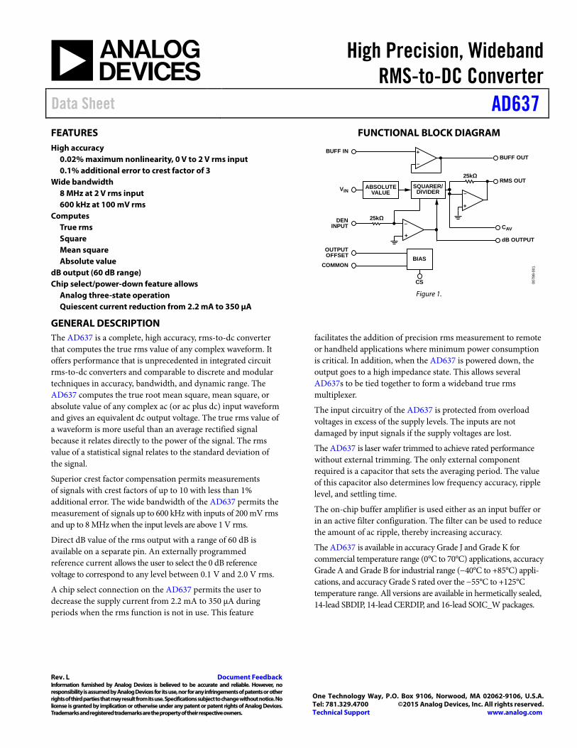
FUNCTIONAL BLOCK DIAGRAM
0078
8-00
1
VIN
25kΩ
25kΩ
ABSOLUTEVALUE
DENINPUT CAV
RMS OUT
BUFF INBUFF OUT
SQUARER/DIVIDER
BIASCOMMON
CS
OUTPUTOFFSET
dB OUTPUT
–
+
+
–
–
+
Figure 1.
GENERAL DESCRIPTION The AD637 is a complete, high accuracy, rms-to-dc converter that computes the true rms value of any complex waveform. It offers performance that is unprecedented in integrated circuit rms-to-dc converters and comparable to discrete and modular techniques in accuracy, bandwidth, and dynamic range. The AD637 computes the true root mean square, mean square, or absolute value of any complex ac (or ac plus dc) input waveform and gives an equivalent dc output voltage. The true rms value of a waveform is more useful than an average rectified signal because it relates directly to the power of the signal. The rms value of a statistical signal relates to the standard deviation of the signal.
Superior crest factor compensation permits measurements of signals with crest factors of up to 10 with less than 1% additional error. The wide bandwidth of the AD637 permits the measurement of signals up to 600 kHz with inputs of 200 mV rms and up to 8 MHz when the input levels are above 1 V rms.
Direct dB value of the rms output with a range of 60 dB is available on a separate pin. An externally programmed reference current allows the user to select the 0 dB reference voltage to correspond to any level between 0.1 V and 2.0 V rms.
A chip select connection on the AD637 permits the user to decrease the supply current from 2.2 mA to 350 µA during periods when the rms function is not in use. This feature
facilitates the addition of precision rms measurement to remote or handheld applications where minimum power consumption is critical. In addition, when the AD637 is powered down, the output goes to a high impedance state. This allows several AD637s to be tied together to form a wideband true rms multiplexer.
The input circuitry of the AD637 is protected from overload voltages in excess of the supply levels. The inputs are not damaged by input signals if the supply voltages are lost.
The AD637 is laser wafer trimmed to achieve rated performance without external trimming. The only external component required is a capacitor that sets the averaging period. The value of this capacitor also determines low frequency accuracy, ripple level, and settling time.
The on-chip buffer amplifier is used either as an input buffer or in an active filter configuration. The filter can be used to reduce the amount of ac ripple, thereby increasing accuracy.
The AD637 is available in accuracy Grade J and Grade K for commercial temperature range (0°C to 70°C) applications, accuracy Grade A and Grade B for industrial range (−40°C to +85°C) appli-cations, and accuracy Grade S rated over the −55°C to +125°C temperature range. All versions are available in hermetically sealed, 14-lead SBDIP, 14-lead CERDIP, and 16-lead SOIC_W packages.
Rev. L Document Feedback Information furnished by Analog Devices is believed to be accurate and reliable. However, no responsibility is assumed by Analog Devices for its use, nor for any infringements of patents or other rights of third parties that may result from its use. Specifications subject to change without notice. No license is granted by implication or otherwise under any patent or patent rights of Analog Devices. Trademarks and registered trademarks are the property of their respective owners.
One Technology Way, P.O. Box 9106, Norwood, MA 02062-9106, U.S.A. Tel: 781.329.4700 ©2015 Analog Devices, Inc. All rights reserved. Technical Support www.analog.com
AD637 Data Sheet
TABLE OF CONTENTS Features .............................................................................................. 1
Functional Block Diagram .............................................................. 1
General Description ......................................................................... 1
Revision History ............................................................................... 3
Specifications ..................................................................................... 4
Absolute Maximum Ratings .......................................................... 10
ESD Caution ................................................................................ 10
Pin Configurations and Function Descriptions ......................... 11
Theory of Operation ...................................................................... 12
Applications Information .............................................................. 13
Standard Connection ................................................................. 13
Chip Select ................................................................................... 13
Optional Trims for High Accuracy .......................................... 13
Offset Trim .............................................................................. 14
Scale Factor Trim ................................................................... 14
Choosing the Averaging Time Constant ................................. 14
Frequency Response .................................................................. 16
AC Measurement Accuracy and Crest Factor ........................ 17
Connection for dB Output ........................................................ 17
dB Calibration ............................................................................. 18
Low Frequency Measurements ................................................. 19
Vector Summation ..................................................................... 19
Evaluation Board ............................................................................ 21
Outline Dimensions ....................................................................... 24
Ordering Guide .......................................................................... 25
Rev. L | Page 2 of 25
Data Sheet AD637
REVISION HISTORY
4/15—Rev. K to Rev. L
Changes to Features Section, Figure 1, and General Description Section ................................................................................................ 1 Changes to Table 1 ............................................................................ 4 Added Table 2; Renumbered Sequentially ..................................... 6 Added Table 3 .................................................................................... 8 Changed Pin NC to Pin NIC (Throughout) ................................ 11 Changes to Theory of Operation Section and Figure 4 ............. 12 Changes to Figure 5......................................................................... 13 Changes to Optional Trims for High Accuracy Section and Figure 8; Added Offset Trim Section and Scale Factor Trim Section ............................................................................................... 14 Changes to Choosing the Averaging Time Constant and Figure 11 ........................................................................................... 15 Changes to Figure 20 ...................................................................... 19 Changes to Figure 21 ...................................................................... 20 Changes to Ordering Guide ........................................................... 26
2/11—Rev. J to Rev. K
Changes to Figure 15 ...................................................................... 11 Changes to Figure 16 ...................................................................... 12 Changes to Evaluation Board Section and Figure 23 ................. 16 Added Figure 24; Renumbered Sequentially ............................... 17 Changes to Figure 25 Through Figure 29 .................................... 17 Changes to Figure 30 ...................................................................... 18 Added Figure 31 .............................................................................. 18 Deleted Table 6; Renumbered Sequentially ................................. 18 Changes to Ordering Guide ........................................................... 20
4/07—Rev. I to Rev. J
Added Evaluation Board Section .................................................. 16 Updated Outline Dimensions ........................................................ 20
10/06—Rev. H to Rev. I
Changes to Table 1 ............................................................................ 3 Changes to Figure 4 .......................................................................... 7 Changes to Figure 7 .......................................................................... 9 Changes to Figure 16, Figure 18, and Figure 19 .......................... 12 Changes to Figure 20 ...................................................................... 13
12/05—Rev. G to Rev. H
Updated Format ................................................................. Universal Changes to Figure 1 .......................................................................... 1 Changes to Figure 11 ...................................................................... 10 Updated Outline Dimensions........................................................ 16 Changes to Ordering Guide ........................................................... 17
4/05—Rev. F to Rev. G
Updated Format ................................................................. Universal Changes to Figure 1 .......................................................................... 1 Changes to General Description ..................................................... 1 Deleted Product Highlights ............................................................. 1 Moved Figure 4 to Page .................................................................... 8 Changes to Figure 5 .......................................................................... 9 Changes to Figure 8 ........................................................................ 10 Changes to Figure 11, Figure 12, Figure 13, and Figure 14 ....... 11 Changes to Figure 19 ...................................................................... 14 Changes to Figure 20 ...................................................................... 14 Changes to Figure 21 ...................................................................... 16 Updated Outline Dimensions........................................................ 17 Changes to Ordering Guide ........................................................... 18
3/02—Rev. E to Rev. F
Edits to Ordering Guide ................................................................... 3
Rev. L | Page 3 of 25
AD637 Data Sheet
Rev. L | Page 4 of 25
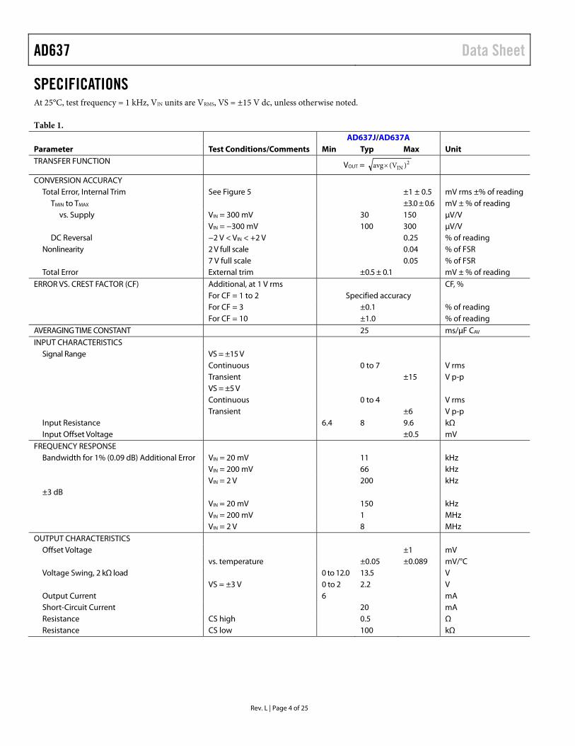
SPECIFICATIONS At 25°C, test frequency = 1 kHz, VIN units are VRMS, VS = ±15 V dc, unless otherwise noted.
Table 1.
Parameter Test Conditions/Comments AD637J/AD637A
Unit Min Typ Max TRANSFER FUNCTION VOUT = 2
IN )(V avg
CONVERSION ACCURACY Total Error, Internal Trim See Figure 5 ±1 ± 0.5 mV rms ±% of reading
TMIN to TMAX ±3.0 ± 0.6 mV ± % of reading vs. Supply VIN = 300 mV 30 150 μV/V VIN = −300 mV 100 300 μV/V
DC Reversal −2 V < VIN < +2 V 0.25 % of reading Nonlinearity 2 V full scale 0.04 % of FSR 7 V full scale 0.05 % of FSR Total Error External trim ±0.5 ± 0.1 mV ± % of reading
ERROR VS. CREST FACTOR (CF) Additional, at 1 V rms CF, % For CF = 1 to 2 Specified accuracy
For CF = 3 ±0.1 % of reading For CF = 10 ±1.0 % of reading
AVERAGING TIME CONSTANT 25 ms/μF CAV INPUT CHARACTERISTICS
Signal Range VS = ±15 V Continuous 0 to 7 V rms Transient ±15 V p-p VS = ±5 V Continuous 0 to 4 V rms Transient ±6 V p-p
Input Resistance 6.4 8 9.6 kΩ Input Offset Voltage ±0.5 mV
FREQUENCY RESPONSE Bandwidth for 1% (0.09 dB) Additional Error VIN = 20 mV 11 kHz
VIN = 200 mV 66 kHz VIN = 2 V 200 kHz
±3 dB VIN = 20 mV 150 kHz VIN = 200 mV 1 MHz VIN = 2 V 8 MHz
OUTPUT CHARACTERISTICS Offset Voltage ±1 mV
vs. temperature ±0.05 ±0.089 mV/°C Voltage Swing, 2 kΩ load 0 to 12.0 13.5 V VS = ±3 V 0 to 2 2.2 V Output Current 6 mA Short-Circuit Current 20 mA Resistance CS high 0.5 Ω Resistance CS low 100 kΩ
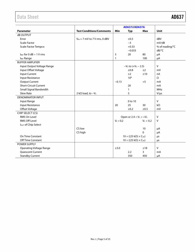
Data Sheet AD637
Parameter Test Conditions/Comments AD637J/AD637A
Unit Min Typ Max dB OUTPUT
Error VIN = 7 mV to 7 V rms, 0 dBV ±0.5 dBV Scale Factor −3 mV/dB Scale Factor Tempco +0.33 % of reading/°C −0.033 dB/°C IREF for 0 dB = 1 V rms 5 20 80 µA IREF Range 1 100 µA
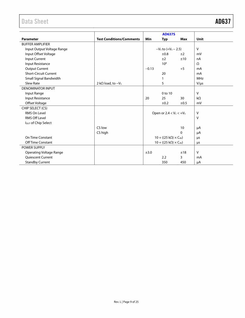
BUFFER AMPLIFIER Input Output Voltage Range −VS to (+VS − 2.5) V Input Offset Voltage ±0.8 ±2 mV Input Current ±2 ±10 nA Input Resistance 108 Ω Output Current −0.13 +5 mA Short-Circuit Current 20 mA Small Signal Bandwidth 1 MHz Slew Rate 2 kΩ load, to −VS 5 V/µs
DENOMINATOR INPUT Input Range 0 to 10 V Input Resistance 20 25 30 kΩ Offset Voltage ±0.2 ±0.5 mV
CHIP SELECT (CS) RMS On Level Open or 2.4 < VC < +VS V RMS Off Level VC < 0.2 VC < 0.2 V IOUT of Chip Select
CS low 10 µA CS high 0 µA
On Time Constant 10 + ((25 kΩ) × CAV) µs Off Time Constant 10 + ((25 kΩ) × CAV) µs
POWER SUPPLY Operating Voltage Range ±3.0 ±18 V Quiescent Current 2.2 3 mA Standby Current 350 450 µA
Rev. L | Page 5 of 25
AD637 Data Sheet
Rev. L | Page 6 of 25
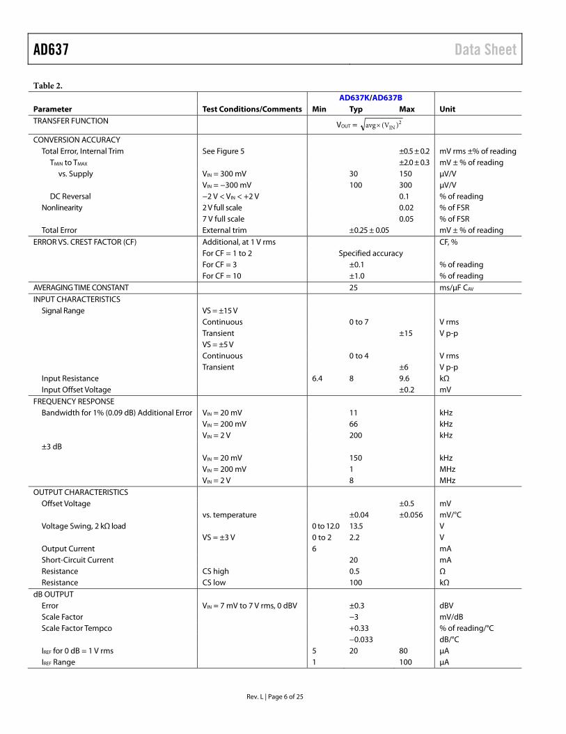
Table 2.
Parameter Test Conditions/Comments AD637K/AD637B
Unit Min Typ Max TRANSFER FUNCTION VOUT = 2
IN )(V avg
CONVERSION ACCURACY Total Error, Internal Trim See Figure 5 ±0.5 ± 0.2 mV rms ±% of reading
TMIN to TMAX ±2.0 ± 0.3 mV ± % of reading vs. Supply VIN = 300 mV 30 150 μV/V VIN = −300 mV 100 300 μV/V
DC Reversal −2 V < VIN < +2 V 0.1 % of reading Nonlinearity 2 V full scale 0.02 % of FSR 7 V full scale 0.05 % of FSR Total Error External trim ±0.25 ± 0.05 mV ± % of reading
ERROR VS. CREST FACTOR (CF) Additional, at 1 V rms CF, % For CF = 1 to 2 Specified accuracy
For CF = 3 ±0.1 % of reading For CF = 10 ±1.0 % of reading
AVERAGING TIME CONSTANT 25 ms/μF CAV INPUT CHARACTERISTICS
Signal Range VS = ±15 V Continuous 0 to 7 V rms Transient ±15 V p-p VS = ±5 V Continuous 0 to 4 V rms Transient ±6 V p-p
Input Resistance 6.4 8 9.6 kΩ Input Offset Voltage ±0.2 mV
FREQUENCY RESPONSE Bandwidth for 1% (0.09 dB) Additional Error VIN = 20 mV 11 kHz
VIN = 200 mV 66 kHz VIN = 2 V 200 kHz
±3 dB VIN = 20 mV 150 kHz VIN = 200 mV 1 MHz VIN = 2 V 8 MHz
OUTPUT CHARACTERISTICS Offset Voltage ±0.5 mV
vs. temperature ±0.04 ±0.056 mV/°C Voltage Swing, 2 kΩ load 0 to 12.0 13.5 V VS = ±3 V 0 to 2 2.2 V Output Current 6 mA Short-Circuit Current 20 mA Resistance CS high 0.5 Ω Resistance CS low 100 kΩ
dB OUTPUT Error VIN = 7 mV to 7 V rms, 0 dBV ±0.3 dBV Scale Factor −3 mV/dB Scale Factor Tempco +0.33 % of reading/°C −0.033 dB/°C IREF for 0 dB = 1 V rms 5 20 80 μA IREF Range 1 100 μA
Data Sheet AD637
Rev. L | Page 7 of 25
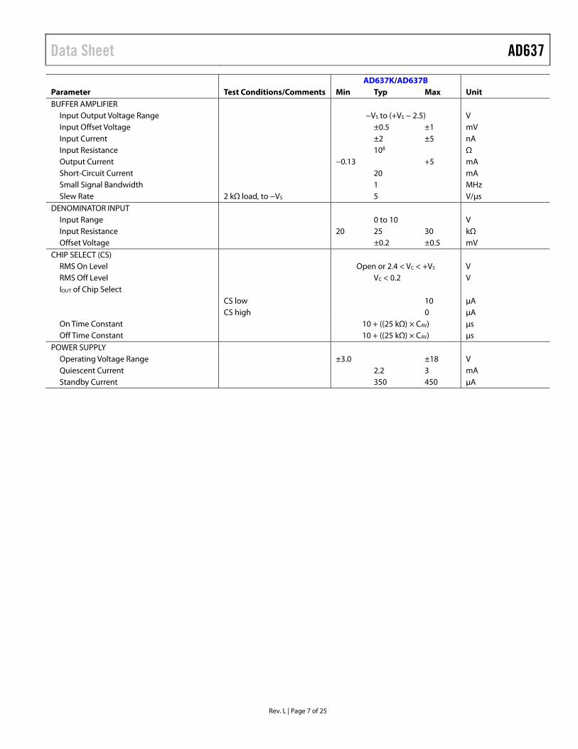
Parameter Test Conditions/Comments AD637K/AD637B
Unit Min Typ Max BUFFER AMPLIFIER
Input Output Voltage Range −VS to (+VS − 2.5) V Input Offset Voltage ±0.5 ±1 mV Input Current ±2 ±5 nA Input Resistance 108 Ω Output Current −0.13 +5 mA Short-Circuit Current 20 mA Small Signal Bandwidth 1 MHz Slew Rate 2 kΩ load, to −VS 5 V/μs
DENOMINATOR INPUT Input Range 0 to 10 V Input Resistance 20 25 30 kΩ Offset Voltage ±0.2 ±0.5 mV
CHIP SELECT (CS) RMS On Level Open or 2.4 < VC < +VS V RMS Off Level VC < 0.2 V IOUT of Chip Select
CS low 10 μA CS high 0 μA
On Time Constant 10 + ((25 kΩ) × CAV) μs Off Time Constant 10 + ((25 kΩ) × CAV) μs
POWER SUPPLY Operating Voltage Range ±3.0 ±18 V Quiescent Current 2.2 3 mA Standby Current 350 450 μA
AD637 Data Sheet
Rev. L | Page 8 of 25
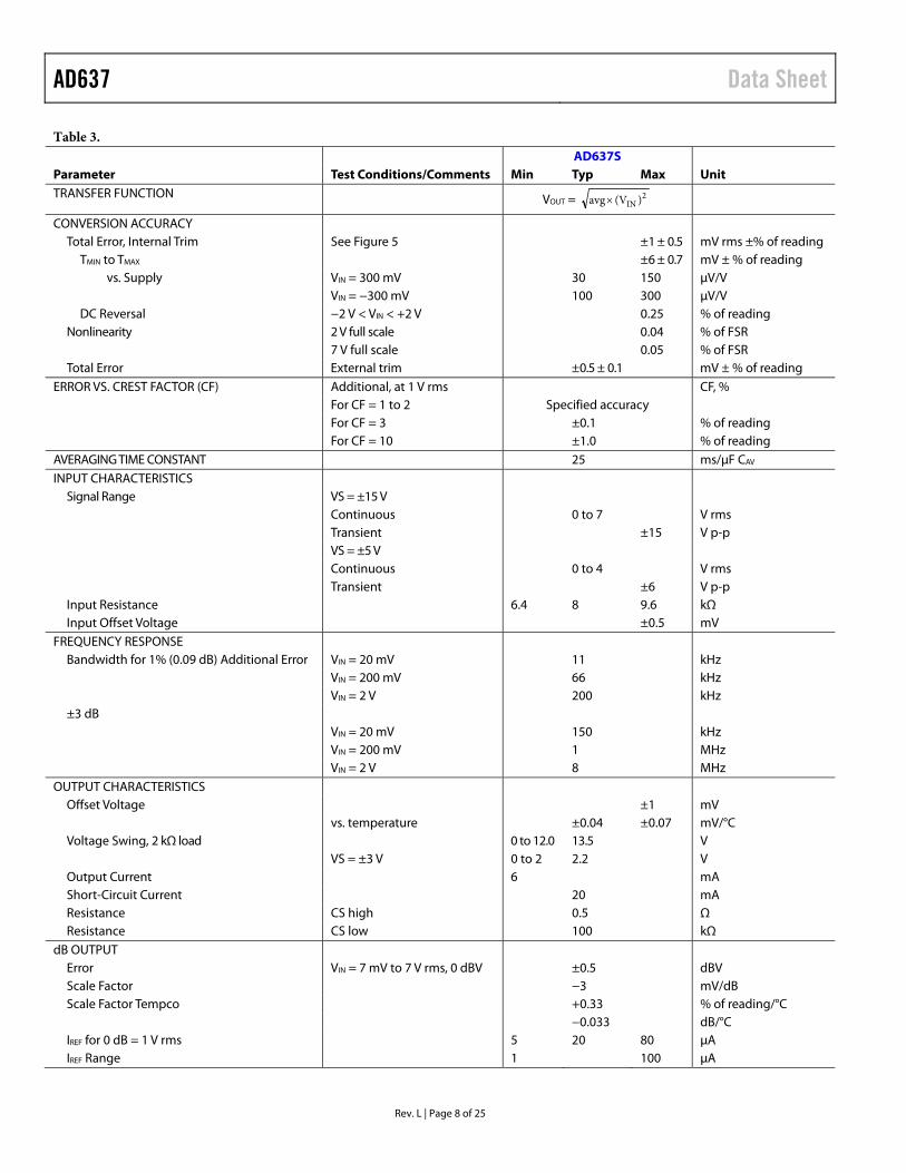
Table 3.
Parameter Test Conditions/Comments AD637S
Unit Min Typ Max TRANSFER FUNCTION VOUT = 2
IN )(V avg
CONVERSION ACCURACY Total Error, Internal Trim See Figure 5 ±1 ± 0.5 mV rms ±% of reading
TMIN to TMAX ±6 ± 0.7 mV ± % of reading vs. Supply VIN = 300 mV 30 150 μV/V VIN = −300 mV 100 300 μV/V
DC Reversal −2 V < VIN < +2 V 0.25 % of reading Nonlinearity 2 V full scale 0.04 % of FSR 7 V full scale 0.05 % of FSR Total Error External trim ±0.5 ± 0.1 mV ± % of reading
ERROR VS. CREST FACTOR (CF) Additional, at 1 V rms CF, % For CF = 1 to 2 Specified accuracy
For CF = 3 ±0.1 % of reading For CF = 10 ±1.0 % of reading
AVERAGING TIME CONSTANT 25 ms/μF CAV INPUT CHARACTERISTICS
Signal Range VS = ±15 V Continuous 0 to 7 V rms Transient ±15 V p-p VS = ±5 V Continuous 0 to 4 V rms Transient ±6 V p-p
Input Resistance 6.4 8 9.6 kΩ Input Offset Voltage ±0.5 mV
FREQUENCY RESPONSE Bandwidth for 1% (0.09 dB) Additional Error VIN = 20 mV 11 kHz
VIN = 200 mV 66 kHz VIN = 2 V 200 kHz
±3 dB VIN = 20 mV 150 kHz VIN = 200 mV 1 MHz VIN = 2 V 8 MHz
OUTPUT CHARACTERISTICS Offset Voltage ±1 mV
vs. temperature ±0.04 ±0.07 mV/°C Voltage Swing, 2 kΩ load 0 to 12.0 13.5 V VS = ±3 V 0 to 2 2.2 V Output Current 6 mA Short-Circuit Current 20 mA Resistance CS high 0.5 Ω Resistance CS low 100 kΩ
dB OUTPUT Error VIN = 7 mV to 7 V rms, 0 dBV ±0.5 dBV Scale Factor −3 mV/dB Scale Factor Tempco +0.33 % of reading/°C −0.033 dB/°C IREF for 0 dB = 1 V rms 5 20 80 μA IREF Range 1 100 μA
Data Sheet AD637
Rev. L | Page 9 of 25
Parameter Test Conditions/Comments AD637S
Unit Min Typ Max BUFFER AMPLIFIER
Input Output Voltage Range −VS to (+VS − 2.5) V Input Offset Voltage ±0.8 ±2 mV Input Current ±2 ±10 nA Input Resistance 108 Ω Output Current −0.13 +5 mA Short-Circuit Current 20 mA Small Signal Bandwidth 1 MHz Slew Rate 2 kΩ load, to −VS 5 V/μs
DENOMINATOR INPUT Input Range 0 to 10 V Input Resistance 20 25 30 kΩ Offset Voltage ±0.2 ±0.5 mV
CHIP SELECT (CS) RMS On Level Open or 2.4 < VC < +VS V RMS Off Level V IOUT of Chip Select
CS low 10 μA CS high 0 μA
On Time Constant 10 + ((25 kΩ) × CAV) μs Off Time Constant 10 + ((25 kΩ) × CAV) μs
POWER SUPPLY Operating Voltage Range ±3.0 ±18 V Quiescent Current 2.2 3 mA Standby Current 350 450 μA
AD637 Data Sheet
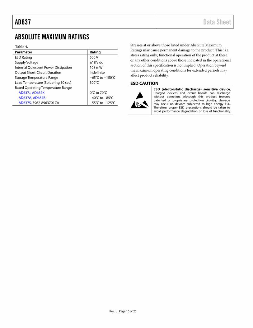
ABSOLUTE MAXIMUM RATINGS Table 4. Parameter Rating ESD Rating 500 V Supply Voltage ±18 V dc Internal Quiescent Power Dissipation 108 mW Output Short-Circuit Duration Indefinite Storage Temperature Range −65°C to +150°C Lead Temperature (Soldering 10 sec) 300°C Rated Operating Temperature Range
AD637J, AD637K 0°C to 70°C AD637A, AD637B −40°C to +85°C AD637S, 5962-8963701CA −55°C to +125°C
Stresses at or above those listed under Absolute Maximum Ratings may cause permanent damage to the product. This is a stress rating only; functional operation of the product at these or any other conditions above those indicated in the operational section of this specification is not implied. Operation beyond the maximum operating conditions for extended periods may affect product reliability.
ESD CAUTION
Rev. L | Page 10 of 25
Data Sheet AD637
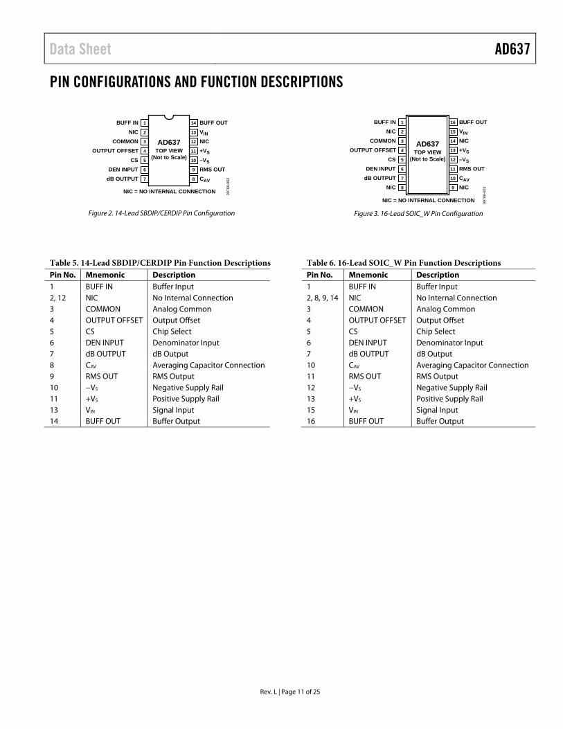
PIN CONFIGURATIONS AND FUNCTION DESCRIPTIONS
BUFF IN 1
NIC 2
COMMON 3
OUTPUT OFFSET 4
BUFF OUT14
VIN13
NIC12
+VS11
CS 5 –VS10
DEN INPUT 6 RMS OUT9
dB OUTPUT 7 CAV8
NIC = NO INTERNAL CONNECTION
AD637TOP VIEW
(Not to Scale)
0078
8-00
2
Figure 2. 14-Lead SBDIP/CERDIP Pin Configuration
BUFF IN 1
NIC 2
COMMON 3
OUTPUT OFFSET 4
BUFF OUT16
VIN15
NIC14
+VS13
CS 5 –VS12
DEN INPUT 6 RMS OUT11
dB OUTPUT 7 CAV10
NIC 8 NIC9
NIC = NO INTERNAL CONNECTION
AD637TOP VIEW
(Not to Scale)
0078
8-00
3
Figure 3. 16-Lead SOIC_W Pin Configuration
Table 5. 14-Lead SBDIP/CERDIP Pin Function Descriptions Pin No. Mnemonic Description 1 BUFF IN Buffer Input 2, 12 NIC No Internal Connection 3 COMMON Analog Common 4 OUTPUT OFFSET Output Offset 5 CS Chip Select 6 DEN INPUT Denominator Input 7 dB OUTPUT dB Output 8 CAV Averaging Capacitor Connection 9 RMS OUT RMS Output 10 −VS Negative Supply Rail 11 +VS Positive Supply Rail 13 VIN Signal Input 14 BUFF OUT Buffer Output
Table 6. 16-Lead SOIC_W Pin Function Descriptions Pin No. Mnemonic Description 1 BUFF IN Buffer Input 2, 8, 9, 14 NIC No Internal Connection 3 COMMON Analog Common 4 OUTPUT OFFSET Output Offset 5 CS Chip Select 6 DEN INPUT Denominator Input 7 dB OUTPUT dB Output 10 CAV Averaging Capacitor Connection 11 RMS OUT RMS Output 12 −VS Negative Supply Rail 13 +VS Positive Supply Rail 15 VIN Signal Input 16 BUFF OUT Buffer Output
Rev. L | Page 11 of 25
AD637 Data Sheet
Rev. L | Page 12 of 25
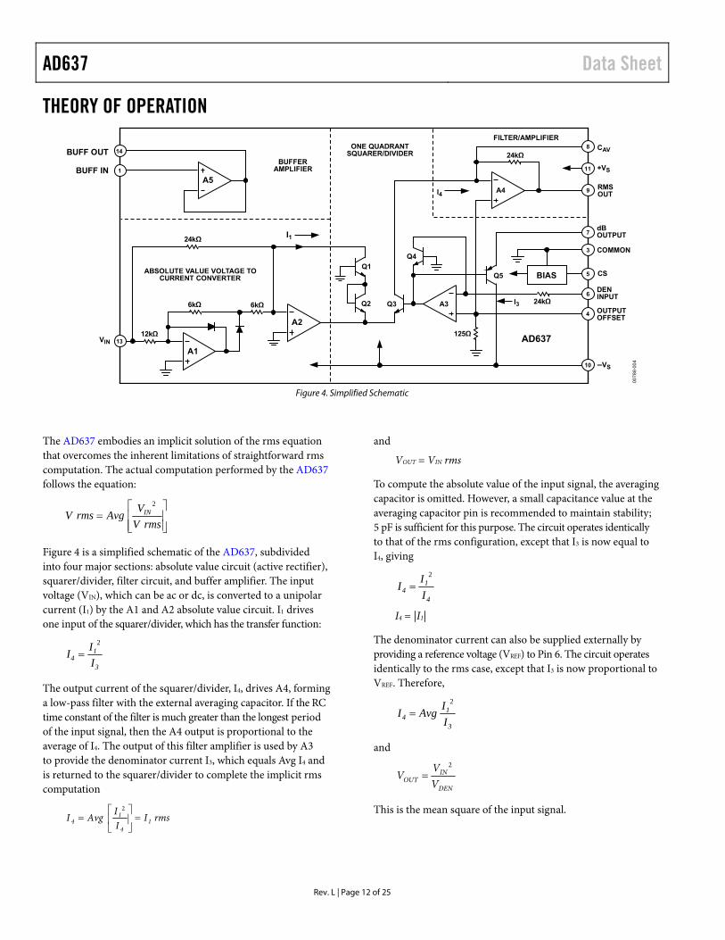
THEORY OF OPERATION FILTER/AMPLIFIER
24kΩ
24kΩ
ONE QUADRANTSQUARER/DIVIDER
BUFFERAMPLIFIER
Q1
Q2 Q3
Q4
125Ω
6kΩ6kΩ
12kΩ
24kΩ
A5
A1
A2
ABSOLUTE VALUE VOLTAGE TOCURRENT CONVERTER
I1
I3
I4 A4
A3
BIASQ5
CAV
+VS
RMSOUT
COMMON
CS
DENINPUT
OUTPUTOFFSET
dBOUTPUT
AD637
BUFF OUT
BUFF IN
–VS
14
1
13
10
4
6
5
3
7
9
11
8
VIN
0078
8-00
4
Figure 4. Simplified Schematic
The AD637 embodies an implicit solution of the rms equation that overcomes the inherent limitations of straightforward rms computation. The actual computation performed by the AD637 follows the equation:
rmsV
VAvgrmsV IN
2
Figure 4 is a simplified schematic of the AD637, subdivided into four major sections: absolute value circuit (active rectifier), squarer/divider, filter circuit, and buffer amplifier. The input voltage (VIN), which can be ac or dc, is converted to a unipolar current (I1) by the A1 and A2 absolute value circuit. I1 drives one input of the squarer/divider, which has the transfer function:
3
14 I
II
2
The output current of the squarer/divider, I4, drives A4, forming a low-pass filter with the external averaging capacitor. If the RC time constant of the filter is much greater than the longest period of the input signal, then the A4 output is proportional to the average of I4. The output of this filter amplifier is used by A3 to provide the denominator current I3, which equals Avg I4 and is returned to the squarer/divider to complete the implicit rms computation
rmsIIIAvgI 1
4
14
2
and
VOUT = VIN rms
To compute the absolute value of the input signal, the averaging capacitor is omitted. However, a small capacitance value at the averaging capacitor pin is recommended to maintain stability; 5 pF is sufficient for this purpose. The circuit operates identically to that of the rms configuration, except that I3 is now equal to I4, giving
4
14 I
II
2
I4 = |I1|
The denominator current can also be supplied externally by providing a reference voltage (VREF) to Pin 6. The circuit operates identically to the rms case, except that I3 is now proportional to VREF. Therefore,
3
14 I
IAvgI
2
and
DEN
INOUT V
VV
2
This is the mean square of the input signal.
Data Sheet AD637
APPLICATIONS INFORMATION STANDARD CONNECTION The AD637 is simple to connect for a majority of rms measurements. In the standard rms connection shown in Figure 5, only a single external capacitor is required to set the averaging time constant. In this configuration, the AD637 computes the true rms of any input signal. An averaging error, the magnitude of which is dependent on the value of the averaging capacitor, is present at low frequencies. For example, if the filter capacitor, CAV, is 4 µF, the error is 0.1% at 10 Hz and increases to 1% at 3 Hz. To measure ac signals, the AD637 can be ac-coupled by adding a nonpolar capacitor in series with the input, as shown in Figure 5.
0078
8-00
5
1
25kΩ
DENINPUT
CAV
BUFF INBUFF OUT
SQUARER/DIVIDER
CS
dBOUTPUT
3 COMMON
ABSOLUTEVALUE
BIAS
2 NIC
4OUTPUTOFFSET
4.7kΩ
+VS
5
25kΩ6
7 8
9
10
11
12NIC
13
14NC
–VS–VS
+VS+VS
VIN
VOUT = VIN2
(OPTIONAL)
VIN
CAV+
AD637
RMSOUT–
+–
+
–
+
NIC = NO INTERNAL CONNECTION Figure 5. Standard RMS Connection
The performance of the AD637 is tolerant of minor variations in the power supply voltages; however, if the supplies used exhibit a considerable amount of high frequency ripple, it is advisable to bypass both supplies to ground through a 0.1 µF ceramic disc capacitor placed as close to the device as possible.
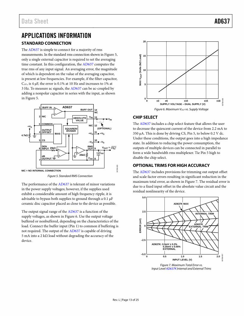
The output signal range of the AD637 is a function of the supply voltages, as shown in Figure 6. Use the output voltage buffered or nonbuffered, depending on the characteristics of the load. Connect the buffer input (Pin 1) to common if buffering is not required. The output of the AD637 is capable of driving 5 mA into a 2 kΩ load without degrading the accuracy of the device.
20
15
00
10
5
0078
8-00
6
SUPPLY VOLTAGE – DUAL SUPPLY (V)±3 ±5 ±10 ±15 ±18
MA
X V O
UT
(Vol
ts 2
kΩ L
oad)
Figure 6. Maximum VOUT vs. Supply Voltage
CHIP SELECT The AD637 includes a chip select feature that allows the user to decrease the quiescent current of the device from 2.2 mA to 350 µA. This is done by driving CS, Pin 5, to below 0.2 V dc. Under these conditions, the output goes into a high impedance state. In addition to reducing the power consumption, the outputs of multiple devices can be connected in parallel to form a wide bandwidth rms multiplexer. Tie Pin 5 high to disable the chip select.
OPTIONAL TRIMS FOR HIGH ACCURACY The AD637 includes provisions for trimming out output offset and scale factor errors resulting in significant reduction in the maximum total error, as shown in Figure 7. The residual error is due to a fixed input offset in the absolute value circuit and the residual nonlinearity of the device.
5.0
2.5
–5.00 2.00.5
ERR
OR
(mV)
1.0
0
–2.5
1.5
AD637K MAX
INTERNAL TRIM
0078
8-00
7AD637K
EXTERNAL TRIM
AD637K: 0.5mV ± 0.2% 0.25mV ± 0.05% EXTERNAL
INPUT LEVEL (V) Figure 7. Maximum Total Error vs.
Input Level AD637K Internal and External Trims
Rev. L | Page 13 of 25
AD637 Data Sheet Referring to Figure 8 for optional external gain and offset trim schematic. The following sections describe trimming for greater accuracy in detail.
Offset Trim
Ground the input signal (VIN) and adjust R1 until the output voltage at Pin 9 measures 0 V. Alternatively, apply the least expected value of VIN.at the input VIN and adjust R1 until the dc output voltage at Pin 9 measures the same value as the rms input.
Scale Factor Trim
Insert Resistor R4 in series with the input to decrease the range of the scale factor. Connect a precision source to Pin 13 and adjust the output for the desired full-scale input to VIN, using either a calibrated dc or 1 kHz ac voltage, and adjust Resistor R3 to give the correct output at Pin 9 (that is, 1 V rms at the input results in a dc output voltage of 1.000 V dc). A 2 V p-p sine wave input yields 0.707 V dc at the output. Remaining errors are due to the nonlinearity.
25kΩ
–VS–VS –VS
1
25kΩ
DENINPUT
CAV
BUFF IN BUFFOUT
CS
dBOUTPUT
3 COMMON
ABSOLUTEVALUE
BIAS
2 NIC
4OUTPUTOFFSET
4.7kΩ 5
6
7 8
9
10
11
12NIC
13
14NC
VIN VIN
R4147Ω
CAV+
R31kΩ
R21MΩR1
50kΩ
+VS
+VS+VS
+VS
OUTPUTOFFSET
TRIM
SCALE FACTOR TRIM
AD637
RMSOUT
SQUARER/DIVIDER
–+
–+
RMSOUT
–+
0078
8-00
8
NIC = NO INTERNAL CONNECTION Figure 8. Optional External Gain and Offset Trims
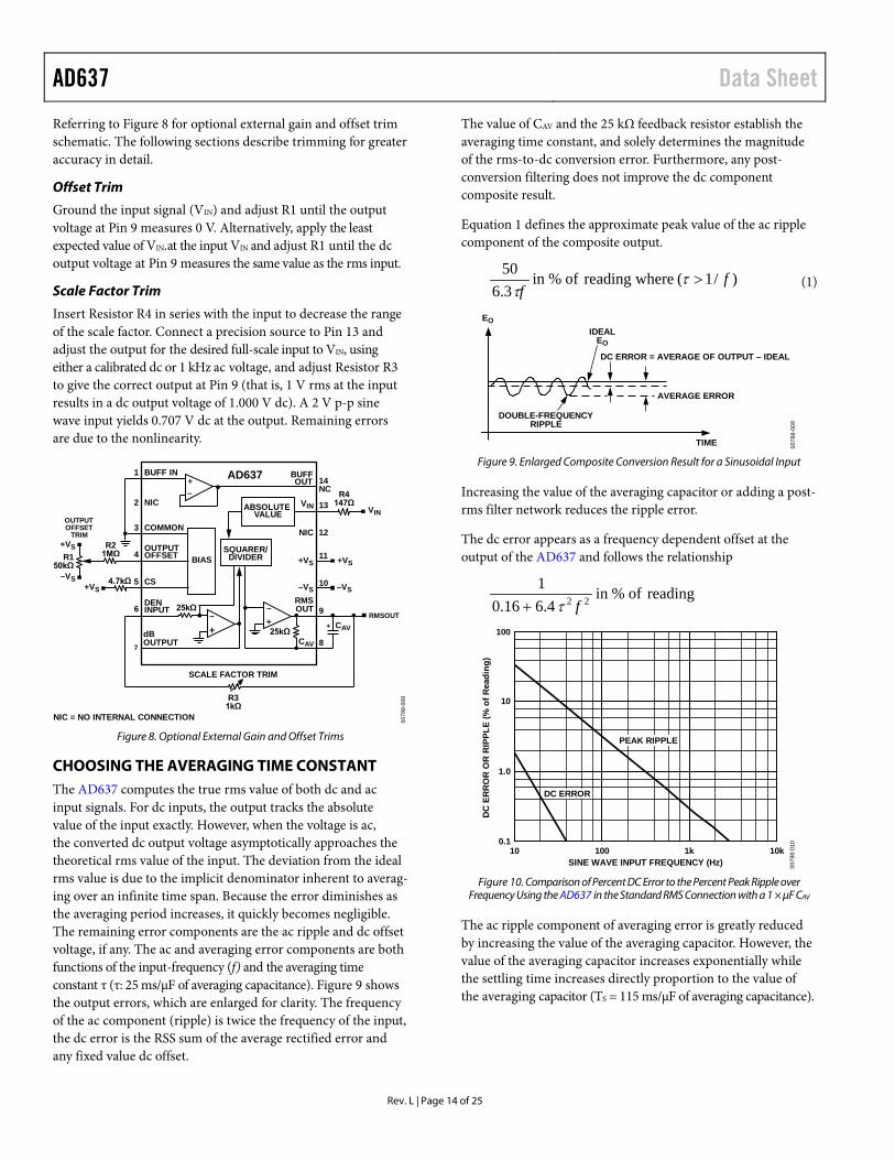
CHOOSING THE AVERAGING TIME CONSTANT The AD637 computes the true rms value of both dc and ac input signals. For dc inputs, the output tracks the absolute value of the input exactly. However, when the voltage is ac, the converted dc output voltage asymptotically approaches the theoretical rms value of the input. The deviation from the ideal rms value is due to the implicit denominator inherent to averag-ing over an infinite time span. Because the error diminishes as the averaging period increases, it quickly becomes negligible. The remaining error components are the ac ripple and dc offset voltage, if any. The ac and averaging error components are both functions of the input-frequency (f) and the averaging time constant τ (τ: 25 ms/µF of averaging capacitance). Figure 9 shows the output errors, which are enlarged for clarity. The frequency of the ac component (ripple) is twice the frequency of the input, the dc error is the RSS sum of the average rectified error and any fixed value dc offset.
The value of CAV and the 25 kΩ feedback resistor establish the averaging time constant, and solely determines the magnitude of the rms-to-dc conversion error. Furthermore, any post-conversion filtering does not improve the dc component composite result.
Equation 1 defines the approximate peak value of the ac ripple component of the composite output.
)/1(wherereadingof%in3.650 f
f>τ
τ (1)
DOUBLE-FREQUENCYRIPPLE
EO
TIME
AVERAGE ERROR
IDEALEO
0078
8-00
9
DC ERROR = AVERAGE OF OUTPUT – IDEAL
Figure 9. Enlarged Composite Conversion Result for a Sinusoidal Input
Increasing the value of the averaging capacitor or adding a post-rms filter network reduces the ripple error.
The dc error appears as a frequency dependent offset at the output of the AD637 and follows the relationship
readingof%in4.616.0
122 fτ+
SINE WAVE INPUT FREQUENCY (Hz)
100
0.1
1.0
10 10k
DC
ER
RO
R O
R R
IPPL
E (%
of R
eadi
ng)
1k100
10
DC ERROR
PEAK RIPPLE
0078
8-01
0
Figure 10. Comparison of Percent DC Error to the Percent Peak Ripple over
Frequency Using the AD637 in the Standard RMS Connection with a 1 × µF CAV
The ac ripple component of averaging error is greatly reduced by increasing the value of the averaging capacitor. However, the value of the averaging capacitor increases exponentially while the settling time increases directly proportion to the value of the averaging capacitor (TS = 115 ms/µF of averaging capacitance).
Rev. L | Page 14 of 25
Data Sheet AD637 A preferable ripple reduction method is to use a post conversion one or two-pole low-pass filter, as shown in Figure 11. Usually a single-pole filter gives the best overall compromise between ripple and settling time. Use the two-pole Sallen-Key for more ripple attenuation.
1
25kΩ
DENINPUT
BUFF IN BUFFOUT
SQUARER/DIVIDER
CS
dBOUTPUT
3 COMMON
ABSOLUTEVALUE
BIAS
2 NIC
4OUTPUTOFFSET
4.7kΩ+VS
5
25kΩ6
78
9
10
11
12NIC
13
14
VIN VIN
CAV
CAV
+
RX24kΩ
DIVIDER
C2
24kΩ
+
C3+
RMSOUT
AD637
FOR A 1 POLEFILTER SHORT RXAND REMOVE C3
–
+
–
+
–
+
–VS –VS
+VS +VS
0078
8-01
1
NIC = NO INTERNAL CONNECTION Figure 11. 2-Pole Sallen-Key Filter
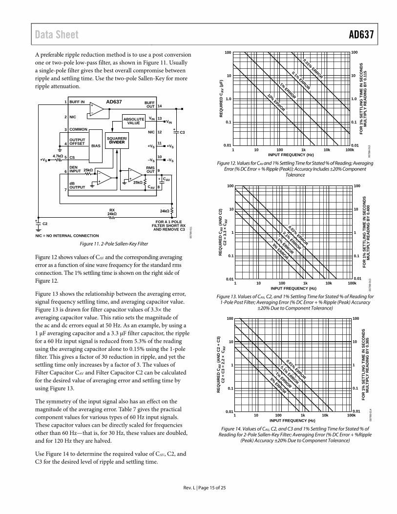
Figure 12 shows values of CAV and the corresponding averaging error as a function of sine wave frequency for the standard rms connection. The 1% settling time is shown on the right side of Figure 12.
Figure 13 shows the relationship between the averaging error, signal frequency settling time, and averaging capacitor value. Figure 13 is drawn for filter capacitor values of 3.3× the averaging capacitor value. This ratio sets the magnitude of the ac and dc errors equal at 50 Hz. As an example, by using a 1 µF averaging capacitor and a 3.3 µF filter capacitor, the ripple for a 60 Hz input signal is reduced from 5.3% of the reading using the averaging capacitor alone to 0.15% using the 1-pole filter. This gives a factor of 30 reduction in ripple, and yet the settling time only increases by a factor of 3. The values of Filter Capacitor CAV and Filter Capacitor C2 can be calculated for the desired value of averaging error and settling time by using Figure 13.
The symmetry of the input signal also has an effect on the magnitude of the averaging error. Table 7 gives the practical component values for various types of 60 Hz input signals. These capacitor values can be directly scaled for frequencies other than 60 Hz—that is, for 30 Hz, these values are doubled, and for 120 Hz they are halved.
Use Figure 14 to determine the required value of CAV, C2, and C3 for the desired level of ripple and settling time.
FOR
1%
SET
TLIN
G T
IME
IN S
ECO
ND
SM
ULT
IPLY
REA
DIN
G B
Y 0.
115
INPUT FREQUENCY (Hz)
100
0.011 100k10 100 1k 10k
10
1.0
0.1
10% ERROR
1% ERROR
0.1% ERROR
0.01% ERROR
100
0.01
10
1.0
0.1
0078
8-01
2
REQ
UIR
ED C
AV
(µF)
Figure 12. Values for CAV and 1% Settling Time for Stated % of Reading; Averaging
Error (% DC Error + % Ripple (Peak)); Accuracy Includes ±20% Component Tolerance
INPUT FREQUENCY (Hz)
100
0.011 100k10 100 1k 10k
10
1
0.1
5% ERROR
1% ERROR
0.1% ERROR
0.01% ERROR
100
0.01
10
1
0.1
0078
8-01
3
REQ
UIR
ED C
AV (A
ND
C2)
C2
= 3.
3 ×
CAV
FOR
1%
SET
TLIN
G T
IME
IN S
ECO
ND
SM
ULT
IPLY
REA
DIN
G B
Y 0.
400
Figure 13. Values of CAV, C2, and 1% Settling Time for Stated % of Reading for
1-Pole Post Filter; Averaging Error (% DC Error + % Ripple (Peak) Accuracy ±20% Due to Component Tolerance)
INPUT FREQUENCY (Hz)
100
0.011 100k10 100 1k 10k
10
1
0.1
5% ERROR
1% ERROR
0.1% ERROR
0.01% ERROR
100
0.01
10
1
0.1
0078
8-01
4
REQ
UIR
ED C
AV (A
ND
C2
+ C
3)C
2 =
C3
= 2.
2 ×
CAV
FOR
1%
SET
TLIN
G T
IME
IN S
ECO
ND
SM
UL T
IPLY
REA
DIN
G B
Y 0.
365
Figure 14. Values of CAV, C2, and C3 and 1% Settling Time for Stated % of
Reading for 2-Pole Sallen-Key Filter; Averaging Error (% DC Error + %Ripple (Peak) Accuracy ±20% Due to Component Tolerance)
Rev. L | Page 15 of 25
AD637 Data Sheet
Rev. L | Page 16 of 25
Table 7. Practical Values of CAV and C2 for Various Input Waveforms
Input Waveform and Period
Absolute Value Circuit Waveform and Period
Minimum R × CAV Time Constant
Recommended Standard Values for CAV and C2 for 1% Averaging Error @ 60 Hz with T = 16.6 ms 1% Settling
Time CAV (μF) C2 (μF)
Symmetrical Sine Wave
A 0V
T
1/2T
1/2T 0.47 1.5 181 ms
Sine Wave with dc Offset
B0V
T
T
T 0.82 2.7 325 ms
Pulse Train Waveform
C T2 0V
T
T2
T
10 (T − T2) 6.8 22 2.67 sec
D T2 0V
T
T2
T
10 (T − 2T2) 5.6 18 2.17 sec
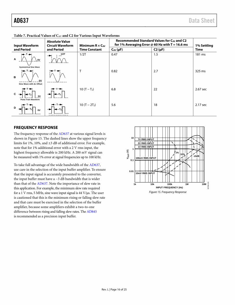
FREQUENCY RESPONSE The frequency response of the AD637 at various signal levels is shown in Figure 15. The dashed lines show the upper frequency limits for 1%, 10%, and ±3 dB of additional error. For example, note that for 1% additional error with a 2 V rms input, the highest frequency allowable is 200 kHz. A 200 mV signal can be measured with 1% error at signal frequencies up to 100 kHz.
To take full advantage of the wide bandwidth of the AD637, use care in the selection of the input buffer amplifier. To ensure that the input signal is accurately presented to the converter, the input buffer must have a −3 dB bandwidth that is wider than that of the AD637. Note the importance of slew rate in this application. For example, the minimum slew rate required for a 1 V rms, 5 MHz, sine wave input signal is 44 V/μs. The user is cautioned that this is the minimum rising or falling slew rate and that care must be exercised in the selection of the buffer amplifier, because some amplifiers exhibit a two-to-one difference between rising and falling slew rates. The AD845 is recommended as a precision input buffer.
10
1k 10M10k
V OUT
(V)
100k 1M
1
0.1
0.01
1%±3dB
10%
7V RMS INPUT2V RMS INPUT1V RMS INPUT
100mV RMS INPUT
10mV RMS INPUT
0078
8-01
5
INPUT FREQUENCY (Hz) Figure 15. Frequency Response
Data Sheet AD637
Rev. L | Page 17 of 25
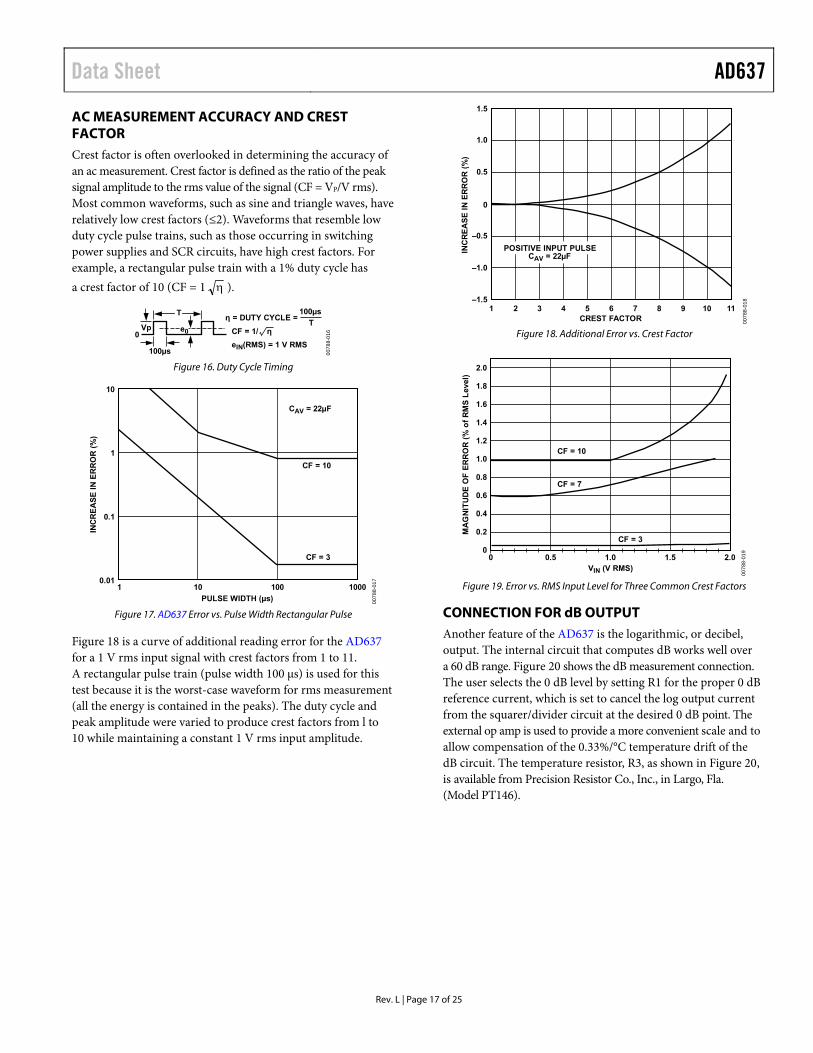
AC MEASUREMENT ACCURACY AND CREST FACTOR Crest factor is often overlooked in determining the accuracy of an ac measurement. Crest factor is defined as the ratio of the peak signal amplitude to the rms value of the signal (CF = VP/V rms). Most common waveforms, such as sine and triangle waves, have relatively low crest factors (≤2). Waveforms that resemble low duty cycle pulse trains, such as those occurring in switching power supplies and SCR circuits, have high crest factors. For example, a rectangular pulse train with a 1% duty cycle has a crest factor of 10 (CF = 1 ).
0Vp
TT
CF = 1/ η
eIN(RMS) = 1 V RMS
100µsη = DUTY CYCLE =
100µs
e000
788-
016
Figure 16. Duty Cycle Timing
PULSE WIDTH (µs)
10
1
0.011 100010
INC
RE
AS
E I
N E
RR
OR
(%
)
100
0.1
CF = 10
CF = 3
0078
8-01
7
CAV = 22µF
Figure 17. AD637 Error vs. Pulse Width Rectangular Pulse
Figure 18 is a curve of additional reading error for the AD637 for a 1 V rms input signal with crest factors from 1 to 11. A rectangular pulse train (pulse width 100 μs) is used for this test because it is the worst-case waveform for rms measurement (all the energy is contained in the peaks). The duty cycle and peak amplitude were varied to produce crest factors from l to 10 while maintaining a constant 1 V rms input amplitude.
CREST FACTOR
1.5
0
–1.51 112
INC
RE
AS
E I
N E
RR
OR
(%
)
3 7 8 9 10
1.0
0.5
–0.5
–1.0
0078
8-01
8
4 5 6
POSITIVE INPUT PULSECAV = 22µF
Figure 18. Additional Error vs. Crest Factor
2.0
1.8
02.00.5 1.0 1.5
1.2
0.6
0.4
0.2
1.6
1.4
0.8
1.0CF = 10
CF = 7
CF = 3
0
0078
8-01
9
VIN (V RMS)
MA
GN
ITU
DE
OF
ER
RO
R (
% o
f R
MS
Lev
el)
Figure 19. Error vs. RMS Input Level for Three Common Crest Factors
CONNECTION FOR dB OUTPUT Another feature of the AD637 is the logarithmic, or decibel, output. The internal circuit that computes dB works well over a 60 dB range. Figure 20 shows the dB measurement connection. The user selects the 0 dB level by setting R1 for the proper 0 dB reference current, which is set to cancel the log output current from the squarer/divider circuit at the desired 0 dB point. The external op amp is used to provide a more convenient scale and to allow compensation of the 0.33%/°C temperature drift of the dB circuit. The temperature resistor, R3, as shown in Figure 20, is available from Precision Resistor Co., Inc., in Largo, Fla. (Model PT146).
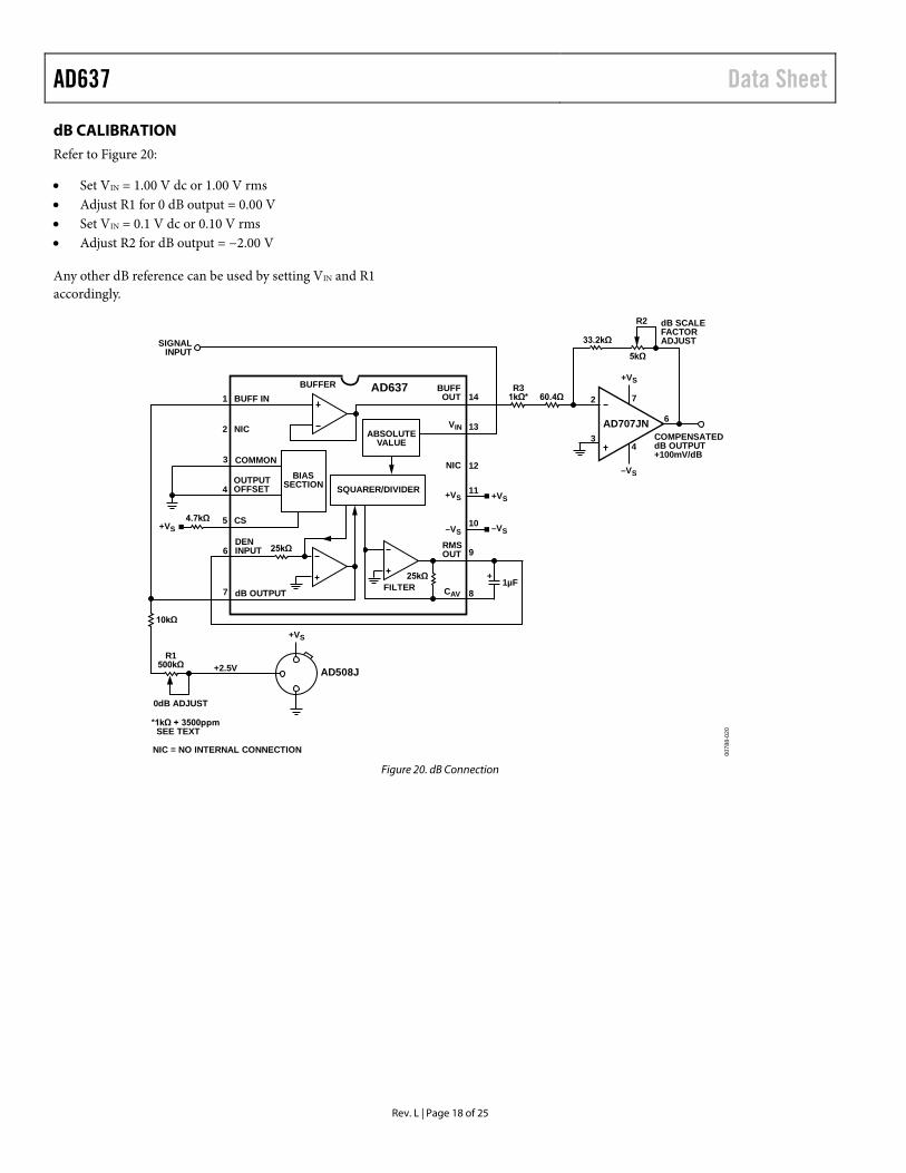
AD637 Data Sheet
dB CALIBRATION Refer to Figure 20:
• Set VIN = 1.00 V dc or 1.00 V rms • Adjust R1 for 0 dB output = 0.00 V • Set VIN = 0.1 V dc or 0.10 V rms • Adjust R2 for dB output = −2.00 V
Any other dB reference can be used by setting VIN and R1 accordingly.
25kΩ
25kΩ
COMMON
OUTPUTOFFSET
DENINPUT
dB OUTPUT
–VS
+VS
NIC
+VS
AD508J+2.5VR1
500kΩ
10kΩ
0078
8-02
0
4.7kΩ+VS –VS
+VS
COMPENSATEDdB OUTPUT+100mV/dB
BIASSECTION
0dB ADJUST
*1kΩ + 3500ppm SEE TEXT
AD707JN
+VS
R2
5kΩ
33.2kΩ
R31kΩ*
BUFFER AD637
FILTER
1
2
3
4
5
6
7
14
13
12
11
10
9
8CAV
+
BUFFOUTBUFF IN
NIC
CS
VIN
1µF
SIGNALINPUT
dB SCALEFACTORADJUST
–VS
60.4Ω 2
34
6
7
ABSOLUTEVALUE
SQUARER/DIVIDER
NIC = NO INTERNAL CONNECTION
RMSOUT
Figure 20. dB Connection
Rev. L | Page 18 of 25
Data Sheet AD637
0078
8-02
1NOTES1. VALUES CHOSEN TO GIVE 0.1% AVERAGING ERROR AT 1Hz.2. NIC = NO INTERNAL CONNECTION.
BUFFER AD637
SQUARER/DIVIDER
BIASSECTION
25kΩ
1
2
3
4
5
6
7
14
13
12
11
10
9
8CAV
+
ABSOLUTEVALUE
NIC SIGNALINPUT
NIC
AD548JNFILTERED
V RMS OUTPUT
1µF
1000pF
6.8MΩ
1MΩ
R
V RMS
4.7kΩ
BUFFOUT
COMMON
OUTPUTOFFSET
BUFF IN
CS
DENINPUT
dB OUTPUT
VIN
RMSOUT
–VS
+VS
CAV13.3µF
499kΩ 1%
VIN2
–VS
+VS
100µF
V–
3
24
7
6
V+
3.3MΩ3.3MΩ
1µF
+VS
+VS
–VS
50kΩOUTPUTOFFSETADJUST
25kΩ
Figure 21. AD637 as a Low Frequency RMS Converter
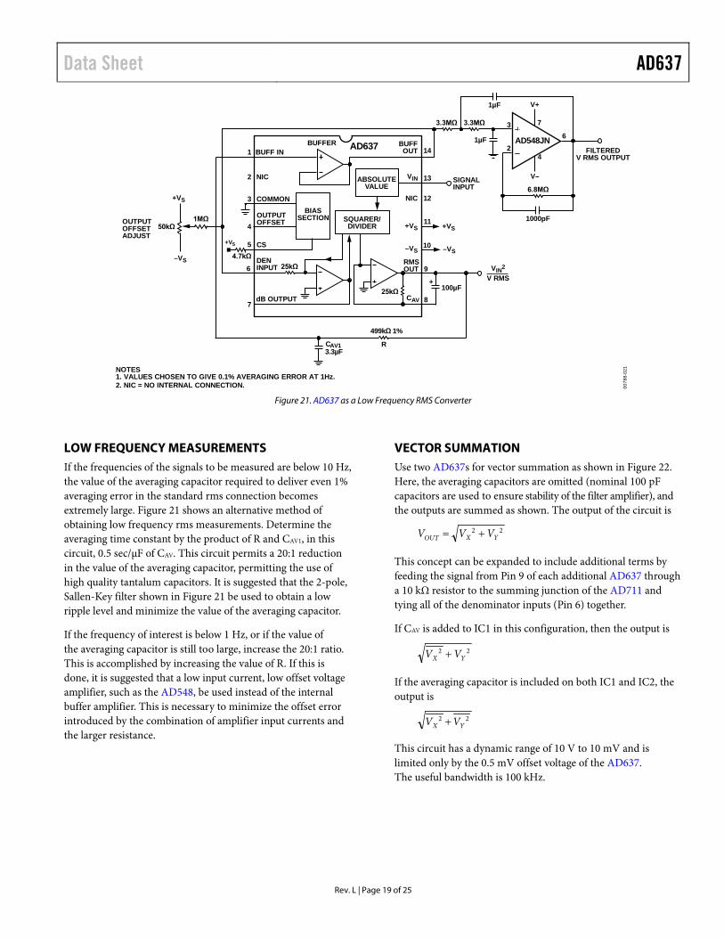
LOW FREQUENCY MEASUREMENTS If the frequencies of the signals to be measured are below 10 Hz, the value of the averaging capacitor required to deliver even 1% averaging error in the standard rms connection becomes extremely large. Figure 21 shows an alternative method of obtaining low frequency rms measurements. Determine the averaging time constant by the product of R and CAV1, in this circuit, 0.5 sec/µF of CAV. This circuit permits a 20:1 reduction in the value of the averaging capacitor, permitting the use of high quality tantalum capacitors. It is suggested that the 2-pole, Sallen-Key filter shown in Figure 21 be used to obtain a low ripple level and minimize the value of the averaging capacitor.
If the frequency of interest is below 1 Hz, or if the value of the averaging capacitor is still too large, increase the 20:1 ratio. This is accomplished by increasing the value of R. If this is done, it is suggested that a low input current, low offset voltage amplifier, such as the AD548, be used instead of the internal buffer amplifier. This is necessary to minimize the offset error introduced by the combination of amplifier input currents and the larger resistance.
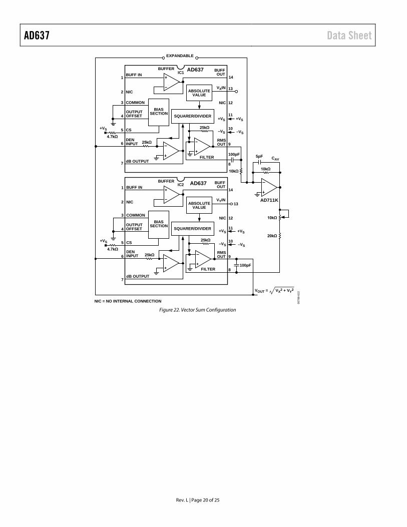
VECTOR SUMMATION Use two AD637s for vector summation as shown in Figure 22. Here, the averaging capacitors are omitted (nominal 100 pF capacitors are used to ensure stability of the filter amplifier), and the outputs are summed as shown. The output of the circuit is
22YXOUT VVV +=
This concept can be expanded to include additional terms by feeding the signal from Pin 9 of each additional AD637 through a 10 kΩ resistor to the summing junction of the AD711 and tying all of the denominator inputs (Pin 6) together.
If CAV is added to IC1 in this configuration, then the output is
22YX VV +
If the averaging capacitor is included on both IC1 and IC2, the output is
22YX VV +
This circuit has a dynamic range of 10 V to 10 mV and is limited only by the 0.5 mV offset voltage of the AD637. The useful bandwidth is 100 kHz.
Rev. L | Page 19 of 25
AD637 Data Sheet
BUFFER AD637
SQUARER/DIVIDERBIAS
SECTION
FILTER
1
2
3
4
5
6
7
14
13
12
11
10
9
ABSOLUTEVALUE
100pF
VXIN
BUFFER AD637
SQUARER/DIVIDER
FILTER
25kΩ
25kΩ
1
2
3
4
5
6
7
14
13
12
11
10
9
8
ABSOLUTEVALUE
100pF
VYIN
5pF
10kΩ
AD711K
EXPANDABLE
10kΩ
10kΩ
IC1
IC2
0078
8-02
2
CAV
BUFFOUT
COMMON
OUTPUTOFFSET
BUFF IN
NIC
CS
DENINPUT
dB OUTPUT
NIC
4.7kΩ
+VS
COMMON
OUTPUTOFFSET
BUFF IN
NIC
CS
DENINPUT
dB OUTPUT
4.7kΩ
+VS
BUFFOUT
NIC
8
–VS –VS
–VS
+VS
BIASSECTION
VX2 + VY2VOUT =
–VS
+VS20kΩ
+VS+VS
25kΩ
25kΩ
NIC = NO INTERNAL CONNECTION
RMSOUT
RMSOUT
Figure 22. Vector Sum Configuration
Rev. L | Page 20 of 25
Data Sheet AD637
Rev. L | Page 21 of 25
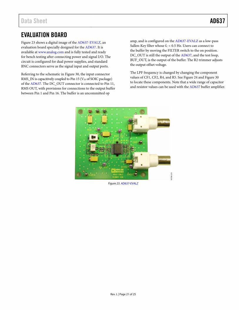
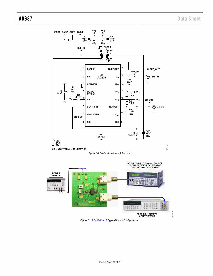
EVALUATION BOARD Figure 23 shows a digital image of the AD637-EVALZ, an evaluation board specially designed for the AD637. It is available at www.analog.com and is fully tested and ready for bench testing after connecting power and signal I/O. The circuit is configured for dual power supplies, and standard BNC connectors serve as the signal input and output ports.
Referring to the schematic in Figure 30, the input connector RMS_IN is capacitively coupled to Pin 15 (VIN of SOIC package) of the AD637. The DC_OUT connector is connected to Pin 11, RMS OUT, with provisions for connections to the output buffer between Pin 1 and Pin 16. The buffer is an uncommitted op
amp, and is configured on the AD637-EVALZ as a low-pass Sallen-Key filter whose fC < 0.5 Hz. Users can connect to the buffer by moving the FILTER switch to the on position. DC_OUT is still the output of the AD637, and the test loop, BUF_OUT, is the output of the buffer. The R2 trimmer adjusts the output offset voltage.
The LPF frequency is changed by changing the component values of CF1, CF2, R4, and R5. See Figure 24 and Figure 30 to locate these components. Note that a wide range of capacitor and resistor values can be used with the AD637 buffer amplifier.
0078
8-12
3
Figure 23. AD637-EVALZ
AD637 Data Sheet
Rev. L | Page 22 of 25
0078
8-12
4
Figure 24. AD637-EVALZ Assembly
0078
8-12
5
Figure 25. Component Side Silkscreen
0078
8-12
6
Figure 26. Evaluation Board—Component Side Copper
0078
8-12
7
Figure 27. Evaluation Board—Secondary Side Copper
0078
8-12
8
Figure 28. Evaluation Board—Internal Power Plane
0078
8-12
9
Figure 29. Evaluation Board—Internal Ground Plane
AD637 Data Sheet
Rev. L | Page 23 of 25
0078
8-13
0
GND1 GND2 GND3 GND4
C110µF25V
C210µF25V
–VS
+
+VS
–VS +VS
+
+
CF247µF25V
CAV22µF16V
+ CF147µF25V
+
+
C30.1µF
CIN22µF16V
BUF_OUT
DC_OUT
RMS_IN
DC_OUT
2
1
4
3
6
5
8
7
15
16
13
14
11
12
9
10
NIC
BUFF IN
OUTPUTOFFSET
COMMON
DEN INPUT
CS
NIC
Z1AD637
dB OUTPUT
VIN
BUFF OUT
+VS
NIC
RMS OUT
–VS
NIC
CAV
R34.7kΩ
+VS
C40.1µF
–VS
R424.3kΩ
R11MΩ
R250kΩ
DB_OUT
BUF_IN
RMS_IN
R524.3kΩ
+VS
+VS–VS
41
2
3
5
6IN
OUT
FILTER
NIC = NO INTERNAL CONNECTION Figure 30. Evaluation Board Schematic
0078
8-13
1
PRECISION DMM TOMONITOR VOUT
POWERSUPPLY
AC OR DC INPUT SIGNAL SOURCEFROM PRECISION CALIBRATOR
OR FUNCTION GENERATOR
Figure 31. AD637-EVALZ Typical Bench Configuration
AD637 Data Sheet
Rev. L | Page 24 of 25
OUTLINE DIMENSIONS
CONTROLLING DIMENSIONS ARE IN INCHES; MILLIMETER DIMENSIONS(IN PARENTHESES) ARE ROUNDED-OFF INCH EQUIVALENTS FORREFERENCE ONLY AND ARE NOT APPROPRIATE FOR USE IN DESIGN
14
1 7
80.310 (7.87)0.220 (5.59)
PIN 1
0.080 (2.03) MAX0.005 (0.13) MIN
SEATINGPLANE
0.023 (0.58)0.014 (0.36)
0.060 (1.52)0.015 (0.38)
0.200 (5.08)MAX
0.200 (5.08)0.125 (3.18) 0.070 (1.78)
0.030 (0.76)
0.100 (2.54)BSC
0.150(3.81)MIN
0.765 (19.43) MAX0.320 (8.13)0.290 (7.37)
0.015 (0.38)0.008 (0.20)
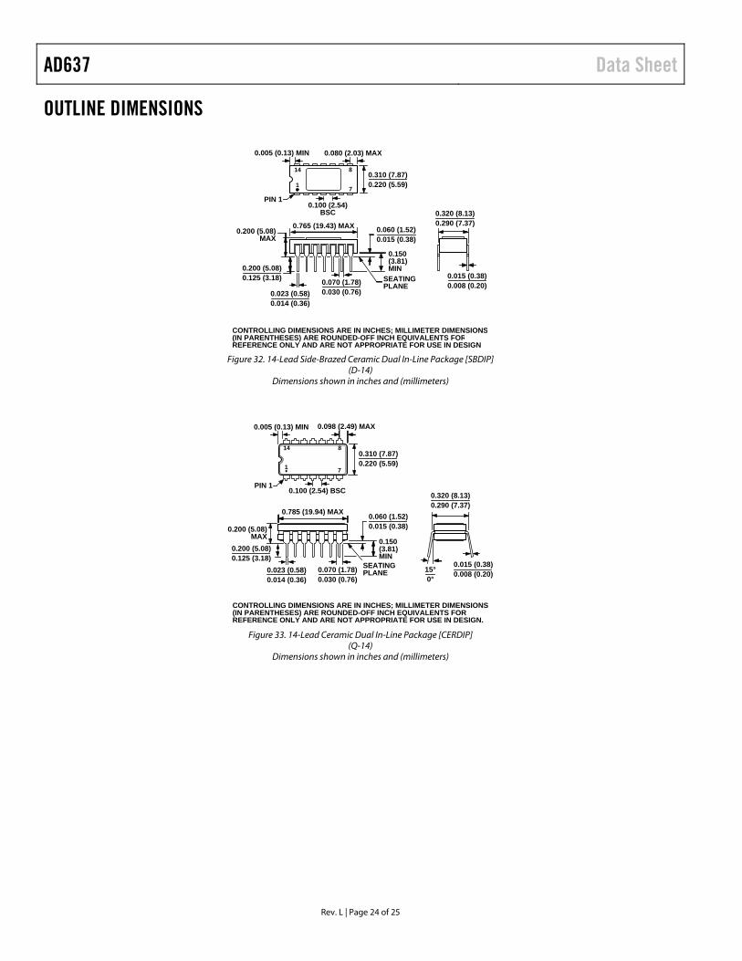
Figure 32. 14-Lead Side-Brazed Ceramic Dual In-Line Package [SBDIP]
(D-14) Dimensions shown in inches and (millimeters)
CONTROLLING DIMENSIONS ARE IN INCHES; MILLIMETER DIMENSIONS(IN PARENTHESES) ARE ROUNDED-OFF INCH EQUIVALENTS FORREFERENCE ONLY AND ARE NOT APPROPRIATE FOR USE IN DESIGN.
0.310 (7.87)0.220 (5.59)
0.005 (0.13) MIN 0.098 (2.49) MAX
0.100 (2.54) BSC
15°0°
0.320 (8.13)0.290 (7.37)
0.015 (0.38)0.008 (0.20)
SEATINGPLANE
0.200 (5.08)MAX
0.785 (19.94) MAX
0.150(3.81)MIN
0.200 (5.08)0.125 (3.18)
0.023 (0.58)0.014 (0.36)
0.070 (1.78)0.030 (0.76)
0.060 (1.52)0.015 (0.38)
PIN 1
1 7
814
Figure 33. 14-Lead Ceramic Dual In-Line Package [CERDIP]
(Q-14) Dimensions shown in inches and (millimeters)
Data Sheet AD637
Rev. L | Page 25 of 25
CONTROLLING DIMENSIONS ARE IN MILLIMETERS; INCH DIMENSIONS(IN PARENTHESES) ARE ROUNDED-OFF MILLIMETER EQUIVALENTS FORREFERENCE ONLY AND ARE NOT APPROPRIATE FOR USE IN DESIGN.
COMPLIANT TO JEDEC STANDARDS MS-013-AA
10.50 (0.4134)10.10 (0.3976)
0.30 (0.0118)0.10 (0.0039)
2.65 (0.1043)2.35 (0.0925)
10.65 (0.4193)10.00 (0.3937)
7.60 (0.2992)7.40 (0.2913)
0.75 (0.0295)0.25 (0.0098) 45°
1.27 (0.0500)0.40 (0.0157)
COPLANARITY0.10 0.33 (0.0130)
0.20 (0.0079)0.51 (0.0201)0.31 (0.0122)
SEATINGPLANE
8°0°
16 9
81
1.27 (0.0500)BSC
03-2
7-20
07-B
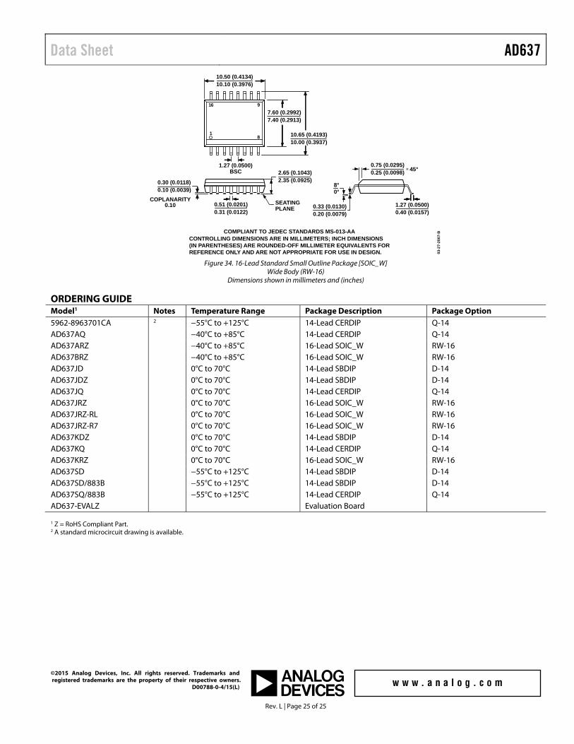
Figure 34. 16-Lead Standard Small Outline Package [SOIC_W]
Wide Body (RW-16) Dimensions shown in millimeters and (inches)
ORDERING GUIDE Model1 Notes Temperature Range Package Description Package Option 5962-8963701CA 2 −55°C to +125°C 14-Lead CERDIP Q-14 AD637AQ −40°C to +85°C 14-Lead CERDIP Q-14 AD637ARZ −40°C to +85°C 16-Lead SOIC_W RW-16 AD637BRZ −40°C to +85°C 16-Lead SOIC_W RW-16 AD637JD 0°C to 70°C 14-Lead SBDIP D-14 AD637JDZ 0°C to 70°C 14-Lead SBDIP D-14 AD637JQ 0°C to 70°C 14-Lead CERDIP Q-14 AD637JRZ 0°C to 70°C 16-Lead SOIC_W RW-16 AD637JRZ-RL 0°C to 70°C 16-Lead SOIC_W RW-16 AD637JRZ-R7 0°C to 70°C 16-Lead SOIC_W RW-16 AD637KDZ 0°C to 70°C 14-Lead SBDIP D-14 AD637KQ 0°C to 70°C 14-Lead CERDIP Q-14 AD637KRZ 0°C to 70°C 16-Lead SOIC_W RW-16 AD637SD −55°C to +125°C 14-Lead SBDIP D-14 AD637SD/883B −55°C to +125°C 14-Lead SBDIP D-14 AD637SQ/883B −55°C to +125°C 14-Lead CERDIP Q-14 AD637-EVALZ Evaluation Board 1 Z = RoHS Compliant Part. 2 A standard microcircuit drawing is available.
©2015 Analog Devices, Inc. All rights reserved. Trademarks and registered trademarks are the property of their respective owners. D00788-0-4/15(L)