high power stepper motor driver mounting the l6480
TRANSCRIPT

This is information on a product in full production. For further information contact your local STMicroelectronics sales office.
September 2012 Doc ID 023675 Rev 1 1/12
12
EVAL6480H
High power stepper motor driver mounting the L6480
Data brief
Features Voltage range from 10.5 V to 85 V
Low Rds(ON) MOSFETs in DPAK package
SPI with daisy chain feature
FLAG and BUSY LED indicators
Adjustable supply voltage compensation
Flexible supply voltage management
Suitable for use in combination with the STEVAL-PCC009V2
Applications High power bipolar stepper motor driving
DescriptionThe EVAL6480H demonstration board is a high power microstepping motor driver. In combination with the STEVAL-PCC009V2 communication board and the evaluation software, the board allows the user to investigate all the features of the L6480 device. In particular, the board can be used to check the voltage mode driving and to regulate the L6480 parameters in order to fit the application requirements.
The EVAL6480H supports the daisy chain configuration making it suitable for the evaluation of the L6480 in multi-motor applications.
www.st.com

Board description EVAL6480H
2/12 Doc ID 023675 Rev 1
1 Board description
Figure 1. Jumper and connector location
Table 1. EVAL6480H electrical specifications
Parameter Value
Supply voltage (VS) 10.5 to 85 V
Maximum output current (each phase) 25 Ar.m.s. at 25 °C(1)
1. Refer to STD25F10 datasheet for details.
External MOSFET Rds(ON) 33 mΩ typical at 25 °C(1)
Gate driver supply voltage (VCC) 7.5 V to 15 V
Logic supply voltage 3.3 V
Logic interface supply voltage 3.3 V or 5 V
Low level logic inputs 0 V
High level logic input VDD(2)
2. All logic inputs are 5 V tolerant.
Operating temperature -25 °C to +125 °C
FLAG LED
Supply managementjumpers
Phase Aconnector
Phase Bconnector
Master SPIconnector
Applicationarea
Slave SPIconnector
External switch connector (SW input)
Motor supply voltagecompensation regulation
(ADCIN input)
Power supply connector(10.5 V - 85 V)
Supply managementconnector
(VS, VSREG, VCCREG and GND)
BUSY LED
AM14874v1
EVAL6480H Board description
Doc ID 023675 Rev 1 3/12
Table 2. Jumper and connector description
Name Type Function
J5 Power supply Main supply voltage
J7 Power output Power bridge A outputs
J8 Power output Power bridge B outputs
J6 Power supply Integrated voltage regulator inputs
J3 SPI Master SPI connector
J4 SPI Slave SPI connector
JP1 Jumper VS to VSREG jumper
JP2 Jumper VSREG to VCC jumper
JP3 Jumper VCC to VCCREG jumper
JP4 Jumper VCCREG to VREG jumper
JP5 Jumper VREG to VDD jumper
JP6 Jumper VDD to 3.3 V from SPI connector jump
JP7 Jumper Daisy chain termination jumper
JP8 Jumper STBY to VS pull-up jumper
TP8 (BUSY/SYNC) Jumper BUSY/SYNC output test point
Table 3. Master SPI connector pinout (J3)
Pin number Type Description
1 Open drain output L6480 BUSY output
2 Open drain output L6480 FLAG output
3 Ground Ground
4 Supply EXT_VDD (can be used as external logic power supply)
5 Digital outputSPI master IN slave OUT signal (connected to the L6480 SDO output through daisy chain termination jumper JP7)
6 Digital input SPI serial clock signal (connected to L6480 CK input)
7 Digital inputSPI master Out slave IN signal (connected to L6480 SDI input)
8 Digital input SPI slave select signal (connected to L6480 CS input)
9 Digital input L6480 step-clock input
10 Digital input L6480 standby/reset input
Table 4. Slave SPI connector pinout (J4)
Pin number Type Description
1 Open drain output L6480 BUSY output
2 Open drain output L6480 FLAG output

Board description EVAL6480H
4/12 Doc ID 023675 Rev 1
3 Ground Ground
4 Supply EXT_VDD (can be used as external logic power supply)
5 Digital outputSPI master In slave Out signal (connected to pin 5 of
J3)
6 Digital input SPI serial clock signal (connected to L6480 CK input)
7 Digital inputSPI master Out slave In signal (connected to L6480 SDO output)
8 Digital input SPI slave select signal (connected to L6480 CS input)
9 Digital input L6480 step-clock input
10 Digital input L6480 standby/reset input
Table 4. Slave SPI connector pinout (J4) (continued)
Pin number Type Description

EVAL6480H Board description
Doc ID 023675 Rev 1 5/12
Figure 2. EVAL6480H schematic part 1/2
SP
I_IN
SP
I_O
UT
App
licat
ion
refe
renc
e
OS
CIN
OS
CO
UT
ST
CK
nCS
CK
SD
IS
DO
BU
SY
F LA
G
nCS
CK
SD
I
BU
SY
BU
SY
FLA
G
FLA
G
nCS
CK
SD
O
ST
BY
_RE
SE
T
ST
BY
_RE
SE
TST
CK
ST
CK
FLA
G
BU
SY
AD
C_
IN
STBY
_RE
SE
T
BU
SY
ST
BY
_RE
SE
T
FLA
G
ST
CK
AD
C_I
N
G_H
S_A
1
G_L
S_A
1
G_H
S_A
2
G_L
S_A
2
G_H
S_B
1
G_H
S_B
2
G_L
S_B
2
G_L
S_B
1
OU
TA
1
OU
TA
2
OU
TB
1
OU
TB
2
ST
BY
AD
C_
IN
VS
VS
_RE
GV
CC
VC
C_R
EG
VR
EG
VD
D
3V3
3V3
VD
DV
DD
VD
DV
DD
3V3
VS
VS
_RE
GV
CC
VC
C_R
EG
VR
EG
VD
D
AD
CIN
1C
522
u/6
V3
JP1
12
VC
C
1
ST
BY
1
U1
L648
0
G_L
S_A
11
OU
T _A
12
G_H
S_A
13
G_L
S_A
238
OU
T_A
237
G_H
S_A
23 6
OU
T_B
118
G_L
S_B
119
OU
T_B
221
G_L
S_B
220
G_H
S_B
117
G_H
S_B
222
PGN
D
2 3
PGN
D
35
AGN
D
16
DG
ND
2 9
V S
6
PGN
D
8
VS
_RE
G12
VCC
10
VC
C_R
EG
11
VR
EG
13
VBO
OT
7
CP9
AD
C_IN
5V
DD
27
STB
Y _R
ES
34
CS
24
SDO
28C
K2 5
SD
I26
OS
C_IN
1 4
OS
C_O
UT
15
SW
33ST C
K32
BU
SY_S
YNC
30
FLA
G31
GN
D
39
N.C
.4
GN
D1
JP3
12
C9
47n
/100
V
C2
220
n/10
0V
JP2
12
J 2 N.M
.1 2 JP7
12
R4 470
C8
100
n/10
0V
C1
470
n/2
5V
J 1 N.M
.1 2
VD
D
1
VS
1
R1
100
C13
10n
/ 6V
3
JP5
12
VR
EG
1
R3
39k
BU
SY
1
C12
100p
/ 6V
3
C7
470n
/ 25V
J31
23
45
67
89
10
J41
23
45
67
89
1 0
JP4
12
JP6
12
C6
100
n/ 2
5V
ST
CK
1
C10
10n
/6V3
R2 39
k
D1
BA
V9
12
3
DL1
LED
- A
MB
ER
2 1
R5
470
C4
100
n/4V
C3
100
n/6V
3
DL2
LED
- RE
D
2 1
FLA
G1
AM14875v1
Board description EVAL6480H
6/12 Doc ID 023675 Rev 1
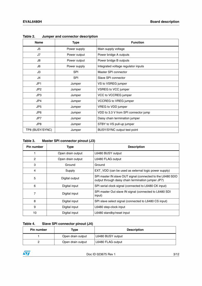
Figure 3. EVAL6480H schematic part 2/2
OP
TIO
N
VS
VS
_RE
GV
CC
_RE
GG
ND
OU
TA
12
OU
TB
12
GN
DVS
App
licat
ion
refe
renc
e
G_H
S_B
2
G_L
S_B
2
G_H
S_B
1
G_L
S_B
1
G_H
S_A
1
G_L
S_A
1
G_H
S_A
2
G_L
S_A
2
OU
TA1
OU
TA2
OU
TB1
OU
TB
2
ST
BY
AD
C_I
N
VSV
SV
S_R
EG
VC
C_R
EG
VS
VS
VS
_RE
GV
SV
DD
VS
VS
JP8
12
Q1
S TD
25N
F10
1
4 3
Q4
STD
25N
F10
1
4
3
C15
220
n/1
00V
D2
BZX5
85- B
3V3
Q5
STD
25N
F10
1
4 3
J8
12
+C
11A
220u
/100
V
Q8
ST
D25
NF
101
4 3
Q2
STD
25N
F10
1
43
C14
220n
/ 100
V
J 6 N.M
.
1 2 3 4
R9
N.M
.
+C
1122
0u
/100
V
R7
100
k/0
.125
W
Q6
STD
25N
F 10
1
43
R6
100 k
/ 0.1
25W
J5
12
R8
50k/
0.125
W
13
2
Q3
STD
25N
F10
1
4 3
J7
12
Q7
ST
D25
NF
101
4 3
D3
BZX5
85- B
3V6
AM14880v1
EVAL6480H Board description
Doc ID 023675 Rev 1 7/12
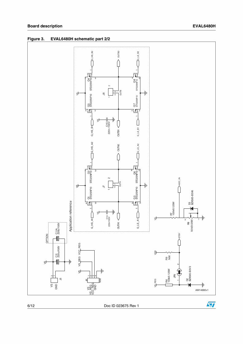
Table 5. EVAL6480H - bill of material
Item Quantity Reference Value Package
1 9
VS, VREG, VDD, VCC,STCK, STBY, FLAG,
BUSY,ADCIN
TPTH-RING-1MM (red) TPTH-RING-1MM
2 2 C1,C7 470 nF/25 V CAPC-0603
3 1 C2 220 nF/100 V CAPC-0805
4 1 C3 100 nF/6.3 V CAPC-0603
5 1 C4 100 nF/4 V CAPC-0603
6 1 C5 22 µF/6.3 V CAPC-1206
7 1 C6 100 nF/25 V CAPC-0603
8 1 C8 100 nF/100 V CAPC-0603
9 1 C9 47 nF/100 V CAPC-0805
10 2 C10, C13 10 nF/6.3 V CAPC-0603
11 1 C11 220 µF/100 V CAPES-R18H17
12 1 C11A 220 µF/100 V CAPE-R16H21-P75
13 1 C12 100 pF/6.3 V CAPC-0603
14 1 DL1 LED amber LEDC-0805
15 1 DL2 LED red LEDC-0805
16 1 D1 BAV99 SOT-23
17 1 D2 BZX585-B3V3 SOD523
18 1 D3 BZX585-B3V6 SOD523
19 1 GND TPTH-RING-1MM (black) TPTH-RING-1MM
20 5 JP1, JP3, JP5, JP7, JP8 Jumper CLOSED JP2SO
21 3 JP2, JP4, JP6 Jumper OPEN JP2SO
22 2 J1, J2 N.M. STRIP254P-M-2
23 1 J3Pol. IDC male header vertical
10 poles (black)CON-FLAT-5X2-180M
24 1 J4Pol. IDC male header vertical
10 poles (gray)CON-FLAT-5X2-180M
25 3 J5, J7, J8 Screw connector 2 poles MORSV-508-2P
26 1 J6 N.M. STRIP254P-M-4
27 8Q1, Q2, Q3, Q4, Q5, Q6,
Q7, Q8STD25NF10 DPAK
28 1 R1 100 Ω RESC-0603
29 2 R2, R3 39 kΩ RESC-0603
30 2 R4, R5 470 Ω RESC-0603
Board description EVAL6480H
8/12 Doc ID 023675 Rev 1
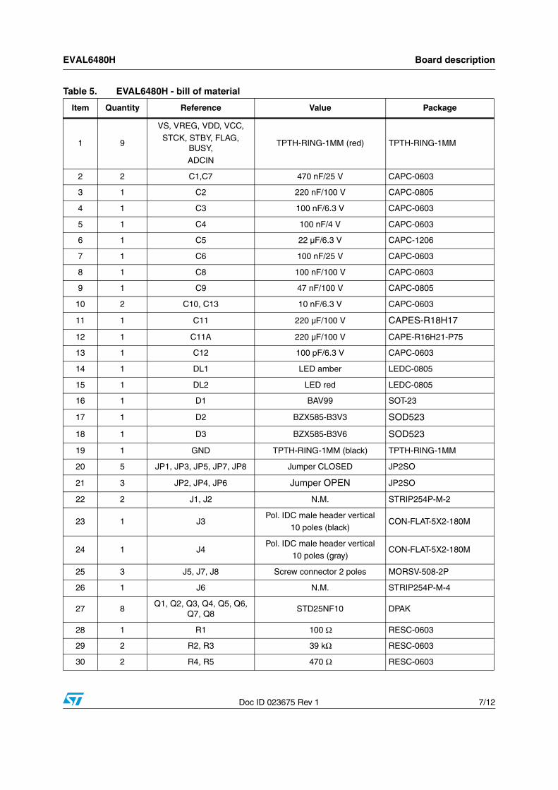
Figure 4. EVAL6480H - layout (top layer)
31 2 R6, R7 100 kΩ / 0.125 W RESC-0603
32 1 R8 33 kΩ / 0.125 WTRIMM-100X50X110-64W
33 1 R9 N.M. RESC-0603
34 1 U1 L6480HTSSOP050P-660X110-38-EP
Table 5. EVAL6480H - bill of material (continued)
Item Quantity Reference Value Package
AM14876v1
EVAL6480H Board description
Doc ID 023675 Rev 1 9/12
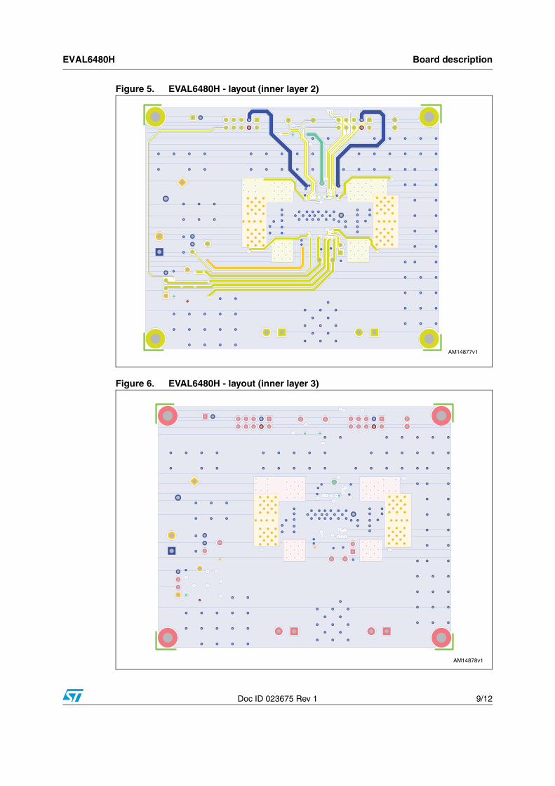
Figure 5. EVAL6480H - layout (inner layer 2)
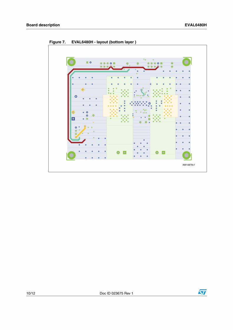
Figure 6. EVAL6480H - layout (inner layer 3)
AM14877v1
AM14878v1
Board description EVAL6480H
10/12 Doc ID 023675 Rev 1
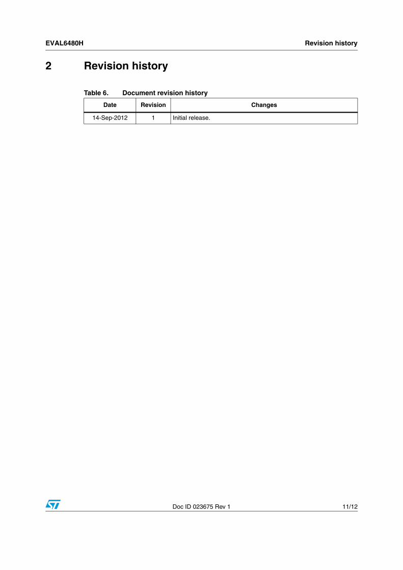
Figure 7. EVAL6480H - layout (bottom layer )
AM14879v1
EVAL6480H Revision history
Doc ID 023675 Rev 1 11/12
2 Revision history
Table 6. Document revision history
Date Revision Changes
14-Sep-2012 1 Initial release.
EVAL6480H
12/12 Doc ID 023675 Rev 1
Please Read Carefully:
Information in this document is provided solely in connection with ST products. STMicroelectronics NV and its subsidiaries (“ST”) reserve theright to make changes, corrections, modifications or improvements, to this document, and the products and services described herein at anytime, without notice.
All ST products are sold pursuant to ST’s terms and conditions of sale.
Purchasers are solely responsible for the choice, selection and use of the ST products and services described herein, and ST assumes noliability whatsoever relating to the choice, selection or use of the ST products and services described herein.
No license, express or implied, by estoppel or otherwise, to any intellectual property rights is granted under this document. If any part of thisdocument refers to any third party products or services it shall not be deemed a license grant by ST for the use of such third party productsor services, or any intellectual property contained therein or considered as a warranty covering the use in any manner whatsoever of suchthird party products or services or any intellectual property contained therein.
UNLESS OTHERWISE SET FORTH IN ST’S TERMS AND CONDITIONS OF SALE ST DISCLAIMS ANY EXPRESS OR IMPLIEDWARRANTY WITH RESPECT TO THE USE AND/OR SALE OF ST PRODUCTS INCLUDING WITHOUT LIMITATION IMPLIEDWARRANTIES OF MERCHANTABILITY, FITNESS FOR A PARTICULAR PURPOSE (AND THEIR EQUIVALENTS UNDER THE LAWSOF ANY JURISDICTION), OR INFRINGEMENT OF ANY PATENT, COPYRIGHT OR OTHER INTELLECTUAL PROPERTY RIGHT.
UNLESS EXPRESSLY APPROVED IN WRITING BY TWO AUTHORIZED ST REPRESENTATIVES, ST PRODUCTS ARE NOTRECOMMENDED, AUTHORIZED OR WARRANTED FOR USE IN MILITARY, AIR CRAFT, SPACE, LIFE SAVING, OR LIFE SUSTAININGAPPLICATIONS, NOR IN PRODUCTS OR SYSTEMS WHERE FAILURE OR MALFUNCTION MAY RESULT IN PERSONAL INJURY,DEATH, OR SEVERE PROPERTY OR ENVIRONMENTAL DAMAGE. ST PRODUCTS WHICH ARE NOT SPECIFIED AS "AUTOMOTIVEGRADE" MAY ONLY BE USED IN AUTOMOTIVE APPLICATIONS AT USER’S OWN RISK.
Resale of ST products with provisions different from the statements and/or technical features set forth in this document shall immediately voidany warranty granted by ST for the ST product or service described herein and shall not create or extend in any manner whatsoever, anyliability of ST.
ST and the ST logo are trademarks or registered trademarks of ST in various countries.
Information in this document supersedes and replaces all information previously supplied.
The ST logo is a registered trademark of STMicroelectronics. All other names are the property of their respective owners.
© 2012 STMicroelectronics - All rights reserved
STMicroelectronics group of companies
Australia - Belgium - Brazil - Canada - China - Czech Republic - Finland - France - Germany - Hong Kong - India - Israel - Italy - Japan - Malaysia - Malta - Morocco - Philippines - Singapore - Spain - Sweden - Switzerland - United Kingdom - United States of America
www.st.com