high performance lcd for augmented reality and virtual
TRANSCRIPT

High performance LCD for augmented reality and virtual reality displaysJaved Rouf Talukder, Yuge Huang and Shin-Tson Wu
College of Optics and Photonics, University of Central Florida, Orlando, FL, USA
ABSTRACTFor augmented reality and virtual reality displays, high-resolution density, high luminance, and fastresponse time are critically needed. High-resolution density helps eliminate the screen-door effect;high luminance and fast response time enable low duty ratio operation, which plays a key role forsuppressing image blurs. By using a low viscosity material and new diamond-shaped electrodeconfiguration, we demonstrate a fringe field switching liquid crystal display, abbreviated as d-FFSLCD, with high transmittance, fast grey-to-grey response time, low operation voltage, wide viewingangle, and indistinguishable colour shift and gamma shift. We also investigate the rubbing angle (α)effects on transmittance and response time. When α = 0°, the virtual wall effect is strong, resultingin fast response time but compromised transmittance. When α ≥ 1.2°, the virtual walls disappear, asa result, the transmittance increases dramatically, but the trade-off is in slower response time.
ARTICLE HISTORYReceived 30 September 2018Accepted 21 October 2018
KEYWORDSLiquid crystals; augmentedreality; virtual reality;displays
1. Introduction
Presently, thin-film-transistor (TFT) liquid crystal dis-play (LCD) and organic light-emitting diode (OLED)displays are two dominating technologies for TVs, smart-phones, and augmented reality (AR) and virtual reality(VR) [1–4]. Although each technology has its own prosand cons [5], a common demand is higher resolutiondensity and fast response time. This is particularly impor-tant for AR and VR displays in order to mitigate theannoying screen door effect. However, as the resolutiondensity increases, the display luminance decreasesbecause of the reduced aperture ratio. Lower opticalefficiency leads to increased power consumption, i.e.shorter battery lifetime for mobile displays. Anotherequally important performance metric is image blur,which is governed by the motion picture response time(MPRT) [6]. MPRT is jointly determined by the TFTframe rate, LCD/OLED response time and duty ratio[7]. Both active matrix LCD and OLED are holding type
displays; thus, they would exhibit different degree ofimage blurs. Under the same frame rate, say 120 Hz, ifan LCD’s response time is below 2 ms, then its MPRT iscomparable to that of OLED, even its response time is asfast as 1 μs. A common approach to suppress the imageblur of LCD and OLED is to lower the duty ratio [7] sothat they behave CRT-like impulse driving. However, tokeep the same luminance, say 150 nits for VR, we have toboost LCD’s backlight brightness or OLED’s driving cur-rent. As a result, efficiency droop in LED backlight [8]takes place or OLED’s lifetime is compromised [9].Therefore, a high transmittance and fast MPRT LCD isurgently needed for the emerging AR and VR displays.
Fringe field switching (FFS) LCD [10] is a favourablechoice for high-resolution density panels because of itsbuilt-in storage capacitor and weak colour shift. The for-mer enables high-resolution density. However, FFS still hassome room for improvement, such as limited contrastratio (CR ~2000:1) and relatively slow response time(10–15 ms due to the small twisted elastic constant K22
CONTACT Shin-Tson Wu [email protected]
LIQUID CRYSTALShttps://doi.org/10.1080/02678292.2018.1540067
© 2018 Informa UK Limited, trading as Taylor & Francis Group

involved). To improve contrast ratio, mini-LED backlightwith area local dimming has been implemented andremarkable result (CR >105:1) has been achieved [11,12].To shorten response time, interdigitated pixel-electrodestructures with two-dimensional standing layers (alsocalled virtual walls) have been proposed [13–16]. Thesevirtual walls exert an additional restoring torque to accel-erate the decay process so that the average grey-to-grey(GTG) response time can be reduced to 3–5 ms. However,a significant trade-off is compromised transmittance dueto the existence of virtual walls.
In this paper, we report a new FFS LCD with dia-mond-shaped electrode structure along with a low-visc-osity LC mixture to simultaneously achieve hightransmittance and fast GTG response time, while preser-ving the inherent advantages on wide-viewing angle andindistinguishable gamma shift and colour shift. Its appli-cation for high-resolution density displays is emphasised.
2. LC material
To obtain high transmittance in a thin cell gap (e.g. 2.5–3.0 μm), we should use a slightly higher birefringence (Δn~0.12) LC material. Meanwhile, a modest dielectric ani-sotropy (Δε = ε//–ε⊥) is required for keeping operationvoltage below 6 V. However, the polar groups contribut-ing to enhance Δε will also lead to an increased viscosity.To achieve high transmittance and fast response time,while keeping low operation voltage, we formulated ahigh Δn LC mixture with balanced dielectric anisotropyand viscosity. Actually, DIC-LC2 (DIC Corp.) exhibits avery low rotational viscosity and relatively high birefrin-gence, except that its dielectric anisotropy is somewhat
too small (Δε ≈ 1.7 at 21°C) [17]. Therefore, to increaseΔε, we mixed 80.9% DIC-LC2 with 19.1% DIC-LC3(Δε ≈ 8.8). For convenience, we call this experimentalmixture as M1. The measured rotational viscosity (γ1),birefringence, dielectric anisotropy, splay elastic constant(K11), twist elastic constant (K22), and activation energy(Ea) are listed in Table 1. Melting temperature (Tm) andclearing temperature (Tc) were measured by DifferentialScanning Calorimetry (DSC, TA instruments Q100).
2.1. Birefringence
Tomeasure the birefringence ofM1, we used a commercialhomogeneous cell with cell gap 7.65 μm. After injectingM1 into a homogeneous cell, we placed the cell on aLinkam heating stage which was controlled by TMS94temperature programmer. We then sandwiched this cellbetween crossed polarisers and applied 1-kHz square-waveAC voltage to this LC cell. A He-Ne laser (λ = 633 nm) wasused as probing beam. Birefringence was calculated fromthe measured phase retardation. Figure 1(a) depicts thetemperature-dependent birefringence at λ = 633 nm,where dots are measured data and solid red line is fittingwith Haller’s semi-empirical equation [18]:
Δn ¼ Δn0S ¼ Δn0 1� T=Tcð Þβ: (1)
In Equation (1), T is the Kelvin temperature, Tc is theclearing point of LC,Δn0 is the extrapolated birefringenceat T = 0, S is the order parameter and β is a materialconstant. From fittings, we obtained Δn0 = 0.1681 andβ = 0.1851 for M1.
Next, we measured the wavelength dispersion of M1by using a He-Ne laser (λ = 633 nm) and a tunable
Table 1. Measured physical properties of M1 at T = 25°C and f = 1 kHz.
LC mixture Δn @ λ = 550 nm ε// ε⊥ Δε γ1 (mPa· s)K11(pN)
K22(pN)
Tm(°C)
Tc(°C)
Ea(meV)
M1 0.1225 5.53 2.87 2.66 35.75 9.93 6.03 –34.5 76.7 248.1
Figure 1. (a) Temperature-dependent Δn of M1 at λ = 633 nm. (b) Δn dispersion of M1 at 25°C. Dots are measured data, and the redlines in (a) and (b) are fitting curves with Equations (1) and (2), respectively.
2 J. R. TALUKDER ET AL.

argon ion laser (λ = 457, 488 and 514 nm). Results areplotted in Figure 1(b), where dots are measured resultsand solid line is the fitting curve with single-bandbirefringence dispersion equation [19]:
Δn ¼ Gλ2λ�2
λ2 � λ�2; (2)
In Equation (2), G is the proportionality constant andλ* is the mean resonance wavelength. Through fittings,we obtained G = 1.740 µm−2 and λ* = 0.239 µm. Usingthese parameters and Equation (2), we find Δn = 0.138,0.123, 0.115 at λ = 450, 550, 650 nm, respectively. Later,we will use these data in our device simulation.
2.2. Visco-elastic coefficient
To determine the visco-elastic coefficient, we measuredthe transient decay time of M1 in a homogeneous cell.Results are shown in Figure 2, where dots are experi-mental data and solid line represents the fitting withfollowing equation [20]:
γ1K11
¼ Aexp Ea=kBTð Þ1� T=Tcð Þβ
: (3)
In Equation (3), A is the proportionality constant, kB isthe Boltzmann constant and Ea is the activation energy.From fittings, we obtained Ea = 248.1 meV. FromFigure 2, we find γ1/K11 = 3.60 ms/μm2 at T = 25°C.Through threshold voltage measurement (not shownhere), we found K11 = 9.93 pN, and subsequentlyγ1 = 35.75 mPas at 25°C.
In order to obtain K22, we filled M1 into a commer-cial IPS (in-plane switching) cell with 3-µm cell gapand measured its transient decay time [21]. From thedecay time constant, we extracted γ1/K22 = 5.93 ms/μm2 at 25°C. From the already obtained γ1, we cancalculate the twist elastic coefficient and result isK22 = 6.03 pN. We will use these parameters in ourdevice simulations discussed below.
3. Device structure
We propose a new device structure to achieve hightransmittance using M1. Figure 3(a,b) depicts thecross-sectional and top views of our proposed electrodeconfiguration. The top substrate has a thin surfacealignment layer (not shown), while bottom substratehas a planar common electrode, a passivation layer,diamond-shaped pixel electrodes and a thin surfacealignment layer (not shown). For simplicity, let us callthe structure shown in Figure 3(b) as diamond-shapedFFS mode, abbreviated as d-FFS. The electrode width,electrode gap and electrode tilt angle are denoted as w,g and φ, respectively, and α is the LC alignment direc-tion (rubbing angle) with respect to y axis.
This structure looks similar to traditional stripe struc-ture from cross-sectional view, but it has diamond shapefrom top view. The reason for making it diamond shapeand spatial shift between adjacent pixel electrodes is toincrease the transmittance by reducing the dead zones ontop of pixel electrodes [22]. The LC cell is sandwichedbetween two crossed linear polarisers. The LC directorsare aligned along y-axis and pretilt angle is θp = 0. Incontrast, the requirement of non-zero pretilt angle inconventional structures limits the tolerable deviationdue to rubbing alignment accuracy [23]. Compared toprevious report on the interdigitated pixel electrodes ofFFS mode, our design significantly boosts the transmit-tance by reducing the dead zones on top of electrodewhile maintaining a comparable response time.
4. Simulation results
We simulated the LC directors distribution of d-FFS cellfilled withM1with a commercial LCD simulator TechwizLCD 3D (Sanayi, Korea) and then calculated the electro-optic properties by using the extended 2 × 2 Jones matrixmethod [24]. The parameters employed in the simula-tion, shown in Figure 3(b), are set as follows: LC cell gap2.5 μm, electrode width w = 2.0 µm, electrode gapg = 3.0 µm, pixel length 20 µm, pixel ITO thickness50 nm, passivation layer thickness 150 nm, pretilt angleθp = 0 and electrode tilt angle φ = 88.85°. Anchoringenergy of the alignment layer is assumed to be strong.
Figure 2. Temperature-dependent visco-elastic coefficient ofM1 at λ = 633 nm. Dots are measured data and red linerepresents the fitting curve with Equation (3). The fitting para-meters are listed in Table 1.
LIQUID CRYSTALS 3

The LC parameters used in this calculation are listed inTable 1. The transmission axis of bottom polariser isparallel to the LC alignment direction. To explore thetolerance of LC alignment angle, we conducted simula-tions with two rubbing angles α = 0° and 1.5°; the formerexhibits fast response time due to virtual walls, while thelatter exhibits high transmittance owing to the disappear-ance of virtual walls, as will be explained later.
4.1. VT curves and response time
To examine at which rubbing angle the virtual wallswould disappear, we calculated the response time(rise + decay) and normalised transmittance at differentrubbing angles. Results are plotted in Figure 4. FromFigure 4, the transmittance is the lowest and the responsetime is the fastest when α = 0°, due to the virtual walleffects. These standing layers exert a strong anchoringforce to shorten the LC response time, but the formeddead zones reduce the transmittance significantly. As therubbing angle increases, the virtual wall effects are gra-dually weakening. The onset takes place at α ≈ 1.1°; above
α ≈ 1.2°, the transmittance increases sharply but theresponse time also increases. As α > 1.5°, the transmit-tance starts to decline gradually (due to decreased phaseretardation), while response time remains more or lessunchanged. Therefore, the optimal rubbing angle liesbetween 1.2° and 2.0°.
Figure 5 shows the simulated voltage-dependenttransmittance (VT) curves at α = 0° and α = 1.5°,while keeping the LC pretilt angle at θp = 0. Atα = 0°, the peak transmittance (at 5.8 Vrms) is 54.9%.Although the transmittance is relatively low, this resultis comparable to those reported in [14–16]. Indeed, thisis a general trade-off between response time and trans-mittance. However, the result at α = 1.5° is quiteunexpected. Its peak transmittance reaches ~82.9% at5.4 Vrms. Detailed physical mechanism will be dis-cussed later. The increased peak transmittance is parti-cularly desirable for high-resolution density displays,where both the aperture ratio and the optical efficiencyare decreased. As will be discussed later, low backlightduty-ratio can be applied to shorten the MPRT to
Figure 3. Schematic diagram of the proposed d-FFS structure. (a) Cross-sectional view, and (b) top view. w: electrode width, g:electrode gap, φ: electrode tilt angle and α: LC alignment direction w.r.t. y axis.
0.55
0.60
0.65
0.70
0.75
0.80
0.85
Transmittance Response Time
Rubbing Angle (degree)
Tra
nsm
ittan
ce
6
7
8
9
10
11
Res
pons
e T
ime
(ms)
0 2 4 6 8 10 12
Figure 4. Simulated transmittance and response time of d-FFSat different rubbing angles.
0.0
0.1
0.2
0.3
0.4
0.5
0.6
0.7
0.8
Tra
nsm
ittan
ce
Voltage (V)
α= 0°α= 1.5°
0 1 2 3 4 5 6 7 8
Figure 5. Simulated VT curves of d-FFS at α = 0° and 1.5°,λ = 550 nm.
4 J. R. TALUKDER ET AL.

1.5 ms. However, the trade-off is decreased-displayluminance. Therefore, the high-transmittance d-FFSLCD offers a promising solution for suppressingimage blurs while keeping a relatively high-displayluminance. The latter is particularly important for thebattery-powered mobile-display devices.
Low viscosity is helpful for achieving fast responsetime. As listed in Table 1, M1 exhibits a very lowrotational viscosity (γ1 = 35.75 mPas). Figure 6 showsthe calculated time-dependent transmittance curves ford-FFS at α = 0° and 1.5°. The voltage corresponding topeak transmittance is applied to calculate the rise timeand decay time. Response time is defined as the trans-mittance change between 10% and 90% of the max-imum value.
At α = 0°, the rise time and decay time are calculatedto be 5.59 and 2.95 ms, whereas at α = 1.5° the rise timeand decay time are 5.75 and 4.75 ms, respectively. Atα = 0°, the observed faster decay time results from therestoring force exerted by the virtual walls. In compar-ison, the response time of our d-FFS is faster than that
of the alternating tilt device under the same rubbingangle [23] because of its slightly thinner cell gap. Ourd-FFS at α = 1.5° offers ~85% transmittance (normal-ised to that of two parallel polarisers) and reasonablyfast response time. Such a high transmittance is com-parable to that of a single-domain FFS mode with apositive Δε LC, but the average GTG response time isabout 2x faster [25].
4.2. Electrode structure optimisation
To find the optimal device parameters, we performsimulation with different electrode width and electrodegap for the d-FFS LCD with α = 1.5°. Figure 7(a) showsthe simulated VT curves where electrode width (w)varies from 2.0 to 4.0 µm, while keeping electrodegap (g) at 3.0 µm.
As Figure 7(a) depicts, the peak transmittancedecreases gradually as the electrode width increasesfrom 2.0 to 4.0 µm due to the enlarged dead zone area.However, the on-state voltage only slightly shifts from 5.4to 5.6 V, as it is less sensitive when a small Δε LC isemployed [26]. Figure 7(b) shows the simulated VTcurves where electrode gap varies from 2.0 to 4.0 µmwhile keeping electrode width at 2.0 µm. As the electrodegap increases, transmittance decreases because more LCdirectors at the centre of electrode do not reorient. Wealso find that the response time does not varymuch as theelectrode width and electrode gap change from 2.0 to4.0 µm. For the d-FFS with w = 2.0 μm and g = 2.0 μm,the simulated peak transmittance is 85.2%, rise time≈5.62 ms and decay time ≈4.77 ms at Von = 5.8Vrms.
Table 2 compares the performance of our proposeddevice with two prior LC devices: Device I and Device II.The goal of this analysis is to distinguish the improvementfrommaterial and device structure. For Device I, a positiveΔε LC material and interdigitated pixel electrode structurewith alternative tilt are used [23]. Device II has the same
0 20 40 60 800.0
0.2
0.4
0.6
0.8
1.0
Nor
mal
ized
Tra
nsm
ittan
ce
Time (ms)
α= 0°α= 1.5°
Figure 6. Simulated response time curves of d-FFS at α = 0°and 1.5°.
0.0
0.1
0.2
0.3
0.4
0.5
0.6
0.7
0.8
Tra
nsm
ittan
ce
Voltage (V)
w=2.0 um w=2.5 um w=3.0 um w=3.5 um w=4.0 um
0 1 2 3 4 5 6 7 8 0 1 2 3 4 5 6 7 80.0
0.1
0.2
0.3
0.4
0.5
0.6
0.7
0.8
Tra
smitt
ance
Voltage (V)
g=2.0 um g=2.5 um g=3.0 um g=3.5 um g=4.0 um
(a) (b)
Figure 7. Simulated VT curves of d-FFS using M1. (a) Keeping electrode gap at 3.0 μm while varying electrode width from 2.0 to4.0 µm. (b) Keeping electrode width at 2.0 µm while varying electrode gap from 2.0 to 4.0 µm.
LIQUID CRYSTALS 5

configuration as Device I, except that the employed LCmaterial is replaced by our M1mixture. For a fair compar-ison, we use the same electrode width (2.0 µm), electrodegap (2.0 µm) and cell gap (2.5 µm). While comparingDevice II with Device I, we find that the rise time anddecay time are all reduced for both α = 0°and α = 1.5°. Thisis because M1 has a lower viscosity (35.75 mPas vs.47.6 mPas). Moreover, for the case of α = 1.5°, the trans-mittance of Device II is higher than that of Device I(79.41% vs. 69.52%). The enhanced transmittance is theproduct of smallerΔε [27] and higher ε⊥/ε//ratio [28] of ourM1 mixture. However, a major trade-off is increased on-state voltage because M1 has a smaller Δε (2.66 vs. 5.1) inDevice II. When comparing our proposed device withDevice II (using the same M1 mixture), we find theimprovement is in three areas: (1) the transmittance isimproved from 79.4% to 85.2%, (2) the on-state voltageis decreased from 6.4 to 5.8 V and (3) the response time(rise + decay) is slightly faster (from 11.4 to 10.4 ms). Thelower operation voltage is due to the electrode shape anduniform tilt and twist angles of LC directors in the voltage-on state.
5. Discussion
In order to get high transmittance, fast response time andlow operation voltage, we have introduced an improvedmixture to our d-FFS mode. Our LC material exhibits alow viscosity which helps to reduce response time.However, the trade-off is its low Δε, which leads to
increased operation voltage. With our diamond-shapedelectrodes, we are able to keep a high transmittance(~85%) at 5.8 V. To lower the operating voltage to 5 V(similar to that of most commercial LCDs), we need toincrease Δε by ~35%, which would slightly increase theviscosity. It is worth mentioning that the electric field inour d-FFSmode is at an oblique angle to the LC directors,which eliminates the requirement of non-zero pretiltangle for forming two-domain LC confinement.Figure 8(a,b) shows the cross-sectional view of LC direc-tor configuration and the corresponding transmittance ata voltage-on state for α = 0° and α = 1.5°, respectively. InFigure 8(a), because the rubbing angle is zero, the virtualwalls above the electrodes provide additional restoringforce to the LC directors. Hence, fast response is obtained.However, dead zones are formed at the same time, lead-ing to a relatively low transmittance. To boost transmit-tance, we investigated the device configuration withα = 1.5°. As Figure 8(b) depicts, the LC directors abovethe electrodes are also reoriented by the electric field,which reduces the dead zone area. In addition, the spatialshift between adjacent pixels and common electrodeshelps to spread the electric field more uniformly, whichalso contributes to the increased transmittance. Ourd-FFS with α = 1.5° rubbing angle is very preferable interms of transmittance while the trade-off in responsetime is minimal. In the following sections, we will showthe calculated GTG response time, MPRT, viewing angle,gamma shift and colour shift for our d-FFS at α = 0° andα = 1.5° rubbing angle with optimised structure.
5.1. Grey-to-grey (GTG) response time
We divide the VT curve uniformly into 256 grey levelsbased on gamma-2.2 rule in order to obtain the responsetime between different grey levels. We study the transi-tions between 0, 64, 128, 192 and 255 grey levels. TheGTG response time (rise and decay) is defined between10% and 90% transmittance change. The simulated GTGresponse times are listed in Tables 3 and 4 for α = 0° and
Table 2. Calculated peak transmittance and response time atthe on voltage for three LC devices.
LC DeviceRubbingangle
Voltage(V) Transmittance
Rise(ms)
Decay(ms)
Device I 0° 5.0 47.0% 5.9 3.21.5° 5.2 69.5% 7.0 6.1
Device II 0° 6.6 47.0% 5.2 2.51.5° 6.4 79.4% 6.7 4.7
Proposeddevice
0° 6.2 51.1% 5.0 2.41.5° 5.8 85.2% 5.6 4.8
Figure 8. Cross-sectional view of the simulated LC director distributions and local relative transmittance of d-FFS cell at (a) α = 0°and (b) α = 1.5° rubbing angle.
6 J. R. TALUKDER ET AL.
α = 1.5°, respectively. From Tables 3 and 4, the averageGTG response time is found to be 5.35 ms for α = 0°, and8.81 ms for α = 1.5°. The faster average GTG responsetime for α = 0° is expected because of the virtual walls.However, its transmittance is greatly sacrificed.
To evaluate image blurs of a TFT-LCD or OLED,MPRT should be considered. For a TFT-LCD, itsMPRT depends on the LC response time and TFTframe rate as [7]:
MPRT �ffiffiffiffiffiffiffiffiffiffiffiffiffiffiffiffiffiffiffiffiffiffiffiffiffiffiffiffiffiffiffiffiτ2 þ ð0:8� Tf Þ2
q: (4)
In Equation (4), τ is the LC response time and Tf (= 1000/f) is the TFT frame time. Based on Equation (4), if the FFSdevice is driven at 144 Hz, then its corresponding averageGTG MPRT should be 7.82 and 10.41 ms at α = 0° andα = 1.5°, respectively. Both are too slow and image blurwould be inevitable. To suppress image blurs to unnotice-able level, we set CRT-like MPRT as the criterion, whichis 1.5 ms. From Equation (4), if τ ≈ 5 ms, then it isimpossible to reduce the MPRT to 1.5 ms, even weincrease the frame rate. Another drawback for increasingframe rate is the dramatically shortened TFT chargingtime, especially for a high-resolution (4K2K) display. Amore effective way to reduce MPRT is to decrease theduty ratio [29,30]. Especially, when the duty ratio is low,MPRT is less sensitive to the LC response time. This isbecause the backlight is turned on at a later stage so that
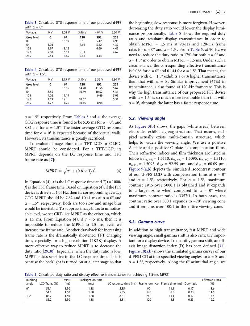
the beginning slow response is more forgiven. However,decreasing the duty ratio would lower the display lumi-nance proportionally. Table 5 shows the required dutyratio and resultant display transmittance in order toobtain MPRT = 1.5 ms at 90-Hz and 120-Hz framerates for α = 0° and α = 1.5°. From Table 5, at 90 Hz weneed to reduce the duty ratio to 17% for both α = 0° andα = 1.5° in order to obtain MPRT = 1.5 ms. Under such acircumstance, the corresponding effective transmittanceis 0.086 for α = 0° and 0.144 for α = 1.5°. That means, thedevice with α = 1.5° exhibits a 67% higher transmittancethan that with α = 0°. Similar improvement (67%) intransmittance is also found at 120-Hz framerate. This iswhy the high transmittance of our proposed FFS devicewith α = 1.5° is so much more favourable than that withα = 0°, although the latter has a faster response time.
5.2. Viewing angle
As Figure 3(b) shows, the gaps (white areas) betweenelectrodes exhibit zig-zag structure. That means, eachpixel actually exists multi-domain structure, whichhelps to widen the viewing angle. We use a positiveA-plate and a positive C-plate as compensation films.Their refractive indices and film thickness are listed asfollows: ne, +A = 1.5110, no, +A = 1.5095, ne, +C = 1.5110,no,+C = 1.5095, d+A = 92.59 µm, and d+C = 60.09 µm.Figure 9(a,b) depicts the simulated isocontrast contourof our d-FFS LCD with compensation films at α = 0°and α = 1.5°, respectively. For α = 1.5°, maximumcontrast ratio over 5000:1 is obtained and it expandsto a larger zone when compared to α = 0° wheremaximum contrast ratio is 3357:1. In both cases, thecontrast ratio over 500:1 expands to ~70° viewing coneand it remains over 100:1 in the entire viewing cone.
5.3. Gamma curve
In addition to high transmittance, fast MPRT and wideviewing angle, small gamma shift is also critically impor-tant for a display device. To quantify gamma shift, an off-axis image distortion index (D) has been defined [31].Figure 10(a,b) shows the simulated gamma curves of ourd-FFS LCD at four specified viewing angles for α = 0° andα = 1.5°, respectively. Along the 0° azimuthal angle, we
Table 3. Calculated GTG response time of our proposed d-FFSwith α = 0°.Voltage 0 V 3.08 V 3.46 V 4.04 V 6.20 V
Grey level 0 64 128 192 2550 13.19 8.5 5.42 4.9564 1.93 7.66 5.12 4.37128 1.97 8.12 4.69 4.49192 2.08 6.12 5.31 4.67255 2.43 5.85 5.68 4.44
Table 4. Calculated GTG response time of our proposed d-FFSwith α = 1.5°.Voltage 0 V 2.75 V 3.10 V 3.55 V 5.80 V
Grey level 0 64 128 192 2550 16.15 14.70 11.56 5.6264 3.85 10.69 10.52 5.31128 4.02 11.19 9.49 5.09192 4.19 12 10.67 5.31255 4.77 11.76 10.45 8.98
Table 5. Calculated duty ratio and display effective transmittance for achieving 1.5-ms MPRT.Rubbingangle LCD Trans. (%)
MPRT(ms)
Backlight on-time(ms) LC response time (ms) Frame rate (Hz) Frame time (ms) Duty ratio
Effective Trans.(%)
0° 51.1 1.50 1.88 5.35 90 11.1 0.17 8.651.1 1.50 1.88 5.35 120 8.3 0.23 11.5
1.5° 85.2 1.50 1.88 8.81 90 11.1 0.17 14.485.2 1.50 1.88 8.81 120 8.3 0.23 19.2
LIQUID CRYSTALS 7

find D(60°, 0°) = 0.182 for α = 0° and D = 0.113 forα = 1.5°. In both scenarios, D is smaller than 0.2, whichmeans the gamma shift of our d-FFS LCD is indistin-guishable by the human eye [32].
5.4. Colour shift
Indistinguishable colour shift is another critical require-ment of all display devices. By using a quantum dotenhancement film [33,34], we calculated the colour shiftof our d-FFS LCD at different viewing angles. Colour
shift in Δu′v′ colour coordinate system at different polarangles (at 0° azimuthal angle) are shown in Figure 11(a,b)at α = 0° and α = 1.5°, respectively. From Figure 11, thecolour difference for RGB wavelengths is smaller than0.008 even at ~ 80° viewing cone. When Δu′v′ is smallerthan 0.02, it is indistinguishable to the human eye.
6. Conclusion
We have reported a positive Δε LC mixture and adiamond-shaped pixel configuration for FFS mode.
Figure 9. Simulated isocontrast contour of d-FFS LCD with (a) α = 0° and (b) α = 1.5° using a positive A-plate and a positive C-plate.
0.0
0.2
0.4
0.6
0.8
1.0
Tra
nsm
ittan
ce
Gray Level
θ = 0°θ = 20°θ = 40°θ = 60°
0.0
0.2
0.4
0.6
0.8
1.0
Tra
nsm
ittan
ce
Gray Level
θ = 0°θ = 20°θ = 40°θ = 60°
0 50 100 150 200 250 0 50 100 150 200 250
(a) (b)
Figure 10. Simulated gamma shift of the film-compensated d-FFS LCD at (a) α = 0° and (b) α = 1.5°.
0.000
0.002
0.004
0.006
0.008
Col
or D
iffer
ence
Δ u' v' (
a.u.
)
Viewing angle (degree)
Red Green Blue
-80 -60 -40 -20 0 20 40 60 80 -80 -60 -40 -20 0 20 40 60 80
0.000
0.002
0.004
0.006
0.008
Col
or D
iffer
ence
Δ u' v' (
a.u.
)
Viewing angle (degree)
Red Green Blue
(a) (b)
Figure 11. Simulated colour shift at (a) α = 0° and (b) α = 1.5° using a quantum dot-enhanced backlight.
8 J. R. TALUKDER ET AL.

High transmittance (Tmax ~85%), fast response time(average GTG ~2.92 ms) and low operation voltage(5.8V) have been achieved. High transmittance andfast LC response time are critical for high-resolutiondensity and high frame rate displays to keep low powerconsumption and to mitigate image blurs. We havealso achieved high contrast ratio, wide view and indis-tinguishable colour shift and gamma shift by usingcompensation films. Considering these outstandingfeatures, our proposed d-FFS LCD should have poten-tial for many practical applications.
Acknowledgments
The authors would like to thank Haiwei Chen, Guanjun Tanand Fangwang Gou for helpful discussion.
Disclosure statement
No potential conflict of interest was reported by the authors.
Funding
This work was funded by Air Force Office of ScientificResearch (AFOSR) (FA9550-14-1-0279).
References
[1] Schadt M. Milestone in the history of field-effect liquidcrystal displays and materials. Jpn J Appl Phys. 2009;48:03B001.
[2] Tsujimura T. OLED display fundamentals and applica-tions. 2nd ed. Chichester (UK): Wiley; 2017.
[3] Hua H. Enabling focus cues in head-mounted displays.Proc IEEE. 2017;105(5):805–824.
[4] Chen H, Gou F, Wu ST. A submillisecond-responsenematic liquid crystal for augmented reality displays.Opt Mater Express. 2017;7(1):195–201.
[5] Chen H, Lee JH, Lin BY, et al. Liquid crystal display andorganic light-emitting diode display: present status andfuture perspectives. Light Sci Appl. 2018;7:17168.
[6] Igarashi Y, Yamamoto T, Tanaka Y, et al. Summary ofmoving picture response time (MPRT) and futures. SIDInt Symp Digest Tech Papers. 2004;35(1):1262–1265.
[7] Peng F, Chen H, Gou F, et al. Analytical equation forthe motion picture response time of display devices. JAppl Phys. 2017;121(2):023108.
[8] Murawski C, Leo K, Gather MC. Efficiency roll-off inorganic light-emitting diodes. Adv Mater. 2013;25:6801–6827.
[9] Féry C, Racine B, Vaufrey D, et al. Physical mechanismresponsible for the stretched exponential decay behaviorof aging organic light-emitting diodes. Appl Phys Lett.2005;87:213502.
[10] Lee SH, Lee SL, Kim HY. Electro-optic characteristicsand switching principle of a nematic liquid crystal cellcontrolled by fringe field switching. Appl Phys Lett.1998;73(20):2881–2883.
[11] Deng Z, Zheng B, Zheng J, et al. High dynamic rangeincell LCD with excellent performance. SID Symp DigTech Papers. 2018;49(1):996–998.
[12] Tan G, Huang Y, Chen MC, et al. High dynamic rangeliquid crystal displays with a mini-LED backlight. OptExpress. 2018;26(13):16572–16584.
[13] JiaoM,GeZ,WuST, et al. Submillisecond response nematicliquid crystalmodulators using dual fringe field switching ina vertically aligned cell. Appl Phys Lett. 2008;92:111101.
[14] Matsushima T, Seki K, Kimura S, et al. New fastresponse in-plane switching liquid crystal mode. J SocInf Disp. 2018;26(10):602–609.
[15] Choi TH, Oh SW, Park YJ, et al. Fast fringe-fieldswitching of a liquid crystal cell by two-dimensionalconfinement with virtual walls. Sci Rep. 2016;6:27936.
[16] Katayama T, Higashida S, KanashimaA, et al. Developmentof in-plane super-fast response (ip-SFR) LCD for VR-HMD. SID Int Symp Digest Tech Papers. 2018;49(1):671–673.
[17] Takatsu H Advanced liquid crystal materials for activematrix displays. Proceedings of the Advanced DisplayMaterials and Devices; 2014 Jul 23–25; Sendai, Japan.
[18] Haller I. Thermodynamic and static properties of liquidcrystals. Prog Solid State Chem. 1975;10(2):103–118.
[19] Wu ST. Birefringence dispersions of liquid crystals.Phys Rev A. 1986;33(2):1270–1274.
[20] Wu ST, Wu CS. Rotational viscosity of nematic liquidcrystals a critical examination of existing models. LiqCryst. 1990;8(2):171–182.
[21] Xu D, Peng F, Tan G, et al. A semi-empirical equationfor the response time of in-plane switching liquid crystaland measurement of twist elastic constant. J Appl Phys.2015;117:203103.
[22] Chen H, Lan YF, Tsai CY, et al. Low-voltage blue-phaseliquid crystal display with diamond-shape electrodes.Liq Cryst. 2017;44(7):1124–1130.
[23] Choi TH, Woo JH, Choi Y, et al. Interdigitated pixel elec-trodes with alternating tilts for fast fringe-field switching ofliquid crystals. Opt Express. 2016;24(24):27569–27576.
[24] Lien A. Extended Jones matrix representation for thetwisted nematic liquid crystal display at oblique inci-dence. Appl Phys Lett. 1990;57(26):2767–2769.
[25] Ge Z, Wu ST, Kim SS, et al. Thin cell fringing-field-switching liquid crystal display with a chiral dopant.Appl Phys Lett. 2008;92:181109.
[26] Chen H, Peng F, Luo Z, et al. High performance liquidcrystal displays with a low dielectric constant material.Opt Mater Express. 2014;4(11):2262–2273.
[27] Ryu JW, Lee JY, Kim HY, et al. Effect of magnitude ofdielectric anisotropy of a liquid crystal on light effi-ciency in the fringe-field switching nematic liquid crys-tal cell. Liq Cryst. 2008;35(4):407–411.
[28] Kang SW, Jang IW,KimDH, et al. Enhancing transmittanceof fringe-field switching liquid crystal device by controllingperpendicular component of dielectric constant of liquidcrystal. Jpn J Appl Phys. 2014;53(1):010304.
LIQUID CRYSTALS 9

[29] Ito H, Ogawa M, Sunaga S. Evaluation of an organic light-emitting diode display for precise visual stimulation. J Vis.2013;13(7):6.
[30] Gou F, Chen H, Li M, et al. Motion-blur-free LCD for highresolution virtual reality displays. J Soc Inf Disp. 2018;26(4):223–228.
[31] Park SB, Song JK, Um Y, et al. Pixel-division technologyfor high-quality vertical-alignment LCDs. IEEE ElectronDevice Lett. 2010;31(9):987–989.
[32] Kim SS, Berkeley BH, Kim KH, et al. New technologies foradvanced LCD-TV performance. J Soc Inf Disp. 2004;12(4):353–359.
[33] Luo Z, Xu D, Wu ST. Emerging quantum-dots-enhanced LCDs. J Disp Technol. 2014;10(7):526–539.
[34] Chen H, He J, Wu ST. Recent advances in quantum-dot-enhanced liquid crystal displays. IEEE J Sel TopicsQuantum Electron. 2017;23(5):1900611.
10 J. R. TALUKDER ET AL.