high-performance computing for the … · nasa-cr-200687 high-performance computing for the...
TRANSCRIPT
,_. NASA-CR-200687
HIGH-PERFORMANCE COMPUTING FOR THE
ELECTROMAGNETIC MODELING AND
SIMULATION OF INTERCONNECTS
Final Report
NASA - FAR Grant NAG 2-823
Jose E. Schutt-Aine
Department of Electrical and Computer Engineering
University of Illinois, Urbana, IL
February 1996J
https://ntrs.nasa.gov/search.jsp?R=19960016735 2018-07-29T21:56:10+00:00Z

SUMMARY
The electromagnetic modeling of packages and interconnects plays a very important
role in the design of high-speed digital circuits, and is most efficiently performed by
using computer-aided design algorithms. In recent years, packaging has become a
critical area in the design of high-speed communication systems and fast computers, and
the importance of the software support for their development has increased accordingly.
Throughout this project, our efforts have focused on the development of modeling and
simulation techniques and algorithms that permit the fast computation of the electrical
parameters of interconnects and the efficient simulation of their electrical performance.

PROJECT DESCRIPTION
The development of efficient and accurate computer-aided design tools is essential
for the implementation of high-speed digital circuits used in computer systems and
communication networks. With current trends in which network complexity and signal
speed keep increasing, problems associated with signal integrity such as crosstalk,
distortion, losses can compromise the overall electrical performance of computers and
communication systems.
Presently, industrial needs for computer support in network design is increasing
rapidly; however the availability of design and analysis tools capable of handling the
complexity and volume of manufactured systems lags seriously. Future winners in the
competitive world of high-speed communications will have to possess sophisticated
packaging analysis and design tools and system performance will be more and more
determined by the adequacy of these tools.
Because of their important role in the design process, CAD tools must offer certain
essential features such as speed, accuracy, availability of extensive library and good user
interface. CAD tools will insure minimum manufacturing cost, faster turnaround time
and more reliable hardware for production. To achieve the required performance,
optimization routines must be made available and efficient algorithms must be
implemented to guarantee speed and good user interface, friendliness and portability of
the software.
Our group at the University of Illinois has been involved during the past three years
in the development of modeling and simulation techniques for interconnects and
packages. In the parent project, the main emphasis of our work is directed toward the
modeling of complex interconnect structures as well as the simulation of interconnects.
The development of efficient and accurate computer-aided design tools is essential
for the implementation of high-speed digital circuits used in computer systems and
communication networks. With increasing clock rates and reduced circuit sizes,
electromagnetic phenomena such as crosstalk noise, distortion, ground bounce will
become more pronounced in both circuit boards and chip environment. These effects
seriously degrade the signal integrity of high-speed networks and compromise the
overall network performance.

Development of Interconnect Modeling Techniques
In many situations, one factor that contributes to the increased computation time in
the calculation of the electrical parameters of the Green's function in the spatial domain,
which represents the vector field produced by an infinitesimal dipole placed over the
dielectric substrate layer backed by a ground plane. An efficient method to compute the
2-D and 3-D capacitance matrix of multiconductor interconnects in a multilayered
dielectric medium was developed in our group. The method is applicable to conductors
of arbitrary polygon shape embedded in a multilayered dielectric medium with possible
ground planes on the top or bottom of the dielectric layers [2], [7]. The method has been
extended to the computation of equivalent capacitance of via structures in multilayer
environment [5].
In the time domain analysis, the ability to model fine features, e.g., wire bonds, is an
important requirement and is unavailable in the conventional finite-difference time-
domain (FDTD) approach unless a very high density of discretization is employed. The
FDTD method is one of the most widely used techniques. In the FDTD, the derivative
operators are replaced with the central difference operators, which preserves the second
order accuracy. Hence, its extension to the general nonuniform grids is not possible
without losing the second order accuracy or reformulating in terms of the curvilinear
coordinates. However, in solving any practical problems nonuniform grids are highly
desirable due to the limitation of computer resources.
An efficient way to implement the surface impedance boundary condition (SIBC) for
the finite-difference time-domain FDTD method was introduced [4]. Surface impedance
boundary conditions are first formulated for a lossy dielectric half-space in the frequency
domain. The impedance function of a lossy medium is approximated with a series of
first-order rational functions. Then the resulting time-domain convolution integrals are
computed using recursive formulas which are obtained by assuming that the fields are
piecewise linear in time. Thus the recursive formulas derived are second-order accurate.
The preprocessing time is eliminated by performing a rational approximation on the
normalized frequency-domain impedance. This approximation is independent of material
properties.

Simulation of Interconnects
In the real world of electronic packaging, transmission lines are more likely to be
nonuniform and may include discontinuities such as bends, tapers and transitions; hence,
the standard simulation tools for uniform lines can no longer be used to analyze them.
Presently, a number of methods are available for the simulation of coupled transmission
lines that are used to model interconnects. In the past two years, we have carried out a
systematic comparison of these methods with a view to developing an approach that
would be optimal in terms of both accuracy and efficiency. This has led to the
development of a transient simulation method based on the difference approximation
which has the highly desirable feature that it can be conveniently incorporated in a
circuit simulator [6]-[7], [10]-[13]. This approach not only outperforms the standard
scattering parameter method, but is very accurate and computationally efficient as well.
Software designers at Cadence Design Systems and Intel have recently implemented this
method in the latest circuit simulators.
The problem of distributed line simulation was analyzed, and the optimal method,
which results in the maximum efficiency, accuracy and practical applicability, was
developed. The method is applicable to transmission lines characterized by frequency or
time-domain data samples. The resulting line model can be directly used in a circuit
'simulator. The efficiency of the optimal method allows for the accurate transient
simulation of real circuits containing thousands of lossy coupled frequency-dependent
nonuniform lines surrounded by nonlinear active devices with virtually no increase in the
simulation time compared to that for the simple replacement of interconnects with
lumped resistors.
As components of the optimal method, the following novel techniques were
introduced:
- The system model for uniform and nonuniform lines which simplifies analysis of
distributed networks; the open-loop device model for uniform and nonuniform lines
which relates voltages and currents at the line terminals via the simplest possible transfer
functions and time-domain responses;
- The indirect numerical integration--a class of numerical integration methods, which has
ideal accuracy, convergence and stability properties;
- The differenceapproximation,a generalmethodfor applying numericalintegrationtosystemscharacterizedby discretedatasampleswasdevelopedandput in amatrix form.
- The matrix delay separation from the matrix propagation function, which avoids the use
of frequency-dependent modal transformation matrices;
- The relaxation interpolation method, which allows for an accurate and efficient
approximation of line responses in the time and frequency domains, automatically
reduces the approximation order depending on the original function and eliminates
spurious positive poles.
The complete set of frequency-domain relationships between the matrix Z, Y and S
parameters were derived and the direct interpolation-based complex rational
approximation method for transient simulation of macromodels for complicated multiport
interconnects (such as IC packages and connectors) was developed. The direct
interpolation-based method was applied to the automatic generation of lumped
equivalent-circuit models of multiport EM systems (with Dan).
Approximation Techniques for Circuit Analysis
Our research has also been focused in developing a unified methodology of model-
order reduction techniques for circuit and interconnects simulation. The following three
classes of model-order reduction methods: moment-matching technique, Krylov subspace
techniques, and reduced optimum approximation have been studied and their applications
for efficient circuit simulations have been identified.
The moment-matching technique has been shown to be very effective for generating
low order models for linear lumped and distributed systems. The method is useful for
systems whose main features can be retained by the first few orders of reduced system
models. These include the response estimations of linear lumped networks of medium
complexity, wave propagation in transmission lines with short delays and diffusion
process in p-n junctions [20].
Krylov subspace based methods such as Arnoldi algorithm and Lanczos algorithm are
effective and robust in generating reduced-order model of large complex systems
described by ordinary differential or difference equations. The methods are important in
obtaining reduced-order models to systems that can be characterized by relatively higher

order models.The methodsavoid theconstructionof ill-conditioned moment matrices
and the loss of information contained by the eigenvalues of the systems with smaller
magnitudes when higher models are sought. The methods are suitable for analyzing large,
complex lumped networks.
An optimum approximation in conjuction with model order reduction techniques such
as balanced representation and aggregation methods represents a very effective
methodology for generating reduced-order models of complex interconnects (infinite
dimension systems). The approximation method is applied to the distributed systems to
drive high-order finite models as an intermediate stage and then using balanced
transformation and aggregation method lower-order models are generated.

Publications
[1] K. S. Oh and Jos6 E. Schutt-Ain6, "Transient Analysis of Coupled TaperedTransmission Lines with Arbitrary Nonlinear Terminations," IEEE Trans. on Microwave
Theory_ Tech., vol. MTT-41, pp. 268-273, February 1993.
[2] K. S. Oh, D. B. Kuznetsov and J. E. Schutt-Ain6 "Capacitance Computations in aMultilayered Dielectric Medium Using Closed-Form Spatial Green's Functions, "IEEETrans. Microwave Theory_ Tech., vol. MTT-42, pp. 1443-1453, August 1994.
[3] J. E. Schutt-Ain6 and D. B. Kuznetsov, "Efficient transient simulation of distributedinterconnects," Int. Journ. Computation Math. Electr. Eng. (COMPEL), vol. 13, no. 4, pp.795-806, Dec. 1994.
[4] K. S. Oh and J, E. Schutt-Ain6, "An Efficient Implementation of Surface ImpedanceBoundary Conditions for the Finite Difference Time Domain Method, '.'. IEEE Trans.
Antennas Propagat., vol. AP-43, pp. 660-666, July 1995.
[5] K. S. Oh, J. E. Schutt-Ain6, Raj Mittra, and Bu Wang , "Computation of theEquivalent Capacitance of a Via in a Multilayered Board Using the Closed-Form Green'sFunction", IEEE Trans. Microwave Theory_ Tech. vol. MTT-44, pp. 347-349, February1996.
[6] D. B. Kuznetsov and J. E. Schutt-Ain6, "The Optimal Transient Simulation ofTransmission Lines," to be published in the IEEE Trans. Circuits Syst.-I.
[7] D. B. Kuznetsov and J. E. Schutt-Ain6, "Transmission line modeling and transient
simulation," EMC Lab Technical Report No. 92-4, December 1992.
[8] H. Satsangi and J. E. Schutt-Ain6, "Implementation of Interconnect Simulation Toolsin SPICE," EMC Lab technical Report No. 93-4, August 1993.
[9] K. S. Oh and J. E. Schutt-Ain6, "Efficient Modeling of Interconnects and CapacitiveDiscontinuities in High-Speed Digital Circuits," EMC Lab Technical Report No. EMC
95-1. June 1995.
[10] D. B. Kuznetsov and J. E. Schutt-Aine, "Indirect numerical integration," submittedfor publication in IEEE Trans. Circuits Syst.
[ 11 ] D. B. Kuznetsov and J. E. Schutt-Aine, "Efficient circuit simulation of nonuniformtransmission lines," submitted for publication in IEEE Trans, Microwave Theory Tech.
[12] D. B. Kuznetsov and J. E. Schutt-Aine, "Difference approximation," submitted for
publication in IEEE Trans. Circuits Syst.
[13] D. B. Kuznetsov, K. S. Oh and J. E. Schutt-Aine, "Equivalent circuit modeling ofelectromagnetic systems," submitted for publication in IEEE Trans. MicrQwave TheQryTech.
[ 14] K. S. Oh, J. E. Schutt-Ain6 and R. Mittra, "Conductance and Resistance Matrices ofMulticonductor Transmission Lines in Multilayered Dielectric Medium" submitted to
IEEE Trans. Microwave Theory Tech., January 1995.
[15] W. Beyene and J. E. Schutt-Ain6, "Asymptotic waveform evaluation analysis ofdiode switching characteristics," submitted to IEEE Transactions on Electron Devices.

[16] J. E. Schutt-Ain6 and K. S. Oh, "Modeling Interconnections with Nonlinear
Discontinuities," Proceedings of the 1993 IEEE-CAS International Symposium. pp.2122-2124, May 1993.
[17] K. S. Oh and J. E. Schutt-Ain6, "Capacitance Computation in a MultilayeredDielectric Medium Using Closed-Form Spatial Green's Functions," 1993 IEEE-MTT-S
International Symposium Digest. pp. 429-432, Atlanta, June 1993.
[18] J. E. Schutt-Ain6 and D. B. Kuznetsov and "Efficient Transient Simulation ofDistributed Interconnects, " Nasecode X Conference, Dublin, June 21-24, 1994.
[19] D. Kuznetsov, J. E. Schutt-Ain6 and R. Mittra, "Optimal Transient Simulation ofDistributed Lines," Proceedings of the IEEE 1995 Multi-Chip Module Conference,
MCMC-95, pp. 164-169, February 1995.
[20] W. Beyene and J. E. Schutt-Ain6, "Accurate diode forward and reverse recoverymodel using asymptotic waveform evaluation," to appear in the International Symposiumon Circuits and Systems, Atlanta, Georgia, May 12-15, 1996.
(a) M.S. Degrees Granted: 4
1. Dmitri Kuznetsov 1993
2. Hem Satsangi 19933. Kirk Ingemunson 1994
(b) Ph.D. Thesis Students Supervised 3
1. Kyung S. Oh2. Dmitri Kuznetsov
3. Wendu Beyene
(c) Ph.D. Degrees Granted: 1
1. Kyung S. Oh 1992

ATTACHMENTS

II0 IEEE TRANSACTIONS ON CIRCUITS AND SYSTEMS--I: FUNDAMENTAL THEORY AND APPLICATIONS. VOL 43, NO 2. FEBRUARY 1996
Optimal Transient Simulation of Transmission LinesDmitri Borisovich Kuznetsov, Student Member. IEEE, and Jos6 E. Schutt-Ain& Member, IEEE
Abstract--This paper presents an attempt to formulate ahigh-level description of the optimal transmission line simulationmethod. To formulate the optimal approach, most significantaspects of the problem are identified, and alternative approachesin each of the aspects are analyzed and compared to find thecombination that results in the maximum efficiency, accuracyand applicability for the transient analysis of digital circuits.The practical implementation of the optimal method for uniformmulticonductor Iossy frequency-dependent lines characterized bysamples of their responses is outlined. It is shown on an extensiveset of runtime data that, based on the optimal approach, theaccurate line modeling in a circuit simulator is as efficient as thesimple replacement of interconnects with lumped resistors.
I. INTRODUCTION
HE PROBLEM of transmission line simulation gainedspecial importance with the development of high-speed
digital electronics. As transient times become faster, the trans-mission line behavior of electronic interconnects starts to
significantly affect transient waveforms, and accurate mod-
eling of on-board and even on-chip interconnects becomes
an essential part of the design process. The complexity of
contemporary digital circuits necessitates the simultaneous
simulation of thousands of lossy coupled frequency-dependent
lines surrounded by thousands of nonlinear active devices.
Lines to be simulated may be characterized by measured or
electromagnetically simulated samples of their responses.There are two approaches to the interconnect simulation.
The first approach creates macromodels for linear subcircuits
that may contain many transmission lines and other linear
elements [1], [2]. This paper discusses the second approach,in which each multiconductor line is treated as an individual
circuit element.
The problem of the line simulation involves several areas ofscience, such as ¢iectromagnetics, computational mathematics,
and circuit and system theories. The solution of the problem
is straightforward in the sense that all of the components
involved are well known and only have to be combined
together. The integration of areas, however, is a difficulty
that keeps the problem open and accounts for the diversity
of developed methods.
This paper presents an original attempt to identify the
components of the problem and to formulate a high-level de-
scription of the method that provides the maximum efficiency,
accuracy and applicability for the transient analysis of digital
Manuscript received April 14, 1994: revised March 1, 1995 and July 20,
1995. This work was suppotled by NASA under Grant NAG 2-823 and by
the Office of Naval Research Joint Services Program under Grant N00014-
90-J-1270. This paper was recommended by Associate Editor M. Tanaka.
The authors art with the Department of Electrical and Computer Engineer-ing. University of Illinois. Urbana, IL 61801 USA.
Publisher Item Identifier S 1057-7122(96)00737-4.
circuits. Such an approach allows one to more accuratelyassess and compare the performance of numerous and diverseline simulation methods.
The next section presents the formulation of the optimalapproach and discusses many of the existing line simulation
methods. Section III outlines the authors implementation ofthe optimal method and presents numerical verification of the
method's accuracy and efficiency.
lI. FORMULATION OF OPTIMAL APPROACH
To formulate the optimal approach, major aspects of theline simulation will be analyzed, viz., the formulation, the line
characterization, the line model, and, the transient simulation
method (see Fig. 1). Alternative approaches in each of the
aspects will be compared to find the optimal combination
that results in the maximum efficiency., accuracy and practicalapplicability.
A. Formulation
The formulation affects dimensions of the problem. One
can distinguish between time-and-space formulations and time-only formulations.
Time-and-space formulations (such as segmentation models
[3], [4]) are based on the voltage and current distributionsinside the line. These formulations are multidimensional and
computationally extensive.
Time-only formulations deal exclusively with the voltagesand currents at the line terminals. These formulations are one-
dimensional and more efficient. Consequently, to achieve themaximum efficiency, the line simulation should be based on
a time-only formulation.
B. Line Characterization
As can be observed from the system diagram [5] shown
in Fig. 2, a line with terminations forms a feedback system.
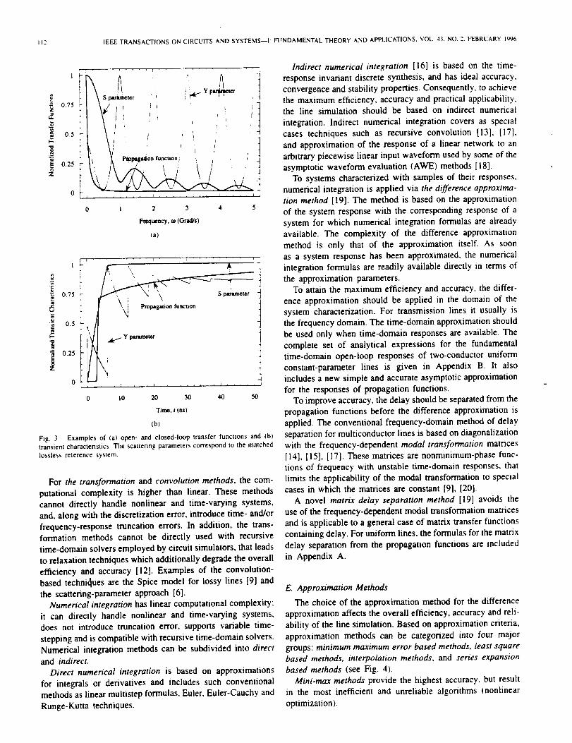
Therefore, one can distinguish between closed- and open-loopcharacterizations.
Closed-loop characterizations (such as Z-, Y-, H- and S-
parameter characterizations [6], [7]) include reflections from
the terminations and lead to complicated oscillating transfer
functions and transient characteristics (unit-step responses).The open-loop characterization (direct characterization in
terms of the propagation functions) separates forward and
backward waves and results in the simplest transfer functions
and transient characteristics (see Fig. 3). The complexity of thetransfer functions and transient characteristics is an important
factor affecting accuracy and efficiency of the transient sim-
ulation. Consequently, to attain the maximum efficiency and
1057-7122/96505.00 © 1996 IEEE

KUZNETSI)V AND SCHI"T'T-:,,INE: OPTIMAL TRANSIENT SIMULATIt)N ()F TRANSMISSION LINES Ill
Formulation
affects dirncnsmns of the
Line Characterization
affects complexity of the transfer functions, and u'ansientand impulse characterisbcs u._d for the simulation
Transient Simulation Technique
affects compu-,UonaJ efficiency and accuracy of the resulbr
Fig. 1. Aspects of the transmission line simulation.
N+ I..conductor linelVlll
{ed'_ (vsl_ Skpud
1",1_ o_l.cton
[e_lL(_ " RefemececonductorI I,
t'2Jt
Fig. 2. System model for transmission lines. Wvf and Wvb represent
the forward and backward matrix propagation functions for voltage waves:
Tx,,x, Tva and Fv'1, Fva stand for the near- and far-end matrix transmis-
sion and reflection coefficients. 1'2
accuracy, the line simulation should be based on the open-
loop characterization. The complete set of expressions for theopen-loop functions for uniform lines is given in Appendix A.
C. Line Model
Line models can be divided into two large groups: circuit
and noncircuit.Noncircuit models can not be directly integrated into a
circuit simulator. As a result, these models cannot be effi-
ciently applied the transient analysis of real circuits containing
1Throughout the paper, capital boldface, small boldface and normal italic
symbols denote mamces, veclors and scalars, respectively.
Since only multiconductor lines will be considered, the modifier "matrix"
will be ormued in the future for brevity.
thousands of nonlinear active devices. Examples of noncircuit
models are the scattering-parameter model [6] and system
model shown in Fig. 2.
Circuit models can be directly incorporated into a circuitsimulator and are of prime practical interest. They relate
voltages and currents at the line terminals and do not dependon the terminations. Circuit models can, in turn, be subdivided
into equivalent-circuit and device models.
Equivalent-circuit models have a larger number of nodes
than the line they represent. Examples of equivalent-circuit
models are lumped and pseudo-lumped segmentation models[3], modal decomposition models for muiticonductor lines [8],
[3], [9], and equivalent-circuit modeling of the propagation
function and characteristic impedance based on Pad6 synthesis
[lO].Device models have the same number of nodes as the line
they represent. A well-known example of device models isthe method of characteristics [11]-[15]. The circuit simulation
time is cubically proportional to the number of nodes and to
the number of voltage and current variables. Consequently,
to achieve the maximum efficiency and practical applicability,the line simulation should be based on a device model that
does not require the introduction of current variables.
D. Transient Simulation Method
The transient simulation method is the prime factor affectingthe efficiency of the line simulation. The selection of thetransient simulation methods is confined to the numerical
Fourier and Laplace transformations, numerical convolutionandnumerical integration.
112 IEEE TRANSACTIONS ON CIRCUITS AND SYSTEMS--I FUNDAMENTAL THEORY AND APPLICATIONS. VOL 43, NO 2. FEBRUARY 1996
0.75
0.5
0.25
\ s _ime,-r ,_ : r'- '_ "
_, Prpplg_on tuncuon, , , , ; a
I 2 3 4 5
Frequency, _ (Gtzd/s)
(a)
° io.\._ Pmpaga,Uon funcaon t
_ Y parzmem-
, , ]0.25 I
DI , _ , , L , , , , I , , , , I f
0 I0 20 30 40 50
Time, t (ns)
(b)
Fig 3 Examples of (at open- and closed-loop transfer functlons and {b)
transient characteristics. The scatterun_ parameters correspond to the matched
Iossless relerence system.
For the transformation and convolution methods, the com-
putational complexity is higher than linear. These methodscannot directly handle nonlinear and time-varying systems,
and, along with the discretization error, introduce time- and/or
frequency-response truncation errors. In addition, the trans-
formation methods cannot be directly used with recursive
time-domain solvers employed by circuit simulators, that leads
to relaxation techniques which additionally degrade the overall
efficiency and accuracy [12]. Examples of the convolution-
based technit_ues are the Spice model for iossy lines [9] and
the scattering-parameter approach [6].Numerical integration has linear computational complexity;
it can directly handle nonlinear and time-varying systems,does not introduce truncation error, supports variable time-
stepping and is compatible with recursive time-domain solvers.Numerical integration methods can be subdivided into direct
and indirect.
Direct numerical integration is based on approximations
for integrals or derivatives and includes such conventional
methods as linear multistep formulas, Euler, Euler-Cauchy and
Runge-Kutta techniques.
Indirect numerical integration [16] is based on the time-
response invariant discrete synthesis, and has ideal accuracy,convergence and stability properties. Consequently, to achieve
the maximum efficiency, accuracy and practical applicability,the line simulation should be based on indirect numerical
integration, Indirect numerical integration covers as special
cases techniques such as recursive convolution [13], [17],
and approximation of the response of a linear network to an
arbitrary piecewise linear input waveform used by some of the
asymptotic waveform evaluation (AWE) methods [18].
To systems characterized with samples of their responses,numerical integration is applied via the difference approxima-
tion method [19]. The method is based on the approximation
of the system response with the corresponding response of a
system for which numerical integration formulas are already
available. The complexity of the difference approximation
method is only that of the approximation itself. As soon
as a system response has been approximated, the numerical
integration formulas are readily available directly in terms of
the approximation parameters.To attain the maximum efficiency and accuracy, the differ-
ence approximation should be applied in the domain of the
system characterization. For transmission lines it usually isthe frequency domain. The time-domain approximation should
be used only when time-domain responses are available. The
complete set of analytical expressions for the fundamental
time-domain open-loop responses of two-conductor uniform
constant-parameter lines is given in Appendix B. It also
includes a new simple and accurate asymptotic approximation
for the responses of propagation functions.To improve accuracy, the delay should be separated from the
propagation functions before the difference approximation is
applied. The conventional frequency-domain method of delay
separation for multiconductor lines is based on diagonalization
with the frequency-dependent modal transformation matrices
[14], [15], [17]. These matrices are nonminimum-phase func-tions of frequency with unstable time-domain responses, that
limits the applicability of the modal transformation to special
cases in which the matrices are constant [9], [20].
A novel matrix delay separation method [19] avoids the
use of the frequency-dependent modal transformation matrices
and is applicable to a general case of matrix transfer functions
containing delay. For uniform lines, the formulas for the matrix
delay separation from the propagation functions are included
in Appendix A.
E. Approximation Methods
The choice of the approximation method for the differenceapproximation affects the overall efficiency, accuracy and reli-
ability of the line simulation. Based on approximation criteria,
approximation methods can be categorized into four major
groups: minimum maximum error based methods, least squarebased methods, interpolation methods, and series expansion
based methods (see Fig. 4).
Mini-max methods provide the highest accuracy, but result
in the most inefficient and unreliable algorithms (nonlinear
optimization).

KI'ZNETSOV AND g['HI"T'r--_.INE ()PTIMAL TRANSIENT SIMULATION ()F TRANSMISSION I_INES II "_
gh accuracy I
mputauonally exlensnve |utre a large number of original |
tton samples •
_llni-Max Method-, "_• the highest accuracy /• the mosl complex, unreliable and /computatnonally extenswe methods|(non, near olxirnlzation ) l• recluure a large number of original |
_ncnon samples •
_nterpolllt Ion Method|
(point fining) |,
•thes_mpl_tandmoucoml_w I_onally efficient methods I I• reqmre the fewest number of on- Isinai function samp[_ (the number I iof samples LSequal to the number ofI[he approximauon parame_zs_ •
_eries EXl_uion _-Nd"
Methodl
• the Ix)ofett accuracy• computalaonally efficient• reqture e_e funcuonaI represen-tation of the oril_md funclion of alarge number of samples• can IXovnde closed fcxmulas forthe apprommaOon parameters ttfunctional representauon of the ori-
_mal funclmn )s available ,a
Fig. 4, Approximation methods.
TABLE I
COMPARISON OF APPROXIMATION METHODS
ApproxtrnaUo_ Method
Mini-max approxm,.auoo
Least squares approxamauon
Interpolation
Economized rauonal approximation
Pad_ syud_r_is at zero
Pad_ SynOd.SiS at infinity
Maxunum _ Relaave
Relative Error ! runtanei
0.0004% 200
0.002% 50
0.003% 1.0
0.004% 2,0
0.06% 1,3
0.3% 1,5
Least square methods provide high accuracy, but are still
computationaily extensive. The examples of least squaresbased methods for the time-domain difference approximation
are Prony's method [21] and pencil-of-function method [22].
Series expansion based methods (such as PadE synthesis
used for the AWE [23]-[25]) are computationaily efficient,
but provide the poorest accuracy.Interpolation (point-fitting) [19] agrees exactly with the
original function on a given set of samples. It provides highaccuracy for simple functions, such as open-loop transmission-
line responses, and is the most efficient among the approxima-
tion methods. It also requires the minimal number of the orig-
inal function samples, which is important when the samples
are obtained from electromagnetic simulations. Consequently,
to achieve the maximum efficiency, the line simulation should
be based on interpolation.
Table I presents the typical values of the maximum relative
error in the full frequency range from zero to infinity andrelative runtime for various approximation methods as applied
to the third-order frequency-domain difference approximation
of open-loop transmission-line functions. Economized rational
approximation starts with the PadE synthesis, which is not
accurate away from the expansion point, and then pem,u'bs it to
reduce the leading coefficient of error in a given approximation
interval [23], [24].As one can observe, interpolation provides accuracy com-
parable with that of the least square approximation, and
is 200 times more efficient than mini-max approximation.
Interpolation is also up to two orders of magnitude more
accurate and 30-50% more efficient than Pad6 synthesis.
Note also that, because of the simplicity of the open-loop
characterization, a very high accuracy is achieved with as low
as third-order approximation and as few as seven samples ofthe original function used for the interpolation.
F. Summa_. of Optimal Approach
To summarize, the analysis of the problem showed that
to achieve the maximum efficiency, accuracy and practical
applicability, the line simulation should be based on
• time-only formulation;
• open-loop characterization:
• device model that does not require the introduction ofcurrent variables;
• indirect numerical integration;
• frequency-domain difference approximation based on the
interpolation and matrix delay separation.
A method close to the optimal, but based on the time-
domain difference approximation, was first proposed by Sem-
lyen and Dabuleanu [17], and was further developed byGruodis and Chang [15] to accommodate the frequency-
domain approximation. The advantages of the approach were
recognized only in recent years, and an increasing number
of techniques close to optimal are published [13], [141, in-
cluding techniques based on the AWE, recursive convolutionand method of characteristics, and by researchers previously
advocating transformation and direct convolution techniques.
The applicability of the methods, however, had been limited
by the lack of accurate, reliable and efficient frequency-
domain approximation and delay separation techniques such as
interpolation-based approximation methods and matrix delayseparation [19], and by the lack of open-loop models fornonuniform lines.
The authors' implementation of the optimal method for uni-
form lines is outlined in the next section. The implementationof the method for nonuniform lines is described in [26].
III. IMPLEMENTATION OF OPTIMAL
METHOD FOR UNIFORM LINES
A. Frequency-Domain Line Model for Transient Analysis
The frequency-domain element characteristic (for the tran-
sient analysis) which does not require the introduction ofcurrent variables and is suitable for the line modeling, is given
by
il(w) ----Yl(_)vl(ua) - Jl(_)i2(_,) Y2(_)v2(,,,) j2(_'). "'
The conventions for the terminal voltages and currents are
shown in Fig. 5. The expressions relating the matrix admit-
lances Y] and Y_ and vector current sources jz and j2 to the
transmission line characteristics are derived directly from the
continuity conditions for the voltages and currents at the lineterminals. To separate forward and backward waves and open
the feedback loop, the current source Jz must depend only on

114 IEEE TRANSACTIONS ON CIRCUITS AND SYSTEMS_I: FUNDAMENTAL THEORY AND APPLICATIONS. VOL 43. NO 2. FEBRUARY 1996
Fig. 5.
li0--2 I'v h
l.l '[ill _ [vt]:'1.2=_
I.N ,[il--_lN [vt }_÷
N+ I-conductor line
Sillml--, ' ,
lMtmm*_
lh],[vl]l [_2_ 2, I
[vl]2 _ 2.2
[,21_ fh]__- 2JV
÷
- = 2'
Conventions for the voltages and currents at the line terminals.
the backward wave, and J2 only on the forward wave. This
condition uniquely defines Y1,Y2 and jr,j2 as follows:
and
Yx(_) = Y2(w) = Y:(w) (2)
j](w) = 2ibl(w)j2(w) 2in(w). (3)
where Yc stands for the characteristic admittance, and the
forward and backward current waves, in, in and ibX, ib2 arerelated as follows:
ibl(w) = Wlb(Co)[ib2(W) = i2(w) --t- in(w)]in(w) = Wu(w)[ifl(w) = il(w) + ibl(w)]. (4)
For uniform lines, the propagation functions for the forwardand backward current waves are equal, W]r = WIb. The
propagation function and characteristic admittance can becomputed from the insertion loss data [15], scattering param-
eters [27], or distributed RLGC parameters (see AppendixA).
As can be observed, for uniform lines, the open-loop device
model (1)--(4) is equivalent to the generalized method ofcharacteristics [12], [13], [15]. However, for nonuniform lines,
the generalized method of characteristics no longer separatesforward and backward waves and loses physical meaning [26].
B. Difference Approximation
To perform the transient analysis, indirect numerical in-
tegration [16J is applied to the propagation functions andcharacteristic admittances in the frequency-domain line model
(1)--(4) by using the difference approximation method [19].
For the difference approximation in the parallel canonic
form, samples of the frequency-domain transfer function are
approximated with the rational polynomial function
M
am
H(jw) = B_ + Z 1 + jw/w..," (5)m=O
or samples of the time-domain unit-step response are approx-
imated with the exponential series
M
h(t) = [-Io - _ a,,,e -_''t,m=l
where /2/0 and /i/z, denote the initial and final values of the
approximating transfer function [l(jw).
Once the approximation has been performed, indirect nu-merical integration formulas (discrete-time difference equa-
tions) are readily given in terms of the approximation param-
eters. For the step invariance the formulas are
y(t.) = 9_z(t°) + Z z,.(t.)rn=]
z,,_(tn) = a,,_(1 - e .... r. )z(t,__x) + e .... r. z,.(t,__l ).
(6)
where z, y and zm stand for the excitation, response and state
variables, respectively, and 7". = t,_ - t,__ x is the time stepat the nth transient iteration.
For the ramp invariance
( My(t.) = Ho*(t.) - _--_:_(t,,)rrt=|
zm(t.) = d,_(T.)(z(t.) - x(t.-l)) + e .... r"zm(t._l).
(7)
where
i - t_-''_T"d_(T.) =_
Wcra Tn
An alternative form of the ramp-invariant indirect numerical
integration formula has the coefficients of the present-time
sample of the excitation lumped together
{ ( " )y(t.) = [to- Z d,,_(T.) z(tn)- Z zm(t,_),,_=x ,,=1 (8)
zm(t,_) = (dm(T,__l)e -_`_T_' - dm(T.))z(t,_-l)
+ e .... r"zm(t,_l).
This form is especially suitable for discretization of charac-teristic admittance, because, for admittances, the present- and
past-time terms of the numerical integration formulas have
different physical meanings.
Before the approximation, the delay is separated from the
matrix propagation function using the matrix delay separation
formulas from Appendix A. and is modeled separately using a
low-order spline of the simulated time points. The differenceapproximation is applied to each element of the delayless
propagation function and characteristic admittance matrices.For the characteristic admittances in (1), the excitations are the
terminal voltages and the responses are the terminal currents.
For the propagation functions in (4), the excitations and
responses are the current waves.
Since the open-loop functions are aperiodic, they have to
be approximated with only real poles, -we,,,. In addition, thepoles have to negative to be assure stability.
To represent the original functions accurately with the
minimum number of samples, the variation of the original
function from sample to sample should be about the same.
The following empirical formula for the sampling frequencies
was found to provide good results
w_=wh- 1-cos . k=0,1,..-.K.
The end of the approximation interval, wh. should be cho-
sen so that the original function would closely approach its

KUZNETSOV AND SCHU'I-r-AINE: OPTIMAL TRANSIENT SIMULATION OF TRANSMISSION LINES 11 _.
final value. This assures that the resulting indirect numerical
integration Ibrrnuias will be accurate in the full frequency andtime ranges from zero to infinity•
C• Interpolation-Based Complex Rational Approximation
Method for Frequency-Domain Difference Approxzmation
The method fits samples of a complex transfer functionH(tu I with the rational polynomial function (5) at the set of
arbitrary spaced frequencies {0. wl. _2,' ". tub-}. The method
proceeds in three steps•
First, the real part of the original function is fit with the real
part of the complex rational polynomial function, which is a
real rational polynomial function of squared frequency [19]
Re([-l(jw)) = co + et_u 2 + c_(_2) 2 + ... + cAt(cu") At ¢9)1 + /_1 we + /32(W2) 2 + ''" + /3M(w2) M "
The following linear system of equations (10) (see bottom of
the page) results from matching the real part of the originalfunction with (9) at the set of frequencies and premultiply-
ing both sides of each equation with the denominator For
interpolation, K = 2M and solving (10) produces a rational
polynomial function which coincides with the real part of theoriginal function at all of the sampling points. For a set of
samples larger than 2M + 1, the least square solution of (10)
can be obtained. However, it minimizes the approximation
error premultiplied by the denominator, which can lead to
inaccurate approximation. Better results are achieved with the
method of averages [28], which partitions the larger number
of equations into 2M + 1 subsets in the order of the increasingof _. The equations within each subset are added up, which
makes the system consistent. The method is effective in
averaging out the noise in measured data.
After the real part has been approximated, the denominatorof (9) is factored yielding the squared poles, 2 Conse--- _Jcrrt •
quently, no unstable fight-half-plane poles can be produced.However, there still can be spurious complex conjugate and
purely imaginary poles, which are removed. The remaining
real negative poles are used to formulate the equations for the
partial expansion coefficients, am, of (5). As a result, the order
M of (5) is less or equal to that of (9).
Matching the real and imaginary parts of the originaltransfer function H(w) with the corresponding parts of (5)
at the set of frequencies {0, wl,,;2,'",,;h'} leads to the
following linear system of equations
A
0
0
1 ' ' " 1
! 1
I+ _(/_',--'i l " '+ ""i"t _'," _t
l 1
--_I/U.}r I
l + _/_,
--t,d h"/cd: I
)i + _vh• ,vF.1
I
• cz
Ho
Re(H(_I))
Re(H(_h. ))
Ira(H(_t))
.ImtH(_K)).
_11)
For interpolation, M = 2K. and both real and imaginary partsof the original transfer function are matched exactly at all of
the K frequency points and dc. For an arbitrary larger numberof points, the least square solution of (I 1) is obtained from
ATAx = AYb.
The total computational complexity of the approximation
method is that of two real linear solutions and one polynomial
factoring. The orders of the polynomial and linear systems
depend only on the order of the approximation and not on thenumber of the original function samples. Since no iterative orrelaxation techniques are involved, the method is free from
convergence problems. The method can be extended to match
exactly the initial and final values of the original function andto perform a complex-pole approximation [19].
Fig. 6 shows an example of the fourth-order approximation
of an open-loop transmission-line transfer function. As can be
observed, although only nine samples of the original function
were used, the approximation exhibits an excellent match in
the full frequency range. In general, due to their simplicity, theopen-loop functions can be accurately fit with the 3rd-9th-order approximation•
Ii 0 --. 0
w_ ... w_ M
•.°
-w_Re(H(w,)) ...
-w_Re(H(wK))
co
0
--W21M Re(H(wl )) c_...._I
• . -w_MRe(H(wK)) :
tiM.
= Re(H(w'))
.Re( H'(wK ) ) J
(I0)

116 IEEE TRANSACTIONS ON CIRCUITS AND SYSTEMS--I: FUNDAMENTAL THEORY AND APPLICATIONS, VOL 43. NO 2. FEBRUARY 1996
KCLat
node:
1.1
I.N
2.1
2.N
2'
VLI ... VLN
-EI_1],, .... E[_',],,ll| #ml
Vf
/¢
--_'=F -- -£E[_',I,,
VIj ... VIN V2'
-- ff-
I
ff--_-7--
I '
2 I _"r_, _
_ - _ . _-_
-x[*,Jo....z[*,l,.
a._ {J,k
j .-,z.q]
(14)
0.00376
_' 0,00374
=_
._ 0.0O372
.p
0.0037
"8
0.00368
0.00366
0 50 I00 J50 200 250 300
Frequency, o) (Mrad/s)
(a)
001
_. 0.005
o.r.
_ -o._
-0.01
f.-0.015
Freque_y. _ (Mind/s)
(b)
Fig, 6. An example of the 4|h-order complex rational approximation. The
original function is shown by the thin continuous curves and the approximating
function by the thick dashed curves.
D. Companion Model
By applying the difference approximation to the propagation
function and characteristic admittance, the frequency-domain
1.1 '[il}l Ivlll
1.2 --[il 1_ [v112
J_ {,,].t.N ,
1':
Fig 7.
Li_l,ll I I
[vz)I [i_ll 2 Ii{ill| Ivz}: Ilzl z,, _. 2.2
I " :l %_" .
• I I tN., [.{_,lstt,l__, 2.N
Companion model for a transmission line,
element characteristic {1) is transformed into the followingdiscrete-time element characteristic, or companion model
{ il(t,,) = _'a(tn)V_(tn) --j_(t,) (12)iz(tn) "Yz(tn)Vz(tn) - j:(tn).
The circuit-diagram interpretation of the companion model isshown in Fig. 7.
The admittances Y_ and Yz represent present-time co-
efficients in the indirect numerical integration formulas forthe admittances Yz and Y_. The current sources j] and j_
combine the currents jv, and jy_, which correspond to the
remaining parts of the numerical integration formulas for the
admittances, and J1 and Ja, which are given by the discretized(3) and (4)
jl(t,) = -Jvl (tn) +j_(t,) (13)j2(t.) -jy,(tn) + j2(t,,).
Equations (3) and (4) do not contribute to the admittance part
of the companion model because the propagation functions
contain a delay•
The Modified Nodal Approach (MNA) stamp corresponding
to the companion model (12) is (see (14) at the top of the
page).
In the circuit simulator during the transient analysis, the
lines are represented by the tables of numbers (14), whichare recursively updated at each time iteration using numerical
integration. The left-hand side of the stamp (14) has to be
updated only when the value of the time step changes. If the
step-invariant indirect numerical integration formulas (6) are

K 17ZNETSOV ,AND ";('HI '77. -'_INE OPTIMAL TRANSIENT SIML!LATION r)F TRANSMISSION LINEN I I ?
KCL at
node;
1.1
I.N
2.]
2.N
2'
I Iv,, ... v_,, __1 v, .-
I-£[v,,_, I
y I ,-': II .,,ll I-,Y_..[Y,,l,,, I
-Y[Y,,L, .... Y[Y,,],,,, I _'Y'-[V,,l,, IJ_l J=l JII J_l
t _- tI-EIY,,I,, f
y /slI " I21 N II -]_[v,,l,,,,
__ _ L_-___' I
-,t,,,,l,,....
V2._ ,.. V:., Vz
-ZtY,,1,,
YI2 "':-y_[v,,l_,
--, _------I-_- --_-Y[v,,], , .... Y Iv,,],,, i 'F.Y.[v,,],,
11-,X.,[v"l,,Y ,
22 I "-Z[Y-],,
Vu
Vt,
Vru --
Va_
Y2._,
Vz
0
oI
--i 0
, ,.,.d I
0
o
0• o
{161
used. the LHS of the stamp becomes independent of the time
step, and only the right-hand side vector has to be updated.Since the terminal currents are not introduced as variables,
the values of il and is in (4) are computed from (12).
E. Line Model for AC and DC Analyses
For ac and dc analyses, the complexity of the transfer
functions is not important, and the element characteristic that
does not require the introduction of current variables and is
suitable for the ac/dc modeling of transmission lines is the
Y-parameter characteristic
{ i1(_) = Yll(tv)vl(_) + Yt2(_)v2(_! (IS)i2(w) Y21(tv)vl(tv) + Y22(_)v2(_v).
The ],'-parameters are related to the open-loop functions asfollows:
Ylx(_) = Y2z(_)
= Y°(,,.,)+ 2[i - w_(_)l-'W_(,.,)vo(_).Y1'_ (w) = Y2x (_) = -2[I - W_(_)]-ZWi(_)Yc(o.,),
where I is the identity matrix. The expressions were derived
by eliminating jl and j2 from (1)-(4), and transforming them
to the form of (15).
The dc model is merely the ac model at zero frequency. For
the limiting case of lines with zero distributed conductance,
G = O, the dc values of the Y-parameters are
Yla(0) = Y22(0) = -Ya_(0) = -Y_x(0) = _R -_.
The MNA stamp corresponding to (15) is (see (16) at the
top of the page).
F. Initial Conditions for Transient Analysis
The dc model is used to perform the operating-point (op)
analysis before the transient simulation. The op solution isthen used as the initial conditions for the transient analysis.
The initial conditions for the indirect numerical integration arethe dc values of the state variables, which are related to the dc
value of the excitation, .Co. as follows: zm(to) = a,_.r,_ for the
step-invariant case (6), =m (to) = 0 for the ramp-invanant case
{7), and z,,(to) = -dm(T_)xo for the ramp-invanant case
(8)• The dc values of in and ibU. which serve as excitations
for the propagation functions in (4), have to be expressed in
terms of the terminal voltages obtained from the op analysis•
Resolving (1)--(4) leads to
in(O) = [I -W_(O)]-I[Ye(O)v,(O)
-W_(O)Y_(O)va(O)]
ibm(O) = [I-W_(1)]-'[Y,(O)v_(O)
-wt(o)Y¢(o}v_(o/J.
For the limiting case of G = 0. the expressions become
1in(O) = --ibm(O) = _R-a[v_(O) - v_(O)].
G. Optimal Line Simulation Algorithm
For an MNA-based simulator, the optimal line simulation
algorithm is as follows:
1) Before the transient analysis:
a) Perform op analysis of the circuit to find the initial
conditions for the transient analysis. Use the ac/dcmodel (15)-(16).
b) For each line in the circuit, perform the difference
approximation of each element of the propagationfunction and characteristic admittance matrices.
2) At each time iteration: Recursively update the line
stamps using the indirect numerical integration formulas
obtained at step l(b) and companion model (12)--(14).
Since the method introduces neither additional nodes nor
current variables, the optimal line modeling does not increase
at all the circuit solution time• The only additional time is
required to perform a low-order interpolation once in thebeginning of the simulation, and for a low-order numerical in-
tegration. As shown in the next section, this time is negligiblysmall compared to the circuit solution time•
118 IEEE TRANSACTIONS ON CIRCUITS AND SYSTEMS--I: FUNDAMENTAL THEORY AND APPLICATIONS. VOL. 43. NO 2. FEBRUARY 19_
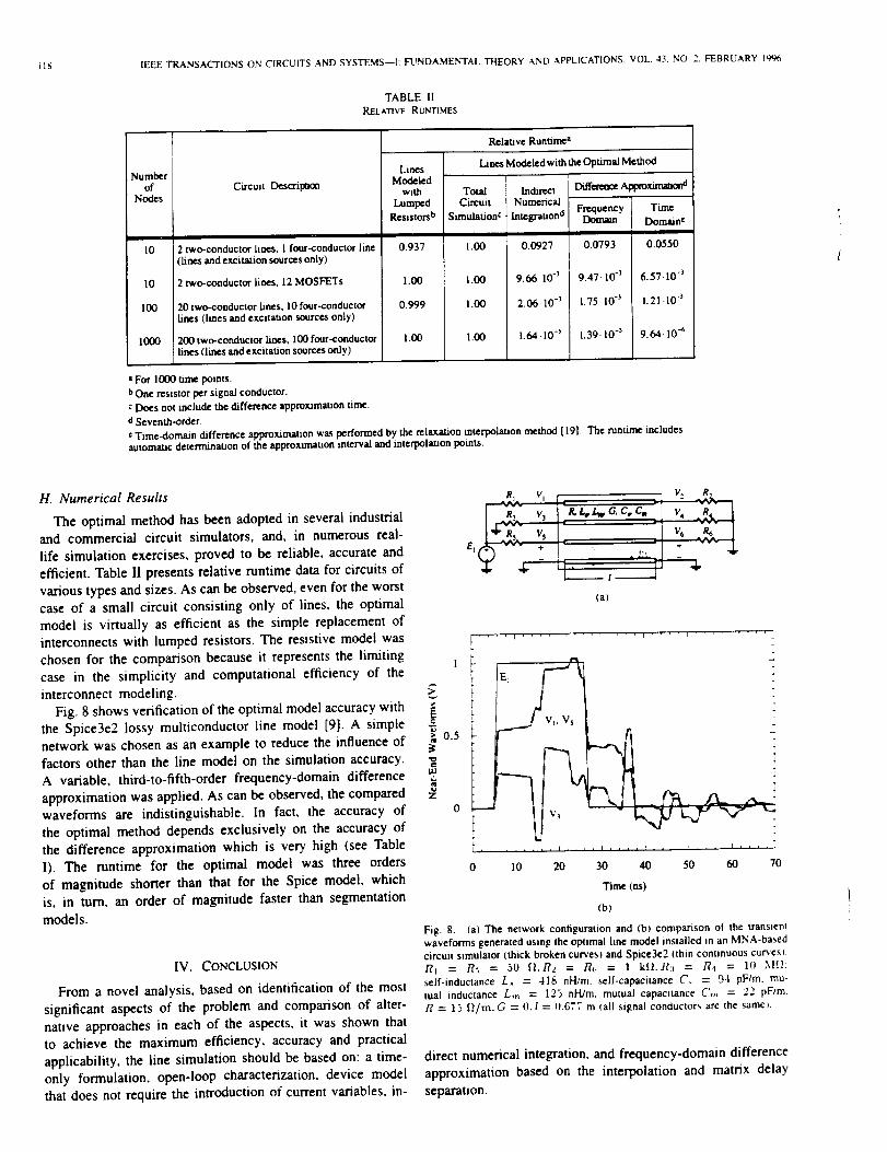
TABLE II
RELATIVE RUNTIMES
Numberof
NodesC_cuit Descnp_on
10 I 2 two-conductor lines, 1 four-conductor line(fines and excitation sources only)
10 2 two-conductor lines, 12 MOSFETs
100 20 two-conductor lines, 10 four-conductorlines (lines and excitation sources only)
1000 200 two-conductor lines, 100 four-conductorlines (lines and excitation sources only)
LinesModeled
withLumped
Resistors b
0.937
1.00
0.999
1.00
Relative Runtime a
Lines Modeled with the Optimal Method
TotalCircuit
StmulatJon c
1.00
1.00
1.00
1.00
_directNumencal
lnmgrauon d
0.0927
9.66.10 "3
2.06.10 "J
1.64.10 -s
Diffnen_ h4T_ximanond
Frequency TimeDomam Domain c
0.0793 0.0550
9.47.10 "_ 6.57.10 -3
1.75.10 -3 1.21-10 "_
1.39.10 "s 9.64.10 "_
• For 1000 ume points.
b One rcsistor per signal conductor.
c Does not include the difference approxamauon time.
d Seventh-order.
e Time-dommn difference approximation was performed by the relaxation interpolation method [ 19]. The runtime includesautomaUc determmaUon of the approxulnaUon interval and interpolauon pomp.
H. Numerical Results
The optimal method has been adopted in several industrialand commercial circuit simulators, and, in numerous real-
life simulation exercises, proved to be reliable, accurate and
efficient. Table II presents relative runtime data for circuits of
various types and sizes. As can be observed, even for the worstcase of a small circuit consisting only of lines, the optimal
model is virtually as efficient as the simple replacement of
interconnects with lumped resistors. The resistive model was
chosen for the comparison because it represents the limiting
case in the simplicity and computational efficiency of the
interconnect modeling.
Fig. 8 shows verification of the optimal model accuracy with
the Spice3e2 iossy multiconductor line model [9]. A simplenetwork was chosen as an example to reduce the influence of
factors other than the line model on the simulation accuracy.
A variable, third-to-fifth-order frequency-domain difference
approximation was applied, As can be observed, the compared
waveforms are indistinguishable. In fact, the accuracy of
the optimal method depends exclusively on the accuracy of
the difference approximation which is very high (see TableI). The runtime for the optimal model was three orders
of magnitude shorter than that for the Spice model, whichis, in turn, an order of magnitude faster than segmentation
models.
IV. CONCLUSION
From a novel analysis, based on identification of the most
significant aspects of the problem and comparison of alter-
native approaches in each of the aspects, it was shown thatto achieve the maximum efficiency, accuracy and practical
applicability, the line simulation should be based on: a time-
only formulation, open-loop characterization, device model
that does not require the introduction of current variables, in-
R1 V, , V, R.
Ca)
0 I0 20 30 40 50 60 70
Time (ns)
(b)
Fig. 8. Ca) The network configuration and (b) comparison of the trans,ent
waveforms generated using the optimal line model installed in an MNA-based
circmt simulator (thick broken curves) and Spice3e2 Cthtn continuous curves)
/?) = ./7-, = 50 _LBe = /7_, = I klL//:_ = 174 = If) M.Q:
self-inductance L, = 418 nH/m, self-capacitance C, = 94 pF/m. mu-
tual inductance L,,, = 125 nil/m, mutual capacitance C,,, = 22 pF/m.
17 = 13 _/m.G = (1.1 = (1.G77 m fall signal conductors are the same).
direct numerical integration, and frequency-domain difference
approximation based on the interpolation and matrix delay
separation.

KI.ZNETSOV AND 5,('ttL:TT AINE: OPTIMAL TRANSIENT SIMtlL,ATION ()F TRANSMISSION LINKS
TABLE III
Name of Function
Adnuttance and
impedance per unitlength
;Modal[ransfonnauon
rnamccs
Characteristic
adnmtance and
m_pedance
Propagauoncons[a/it b
Propagauon delay b
Propagationfunction b
Delaylesspropagationf_nction b
Transmission
coefficient c
Function forCurrent Waves a
In Standard Basis
Y(o)) = G(eo) + ;o)C(eo)
= Mdo)) Y=((o) Mv1(m)
MI(O))
= Eigenvectors(Y(a)) Z(o))),
_1, = M,(o-)
= Eigenvectors(C(,_) L(oo))
Y,(o_)= KI(co)Z-'(o))
= K_(o_) Y(u))= Z_1(m)
= Ms(o) ) Y.(o)) Mvl(O))
I
Ks(co) = (Y(m) 7_.(co))i
= y(o)) y_l(o))
= Ms(o)} Kt.,(o)) Mi't (o))
I
Tt = (C(-) L(o.))i l
= Kt(--)l= M I T,_ l_4_'
Wt(o) ) = e-'C,.._ J
= Mr(mS Wl=(o}) M_t(m)
= Y.((o) W,,(o)) Z.((o)
= _V,(_o)e"''t'
= w,(o)) N4,e-'" Nt,'
Wt(o)) = Ws(o)) e _'r,
Ts(m) = (I + YAm) Z.(o))-'
= Y,(co) Tv(CO) Z,(ea)
Reflect/on F, (co) = (1 + Yt(O)) Z, (e0))-'coefficient c
.([ - YAm)z,(o_))
= Y,(o_)rv(m) Z,(m)
In Modal Basis
Y.(o))
= M['(_o) Y(¢_) My(m)
M_'(_) = Mtv (o)),
t
Y.(o)) = (Z2(o}) Y.(o_)) i
= K_=t(o})Y.(O))= Z-_ (to)
= Mi'(o) ) Y,(o)) Mv((O)
I
K,.(O)) = (Y.(O)) Z=(O)))_
= y.(o)) y-t (o))
= Eigenvalues(Kl(o)) )
= M_t(m) Ks(Co) M,((_)
= Kv=(o))
T,.. = Kt.(oo) 1
= FJgeanaum('r,)
= IVl[ I T, M, = Tv=
W,..((o) = e -'_'s'' t
= M_(O)) Wt(o)) Ms(mS
= Wv.(m)
Funcuon forVoltage Waves d
InStandardBas,s
Z(O)) ffi R(_0) +/tO L(OJ)
= Mv(_) Z.(o)) M_'(o))
My(aS)
= Eigenvecton(Z({o) Y(e0)),
I_ v = My(-)
= Eigenvectors(L(-) C.(-))
Z,(oo) = Kv((O) Y-'(m)
= Kv'(m) Z(m) = Y_'(o_)
= My(o)) Z.(o)) M_'(o))
I
K,(m) = (Z(m) Y(m)F
= Z(o)) Z;'(o))
= My(CO) K=(m) M_'(O))
I
Tv = (IX-) C(-))I L
= Kv(--) 1 = P_4v Tv= l_lv s
W v ((0) = e J" c'_
= Mv(_) Wv=(m) M_'(m)
= Z,(_) W_(o_) Y,(to)
= _', (mSe"_r"
= ',Vv(m)M_ e"'_" r_'
VVv (o)) = Wv(0} ) e'_T"
Tv(O)) = (1 + Z,((o) Y.(m))-'
= Z,(o)) T,(m) Y,(m)
F v ((o) = (Z,(w) Y,(o)) + I)-'
.(Z,(w) Y.(o)) ' I)
= Z_(m) F,(m) Y_(m)
In Modal Basis
Z.(o))
= Mv'(m)Z(o)) M,(o))
I
Z.((o) = (Y_(o_)Z=(o)))_
= Kv__(o)) Z=(o)) = Y-_ (o))
= Mv'(tO) Z,((o) M,(_o)
K,.(oo) = (Z.(m) V.(o)))i
= Z=(o_)Z-' (o))
= _geuv_um(K, (o)))
= Mv'(O}) Kv(OO) Mv(O_) =
= K,.. (o)
Tv= = Kv=(") 1
= Etgenvalues(T_)
= IriS' Tv M, = T,...
Wv.,(o)) = e-K-._ o_'
= Mv'(O) ) Wv(O)) My(o))
= W,..(c0)
a Voltage and current functions are related via the following duality replacement rules: V *-_ I. Z ¢-_ Y, R _ G, L ¢-¢ C.!
b Boldface (.)i and e_'_ denote matrix squre root and matrix exponential, respectively.
c For a Thevenin's [erminadon Zº(o_).
L ItS
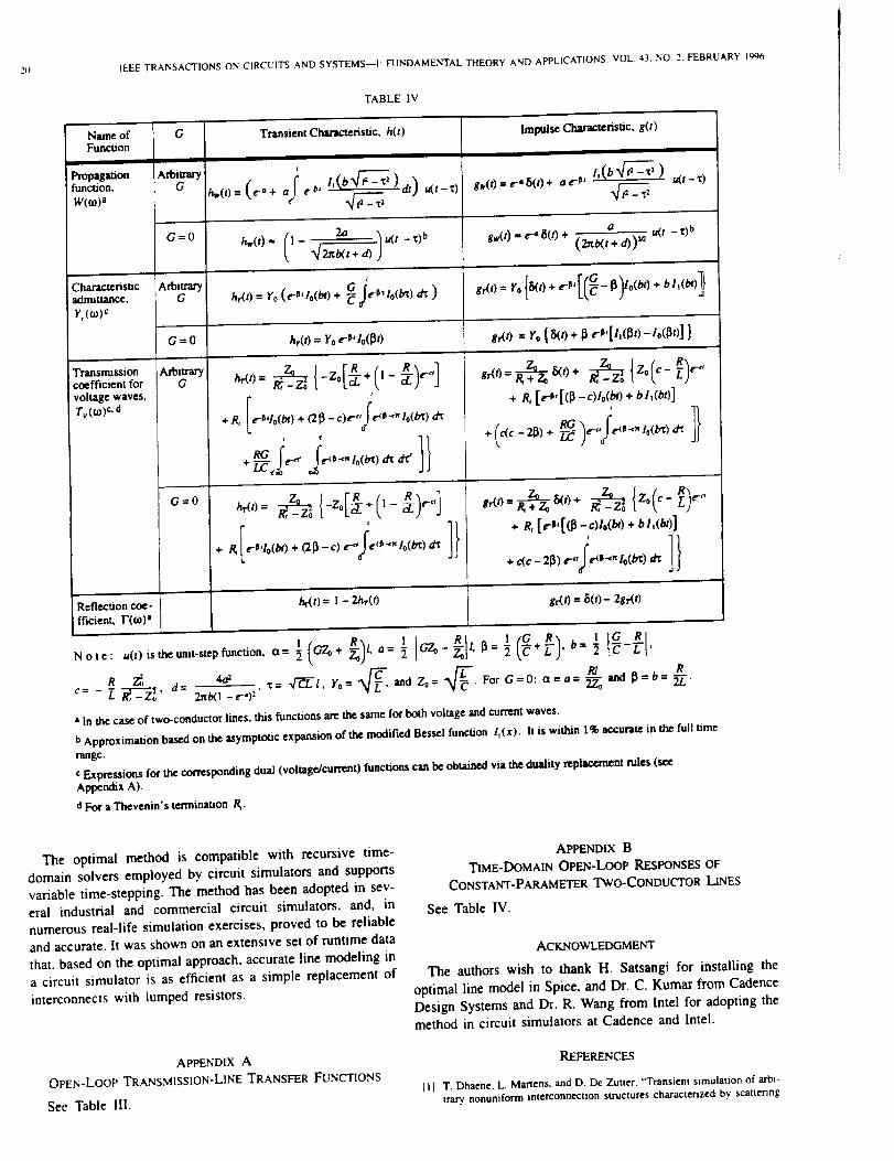
The practical implementation of the optimal method for
multiconductor lossy frequency-dependent lines characterized
by discrete samples of their responses was outlined, includingextraction of initial conditions from op analysis and the line
model for ac/dc analysis. The complete set of expressions for
the open-loop transmission-line functions was given, includingnew formulas for the matrix delay separation from the propa-
gation functions, which avoid the use of frequency-dependent
modal transformation matrices. The complete set of analyt-
ical expressions for the fundamental open-loop time-domain
responses of two-conductor lines was presented, including a
new simple and accurate asymptotic approximation for the
responses of propagation function. The novel interpolation-
based complex rational approximation method was introduced,
and ramp- and step-invariant indirect numerical formulas were
given in terms of the approximation parameters.
:20 IEEE TRANSACTIONS ON CIRCUITS AND SYSTEMS--I: FUNDAMENTAL THEORY AND APPLICATIONS, VOL. 43, NO 2. FEBRUARY 19q6
TABLE IV
Name ofFunction
Propagation! funcuon,
W(_0) a
Chatac_nslJcadmittance,
L(o_)c
Transmzssioncoefficient forvoltage waves,
rv (t_)c, d
G
G=O
G=O
ArbitraryG
G=O
Reflection coe-
fficient, F(c0) a
Transient Characteristic, h(t)
i
t
hw(t) = (I ,2n
ImpulseCharacteristic,g(t)
8w(t)- e--8(0 + a u(t- :)b(2_b(t + d))"_
[(I }h,(,) = Yo (e-th 'o(B¢) + £ :e-lS, 'o(_)d_ ) ,r(t) = Yo {S(t) + e-is, -,)o(bt)+bl,(bO
h,(,)= ro _-_,_0(13,) =_t) = r, {_,) + I e-p'[t,(lo-t°(It)] }
+ R, _'lo(bt) + ('21-c)_'+of_'<"io<_)
+ _- e-_ _'_" t'0(_) a_ dr'
" r., i+ g e-_'lo(b0+ (213-c) •-_ ___"_/o(b¢)d_o"
g_(t)= R, + Z_
=,>. {z°(._I)--+ R,[_-,,[(p- c)1o(_,)+ bt,(_,)]
t
hr(t)= I - 2At(r) gr(t)= 8(0- 2gr(t)
'(1_.) INote: u(t) is the unit-step function, or= ,_ GZo+ 1, a= ½ GZo- l, [3= I(l.I).,-c= - _ J_--_o ' d= 2nb(l -e',):' x= ,/-_-l, Y0 = and Z0= . For G=O: otto= _00 and _=b= _.
a In the caseof two-conductor lines, this functions are the same for both voltage and current waves.
b Approximation basedon the asymptouc expansion of the modified Besselfunction I_(x). It is widdn I% accurate in the full timerange.
c Expressions for the corresponding dual (voltage/current) functions can be obtained via the duality replacement rules (seeAppendixA).
dFor a Thevenin'sterminationR;.
The optimal method is compatible with recursive time-
domain solvers employed by circuit simulators and supports
variable time-stepping. The method has been adopted in sev-
eral industrial and commercial circuit simulators, and, in
numerous real-life simulation exercises, proved to be reliable
and accurate. It was shown on an extensive set of runtime data
that. based on the optimal approach, accurate line modeling in
a circuit simulator is as efficient as a simple replacement of
interconnects with lumped resistors.
APPENDIX A
OPEN-LOOP TRANSMISSION-LINE TRANSFER FUNCTIONS
See Table lit.
APPENDIX B
TIME-DOMAIN OPEN-LOOP RESPONSES OF
CONSTANT-PARAME'IER TWO-CONDUCTOR LINES
See Table IV.
ACKNOWLEDGMENT
The authors wish to [hank H. Satsangi for installing the
optimal line model in Spice, and Dr. C. Kumar from Cadence
Design Systems and Dr. R. Wang from lnte[ for adopting the
method in circuit simulators at Cadence and Intel.
REFERENCES
[I] T. Dhaene. L. Martens. and D. De Zutter. "'Transient simulation of arbi-
trary nonuniform interconnecuon structures charactenzed by scattenng
KL'ZNETSOV -kND SCHt TF-.XlNE oPTIMAL TRANSIENT SIML'IATIt)N ()F TRANSMISSI()N 1.INKS 121
parameters." IEEE 1)'ans. Circuas Svst.. ',ol. 39, pp. 928-937. Nov.I q92.
[2] J. E. Bracken. V Raghavan. and R. A. Rohrer. "Interconnect ,,mmlauon
w_th asymptottc wavelorm evaluation {AWEL'" IEEE Trcms. ('ircmt_
Sv_t,. ',ol. 39. pp. 869-878. Nov. 1992.
131 T Dhaene and D, De Zutlcr. "'Selection of lumped clement models Iorcoupled Iossy transmission lines." IEEE Trans. Computer-Aided De_len.
vol. 11. pp. 805-815. July 1992.[41 K, S. Oh and J. E. Schutt-Ame. "'Transient analysis of coupled, tapered
transmission lines with arbitrary, nonlinear terminations." IEEE Tran_'.
Mictv_wave Theory Tech.. vol. 41, pp. 268-273. Feb. 1993.
[5] D B. Kuznetsov. "'Transmission line modeling and transient simulation,"M.S. thesis. Univ. Illinois at Urbana, 1993.
[6] J. E. Schutt-Ath_6 and R. Mittra. "'Nonlinear transient analysis of coupled
transmission lines." IEEE Trans. Circuits Syst.. vol. 36. pp. 959-967.Jul. 1989.
[7] 1. Maio. S. Pignan. and F. Canavero. "'Influence of the line characteri-
zation on the transient analysis of nonlinearly loaded Iossy transmission
lines." [EEE Trans. Circ'ults Swt.. vol. 41. pp. 197-209, Mar. 1994.18] F. Romeo and M. Santomauro, "'Time-domain simulation of n coupled
transmission lines," IEEE Trans. Microwave Theory Tech.. vol. MTT-35,
pp. 131-137. Feb, 1987_{91 J. S. Roychowdhury and D. O. Pederson. "'Efficient transient simulation
of Iossy interconnect," in Proc. 28th ACM/IEEE Design Automat. Conf..
199 I, pp. 740-745.[101 F.-Y. Chang, "'Transient analysis of Iossy transmission lines with ar-
bitrary initial potential and current distributions." IEEE Trans. Circ'utts
Syst.. vo[. 39, pp. 180-198. Mar. 1992.{I I] F. H. Branm, Jr., "'Transient analysis of Iossless transmission lines."
Proc. IEEE. voI. 55. pp. 2012-2013, Nov. 1967.[12} F.-Y. Chang, "'Transient simulation of nonuniform coupled lossy trans-
mission lines characterized with frequency-dependent parameters, Part
I: Waveform relaxation analysis." IEEE Trans. Circuits Syst.. vol. 39.
pp. 585--603. Aug. 1992.[13] F.-Y. Chang. "Transient simulation of frequency-dependent nonuni-
form coupled Iossy transmission lines." IEEE Trans. Comlnm. Pack.
Manufact. Technol.. vol. 17, pp. 3-14. Feb. 1994.[14] J.E. Bracken, V. Raghavan. and R. A. Rohrer. "Extension of the asymp-
totic waveform evaluation technique with the method of characteristics,'"
in Tech. Dig. IEEE Int. Conf. Computer-Aided Design. 1992, pp. 71-75.[15] A. J. Gruodis and C. S. Chang. "Coupled Iossy transmission line
charactenzation and simulation." IBM J. Res. Develop.. vol. 25, pp.25--41, Jan. 1981.
[16} D, B. Kuznetsov and J, E. Schutt-Ain_. "Indirect numerical integration."
to be published.[17] A. Semlyen and A. Dabuleanu. "Fast and accurate switching transient
calculations on transmission lines with ground return using recur-
sire convolutions." IEEE Trans. Power Appar. Syst.. vol. PAS-94, pp.
561-569. Mar./Apr. 1975.{18] T. K. Tang, M. S. Nak.h/a. and R. Gnffith. "'Analysis of Iossy mul-
ttconductor transmission lines using the asymptouc waveform evalu-
ation technique." IEEE Trans. Microwave Theory Tech.. vol. 39, pp.
2107-2116, Dec. 1991.{191 D. B. Kuznetsov and J. E. Schutt-Ain6, "'Difference approximation," to
be published.[20} C. R. Paul. "On uniform multimode transmission lines." IEEE Trans.
Microwave Theory, Tech.. pp. 556--558, Aug. 1973.
[21] S. L. Marple. Jr., Digital Spectral Analysis. Englewood Cliffs, NJ:Prentice-Hall. 1987. pp. 303-349.
[2-.21 '_ Hua and T K Sarkar, 'Generahzed pcncll-ol-lunct]on method tor
cxlracung poles of an EM ,,,,stem tn_m _ts transient re,_ponse.- II:EEIrltu_. ,'ttltenna_ Propaqat,. _(_1. 37, pp. 229-234, Feb. 1989
1231 C-E. Froberg. Numertt al Mathematics." 17teor_' and Computer Appl,'a-
tion._. Menlo Park. CA: Benlamm/Cummmgs. 1_85.[241 A. Ralston and P, Rabmowltz. A I"ir_t ('our_e tn Numerttal ,Inaix_tg.
2nd ed. New York: McGraw-Hill. 1978.
1251 L. T. Pillage and R, A. Rohrer. '-_symplotlc waveform evaluation
lot ummg analysis," IEEE Trans. Cr,mputer-Atded Design. vol. q. pp.352-366, Apr. 199('1.
[261 D. B. Kuznetsov and J. E. Schutt-Atne. "Efliciem circuit simulation of
nonuniform transmission lines." to be published.
127] J. E. Schutt-Am/_, "'Modeling and simulation of high-speed digital circus!interconnections.'" Ph.D. dissertation, Univ. Illinois at Urbana. 1988.
[281 I. N. Bronshteyn and K. A. Semendyaev. Spravochmk po matematlke.
Mo_ow: Nauka, 1967. p, 578. ¢in Russtant.
Dmitri Borisovich Kuznetsov (S'95) was born onJune 26. 1966. in Moscow, U.S.S.R. He received the
Dipl. lug. degree _urama cura laude, in electromcs
engineenng with a specialization in space elec-tronics from the Moscow Electrotechnical Institute
of Telecommumcauon. Department of Automatics.Telemechanics and Electronics. m 1988. He re-
ceived the M.S. degree m 1993 from the Umverslty
of Illinois at Urbana and is currently pursuing the
Ph.D. degree.From 1987 to 1991 he worked as an electronics
engineer at the Space Research Institute. Academy of Sciences of the U.S.S.R..
Moscow. on the design, manufactunng, testing, maintenance and repair
of computer graphics systems. From 1988 to 1991 he attended the post-
graduate school of the Space Research Institute, specializing in the information
and measunng systems in space research. Since 1991 he has conducted
research in computational electronics, transient simulation, and transmission
line modeling at the Department of Elecmcal and Comlmter Engi_nng.University of Illinois at Urbana.
Jose E. Schutt-Ain_ (M'88) received the B.S. de-
gree from the Massachusetts Institute of Technologyin 1981. and the M.S. and Ph.D. degrees from the
University of Illinois in 1984 and 1988, respectively.
Following his graduation from MIT he spent two
years with the Hewlett-Packard Microwave Tech-
nology Center in Santa Rosa. CA. where he worked
as a device application engineer. While pursuing
his graduate studies at the University of Illinois. heheld summer positions at GTE Network Systems
in Nonhlake, Illinois. He is presently serving on
the faculty of the Department of Electrical and Computer Engineenng at
the University of Illinois as an Associate Professor. His interests include
microwave theory and measurements, electromagnetics, high-speed digital
circuits, solid-state electronics, circuit design, and electronic packaging.

IEEE T&ANSACTIONS ON MICROWAVE THEORY AND TECHNIQUES. VOU 42. NO. 8. AUGUST 199,1 1.1-13
Capacitance Computations in a
Multilayered Dielectric Medium Using
Closed-Form Spatial Green's FunctionsKyung Suk Oh, Student Member, IEEE, Dmitri Kuznetsov, and Jose E. Schutt-Aine, Member. IEEE
Abstractm An efficient method to compute the 2-D and 3-D capacitance matrices of multiconductor interconnects in amultilayered dielectric medium is presented. The method is basedon an integral equation approach and assumes the quasi-staticcondition. It is applicable to conductors of arbitrary polygonalshape embedded in a multilayered dielectric medium with possi-ble ground planes on the top or bottom of the dielectric layers.The computation time required to evaluate the space-domainGreen's function for the multUayered medium, which involvesan infinite summation, has been greatly reduced by obtaininga closed-form expression, which is derived by approximatingthe Green's function using a finite number of images in thespectral domain. Then the corresponding space-domain Green'sfunctions are obtained using the proper closed-form integrations.In both 2-D and 3-D cases, the unknown surface charge densityis represented by pulse basis functions, and the delta testingfunction (point matching) is used to solve the integral equation.The elements of the resulting matrix arc computed using theclosed-form formulation, avoiding any numerical integration.The presented method is compared with other published resultsand showed good agreement. Finally, the equivalent microstripcrossover capacitance is computed to illustrate the use of acombination of 2-D and 3-D Green's functions.
I. INTRODUCTION
°N recent years, the characterization of microstrip disconti-nuities in a multilayered dielectric medium by equivalent
circuits has gained special interest due to the modem develop-
ment of VLSI technology. For an inhomogeneous structure
the modes are hybrid, and the full-wave analysis must be
considered. However, the quasi-static approximation is suffi-
ciently correct when the transverse components of the electric
and magnetic fields are predominant over the longitudinal
components; in other words, the transverse dimensions of
microstrip lines are much smaller than the wavelength. Based
on this quasi-static approximation, we present an efficientmethod to compute the 2-D and 3-D capacitance matricesof multiconductor interconnects in a multilayered dielectric
medium.
Under the quasi-TEM approximation, the capacitance cal-
culation follows from the solution of Laplace's equation
with appropriate boundary conditions. Various methods have
been employed to obtain the solution in two-dimensional
space [1]-[9]. Two commonly used techniques for both 2-D
Manuscript received April 5, 1993; revised October 11. 1993.The authors are with the Electromagnetic Communication Laboratory,
Departmentof Electrical and Computer Engineering. University of Illinoisat Urbana-Champaign, Urban& IL 61801 USA
IEEE Log Number 9402933.
and 3-D capacitance calculations in multilayered structures
are the integral equation method [10], [11] and the domainmethods, such as the finite difference and finite element
methods [12], [13]. In the domain methods, the unknown
potential distribution is solved to compute the capacitanceover an entire domain by either directly approximating the
differential equation with the finite difference equation (FD) or
using the equivalent variational expression in conjunction withthe method of subareas (FEM). The major disadvantage of the
domain methods is that the unknown potential distribution to
be sought is over the entire geometry considered, including the
dielectric regions; hence, it may be computationally inefficient
for the open geometry case even with the use of absorbingboundary conditions to truncate the open geometry. On the
other hand, the integral equation approach first obtains theGreen's function for a layered medium using image theory,
which consists of rather slowly converging infinite series, and
solves for the charge density on the conductor surfaces using
this Green's function as its kernel. As noted in [2] for N layers,
the expression for the Green's function would consist of N - 1
infinite series. Alternatively, the free-space Green's function is
used in [2], [3] to avoid infinite _eries, but additional unknown
charges on the dielectric interface and ground planes, on top
of the unknown charges on the conductor surface, must beincluded. Hence, the dimension of the resulting moment matrix
is substantially increased.
Yet another approach to avoid an infinite summation is to
solve the integral equation in the spectral domain (SDA),where the Green's function is in a closed-form expression;
however, this approach can not be applied to general problems,
e.g., conductor with a finite thickness. In this paper, the
Green's function for the layered medium is approximated
in the spectral domain using exponential functions, which
is equivalent to a finite number of weighted real images
in the space domain. Although complex-valued exponentials,
which are often used in a nonquasi-TEM analysis [14], can
also be employed to reduce the number of weighted images
[15], real-valued exponentials are sufficient to approximate
for quasi-TEM applications, and it further avoids the use
of expensive complex operations. Since the spectral-domain
representations of the Green's function for 2-D and 3-D cases
are identical, the approximation is only performed once for
both cases, and then the equivalent weighted images in the
spectral domain are directly used to evaluate the Green's
functions in the space domain.
001g--9480/94504.00 © 1994 IEEE

14z4 IEEE TRANSACTIONS ON MICROWAVE THEORY AND TECHNIQUES. VOL. 42, NO. 8. AUGUST 1994
Possible P.E.C. ]
4
y'_l ,. 1
:i:i:i:!:i:i:i:i:i:i":::::::::::::::::::::::::::::::::::::::::::::::::::::::::::::::::::::::::::::::::::::::::::::::::::::::::::
::::::::::::::::::::::::::::::::::::::::::::::::::::::::::::::::::::::::::(a)
\\\\_,<,,\\\\\\\\.,_
in Layer I in Layer 2
Co)
Fig. 1. (a) Cross-sectional and (b) planar views of possible configurations of
multiconductors in a multilayered medium• The two figures are not related.
II. GENERAL STATEMENT OF THE PROBLEM
The general geometries of systems of multiconductors em-
bedded in a multilayered medium are illustrated in Fig. 1;
(a) shows a possible cross-sectional view while Co) shows a
possible planar view. An arbitrary number Na of nonmagnetic
dielectric layers are hacked by two optional ground planes
with possible top or bottom locations, and within these layers
an arbitrary number Nc of perfect conductors are placed
throughout the layers with arbitrary orientations and possible
discontinuities. The geometries of the dielectric layers areassumed to be uniform in the x- and z-directions, and the
cross sections and planar geometries of the conductors can be
arbitrary as long as their boundaries can he described with a
piecewise linear function.
The integral equation relating the electrostatic potential
V(r) to the charge density p(r) is
V(r) = I G(r,r')p(r')dr' (1)tf_
where G(r, r') is the Green's function for the multilayeredmedium, and 1"2denotes the surfaces or cross-sectional bound-
aries of conductors for 2-D or 3-D problems, respectively. The
capacitance can be computed by solving this integral equation
for the charge density p(r') with various settings of voltages onthe conductors. We will first concentrate on the determination
of the Green's function G(r, r').
III. APPROXIMATION OF THE
SPECTRAL-DOMAIN GREEN'S FUNCTION
Consider a unit point charge located at the ruth layer at
(x0, Y0, z0) (Fig. 2). By definition, the 3-D Green's function
Fig. 2.
tion.
Cv : '
Y_.-!
• _' :":'_ ...... -'- .... /: _,Y_v?_ ..... y
//?iii_i? m ' i il/fiill/i?il;ii??iilSii?:iiiii_i/i?/iii?ii?I?Sfi -
the geometric configuration used for determining the Green's func-
satisfies Poisson's differential equation:
y, z Izo, yo, zo) = l _(z - xo)_(y - yo)_(z - zo)V2GSD(x,
(2)with the appropriate boundary conditions at the possible
ground planes and dielectric interfaces. Noting that thedielectric medium is uniform in two directions, we can
represent the Green's function and the point source in thespectral domain in terms of its transforms in the x- and z-
directions. The space-domain and the spectral domain Green'sfunctions are then related by
GaD(x, y, z I z0, yo, z0)
i /+°°/+°°= (-'_).,__ ..-_ dadB e-_(_-::°)-_(_-_°)
× GSD(a,y,_lxo, Yo, zo )
(3a)
¢3o(_, _, _ I _o, _o,_o)
= dxdzeJa(::-_:o)+Js(z-zo)
X G 3D(x,y,z Ixo, Y0, Z0)
(3b)
where _so(a,y, fl I xo,yo,zo) is the 3-D spectral-domainGreen's function and a and _ are the transform constants
associated with the x and z directions, respectively. Then, (2)can be written as
_ _ _ _ CSD(_, U,_ Ixo, uo, _o) = _(u - _o).(4)
The general solution of the above equation is given by
GAD(7, y [ ro) = Am,.e-"' + B..,.e "_2_,,,'r , "r= v_J + _2
(5)
where the first subscript ra denotes the layer where the
source is located (source point), while the second subscript
n denotes the layer where the Green's function is evaluated
(observation point). The same expression can be obtained by
Fourier transforming G_m(x,y I Xo, Yo) in the x-direction
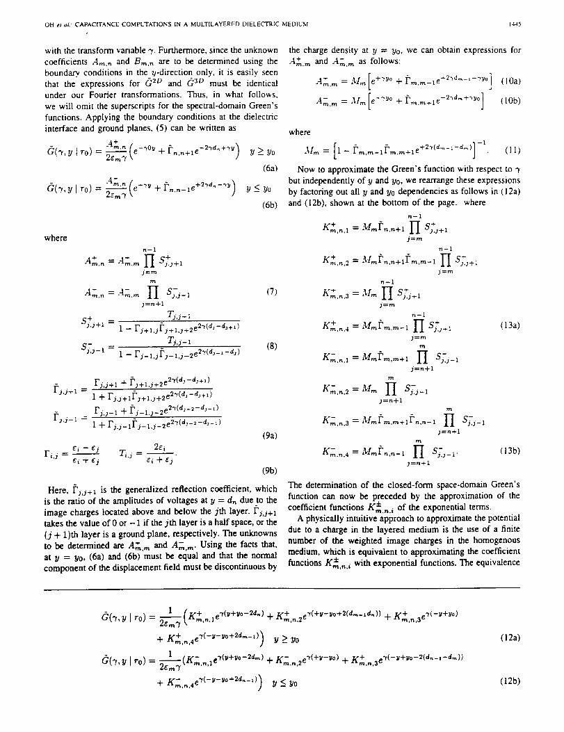
OH el aL: CAPACITANCE COMPUTATIONS IN A MULTILAYERED DIELECTRIC NIEDIUM 14-15
with the transform variable % Furthermore, since the unknown
coefficients A,..,,_ and B,._,. are to be determined using the
boundary, conditions in the _-direction only, it is easily seen
that the expressions for _2D and _3D must be identicalunder our Fourier transformations. Thus, in what follows,
we will omit the superscripts for the spectral-domain Green's
functions. Applying the boundary conditions at the dielectricinterface and ground planes, (5) can be written as
A+."(e-'m_ +Fn,n+le-2"_d.+_Y)
AZ ,, " - _, .+2_d.--,_d('1, y t r0) = .... + ]
Y>Yo
(6a)
Y_< yo
(6b)
where
n-1
+ +AT... = A,,,,,,_ H S+j,j+l
3=m
A=,. fi sL_ 3=n+1
S+ = _ Tjj÷Ijj+l
I -- Fj+l,j['j+l,j+2e 2"r(d:-d:+t)
Tj,j-1
SL 1=' - 1 - Fj_l,jf'j_lj_2e 2"t(a,-'-d:)
(7)
(8)
Fj,j+I =
I'i,j- 1 -=
Fj,j+I + _.j+l.j+2e2-r(d:-dj+,)
1 + Fj,j+lf'j+l,j+2 e2"r(d: -d:+, )
Fj,j-1 + f'j-l,j-2e 2Md:-2-gJ-l)
1 + Fj,j-1Fj- 1,j-2e 2"r(d:- _-d: __)
Fij -- ei --e) Tij 2¢i
' ¢i + ej " ei + sj
(9a)
(9b)
Here, I'jj+_ is the generalized reflection coefficient, whichis the ratio of the amplitudes of voltages at y = dn due to the
image charges located above and below the jth layer, f'./j+l
takes the value of 0 or -1 if the 3th layer is a half space, or the
(j + 1)th layer is a ground plane, respectively. The unknowns
to be determined are A+,m and A_.,m. Using the facts that,
at y = Yo, (6a) and (6b) must be equal and that the normal
component of the displacement field must be discontinuous by
the charge density at y = Yo, we can obtain expressions for4-
Am. m and Am. m as follows:
.4,._,., = M,. e +'r_'° + F,,_ m-xe "'%d_-'-'a,° (lOa)
A_, m = ,'lm[e -'_° + ['m.m+le -2-'d_''_°] (10b)
where
31,,_= [l-f" .... 1Fmm*le+2"_(d"-_-d_)] -1 (11)
Now to approximate the Green's function with respect to "7
but independently of y and Yo, we rearrange these expressions
by factoring out all y and Yo dependencies as follows in (12a)
and (12b), shown at the bottom of the page. where
rt--1
+ = Mr.t..+1 ]-I s+Kin,ha , j,2+ lj=m
n--I
K+n,2 = M,._[',_,,_+lr'._,,,_-i II SJ,"J+Ij----m
n-1
-eK .... a = Mr. 1-I S+j,j+l
j ._--rll
rt--I
+ = MmFm m-I I'I S+Kin,n,4 , j,j+l
j=rvl
K_,,. a = M,,_Fm,,_+I fi S_j_I
j=n+l
K$.,.,2=M,. fi S_j_ I
j=n+l
Km,.,s=a%l=['m.=+lFn,n-1 fi Sj,-'j-1
j=n+l
K_n.n.4 =M=F.,.-I fi S_j_I.
j=n+l
(13a)
(13b)
The determination of the closed-form space-domain Green's
function can now be preceded by the approximation of the4-
coefficient functions Kin,n, i of the exponential terms.A physically intuitive approach to approximate the potential
due to a charge in the layered medium is the use of a finite
number of the weighted image charges in the homogenous
medium, which is equivalent to approximating the coefficientfunctions 4-g_,,,,_ with exponential functions. The equivalence
1 [K + e.r(it+Yo_2d.) TO'+ .,'r(+lt- Ito +2(d,,.- x d,, )) 1¢'+ ,,-r(-lt+Yo)
d'(% y lro) = _ k "'"" + "'_'"'_ + "''"s_
w+ o_(-y-yo+2d=-,)_+ ..,_,.,4_ j y _>yo
G("r, y[ro) = 2e,,_--"-_l(K,_,.,I e'r(It+y°-2"t"O + K,_,.,2 e'r(+_-y°) + K+,.,.,se'_(-_+_°-_(a"-_-g_))
+ K_n,n,4 e'r(-y-y°+2d'-t)) Y <--YO
(12a)
(12b)

_4-_6 IEEE TRANSACTIONS ON MICROWAVE THEORY AND TECHNIQUES. VOL 42. NO, 8. AUGUST 1994
¢3
Fig. 3. The geometry used to test the approximated
12 35 IO I_
31013
tl 2.5 I013
2 1013
el
1,5 IO z_>
Green'stime,on, z io"
5 10 I_
0 lO °between the weighted image charges and exponential functions
will be shown below in (15) and 06). In EM analyses,
the complex-valued exponentials are often used for pole-
zero modeling of signals, such as an electromagnetic-scatterer
response. The least-square formulation of this exponential
approximation results in nonlinear equations and can onlybe solved by iterative methods, such as gradient descent
procedures or the Newton method. Due to the computa-tional inefficiency of these algorithms, some other suboptimal
noniterative techniques are also proposed: the least-squares
Prony method and the generalized pencil-of-function (GPOF)
method [16], [17]. Although these algorithms are noniterative,
their computation involves matrix inversions and a polyno-
mial factoring or a solution of the generalized eigenvalue
problem, which are still computationally inefficient compared
to the proposed method. By taking into account the specific
properties of the coefficient functions K_m,n,,, which are real-valued and nonoscillatory, we can utilize more simple and
efficient methods than the universal approximation techniquesmentioned above; in particular, real exponentials are sufficient
to approximate the coefficient functions and avoid any com-
plex operations _. Thus, we have devised a simple relaxation
algorithm based on curve fitting. The details of the procedure
are given in Appendix A. Although this method is simple and
iterative in nature, it converges to reasonable accuracy in a few
iterations, and requires less computation time as compared tothose for the previously mentioned methods.
In general, the coefficient functions K_.,_,_ have asymptoticvalues, and an analytical extraction of these values should
be performed to increase the accuracy of the approximated
functions or to reduce the computation time. The expressions
for these asymptotic values can be easily obtained numericallyor analytically. Furthermore, some of these coefficient func-
tions are often zero, one, or symmetry of the others and these
properties can also be explored to reduce the computation time.It can be seen that there exists a pole at 7 = 0 for a case with
a presence of both top and bottom ground planes, and Kme,,,,can no longer be approximated with exponential functions.
To remove the singularity for this case, one can subtract
the original Green's function by the Green's function for a
homogenous case. Then, the remain part can be approximatedas before, and for the homogeneous Green's function a closed-
form or a fast converging summation form can be used in the
space domain [18]. The detailed discussion of a stripline casefor the 2-D case is given in Appendix B.
IThe complex-valued exponentialscan be viewed as the complex imagesin d_ space domain in this paper.
Fig. 4. Comparisonspectral domain.
Green's FunctionIn the Spectral Domain
k- ....................................................................................
- .............- ....... ........
O.J I 1,5 2 2._
7
ofapproximatedandexactGreen'sfunctionsinthe
The Green's function for the structure shown in Fig. 3 isapproximated and compared with the exact Green's function
in the spectral domain. The dielectric constants e:, e_, and e3are taken to be 2e0, 5e0, and co, accordingly. The thicknesses
of the layers t_ and t2 are 0.6 mm and 1.0 mm, and the
observation and source points, y and Yo, are 0.6 mm and 1.6
mm, respectively. A maximum number of eleven exponentialswere used to approximate the Green's function. As shown in
Fig. 4, the approximated results agree with the original one,
and the maximum relative error was 0.0003. It is important to
observe that although the exponential approximation might fail
for the large argument case due to its fast decaying nature, byextracting the asymptotic value and the exponential factor from
the coefficient function, the limiting behavior of the overall
approximated Green's function would still remain accurate.
After approximating the Green's function in the spectral
domain, one can obtain the expressions for 2-D and 3-D spatialGreen's functions using the following identities:
1 1
r V/x2 + y2 + z 2
1 jf_*_c j_ +_c e -'_1_1= _ dad_e -_('_+a_) (14a)2_" _ _ "7
1 i +_ e- I"nfl= _ _ d'ye-J'r_ I'rl (14b)
The above identities can be easily derived by considering the
potential due to the unit point or line charges _. Thus, in thespace domain, the approximated Green's function for 2-D and
3-D cases, in general, can be written as
4
1 _/_D'±(r I r0) (15a)a3"( I o) = -=
4
Ipo)= .= I po). (l b)
Again, the superscripts + and - are used to denote the cases
for y _> Y0 and y < Y0, respectively. For j = 1 and y _> Y0,
:Equation (14a) can be viewed as the static version of Weyl's identity.

OH et aL: CAPACITANCE COMPUTATIONS IN A MULTILAYERED DIELECTRIC MEDIUM 1447
Fig. 5.
domain.
2-D Green's Function
In the Space Domain
I0 I) r .
10]2 _ ............... i ...........................
-- ex_:ti0If
i0Io>
I0 _ .
lOI , . , I , , . I . . I , . i . i I
0 20 40 60 80 102
p (nun)
ComparisonofapproximatedandexactGreen'sfunctionsinthespace
-3D,+/the expressions for ]j / r I to) and f_D'+(r I ro) are given
by (16a) and (16b), shown at the bottom of the page. Here,+,_ +
K,,_,.,j denotes the asymptotic value of Kin,n, j and we have+
assumed that K,,_,.,jis approximated by
= Z, , ,._,,_,,,j_. j = 1,2,3,4 (17)/=1
where N+,,_,j is the number of exponential functions used
to approximate K_,,j. The approximated Green's function isalso compared in the space domain for the 2-D case. The same
structure is used as in the previous one with e2 = ez = 2e0,
and V and V0 were 0.6 mm and 1.6 ram, respectively. A
maximum number of exponentials used in the approximation
was five. The exact Green's function is obtained by applying
the image principle in the space domain. Fig. 5 shows the
comparison. The maximum relative error was 0.0033.
Finally, we note that considering the forms of (15) and
(16) it can be seen that the exponentials used to approximate
the Green's function in the spectral domain correspond to the
weighted images in the space domain.
IV. SOLUTION METHOD FOR THE INTEGRAL EQUATION
Once we obtain the approximated Green's function, the
integral (1) can now be solved by the moment method. First,
discretizing the surface or the cross section of each conductor
with polygonal-type elements, the unknown charge density can
be expanded with the pulse basis functions over the discretized
elements. Then, applying the point matching technique to each
cell, (1) for 3-D problems becomes
NT /" t"
Vi=Zqk// G(xi,yi,zilx, y.z)ds;i= 1,2 ..... NT.k=l Jds It
(18)
Here, qt is the unknown coefficient to be determined, and Nris the total number of ceils used to discretize conductors, sk
is the surface of the kth cell, and point matching is applied at
the center of the ith cell (zi, yi, zi). The similar equation can
be also obtained for 2-D problems. Assuming that all possible
ground planes are held with the same potential and the ith cell
is in the jth conductor, Vi is the voltage difference between the
jth conductor and the ground plane; in the case of no ground
plane, any one of the existing conductors can be chosen to be
the ground reference to define the voltage. For the capacitance
computation, V_ takes the value of 1 or 0 depending on the
excitation of the jth conductor.
With manipulations in V, Yi, and the terms due to the
exponential approximation, the surface integration in (18) can
be put into the following forms:
v/(Z - _,)2 + (v - v') 2+ (_ - _,)2 Ir-_'l
://d,-ft.(19a)
Similarly, for 2-D problems we have
_cln(v/(x- x')2 + (y- y')2)dl' = fcln('p- p'l)dl'
= fc ln(P)dl'.
(19b)
The evaluations of (19a) and (19b) over an arbitrary polygonal
patch and a line segment are well-known and the closed-form
formulas are given in [19].
Now solving the system of linear equations obtained from
(18) will give the unknown charge distribution in terms of
its basis function. It is important to point out that without the
closed.form expression of the Green's function, the integration
(19) must be performed, theoretically, an infinite number of
+,o_ 1
f13D'+( r I ro) = K,n,.,1 X/(x _ Xo)2 + (y + Yo - 2d.) 2 + (z - zo) 2
N +r_,rL,l
+ Z +,i _ 1Cm,rl, fl
i=z 'V/(z - z0) 2 + (Y + Y0 - 2d, -_ "+'i_m,n,z_2:+ (z - zo) 2
f_D,+(plpo) = K,,_,,m+,c_.In(x/(x - x0)'+ (Y+ Yo - 2d_)2)
N_,n,z
it=Z vrn'n'l -- t*m'n'11 )"
(16a)
(16b)
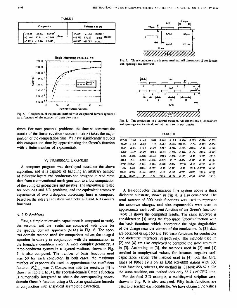
1448 IEEE TRANSACTIONS ON MICROWAVE THEORY AND TECHNIQUES, VOL. 42. NO. 8, AUGUST 1994
TABLE I
Compuumoa
141.38 -21.493 --0.9924]-21.49l 92+951 _17.844 i(pF/m)
--0.9023 -17.844 87.495 J
Del_ee ettl+ 14]
[142.09 -21.765 --0.8920"]
-18 098_ (pF/m)-21.733 93.529 +
L-_89OO -18.097 87.962
Single Microstrip (w/h=l,tr=4)
770 I0 ..... T " '+
7611 10" "................................................................ = _ ......
766 I0"z .......................-- ............................
76,jo+_ __762 l0 +z ..........
++_:o........ /._ ......................... ............
7,58 10 _ ..... / ..................................................................
75610 "2 I , i , , , J , ' i i , ,
20 40 60 80 100
Number of Basis Functions
Fig. 6. Comparison of the present method with the spectral domain approach
asa funcuonof the numberof basisfunctions.
times. For most pract!cal problems, the time to construct the
matrix of the linear equation (moment matrix) takes the major
portion of the computation time. We have significantly reduced
this computation time by approximating the Green's function
with a finite number of exponentials.
V. NUMERICAL EXAMPLES
A computer program was developed based on the above
algorithm, and it is capable of handling an arbitrary number
of dielectric layers and conductors and designed to read mesh
data from a conventional mesh generator to allow computation
of the complex geometries and meshes. The algorithm is tested
for both 2-D and 3-D problems, and the equivalent crossover
capacitance of two orthogonal microstrip lines is computed
based on the integral equation with both 2-D and 3-D Green'sfunctions.
A. 2-D Problems
First, a simple microstrip capacitance is computed to verifythe method, and the results are compared with those for
the spectral domain approach (SDA) in Fig. 6. The spec-tral domain method used for comparison solves the integral
equation iteratively in conjunction with the minimization in
the boundary condition error. A more complex geometry, a
three-conductor system in a layered medium, shown in Fig.
7, is also computed. The number of basis functions usedwas 50 for each conductor. In both cases, the maximum
number of exponentials used to approximate the coefficient
function K_,,,_ was 7. Comparison with the results in [4] isshown in Table I. In [4], the spectral-domain Green's function
is numerically integrated to obtain the corresponding space-domain Green's function using a Gaussian quadrature formula
in conjunction with analytical asymptotic extraction.
'?,+:+" +°IFig. 7. Three conductors in a layered medium. All dimensions of conductors
and spacings are identical.
2
6 7 8 9t_ ].s
r---1 1"7 r-'-i v-l r--n 'I 2 3 4 5
6 9 12 1560(3
f.r= 11
Fig. 8. Ten conductors in a layered medium. All dimensions of conductors
and spacings are identical, and all units are in micrometer.
TABLE H
307.13 -41.2 -II.34 -6.28 -5351 -218.8 4.966 -1.385 -0.814 -0.729
-41.20 319.6 -28.04 -7.79 -4.987 -5.025 -216.95 -3.54 -0.985 -0.666
-11.34 -28.04 310.5 -24.29 -8.587 -1366 -3.503 -21g.4 -3.18 -1.148
-6.279 -7.79 -24.29 303.5 -24.73 41.798 -0.946 -3.164 -219.4 -3..M5
-5.351 -4.988 -8.588 -24.73 290.5 -0.708 -0.627 -l.12 -3.325 -221.3
-218.8 -5.01 -1.363 -0.796 -0.709 231.7 -2.074 -0.393 42.182 4).134
-4.954 -216.97 -3.494 -0.944 -0.628 -2.074 232.0 -1.19 -0.255 -0.135
-1.382 -3.532 -218.4 -3.157 -1.12 -0.393 -1.19 231.8 -0.8752 -0.242
-0.813 -0.982 -3.174 -219.5 -3.32 -0.182 -0.255 -0.875 231.6 -0.763
-0.729 -0.665 -1.145 -3.34 -221.4 -0.134 -0.135 43.242 -0.763 231.3
A ten-conductor transmission line system above a thick
dielectric substrate, shown in Fig. 8, is also considered. The
total number of 300 basis functions was used to represent
the unknown charges, and nine exponentials were used to
approximate each coefficient function of the Green's function.
Table II shows the computed results. The same structure is
considered in [3] using the free-space Green's function with
the basis functions which incorporate the edge singularities
of the charge near the comers of the conductors. In [3], data
are obtained using 160 and 190 basis functions for conductors
and dielectric interfaces, respectively. The methods used in
[2] and [4] are also employed to compute the same structure
in [3]. According to [3], the methods used in [2] and [4]
resulted in nonphysical values, for instance, negative self-
capacitance values. The method used in [4] took the CPU
times of 89611.19 s on an IBM RS-6000 station with 300
basis functions, whereas, the method in [3] took 458.67 s. On
the same machine, our method took only 85.7 s of CPU time.
For the final 2-D example, a multilayered stripline case,
shown in Fig. 9, is also analyzed. Fifty basis functions areused to discretize each conductor. We have obtained the values
¢-,
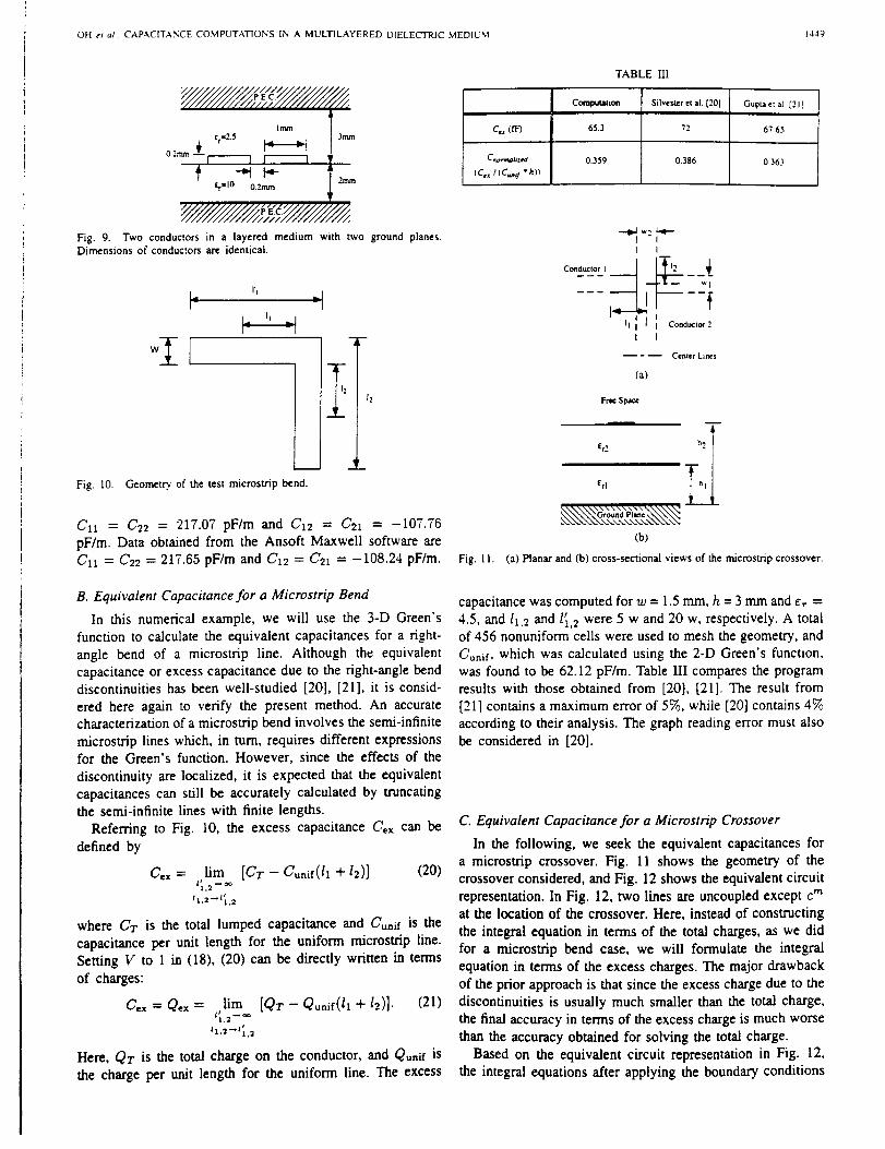
OH et al: CAPACITANCE COMPUTATIONS IN A MULT]LAYERED DIELECTRIC MEDIUM 1449
Almm
i ¢r'2"5 _"_''"-'_1 3ram
£t_ I0 0 2ram
Fig. 9. Two conductors in a layered medium with two ground planes.
Dimensions of conductorsare identical.
1
Fig. 10. Geometry. of the test microstrip bend.
-I-
i t?1'2
!
__t
Cll = C22 = 217.07 pF/m and Cz2 = C2z = -107.76
pF/m. Data obtained from the Ansoft Maxwell software areCn = C22 = 217.65 pF/m and Cz2 = Cuz = -108.24 pF/m.
B. Equivalent Capacitance for a Microstrip Bend
In this numerical example, we will use the 3-D Green's
function to calculate the equivalent capacitances for a right-
angle bend of a microstrip line. Although the equivalent
capacitance or excess capacitance due to the right-angle benddiscontinuities has been well-studied [20], [21], it is consid-
ered here again to verify the present method. An accurate
characterization of a microstrip bend involves the semi-infinite
microstrip lines which, in turn, requires different expressionsfor the Green's function. However, since the effects of the
discontinuity are localized, it is expected that the equivalent
capacitances can still be accurately calculated by truncatingthe semi-infinite lines with finite lengths.
Referring to Fig. 10, the excess capacitance C,x can be
defined by
C,x = lim [GT -- Cunif(ll W 12)] (20)
11+2_1t1,2
where CT is the total lumped capacitance and Cunir is the
capacitance per unit length for the uniform microstrip line.Setting V to 1 in (18), (20) can be directly written in terms
of charges:
C,_ = Qex = lira [Qr -- Qunif(ll "1" /2)]- (21)
/1,2_|_,2
Here, Qr is the total charge on the conductor, and Quail" is
the charge per unit length for the uniform line. The excess
TABLE HI
C_rlpuUlhon Silvester et al [201
Cu (fF) 65.3 72
C,,,,.,_l,z,a 0.359 0.386 0.363
(Cex IIC_I / *h)l
Guptaet al [21]
67.65
Conductor 1
.-.._ w2 _---
1.4.---
II
I
I
--2_I
I I Conduclor 2
1
Center Lines
Er2
frl
\N\\\\\\\
(b)
Fig. l I. (a) Planar and (b) cross-section_ views of the microstrip crossover.
capacitance was computed for w = 1.5 ram,h = 3 mm and _,. =
4.5, and lz,2 and l_,2 were 5 w and 20 w, respectively. A totalof 456 nonuniform cells were used to mesh the geometry, and
Cunil", which was calculated using the 2-D Green's function,
was found to be 62.12 pF/m. Table III compares the program
results with those obtained from [20], [21]. The result from
[21] contains a maximum error of 5%, while [20] contains 4%
according to their analysis. The graph reading error must also
be considered in [20].
C. Equivalent Capacitance for a Microstrip Crossover
In the following, we seek the equivalent capacitances for
a microstrip crossover. Fig. 11 shows the geometry of the
crossover considered, and Fig. 12 shows the equivalent circuit
representation. In Fig. 12, two lines are uncoupled except c m
at the location of the crossover. Here, instead of constructing
the integral equation in terms of the total charges, as we did
for a microstrip bend case, we will formulate the integral
equation in terms of the excess charges. The major drawback
of the prior approach is that since the excess charge due to the
discontinuities is usually much smaller than the total charge,
the final accuracy in terms of the excess charge is much worse
than the accuracy obtained for solving the total charge.
Based on the equivalent circuit representation in Fig. 12,
the integral equations after applying the boundary conditions

1450 IEEE TRANSACTIONS ON MICROWAVE THEORY AND TECHNIQUES. VOL. 42. NO. 8, AUGUST 1994
C)_ ..t._ 0
±
Fig. 12. Equivalent circuit representation for the microstrip crossover shown
in Fig. I I.
on the surfaces of the conductors can be written as follows:
2D unif 3D ex 3D exrm,,,q,,>+ ,<,,,>+
(22a)
k/c;,_,,;,)+(a,_,,,;)j2D unif 3D ex 3D ex 1rm,,,,,,>+<c,,,,,,,)+ ,,,,)
/ i¢'22D _unif\ _L /¢u3D .ex ± /p3D ..x\ J.L \_'_22 , "/22 1 T V.,12, i/21 -r- V, J22 :,-/22/
(22b)
Here, the superscript T denotes the total quantity on the line
while the superscript unif denotes the quantity per unit lengthof an isolated line. The integrations over the Green's functions
are symbolically written by (., .), and the excitation voltage is
assumed to be 1. The subscript ij used in the Green's functions
Gij denotes that the source is located at the ith conductor,
and the boundary condition is applied at the jth conductor.
The subscript ij used in the charge density functions qijdenotes that qo is the charge density at the jth conductor with
excitation at the ith conductor. Now noting that (G_D, qunif)is equal to V, we can rewrite (22) as follows:
: L + j a,,,)[_<%,:,,,,., +3D ex 3D ex "
Since the excess charges are expected to be localized, we
can truncate the domain of the basis functions used to expand
the excess charge density over distances ll and 12 from the
crossover junction (see Fig. 11(a)). Now using pulse basis
functions and the point matching technique, (23) can be put
into the following matrix form:
,:V22 t'm [M2, M=_ J/ql_ q_ J
(24a)
£m
4
4
TABLE IV
_.1 = 2, and,_.2 = 2 _.1 = 4, and _2 = 2
69.17 fiF) 59.748 (t17)
-55.40 (IF) --48.580(iF)
-58.94 (IF) -53.968 (IF)
TABLE V
COMPARISON OF RESULTs FOR FIG. I1 WITH er] = _r2 = 2
Papatheodorou et al.
[ 1O] Computation
c m overhl _ 1.672 1.776
h_c, - 1.345 - 1.321
-I.296" -1.513
* This entry is incorrect, and it can be verified b_' considerin_ J l0, Fi_. 4].
where
t
[Vu]b = - J¢i Gf_(pi I p')dl'
= - f_, G,2 (P, I p')dl' (24b)[V=2]ij 2D
Mklij = is Sj aPkD (I"i I rl)d,.q# (2*)
[ ]'q_X = ex ex exqij,1, qij,2, " • ", qij,.%'a_.,
q_nlf [ unif unif unif ] ¢= qii,2 ,''' qii,.'V2D.i[qii,1, , . (24d)
Here, [A]o is the jth element of the ith row of the matrix A,
and NaD,i and N2D,i are the number of patches and the numberof segments used to discretize the surface and the cross section
of the ith conductor, respectively, q_nif can be obtained by
solving the 2-D problems for each isolated microstrip with the
excitation voltage set equal to 1. Then (24) can be solved for
the excess charges. Finally the equivalent excess capacitancecan be found by
c_ = _ Areai_" qi_kk----'l
(25)
where Areaik is the area of the kth patch in the ith conductor.
For a numerical example, the same structure used in [10] is
considered, where hi and h_ were 4 mm and 6 mm, the widths
of both strips were 0.04 hi, respectively, ll and 12 were 10
h_, and 800 nonuniform patches and 40 pulse basis functions
are used to solve the 2-D and 3-D problems, accordingly.
Two different dielectric configurations are considered and theresults are shown in Table IV. The maximum number of
exponentials used for each coefficient function was seven for%

OH et _:.: CAPACITANCE COMPUTATIONS IN A MULTILAYERED DIELECTRIC MEDIUM 145t
2 0xl0 l't_L 20
,o,,o.- "'0 ,-00_ 00(I
-005 000 0.05
x x
2
Y 0
20 _ 0.05
005 -005 000 -0.05 000It x
(a) (b) (c) (d)
Fig. 13. Plots of the magnitudes of the excessive charge distributions for (a) qll,t" (b) q2t,_z (c) qt2"et and (d) q22_z with erz = 4. and t,2 = ..'_ x and
> denote the transverse and the longitudinal, respectively.
both cases. The result with e,1 = e,2 = 2 are compared
with the results from [10] in Table V. In Table V, c_ and c_
are the capacitances per unit length of the isolated wire lineswith radii equal to 0.25 w and e,1 = e,-2 = 1. In [10], ll
and 12 were 10 hi; hence, their value of c m is expected to
be smaller than ours as shown in Table V. The 3-D plots of
excess charges are shown in Fig. 13. The Green's function usedin [10] is based on the image principle in the space domain
and involves an infinite summation. According to [10], only
ten terms were sufficient to evaluate the infinite summation
for this particular structure, where lines are extremely narrow.However, for wider microstrip lines, the number of terms to
compute the infinite summation will be much larger; this can
be easily seen from the expression of the Green's function in
[10].
VI. CONCLUSION AND FUTURE WORK
In the design of VLSI circuits, the capacitance computation
plays an important role, and the present method can be
conveniently combined with CAD tools. Since the Green's
function depends only on the processing parameters, such asthe thickness and number of dielectric layers, the dielectric
constants, and location of ground planes, the Green's function
approximation has to be performed only when the processing
parameters are changed. Then, the approximation result can
be used to compute capacitance parameters throughout the
design period.In the computation of parasitic or excess capacitances, semi-
infinite microstrip lines are often encountered, and to haveaccurate results, as mentioned earlier, the integral equation
is often formulated in terms of the excessive charges which,
in turn, requires the Green's function due to the semi-infinitelines. The authors are currently studying the generalization of
the present method for such a Green's function in a layered
medium.
APPENDIX A
THE REAL-VALUED EXI_NENTLM. APPROXIMATION
BASED ON THE RELAXATION OF CURVE FTITING
First,we willassume thata functiony(x) to be approxi-
mated isrealvaluedand nonoscillatoryand,furthermore,that
itsasymptoticvalueiszero.The latterassumptioncan easily
be satisfiedifthefunctionislimitedatinfinity.Our goalisto
find the right-hand side of
y(x) _ A(x) = _ fi(x) = A--,,=I 'i=l
(AI)
Let w us for a moment assume that each first-order function fi
approximates the original function y at some interval around
one of the approximation points and is decreasing fast enough
so that its value is negligibly small at the approximation points
corresponding to larger values of the argument x. Then, we
can safely determine one of the first-order functions, say fl, by
neglecting contributions due to the other first-order functions,
which are as yet unknowns to be determined. The parameters
of fl can be easily obtained by curve fitting two values of y
for some large value of x. In a similar manner, we can find
the parameters of the other first-order functions; however, thistime we have to take into account contributions due to the
previous ones which are already known.
From the above argument, given 2N approximation points,
the equations used to determine the parameters for the ith
first-order function are then written by
Ai = 2r In (yi(2X2i_l)/Yi(X2i)) (A2)X2i -- X2i_ 1
Ci = e-'X'x2'-_yi(x2i-1) (A3)
where
yi(xj) = yi-l(xj)- fi-l(xj); j = 1,...,2N. (A4)
In the above, yo(Xj) is equal to y(x./). Let us now considerthe case in which the value of a first-order function is not
negligible at the other approximation points. In this case, if we
perform the above procedure, there will be some difference
between the original and the approximated function since
we have ignored contributions due to some of the first-orderfunctions. In such a case, to reduce this difference, we can
iterate the above procedure including the contributions due toall other first-order functions which were obtained from the
previous iteration. Thus, for the kth iteration, (A4) must bemodified as
i-1 N
1=1 1=i+1
j = 1,...,2N. (A5)

1452 IEEE TRANSACTIONS ON MICROWAVE THEORY AND TECHNIQUES. VOL 42, NO. 8. AUGUST 1994
I
01
0.01
oool
¢-2,1
..... I-.... I........................................... O" * Ilia It_ ---
----_- - _4 J_.
I 2 3 4
x
(a)
Finally, to demonstrate the method, the following testing
function is approximated and the results are shown in Fig. 14:
_-2x
y(x) = _ + e -=. (A6)v"i + z
As illustrated in Fig. 14(b), to find the exact location of the
pole at -1, we need a large number of iterations; however,
since our goal is to approximate the overall function, only afew iterations were needed to approximate the function. To
locate the poles exactly, one should use other methods such as
those based on pencil of functions or the Prony approximation.
APPENDIX B
Locationof Pole vs. # of Iterations" 1.05 " 1 7 _ r 7 " d r _ r " " _ r r i '
t_ -I.07
.__
-I.09
-1,1
-I.II
-IA2 ' J ' ' ' ' '
2 4 6 8 10 12
Number of Itenltions
Co)
Fig. 14. (a) Comparison of approximated and exact values of (A6). (b)Convergence of the location of the smallest pole (-1) with the number ofiterations.
It can easily be shown that if y(x) had N distinct eigen-values, by iterating the above procedure, the approximated
function will converge to the original function. However, in
general, the approximating function will never be exact and
the iteration must be stopped at some point at which the
approximated function is optimal in the sense of curve fitting.
Since our curve-fitting algorithm, most likely, has the biggest
relative error for the values of x between X2N_ 1 and x2.,_', one
can check the approximated value with the exact value at any
point in this interval for the convergence criterion. In some
cases, if the desired accuracy can not be achieved, then one
should increase the number of exponentials. This case can be
determined by checking the difference between the computed
parameters of fi (k) and f(_-l).
The described method allows one to find the parameters of
an approximating function one-by-one directly without solving
a system of nonlinear or linear equations and does not require
an original function to be monotonic. Moreover, the limiting
values of the approximated function match exactly with the
original function.
STRIP TRANSMISSION LLNE CASE
Solving Poisson's equation with separation of variables,
the Green's function for the strip transmission line case with
the distance h between two ground planes can be written asfollows (see [22]):
±_c
afx.ylx'.V) : _ lsin (nr, y)7rE n \ h /
rt_l
-- . (A7)
The above expression for the Green's function can be easily
integrated analytically over the pulse basis function analyti-cally. This summation is quickly converging, and only a few
first terms are needed; for instance, four digits of accuracy can
be obtained using less than five terms for Ix - x'l/h > 0.5.
However, when Ix - x'l/h is small, the summation converges
rather slowly, and the use of this Green's function expression
should be avoided. In such cases, we can use the followingclosed-form Green's function:
1
G(x, y Ix', y') = _ In
(A8)
This expression for the Green's function can be obtained using
the conformal mapping and the method of images [18]. Themajor disadvantage of this expression is that the closed-form
integration over the pulse basis function is unappealing; hence,the numerical integration scheme is unavoidable. Therefore,
this form of the Green's function must be only used when
Ix- z'l/h is small. As shown in [1], to integrate (A7)
numerically, it is convenient to rewrite this expression byextracting the singularity as
= _leln[(x - x'):+ (y - y')_]G(x,y Ix',V)
+ g(x. y I x', y') (A9)
g(z, y fx',y') = _-leln[(x-x')2+(y-Y')2][ sinh_[_=2-_][_(_-=')] +sin2 [_]]]
sinh_L 2h J +sin2 [_]
(A 10)

Oil et al' CAPACITANCE COMPUTATIONS IN A MULTILAYERED DIELECTRIC ,_,IEDII_'M }aS3
where ¢A lO), shown at the bottom of the previous page.Now
the first term in (A8) can be analytically integrated using
(20(b)), and the second term can be integrated numerically.
ACKNOWLEDGMENT
The authors gratefully acknowledge Professor R. Mittra
for encouraging this work and helpful suggestions. Drs. M.
1. Aksun and P. Harms are also acknowledged for helpful
discussions.
REFERENCES
[1] W. T. Weeks, "'Calculation of coefficients of capacitance of multicon-
ductor transmission lines in the presence of a dielectric interface," IEEE
Trans. Microwave Theory Tech,, vol. MTT-18, pp. 35-.43, Jan. 1970.[21 C. Wei, R. F. Hamngton, J. R. Mautz. and T. K. Sarkar, "'Multicon-
ductor transmission lines in multilayered dielectric media," IEEE Trans.
Microwave Theory Tech., vol. MTT-32, pp. 439-.450, Apr. 1984.[3] G. W. Pan, G, Wang, and B, K. Gilbert, "Edge effect enforced bound-
ary element analysis of multilayered transmission lines," IEEE Trans.
Circuits Syst., vol. 39, pp. 955-963. Nov. 1992.
[41 W. Delbare and D. D. Zutter, "Space-domain Green's function approach
to the capacitance calculation of multiconductor lines in multilayered
dielectrics with improved surface charge modeling," IEEE Trans. Mi.
crowave Theory Tech., vol. 37, pp. 1562-1568. Oct. 1989.[5] E. Yamashita. "'Variational method for the analysis of microstrip-like
transmission lines." IEEE Trans. Microwave Theor?," Tech.. vol. M'l'r-16,
pp. 529-535, May 1964.[6] H. A. Wheeler, "'Transmassion line properties of parallel wide strips by
a conformal mapping approximation." IEEE Trans. Micro_vave Theor)'
Tech., vol. M'r'T-12, pp. 280--289, May 1964.[7] J. Svacina, "'Analysis of multilayer microstrip lines by a conformal
mapping method," IEEE Trans. Microwave Theory Tech., vol. 40, pp.
769-772, Apr. 1992.[8] A. Farrar and A. T. Adams, "Multilayer microstrip transmission lines,"
IEEE Trans. Microwave Theory. Tech.. vol. M'I'T-12, pp. 889-891, Oct.1974.
[9] W. E. Matzke, B. Heinemann. and R. Telschow. "On the calculation of
the capacitance coefficients for VLSI multilevel metallization lines by
using domain methods," IEEE Trans. Electron. Devices, vol. ED-36, pp.
4_.7.---M9. Feb. 1989.
[10] S. Papatheodorou. R. F. Harrington, and J. R. Mautz, "The equivalent
circuit of a microstrip crossover in a dielectric substrate.'" IEEE Trans.Microwave Theol. Tech., vol. 38, pp. 135-140. Feb, 1990.
[I 1] H. Nelis. E. Deprettere, and P. Dewilde, "An efficient method for mod-
elling VLSI interconnections," European Con( Circuit Theo_ Design,
Sept. 1989, pp. 94-95,[t2] W. Veit, H. Diestet and R. Pregla. "Coupling of crossed planar multi-
conductor systems," IEEE Trans. Microwave Theory Tech., vol. 38, pp.
265-269, Mar, 1990.
[131 A. H. Zemanian, R. P. Tewarson. C. P. Ju, and J. F. Jen, "Three-
dimensional capacitance computations for VLSI/ULSI intercon-
nections," IEEE Trans. Computer-Aided Design, vol. CAD-g, pp.1319-1326, Dec. 1989.
[ 14,1 M.I. Aksun and R. Mittra, "Derivation of closed-form Green's functions
for a general microstrip geometry," IEEE Trans. Microwave Theory
Tech., vol. 40, pp. 2055-2062, Nov. 1992.[15] Y. L. Chow, J. J. "fang, and G. E. Howard, "Complex images for
electrostatic field computation in multilayered media." IEEE Trans.
Microwave Theory Tech., vol. 39, pp, 1120-1125, July 1991.116] S. L. Marple, Digital Spectral Analysis. Englewood Cliffs, NJ:
Prentice-Hall, 1987.
[17] Y. Hua and T. K. Sarkar, "Generalized pencil-of-function method for
extracting poles of an EM system from its transient response," IEEE
Trans. Antennas Propagat., vol. 37, pp. 229-234, Feb. 1989.
[181 P. M. Morse. Methods of Theoretical Physics. vol. 2. New York:McGraw-Hill. 1953.
[191 D. R. Wilton, S. M. Rao. A. W. Glisson. D. H. Schaubert. O. M.
AI-Bandak et al.. "'Potential integrals for uniform and linear source dis-
tributions on poi)gun and polyhedral donlaim,,'" IEEE Tr,,_a. ,.t,Jtut_tlas
Propagat., vol. AP-32. pp. 276-281, Mar. 1984.
[201 P. Silvcster and P. Bendedek. "Correction to 'Microstrip discontinuitycapacitances for right-angle bends, T junctions, and crossings'," IEEE
Trans. Microware Theory Tech. vol. M"I'T-23, p. 456, .M_y 1975.
[211 K. C. Gupta. R. Gary., and R. Chadha. Computed.Aided Design ofMicrowave Circuits. Norwood. MA: Artech House, 1987.
[221 R. E. Collin. Field Theory of Guided Waves. 2nd ed. New York: tEEE.1991.
Kyung S. Oh (S'91) was born in Pusan, SouthKorea, in 1965. He received the B.S. and M.S.
degrees in electrical engineering from the University
of illinois. Champaign in 1990 and 1992, respec-
tively. He is presently studying in the Graduate
School of Electrical Engineering at the University
of Illinois. where he has been engaged in research
on modeling and simultation of high speed digitalcircuits.
Dmitri B. Kuznetsov was born June 26, ]966,
in Moscow, U.S.S.R. He received the Dipl. Eng.in electronics engineering from the Moscow Elec-
trotechnical Institute of Telecommunication, Depart-ment of Automatics, Telemechanics and Electronics,
in 1988. He received the M.S. degree in electrical
and computer engineering from the University. of
Illinois, Champaign in 1993, where he is pursuing
the Ph.D. degree.From 1987 to 1991, he worked as an electronics
engineer at the Space Research Institute. Academy
of Sciences of the U.S.S.R.. Moscow, on the design, manufacturing, testing,
maintenance and repair of computer graphics system. From 1988 to 1991, heattended the postgraduate school of the Space Research Institute specializing
in the information and measuring systems in space research.
Jose E. Schutt-Aine (M'82) received the B.S. de-
gree from Massachusetts Institute of Technology.
Cambridge, and the M.S. and Ph.D. degrees from
the University of Illinois in 1984 and 1988. respec-
tively.
Following his graduation from MIT, he spent two
years with Hewlett-Packard Microwave TechnologyCenter in Santa Rosa, CA, where he worked as
a device application engineer. While pusuing his
graduate studies at the University of Illinois, he
held summer positions at GTE Network Systems
in Northlake, IU He is presently serving on the faculty of the Department of
Electrical and Computer Engineering at the University of Illinois an Assistant
Professor. His research interests include microwave theory and measurements,
electromagetics, high-speed digital circuits, solid-state electronics, circuit
design and electronic packaging.

IIEE FRANSAtTI()N _, ()N MICR()_A'_E THEORY AND TECHNIQU[-S. ',()L 44 NO 2. t-EBRLAR'_ I'b_*_ _47
Computation of the Equivalent Capacitance
of a Via in a Multilayered Board Using
the Closed-Form Green's Function
K,,ung S. ()h. Jose E. Schutt-Aine. Raj Mittra. and Bu Wang
Abstract--A method based on the quasi-static approximation for
computinR the equivalent capacitance of a via is presented in this paper.The geometry of a via consists of traces, pads and a perfectly conductingcylindrical rod: the via is buried in a multilayered dielectric medium withoptional relerence Iground) planes. The total number of traces, pads. andground planes can be arbitrary, as well as the angles and cross sections.The method is based on the excess charge formulation of an integralequation applied in conjunction with the recently developed closed-formGreen's function.
I. INTRODUCTION
Although a via is one of the most common discontinuities en-
countered in high-speed integrated circuits, it has not received asmuch attention as _ome of the other discontinuities, e.g.. open-
end terminations, bends, and junctions. This is due mainly to the
nonplanar and complex three-dimensional (3-D) geometry of the via.which has often been simplified in the works published previously
[I]-[31. For instance, a via penetrating through a single relerence
(ground) plane with two wire traces has been considered in [1],and without any traces in [2]. while a via above a reference plane
with two wire traces but without a through-hole reference plane
between these trace_, has been investigated in 13]. A novel equivalent
network model, which accounts for the frequency dependence, has
been proposed in 141 and has also been applied to the problem
of coupling between two adjacent vias in [5]. in [11 and [31, an
integral equation has been formulated in terms of the excess chargedistribution to compute the equivalent (excess) capacitance. In this
paper, this excess charge formulation is further generalized for vias
with more complex geometries than has been analyzed hitherto and
is applied in conjunction with the closed-form Green's function to
analyze vias embedded in multilayered dielectric media.
A closed-form Green's function for a multilayered dielectric
medium was first introduced in 16]. This Green's function utilizes
a finite number of complex images and avoids the evaluation of a
nested tntinite series expression required in the computation of the
exact Greens function for a layered medium. In [7], a closed-form
Green's function based on weighted real images was proposed and
was used to compute the equivalent circuit of a stop crossover. In
[8]. this closed-form Green's function based on weighted real images
was further generalized to handle a semi-infinite line and then applied
to compute various strip junction discontinuities. In this paper, the
closed-form Green's function discussed in 18] is employed to compute
the equivalent circuit for a via in a multilayered dielecmc medium.
!1. GENERAL STATEMENT OF THE PROBLEM
To illustrate the geometries of vias considered in this paper, a via
comprised of three traces and one reference ground plane is shown in
Fig. I(a). In general, a via can pass through Ng reference (ground)
planes and YG traces, and .Vp pads can be attached to the via where
Manuscript received April 10. 1995: revised November 12. 1995.The authors are with the Department of Electrical and Computer Engi-
neering. Electromagnetic Communication Laboratory, University of Illinois.Urbana. IL 61801-2991 USA.
Publisher Item Identifier S 0018-9480(96)01461-5.
Trace I
Pad I
Reference Conductor I
12
Trace 2
Pad 4
Pad 3 Y_13 z
(a)
Trace3
. ,::'. _='dNd
Y---dNa-I
,','-k:'":"
i?iiiiii!iii?iiiiiiii?!iii!iiiiiiL :,. !iiiiiiiiiiiiiii!i!!?!ii!i'iiii!i.,,,,,,,,,,,,, .... ,,,,,,,,,,,,,,,,,,, ,,,, y=d I::::::::::::::::::::::::::::::::::::: i:!:!:
y=,a
Y
(b)
Fig. I. (a) The geometry of a via. and (b) its surrounding muhilayeredmedium.
N_. N,, and N_, are all arbitrary. The vias are embedded in a multi-
layered medium consisting of 3"_ (arbitrary) dielectric layers, which
can be backed by two optional reference planes as shown in Fig. lib).
To distinguish between these optional reference planes and those
associated with the via. we will reserve the term "'reference plane" to
designate an optional top or bottom reference plane, and use the term"reference conductor" to denote other reference planes. It is evident
that the reference conductors must have perforations to avoid any
contact with the vias: however, the two optional reference planes are
assumed to be solid. To simplify the numerical computation, we as-
sume that all of the conductors are infinitely thin and that the shapes of
all the pads and perforations in the reference conductors are circular.
A quasi-static equivalent circuit representation of the via shown in
Fig. I is given in Fig. 2. This paper will only address the problem
of computing the total equivalent capacitance C,. The method to
compute the equivalent inductance of a via can be found in [9].
In ,Section Ill. an integral equation is formulated in terms of the
excess charge distribution using the closed-form Green's function,
and the method of moments (MoM) is subsequently employed to
determine the unknown charge distribution. A detail discussion of
the closed-form Green's function and the corresponding expressioncan be found in [8]. In Section IV. several numerical examples are
presented to verify the proposed method.
II!. FORMULATION OF AN INTEGRAL EQUATION
An impressed potential on conductors results in free charge accu-mulation on the surfaces of conductors, and the electrostatic potential
0018-9480/96505.00 © 1996 IEEE

_4N IEEE TRANSACTIONS ON MICROWAVE THEORY AND TECHNIQUES. _OL 44 NO 2. FEBRUAR'I 1'49_
TABLE 1
EQUIVALENT CAPACITANCES FOR ViAS SHOWN IN FiG 3. UNITS ARE Jr; pF
Computed Result
Others
EI=E2=£ o
0.3841
0.3701 [31
Fig, 3(a)
¢1=4 co, _'.'_ G,
1.233
t.28 [31
Fig. 3(b)
E/=_-,--_4G, ,f/=4 5 E,.,,.£2=5.4£o
II
9.952 12.3 I
635 Ill 7.85 Ill
Fig. 2.
0
12
v I
L,.z2e/_ 0
'T"
ce,3
A equivalent circuit representation of the via shown in Fig. I(a).
o(r) at any point except inside conductors is then related to this
surface charge density q(r) via the following integral equation
o(r)=.f_G:_r)(r I r'lq(r')dr' = (GaD.q) (1)
where £._ denotes the surfaces of all conductors, including the via
and reference conductors. G:+D(r I r') is the 3-D closed-form Green's
function for a multilayered medium, and it accounts for polarization
charges on dielectric interfaces and free charges on the surfaces of
reference planes [8]. The integration is symbolically written as (...)
to simplify the notation. Next. the charge distribution over the whole
structure analyzed is decomposed into q,. (r ). q'o (r ). q_ (r ). and _ti_lr /
where q,4 r! is the charge density on the surface of a via hole. and
%( r _. ,1;( r L and q',(r) are the charge densities on the ith pad. trace.
and reference conductor, respectively. Equation (I) can be rewritten
as
.N p
o+,.)= +_c,,"'+".,.,,,) + _(c,:".,+,;,)
,Xp \a
+ _<c,"'". _;>+ _<a:'" ,j;>. (2)_-----I l=t
Next. the charge density ql (r ) is further decomposed into the uniform
charge density q,,.,,t,tr) and the excess charge density q't......... (r)
q;(r) = ql `"'l '(r) + q', "'" .... (r}. (3)
Here. ,li'"'l'(r ") is the uniform cha_e density on the ith trace
under the assumptions that it is infinite in both directions, no other
traces are present, and the reference conductors have no perforations:
this charge density is computed by solving an appropriate two-
dimensional (2-D) problem. Since the reference conductors become
uniform planes without any perforations for this 2-D problem, the
potential distribution on the region above the reference conductor
is not affected bv the region below it and vice versa. To solve
for ,f"" 'qrL it is then expedient to introduce a new medium
surrounding the _th trace. As a consequence, the medium employed
in the 2-D problem is generally different from that of the 3-D via
problem, and could, in fact. be different for each trace. Once the
appropriate medium has been chosen. ,/i'"t '!,'1 can be obtained by
using the method described in [7]. The resulting ,J_'"'f'lr) yields
the capacitance per unit length for the ith transmission line in the
equivalent circuit representation shown in Fig. 2.
In the process of determining 91'"'"'(r). the 2-D closed-form
Green's function G_t)'(p I po) is used to formulate an integral
equation for a 2-D problem |7]. However. in the integral t2) for
computing the equivalent capacitance problem, the uniform chargedensity qi'"d'lr) resides on the ith trace, which is only a semi-
infinite line. It is therefore necessarv to employ G _''' .... <,' I r.. _1
to compute the potential due to 9_'"':'(r) [8]. Using (3). (2) can be
rewritten as
o(r)- _V,(G....... .q:"'>
.%'p
= <G_._, ) + Z(a_').q;)
.'v¢ '\'9
+ _<c, :+°.,j; ....... >+ _<a +_. q;>. (+),=1 I=l
If we set the via potential to be oo with respect to the reference
conductors and planes, o(,') becomes oo on the surfaces of the via
hole. pads. and traces, and is equal to 0 on the surfaces of reference
conductors. Hence. once qi'"'_'(r) has been determined, all of the
quantities associated with the left-hand side of (41 can be considered
to be known at the sunhce of the conductors, and the method
of moments can be applied to solve <4). The various integrations
appearing in (4) can be evaluated analytically for pulse-type basis
functions using closed-form formulas given in [8].
Once the unknown charge distributions have been determined, the
equivalent (excess) capacitance C, can be obtained by using the
following expression which involves the integrals of these charge
distributions
.\'p
-X t \ v
+ q'," ...... r'),h" + 'l,,t ),it' (5)+_ r., -- _,
where O-,. is the surface of a via hole. _._p,. ';.),.,. and _.)+,, and are the
surfaces of the ith pad. trace, and reference conductor, respecttvel>.
IV, NUMERICAL EXAMPLES
We will now present two numerical examples to illustrate the
application of the method presented above to the computation of the
equivalent capacitances of two via structures, one with a reference
plane and the other with a reference conductor. The detailed geome-
tries of the two via structures are shown in Fig. 3. The computed

lEEk IR.\3,_,_\( ll()\'_ ()x MI( R(]_,A_,E THEORY AND TECHNIQLES \()L -_-i x,() 2 F-EBR{ \R'_ I')q6 'a'_
8.02
80
40
(a)
50
4.02
4.02
50
4
(b)
Fig. 3. (a) A two-trace via with a reference plane and (b) a two-trace viawith a reference conductor. All dimensions are in mm.
applicable to ,,la geometries with or without lhrough-hole relerence
conductors. The recently developed closed-lotto Green's, luncuon _as
employed to circumvent the time-consummg evaluation of a nested
inhmte _,eries. required tn the evaluation 131.
REFERENCES
l I] T. Wang, R. F Harrmgton. and J R. Mautz. "Quasl-qatic anal_.',_,, t}l a
mlcrostnp via through a hole in a ground plane," IEEE Trans. Mi(ro_m'eTheory Tech.. ',ol. 36. pp. IO08-1013. June 1988.
[2] P. Kok and D. De Zuner. "Capacitance ol a circular symmetric modelof a via hole including finite ground plane thickness," IEEE Tranr.
Microwave Theory Tech.. vol. 39. pp. 1229-1234. July 1991.
[3] T. Wang, J. R. Mautz. and R. F. Hamngton. "'The excess capacitance t)f
a microstnp via in a dielectnc substrate." IEEE Tr, ns. Computed.A/ded
Desten, vol. 9. pp. 48-56. Jan. 1990.
[41 Q Gu. Y. E. Yang. and M. A. Tassoudji. "'Modeling and analy,_ls ofvias in multilayered integrated circuits,'" IEEE Trans. Microwave Theory'
Tech., vol. 41. pp. 206-214. Feb. 1993.
151 Q. Gu, M A. Tassoudji. S. Y. Poh. R. T. Shin. and J. A. Kong. "'Coupled
noi.,,e analysi,s for adjacent vms in multilayercd digital clrcmts." IEEE
Tran,_. ('ircutt Sv,_t.. ",ol. 41. pp. 796-804. Dec. 1994.
161 Y. L. Chow. J. J, Yang. and G. E. Howard. "'Complex image,,, lor
electrostatic field computation m multilayered media." IEEE Trans.Microwave Theory Tech.. vol. 40. pp. 1120-1125, July 1991
17] K. S. Oh. D. Kuznetsov. and J. E. Schun-Ain¢. "Capacitance compu-tations in a multdayered dielectric medium u_lng closed-lotto ',patrol
Green's funcnons.'" IEEE Trans. Microwave Theory Tech.. ,,ol. 42,
pp. 1443-1453. Aug. 1994.[8] K S. Oh. "Efficient modeling of interconnecuons and capacmve dis-
continuities in high-speed digital circuits," Ph.D. dissertation. Univ of
IL at Urbana-Champaign. 1995.
[91 A. R. Djordjevic and T. K. Sarkar. "'Computation of inductance of
simple vias between two striplines above a ground plane." IEEE Trans.Microwave Theory Tech.. s'ol. 33. pp. 265-269. Mar. 1985.
Analysis of Edge Coupled Strip Inset Dielectric Guide
excess capacitances for Fig. 3(a) with I) f_ = :., = r j and 2)
-I = 4_'_j and _% = _J; for Fig. 3(b) with 3) _1 = !,_ = 4_-0 and
4) -_ = 4.5-_j and -.': = 5.4_-% are listed in Table I along with data
obtained from I1] and [31. In [11 and 131. the strips were replaced
by the equivalent wires of radii which are one-fourth of the widths
of the strips. In our computation, the lengths of all traces have been
truncated to 2.5h. whereas the width of the reference conductor has
been truncated to 1.51, with h and I being the height of a via hole
and the length of the traces. The truncation of traces and reference
conductors is valid since the excess charge distribution decays rapidly
as we move away from the center of a via. A total of 263 and
687 unknowns were used for the vias shown in Figs. 3{a) and (b),
respectively. As shown in Table I. the data for the via shown in
Fig. 3(a) agree well with the published results. However, the data
for the via shown in Fig. 3(b) are considerably different from the
results reported elsewhere. Unfortunately, no experimental result for
this structure is available to establish the relative accuracy of these
results associated with Fig. 3(b).
V. CONCLUSION
A method to compute the equivalent capacitance of a via, which
is based on an integral equation formulated in terms of the excess
charge formulation, has been presented in this paper. The method is
Z. Fan and Y. M. M. Antar
Abstraet_Tbe edge coupled strip inset dielectric guide is analyzed using
the extended spectral domain approach. This structure, as compared to
microstrip line, has several interesting features and can be very useful formicrowave and millimeter wave applications. Validity of the approach is
established by comparing numerical results with measured data. As manystructural and material parameters can be chosen, a wide fundamental
mode bandwidth and a broad range of characteristic Impedances can be
achieved, leading to great flexibility. The dispersion in fundamental mode
propagation constants and Impedances is found to be very low. With
suitable choice of different permittivities for two dielectric layers, the
same propagation constants for two fundamental modes can be obtained.
This property is desirable for directional coupler applications.
1. INTRODUCTION
Microstrip line has been the most popular transmission medium
used for constructing microwave and millimeter wave circuits [ I ]. it
is well known that one of the problems with open microstrip circuits
is the excitation of surface waves from discontinuities in the circuits
Manuscript received July 26, 1995: revised November 12, 1995.
The authors are with the Department of Electrical and Computer Engineer-
ing, Royal Military College of Canada. Kingston, ON K7K 5L0, Canada.Publisher Item Identifier S 0018-9480(96)01462-7.
0018-9480/96505.00 © 1996 IEEE

EFFICIENT TRANSIENT SIMULATION OF
DISTRIBUTED INTERCONNECTS
Jose E. Schutt-Aine and Dmitri Kuznetsov
Electrical and Computer Engineering,University of Illinois,
Urbana, IL 61801,USA
I. Introduction
The electrical performance of high-speed integrated circuits and digital networks
strongly depends on the behavior of interconnects between various components of these
systems. The prediction of such performance can only be achieved by the used of
computer-aided design and simulation tools. The simulation of high-speed digital circuits
has gained a significant role in the past few years since it is critical in the evaluation of noise
levels, signal corruption and signal delay in fast switching circuits. This paper explores the
various aspects and techniques for transmission line simulation; in particular, two different
methods are described: the scattering parameter method and the optimal method.
Two main aspects in the solution procedure must be distinguished, namely the line
model and the transient simulation scheme. In the transient simulation step, the time-
domain representation of the line model is obtained to yield the transient solution.
Two different classes of models can be employed: circuit models and non-circuit
models. Non circuit models cannot be directly implemented into a circuit simulator. Circuit
models can be directly incorporated into a circuit simulator; they relate voltages and currents
at the line terminals and are independent of the terminations.
Further, two types of line characterization can be identified, namely closed-loop and
open-loop characterizations. A closed-loop characterization such as Z- Y- H- and S-
parameter characterizations results in complex oscillating transfer functions and transient
characteristics. An open-loop characterization--in terms of the propagation functions--
separates forward and backward waves and results in simple transfer functions and transient
characteristics.
II. Scattering Parameters
Scattering parameters have been extensively used in microwave applications for the

measurementof high-frequencycircuitsaswell ascircuit analysis. Theadvantagesof the
scatteringparameterapproachresidein theflexibility in thechoiceof thereferencesystem
which can be adjusted to match certain characteristicsof the network under study and
simplify the analysisandthecomputations[1]-[3]. A direct consequenceof thispropertyis
the greatercomputationalstability andthe simplicity of the closed-formsolutions. More
specifically, losslessand lossy transmissionlines can be analyzedin conjunction with
nonlinear terminations to yield solutions in which backward and forward waves are
separated(seeFig. 1).
LossyArbitrary Nonlinear andDispersive Nonlinear ArbitrarySource Load Line Load Source
x__ x:lPort 1 Port 2
Fig. 1.
Consider a transmission line of length I with complex characteristic impedance Zc and
propagation velocity v. This transmission line is connected to two ideal lossless reference
lines as shown in Fig. 2, it can then be described in the frequency domain through its
scattering parameters using
B1 = SlxA! + Sl2A2 (la)
B2= S21AI +$22A2 (lb)
where A1 and A2 are the incident voltage waves in the reference line of characteristic
impedance Zo. B 1 and B2 are the reflected waves due to A 1 and A2 respectively. It can be
shown that
where
Sll = S22 = (1 - e-2jt°l/v)p (1 - p2)e-jt°l/v1 - e-2jc°Vvp 2 S 12 = 821 = 1 - e-2jc°l/vp 2 (2)
Zc- 7-0 (3)0 =Zc

In the time domain this correlates to (lowercase characters for time-domain variables'
bl(t) = s i l(t)*al(t) + s 12(t)*a2(t)
b2(t) = s21(t)*a l(t) + s22(t)*a2(t)
where sij(t) is the time-domain Green's function associated with Sij. These equanons
combined with the terminal conditions
(4a)
(4b)
are
al(t) = Tl(t)gl(t) + Fl(t)bl(t)
a2(t) = T2(t)g2(t) + F2(t)b2(t)
(5a)
(5b)
ReferenceLine
A1
B I
TestLine
--- x--O x=l
Fig. 2.
ReferenceLine
_ B 2
-_ A 2
where T l(t), T2(t) are the transmission coefficients, l"l(t) and F2(t) are the reflection
coefficients and gl(t) and g2(t) are the time-domain expressions for the voltage sources.
Tl(t), T2(t), Fl(t) and F2(t) are time-dependent and are related to the terminations Zl(t) and
Z2(t) of Fig. 1 which may be the time-domain representations of reactive elements or
linearized active circuits. The convolution operation is defined as
t
sij(t ) * aj(t) = fsij(t - "_)* aj (a:)d'c0 (6)
When time is discretized the convolution becomes
t
sij(t ) * aj(t) = Y.sij(t - z)aj(,)Ax"_=1
(7)
where AX is the time step.
we isolate the term containing aj(t)

t-I
Sij(t ) * aj(t) = sij(0)aj(t) + Y, sij(t - "_)aj(_:)Ax"r=l
(8)
we then define the history term as
t-I
Hij(t ) = _sij(t - I:)aj(z)A'I; •1:=1
History (9)
Define s'ij (0) =sij (0)Ax we finally obtain
bl(t) = S'll(0)al(t) + s'12(0)a2(t) + Hll(t) + H12(t) (10a)
b2(t) = s'21(0)al(t) + s'22(0)a2(t) + H21(t) + H22(t) (10b)
When combined with the termination conditions of (5), the solution for the independent
waves can be extracted to yield
al(t) = [1-F2(t)s'22(0)] [Tl(t)gl(t)+Fl(t)Ml(t)] Fi(t)s'12(0)[T2(t)g2(t)+F2(t)M2(t)] (lla)A(t) + A(t)
a2(t) = [1-Fl(t)S'll(0)] T2(t)g2(t)+F2(t)M2(t)] F2(t)s'21(t)(0)[Tl(t)gl(t)+Fl(t)Ml(t)] (llb)A(t) + A(t)
A(t ) = [ 1-F l(t)S'l 1(0)] [1- F2(t)s'22(0)] - F 1(t)s'12(0) F2(t)s'21(0) ( 11c)
with M! (t) = Hll (t) + H12 (t) and M2 (t) = H21 (t) + H22 (t). The total voltages and
currents at the ports can be recovered from the voltage waves using the relations
vl (t) = al (t) + bl (t) (12a)
v2(t) = a2(t) + b2(t) (12b)
al(t) bl(t) (12c)il(t) = --_---- Zo
a2(t) b2(t) (12d)i2(t) = Zo 7-0
In general, the frequency domain scattering parameters can be calculated from the line

parametersusing equations(2); next an inverseFourier transformpermits to extract thetime-domain Green' s functions which can then be usedto calculatethe voltage waves.
Most of the computations reside in the evaluation of the convolution history terms as
expressedby (9).
III. The Optimal Method
In [4] the problem of distributed line simulation was analyzed to develop the optimal
method, resulting in the maximum efficiency, accuracy and practical applicability with
respect to the transient simulation of digital circuits. The method handles, in the same
straightforward manner, uniform and nonuniform multiconductor lines with constant and
frequency-depend parameters, including real lines characterized with frequency- or time-
domain data samples. Moreover, an excellent simulation accuracy in the full frequency/time
range, from zero to infinity, is attained with the minimal number of the data samples. The
resulting line model can be directly used in a circuit simulator; the method supports variable
time stepping and has linear computational complexity. The efficiency of the optimal
method allows for an accurate simulation of realistic circuits, containing thousands of
multiconductor nonuniform frequency-depend lines and nonlinear active devices, with
virtually no increase in the simulation time compared to the simple replacement of
interconnects with lumped resistors.
As shown in [4] and [5], to achieve the maximum efficiency, accuracy and practical
applicability, transient simulation of distributed lines should be based on:
• a time-only formulation;
• the open-loop characterization;
• a device model which does not require to introduce current variables;
• indirect numerical integration;
• the difference approximation based on interpolation.
The detailed description of the optimal method and its application to uniform and
nonuniform coupled lines can be found in [5]-[9]. Here, we shall confine ourselves to a
single uniform line case.
For single uniform lines, the open-loop element characteristic is given by
I I = Yc(0_)V 1 - G 1,
12 = Yc(03)V 2 - G 2,
(13a)
(13b)

I1
o-t+
V1
t-oZc
+
V2
Fig. 3. Conventions for the voltages and currents at the line terminals.
Fig. 4.
VlYc 6
G 1 G 21
+
I E]O
A circuit-diagram interpretation of the line element characteristic.
where
GI =e-Y 1 [212 + G2],
G2 =e-_ [211 +G1],
(14a)
(14b)
Yc =l/Zc is the complex characteristic admittance of the line, and e-_ ! is the propagation
function. Conventions for the terminal voltages and currents are shown in Fig. 3. Figure 4
shows a circuit-diagram interpretation of the element characteristic (13).
The difference approximation [6] is a general method for applying numerical integration
to systems whose differential equations are not available (such as systems characterized
with discrete samples of their time- or frequency-domain responses, or transcendental
transfer functions). The first step of the difference approximation consists of approximating
the responses with the corresponding responses of a system with known differential
equations. For instance, for the scalar frequency-domain difference approximation in the
parallel canonic form, we express the propagation function in terms of rational function as
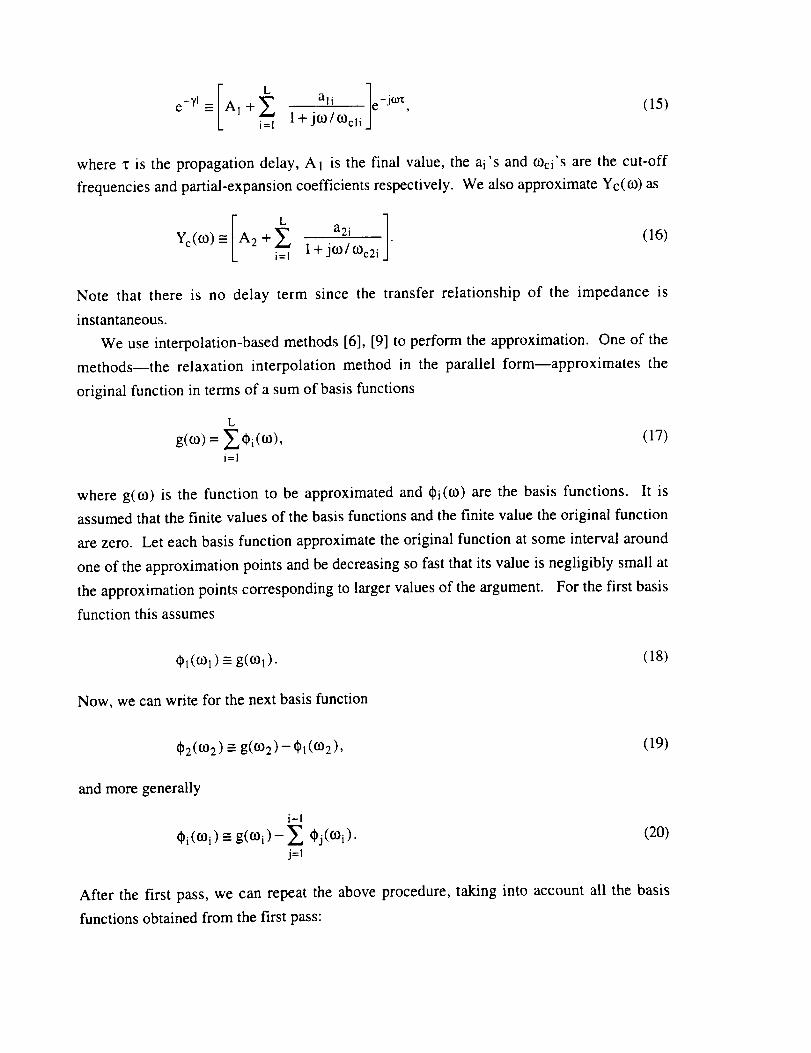
t ' ]e-YI -- AI + Z ali e-Jttrc'l+jco/i=l cocli
(15)
where "r is the propagation delay, A I is the final value, the ai's and coci'S are the cut-off
frequencies and partial-expansion coefficients respectively. We also approximate Yc(cO) as
I ' 1Yc(cO) = A2 + Z a2i "i=l I + JCO/COc2i
(16)
Note that there is no delay term since the transfer relationship of the impedance is
instantaneous.
We use interpolation-based methods [6], [9] to perform the approximation. One of the
methods--the relaxation interpolation method in the parallel form--approximates the
original function in terms of a sum of basis functions
L
g(cO) = EI_)i(cO), (17)
i=l
where g(cO) is the function to be approximated and Oi(cO) are the basis functions. It is
assumed that the finite values of the basis functions and the finite value the original function
are zero. Let each basis function approximate the original function at some interval around
one of the approximation points and be decreasing so fast that its value is negligibly small at
the approximation points corresponding to larger values of the argument. For the first basis
function this assumes
Ol (c°l) = g(cO] )"
Now, we can write for the next basis function
(18)
_2(cO2) = g(cO2)- Ol(CO2), (19)
and more generally
i-I
_)i(cOi) --- g(cOi)-- E (Dj(cOi)"
j=l
(20)
After the first pass, we can repeat the above procedure, taking into account all the basis
functions obtained from the first pass:

L
(_i(03i) _ g(03i)- ,','_ (_j((Oi)'
j=lj#i
(21)
After this second pass, the difference between the original and approximating functions
will be reduced, because an influence of all the terms was accounted more accurately during
the calculation of the approximation parameters. The procedure may be repeated to achieve
a desired accuracy.
The following summarizes the steps involved in applying the real-part parallel relaxation
interpolation method to Yc(03). In this case, Yc(o) is being approximated as
I _ l+jo/03ciaiYc(03)= A +i=t
Let g be the real part of Yc, then
aig(03)= A + 032i=l 1+ / 0,)ci
1. Choose approximation interval: 2L+I frequency points.
2. Sample original function at the frequencies 03k
3. Reverse the order of the samples.
4. Initialize ai = 0, 03i = 1, i = 1, 2 ..... L.
REPEAT until a desired accuracy tolerance is attained
(22)
(23)
7= 03m_x ,k=0, 1 ..... 2L.
A = g(03max ) - Eaj
2 2'j=l 1 + 03max/03cj
(24)
FOR
i runs as 1, 2 ...... L
032 = 0i(032i){1)_i- 0i(032i-1)¢D2i-1
0i (032i-1) -- 0i(032i) (25)
a i -'0i(f_2i) 1+-77Y-/,O_ci )
(26)
where
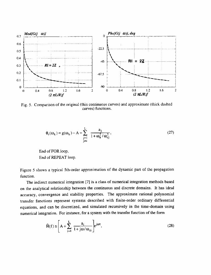
Mod{G(j to)}0.7 _ 1 r
0.6 ........................................_......................................................
0.5 ........................................:...................................._...................
::: .........:................: :... :
0.1
0 0.4 0.8 1.2 1.6 2
(2 _L/R)f
Phs{G(j to)}, deg0 I
-22.5
-45 RI = 2_
-67.5
-900 0.4 0.8 1.2 1.6
(2 aL/R )f
Fig. 5. Comparison of the original (thin continuous curves) and approximate (thick dashedcurves) functions.
L ajOi((t)k) = g(_k ) -- A - Z
j=l I+(02/0")2'j#i
(27)
End of FOR loop,
End of REPEAT loop.
Figure 5 shows a typical 5th-order approximation of the dynamic part of the propagation
function.
The indirect numerical integration [7] is a class of numerical integration methods based
on the analytical relationship between the continuous and discrete domains. It has ideal
accuracy, convergence and stability properties. The approximate rational polynomial
transfer functions represent systems described with finite-order ordinary differential
equations, and can be discretized, and simulated recursively in the time-domain using
numerical integration. For instance, for a system with the transfer function of the form
a,]I7-I(f) = A+ 1 + j60/ eJ°_'i=1 (Dci(28)

the step-response invariant indirect numerical integration formulas in the parallel canonic
form are given by
L
y[nT] = Ax[(n - k)T] + y__,Ypi [nT],i=l
(29)
where
Ypi [nT] = a i (1 - e-t°_'T)x[(n - k - I)T] + e-t%Typi [(n - 1)T], (30)
x is the excitation, y is the system response, T is the time step and k is the discrete-time
delay.
After the characteristic admittances and propagation functions have been discretized, the
frequency-domain element characteristic (13) turns into the discrete-time element
characteristic--the companion model--which is used by a circuit simulator to represent
distributed lines, and is recursively updated at each time iteration via numerical integration
formulas.
Figure 6 presents the comparison of the simulation results obtained with the optimal
method and segmentation method (separating delays and losses). The network and line
parameters are: Rl=50 _, R2=l kf2, C=39 pF/m, L=539 nil/m, R=125 f2/m, G=0, 1=0.675
m. The following voltage pulse with linear rise and fall was taken for the excitation: El=4
V (start time ts=5 ns, rise time tr=l ns, pulse width tw=20 ns, fall time tf=l ns), E2=0. The
time-step T=0.5 ns. As can be observed, the results are in excellent agreement.
IV. Conclusions
Two methods of distributed line simulation were discussed--the scattering-parameter
method and the optimal method. The scattering-parameter method permits a straightforward
implementation of voltage wave solutions but is computationally expensive as a result of
convolution calculations. The optimal method results in the maximum efficiency, accuracy
and practical applicability with respect to the transient analysis of digital circuits. The
optimal line model can be directly used in a circuit simulator, and lines can be characterized
with frequency or time-domain data samples. The efficiency of the optimal method allows
for an accurate simulation of real circuits, containing thousands of multiconductor
nonuniform frequency-depend lines and nonlinear active devices, with virtually no increase
in the simulation time compared to the replacement of interconnects with lumped resistors.
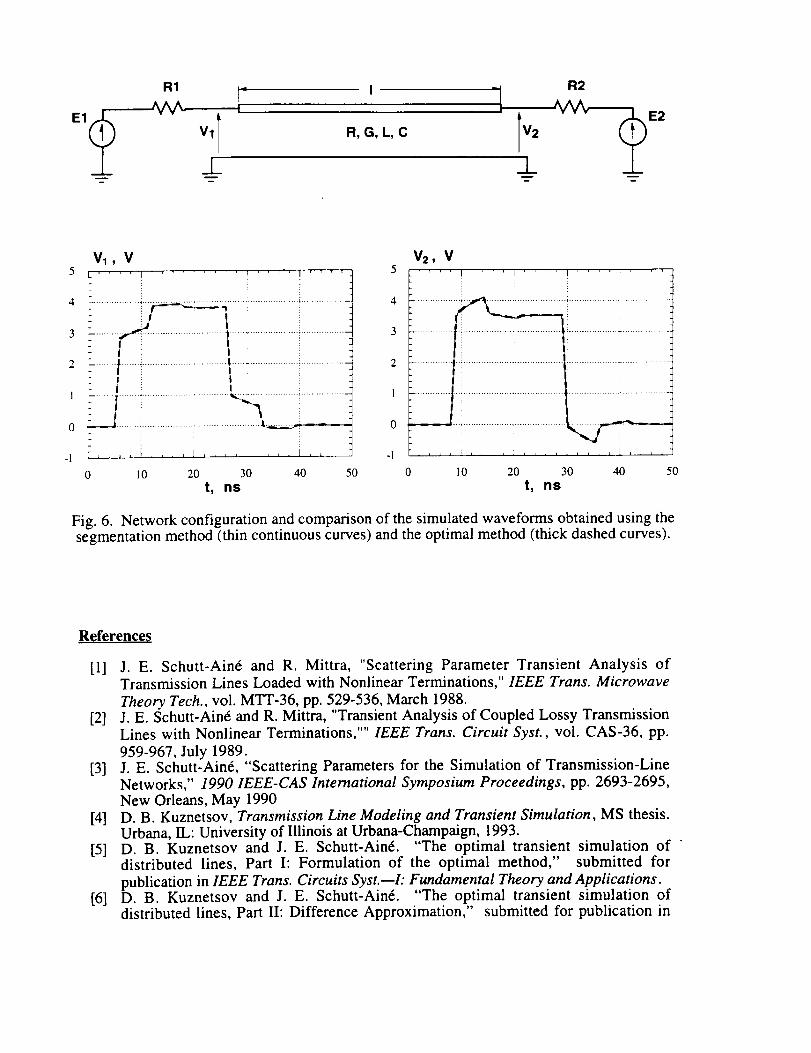
R1
EI_ V1_L_
I
R, G, L, C "L R% E2Tv2/
Vl, V5 L ........ I .... 1 ........
_
-.........F ...........................i..........................i..................- ............... i................................. ! ............................................
'! ti ti,- .......I......!..................._............,_ .................;..................
-I s .... i .... I .... i .... L , ,
0 10 20 30 40 50
t, ns
2
1
0
-1
V2, V5
0 I0 20 30 40 50
t, ns
Fig. 6. Network configuration and comparison of the simulated waveforms obtained using thesegmentation method (thin continuous curves) and the optimal method (thick dashed curves).
References
[I] J. E. Schutt-Ain6 and R. Mittra, "Scattering Parameter Transient Analysis ofTransmission Lines Loaded with Nonlinear Terminations," IEEE Trans. Microwave
Theory Tech., vol. MTT-36, pp. 529-536, March 1988.[2] J.E. Schutt-Ain6 and R. Mittra, "Transient Analysis of Coupled Lossy Transmission
Lines with Nonlinear Terminations,"" IEEE Trans. Circuit Syst., vol. CAS-36, pp.
959-967, July 1989.[3] J. E. Schutt-Ain6, "Scattering Parameters for the Simulation of Transmission-Line
Networks," 1990 IEEE-CAS International Symposium Proceedings, pp. 2693-2695,
New Orleans, May 1990[4] D.B. Kuznetsov, Transmission Line Modeling and Transient Simulation, MS thesis.
Urbana, IL: University of Illinois at Urbana-Champaign, 1993.[5] D. B. Kuznetsov and J. E. Schutt-Ain6. "The optimal transient simulation of "
distributed lines, Part I: Formulation of the optimal method," submitted for
publication in IEEE Trans. Circuits Syst.--l: Fundamental Theory and Applications.[6] D. B. Kuznetsov and J. E. Schutt-Ain6. "The optimal transient simulation of
distributed lines, Part II: Difference Approximation," submitted for publication in

IEEE Trans. Circuits Syst.--l." Fundamental Theory and Applications.[7] D.B. Kuznetsov and J. E. Schutt-Ain6. "Indirect numerical integration," submitted
for publication in IEEE Trans. Circuits Syst.--l: Fundamental Theory and
Applications.[8] D. B. Kuznetsov and J. E. Schutt-Ain6. "The optimal transient simulation of
nonuniform distributed lines," submitted for publication in IEEE Trans. Circuits
Syst.--l: Fundamental Theory and Applications.[9] D. B. Kuznetsov and J. E. Schutt-Ain6. "Modified direct rational interpolation
method for the frequency-domain difference approximation," in preparation.

Difference Model Approach for the Transient Simulation of Transmission Lines
Dmitri Kuznctsov and Josd E. Schutt-Ain6
Elec_'omagnetic Communication Laboratory
Department of Electrical and Computer EngineeringUniversity of Illinois
1406 West Green SweetUrbana, Illinois 61801-2991 USA
Abstract--An optimal technique (in terms of computationalefficiency, accuracy, and practical applicability) for the tran-sient simulation of distributed multiconductor RLGC lines wasdeveloped by applying the indirect numerical Integrationmethod (the most effident and accurate transient simulationmethod) to the device model for a distributed line (the most ef-ficient and practically applicable model). The technique can bedirectly used in a circuit simulator. The computationalcomplexity is linearly proportional to the number of time-steps.Nonuniform tines, lines with frequency-dependent parameters,and real Ilnes, characterized with a few samples of time- or fre-quency-domain measurements or electromagnetic simulations,can be accurately and efficiently simulated.
I. INTRODUCTION
The transientsimulationof distn'butedlineshas gained
specialimportancewith thedevelopment of high-speeddigi-
talelectronics.Previouslydeveloped techniquesarequitedi-
verse,but not alwayscomputationallyefficientand applicable
torealcircuitsin which distributedlinesare surrounded by
thousandsof activedevices. In [I]an attemptwas made to
develop a techniquethatwould be optimalincomputational
efficiency,accuracy,and applicabilitytorealproblems. The
resultsobtainedin[I]aresummarized inthispaper.
II. SYSTEM MODEL FOR A DISTRIBUTED LINE
The system-diagram representation of a single line is
shown in Fig. I. Wv/and Wvb represent the forward andbackward voltage propagation functions, respectively; TI, 1"2
and 1-1, 1"2 are the near- and far-end transmission and reflec-
tion coefficients, respectively.The system-diagram representation of a multiconductor
line is given in Fig. 2. WVm f and Wvmb arc the diagonal
forward and backward modal voltage propagation functionmatrices; Tt, T2 and 1"1, rl represent the near- and far-end
transmission and reflection coefficient matrices: and Mvt,
Mvb are the forward and backward modal voltage transfor-
E'/'_Termination _,s .... ,,'-_,Termination_'_ 2
he,workI K' network2
Fig. I. System model for• single line.
0-7803-1254-6/93503.00 © 1993 IEEE
½
o-El2 .-
: '_
N+ I - conductor fine
Fig. 2. Systemmodel for• multicondscmrline.
marion matrices.
The models reproduce the general relationship between thephysical processes of wave propagation, reflection, andcoupling in a distributed system and can represent arbitrarydistributed systems such as uniform and nonuniform trans-
mission lines, waveguides, and plane-wave propagation. Fordistributed RLGC lines, the mathematical justification of themodels was obtained [1]. The models can be used for systemanalysis of distributed networks. They also allow one to ob-tain the solution for a distributed system without complexmathematical derivations.
From Figs. 1 and 2, it can be observed that a distributed
line along with the terminations forms a feedback system.This explains why a global-parameter characterization (suchas Z-, Y-, H-, or S-parameter characterization) results in com-
plex,non-monotonous functions for the parameters. A directcharacterization in terms of open-loop transfer functions (thepropagation functions) leads to simpler transfer functions andtransient characteristics and should be used for the transientsimulation.
HI. DEVICE MODEL FOR A DISTRIBUTED LINE
Distributed line models can be divided into circuit and
non-circuit models. Non-circuit models cannot be directly
inserted into a circuit simulator, and, consequently, can not beapplied with efficiency for the transient analysis of real cir-cuits. The system models described in the preceding sectionmay serve as an example of non-circuit models.
Circuit models can be directly placed into a circuit simula-tor, and, therefore, are of prime practical interest. They relate
1547
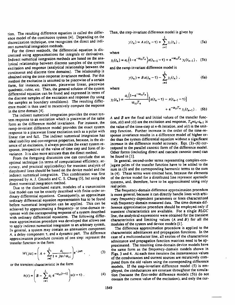
tion. Theresultingdifferenceequationis called the differ-ence model of the continuous system [4]. Depending on the
discretization technique, one recognizes the direct and indi-rect numerical integration methods.
For the direct methods, the differential equation is dis-
cretized using approximations for integrals or derivatives.Indirect numerical integration methods are based on the ana-
[ydca| relationship between discrete samples of the systemexcitation and response (analytical relationship between thecontinuous and discrete time domains). The relationship is
obtained using the time-response invariance method. For thismethod the excitation is assumed to be piecewise of a certainform, for instance, staircase, piecewise linear, piecewise
quadratic, cubic, etc. Then, the general solution of the systemdifferential equation can be found and expressed in terms of
the discrete samples of the excitation and response (by usingthe samples as boundary conditions). The resulting differ-ence model is then used to recursively compute the response
in the time domain [4].The indirect numerical integration provides the exact sys-
tem response to an excitation which is piccewise of the sameform as the difference model invariance. For instance, the
ramp-invariant difference model provides the exact systemresponse to a piecewise linear excitation such as a pulse withlinear rise and fall. The indirect numerical integration has
ideal stability and convergence properties, because, in the ab-sence of an excitation, it always provides the exact system re-
sponse, irrespective of the value of time step and form of in-variance. It is also more accurate than the direct method.
From the foregoing discussion one can conclude that an
optimal technique (in terms of computational efficiency, ac-curacy, and practical applicability) for transient analysis ofdistributed lines should be based on the device model and the
indirect numerical integration. This combination was first
proposed by A. J. Gruodis and C. S. Chang [5], but using thedirect numerical integration method.
Due to the distributed nature, modules of a transmissionline model can not be exactly described with finite-order or-
dinary differential equations. Consequently, an approximateordinary differential equation representation has to be foundbefore numerical integration can be applied. This can beachieved by approximating a frequency- or time-domain re-sponse with the corresponding response of a system describedwith ordinary differential equations. The following differ-ence approximation procedure was developed that allows oneto apply indirect numerical integration to an arbitrary system.In general, a system may contain an attenuation componentA, a delay component x, and a dynamic pan. The differenceapproximation procedure consists of one step: represent thetransfer function in the form
W(j¢o) = A + e , (3)/=II+ jcoI tOci
or the transient characteristic in the form
I 1h(t) = B- _a i e -t°ci(t-x) u(t-z) . (4)i=1
Then, the step-invariant difference model is given by
L
Y(tn) = Ax(t n -'¢) + Eyi(tn) , (5a)i--I
where
Yi (tn) = ai (1 - • -_ciTn )X(tn_ 1 - "¢)+ e -''aTn Yi (tn-I) , (5b)
and the ramp-invariant difference model is
L
y(tn) --- Bx(t n -z) - _._),i(tn) , (6a)i---I
where
"i (l- r" Irat.)= J[x(t.-,0- xft._l-x)]
cociJ,
+ e-C°cir" Yi(tn-1) • (6b)
A and B are the final and initial values of the transfer func-
tion, x(t) and )_t) are the excitation and response, Tn=tn-tn.! isthe value of the time-step at n-th iteration, and u(t) is the unit-
step function. Further increase in the order of the time-re-sponse invariance results in a difference model of higher or-dei" than the system differential equation without a significantincrease in the difference model accuracy. Eqs. (3)-(6) cor-re.Cpond to the parallel canonic form of the difference model.
Other forms (including direct and cascade canonic ones) canbe found in [11.
In general, second-order terms representing complex-con-jugate poles of the transfer function have to be added to thesum in (3) and the corresponding harmonic terms to the sumin (4). These terms were omitted here, because the elementsof the device model for a distributed line represent aperiodicsystems, and, therefore, have to be approximated using onlyreal poles.
The frequency-domain difference approximation procedureis more general, because it can directly handle lines with arbi-trary frequency-dependent parameters or lines characterized
with frequency-domain measured data. The time-domain dif-ference approximation procedure should be employed only iftransient characteristics are available. For a single RLGCline, the analytical expressions were obtained for the transientcharacteristics and limiting values (A and B) for all themodules of the system and device models [1 ].
The difference approximation procedure is applied to thecharacteristic admittances and propagation functions. In thecase of a multiconductor line, all entries of the characteristic
admittance and propagation function matrices need to be ap-proximated. The resulting time-domain device models havethe same form as the frequency-domain models shown inFigs. 3 and 4. At each time iteration the instantaneous valuesof the conductances and current sources are re.cursively com-puted from the old values using the corresponding differencemodels. If the step-invariant difference model (5) is em-ployed, the conductances are constant throughout the simula-tion (because the first-order difference models (5b) do notcontain the current value of the excitation), and only the cur-
1549

.,¢tricc/ionwdervolu-harear incond-
4,hichmdOfl
eUmi-
ndentreinS.
lielec-
ied by
videlyiielec-
aation
_neral,
wever,relate
body,nly ons of a
ditions
and is
quency
lomain
_s beenmre of
tzation of
:net/¢ and
!
TRANSACTIONS ON _AS AND PROPAGATION, VOL. 43, NO 7, JULY 1995 _ i PROPAGAT/ON. VOL. 43, NO 7, .rULY 1995
ementation of Surface
.ary Conditions for the
Time-Domain Method il i I
_EE and Jose E. Schutt-Aine, Member, IEEE
_mee the SIBC, it is represented by a convolution integral in the
main time domain. Tesche [6] has formulated a time-domain integral iJ.
equation based on this convolution integral and pointed out
that the direct computation of this convolution integral is
impractical due to the large computation time and storage
requirements. On the other hand, Maloney and Smith [7] have
applied the SIBC to the finite-difference time-domain method.
To overcome the computational difficulties associated with the
convolution integral, they use an approximate recursive for-
mula. Their implementation, however, requires the exponential
approximation to be performed prior to the FDTD simulation.
Beggs et al. [8] have eliminated this preprocessing time by
performing the exponential approximation based on the highconductivity surface impedance approximation. It should be
noted that when the SIBC is applied to the finite-difference
time-domain (FDTD) method, in addition to the reduction of
discretization space, further computational saving is achieveddue to the larger discretization step compared to that for the
nonreduced original problem. A detailed discussion of this
computational saving is given in [7] and [8].
In this paper, the implementation of the SIBC in the FDTDmethod is considered for a lossy dielectric half-space and
a thin lossy dielectric medium. For a lossy dielectric half-
space, the normalized impedance function for a lossy medium
is approximated in the frequency domain using a series offirst-order rational functions. Since the normalized impedance
function used in this paper is independent of medium proper-
ties, the rational approximation has to be performed only once.
The results of this approximation are tabulated for rational
functiom of various orders. Then, using the approximate
normalized impedance function and assuming the waves to be
piecewise linear in time, a closed-form expression is derivedto evaluate the time-domain convolution integral recursively.
Thus, the presented formulation is numerically more efficient
than that in [7] because the preprocessing time for the expo-
nential approximation is eliminated and more accurate thanthat in [8] since the high conductivity approximation is not
utilized.
Although several methods have been proposed to model a
thin lossless dielectric shell for the FDTD method [9]-[12],
lime work has been performed for a perfect electric conductor-
(PEC-)backed P lossy dielectric shell in spite of its frequent
occurrence in practical problems. A full time-domain imple-mentation of the SIBC, which accounts for the frequency
_26X/95504.00O 1995 IEEE
i J
t
4 6
Frequency (GHz)
the FDTD simulauon.
ABC boundary12-order Mur}
,'_. p_. B Obs. pt. C
0. 32.5) (32.5.32.5)
,o_ ,0 ffi 20 S/m
8 10
_40. 401
:ree Space
x (cm)
)-dtmens,onal TM FDTD example.
ler tsee Fig. 6). The simulation isormal FDTD and the SIBC FDTD_ers
_m
it-o.646x io-I°)/o.1874x lO-_X)2
alation results of the normal FDTD
veil at the observation point B. andfor the points A and C. The sameusing the SIBC FDTD with five
.' steps than for the previous ones.
imensional plot of the simulation_rmal FDTD simulation, whereas
, from the SIBC FDTD with the
_gh the same excitation is used for
excitation 4 and difference in the
w.e excitation is added to the FDTD field
,erea_. in the hard excitation, the source
at the excitaUon potht.

6645 [FEE TRANSACTIONS ON ANTENNAS AND PROPAGATION. VOL. 43. NO, 7. JULY 1995
REFERENCES
[ 1] M.A. Leontovich. "On the approximate boundalw, condieions for elecll'o-
magneuc fields on the surface of well conducung bodies," in lnvesUga.
uons of Propagation of Radto Waves, B. A. Vvedensky. Ed. Moscow:Academy of Sciences USSR. 1948. pp. 5-20.
[2] T. B A. Senior. "Impedance boundary conditions for imperfec0y
conducting surfaces,"Appl.Sci.Res.,vol.8.S¢c. B. pp. 41g--,436.1960.
[3] _, "'Approximate boundary condiuons," IEEE Trans. Antennas
Propagat., vol. AP-29, pp. 826-829° Sep. 1981.
[4] K.M. Mim2er, "An integral equauon approach to scattenng from a bodyof fimte conductivity," Radio Sci., vol. 2, pp. 1159-1470, Dec. 1967.
[51 _, "Effecpve boundary condiuons for reflccuon and transnussion
by an absorbing shell of atbiu'a,,,'y shape," IEF__ Trans. Antennns Prop.agat.,vol. AP-16. pp. 706-712. Nov. 1968,
[6] F. M. Tesche, "On the inclusionof loss in time-donuun solutions
of elecn'omagneuc interacuon problems," IEEE Trans. Electromagn.
Compat.. vol.32. pp. I--4.Feb. 1990.
[7] J.G. Maloney and G. S. Snmh, "The use of surfaceimpedance concepts
in the finite-difference time-domain method," IEEE Trans. Antennas
Propagat., vol. 40, pp. 38-48, Jan. 1992.[8] J. H. Beggs, R. J. Luebbers. K. S. Yee. and K. S. Kunz. "'Finite-
difference nine-domain tmplementauon of surface impedance boundary
conditions," IEEE Trans. Antennas Propagat., vol. 40, pp. 49-56. Jan.1992.
[9] J. G. Maloney and G. S. Snuth. "The efficient modeling of thin materialshells in the finite-difference time-don_un (F'DTD) method." IEEE
Trans. Antennas Propagat.. vol. 40. pp. 323-330. Mar. 1992.[ l 0] R.J. Luebbers and K. Kunz. "F-'DTD modeling of thin Bmpedance shells."
IEEE Trans. Antennas Propagat., vol. 40. pp. 349-351. Max. 1992.
[ l I ] L.-K. Wu and L.-T. Ham. "'Implementauon and application of resistive
sheet boundary condition in the finite-difference time--domain method,"IEEE Trans. Antennas Propagat.. vol. 40, pp. 628--633. June 1992.
[12] P. A. T_kas and K. R. Demarest. "Modehng of thin dielecmc scruc-
lures using the finite-difference time-domain technique.'" IEEE Trans.
Antennos Propagat.. vol. 39. pp. 1338--1344. Sept. 1991.[13] S. Wolfram. Mathemauca. Reading. MA: Addison-Wesley, 1991.
Kyung Suk Oh _SM'911 was born m Pusan. SouthKorea. in 1965. He received the B.S. and M.S.
degrees inelecmcaJ engmeenng from the Umven)ty
of Illinois.Champaugn. m 1990 and 1992, respec-
tively,
Since 1990. he has been involved in research
work on modeling and slmulauon of high speed
d/gital circuits in the elecu'omagnetic commumca-
uon laboratory at the University of Illinois, where
he is pursuing the Ph.D. degree.
Jme F. Schutt-Aine fs'g7-M'88) received the B.S.
degree from Massachusetts Institute of Technology,
Cambridge. MA. and the M.S, and Ph.D. degreesfrom the University of Illinois. Urbana. m 1984 and
1988. respectively.
Following graduation from MIT. he spent two
years with Hewleu-Packard Microwave TechnologyCenter in Santa Rosa. CA. where he worked as a De-
vice Application Engmeer. While pursuing graduatestudies at the University of Illinois, he held summer
positions at GTE Network Systems in Northlake.
IL. He is presently serving as an Assistant Professor in the Department ofElecmcal and Computer Engineenng at the University of Illinois. His curt'era
research interests are microwave theory and measurements, electromagneucs.high-speed digital circuits, solid-state electromcs, circuit design, and electromc
packagmg.
]

Computation of Excess Capacitances of Various StripDiscontinuities Using Closed-Form Green's Functions
Kyung S. Oh, Jose E. Schutt-Aine, and Raj Mittra
Abstract--An efficient quasi-static method to compute excess (equivalent)capacitances of various strip discontinuities in a multilayered dielectric medium ispresented. The excess charge distribution on the surface of a conductor isobtained by solving an integral equation in conjunction with closed-form Green'sfunctions. A complete list of expressions of the closed-form Green's functionsfor a point charge, a line charge, and a semi-infinite line charge is presented. Anopen end, a bend, a step junction and a T junction are considered as numericalexamples.
I. INTRODUCTION
uasi-static analysis is often performed to characterize strip discontinuities when thedimensions of the discontinuities are much smaller than the wavelength. Under the quasi-
static analysis, the dominant effect of strip discontinuities is fringing fields due to the physical
irregularities of discontinuity geometries. The modeling of these fringing fields in terms of an
excess capacitance is discussed in this paper.
Numerous papers have been published to compute excess capacitances of various microstrip
discontinuities, and a summary of popular methods can be found in [1]. The most successful
approach is one based on the formulation of an integral equation in terms of the excess charge
distribution, which was first proposed by Silvester and Benedek [2] and has been applied to
analyze various microstrip discontinuities [2]-[5]. The Green's function for a layered medium is
employed in this approach. For N dielectric layers, the expression for this Green's function would
consist of an N-1 nested infinite series [6]; hence, in practice, this form of the Green's function
may not be applied to a multilayered medium. Recently, Sarkar et al. [7] solved discontinuity
problems for a multilayered medium using the free-space Green's function, but additional
unknown charges (over unknown charges on the surface of a conductor) had to be placed on the
dielectric interfaces and the top ground plane to model the polarization charge and the free charge.
Although such inclusion of unknowns may be tolerable for 2-D problems, it is computationally too
burdensome for 3-D problems.
In this paper, the closed-form Green's function discussed in [8] is employed to formulate an
integral equation in terms of the excess charge distribution. A complete list of expressions of the
closed-form Green's functions for a point charge, a line charge, and a semi-infinite line charge

with or without a top ground plane is presented in this paper. The presented method requires
neither additional unknowns to model dielectric interfaces and the top ground plane nor evaluations
of any infinite series except for cases where the top ground plane is present. When the top ground
plane is present, using the closed-form Green's function is still numerically advantageous since the
nested infinite series in the expression of the usual Green's function becomes a simple infinite
series without nesting.
II. CLOSED-FORM GREEN'S FUNCTIONS
Closed-form expressions of the electrostatic Green's functions for a point charge, a line
charge, and a semi-infinite line charge are derived in this section based on the approach used in [8].
Consider N dielectric layers which are backed by a ground plane as depicted in Fig. 1. The Nth
layer is either a half-space or terminated by an optional top ground plane. All dielectric layers and
ground planes are assumed to be planar and infinite in the xz-plane. The electrostatic Green's
function in the spectral domain is described by the following closed-form formula [8]:
_(T,y[ro) = 1 (K?(T,m,n)e?,(y+yo_2dn) + Kf(_t,m,n)e?,(y_yo+2(dm_,_dn))2Em_"
+ K_ (_,m,n)e_'(-Y+ Yo) Y >-Yo Cla)+
G(?', ylro) = 21i( K? (r,m,n)e _'(y+y°-2am),,.+ K_ (_,,m,n)e _(y-yo)
+ Kf (_t, m,n )e?_(-Y+ yo +2( dn-l -dm )) K4()',m,n) e_'(-y-y°+2d"-l)) Y< Yo (lb)+
where ¢_ is the spectral-domain Green's function, and r and ro are the observation and source
points located in the nth and mth layers, respectively. The superscripts + and - are used to denote
the cases for y > Yo and y < Yo. The expressions for the four coefficient functions K/t: can be
found in [8]. A closed-form expression of the Green's function in the space domain is obtained by
approximating these four coefficient functions K/:t using exponential functions. It is important to
mention that although K + is dependent on m and n, it is not a function of y and Yo; hence, the
approximation can be performed without any prior knowledge of the junction geometry. The
following two subsections detail the derivation of the closed-form Green's functions due to a point
charge, a line charge, and a semi-infinite line charge with or without the top ground plane.
A. Closed-Form Green's Functions for Geometries Without the Top Ground Plane

When there is no top ground plane, the four coefficient functionsK + in (la) or (lb) are
nonoscillatory and smooth functions of 7; hence, each coefficient function can be sufficiently
approximated with real-valued exponential functions as follows [8]:
+Nm,n,i
• ±,)
K_(m,n,7)= _ C +'; e a".",A' i=1,2,3,4 (2)- rn,n,i-j=l
where N+n,i denotes the number of exponential functions used in the approximation of K +,
which typically ranges from 5 to 10. The exponential functions used in the spectral-domain
approximation can be physically interpreted as weighted images in the space domain [8].
Compared to the exact Green's function in the space domain, which consists of an infinite number
of images, the expression for the closed-form Green's function consists of only a finite number of
weighted images.
Once the exponential approximation is performed in the spectral domain, the closed-form
Green's functions for 2-D and 3-D can be obtained in the space domain by using the inverse
Fourier transformation formulas (14a) and (14b) in [8], and the resulting expressions are given by
4
G2D(PlPo)= -11 fi 2D'++'(pIpo)2ZCEmi=1
(3a)
4
G3D(rlro)= I i_ 14_ m fi3D'+ (rl ro)(3b)
For i=1 and y > Yo, the expressions of f/2D,+ and ft.3D'+ are given by
+gm,n.I
fl2D'+(PIPo ) E +'j (_ +,j )2) (4a)= C_n,n,1 .ln (X-Xo) 2 +(Y+Yo -2dn +am,n,l
j=l
+
Nm,n,l Cm+,J,n,1
+,j )2+ (Y + Yo - 2dn + am,n,l + (Z- Zo) 2
(4b)
Similar expressions can be obtained for f/2D,+ and f/3D,+ for other values of i.
To derive the Green's function for a semi-infinite uniform line charge, the auxiliary Green's
function for a line charge with polarity reversal is employed [2]. Consider a uniform line charge,

which starts from z = _ and is infinitely extended in the positive z-direction; then the Green's
function for a semi-infinite line charge G semi can be expressed as
Gsemi(rlro,_) = 2[G2D(plpo)+ GP(rlro,_)] (5)
where G semi is the Green's function for a line charge with an abrupt polarity reversed from minus
to plus at z = 4. The expression for G p is obtained by integrating the potential due to a point
charge [2]:
4 p,+GP (rlro, 4) = - _ 63 O (r[r ° ) + _63 O (rlr ° ) = _ E fi -(rlro, 4)
--o, a 4_Em i=1
(6)
Again, for i= 1 and y > Yo, fi p'+- is given by
+
Nm.n,l
f P'+(rlro' ) = Ej=l
__<= >= i/j+.j -Xo) 2+(y+yo-2dn+am,n,I +(Z-_) 2 +(z-_) (7)Cm,n," lnl [ +,j -
(x Xo)2 +(y+ yo 2dn +arn,n,l +(z 4) 2 (z
B. Closed-Form Green's Functions for Geometries with the Top Ground Plane
When the top ground plane is present, all of the four coefficient functions K/:t are still
nonoscillatory but contain a pole at )' = 0; as a consequence, K + can no longer be accurately
approximated with exponential functions [8]. To overcome this difficulty, let us rewrite G in the
following manner:
d( r, ylro) = Rm,. h (r, ylro) + (r, ylro) (8)
where (_h is the spectral-domain Green's function for a homogeneous medium, i.e., all dielectric
layers are replaced by the source layer. Rm, n is a const.ant which is determined such that (_h
contains a pole at 7' = 0 and (_' is a well-behaved function without any poles. Rm, n can be
obtained either numerically or analytically by taking limits of (_ and (_h as 7' _ 0. Now the
technique used in the previous section can be applied to obtain the closed-form expression for G'
in the space domain, and the space-domain expressions of (_ are obtained once the corresponding
expressions of (_h are determined.
Expressions of t_ h in the space domain can be easily obtained using the image theory approach
and are given by
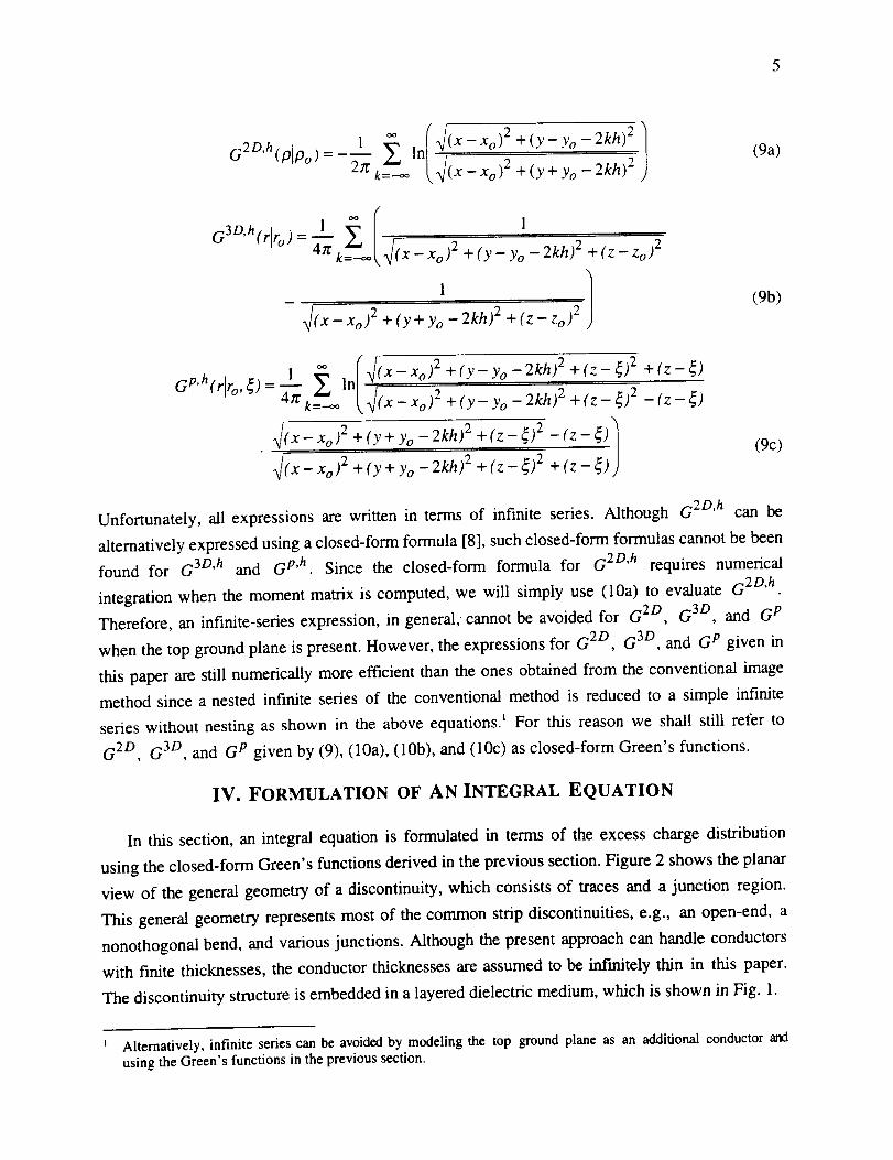
5
G2D, h(p]po) -1 "_ ln(_/(X-Xo)2+(._._.yy-y..yo-2kh)2 I2_ _-__..._ (_(x Xo)2 +(y+ yo 2kh)"---_
(9a)
_/(x - Xo) 2 +
- 2kh) 2 + (z - Zo)2
I(Y + Yo - 2kh )2 + ( z - Zo )2
(9b)
GP, h(rlro,_) =.._L _ ln(_/(x
4zr k=--oo _j(x
• _/(X-Xo) 2 +(y+
_/(X - Xo) 2 + (y +
- x°)2 + (Y - YO - 2kh)2 + (z - _)2 + (z - _)
Xo)2+(Y Yo 2kh)2+(z-_)2-(z _)
Yo - 2kh) 2 + (z - 4) 2 - (z - 4) I
Yo 2kh) 2 +(z 4) 2 +(z 4) J (9c)
Unfortunately, all expressions are written in terms of infinite series. Although G 2D'h can be
alternatively expressed using a closed-form formula [8], such closed-form formulas cannot be been
found for G 3D'h and G p'h . Since the closed-form formula for G 2D'h requires numerical
integration when the moment matrix is computed, we will simply use (10a) to evaluate G 2D'h .
Therefore, an infinite-series expression, in general, cannot be avoided for G 2D, G 3D, and G p
when the top ground plane is present. However, the expressions for G 2D, G 3D, and G p given in
this paper are still numerically more efficient than the ones obtained from the conventional image
method since a nested infinite series of the conventional method is reduced to a simple infinite
series without nesting as shown in the above equations, t For this reason we shall still refer to
G 2D, G 3D, and G p given by (9), (10a), (10b), and (10c) as closed-form Green's functions.
IV. FORMULATION OF AN INTEGRAL EQUATION
In this section, an integral equation is formulated in terms of the excess charge distribution
using the closed-form Green's functions derived in the previous section. Figure 2 shows the planar
view of the general geometry of a discontinuity, which consists of traces and a junction region.
This general geometry represents most of the common strip discontinuities, e.g., an open-end, a
nonothogonal bend, and various junctions. Although the present approach can handle conductors
with f'mite thicknesses, the conductor thicknesses are assumed to be inf'mitely thin in this paper.
The discontinuity structure is embedded in a layered dielectric medium, which is shown in Fig. 1.
Alternatively, infinite series can be avoided by modeling the top ground plane as an additional conductor andusing the Green's functions in the previous section.

The integral equation relating the electrostatic potential 0 and the charge density q on the
surface of a conductor is given by
¢(r) = S G3D(rlr' )q(r' )dr' =(G3D,q) (10)1"2
where/'2 are the surfaces of a conductor: traces and a junction region. To simplify the notation the
integration is symbolically written as (.,-). Now let us rewrite the charge density q in the following
manner:
Then, (10) becomes
qj (r),
q(r)=[q_.(r),
if r is on the junction region
if r is on the ith trace(11)
N I
_(r)= (G3D,q) = (G3D,qj )+ E (G3D'q_') (12)i=l
Decomposing the charge densities q_- into the uniform charge density q_nif,i and the excess charge
exces$.idensity qT for each trace:
q_.(r) = q_.nif 'i (r) + excess,i, ,qT tr) (13)
.unif,i is obtained by solving a 2-D problem, in which it isHere, the uniform charge density ,.ST
assumed that only the ith trace is present in the medium and that the ith trace is infinitely long in
both directions. A detailed discussion for solving 2-D problems is given in [8]. The uniform
charge density q_nif,i exists only on the ith trace, which is a semi-infinite line; hence, G semi
should be used to compute the potential due to q_nif,i. Using (13), (12) can be written as follows:
N t
N, \ T ] \ //Gsemi'qunif'i\=/G3D'qj\+_",.-.3D excess.i\_(r) - E 2.,\ I-" ,qr /i=1 i=1
(14)
The integral equation (14) can now be solved by using the method of moments. The collocation
method is used in this paper. The closed-form formula for the integration involving G 3D is given
discussed in [8], whereas the integration involving G semi can be analytically integrated using the
following formula:

r'26221[ I / /f ln/_/a + + + a dl = 21DI tan -I all - tan-I . a12
J L4a2+b2+12_a ]bl_a2+b2+ll 2 Ibl_a2+b2+l
+2alnl12_+_a2+b2+122]+ ln(_a2+b2+122+a) ln(_a2+b2+ll2+_]it/l+_ ) 12 t_2+b2+122_a) -ll t_a2+b2+ll 2-(15)
Now once (15) is solved, the excess (equivalent) capacitance c e can be obtained by
ce = Qj + Q_xcess,i (16)
i=1
where Qj is the total charge on the junction region, and _excess,i_T is the total excess charge on the
ith trace. Throughout the formulation, we have assumed that the junction region exists between
traces. The formulation for cases without the junction region, such as an open end and step
junctions, can be easily obtained simply by removing terms corresponding to qj.
IV. NUMERICAL EXAMPLES
A computer program is written based on the technique discussed in the previous sections. The
program assumes that the shape of the junction region, (see Fig. 2), if it exists, is polygonal, and it
can handle an arbitrary number of dielectric layers as well as traces.
Excess capacitances for four common strip discontinuities, an open end, a step junction, a
bend, and a T junction, are computed using the program. The geometries of discontinuities with
their corresponding equivalent circuits are shown in Fig. 3. The following parameters are used: 1)
an open end: w = 0.5 mm, 2) a step junction: w1 = 0.1 mm and w2 = 0.2 nun, 3) a right-angle
bend: w t = w 2 =0.15 mm, and 4) a T junction: w t =w 2 = w 3 =0.15 mm. Three different types
of media are considered for each discontinuity with the following parameters (see Fig. 5): 1) an
open end: e1 = 4.2, t_2 = 2.5, Yl = 1.0 mm, Y2 = 1.5 mm, and Y3 = 2.0 ram, 2) a step junction:
el=6.0 , e2=4.2 , yl=0.1mm, Y2=0.2mm, and Y3=0.3mm, 3) a bend: e1=2.5,
e2=4.2 , yl=0.15mm, Y2=0.3mm, and Y3=0.5mm, 4)aT junction: e1=2.5 , e2=4.2 ,
Yl =0.15 mm, Y2 =0.3 mm, and Y3 =0.5 ram. All discontinuities are assumed to be embedded
at y = Yl. To place 3-D unknowns for the excess charge distribution, the length of each trace is
truncated at l = 8w. The total numbers of unknowns per each trace were 50 for a 2-D problem and
160 for a 3-D problem, whereas 100 unknowns were used for the junction region. The maximum
number of exponentials used to approximate each coefficient function K/:t was 5.

Thecomputedresultsareshownin TableI with thecomparisondatafor amicrostripcase(Fig.
4(a)).A goodagreementwasfoundoverallasshownin thetable.It is interestingto notethatforsomecasesthe valueof an excesscapacitanceturns out to be negative.Although a physical
capacitancemust be positive, an excess(equivalent)capacitanceis hypotheticaland can be
negative.
V. CONCLUSIONS AND FUTURE WORK
An efficient method to compute excess capacitances of strip discontinuities was discussed in
this paper. Complete expressions of closed-form Green's functions for a point charge, a line
charge, and a semi-infinite line charge have been derived. Unlike other approaches, only one
integral equation is employed in this paper to handle various strip discontinuities instead of
formulating an integral equation for each discontinuity type. The numerical results for a microstrip
case agreed well with other published results.
REFERENCES
[1] K.C. Gupta, R. Garg, and I. J. Bahl, Microstrip Lines and Slotlines. Norwood, MA:Artech House, 1979.
[2] P. Silvester and P. B. Benedek, "Equivalent capacitances of microstrip open circuits," IEEE
Trans. Microwave Theory Tech., vol. 20, pp. 511-516, Aug. 1972.
[3] P.B. Benedek and P. Silvester, "Equivalent capacitances for microstrip gaps and steps,"
IEEE Trans. Microwave Theory Tech., vol. 20, pp. 729-733, Nov. 1972.
[41 P. Silvester and P. B. Benedek, "Microstrip discontinuity capacitances for right-angle bends,
T junctions, and crossings," IEEE Trans. Microwave Theory Tech., vol. 21, pp. 341-346,May 1973.
[5] P. Silvester and P. B. Benedek, "Correction to 'Microstrip discontinuity capacitances for
right-angle bends, T junctions, and crossings'," IEEE Trans. Microwave Theory Tech.(letter), vol. 23, p. 456, May. 1975.
[6] C. Wei, R. F. Harrington, J. R. Mautz, and T. K. Sarkar, "Multiconductor transmission
lines in multilayered dielectric media," IEEE Trans. Microwave Theory Tech., vol. 32, pp.439-450, April 1984.
[71 T. K. Sarkar, Z. A. Maricevic, J. B. Zhang, and A. R. Djordjevic, "Evaluation of excess
inductance and capacitance of microstrip junctions," IEEE Trans. Microwave Theory
Tech., vol. 42, pp. 1095-1097, June 1994.
[81 K. S. Oh, D. B. Kuznetsov, and J. E. Schutt-Aine, "Capacitance computations in a
multilayered dielectric medium using closed-form spatial Green's functions," IEEE Trans.
Microwave Theory Tech., vol. 42, pp. 1443-1453, Aug. 1994.

9
OptionalTopGroundPlane
ENd, _1o
y=dNd
y=dNd-1
Bottom Ground Plane
y=d2
Y
y=dl ly=0
x
v
Fig. 1. Cross-sectional view of a multilayered dielectric medium.
S
Fig. 2. General geometry of a strip discontinuity.

10
l
(a) An open end
ce
I1 ,,,.._1_ 12
Wl _ w2
ll
(b) A step junction
v- I4
0ce
12
Ii,.._1v I
Ii,..._1v I
(c) A bend
J_,dl
c e
12
tl t3•J le
ll
v I
(3
12
0c e
(d) A T junction
Fig. 3. Discontinuities and their equivalent circuit representations.

11
_0 _ [J'O
--Yl
Bottom Ground Plane
(a) Medium 1
-- y=0 mm
_O _ _1, O
Bottom Ground Plane
(b) Medium 2
Y2
--Yl
y=0 mm
Top Ground Plane
Bottom Ground Plane
(c) Medium 3
-- Y3
-- Y2
--Yl
-- y=0 mm
Fig. 4. Three media considered for numerical examples.

12
OpenEnd
StepJunction
Bend
T Junction
TableI. Thenumericalresults(Unitsarein femtofarad).
Medium1
Computation Others
Medium2
Computation
Medium3
Computation
17.33
1.120
6.210
1.385
17.0 [1]
1.05 [ 1], 0.74 [71
6.75 [1], 5.8 [7]
1.9 [7]
23.52
1.352
7.006
-4.917
19.62
0.609
9.184
-0.818

Efficient Circuit Simulation of LossyCoupled Transmission Lines with
Frequency-Dependent ParametersDmitri Kuznetsov, C. Kumar and Jos6 E. Schutt-Ain6
D. B. Kuznetsov, J. E. Schutt-Aine
Dept. of ECE, M/C 702University of Illinois
1406 W. Green St.Urbana, IL 61801-2991, USA
Fax: (217)333-8986e-mail: vdm @decwa.ece.uiuc.edu
C. Kumar
Cadence Design Systems270 Billerica Rd.
Chelsmford,/vIA 01824Fax: (508)262-6600
e-mail: [email protected]
A b s t r a c t --This paper presents a method for the circuit simulation of uniform
multiconductor Iossy frequency-dependent lines characterized by sampled
frequency-domain responses. The implementation includes ac, dc and transient
analyses. The method combines element characteristics which do not require
introduction of current variables, open.loop characterization which results in the
simplest transfer functions, novel frequency-domain matrix rational
approximation method, novel matrix delay separation technique, and matrix
indirect numerical integration formulas. The method is reliable, accurate and as
efficient as the simple replacement of interconnects by lumped resistors.
I. INTRODUCTION
HE PROBLEM of the transmission line simulation gained special importance with thedevelopment of high-speed digital electronics. As transient times become faster, the
transmission line behavior of electronic interconnects starts to significantly affect transient
waveforms, and accurate modeling of on-board and even on-chip interconnects becomes an
essential part of the design process. The complexity of contemporary digital circuits calls for

2
accurate transmission line models efficient enough to perform the simultaneous circuit simulation
of thousands of lossy coupled frequency-dependent lines surrounded by thousands of nonlinear
active devices. Lines to be simulated may be characterized by measured or electromagneticly
simulated samples of their responses.
A substantial amount of study has been devoted to the transient simulation of transmission
lines in recent years [1]-[19]. This paper presents a method for circuit simulation of uniform
multiconductor lossy frequency-dependent transmission lines characterized by sampled frequency-
domain responses. The method is based on the approach described in [20]. The method supports
variable time stepping and has linear computational complexity. The method has been adopted in
several industrial and commercial circuit simulators, and, in numerous real-life simulation
exercises, proved to be reliable, accurate and as efficient as the simple replacement of interconnects
with lumped resistors.
The method employs element characteristics which do not require the introduction of
current variables. As a result, the method increases neither the number of nodes nor the number of
circuit variables, and the lines are incorporated into the circuit simulation without any increase in
the circuit solution time. Element characteristics for the ac and dc analyses are based on the Y
parameters.
For the transient analysis, the method uses open-loop transfer function characterization
(direct characterization in terms of the propagation functions and characteristic admittances), which
opens the feedback loop formed by the reflections from the terminations, and results in the simplest
characteristic responses. It is shown that the open-loop characterization is equivalent to the
generalized method characteristic.
The transient analysis is carried out by matrix indirect numerical integration. It has linear
computational complexity, and ideal convergence, accuracy and stability properties.
To apply numerical integration to the propagation functions and characteristic admittances
given as a set of frequency-domain samples, the method employs difference approximations. It
fits the samples with a rational polynomial function and expresses the numerical integration

3
formulasin terms of the approximation parameters. Because of the simplicity and aperiodicity of
the open-loop transfer functions, excellent approximation accuracy is attained with low-order real-
pole approximation and a few original samples.
The approximation is performed by novel matrix direct constrained method. The method
fits arbitrary number of arbitrary-spaced complex samples of a matrix transfer function with the
matrix rational polynomial functions with poles constrained to the left half of the complex plane to
insure stability. The method employs no iterative or relaxation techniques, only direct linear
solutions and a polynomial factoring, and is computationally efficient and free from convergence
problems.
Before the approximation, the delay is separated from the matrix propagation functions by a
novel matrix delay separation technique. The technique eliminates the problems associated with the
delay separation based on the diagonalization with the frequency-dependent modal transformation
matrices, which are nonminimum-phase functions of frequency with unstable time-domain
responses.
Throughout the paper, capital boldface, small boldface and normal italic symbols will be
used to denote matrices, vectors and scalars, respectively. Since only multiconductor lines will be
considered, the modifier "matrix" for the transfer functions will be omitted in the future for brevity.
II. FREQUENCY-DOMAIN LINE MODEL FOR TRANSIENT
ANALYSIS
The frequency-domain element characteristic (for the transient analysis) which does not require the
introduction of current variables and is suitable for the line modeling is given by
il (to) = Yt (to) vl (to) - Jl (to) ( 1)i 2((0) Y2 (tO) v 2(to) - J2 (to)"
The conventions for the terminal voltages and currents are shown in Fig. 1. The expressions
relating the matrix admittances Yj and Y: and vector current sources j_ and J2 to the
transmission line characteristics are derived directly from the continuity conditions for the voltages
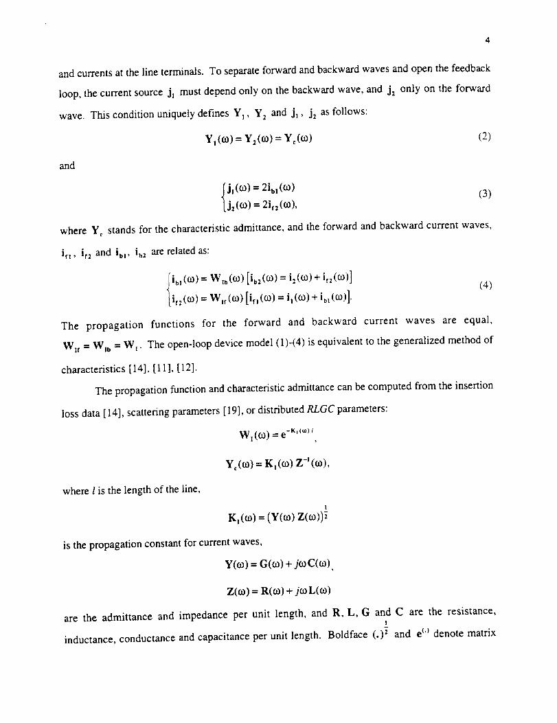
andcurrentsatthe line terminals.To separateforwardandbackwardwavesandopenthefeedback
loop, thecurrentsourceJl mustdependonly on thebackwardwave,and J2only on theforward
wave. This condition uniquely defines YI, Y2 and Jl, J2 as follows:
Y1 (t9) = Y_ (co) = Y¢ (co) (2)
and
Jl (_) = 2ibl (CO)j2 (O,))= 2if_ (O.)), (3)
where Yc stands for the characteristic admittance, and the forward and backward current waves,
ir_, if2 and ibm, ibz are related as:
ib, (03) = Wlt,(C0) [ib2(03) = i:(t0)+ ir2(_) ]it:(co) W,f(co)[it,(co) = i,(co)+ ib,(o3) ]. (4)
The propagation functions for the forward and backward current waves are equal,
Wit = Wn, = Wt. The open-loop device model (1)-(4) is equivalent to the generalized method of
characteristics [14], [1 1], [12].
The propagation function and characteristic admittance can be computed from the insertion
loss data [14], scattering parameters [19], or distributed RLGC parameters:
Wl (0,)) = e-K, _t°_l
Y_(co) = K1(o3) Z-J(o_),
where I is the length of the line,
I
Kt (o)) = (Y(_o) Z(o)))i
is the propagation constant for current waves,
Y(co) = G(co) + jco C(co),
Z(co) = R(co) + jco L(co)
are the admittance and impedance per unit length, and R, L, G
inductance, conductance and capacitance per unit length.
and C are the resistance,!
Boldface (.)i and e_') denote matrix

5
square root and matrix exponential, respectively.
III. DIFFERENCE APPROXIMATION
To perform the transient analysis, indirect numerical integration is applied to the propagation
functions and characteristic admittances in the frequency-domain line model (1)-(4) by using the
difference approximation method,
For the difference approximation in the parallel canonic form, samples of the frequency-
domain transfer function are approximated with the rational polynomial function
M 1IT.I(jco) = I2I + y. (5)
,7"o--l + jo3 / c%. Am'
or samples of the time-domain unit-step response are approximated with the exponential series
M
h(t) = I7to - Z e-°""A,,,,m=l
where 17-1oand I7t. denote the initial and final values of the approximating transfer function
Once the approximation has been performed, indirect numerical integration formulas
(discrete-time difference equations) are readily given in terms of the approximation parameters.
For the step invariance the formulas are
M
y(t.)=H.x(t.)+Zzm(t.)m=l
Zm(t.)= (1-e -o*.r" )A mx(t._,)+ e -_*"r" Zm(t._,),
(6)
where x, y and z,. stand for the excitation, response and state variables, respectively, and
7". = t. - t._ L is the time step at the nth transient iteration.
For the ramp invariance
y(t.) - I_Iox(t.) - ___1z,. (t.) _,
z.,(t.)=D.,(T.)(x(t.)-x(t. ,))+e- ' .r. Zm (t._j) '
(7)
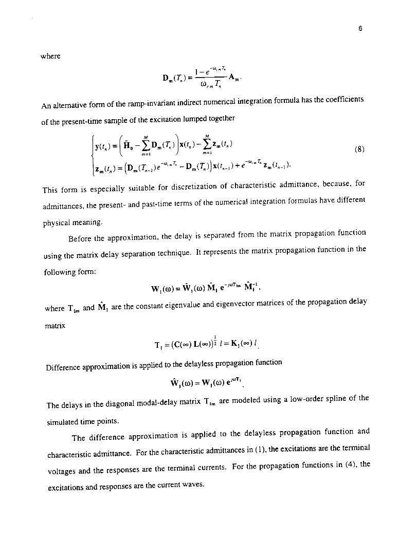
where
l --e - _'" T.
D,,, (T_) = A m.0_,. r,, T,,
An alternative form of the ramp-invariant indirect numerical integration formula has the coefficients
of the present-time sample of the excitation lumped together
This form is
y(t.)= I_Io - D_(T_) X(t.)--_Zm(t.)m=]
[z,,, (t,,)--(Dm(T._,)e -_''r" - Dm(T.))x(t,_,)+ e -°'''r" z,,, (,._,).
(8)
especially suitable for discretization of characteristic admittance, because, for
where Tim
matrix
Before the approximation, the delay is separated from the matrix propagation function
using the matrix delay separation technique. It represents the matrix propagation function in the
following form:
W,(03) = "v_/,(_) 9¢I, e --''''T'' IQI_",
and 1VII are the constant eigenvalue and eigenvector matrices of the propagation delay
!
T, = (C(oo) L(_))i l = K, (oo) l
Difference approximation is applied to the delayless propagation function
_Vl(fD)= Wt(_ ) e -/°:r,
The delays in the diagonal modal-delay matrix Tim are modeled using a low-order spline of the
simulated time points.
The difference approximation is applied to the delayless propagation function and
characteristic admittance. For the characteristic admittances in (1), the excitations are the terminal
voltages and the responses are the terminal currents. For the propagation functions in (4), the
excitations and responses are the current waves.
physical meaning.
admittances, the present- and past-time terms of the numerical integration formulas have different

Since the open-loop functions are aperiodic, they have to be approximated with only real
poles, -c0c, _ . In addition, the poles have to be negative to assure stability.
To represent the original functions accurately with the minimum number of samples, the
variation of the original function from sample to sample should be about the same. The following
empirical formula for the sampling frequencies was found to provide good results
o3_ = 03K(1-cosnk_, k =0, 1,.. K.2K) '
The end of the approximation interval, 6%:, should be chosen so that the original function would
closely approach its final value. This assures that the resulting indirect numerical integration
formulas will be accurate in the full frequency and time ranges from zero to infinity.
IV. MATRIX COMPLEX RATIONAL APPROXIMATION
METHOD FOR FREQUENCY-DOMAIN DIFFERENCE
APPROXIMATION
The method fits samples of an N x N complex matrix transfer function H(O3) with the rational
polynomial function (5) at the set of arbitrary spaced frequencies {0, o3f, o3, ..... cox }. The method
proceeds in three steps.
First, the real part of the sum of the elements of the original matrix function,
N N
i:l j=]
is fit with the real part of the complex rational polynomial function, which is a real rational
polynomial function of squared frequency
Re(ftz(jo3))= Co +c, CO2 +c2(O32) 2 +...+cM (O32) M1 + 13,o32 + 132(o32)2 +... + 13u (o32)u" (9)
The following linear system of equations results from matching the real part of the original function
with (9) at the set of frequencies and premultiplying both sides of each equation with the
denominator

Ii 0 ... 0
co_ ... o_M
2 2M
(OK "'" (OK
0
-(o_ Re(H_:((O,))
: Re(Hr((ox))--(O K
Co
... 0 t "
... _(O_u Re(HI((O'))I cu• -_-
... _(o M__3g
Re(H_(O)) ]
Re(Hz((OK ))J
(10)
For interpolation, K = 2M and solving (10) produces a rational polynomial function which
coincides with the real part of the original function at all of the sampling points. For a set of
samples larger than 2M+I, the least square solution of the system (10) can be obtained.
However, it minimizes the approximation error premultiplied with the denominator, which can lead
to inaccurate approximation. Better results are achieved with the method of averages [21], which
partitions the larger number of equations into 2M + 1 subsets in order of the increasing of co. The
equations within each subset are added up, which makes the system consistent. The method is
effective in averaging out the noise in measured data.
After the real part has been approximated, the denominator of (9) is factored yielding the
2squared poles, -coo, .. Consequently, no unstable right-half-plane poles can be produced•
However, there still can be spurious complex conjugate and purely imaginary poles, which are
removed• The remaining real negative poles are used to formulate the equations for the partial
expansion coefficients, A m, of (5). As a result, the order M of (5) is less or equal to that of (9).
Matching the real and imaginary parts of each element of the original matrix transfer
function H(co) with the corresponding parts of elements of (5) at the set of frequencies
{0, to_, 602..... _Jc } leads to the following linear systems of equations

A __
-I 1 ... 11 1
11 + _ / co_, 1 + co_ / t.o_M
1 I
1 1+0 -(.Oj / t.O_j -t.Oj / _
"_ 2 ''"
1 + co? /coc_
0
1 + col Ico_
-co K/COcj -to K/co_
I + co_.lo)z_ I + o.)_.Io)_
In.l,,
[A,Lx-[A,],j =b=
[H(0)] o
Re([H(co,)]o)
Re([H(cor )],j)
(I1)
For interpolation M = 2K, and both real and imaginary parts of the original transfer function are
matched exactly at all of the K frequency points and dc. For an arbitrary larger number of points,
the least square solution of 11) is obtained from
ArAx = Arb.
The total computational complexity of the approximation method is that of N: + 1 real
linear solutions and one polynomial factoring. The orders of the polynomial and linear systems
depend only on the order of the approximation and not on the number of the original function
samples. Since no iterative or relaxation techniques are involved, the method is free from
convergence problems•
Fig. 2 shows an example of the fourth-order approximation of an open-loop transmission-
line transfer function• As can be observed, although only nine samples of the original function
were used, the approximation exhibits an excellent match in the full frequency range. In general,
due to their simplicity, the open-loop functions can be accurately fit with the 3rd-9th-order
approximation.
V. COMPANION MODEL
By applying the difference approximation to the propagation function and characteristic admittance,
the frequency-domain elemen! characteristic (1) is transformed into the following discrete-time
element characteristic, or companion model

10
i, (t.) = '_', (t.) v,(to)- j,(t.)i:(t.) = '_2(t.) v_(t,)- j,(t,).(12)
The circuit-diagram interpretation of the companion model is shown in Fig. 3.
The admittances _'z and _"2 represent present-time coefficients in the indirect numerical
integration formulas for the admittances Y, and Y2" The current sources j, and ]z combine the
currents Jr, and Jr, corresponding to the remaining parts of the numerical integration formulas for
the admittances, and j, and Jz which are given by the discretized Eqs. (3) and (4)
(13)
Eqs. (3) and (4) do not contribute to the admittance part of the companion model because the
propagation functions contain a delay.
The Modified Nodal Approach (MNA) stamp corresponding to the companion model (12)
is:
KCL at
node:
1.1
I.N
2.1
2.N
2'
VL, ... Vt_, V I.
N
-2[_,],,l=l
,%,
]zl.... "-X' -- _ _'-_ "'_
-2[';', l, .... YT_,],,_i2Y_[_',],,t=l izl I I=l 3=1
V2I •.. V2. N
III
If
-2[_'21,_.... 2['_,],,,
7 2 •
-T_.[_2],,ltl
N
-Y.[_',]_,)m|
V2,
[J,],
-- -y[j,],m ,
[],],
IJ_]N
-_[_],r=l
(14)
In the circuit simulator during the transient analysis, the lines are represented by the tables of
numbers (14) which are recursively updated at each time iteration using numerical integration. The
left-hand side of the stamp (14) has to be updated only when the value of the time step changes. If

11
the step-invariant indirect numerical integration formulas (6) are used, the left-hand side of the
stamp becomes independent of the time step, and only the right-hand side vector has to be updated.
Since the terminal currents are not introduced as variables, the values of i I and i z in (4) are
computed from (12).
VI. LINE MODEL FOR AC AND DC ANALYSES
For ac and dc analyses, the complexity of the transfer functions is not important, and the element
characteristic which does not require the introduction of current variables and is suitable for the
ac/dc modeling of transmission lines is the Y-parameter characteristic
i, {¢o) = Y. (o_) v, (o_) + Y12 (o_) v: (o_)i_(_) Y_,(0J) vl(o_)+Y22(03) v:(03). (15)
The Y-parameters are related to the open-loop functions as follows
Y,, (o3) = Y22(eo) = Y_(¢o) + 2[I- W_ ((o)]-1W_(co)Y¢(o3),
Y12(CO) Y,I(CO) -2[I _ -1= . = -Wl(0_)] Wl(°3)Yc(w), (16)
where I is the identity matrix. The expressions were derived by eliminating jj and J2 from Eqs.
(1)-(4), and transforming them to the form of (15).
The dc model is merely the ac model at zero frequency. For the limiting case of lines with
zero distributed conductance, G = 0, the dc values of the Y-parameters are
Y,, (0) = Y22 (0) = -Y,_ (0) = -Y_I (0) = 1 R_l.1
The MNA stamp corresponding to (1 5) is
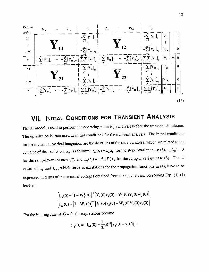
12
KCL atV_f
node:
1.1 II
VIA :
Vz._:
Vr Im
V,.2
V,.N
V 2
0
= 0
0
0
0
(16)
VII. INITIAL CONDITIONS FOR TRANSIENT ANALYSIS
The dc model is used to perform the operating-point (op) analysis before the transient simulation.
The op solution is then used as initial conditions for the transient analysis. The initial conditions
for the indirect numerical integration are the dc values of the state variables, which are related to the
dc value of the excitation, x 0 , as follows: z,,(to) = a,,x o for the step-invariant case (6), z_(t o) = 0
for the ramp-invariant case (7), and z,,(to)=-d,,(T t)x o for the ramp-invariant case (8)• The dc
values of i n and ib2, which serve as excitations for the propagation functions in (4), have to be
expressed in terms of the terminal voltages obtained from the op analysis. Resolving Eqs. (1)-(4)
leads to
I 2 -I
ir,(O)=[I- W,(O)] [Y,(O)v,(O)-W,(O)Y=(O)vz(O)]
2 -I
[ib,(O) [I-W,(O)] [Yc(O)v,(O)-Wt(O)Y,(O)v,(O)].
For the limiting case of G = O, the expressions become
_,,(o)= -k,(o) = _ R-'[v, (o)- v2(O)].

VIII. SIMULATION ALGORITHM
For an MNA-based simulator, the line simulation algorithm is as follows.
13
1. Before the transient analysis:
a) Perform op analysis of the circuit to find the initial conditions for the transient analysis.
Use the ac/dc model ( 15)-(16).
b) For each line in the circuit, perform the difference approximation of each element of the
propagation function and characteristic admittance matrices.
2. At each time iteration:
Recursively update the line stamps using the indirect numerical integration formulas
obtained at step 1(b) and companion model ( 12)-(14).
Since the method introduces neither additional nodes nor current variables, the line
modeling does not increase at all the circuit solution time. The only additional time is required to
perform a low-order interpolation once in the beginning of the simulation, and for a low-order
numerical integration. As shown in the next section, this time is negligibly small compared to the
circuit solution time.
IX. NUMERICAL RESULTS
The method has been adopted in several industrial and commercial circuit simulators, and, in
numerous real-life simulation exercises, proved to be reliable, accurate and efficient. Table II
presents relative runtime data for circuits of various types and sizes. As can be observed, even for
the worst case of a small circuit consisting of lines only, the model is virtually as efficient as the
simple replacement of interconnects with lumped resistors. The resistive model was chosen for the
comparison because it represents the limiting case in the simplicity and computational efficiency of
the interconnect modeling.
Fig. 4 verifies the method's accuracy with Spice3e2 lossy multiconductor line model [8].
A simple network was chosen as an example to reduce the influence of factors other than the line
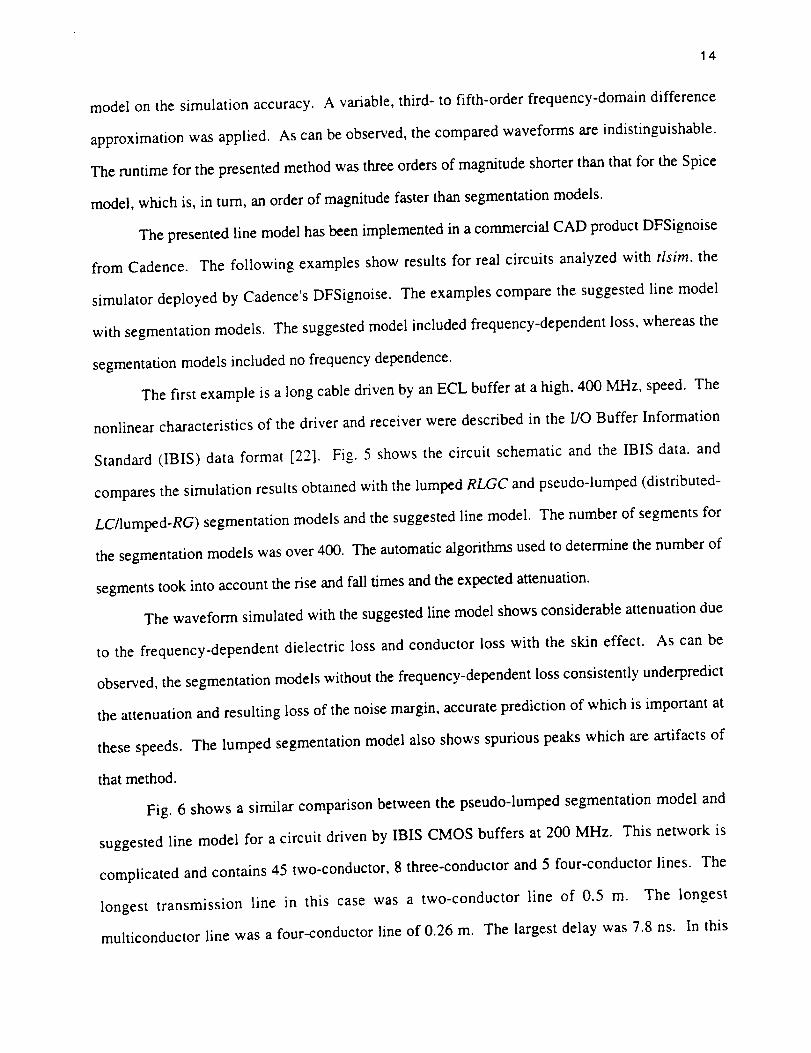
14
model on the simulation accuracy. A variable, third- to fifth-order frequency-domain difference
approximation was applied. As can be observed, the compared waveforms are indistinguishable.
The runtime for the presented method was three orders of magnitude shorter than that for the Spice
model, which is, in turn, an order of magnitude faster than segmentation models.
The presented line model has been implemented in a commercial CAD product DFSignoise
from Cadence. The following examples show results for real circuits analyzed with tlsim, the
simulator deployed by Cadence's DFSignoise. The examples compare the suggested line model
with segmentation models. The suggested model included frequency-dependent loss, whereas the
segmentation models included no frequency dependence.
The first example is a long cable driven by an ECL buffer at a high, 400 MHz, speed. The
nonlinear characteristics of the driver and receiver were described in the I/O Buffer Information
Standard (IBIS) data format [22]. Fig. 5 shows the circuit schematic and the IBIS data. and
compares the simulation results obtained with the lumped RLGC and pseudo-lumped (distributed-
LC/lumped-RG) segmentation models and the suggested line model. The number of segments for
the segmentation models was over 400. The automatic algorithms used to determine the number of
segments took into account the rise and fall times and the expected attenuation.
The waveform simulated with the suggested line model shows considerable attenuation due
to the frequency-dependent dielectric loss and conductor loss with the skin effect. As can be
observed, the segmentation models without the frequency-dependent loss consistently underpredict
the attenuation and resulting loss of the noise margin, accurate prediction of which is important at
these speeds. The lumped segmentation model also shows spurious peaks which are artifacts of
that method.
Fig. 6 shows a similar comparison between the pseudo-lumped segmentation model and
suggested line model for a circuit driven by IBIS CMOS buffers at 200 MHz. This network is
complicated and contains 45 two-conductor, 8 three-conductor and 5 four-conductor lines. The
longest transmission line in this case was a two-conductor line of 0.5 m. The longest
multiconductor line was a four-conductor line of 0.26 m. The largest delay was 7.8 ns. In this

15
case,thetwo modelsproducedcomparableresults,sincetherise time of the driver was0.9 nsas
opposedto the0.3ns of theECL driver. Thefigure alsoshowsthecrosstalkwaveform V_. The
crosstalk waveforms for the suggested and segmentation models were very close.
X. CONCLUSIONS
This paper presented a method for circuit simulation of uniform multiconductor lossy frequency-
dependent lines characterized by sampled frequency-domain responses. The method uses element
characteristics which do not require the introduction of current variables, simple open-loop
transmission line characterization, matrix indirect numerical integration formulas, hove] direct
matrix rational approximation method, and novel matrix delay separation technique. The complete
step-by-step implementation of the method was presented, including ac, dc and transient analyses.
extraction of initial conditions from the op analysis, and MNA stamps.
The method is compatible with recursive time-domain solvers employed by circuit
simulators and supports variable time-stepping. The method has been adopted in several industrial
and commercial circuit simulators, and, in numerous real-life simulation exercises, proved to be
reliable and accurate. It was shown on an extensive set of runtime data that the method is as
efficient as simple replacement of interconnects with lumped resistors.
ACKNOWLEDGMENT
The authors wish to thank Mr. H. Satsangi for installing the presented line model in Spice, and Dr.
R. Wang for implementing the model in the circuit simulator at Intel.
[11
REFERENCES
T. Dhaene, L. Martens and D. De Zutter, "Transient simulation of arbitrary nonuniform
interconnection structures characterized by scattering parameters," IEEE Trans. Circuits
Syst., vol. 39, pp. 928-937, Nov. 1992.

[2]
[3]
[4]
[5]
[6]
[7]
[8]
[9]
[IO]
[11]
[12]
16
Syst., vol. 39, pp. 928-937, Nov. 1992.
J. E. Bracken, V. Raghavan and R. A. Rohrer, "Interconnect simulation with asymptotic
waveform evaluation (AWE)," IEEE Trans. Circuits Syst., vol. 39, pp. 869-878, Nov.
1992.
T. Dhaene and D. De Zutter, "Selection of lumped element models for coupled lossy
transmission lines," IEEE Trans. Computer-Aided Design, vol. 1 I, pp. 805-815, Jul. 1992.
K. S. Oh and J. E. Schutt-Aind, "Transient analysis of coupled, tapered transmission lines
with arbitrary nonlinear terminations," IEEE Trans. Microwave Theory Tech., vol. 41, pp.
268-273, Feb. 1993.
J. E. Schutt-Ain6 and R. Mittra, "Nonlinear transient analysis of coupled transmission
lines," IEEE Trans. Circuits Syst., vol. 36, pp. 959-967, Jul. 1989.
I. Maio, S. Pignari and F. Canavero, "Influence of the line characterization on the transient
analysis of nonlinearly loaded lossy transmission lines," IEEE Trans. Circuits Syst., vol.
41, pp. 197-209, Mar. 1994.
F. Romeo and M. Santomauro, "Time-domain simulation of n coupled transmission lines,"
IEEE Trans. Microwave Theory Tech., vol. MTT-35, pp. 131-137, Feb. 1987.
J. S. Roychowdhury and D. O. Pederson, "Efficient transient simulation of lossy
interconnect," in Proc. 28th ACM/IEEE Design Automation Conf., 1991, pp. 740-745.
F.-Y. Chang, "Transient analysis of lossy transmission lines with arbitrary initial potential
and current distributions," IEEE Trans. Circuits Syst., vol. 39, pp. 180-198, Mar. 1992.
F. H. Branin, Jr., "Transient analysis of lossless transmission lines," Proc. IEEE, vol. 55,
pp. 2012-2013, Nov. 1967.
F.-Y. Chang, "Transient simulation of nonuniform coupled lossy transmission lines
characterized with frequency-dependent parameters, Part I: Waveform relaxation analysis,"
IEEE Trans. Circuits Syst., vol. 39, pp. 585-603, Aug. 1992.
F.-Y. Chang, "Transient simulation of frequency-dependent nonuniform coupled lossy
transmission lines," IEEE Trans. Components Packaging Manufacturing Technology, vol.
17, pp. 3-14, Feb. 1994.
[13]
[14]
[15]
[16]
[17]
[181
[19]
[20]
[211
[22]
17
J. E. Bracken, V. Raghavan and R. A. Rohrer, "Extension of the asymptotic waveform
evaluation technique with the method of characteristics," Tech. Dig. IEEE Int. Conf.
Computer-Aided Design, 1992, pp. 71-75.
A. J. Gruodis and C. S. Chang, "Coupled lossy transmission line characterization and
simulation," IBMJ. Res. Develop., vol. 25, pp. 25-41, Jan. 1981.
A. Semlyen and A. Dabuleanu, "Fast and accurate switching transient calculations on
transmission lines with ground return using recursive convolutions," IEEE Trans. Power
Appar. Syst., vol. PAS-94, pp. 561-569, Mar./Apr. 1975.
T. K. Tang, M. S. Nakhla and R. Griffith, "Analysis of lossy multiconductor transmission
lines using the Asymptotic Waveform Evaluation technique," 1EEE Trans. Microwave
Theory Tech., vol. 39, pp. 2107-2116, Dec. 1991.
C. R. Paul, "On uniform multimdde transmission lines," IEEE Trans. Microwave Theor?,,
Tech., pp. 556-558, Aug. 1973.
L. T. Pillage and R. A. Rohrer, "Asymptotic waveform evaluation for timing analysis,"
1EEE Trans. Computer-Aided Design, vol. 9, pp. 352-366, Apr. 1990.
J. E. Schutt-Ain6, "Modeling and simulation of high-speed digital circuit interconnections,"
Ph.D. dissertation, University of Illinois at Urbana, 1988.
D. B. Kuznetsov and J. E. Schutt-Ain6, "Optimal transient simulation transmission lines,"
accepted for publication in 1EEE Trans. Circuits Syst..
I. N. Bronshteyn and K. A. Semendyaev, Spravochnik po matematike. Moscow: Nauka,
1967, p. 578. In Russian.
D. Duehren, W. Hobbs, A. Muranyi and R. Rosenbaum, "I/O-buffer modeling spec
simplifies simulation for high-speed systems," Electronic Design News (EDN), p. 65, Mar.
1995.
18
Fig. 5.
Fig. 6.
FIGURE CAPTIONS
Conventions for the voltages and currents at the line terminals.
An example of the 4th-order complex rational approximation. The original function is
shown by the thin continuous curves and the approximating function by the thick dashed
curves.
Companion model for a transmission line.
(a) the network configuration and (b) comparison of the transient waveforms generated
using the line model installed in an MNA-based circuit simulator (thick broken curves)
and Spice3e2 (thin continuous curves). R_=Rs=50 _, R2=R6=l kf2, R3=R4=10 Mr2;
self-inductance L,=418 nil/m, self-capacitance C,=94 pF/m, mutual inductance L,,= 125
nil/m, mutual capacitance C,,,=22 pF/m, R=15 f2/m, G=O, l=0.677 m (all signal
conductors are the same).
(a) the circuit schematic, (b) IBIS model for the ECL buffers, and (c) the transient
waveforms simulated with the segmentation and suggested line models. The line
parameters are: L=502 nil/m, C=67.9 pF/m, R={3.25 f2/m at de, 87.7 f2/m at 10
GHz}, G={430 fS/m at dc, 4.3 mS/m at 10 GHz},/=0.88 m.
(a) the circuit block schematic, (b) IBIS model for the CMOS buffers, and (c) the
transient waveforms simulated with the segmentation and suggested line models.
Table I. Relative runtimes.
TABLE CAPTIONS
FOOTNOTES
Manuscript received
This work was supported by NASA under the grant NAG 2-823, and by the Office of Naval
Research Joint Services Program under the grant N00014-90-J-1270.
The authors are with the Department of Electrical and Computer Engineering, University of

19
Illinois, Urbana, IL 61801, USA.

[ill__.2 [vl] I1.1 °
[ill____2[vl] 2!.2 "
m
l'm
N+ l-conductor line
T
Signal
conductors| •
Reference conductor
IJ ..l
[v2] I [i2]__._[I'2.1
[v2] 2 [i2]____2J '2.2
[v21u [i2]u_' 2.N
+
- ,2'
Fig. 1

0.00376
= 0.00374
E
<.2 0.00372
= 0.0037
0
= 0.00368
0.00366
0
f
, . . k ] s J 1 I
50 100 150 200 250 300
Frequency, co (Mrad/s)

0.01
0.005e-,
.m
E"_ 0<
-0.005
-0.01_9
r-
-0.015
t.
0 50 100 150 200
Frequency, co (Mrad/s)
i
250 3_
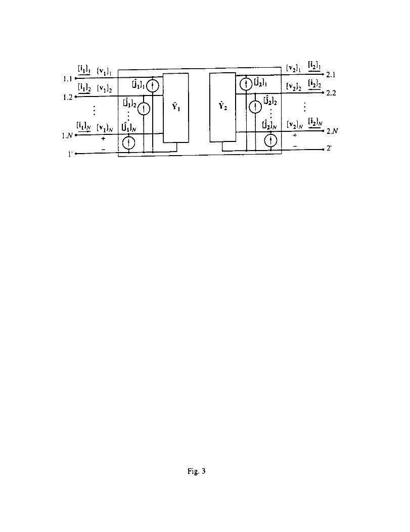
[i11_ [vl] I1.1 •
[il]2 [vl]21.2 •
m
Ei,]l /
[v2] 1 [i2]..__]1'2.1
Ivy]2 [i21..__2• 2.2
[v2]_' 2.N+
•....-..-_-....._..-_2'
Fig. 3
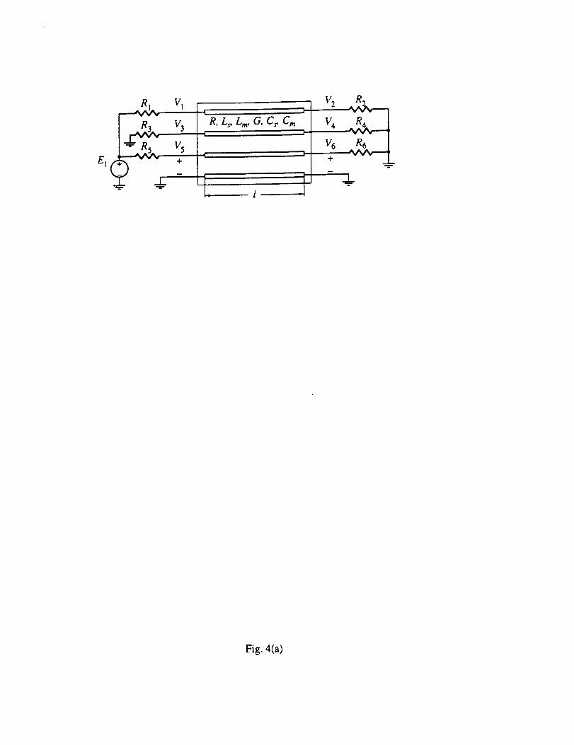
E 1
R V 1
V3
VS+
R, Lr L m, G, C s, C m
R6
Fig. 4(a)
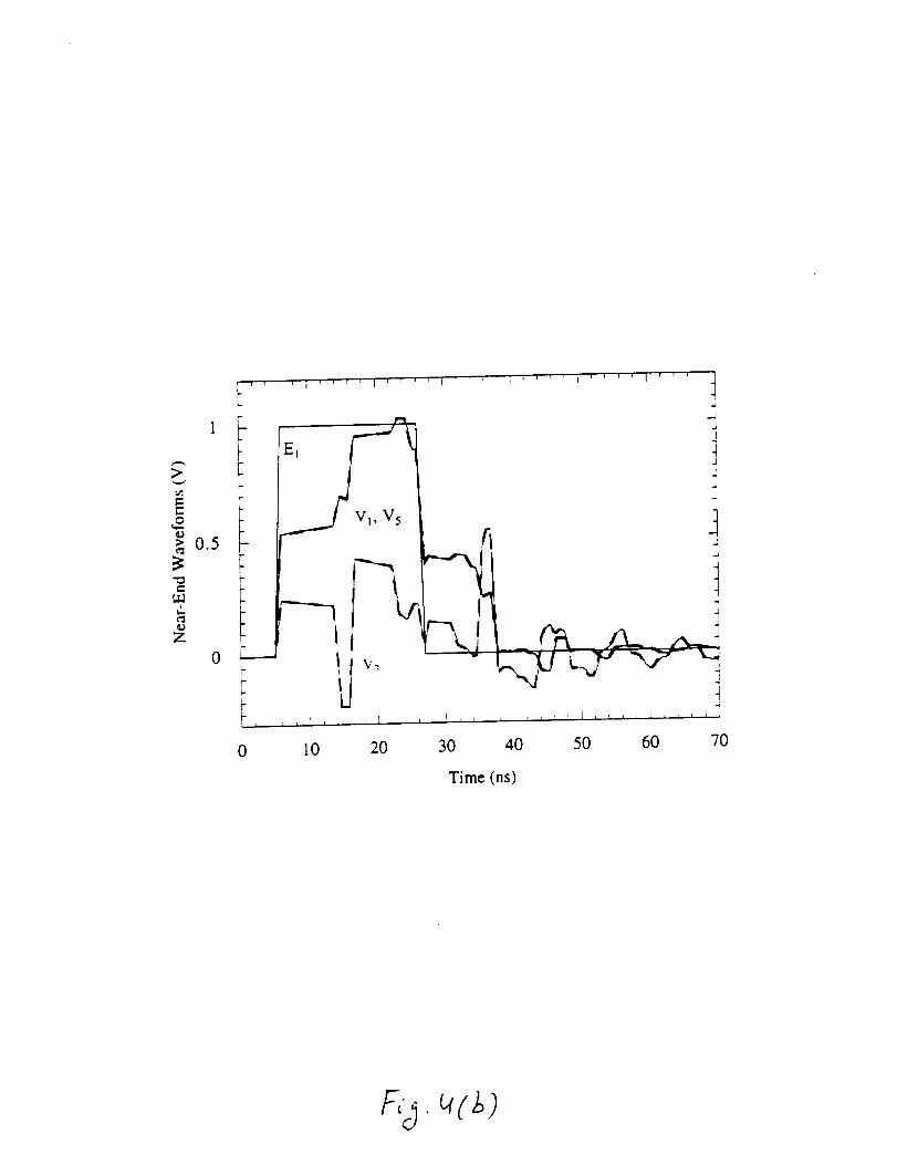
V"
¢dl
> 0.5
c
Z
0
0 10 20 30 40 50 60 70
Time (ns)

v D- 50..1.-
Fig. 5(a)

>,....,.,
EL.,
C
,j
=_
'.,C.+-
F...
-0.8
-1.0
-1.2
-1.4
-1.6
Lumped_,t segmentation
model
Suggestedmethod
Pseudo-lumpedsegmentation model
40 41 42 43 44 45
Time (ns)
Fig. 5(c)
.<
-'-1
L)
e_
©
0.00
-0.10-2
down
f/
/I
I
I
/ Pull-upI
I!
I
-1
Output Voltage (V)
O
Fig. 5(b)

Fig. 6(a)

0.3
<
e,.
¢-,w
G
0.2
0.1
0.0
-0.1
-0.2
-0.3
Pull-down
Ground
stSS / / j 7
s a
s t
st 4
f
-5 0 5
/
,'_"_ Power
clamp
10
Output Voltage (V)
Fig. 6(b)

J
>,
e-.
c
.N
Z
[.-.
6
,4
2
0
-2
70
V2, segmentation model
72 74 76
Time (ns)
78 8O
Fig. 6(c)

"_ @ ,tJ ,-- -_
_ _ .£
_ -=_z__
,-,1
,,,ID
._=_._ ._
.&L.
.N
rj
Z Z
;. ,_. ?
_ 7a
'-£8 _o=
O
_7
0 m
M