high-k dielectrics in nanoµelectronics - romnet · the paper presents enhancements in this...
TRANSCRIPT

High-K Dielectrics in Nanoµelectronics
G. Brezeanu1, M. Brezeanu2, F. Bernea3 1University “POLITEHNICA” Bucharest, Splaiul Independentei 313, 040011, Bucharest, Romania
2Engineering Department, University of Cambridge, 9 JJ Thomson Avenue, Cambridge CB3 0FA, UK 3Carpatcement Holding, Romania
Abstract. For CMOS applications, as device scaling, obeying Moore’s law reduces the active area of the devices to nearly atomic dimensions. The high-k dielectrics need to be used to prevent the tunnelling effects which increase the leakage currents. These insulators are also important for enabling high-performance nanoelectronic transistors built on high-mobility materials, such as diamond, carbon nanotubes or silicon carbide (SiC). One of the major issues to be addressed when coming to power devices is the choice of the appropriate termination. An already, classical implementation of the field plate technique, widely used for Si, SiC and diamond power diodes, is the oxide ramp termination. This method requires the presence of a dielectric ramp smaller than 10º, etched around the anode, which assures the smoothness of the electric field at the contact’s periphery. The main limitation of this termination is a premature oxide breakdown which is a killing factor for the yield. The paper presents improvements in the efficiency of this termination for Schottky Barrier Diodes (SBDs) on SiC and diamond, using high-k dielectrics. These insulators can reduce both the oxide and the surface semiconductor electric field.
Introduction
In recent years, several emerging high-k materials have attracted enormous attention as potential candidates for electronic devices. Silicon dioxide (SiO2) has been used as dielectric for more than 40 years because of its manufacturability and ability to deliver continued transistor performance improvements as it has been made ever thinner [1-10].
Over decades of incremental improvements to CMOS processing, the limitations of the SiO2 gate dielectric layer have hung over the silicon industry as its single biggest technical challenge [1-15].To improve MOS transistor performance in the past, chip manufacturers have shrunk the thickness of the gate dielectric to as little as five atomic layers (1.2 nm). Although this has helped transistors reach very high speeds, the problem is that these very thin layers of SiO2 tend to leak a lot of current, resulting in energy waste and a build-up of heat. In addition, SiO2 thickness uniformity across a 12 inch wafer imposes even more crucial difficulty in the growth of such a thin film, since even a mono-layer difference in thickness represents a large percentage difference and thus can result in the variation of threshold voltage across the wafer [4]. Reliability also becomes a huge concern for a very thin layer SiO2 film.
Intel have been integrated into a manufacturable 45nm process a combination of a high-k dielectric based on hafnium and a new metal gate material compatible with hafnium will reduces source-drain leakage substantially [1,9-10]. Gordon Moore described this new approach, as the "biggest change in transistor technology since the introduction of polysilicon gate MOS transistors in the late 1960s"[10].
IBM has come up with a slightly different solution to the leakage problem, but is also using a high-k dielectric gate, [10].The latest developments at Intel and IBM will help III-V devices penetrate new markets, by instigating greater convergence of the compound and silicon industries. High-k dielectric is at the centre of this, and high-k compound semiconductor MOSFETs will be able to leverage the millions of man years of silicon circuit designs, [10].
Actually, there is an increasing interest in the use of wide band-gap semiconductors, such as silicon carbide (SiC) and diamond, for power switching, power conversion, motor drives and military and consumer electric vehicles [16-22]. An issue related to the design of SiC or diamond devices is the junction discontinuity at the sharp corners of the electrodes. These results in noticeable increase of the maximum electric field in semiconductor bulk compared with its one dimensional value. These field peaks can be reduced using edge terminations surrounding the electrodes periphery [16-17]. Field plate termination is widely used in power devices design due to a less complicated fabrication process. We proposed and already tested on Si, SiC and diamond diodes a simple, low temperature, field plate termination based on a small angle etching of a dielectric deposed around the anode contact [18-22].
The paper presents enhancements in this termination for Schottky barrier diodes (SBDs) on SiC and diamond, using high-k dielectrics. The use of high-k materials allows for the reduction of the electric field at the corner by minimizing the recess without losing electrode control. Scaling limits of SiO2
The prosperity of modern integrated circuits has been realized with continuous shrinkage of MOS transistors
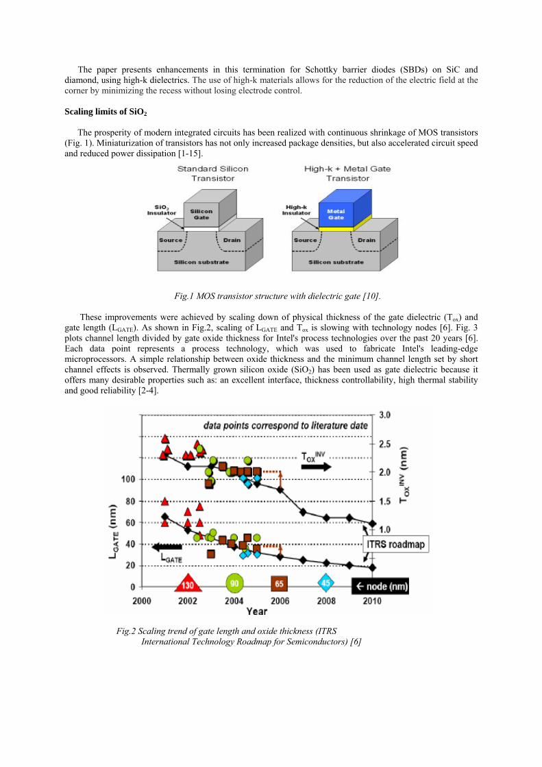
(Fig. 1). Miniaturization of transistors has not only increased package densities, but also accelerated circuit speed and reduced power dissipation [1-15].
Fig.1 MOS transistor structure with dielectric gate [10].
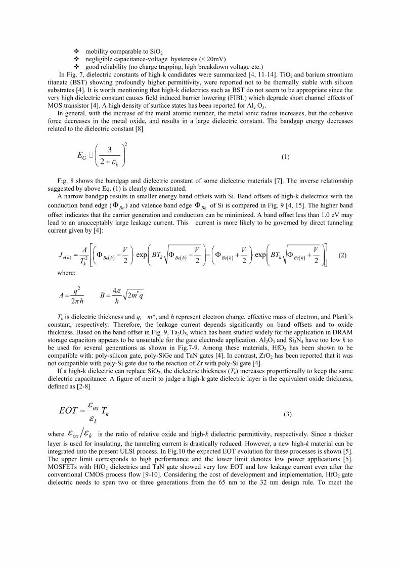
These improvements were achieved by scaling down of physical thickness of the gate dielectric (Tox) and gate length (LGATE). As shown in Fig.2, scaling of LGATE and Tox is slowing with technology nodes [6]. Fig. 3 plots channel length divided by gate oxide thickness for Intel's process technologies over the past 20 years [6]. Each data point represents a process technology, which was used to fabricate Intel's leading-edge microprocessors. A simple relationship between oxide thickness and the minimum channel length set by short channel effects is observed. Thermally grown silicon oxide (SiO2) has been used as gate dielectric because it offers many desirable properties such as: an excellent interface, thickness controllability, high thermal stability and good reliability [2-4].
Fig.2 Scaling trend of gate length and oxide thickness (ITRS International Technology Roadmap for Semiconductors) [6]

Fig. 3. Channel length to gate oxide thickness ratio versus
channel length for some Intel process technologies [6]
For new CMOS nanotechnology (LGATE< 90nm) SiO2 has reached its physical limitations: higher leakage current and reliability concerns. A physical thickness of 11-15Å is so thin that electrons can directly tunnel through the oxide, resulting in excessively high gate leakage current. The forecasted leakage current is shown in Fig.4 [5]. High leakage is a great concern, particularly for low power requests, and high performance applications as well. Due to the increase in the gate leakage, static power can exceed the active power as shown in fig. 5, [6]. To reduce the increase in active power, VDD needs to be reduced as well.
But as seen in fig. 6 [6], VDD is also falling behind the roadmap targets thus limiting the reduction of active
power and increasing the electric field across the gate oxide, which decreases the reliability of the gate oxides.
Fig. 4 The predicted range of acceptable gate leakage current over the years; the upper limit represents high
performance and the lower limit represents low power applications [5]

Fig.5 Active and static power increase with scaling of LGATE
Fig. 6. Scaling of VDD with technology nodes [6]. High-k dielectrics High-k gate dielectrics have been studied as alternative gate dielectrics for the 65nm CMOS technology
(Fig.1) and beyond to replace conventional SiO2 or silicon oxynitrides (SiOxNy). The requirements for high-k dielectric applications are [5]:
high dielectric constant and large band gap high band offset with electrodes thermally and chemically stable in contact with semiconductor substrate scalable equivalent oxide thickness EOT < 10Å compatibility with gate electrode material density of interface states comparable to SiO2 low lattice mismatch and similar thermal expansion coefficient with Si
mobility comparable to SiO2 negligible capacitance-voltage hysteresis (< 20mV) good reliability (no charge trapping, high breakdown voltage etc.)
In Fig. 7, dielectric constants of high-k candidates were summarized [4, 11-14]. TiO2 and barium strontium titanate (BST) showing profoundly higher permittivity, were reported not to be thermally stable with silicon substrates [4]. It is worth mentioning that high-k dielectrics such as BST do not seem to be appropriate since the very high dielectric constant causes field induced barrier lowering (FIBL) which degrade short channel effects of MOS transistor [4]. A high density of surface states has been reported for Al2 O3.
In general, with the increase of the metal atomic number, the metal ionic radius increases, but the cohesive force decreases in the metal oxide, and results in a large dielectric constant. The bandgap energy decreases related to the dielectric constant [8]
23
2Gk
Eε
⎛ ⎞⎜ ⎟+⎝ ⎠
(1)
Fig. 8 shows the bandgap and dielectric constant of some dielectric materials [7]. The inverse relationship
suggested by above Eq. (1) is clearly demonstrated. A narrow bandgap results in smaller energy band offsets with Si. Band offsets of high-k dielectrics with the
conduction band edge ( BeΦ ) and valence band edge BhΦ of Si is compared in Fig. 9 [4, 15]. The higher band offset indicates that the carrier generation and conduction can be minimized. A band offset less than 1.0 eV may lead to an unacceptably large leakage current. This current is more likely to be governed by direct tunneling current given by [4]:
( ) ( ) ( ) ( )( ) 2 exp exp2 2 2 2e h k kBe h Be h Be h Be h
k
A V V V VJ BT BTT
⎡ ⎤⎛ ⎞ ⎛ ⎞⎛ ⎞ ⎛ ⎞= Φ − ⋅ Φ − − Φ + ⋅ Φ +⎢ ⎥⎜ ⎟ ⎜ ⎟⎜ ⎟ ⎜ ⎟⎜ ⎟ ⎜ ⎟⎝ ⎠ ⎝ ⎠⎢ ⎥⎝ ⎠ ⎝ ⎠⎣ ⎦ (2)
where:
2
2qA
hπ= *4 2B m q
hπ
=
Tk is dielectric thickness and q, m*, and h represent electron charge, effective mass of electron, and Plank’s
constant, respectively. Therefore, the leakage current depends significantly on band offsets and to oxide thickness. Based on the band offset in Fig. 9, Ta2O5, which has been studied widely for the application in DRAM storage capacitors appears to be unsuitable for the gate electrode application. Al2O3 and Si3N4 have too low k to be used for several generations as shown in Fig.7-9. Among these materials, HfO2 has been shown to be compatible with: poly-silicon gate, poly-SiGe and TaN gates [4]. In contrast, ZrO2 has been reported that it was not compatible with poly-Si gate due to the reaction of Zr with poly-Si gate [4].
If a high-k dielectric can replace SiO2, the dielectric thickness (Tk) increases proportionally to keep the same dielectric capacitance. A figure of merit to judge a high-k gate dielectric layer is the equivalent oxide thickness, defined as [2-8]
oxk
k
EOT Tεε
= (3)
where ox kε ε is the ratio of relative oxide and high-k dielectric permittivity, respectively. Since a thicker layer is used for insulating, the tunneling current is drastically reduced. However, a new high-k material can be integrated into the present ULSI process. In Fig.10 the expected EOT evolution for these processes is shown [5]. The upper limit corresponds to high performance and the lower limit denotes low power applications [5]. MOSFETs with HfO2 dielectrics and TaN gate showed very low EOT and low leakage current even after the conventional CMOS process flow [9-10]. Considering the cost of development and implementation, HfO2 gate dielectric needs to span two or three generations from the 65 nm to the 32 nm design rule. To meet the

requirements for these generations, EOT should be scaled down to less than 10 while suppressing leakage
current to below 1mA/cm2 (Fig.11), [9]. A combination of a high-k dielectric based on hafnium and a secret new metal gate material compatible with hafnium will cut gate leakage current density by more than 500 times (Fig.11). The dielectric's high k value compensates for the thinning of the dielectric in smaller process geometries. A thinner dielectric enables higher drive and thus allows transistors to switch faster.
Fig.7 Dielectric constant of some high-k dielectrics [4,11-14].
Fig.8 Band gap dependence versus dielectric constant
of some high-k dielectrics [4,11-14

Fig. 9 Band offset of gate dielectric candidates with conduction band edge and valence band
edge of Si substrate [4,15]
Fig. 10 The predicted evolution of equivalent oxide thickness [5]
Fig.11 Nano- MOS structure with high-k dielectric [9]

SiC and diamond electronics devices with high-k dielectrics Wide band gap semiconductors such as diamond and SiC are the promising materials for new power devices.
Over the last two decades, significant advances in the growth, doping, and processing technologies of these materials have been accomplished opening new promise for high power electronics. In real devices, the breakdown voltage of the devices is always less than that predicted by theory, since the material is not perfect (crystal defects) and the electric field is crowding at the electrode corner [16-22].
These high fields can be relieved by using edge termination surrounding the electrode periphery. An effective edge termination makes the electric field distribution uniform in the bulk and at the electrode corner and take the breakdown capability of the device closer to its theoretical limit. Traditionally, techniques like field plates, floating guard rings and junction termination extensions have been used [16-17].
We have already proposed the oxide ramp termination, an original implementation of the field plate concept,
previously widely used for Si, SiC and diamond (Dia) diodes. This termination, shown in Fig. 12 for a Schottky Barrier diode (SBD), is based on a field plate overlapping on oxide ramp at the periphery of the device main electrode contact. The oxide ramp termination is acknowledged by the international community as a highly efficient termination for power devices [16-22]. In this paper, the high-k insulators are used with the ramp oxide termination of SiC and diamond diodes.
Fig. 12 Schottky barrier diode (SBD) with oxide ramp termination For power devices, due to the high voltages employed, the dielectric breakdown might appear before the
semiconductor one. The use of alternative insulators, with high dielectric constants will reduce the electric field within the oxide and, as a consequence, the risk of premature dielectric breakdown. In order to emphasize the effect of varying the relative permittivity (εr) on the performance of ramp oxide terminated structures, extensive simulations were performed on SiC and diamond diodes. In order to avoid dielectric breakdown, the maximum electric field in the oxide (EOX), has to be lower than 5-6MV/cm, acceptable operating fields for high-k dielectrics like Si3N4, Ta2O5 or HfO2 (the later having the highest product between the dielectric constant and the maximum electric field). The increase of εr
not only reduces EOX, but also improves the breakdown voltage (BV) of the diodes. The termination efficiency (η), defined as the ratio between the achieved BV and the ideal one, significantly increases for larger εr, regardless of the ramp angle.
Fig. 13 presents the electric field distribution at the semiconductor surface for both SiC and Dia SBDs, having the same doping level in the drift layer (7x1015cm-3). Two peaks, are observed: one at the beginning and one at the end of the ramp. For both materials, the increase of εr results in a severe reduction of the field peak at the start of the ramp. An increase of the overall electric field at the interface and, a smooth electric field distribution at the Schottky contact and along of the oxide-semiconductor interface can be observed at higher permittivity. This is due to the increase of the voltage drop on the semiconductor when insulators with high permittivity are used.
Consequently, an increase of the termination efficiency is obtained. For SiC SBDs, the efficiency of termination increases strongly with εr, up to 96% (Fig.14). In the case of Dia, the effect of the insulator permittivity is reduced, mainly due to the much lower doping of the drift layer (used in these simulations), and the termination efficiency is around 92%. A mild decrease of the efficiency is observed for high permittivity value.

Fig. 13 Electric field along the interface Dia and SiC SBDs with the same drift doping
Fig.14 Termination efficiency vs. dielectric relative permittivity for SiC and Dia SBDs Another important benefit of the relative permittivity growth is that the ramp angle can be increased up to
100, without affecting the value of the efficiency. This has a direct influence on the area consumption, taking into account the fact that the larger the angle, the smaller the area needed for the termination.
In order to confirm the predictions of the theoretical study presented above, a comparison between the performances of the Schottky diodes, when employing SiO2 and Si3N4 as insulators for the ramp termination, was performed in Fig.15.The ramp angle was kept constant (5.70), while the thickness of the dielectric was varied in the range 0.5-5μm. The Si3N4 ramps show better performances both in terms of termination efficiencies and maximum electric field in insulator (Fig. 15). A very high efficiency of 95% can be obtained for this diode using the silicon nitride for ramp termination (Fig.15a).The fact that η is very high and practically constant with TOX, enables the design to be focused only on reducing EOX, which falls below the acceptable maximum for thicknesses larger than 3.5μm (Fig.15b).

(a) Fig. 15 Comparison between SiO2 and Si3N4 SBDs on SiC from the point of view of
(a) termination efficiency and (b) maximum electric field in the dielectric.
We have also analyzed the impact of using two high-k dielectrics, (Si3N4 and HfO2), as insulators for the ramp termination on diamond Schottky structures (Fig.16). As expected, the electric field in the dielectric decreases at breakdown when using high-k dielectrics (Fig.16b). Values of the maximum dielectric field comparable to the operational field are obtained for HfO2 ramps with insulator thicknesses in excess of 3.5 μm. For these structures, the risk of premature dielectric breakdown is minimum. The price to pay for this improvement in reliability is a small degradation of the electrical performances of the termination. The efficiency drops by 5–7% to 85–87% when using HfO2 instead of SiO2 (Fig.16a), still high enough for a competitive termination structure.
Fig.16 Oxide ramp termination with SiO2, Si3N4 and HfO2 for SBDs on diamond (a) termination efficiency and (b) maximum electric field in the dielectric.
Conclusions The requirement of high performance, high reliability, high package density along with low voltage and low
power application for submicron CMOS technology and device scaling has acted as the driving force. A continuing scaling down of the MOS device with the minimum feature size bellow 90 nm requires EOT less than 15 Å. A physical thickness of only some atomic layers of traditionally gate insulator (SiO2) creates several problems. Electrons can directly tunnel through the SiO2, resulting in excessively high gate leakage current. To solve this critical issue SiO2 has been replaced with a thicker high-k material as HfO2, in the gate dielectric, clamming reduction in leakage by more than two orders of magnitude.
The possibility of using high-k dielectrics for field plate terminations of Schottky on SiC and diamond in order to avoid a possible premature dielectric breakdown was investigated, too.

A high efficiency oxide ramp termination based on high-k insulators has been extensively studied. For SiC SBDs, the efficiency of termination increases strongly with relative permitivity, up to 96%. In the case of Dia, the effect of the insulator permittivity is less significant, and the termination efficiency is around 92%.
With an HfO2 ramp, the premature dielectric breakdown risk can be avoided for dielectric thicknesses larger than 3.5 μm for diamond and SiC Schottky devices. A comparison between SiO2 and Si3N4 ramps for SBDs on SiC showed that the latter exhibits superior performances.
In conclusion, high-k dielectrics are highly recommended for SiC devices, but have a lower impact in the case of low doping diodes on diamond.
References [1] Ann Stafford Muscular,” Intel, IBM embrace high-k metal gates for 45nm” Electronic Weekly,
Jan.2007. [2] R. Agrawal, “Fabrication, Characterization and Hall Mobility Analysis of MOS Devices with Low K and
High K Dielectric Materials”, Thesis for degree of Master of Science in Electrical Engineering , University of Texas at Arlington, 2006. [3] I.Ok, A Study on Electrical and Material Characteristics of Hafnium Oxide with Silicon Interface Passivation on III-V substrate for Future Scaled CMOS Technology” PhD Dissertation, University of Texas at Austin, 2008.
[4] C. Kang, “A study on the material and device characteristics of hafnium oxynitride MOSFETs with TaN gate electrodes”, PhD Dissertation, University of Texas at Austin, 2004.
[5] R. E. Nieh “An evaluation of the electrical, material, and reliability characteristics and process viability of ZrO2 and ZrOxNy for future generation MOS gate dielectric”, PhD Dissertation, University of Texas at Austin, 2002.
[6] M. S. Akbar, “Process Development, Characterization, Transient Relaxation, and Reliability Study of HfO2 and HfSixOy Gate Oxide for 45nm Technology and Beyond”, PhD Dissertation, University of Texas at Austin, 2005.
[7] J. K. Schaeffer, “Hafnium Dioxide Gate Dielectrics, Metal Gate Electrodes, and Phenomena Occurring at their Interfaces “,PhD Dissertation, University of Texas at Austin, 2004. [8] X. Yang , “Issues In Front-End Engineering Of Cmos Nanoelectronics”, PhD Dissertation, University of Texas at Arlington, 2007.
[9] ” High-k Transistor, advanced process technology”, NEC Electronics Corporation , 2005. [10] “IBM and Intel make high-k gate breakthrough”, Compound semiconductor net, 2007. [11] R.D. Shannon, “Dielectric polarizabilities of ions in oxides and fluorides,” J. Appl. Phys., vol.
73(1993), no. 1, p. 348. [12] G.D. Wilk, R.M. Wallace and J.M. Anthony, “Hafnium and zirconium silicates for advanced gate
dielectrics,” J. Appl. Phys., vol. 15(2000), no. 1, p. 484 [13] S. Ezhilvalavan and T. Tseng, “Conduction mechanisms in amorphous and crystalline Ta2O5 thin films,”
J. Appl. Phys., vol. 83(1998), no. 9, p. 4797 [14] Donggun Park, Ya-chin King, Qiang Lu, Tsu-Jae King, Chnming Hu, Alexander Kalnitsky, Sing-Pin
Tay, and Chia-Cheng Cheng, “Transistor Characteristics with Ta2O5 Gate Dielectric”, IEEE Electron Device Letters, vol. 19(1998), p.441.
[15] John Robertson, “Band offsets of wide-band-gap oxides and implications for future electronic devices”, Journal of Vacuum Science & Technology B:Microelectronics and Nanometer Structures, vol. 18(2000), Issue 3, p. 1785.
[16] M.C. Tarplee, V.P. Madangagly, Q. Zhang, T.S. Surdarshan, “Design Rules for Field Pate Edge Termination in SiC Schottky Diodes”, IEEE Trans. El. Dev., vol. 48(2001), p. 2659.
[17] D.C. Sheridan, G. Niu, J.N. Merrett, J.D. Cresller, C. Ellis, C.C. Tin, “Design and Fabrication of Planar Guard Ring Termination for High Voltage SiC Diodes”, Solid St. Electron., vol. 44 (2000), p1367. [18] G. Brezeanu, M. Badila, M. Brezeanu, F. Udrea, C. Boianceanu, I. Enache, F. Draghici, A. Visoreanu, “Breakdown performances improvements of SiC diodes using high–k dielectrics”, in Proc. of the 28nd International Semiconductor Conference, 2-4 Oct., 2005, Sinaia, Romania, p. 357.
[19] M. Brezeanu, M. Badila, G. Brezeanu, F. Udrea, C. Boianceanu, G.A.J. Amaratunga, K. Zekentes, „An Effective Field Plate Termination for SiC Devices Based on High-k Dielectrics” in Proc. of International Conference on Silicon Carbide and Related Materials-ICSCRM 2005, 18-23 Sept, 2005, Pittsburg, USA, p.21. [20] M. Brezeanu, M. Avram, S. J. Rashid, G. A. J. Amaratunga, T. Butler, N. L. Rupesinghe, F. Udrea, A. Tajani, M. Dixon, D. J. Twitchen, A. Garraway, D. Chamund, P. Taylor, G. Brezeanu, “Termination Structures for Diamond Schottky Barrier Diodes”, in Proc of the 18th International Symposium on Power Semiconductor Devices and ICs (ISPSD 2006), 4-8 June 2006, Napoli, Italy, p.73.

[21] M. Brezeanu, T. Butler, N. L. Rupesinghe, G. A. J. Amaratunga, S. J. Rashid, F. Udrea, M. Avram, G. Brezeanu, “Ramp Oxide Termination Structure using High-k Dielectrics for High Voltage Diamond Schottky Diodes”, Diamond and Related Materials, vol.16 (2007), p.1020. [22] G. Brezeanu, M. Brezeanu,C. Boianceanu, F. Udrea,G.A.J. Amaratunga, P. Godignon ” Impact of High-k Dielectrics on Breakdown Performances of SiC and Diamond Schottky Diodes”, Material Science Forum, vols. 600-603 (2009), p.983.