high impedance surface – electromagnetic band gap (his
TRANSCRIPT

High Impedance Surface – Electromagnetic Band Gap (HIS-EBG) Structures for Magnetic Resonance Imaging (MRI) Applications
Von der Fakultät für Ingenieurwissenschaften
Abteilung Elektrotechnik und Informationstechnik
der Universität Duisburg-Essen
zur Erlangung des akademischen Grades
Doktor der Ingenieurwissenschaften (Dr.-Ing.)
genehmigte Dissertation
von
Gameel Saleh aus
Aden/Jemen
Gutachter: Prof. Dr.-Ing. Klaus Solbach Gutachter: Prof. Dr. sc. techn. Daniel Erni Tag der mündlichen Prüfung: 10.12.2013


Abstract
High Impedance Surface – Electromagnetic Band Gap (HIS-EBG) structures are one class of Metamaterials with unique and useful electromagnetic properties. This thesis proposes the first application of EBG structures for Magnetic Resonance Imaging (MRI) applications, with the aim of improving effectiveness of coils in creating RF magnetic flux density inside the patient or a phantom.
The anti-phase currents in the metallic ground planes placed underneath transmit RF coils for ultrahigh field MRI represent the main reason for the reduction in RF magnetic flux density above these coils (inside the load). In addition, they support the propagation of surface waves which radiate from edges and corners wasting power in the back hemisphere.
The objective of this thesis is to investigate the potential of improving the efficiency of a well-established RF coil for 7 Tesla MRI by replacing the standard ground planes with specially designed EBG structures which exhibit novel electromagnetic properties: The reflection of such structures exhibits a frequency range over which an incident electromagnetic wave does not experience a phase reversal, and the image currents appear in-phase rather than out of phase as they do on the standard ground planes. Due to this, the EBG structure is termed an artificial magnetic conductor. Furthermore, it suppresses the propagation of surface waves.
In this thesis, novel EBG structures are proposed and fabricated, and their electromagnetic properties are characterized analytically, numerically, and are validated by measurements. The RF coil backed by our proposed EBG ground planes exhibits improvement in the magnetic flux density inside phantoms compared to the case when it is backed by conventional ground planes of the same dimensions.
A novel multilayer offset stacked polarization dependent EBG structure is designed to work as a soft surface with anisotropic surface impedance. The designed structure solves the problem of the limited space available in MRI magnet bores. The RF coil backed by the proposed soft surface exhibits stronger magnetic field inside the phantom, while the electric field and the specific energy absorption rate values are reduced.
iii

To my Parents.
iv

Contents
Abstract ...................................................................................................................... iii Acknowledgment ....................................................................................................... iv List of Tables ........................................................................................................... viii List of Figures ............................................................................................................ ix List of Abbreviations ............................................................................................. xvii 1 Introduction and Overview ................................................................................... 1 2 RF Coil Design for MRI ........................................................................................ 4
2.1 Principles of Magnetic Resonance Imaging (MRI) .......................................... 4
2.2 RF Coil Design and Characterisation ............................................................... 7
2.2.1 Loop Coil ................................................................................................. 8
2.2.2 The Microstrip line Coil......................................................................... 11
2.2.2.1 Ground Plane and Phantom Positions Effects ........................... 16
2.2.3 Meander Dipole Coil.............................................................................. 17
3 Characterisation of EBG Structures .................................................................. 20 3.1 Introduction to EBG Structures ...................................................................... 20
3.1.1 Surface Waves ....................................................................................... 22
3.1.1 Reflection Phase..................................................................................... 27
3.2 Resonant Circuit Models for EBG Ground Planes ......................................... 28
3.2.1 Effective Medium Model with Lumped LC Elements .......................... 29
3.2.2 Transmission Line Model for Surface Waves ....................................... 33
3.2.3 Transmission Line Model for Plane Waves ........................................... 34
3.2.3.1 Grid Impedance of an FSS ......................................................... 36
3.2.3.2 Surface Impedance of a Metal-Backed Dielectric Slab ............. 38
3.3 Parametric Study of a Mushroom-Like EBG Structure .................................. 40
3.3.1 Square Patch Width Effect ..................................................................... 41
3.3.2 Gap Width Effect ................................................................................... 42
v
vi Contents
3.3.3 Substrate Thickness Effect ..................................................................... 42
3.3.4 Substrate Permittivity Effect .................................................................. 44
3.4 Polarization-Dependent EBG Structures ........................................................ 44
3.5 Low profile Wire Antennas over EBG Ground Plane .................................... 46
3.5.1 Comparison of PEC, PMC, and EBG Ground Planes ........................... 46
3.5.2 Operational Bandwidth Selection .......................................................... 50
4 Multilayer Stacked EBG Designs ...................................................................... 52 4.1 EBG Design with Vertically Stacked Layers of Patches ................................ 52
4.1.1 Design Specifications............................................................................. 53
4.1.2 Resonance insensitivity of the Multilayer EBG Design ........................ 54
4.1.2.1 Reflection phase for TE and TM Plane Waves in the Presence
and Absence of Vias ................................................................... 54
4.1.2.2 The Dispersion Diagram in the Presence and Absence of Vias..57
4.2 Offset Layers Stacked EBG Design ................................................................ 58
4.2.1 Design Specifications............................................................................. 59
4.2.2 Reflection phase and Dispersion Diagram ............................................. 60
4.2.3 Measurement and Simulation Verification of the Stop Band Gap ........ 62
4.2.4 Application to MRI: Meander Dipole over Offset stacked EBG
Structure ................................................................................................. 65
4.3 Conclusion ...................................................................................................... 66
5 Miniaturization and Tuning of EBG Structures .............................................. 68 5.1 Magneto-Dielectric Material ........................................................................... 69
5.2 Space-Filling Curves ....................................................................................... 71
5.2.1 Resonances and Bandwidths of Hilbert Curves-EBG Structures .......... 72
5.2.2 Resonances and Bandwidths of Peano Curves-EBG Structures ............ 75
5.3 Four-Leaf-Clover-Shaped EBG Structure ...................................................... 77
5.3.1 Design Specifications............................................................................. 77
5.3.2 Reflection Phase Property ...................................................................... 78
5.3.3 Stop Band Gap Property Using Direct Transmission Method ............... 79
5.3.4 Application to MRI: Meander Dipole over Four-Leaf-Clover-Shaped
EBG Structure ........................................................................................ 81

Contents vii
5.4 Tuning of EBG Structures .............................................................................. 83
5.4.1 Tuning by Means of an Adjustable Air-Gap with Pins .................. 84
5.4.2 Tuning by Means of Coaxial Cables ............................................... 87
5.5 Conclusion ...................................................................................................... 90
6 Soft Surfaces ........................................................................................................ 92 6.1 Definition of Soft and Hard Surfaces .............................................................. 92
6.2 Impedance and Reflection Coefficient of Periodic Ground Planes ............... 93
6.2.1 Incident and Scattered Fields in Terms of Floquet Harmonics .............. 93
6.2.2 Formulation the Surface Impedance and Reflection Coefficient of
Periodic Surfaces ................................................................................... 94
6.2.3 Reflection Coefficient and Surface Impedance of Soft, Hard, PEC, and
PMC Ground Planes .............................................................................. 94
6.3 Corrugated Soft and Hard Surfaces ................................................................ 93
6.4 Realization and Characterization of Some Proposed Soft and Hard Surfaces 98
6.4.1 Gangbuster Dipole FSS on a Grounded Slab ......................................... 99
6.4.2 Gangbuster Slot FSS on a Grounded Slab ........................................... 101
6.5 Application to MRI: The Proposed Soft Surface EBG ................................. 103
6.5.1 Materials and Methods ......................................................................... 103
6.5.2 TE and TM Reflection Phase for the Proposed Soft Surface ............... 104
6.5.3 Meaurment and Simulation Results ..................................................... 105
6.6 Conclusion .................................................................................................... 110
7 RF safety and SAR ............................................................................................ 112 7.1 RF Safety and Guidlines ............................................................................... 112
7.2 SAR for RF Coil Backed by a PEC and EBG Ground Planes ...................... 113
7.3 SAR Reduction Techniques .......................................................................... 115
7.3.1 The Reduction of SAR using Dielectric Overlay ................................ 115
7.3.2 The Reduction of SAR Using Soft Surfaces ........................................ 120
7.4 Conclusion .................................................................................................... 123
8 Conclusions and Future Works ....................................................................... 124 References ................................................................................................................ 126

List of Tables
2.1 Characteristics of the transmission line in the matching network……... 13 3.1 Comparison of a PEC, PMC, and EBG ground planes over close
proximity of a dipole antenna………………………………………….. 48 5.1 Total length S for Peano and Hilbert curves with respect to iteration
order number N. L is the linear side dimension of the curve…………... 72 6.1 Reflection coefficient and surface impedance for soft, hard, PEC, and
PMC surfaces…………………………………………………………... 96 7.1 Percentage of reduction in magnetic field H, electric field E, and SAR
values as compared to the original design……………………………... 120
viii

List of Figures
2.1
Spin precession and magnetization (a) Spin rotates around its axis and wobbles in the shape of a cone about B0, (b) Longitudinal and transverse components of a magnetization vector M tilted due to B1 field by an angle α, called flip angle…………………………………………………. 6
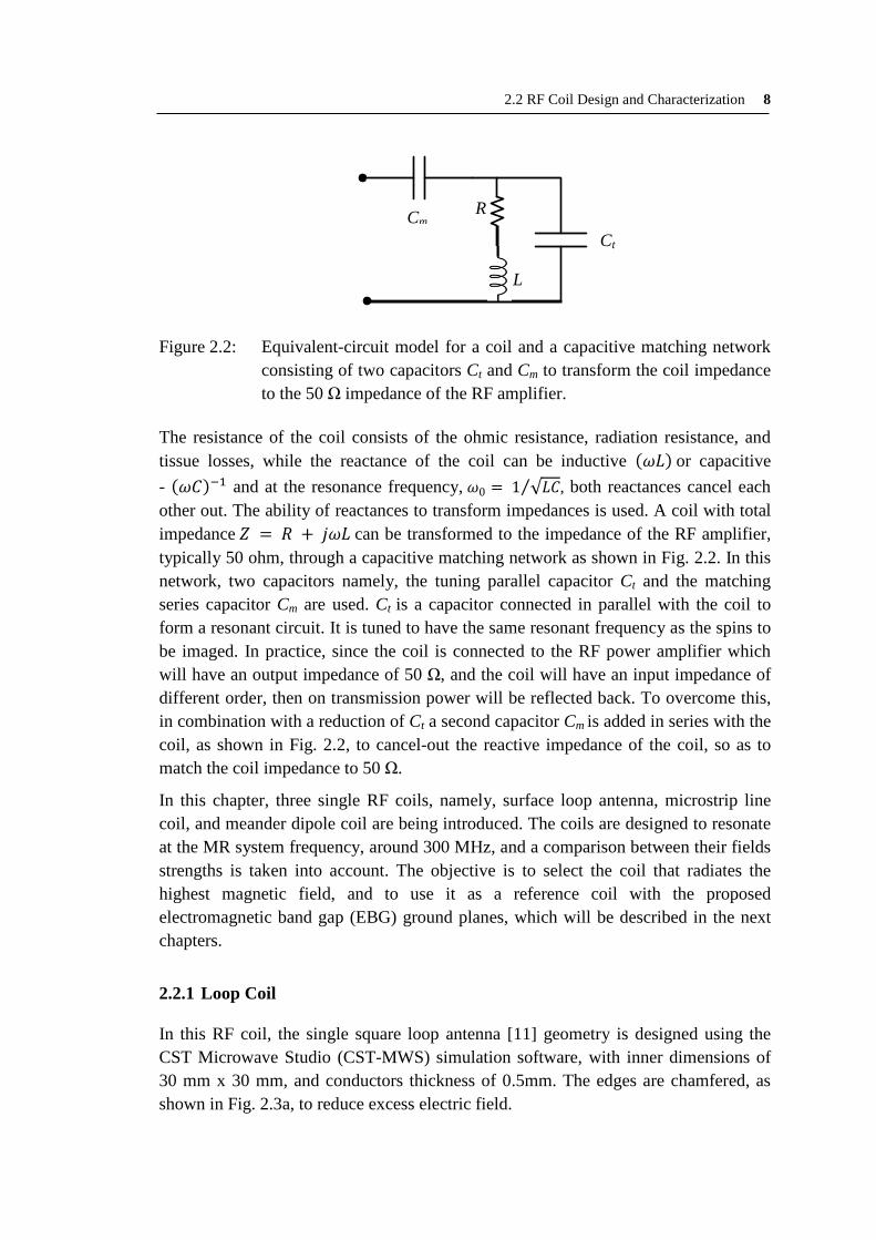
2.2 Equivalent-circuit model for a coil and a capacitive matching network consisting of two capacitors Ct and Cm to transform the coil impedance to the 50 Ω impedance of the RF amplifier……………………………… 8
2.3 (a) Square loop RF coil element with four discrete ports (b) The loop coil in the presence of a homogeneous phantom mounted on a Plexiglas placed 2 cm above the coil………………………………………….......... 9
2.4 Matching and tuning network of a single loop coil element for 7 T MRI with a series capacitor Cm of 3.5 pF and a tuning parallel capacitor Ct of around 5.42 pF and 3 equal lumped capacitors C1 of values around 7.44 pF…………………………………………………………………… 9
2.5 Return loss (S1,1) of a coil tuned to a resonant frequency of 300 MHz….. 10 2.6
(a) Absolute magnetic field distribution 1cm above the coil (b) Absolute magnetic field distribution 1cm inside the phantom or 4 cm above the coil, (c) Absolute electric field distribution 1cm inside the phantom or 4cm above the coil. Peak field values are shown in the colored bar caption……........................................................................................... 11
2.7 (a) Longitudinal z-directed magnetic field distribution 1 cm inside the phantom, (b) Longitudinal electric field distribution 1 cm inside the phantom………………………………………………………………….. 11
2.8 A planer stripline element of quarter wavelength size…………………... 12 2.9 Perspective view of the MRI transmit element unit designed by CST and
showing the stripline coil printed over FR4 substrate and backed by a PEC ground plane at 20.7 mm from the coil, the Plexiglas and phantom are positioned 20 mm over the coil………………………………………. 12
2.10 Electrical schematic of the complete coil element …...………………….. 13 2.11 The modeling of the tuning and matching network in the CST-MWS co-
simulation: The end capacitors Cend adjusted to 3.28 pF, the parallel capacitors Ct = 11 pF and the series capacitor Cm = 2.2 pF………………. 13
ix
x List of Figures
2.12 Measured and simulated absolute magnetic field [A/m] versus the longitudinal axis of the stripline 1 cm above the bottom of the phantom. The measured result taken from Erwin L. Hahn institute for MRI [11]…. 14
2.13 Measured and simulated absolute electric field [V/m] versus the longitudinal axis of the stripline 1 cm above the bottom of the phantom. The measured data taken from Erwin L. Hahn institute for MRI [11]… 14
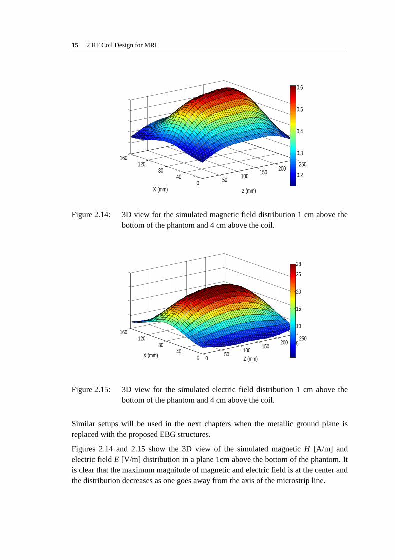
2.14 3D view for the simulated magnetic field distribution 1 cm above the bottom of the phantom and 4 cm above the coil…………………………. 15
2.15 3D view for the simulated electric field distribution 1cm above the bottom of the phantom and 4 cm above the coil…………………………. 15
2.16 Longitudinal field distribution 1 cm inside the phantom at various separation distances between the RF coil and the metallic ground plane (a) Magnetic field, (b) Electric field……………………………………... 16
2.17 Vertical field distribution from the center-bottom to the center-top inside the phantom, and at various separation distances of the phantom from the RF coil (a) Magnetic field, (b) Electric field………………………… 16
2.18 Meander dipole coil with linear dimension of quarter-wavelength……... 17 2.19 The practical realization of the tuning and matching network showing
the end capacitors Cend, the parallel capacitors Ct, and the series capacitor Cm……………………………………………………………… 18
2.20 Return loss (S1,1) with a resonant frequency 298 MHz at -23 dB, the series and parallel capacitors of the matching network are 2.87 pF and 9.4 pF respectively……………………………………………………….. 18
2.21 The simulated field distributions in a plane 1 cm above the bottom of the phantom and 4 cm above the meander dipole and stripline coils (a) Normalized magnetic field [A/m], and (b) Normalized electric field [V/m]. Fields are also normalized to the peak value…………………….. 19
3.1 A corrugated metal slab with one-quarter-wavelength slot height to exhibit very high impedance at the top surface………………………….. 21
3.2 A mushroom-like EBG structure and its composition…………………… 21 3.3 Wave amplitude of a wave bound to a high impedance surface and
decays into the surrounding space [16]….……………………………….. 23 3.4 (a) TM surface wave on a metallic surface, where electric field arcs out
of the surface, (b) TE surface wave on high impedance surface [16]…… 23 3.5
Radiation pattern of a monopole on (a) a metal ground plane, with ripples and wasted power, (b) A high-impedance ground plane, with smoother radiation pattern, and less wasted power in the backward hemisphere [16]…………………………………………………………..
24

List of Figures xi
3.6 (a) The unit cell brillouin zone, (b) The FEM simulation result for the dispersion diagram of the surface waves on the proposed mushroom-like EBG structure. Additional higher order bands are seen that are not predicted by the simple effective surface impedance model…………….. 26
3.7 (a) An antenna printed over a PEC ground plane with spacing << λ/4 causes a destructive interference, (b) An antenna printed over EBG ground plane with spacing << λ/4 has a constructive reflection effect…... 27
3.8 The numerical reflection coefficient phase of the proposed mushroom –like EBG structure, showing two useful frequency regions corresponding to the quadratic reflection phase 90o ± 45o and the in-phase reflection coefficient ±90o……………………………….............. 28
3.9 (a) Origin of the capacitance and inductance in the effective LC model and, Effective circuit used to model the surface impedance…………….. 30
3.10 Three-layer EBG structure………………………………………………. 30 3.11 The analytical result for the reflection coefficient phase of the proposed
mushroom-like EBG structure in Eq. (3.1) based on the effective medium model. The proposed structure has a sheet capacitance of 16.161 pF and a sheet inductance of 17.593 nH…………………………. 31
3.12 The predicted analytical dispersion diagram for surface waves on the proposed EBG structure. The surface supports the TM waves below the resonant frequency and TE waves at higher frequencies and near the resonance surface waves are suppressed of propagation………………… 32
3.13 High impedance surfaces. (a) Array of square metal plates with shorting vias. (b) Equivalent circuit of each resonator section [32]……………… 34
3.14 TE and TM plane wave incidences on a mushroom-like EBG structure… 35 3.15 Equivalent transmission line model for plane wave incidences [21]…… 35 3.16 The analytical reflection coefficient phase for TE-polarized plane waves
illuminate the proposed EBG structure at normal and oblique incidence.. 40 3.17 The analytical reflection coefficient phase for TM-polarized plane waves
illuminate the proposed EBG structure at normal and oblique incidence.. 40 3.18 The effect of the patch width W on the resonant frequency and
bandwidth of the proposed EBG structure……………………………….. 41 3.19 The effect of the gap width g on the resonant frequency and bandwidth
of the proposed EBG structure…………………………………………… 42 3.20 The effect of the substrate thickness h on the resonant frequency and
bandwidth of the proposed EBG structure……………………………… 43 3.21 The effect of the substrate permittivity εr on the resonant frequency and
bandwidth of the proposed EBG structure……………………………….. 43 3.22 A polarization-dependent PDEBG design with offset vias along the y-
axis (a) a single offset via, (b) double offset vias………………………...
44
xii List of Figures
3.23 Reflection phases of a PDEBG structure with a single offset via spaced at different distances from the edge of each patch under y-polarized incident wave…………………………………………………………….. 45
3.24 Reflection phases of a PDEBG structure with a pair of vias offset by a quarter of the patch width on each side under x and y- polarized incident wave……………………………………………………………………… 45
3.25 Dipole antenna over (a) EBG ground plane and (b) PEC or PMC ground plane……………………………………………………………………… 47
3.26 FDTD simulated return loss over a PEC, PMC, and EBG ground planes.. 48 3.27 Radiation pattern of a 0.41 λ300MHz dipole over the proposed EBG
structure, showing the θ and φ directed field on the yz plane with directivity around 10 dB…………………………………………………. 49
3.28 Radiation pattern of a 0.41 λ300MHz dipole over the proposed EBG structure at different radii………………………………………………... 49
3.29 (a) Return loss of a planar dipole antenna with a length varying from 0.44 λ300MHz to 0.38 λ300MHz, with useful operational frequency band (289-311) MHz. (b) Reflection phase of the proposed EBG structure with frequency region (283-308) MHz corresponding to the 90o ± 45o
reflection phase…………………………………………………………... 50 4.1 Stacked EBG design with unit cells of two layers of patches sharing the
same boundary…………………………………………………………… 53 4.2 Reflection phase characteristics of TE-polarized plane wave at oblique
incidence on the proposed stacked EBG structure: (a) with vias; (b) without vias………………………………………………………………. 55
4.3 Reflection phase characteristics of TM-polarized plane wave at oblique incidence on the proposed stacked EBG structure: (a) dual resonant behavior in the presence of vias (b) single resonant behavior in the absence of vias…………………………………………………………… 56
4.4 Dispersion diagram of the proposed EBG structure: (a) when vias of radius 1.73 mm are used; (b) In the absence of vias, where no surface wave band gap is exist…………………………………………………… 57
4.5 FDTD simulation result of the transmission (S2,1) scattering coefficient of the proposed stacked EBG structure…………………………………... 58
4.6 Offset layers stacked EBG design, with a lower layer of patches diagonally offset from the upper one. A meandered dipole sits 2 cm above the top surface of the proposed EBG structure…………………… 59
4.7 Reflection phase of the proposed offset and vertically stacked EBG structure based on the dimension in (4.2)………………………………... 61
4.8 Dispersion diagram of the proposed offset stacked EBG structure…….. 61 4.9 Experimental setup of the microstrip line test cell loaded by the finite
EBG structure……………………………………………………………. 62

List of Figures xiii
4.10 Measurement result and FDTD simulated transmission (S2,1) coefficient of the proposed offset stacked EBG structure……………..……………... 63
4.11 (a) EBG structure with vias diameter increased to 6 mm, (b) Measured transmission (S2,1) coefficient (dB)……………………….………………. 63
4.12 EBG structure with two layers of patches and vias……………………… 64 4.13 FDTD result of the transmission (S2,1) coefficient showing that the
existence of a second layer of vias reduces the overall inductance and shifts the resonance up in frequency………………………...…………… 64
4.14
FDTD simulation result of absolute magnetic field inside the phantom along the vertical direction, from the bottom-center to the top- center of the phantom. y = 0 is at the bottom of the phantom………………………
65
4.15 FDTD results of longitudinal normalized magnetic field at different heights inside the phantom (using EBG structure)……………………… 66
5.1
(a) Reflection coefficient phase of the reference EBG structure described in equation (5.1) with magneto-dielectric substrate of µr = 10.9 (b) Reflection coefficients phase of the reference EBG structure and the proposed miniaturized EBG structure with magneto-dielectric material (MDM)…………………………………………………………………… 70
5.2 The 1st, 2nd, and 3rd space filling curves (a) Hilbert curves, and (b) Peano curves………………………………………………………….. 71
5.3 x and y-polarized reflection coefficients phase of the first order Hilbert curve EBG structure……………………………………………………… 73
5.4 x and y-polarized resonant frequencies and bandwidths of EBG structures based on Hilbert curve inclusions of orders 1 to 3……………. 74
5.5 Normalized side dimension and bandwidth of EBG structure based on Hilbert curve inclusions of orders 1 to 3. Normalization is with respect to the MRI resonant wavelength λRES in the x-polarized direction, and with respect to the y-polarized resonant wavelength…………………….. 74
5.6 x and y-polarized wave incidence resonant frequency and bandwidth of EBG structures based on Peano curve inclusions of orders 1 and 2……... 76
5.7 Normalized side dimension and bandwidth of EBG structures based on Peano curve inclusions of orders 1 and 2. Normalization is with respect to the MRI resonant wavelength λRES in the x-polarized direction, and with respect to the y-polarized resonant wavelength…………………………… 76
5.8 The unit cell of the proposed EBG structure (a) Top view showing the Four-Leaf-Clover Shaped Patch (b) Side view…………………………...
78
5.9 Reflection phase of the proposed slotted and the reference solid patch... geometry offset stacked EBG structure with unit cell dimensions shown in (5.1)…………………………………………………………………….
79 5.10 Simulation model of direct transmission method………………………… 79

xiv List of Figures
5.11 S2,1 parameter of the proposed EBG structure inserted in a TEM waveguide with various cell numbers in a row…………………………... 80
5.12 Electric field distribution (a) at 300 MHz (inside the stop band gap), (b) at 200 MHz (outside the stop band gap), and (c) at 300 MHz in the absence of vias (no band gap)…………………………………………….. 81
5.13 Four-leaf clover-shaped offset stacked EBG design with a meandered dipole coil and a phantom………………………………………………… 81
5.14
FDTD longitudinal (z-axis) distribution of magnetic over electric field ratio for meander dipole coil backed by the proposed EBG structure and a metallic ground plane of the same size………..………………………...
82 5.15 Magnetic field Hx distribution in air at 1 cm above (a) 35 cm RF dipole
coil (b) 25 cm RF dipole coil. (FDTD simulation with EMPIRE)……….. 83 5.16 Geometry of the EBG structure with the proposed adjustable air-gap
with pins tuning method…………………………………………………. 85 5.17 The resonant frequency versus the air gap thickness……………………. 86 5.18 Coaxial cross-sections showing the inner conductor, the outer conductor,
and a dielectric…………………………………………………………… 87 5.19 EBG unit cell geometry with the proposed coaxial cable to tune the
resonant frequency by changing the vias lengths………………………... 87 5.20 Reflection coefficient phase of EBG structure with tuning coaxial cables
of different lengths……………………………………………………….. 89 5.21 Upper and lower resonant frequencies of four-leaf clover-shaped EBG
structure with coaxial cables of different lengths………………………... 89 6.1
An electromagnetic wave incident on a periodic ground plane. The incident angle 𝜃𝑖, longitudinal direction 𝑙, and transverse direction �̂� are labeled in the figure.................................................................................... 94
6.2 Realization of soft surface by metallic transversal corrugation grooves.... 97 6.3 Realization of hard surface by metallic longitudinal corrugation grooves. 97 6.4 Realization of soft and hard surfaces by a strip-loaded grounded
dielectric slab…………………………………………………………….. 98 6.5 The unit cell of the proposed gangbuster dipole FSS (a) Perspective
view, (b) Top view……………………………………………………….. 99 6.6 The reflection phase versus the incidence angle theta and at different
frequencies for a soft gangbuster dipole FSS…………………………… 100 6.7 The reflection phase versus the incidence angle theta and at different
frequencies for a hard gangbuster dipole FSS…………………………… 100 6.8 The unit cell of the proposed gangbuster slot FSS (a) Perspective view,
(b) Top view………………………………………………………………
101 6.9 The reflection phase of a hard slot-type gangbuster surface for oblique
incidence and with respect to different polarizations. Direction of propagation is along the slots…………………………………………….. 102

List of Figures xv
6.10 The reflection phase of a soft slot-type gangbuster surface for oblique incidence and with respect to different polarizations. Direction of propagation is orthogonal to the slots……………………………………. 102
6.11 (a) Meander dipole backed by a PEC, (b) Meander dipole backed by 4x3 cells of the proposed EBG ground plane. Later each row of transverse patches was connected together………………………………………….. 103
6.12 The proposed unit cell of the soft surface (a) Top view, (b) Side view….. 104 6.13 Reflection phase of the proposed soft surface with TM- and TE-
polarized plane wave at oblique incidence, and at different frequencies... 105 6.14 The fabricated soft surfaces (a) 12.8 cm x 25 cm, (b) 8.2 cm x 25 cm...... 106 6.15 Experimental setup of the microstrip line test cell loaded by a finite soft
surface......................................................................................................... 106 6.16 Simulated and measured transmission (S2,1) coefficient of the proposed
12.8 cm x 25 cm soft surface…………………………………………….. 107 6.17 Measured transmission (S2,1) coefficient of the two fabricated soft
surfaces…………………………………………………………………... 107 6.18 Normalized magnetic field strength |H| [A/m/√W] 4 cm inside the
phantom………………………………………………………………….. 108 6.19 Normalized electric field strength |E| [A/m/√W] 4 cm inside the
phantom………………………………………………………………….. 109 6.20 The ratio of |𝐻| �𝑆𝐴𝑅𝑚𝑎𝑥⁄ at 4 cm inside the phantom……………….... 109 6.21 The ratio of |H|/|E| at 4 cm inside the phantom…………………………. 110 7.1 (a) Offset layers stacked EBG design (b) Metallic PEC ground plane. A
dipole coil sits above the PEC and EBG ground planes in a height of 2 cm, and a homogeneous phantom sits above the coil in a height of 2 cm.............................................................................................................. 114
7.2 FDTD results of the maximum local 10g-based SAR and the whole body average SAR for 1 W accepted power by inside a phantom when the coil is backed by a PEC and an EBG ground planes………………………….. 114
7.3 Geometry of the complete simulation design, showing the meander dipole coil, two dielectric overlays, capacitors, FR4 supporting substrate, ground Plane, and a homogenious phantom above the coil……………… 116
7.4 (a) Magnetic field distribution at the bottom surface of a phantom, 2 cm above the coil. (b) Electric field distribution at the bottom surface of a phantom, 2 cm above the coil. Field values are normalized to �𝑃𝑎𝑐𝑐……. 117
7.5 (a) Magnetic field distribution in air, 1 cm above the coil (1 cm below the phantom), (b) Electric field distribution in air, 1 cm above the coil (1 cm below the phantom). Field values are normalized to �𝑃𝑎𝑐𝑐……………... 117
7.6 S1,1 parameters when substrates of various dielectric constants are used, and all with Cend = 0.5 pF………………………………………………… 118

xvi List of Figures
7.7 FDTD simulation of the longitudinal field distribution at the bottom surface of a phantom 2 cm above the coil for the cases of without and with overlays of different dielectric constants. (a) Normalized magnetic field [A/m/√W] (b) Normalized electric field [ V/m/√W]…………….. 119
7.8 Normalized peak-localized 10g-based SAR inside a phantom without and with dielectric substrates of different permittivities………………… 120
7.9 Dipole coil backed by the proposed soft surface to reduce the SAR…….. 121 7.10 The longitudinal total electric field strength 1 cm inside the phantom for
a meander dipole coil backed by (a) Perfect electric conductor PEC, and (b) The proposed soft surface–EBG ground plane. Field values are normalized to �𝑃𝑎𝑐𝑐……………………………………………………… 122
7.11 The 10g-based and 1g-based SAR 1 cm inside a homogeneous phantom sits 2 cm above a meander dipole coil backed by the proposed soft surface and a PEC ground plane of the same size. All SAR values have been normalized to an accepted power of 1W…………………………… 122

List of Abbreviations
AMC Artificial Magnetic Conductor DNG Double NeGative EBG Electromagnetic Band Gap FDTD Finite Difference Time Domain FEM Finite Element Method FID Free Induction Decay FOV Field Of View FSS Frequency Selective Surface HIS High Impedance Surface LH Left Handed MEMS Micro-Electro-Mechanical System MRI Magnetic Resonance Imaging NMR Nuclear Magnetic Resonance NRI Negative Refractive Index PBC Periodic Boundary Condition PBG Photonic Band Gap PCB Printed Circuit Board PDEBG Polarization-Dependent Electromagnetic Band Gap PEC Perfect Electric Conductor PMC Perfect Magnetic Conductor RF Radio Frequency SAR Specific Absorption Rate SNR Signal to Noise Ratio TE Transverse Electric TM Transverse Magnetic TEM Transverse ElectroMagnetic
xvii

Chapter 1
Introduction and Overview
Objectives of the Thesis Transmit RF coils for ultrahigh field MRI based on loop or stripline concepts are usually placed above a conducting ground plane. These metallic reflectors create anti-phase currents which cancel the radiation from the original coil current, and support surface waves which radiate at the edges and interfere destructively with coil space waves. Thus, the RF magnetic flux density above the coil (inside the load) is reduced.
The aim of this thesis is to investigate possible improvements of the performance of a well-established RF coil by replacing the conventional metallic ground plane with a high impedance surface - electromagnetic bandgap HIS-EBG structures. The proposed artificial ground plane is designed so that it reflects electromagnetic waves with no phase reversal, and the currents on its surface appear in-phase. Furthermore, surface waves on the top surface of the EBG structure are suppressed.
This thesis proposes the first application of EBG structures as ground planes for RF coils, in particular those operating at around 300 MHz for 7 Tesla MRI. The unique band gap features of the proposed EBG structures are investigated analytically, numerically, and validated by measurements.
The condition for a successful application of the EBG structure in MRI application is unique in that the cell dimensions are required to be far below the size of the RF coil, which in our case is 25% of the free-space wavelength. To reach this goal, different miniaturized techniques are studied and analyzed.
Structure of the Thesis The second chapter of this thesis reviews the concepts and principles of Magnetic Resonance Imaging (MRI) and Radio Frequency (RF) coils. Different RF coils are presented and their near fields inside a phantom positioned above them are investigated. The objective in this chapter is to select the best coil that provides the highest magnetic flux density B1 and to use it with the proposed EBG structures in next chapters in order to further improve their performance.
1

2 1 Introduction and Overview
In chapter 3, different circuit models are introduced to characterize and design EBG structures, including the effective medium model with lumped LC elements, and the transmission line model for surface wave and plane wave characterization. Analytical and numerical results are generated to describe the electromagnetic properties of EBG structures, namely, the in-phase reflection coefficient feature which leads to artificial magnetic conductor (AMC), and the stop band gap feature which describes the surface wave suppression. A parametric study of a mushroom-like EBG structure is presented, and the use of EBG structures for low profile wire antenna applications is investigated as an example of an advantageous application of EBG structures.
In chapter 4, multilayer stacked EBG structures are analyzed and proposed as ground planes for MRI RF coils. The reflection coefficient phase at normal and oblique incidence is studied, and the dispersion diagram is used to determine the TE and TM surface wave suppression band gap. In this chapter, the first application of an EBG structure to improve the B1 efficiency of RF coils used for 7-Tesla MRI is introduced. The magnetic field inside a homogeneous phantom over a meander dipole RF coil when it is backed by a PEC or stacked EBG ground planes are investigated and compared.
In chapter 5, different techniques are presented for the miniaturization of EBG structures. These include the high permeability Magneto-Dielectric sheets, the space filling curves which depend on the compactness of the EBG surface, and the polarization-dependent PDEBG structures. A four-leaf clover-shaped EBG structure based on elongating the path through which the currents pass is proposed to resonate at the MRI operating frequency with smaller unit cell dimensions. The magnetic over electric field ratio of a dipole RF coil backed by the PEC and the proposed EBG ground planes are compared, and the field of view (FOV) is investigated. In this chapter, some tuning techniques are introduced for the purpose of adjusting the band gaps of EBG structures. These include an adjustable air-gap layer with vias connected to the bottom surface of the EBG structure, and coaxial cables connected to the vias.
In chapter 6, some anisotropic surface impedance, namely, the soft and hard surfaces are introduced and their surface impedances and reflection coefficients are studied and compared to those of a perfect electric conductor (PEC) and perfect magnetic conductor (PMC). A novel multilayer offset stacked polarization dependent EBG structure is designed with considerably reduced dimensions and fabricated to work as a soft surface. The stop band gap property of the proposed soft surface is numerically investigated and validated by measurements. The magnetic and electric field strengths inside the phantom of the RF coil when it is backed by the soft ground plane are investigated and compared to the case when it is backed by a PEC ground plane of the same size.

3 1 Introduction and Overview
In chapter 7, the specific energy absorption rate (SAR) values inside the phantom are investigated and compared for the case when the meandered dipole RF coil is backed by a PEC and when it is backed by EBG ground planes. Two promising techniques are introduced to reduce the SAR values in the load. These include dielectric overlays mounted on the folded parts of the well-established dipole RF coil, and the novel soft surface-EBG structure which has been presented in the previous chapter.
In Chapter 8, the most important conclusions of this thesis are summarized and some proposals are presented for future works.

Chapter 2
RF Coil Design for MRI
In this chapter, an introduction to the concepts and principles of Magnetic Resonance Imaging (MRI) and Radio Frequency (RF) coils is given. Different single elements RF coils that could be used for surface or volume MRI coils will be discussed and investigated. The objective here is to compare the near fields inside phantoms positioned at different distances from various RF coils without or with reflectors at different heights from the coils. These characterisations provide the ability to select the best coil, which provides the highest magnetic field. In the rest of the thesis, the selected RF coil will be used with the proposed high impedance surface - electromagnetic band gap (HIS-EBG) structures to maximize the strength of the magnetic field in order to further improve the imaging capabilities of MRI.
2.1 Principles of Magnetic Resonance Imaging (MRI) Spins and Magnetizations Since its first implementation by Lauterbur [1], Magnetic Resonance Imaging (MRI) has become a non-invasive imaging technique that provides excellent soft tissue contrast with high resolution and no ionizing radiation. MRI is based on the phenomenon of Nuclear Magnetic Resonance (NMR), independently discovered by Bloch et al. [2] and Purcell et al. [3]. The NMR phenomenon is observed when a macroscopic sample of atomic nuclei in a static magnetic field is irradiated by an oscillating magnetic field of frequency ω that equals the frequency of precession, ω0
[4]. Atomic nuclei are composites of protons and neutrons which themselves composites of fundamental particles possess a quantum mechanical property called spin. For simplicity one can think of protons and neutrons as spheres that rotate around their axes. Only nuclei with an odd number of protons and neutrons have a resulting spin. The spinning nuclei possess angular momentum, L, and charge and the motion of this charge gives rise to an associated magnetic moment, μ, such that [5]:
𝜇 = 𝛾𝐿�⃗
(2.1)
where γ is the gyromagnetic ratio [MHz/Tesla] and depends on the nucleus. Hydrogen is the most prevalent element in the human body, because it is an elementary part of water and fat. The hydrogen nucleus 1H has more importance in MRI because it
4

5 2 RF Coil Design for MRI
possesses the least complex nucleus, a single positively charged proton, and of all the elements gives the strongest magnetic resonance signal. For 1H the γ/2π has a value of 42.58 MHz/Tesla.
In field-free space, the total of all proton spins in a volume element are randomly oriented and their effects cancel each other, resulting in no effective moment. In the presence of static magnetic field B0, spin up and spin down are the two preferred spin orientations, parallel and anti-parallel to the magnetic field lines (parallel to z-axis), resulting in a small majority of excess spins magnets precessed around B0 with a magnetization effect 𝑀��⃗ . The frequency of this precession is called the Larmor frequency 𝜔0 = 𝛾 𝐵0, and the spin precession is a kind of movement similar to that of the spinning tops, where the spin moves in the shape of a cone in the direction of B0 [6], as shown in Fig. 2.1. These up and down spin orientations are corresponding to two states of energy E+ and E-. The down spin has higher energy (E+), antiparallel state, than in the absence of B0 (E), and the up spin has lower energy (E-), parallel state, and the latter is preferred as more spins jump into the lower energy state than into the higher one. The ratio of parallel states to anti parallel states can be explained by Boltzmann distribution
kThB
eNN π
γ2
0
=+
−
(2.2)
where kT is the Boltzmann energy with k being the Boltzmann constant, k = 1.38 ∙ 10-23 WsK-1, h is Planck’s constant, h = 6.626 ∙ 10-34 Js, and B0 is the absolute value of the external magnetic flux density 𝐵�⃗ 0. This means, there are excess spins aligned parallel to the static magnetic field 𝐵�⃗ 0 resulting in a weak but measurable longitudinal equilibrium magnetization effect 𝑀��⃗ 0 which can be described for 1H with a given proton density ρ as:
kTBhM
40
22
0
ργ
= (2.3)
Spin Excitation and Relaxation The longitudinal magnetization (z-axis) can be deflected from its state of equilibrium by applying an external, transverse RF field B1 with a rotational frequency that meets the resonance condition (i.e. the oscillating frequency of the RF pulse has to match the Larmor frequency of the spins). Thus, the magnetization vector is rotated from the z-axis toward the xy-plane by an angle α, called the flip angle, as shown in Fig. 2.1. The stronger the energy of the exciting RF pulse, the farther the magnetization will flip or tilt. If a so-called “90° pulse” is applied, the magnetization vector will be rotated into the transverse x-y plane.

2.1 Principles of Magnetic Resonance Imaging (MRI) 6
Figure 2.1: Spin precession and magnetization (a) Spin rotates around its axis and
wobbles in the shape of a cone about B0, (b) Longitudinal and transverse components of a magnetization vector M tilted due to B1 field by an angle α, called flip angle.
The notation of the B1-field is commonly split up into a portion that rotates clockwise along with the precession of the magnetic moment of the spin system ( +
1B ) and a
portion that rotates anti-clockwise ( −1B ) [7]
2
,1,11
yx iBBB
+=+ ;
( )2
*,1,1
1yx iBB
B−
=−
(2.4)
Here B1,x and B1,y are the x and y complex components of the vector 𝐵�⃗ 1 of the local RF field. 𝐵1+ is referred to as the local transmit RF field, and 𝐵1− is referred to as the local received RF field.
After the start of the externally applied excitation pulse has been transmitted, magnetization vector precesses around B0 with ω0, and acts like a rotating magnet. During the precession, the transverse magnetization relaxes because of nuclear interactions and nonuniformity of B0 [4]. From Faraday's law of induction it follows that the time-varying magnetization induces a voltage in a coil. This measurable voltage is the received MR signal, called free induction decay (FID), which decays exponentially over time due to relaxation. The stronger the applied B1 field, the stronger the transverse magnetization, and hence the stronger the MR signal.
The spin relaxation is the process which restores the thermal equilibrium of the magnetic moment M0 (magnetization vector lies again in the direction of B0), and it is determined by two time constants T1 and T2. In the Bloch model [2], T1 is the spin-lattice relaxation time which describes the recovery of the longitudinal magnetization Mz (parallel to B0) to its equilibrium state due to thermal perturbations. It indicates how quickly a spin ensemble in a certain type of tissue will be able to emit its excess energy to the environment [6]. According to [2], T2 is the spin-spin relaxation time, which describes the decay of the transverse Mxy component of the magnetization vector due to internuclear interactions. The spin-spin interaction describes the loss of
(a) (b)
Z
MMz
Mxy
α
B0
M
ω

7 2 RF Coil Design for MRI
phase coherence of spins as they interact with each other via their own oscillating magnetic fields. As a result, the precession of spins moves out of phase and the overall transverse magnetization is reduced [8]. After a 900 RF pulse and time constant T1, the longitudinal magnetization Mz recovers to approximately 63% of its final value, and after T2, the transversal magnetization Mxy decays to about 37%. Fortunately, the relaxation time is not the same everywhere, it is tissue-dependent, and this contributes to high levels of image contrast which enable one to clearly depict pathological tissues.
For a more in-depth description of spin dynamics and quantum mechanics, the reader is referred to standard textbooks [9-10].
2.2 RF Coil Design and Characterization The radio frequency (RF) system consists of transmitter and receiver. The RF transmitter (Tx) generates a magnetic field B1 that rotates the magnetization of the spin away from the axis of the main static field B0 at an angle α, called flip angle, determined by the strength and pulse duration τ of the B1 field [8]. Thus, the transmitter path of the MR system delivers amplitude and phase-controlled RF pulses to one or more RF antennas, known by the MRI community as RF coils. Each RF coil broadcasts the RF signal to the patient and/or receives the return signal.
In the receive system (Rx), the signal of the excited spin is picked up. An effective means to improve signal to noise ratio (SNR), without lengthening scan time, is selecting an appropriate RF coil to pick up the signals. At 7T MRI and due to technical limitations, each local coil include RF transmit and receive features [8].
When a current I flows through an RF coil, spatially dependent magnetic field ( )rB 1
is being generated, and can be represented by the law of Biot-Savart as follows:
Here ld
is an infinitesimal element of the conductor and r is the displacement vector pointing from the conductor element to the point where the magnetic field is being computed, and 0µ [NA-2] is the magnetic permeability constant in vacuum.
For maximum power transfer from the RF amplifier to the conductors of the RF coil, through coaxial cables, impedance matching is essential so that at the resonant frequency the conjugate impedance of the amplifier matches the transformed impedance of the coil. The total impedance of a coil Z combines a real quantity R, and a complex part, the reactance X.
( ) ∫×
= 30
1 4 rrldIrB
πµ
(2.5)
2.2 RF Coil Design and Characterization 8
Figure 2.2: Equivalent-circuit model for a coil and a capacitive matching network
consisting of two capacitors Ct and Cm to transform the coil impedance to the 50 Ω impedance of the RF amplifier.
The resistance of the coil consists of the ohmic resistance, radiation resistance, and tissue losses, while the reactance of the coil can be inductive (𝜔𝐿) or capacitive - (𝜔𝐶)−1 and at the resonance frequency, 𝜔0 = 1 √𝐿𝐶⁄ , both reactances cancel each other out. The ability of reactances to transform impedances is used. A coil with total impedance 𝑍 = 𝑅 + 𝑗𝜔𝐿 can be transformed to the impedance of the RF amplifier, typically 50 ohm, through a capacitive matching network as shown in Fig. 2.2. In this network, two capacitors namely, the tuning parallel capacitor Ct and the matching series capacitor Cm are used. Ct is a capacitor connected in parallel with the coil to form a resonant circuit. It is tuned to have the same resonant frequency as the spins to be imaged. In practice, since the coil is connected to the RF power amplifier which will have an output impedance of 50 Ω, and the coil will have an input impedance of different order, then on transmission power will be reflected back. To overcome this, in combination with a reduction of Ct a second capacitor Cm is added in series with the coil, as shown in Fig. 2.2, to cancel-out the reactive impedance of the coil, so as to match the coil impedance to 50 Ω.
In this chapter, three single RF coils, namely, surface loop antenna, microstrip line coil, and meander dipole coil are being introduced. The coils are designed to resonate at the MR system frequency, around 300 MHz, and a comparison between their fields strengths is taken into account. The objective is to select the coil that radiates the highest magnetic field, and to use it as a reference coil with the proposed electromagnetic band gap (EBG) ground planes, which will be described in the next chapters.
2.2.1 Loop Coil In this RF coil, the single square loop antenna [11] geometry is designed using the CST Microwave Studio (CST-MWS) simulation software, with inner dimensions of 30 mm x 30 mm, and conductors thickness of 0.5mm. The edges are chamfered, as shown in Fig. 2.3a, to reduce excess electric field.
R
Cp
Cs
L
Cm Ct
R

9 2 RF Coil Design for MRI
Figure 2.3: (a) Square loop RF coil element with four discrete ports (b) The loop
coil in the presence of a homogeneous phantom mounted on a Plexiglas placed 2 cm above the coil.
Figure 2.4: Matching and tuning network of a single loop coil element for 7T MRI
with a series capacitor Cm of 3.5 pF and a tuning parallel capacitor Ct of around 5.42 pF and 3 equal lumped capacitors C1 of values around 7.44 pF.
The loop has four gaps of 5 mm, which are used for four discrete S-parameter ports; three of them would be replaced in the CST co-simulation with lumped elements to tune the coil to 300 MHz (7Tesla), or any other MR operating frequency. A homogenous phantom of size 310 mm by 160 mm and 90 mm thick is used to model a tissue liquid phantom of permittivity εr = 45.3 and conductivity σ = 0.87 S/m and mounted on 10 mm thickness Plexiglas of permittivity 2.6 and conductivity of 0.006 [S/m] placed 20 mm above the coil as shown in Fig. 2.3b. Three of the discrete S-parameter ports are modelled with lumped capacitors of equal values C1 to extend the coil length and tune the resonant frequency to the MR system frequency.
Port 1
C1
C1
C1
Ct
Cm
Square loop coil
Plexiglas Phantom
(a) (b) Coil
z
y
x
60mm
5mm
5mm
70m
m

2.2 RF Coil Design and Characterization 10
Figure 2.5: Return loss (S1,1) of a coil tuned to a resonant frequency of 300 MHz.
These capacitor values are fixed around 7.44 pF for 300 MHz (7 Tesla). For optimum transformation of RF power from the amplifier through coaxial cables, a tuning and matching network is used as shown in Fig. 2.4, with a tuning parallel capacitor Ct = 5.42 pF and a matching series capacitor Cm = 3.5 pF to match the loop to the impedance of the amplifier, 50 Ω. As seen from Fig. 2.5, the S1,1 parameter corresponding to the aforementioned capacitors in the tuning and matching network exhibits very good return loss minimum of -27 dB, indicating that the impedance of the coil is matched well to that of the amplifier.
The longitudinal (z-axis) absolute magnetic field distribution 1 cm above the loop element or 1 cm below Plexiglas is shown in Figure 2.6a. The effects of the tissue conductivity and permittivity on the magnetic and electric field distribution 1 cm inside the phantom (or 4 cm above the coil) are shown in Fig. 2.6b and 2.6c respectively. Only the values in the captions of Fig. 2.6 are peak values, while the whole other Figures and measurements in the rest of this thesis are rms values. All fields’ values are normalized to the square root of the accepted power,�𝑃𝑎𝑐𝑐.
Fig. 2.7a shows that the maximum magnetic field is found at the centre and then decreasing sharply along the edges of the phantom, thus more scanning time will be required when such a coil is used, and to maximize the field of view (FOV) an array of surface loop coils should be used.
It is observed from Fig. 2.7b that the minimum electric field is obtained at the centre of the phantom and the maximum values obtained at a position in the phantom corresponding to the distance between the centre of the coil and its arms.
100 200 300 400 500-30
-25
-20
-15
-10
-5
0
Frequency (MHz)
S11 p
ara
mete
r (d
B)

11 2 RF Coil Design for MRI
Figure 2.6: (a) Absolute magnetic field distribution 1 cm above the coil (b) Absolute magnetic field distribution 1 cm inside the phantom or 4 cm above the coil, (c) Absolute electric field distribution 1 cm inside the phantom or 4 cm above the coil. Peak field values are shown in the colored bar caption.
Figure 2.7: (a) Longitudinal z-directed magnetic field distribution 1 cm inside the
phantom, (b) Longitudinal electric field distribution 1 cm inside the phantom.
2.2.2 The Microstrip line (MSL) Coil In this section, a MSL coil of quarter-wavelength (λ300MHz/4) size is used as shown in Fig. 2.8. The coil is supported by FR4 dielectric substrate of permittivity ɛr = 4.3, and conductivity σ = 0.0205 [S/m], and of 100 mm x 250 mm size and backed by a perfect electric conductor (PEC) ground plane, as shown in Fig. 2.9 [11].
(a) (b) (c)
0 77.5 155 232.5 3100
0.2
0.4
0.6
0.8
1
1.2
Longitudinal distance (mm)
Mag
netic
fiel
d (A
/m)
0 77.5 155 232.5 310
5
10
15
20
25
30
35
Longitudinal distance (mm)
Ele
ctric
fiel
d (V
/m)
(a
(b)

2.2 RF Coil Design and Characterization 12
Figure 2.8: A microstrip line element of a quarter wavelength size.
Figure 2.9: Perspective view of the MRI transmit element unit designed by CST and showing the microstrip line coil printed over FR4 substrate and backed by a PEC ground plane at 20.7 mm from the coil, the Plexiglas and phantom are positioned 20 mm over the coil.
The separation between the coil conductors and the ground plane is fixed to 20.7 mm, and the thickness of the small piece connecting the upper and lower side of the element and carrying an end capacitor is 1 mm, as shown in Fig. 2.9. The metallic ground plane is fixed to a size of 100 mm x 250 mm. A tissue liquid phantom of 45.3 permittivity and 0.87 [S/m] conductivity and size of 310 mm x 160 mm x 90 mm is modeled in the simulation and mounted on 10 mm thickness Plexiglas of permittivity 2.6 and conductivity of 0.006 [S/m] as shown in Fig. 2.9. A two port technique was used in the simulation to model the feeding network in order to obtain more accurate results for the field calculations inside the phantom. The feeding is connected to the dipole strips by two wires of 0.6 mm diameter and 20.7 mm length.
The electrical schematic of the complete coil element including the tuning and matching capacitors as well as its modeling in the CST – MWS simulator are shown in Fig. 2.10 and Fig. 2.11 respectively. Two equal end capacitors Cend = 3.3 pF connect the quarter-wavelength MSL coil to the ground plane and extend its length to half-wavelength, Thus, the resonance is shifted down to the system frequency for 7T MRI, around 300 MHz. The matching network consists of a series and two identical parallel capacitors Cm = 2.55 pF and Ct = 10.95 pF respectively. A coaxial cable is connected to the coil as shown in Fig. 2.11, and its specifications are recorded in Table 2.1. Within the specified parameters, an excellent matching is obtained, and the coil resonates at 298 MHz with very good return loss of -30 dB.
15mm
250 mm
20.7mm
20mm
Plexiglas Phantom
Capacitor

13 2 RF Coil Design for MRI
Cend CendCp Cp
Cs
Figure 2.10: Electrical schematic of the complete coil element [11].
Figure 2.11: The modeling of the tuning and matching network in the CST-MWS
co-simulation: The end capacitors Cend adjusted to 3.28 pF, the parallel capacitors Ct = 11 pF, and the series capacitor Cm = 2.2 pF.
Table 2.1: Characteristics of the transmission line in the matching network.
Transmission line
Length 330 mm
Relative permittivity 2.3
Relative permeability 1
Impedance 50 Ω
Attenuation 0.478 dB/m
Port 1
Cend Cend
Coaxial Cable
Cm
Ct
Ct
≈ λ/2
MSL coil

2.2 RF Coil Design and Characterization 14
Figure 2.12: Measured and simulated absolute magnetic field [A/m] versus the longitudinal axis of the microstrip line 1 cm above the bottom of the phantom. The measured result taken from Erwin L. Hahn institute for MRI [11].
Figure 2.13: Measured and simulated absolute electric field [V/m] versus the longitudinal axis of the microstrip line 1 cm above the bottom of the phantom. The measured data taken from Erwin L. Hahn institute for MRI [11].
Figures 2.12 and 2.13 show the measured and simulated results for absolute magnetic field H [A/m] and absolute electric field E [V/m] values 1 cm inside the phantom or 4 cm over the MSL coil. The results exhibit very good correspondence between the simulated and measured results. Accordingly, this result is used as a reference with the other coils to investigate the best coil that provides the highest magnetic field.
0 77.5 155 232.5 3100
0.1
0.2
0.3
0.4
0.5
0.6
0.7
Longitudinal distance, Z (mm)
Mag
netic
fiel
d (A
/m)
MeasurementSimulation
0 77.5 155 232.5 310
5
10
15
20
25
30
35
Longitudinal distance, Z (mm)
Elec
tric
field
(V/m
)
MeasurementSimulation
15 2 RF Coil Design for MRI
Figure 2.14: 3D view for the simulated magnetic field distribution 1 cm above the bottom of the phantom and 4 cm above the coil.
Figure 2.15: 3D view for the simulated electric field distribution 1 cm above the
bottom of the phantom and 4 cm above the coil. Similar setups will be used in the next chapters when the metallic ground plane is replaced with the proposed EBG structures.
Figures 2.14 and 2.15 show the 3D view of the simulated magnetic H [A/m] and electric field E [V/m] distribution in a plane 1cm above the bottom of the phantom. It is clear that the maximum magnitude of magnetic and electric field is at the center and the distribution decreases as one goes away from the axis of the microstrip line.
50 100 150 200250
040
80120
160
z (mm)X (mm)
0.2
0.3
0.4
0.5
0.6
050
100150
200250
040
80120
160
Z (mm)X (mm)
5
10
15
20
25
28

2.2 RF Coil Design and Characterization 16
2.2.2.1 Ground Plane and Phantom Positions Effects
In this part, the effect of changing the position of the ground plane and the phantom with respect to the coil is investigated. First, the position of the ground plane is changed from 20.7 mm to 40.7 mm in steps of 10 mm, while the other parameters of the structure geometry are maintained, including a separation distance of 20 mm between the phantom and the coil. Fig. 2.16 shows that the magnetic and electric fields reduce with the increase in the separation distance between the coil and the ground plane, because less electromagnetic field will be reflected by the metallic ground plane.
Figure 2.16: Longitudinal field distribution 1 cm inside the phantom at various
separation distances between the RF coil and the metallic ground plane (a) Magnetic field, (b) Electric field.
Figure 2.17: Vertical field distribution from the center-bottom to the center-top inside the phantom, and at various separation distances of the phantom from the RF coil (a) Magnetic field, (b) Electric field.
0 77.5 155 232.5 3100
0.1
0.2
0.3
0.4
0.5
0.6
0.7
Longitudinal distance (mm)
Mag
netic
fie
ld (
A/m
)
h=20.7h=30.7h=40.7
0 77.5 155 232.5 310
5
10
15
20
25
30
Longitudinal distance (mm)
Ele
ctric
fiel
d (V
/m)
h=20.7h=30.7h=40.7
(a) (b)
0 15 30 45 60 75 900.1
0.2
0.3
0.4
0.5
0.6
0.7
0.8
0.9
Vertical distance, Y (mm)
Mag
netic
fiel
d (A
/m)
20mm 30mm 40mm 50mm
0 15 30 45 60 75 900
10
20
30
40
Vertical distance, Y (mm)
Ele
ctric
fiel
d (V
/m)
20mm 30mm 30mm 40mm
(a) (b)

17 2 RF Coil Design for MRI
Similarly, when the distance between the phantom and the coil is increased from 20 mm to 50 mm in steps of 10 mm, it is observed from Fig. 2.17 that the vertical magnetic and electric field distribution from the centre-bottom to the centre-top of the phantom is also reduced. The further the phantom from the coil the weaker the absorbed electromagnetic energy and hence the less is the magnetic field. This will affect the contrast and quality of images.
Because of the standing wave effects at the top surface of the phantom, in the simulation environment, the difference between the magnetic and electric fields distribution at different distances between the coil and the phantom decreases at the top surface of the phantom.
2.2.3 Meander Dipole Coil The resonant meandered dipole antenna proposed in [12, 13], and as shown in Fig. 2.18, is used at the Erwin L. Hahn Institute as RF coil for 7 Tesla MRI to maximize the magnetic field and reduce the coupling for multichannel RF coils. The coil is approximately half-wavelength dipole with more than half of the length of each arm folded in a meander to reduce the total length to λ300MHz/4, and to resonate at 298 MHz. It is printed on FR4 epoxy substrate of 0.5 mm thickness and elevated above a 100 mm wide reflector plate. The entire height between the dipole and the PEC ground plane as well as the separation distance between the coil and the phantom, and the whole configuration are kept similar to that of the microstrip line coil described in section 2.2.2. To compare in a fair manner between the performance of this coil and the MSL coil, a phantom of the same dimensions and properties was utilized.
6 mm
250 mm
Figure 2.18: Meander dipole coil with linear dimension of a quarter-wavelength.
The magnitude of the magnetic and electric field strength inside the phantom when the meander dipole is used was investigated and compared with the results obtained in the case when the previous MSL coil element is used.
15mm 65mm

2.2 RF Coil Design and Characterization 18
Figure 2.19: The practical realization of the tuning and matching network showing the end capacitors Cend, the parallel capacitors Ct, and the series capacitor Cm.
Figure 2.20: Return loss (S1,1) with a resonant frequency 298 MHz at -23 dB, the series and parallel capacitors of the matching network are 2.87 pF and 9.4 pF respectively.
Two capacitors Cend connect the end arms of the meander dipole coil and the ground plane to form a loop, and are adjusted to 2 pF to shift the resonance down to the MR system frequency 298 MHz. The matching network for this coil element is modelled in the CST co-simulation as in Fig. 2.11, and its practical realization is shown in Fig. 2.19. The network consists of two capacitors connected in parallel with the coil Ct each of 9.4 pF, and a series capacitor Cm of 2.87 pF to match the impedance of the coil to the amplifier impedance, typically 50 Ω.
100 200 300 400 500-25
-20
-15
-10
-5
0
Frequency (MHz)
S11 p
ara
mete
r (d
B)
19 2 RF Coil Design for MRI
Figure 2.21: The simulated field distributions in a plane 1 cm above the bottom of
the phantom and 4 cm above the meander dipole and MSL coils (a) Normalized magnetic field [A/m], and (b) Normalized electric field [V/m]. Fields are also normalized to the peak value.
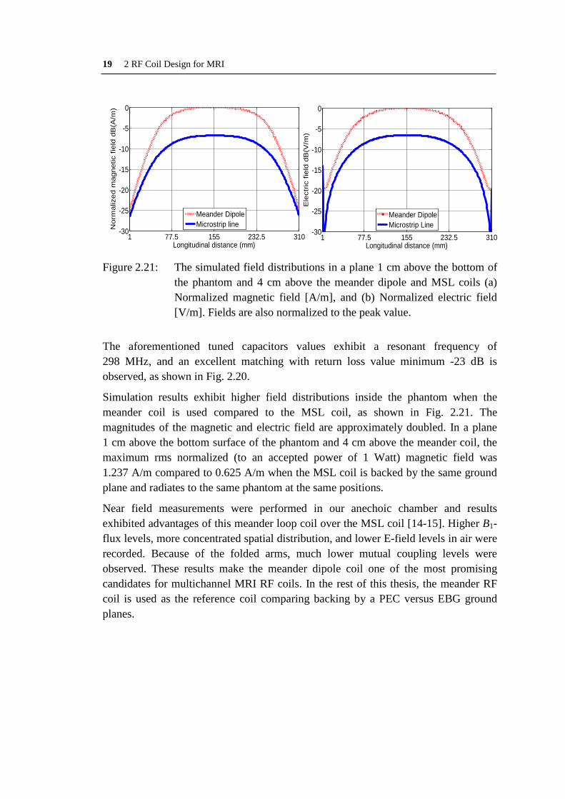
The aforementioned tuned capacitors values exhibit a resonant frequency of 298 MHz, and an excellent matching with return loss value minimum -23 dB is observed, as shown in Fig. 2.20.
Simulation results exhibit higher field distributions inside the phantom when the meander coil is used compared to the MSL coil, as shown in Fig. 2.21. The magnitudes of the magnetic and electric field are approximately doubled. In a plane 1 cm above the bottom surface of the phantom and 4 cm above the meander coil, the maximum rms normalized (to an accepted power of 1 Watt) magnetic field was 1.237 A/m compared to 0.625 A/m when the MSL coil is backed by the same ground plane and radiates to the same phantom at the same positions.
Near field measurements were performed in our anechoic chamber and results exhibited advantages of this meander loop coil over the MSL coil [14-15]. Higher B1- flux levels, more concentrated spatial distribution, and lower E-field levels in air were recorded. Because of the folded arms, much lower mutual coupling levels were observed. These results make the meander dipole coil one of the most promising candidates for multichannel MRI RF coils. In the rest of this thesis, the meander RF coil is used as the reference coil comparing backing by a PEC versus EBG ground planes.
1 77.5 155 232.5 310-30
-25
-20
-15
-10
-5
0
Longitudinal distance (mm)
Ele
ctric
fie
ld d
B(V
/m)
Meander DipoleMicrostrip Line
1 77.5 155 232.5 310-30
-25
-20
-15
-10
-5
0
Longitudinal distance (mm)
Nor
mal
ized
mag
netic
fie
ld d
B(A
/m)
Meander DipoleMicrostrip line
Chapter 3
Characterization of EBG Structures
This chapter focuses on the characterization and design of EBG structures based on various resonant circuit models. The effective medium model with lumped LC elements is introduced, and the transmission line model for surface waves as well as plane waves is also explained. The useful surface wave suppression band gap and the frequency region where the structure reflects the field in-phase are extracted analytically and numerically from the dispersion diagram and the reflection coefficient properties respectively. A parametric study of the proposed mushroom-like EBG structure is presented. A polarization-dependent EBG (PDEBG) structure based on offsetting the vias position is studied. The advantage of high impedance surfaces for low profile wire antenna is described and its utilization to improve the radiation efficiency is investigated.
3.1 Introduction to EBG Structures The term “metamaterial” is used to describe composite materials with unique features and useful properties. Metamaterials are periodic material composites of metals and dielectrics and possess properties from the structures rather than compositions [16].
According to the electromagnetic properties of metamaterial, different terminologies are introduced in the literature, such as: double negative (DNG) materials, left-handed (LH) materials, negative refractive index (NRI) materials, magneto dielectric material, Soft and hard surfaces, high impedance surface (HIS), and artificial magnetic conductor (AMC). In the literature, also various terminologies are used based on the domain of the applications. These include filter design, frequency selective surfaces (FSS) [17], photonic crystals [18] and photonic band gaps (PBG) [19], etc. They are classified under the broad terminology of “Electromagnetic Band Gap (EBG)” structures [20]. In general, EBG structures are artificial periodic objects that prevent or assist the propagation of electromagnetic waves in a specified band of frequency [21].
EBG structures are broadly classified as metamaterial due to their unique band gap features and high impedance properties. They exhibit interesting properties, like the reflection coefficient phase, and the surface wave suppression band gap property.
20
21 3 Characterization of EBG Structures
Y
Z
λ/4
<< λ/4
X
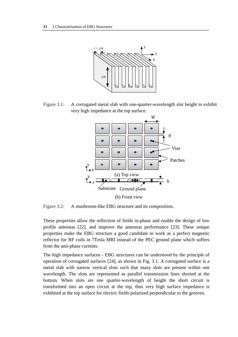
Figure 3.1: A corrugated metal slab with one-quarter-wavelength slot height to exhibit
very high impedance at the top surface.
Figure 3.2: A mushroom-like EBG structure and its composition.
These properties allow the reflection of fields in-phase and enable the design of low profile antennas [22], and improve the antennas performance [23]. These unique properties make the EBG structure a good candidate to work as a perfect magnetic reflector for RF coils in 7Tesla MRI instead of the PEC ground plane which suffers from the anti-phase currents.
The high impedance surfaces - EBG structures can be understood by the principle of operation of corrugated surfaces [24], as shown in Fig. 3.1. A corrugated surface is a metal slab with narrow vertical slots such that many slots are present within one wavelength. The slots are represented as parallel transmission lines shorted at the bottom. When slots are one quarter-wavelength of height the short circuit is transformed into an open circuit at the top, thus very high surface impedance is exhibited at the top surface for electric fields polarized perpendicular to the grooves.
Patches
W
g
h
(a) Top view
(b) Front view
y
z x
z
ɛr r
Ground plane Substrate
Vias

3.1 Introduction to EBG Structures 22
The high-impedance surfaces presented by Sievenpiper [16] can be considered as a kind of two-dimensional (2-D) textured surfaces that can be used to alter the electromagnetic properties of metal surfaces with much less than one-quarter-wavelength thick, to perform a variety of functions. They are typically built as subwavelength mushroom-shaped metal protrusions on a flat metal sheet connected to a metal backed dielectric substrate by vertical metal-plated vias, as shown in Fig 3.2. These surfaces provide a high-impedance boundary condition for both polarizations and for all propagation directions [25]. They reflect the fields with no phase reversal, rather than out-of phase as with an electric conductor. In addition to their unusual reflection-phase properties, they do not support surface waves, as with an electric conductor. These surfaces may be considered as a kind of electromagnetic bandgap (EBG) structure [25].
In this chapter, a mushroom like EBG structure is designed to resonate around the MRI operating frequency. The proposed structure will be introduced to describe the unique electromagnetic properties of high impedance surfaces analytically (based on different circuit models) and numerically. The HFSS full wave simulator from Ansoft, based on FEM algorithm was used to design and characterize one unit cell of the EBG structure surrounded by periodic boundary conditions (PBCs) to model an infinite EBG structure.
The proposed EBG structure is designed with the electrical dimensions shown in (3.1) to exhibit very high impedance at the top surface, so that the MRI operating frequency is located inside its useful reflection and surface wave suppression band gaps. Such structure is composed of four parts: a periodic metal patch printed on the top of a grounded dielectric slab, and vertical vias connecting the two metal sheets, as shown in Fig. 3.2.
W = 0.097 λ300MHz, g = 0.001 λ300MHz, h = 0.014 λ300MHz, 𝜀𝑟 = 10.2, and r = 0.004 λ300MHz.
(3.1)
Here, λ300MHz is the free space wavelength at 300 MHz (roughly the operating frequency for 7Tesla MRI) which is used as a reference length, W is the patch width, g is the gap width, and h is the thickness of the dielectric substrate with relative permittivity ɛr.
The main useful electromagnetic properties of EBG structures are the reflection coefficient phase and the suppression of surface waves.
3.1.1 Surface Waves The properties of surface waves can be derived by solving for waves that are bound to a surface and decay exponentially away from a surface with impedance Zs and decay constant α [16], as shown in Fig. 3.3.

23 3 Characterization of EBG Structures
Figure 3.3: Wave amplitude of a wave bound to a high impedance surface and
decays into the surrounding space [16]. For TM waves, the surface impedance is given as follows:
(3.2)
For TE waves, the surface impedance is given by the expression:
(3.3)
Here, ω is the angular frequency of the wave, ɛ and µ are the permittivity and permeability of the space surrounding the surface. From (3.2) and (3.3) it is clear that TM waves occur on a surface with positive reactance, i.e. inductive surface impedance, and TE waves occur on a capacitive surface.
For TM waves propagating on a metal sheet, the magnetic field is transverse to the surface, and the electric field arcs out of the surface, as shown in Fig. 3.4a. TE surface waves on a high impedance surface have dual form as shown in Fig. 3.4b.
Figure 3.4: (a) TM surface wave on a metallic surface, where electric field arcs out of the surface, (b) TE surface wave on high impedance surface [16].
(a)
(b)

3.1 Introduction to EBG Structures 24
Figure 3.5: Radiation pattern of a monopole on (a) a metal ground plane, with ripples and wasted power, (b) A high-impedance ground plane, with smoother radiation pattern, and less wasted power in the backward hemisphere. [16].
One property of lossy metals is that they support surface waves. These waves propagate and are bound to the interface between the metal and free space and radiate when scattered by bends or discontinuities.
When a monopole antenna is placed near to a metallic reflector, as shown in Fig. 3.5a, the antenna will radiate plane waves into free space and generate currents propagating on the metal sheet in anti-phase to the antenna current. These currents radiate when they reach the edges and couple to the external plane waves [25], and cause a multipath interference seen as ripples in the forward direction of the antenna radiation pattern, and cause wasted power in the backward direction.
Near the resonant frequency region of the high impedance surface, each row of metal patches has opposite charge, and the surface waves propagating along the EBG surface will be inhibited and form the standing waves, which results in the surface waves suppression band gap. Thus, a smoother radiation pattern with less wasted power in the backward hemisphere is observed, as shown in Fig. 3.5b.
(a)
(a)
(b)
(b)

25 3 Characterization of EBG Structures
The dispersion diagram which describes the stop bandgap through which surface waves are suppressed from propagation and the reflection phase property and its different useful band gaps can be obtained numerically as described below.
Dispersion Diagram For an accurate representation of the surface wave property, some commercial numerical electromagnetic full wave simulators are used, like the HFSS from ANSYS, and the CST Microwave Studio. The simulators discretize the structure on a grid and solve numerically the equations which describe the EM fields at all points on the grid. In this part, the HFSS full wave simulator based on the finite element method (FEM) algorithm is used to design and characterize EBG structures by simulating one unit cell surrounded with four periodic boundary conditions (PBCs) [26] to model an infinite EBG structure. The dispersion relation between the wavenumber k and the frequency ω is plotted out and referred to as the dispersion diagram.
For a periodic structure, such as the EBG surface, the field distribution of a surface wave is also periodic [27] with a phase delay determined by the wavenumber k and periodicity a, and expressed as follows:
( ) ( ) nxjkxezyxEzynaxE −=+ ,,,,
(3.4)
Here, n is an arbitrary integer number. The periodicity and the propagation direction of the waves are assumed in the x direction with a wavenumber kx. Each surface wave mode can be decomposed into an infinite series of space harmonic waves, as described below [21]
( ) ( )∑∞
−∞=
−=n
xjkn xnezyEzyxE ,,, ,
( ) ( )
ankk xxn
πωω 2+=
(3.5)
In (3.5), the dispersion relation kx (ω) is periodic along the x axis with a periodicity of 2π/a. Thus, the dispersion relation can be plotted within one single period, namely 0 ≤ kxn ≤ 2π/a, which is known as the Brillouin zone [28]. For two-dimensional periodic structures, the Brillouin zone becomes a two-dimensional square area, and can be represented as follows:
,20x
xn ak π
≤≤
,20y
yn ak π
≤≤ (3.6)
When the proposed high impedance surface described in (3.1) is used, the dispersion diagram is plotted as shown in Fig. 3.6b. The vertical axis represents the frequency and the horizontal axis represents the transverse wavenumbers values (kx, ky). Three specific points are:
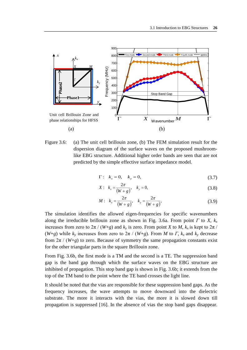
3.1 Introduction to EBG Structures 26
Figure 3.6:
(a) The unit cell brillouin zone, (b) The FEM simulation result for the dispersion diagram of the surface waves on the proposed mushroom-like EBG structure. Additional higher order bands are seen that are not predicted by the simple effective surface impedance model.
,0,0: ==Γ yx kk
(3.7)
( ) ,0,2: =
+= yx k
gWkX π (3.8)
( ) ( ) ,
2,2:gW
kgW
kM yx +=
+=
ππ (3.9)
The simulation identifies the allowed eigen-frequencies for specific wavenumbers along the irreducible brillouin zone as shown in Fig. 3.6a. From point Γ to X, kx increases from zero to 2π / (W+g) and ky is zero. From point X to M, kx is kept to 2π / (W+g) while ky increases from zero to 2π / (W+g). From M to Γ, kx and ky decrease from 2π / (W+g) to zero. Because of symmetry the same propagation constants exist for the other triangular parts in the square Brillouin zone.
From Fig. 3.6b, the first mode is a TM and the second is a TE. The suppression band gap is the band gap through which the surface waves on the EBG structure are inhibited of propagation. This stop band gap is shown in Fig. 3.6b; it extends from the top of the TM band to the point where the TE band crosses the light line.
It should be noted that the vias are responsible for these suppression band gaps. As the frequency increases, the wave attempts to move downward into the dielectric substrate. The more it interacts with the vias, the more it is slowed down till propagation is suppressed [16]. In the absence of vias the stop band gaps disappear.
y
x
Unit cell Brillouin Zone and phase relationships for HFSS
Γ
X M
Phase1
Phas
e2
(b) (a)
kx
ky
0
100
200
300
400
500
600
700
800
900
Freq
uenc
y (M
Hz)
Wavenumber
First mode Second mode Third mode Fourth mode lightline
Stop Band Gap
ΓΓ MX

27 3 Characterization of EBG Structures
3.1.2 Reflection Phase
In addition to the surface wave suppression property, high impedance surfaces (HISs) exhibit an unusual reflection phase property. In this interesting property, the image currents of an antenna on the EBG surface have the same direction as the antenna currents. This is achieved when the operating frequency of the antenna is located inside the useful frequency region corresponding to the in-phase reflection coefficient of the EBG structure.
Fig. 3.7a shows an antenna printed over a flat metal sheet reflector. For a short distance between the radiating element and the metallic reflector, the antenna will appear short circuited to the ground plane and the radiation is reduced. This is caused by the destructive effect of the image currents on the metallic ground plane which has opposite direction to the currents in the antenna. A quarter-wavelength distance between the antenna and the ground plane is required to avoid the poor radiation efficiency, but this is not suitable for limited space applications. The EBG structure, as shown in Fig. 3.7b, is introduced as an artificial ground plane solution with an image current in-phase rather than out of phase with the antenna current. Thus, a constructive effect is realized and the problem above can be solved without the quarter-wavelength space. The reflection phase property of EBG structures can be used to maximize the reflected field above the surface, or to provide good return loss with very close proximity between the antenna and the artificial ground plane.
Figure 3.7: (a) An antenna printed over a PEC ground plane with spacing << λ/4 causes a destructive interference, (b) An antenna printed over EBG ground plane with spacing << λ/4 has a constructive reflection effect.
PECWave 1
Wave 2
Antenna
4/λ<<
destructive interference
Wave 1
Wave 2
Antenna
4/λ<<
Constructive superposition
(a) (b)

3.2 Circuit Models of EBG Ground Planes 28
Figure 3.8: The numerical reflection coefficient phase of the proposed mushroom-like EBG structure, showing two useful frequency regions corresponding to the quadratic reflection phase 90o ± 45o and the in-phase reflection coefficient ±90o.
EBG structures exhibit a frequency dependent reflection coefficient phase varying between +180o to −180o compared to 180o for the perfect electric conductor (PEC) and 0° for the perfect magnetic conductor (PMC), which is not available in nature.
The reflection coefficient curve of the EBG structure based on the dimension described in (3.1) is shown in Fig. 3.8. There are two useful frequency regions corresponding to this reflection coefficient phase. The first frequency region is corresponding to the quadratic -phase reflection coefficient (90o ± 45o ), where the structure can be used to provide good return loss for low profile wire antenna applications [21]. The second frequency region is corresponding to the in-phase reflection coefficient (+90oto −90o ), where the EBG structure radiates in-phase rather than out of phase as in the PEC case and it has zero degree at the resonant frequency. Near the zero degree reflection phase, the tangential magnetic field is near to zero and the EBG structure exhibits very high surface impedance, and behaves like an artificial magnetic conductor (AMC).
3.2 Resonant Circuit Models for EBG Ground Planes The operation mechanism and the unique features of EBG structures in this section can be analyzed by some circuit models, namely, lumped elements model, and periodic transmission line models, whiles more complicated frequency selective surfaces (FSS) can be characterized only by full wave numerical methods.
100 150 200 250 300 350 400 450 500-200
-150
-100
-50
0
50
100
150
200
Frequency [MHz]
Ref
lect
ion
phas
e [d
eg]

29 3 Characterization of EBG Structures
The mushroom-like EBG structure with the electrical dimensions in (3.1) is analytically characterized with different circuit models. These models include the effective medium model with lumped LC elements and the transmission line model for surface waves and plane waves. The analytical analysis for the predicted reflection phase and some features of the suppression band gaps of surface waves on the EBG surface in the context of the effective surface impedance models will be explained in this section.
3.2.1 Effective Medium Model with Lumped LC Elements The use of the effective medium model with equivalent lumped LC elements to describe an EBG structure is valid as long as the periodicity (W+g) is much smaller than the operating wavelength [16]. This model is used for surface wave and plane wave reflection. For the square lattice mushroom-like EBG structure shown in Fig. 3.9, the capacitor comes from the gap between the adjacent patches and its value C is given by the fringing capacitance between neighboring coplanar metal plates. The conducting paths through the vias and the ground plane provide a sheet inductance L [25]. The behavior of the EBG structure can be reduced to a parallel resonant circuit as shown in Fig. 3.9b. The structure can be modeled analytically by using the simple parallel LC resonant circuit. The impedance of this circuit is the surface impedance Zs
and is given by:
LCLjZs 21 ω
ω−
= (3.10)
with sheet capacitance C and sheet inductance L. The resonance frequency of the circuit is calculated as follows:
LC1
0 =ω
(3.11)
At low frequencies the surface is inductive and supports TM waves, and at high frequencies the surface becomes capacitive and supports TE waves, and near the resonance frequency ω0 the surface impedance (Zs) is much greater than the free space impedance. Near the resonant frequency region, TM waves form the standing waves in which each row of metal patches has opposite charge. TE waves are not bound to the surface; instead, they radiate readily into the surrounding space as leaky waves [29]. Therefore, there are no surface waves flowing along the EBG structure in this frequency region, and the surface-wave suppression bandgap established.
The value of the capacitance C can be found using conformal mapping, a technique for determining two-dimensional electrostatic field distributions [16].

3.2 Circuit Models of EBG Ground Planes 30
W g
h2r
ɛr
Figure 3.9: (a) Origin of the capacitance and inductance in the effective LC model
and, (b) Effective circuit used to model the surface impedance
The solution starts from a pair of plates surrounded by 𝜀𝑟1 from one side (usually air) and 𝜀𝑟2 on the other and the edge capacitance between the two plates is given as follows:
( )
++= −
ggWCosh
WC rr 1210
πεεε (3.12)
For lower frequency applications, three layers EBG structures can be used, as shown in Fig. 3.10. This design is used to achieve a lower resonant frequency for a given thickness by capacitive loading [25]. The capacitance here is given by the well-known formula for a parallel plate capacitor. A is the overlap area of the plates, ε is the dielectric constant of the insulating material, and d is the distance between the plates.
dAC ε
= (3.13)
CapacitorLayer 1
Layer 2
Figure 3.10: Three-layer EBG structure.
The sheet capacitance is determined by the product of the individual capacitors and a geometric factor F that depends on the choice of lattice. For a square lattice F = 1, for a triangular lattice 𝐹 = √3, and for a hexagonal grid of capacitors 𝐹 = 1 √3⁄ [25]. For more complicated geometries, a full wave simulator should be applied.
In the effective medium model, a solenoid of current is used to model the current path in the high impedance surface, and to calculate its sheet inductance L [30]. The magnetic field through the solenoid is calculated by ampere’s law, and the inductor value is determined from the energy stored in its magnetic field.
L
C C
L
(a) (b)
Zs

31 3 Characterization of EBG Structures
Figure 3.11: The analytical result for the reflection coefficient phase of the proposed mushroom-like EBG structure in Eq. (3.1) based on the effective medium model. The proposed structure has a sheet capacitance of 16.161 pF and a sheet inductance of 17.593 nH.
The inductance L depends on the substrate thickness h of the EBG structure and the permeability µ = µ0 µr, and can be expressed as follows:
𝐿 = 𝜇 ℎ (3.14)
This effective surface impedance model summarizes the properties of EBG surfaces into a single parameter, the surface impedance Zs.
Once the surface impedance Zs is known, the reflection coefficient phase for the effective medium model can be represented as follows:
ηη
+−
=Γs
s
ZZ
(3.15)
Here, η represents the plane wave impedance in free space. Figure 3.11 shows the analytical result for the reflection coefficient phase of the mushroom-like EBG structure described by the electrical dimensions in (3.1). At very low frequencies, the reflection phase is π and the EBG structure behaves like a metal, at the resonance frequency the reflection phase crosses zero and the EBG structure behaves like a magnetic conductor, and at higher frequencies above the resonance the phase returns to −𝜋. When the surface impedance is greater than the impedance of free space the phase falls within π/2 and −𝜋/2. The shadow area in Fig. 3.11 represents the frequency range corresponding to this in-phase reflection coeffiecient. From the effective medium model, the dispersion relation is also calculated and some features of the surface wave suppression band gaps are determined.
100 200 300 400 500-180
-135
-90
45
0
45
90
135
180
Frequency (MHz)
Ref
lect
ion
phas
e (d
egre
es)
In-Phase
Out-of-Phase
Out-of-Phase
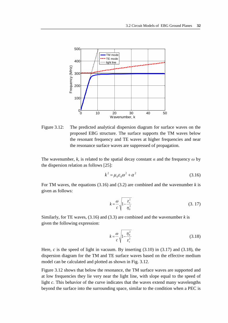
3.2 Circuit Models of EBG Ground Planes 32
Figure 3.12: The predicted analytical dispersion diagram for surface waves on the proposed EBG structure. The surface supports the TM waves below the resonant frequency and TE waves at higher frequencies and near the resonance surface waves are suppressed of propagation.
The wavenumber, k, is related to the spatial decay constant α and the frequency ω by the dispersion relation as follows [25]:
2200
2 αωεµ +=k (3.16)
For TM waves, the equations (3.16) and (3.2) are combined and the wavenumber k is given as follows:
20
2
1η
ω szc
k −= (3. 17)
Similarly, for TE waves, (3.16) and (3.3) are combined and the wavenumber k is given the following expression:
2
201szc
kηω
−= (3.18)
Here, c is the speed of light in vacuum. By inserting (3.10) in (3.17) and (3.18), the dispersion diagram for the TM and TE surface waves based on the effective medium model can be calculated and plotted as shown in Fig. 3.12.
Figure 3.12 shows that below the resonance, the TM surface waves are supported and at low frequencies they lie very near the light line, with slope equal to the speed of light c. This behavior of the curve indicates that the waves extend many wavelengths beyond the surface into the surrounding space, similar to the condition when a PEC is
0 10 20 30 40 500
100
200
300
400
500
Wavenumber, k
Freq
uenc
y (M
Hz)
TM modeTE modelight line

33 3 Characterization of EBG Structures
used. Near the resonant frequency, the dispersion curve is bent over away from the light line indicating that the surface waves are tightly bound to the surface and have a very low group velocity. Above the resonant frequency, the surface is capacitive and TE waves are supported, and at high frequencies the curve bends away from the light line and the waves are more tightly bound to the surface [30].
This model predicts some features of the stop band gap and the reflection phase properties of EBG structures. The static field approximation of the effective medium model limits its accuracy, because the field interaction between cells is not taken in consideration [31]. Furthermore, the effect of the radius of the vias is not taken into account, and the model is only useful for normal plane wave incidence. Thus, more accurate models are required to be used, as the transmission line model.
3.2.2 Transmission Line Model for Surface Waves The theory of transmission line and periodic circuits are used to analyze and model surface waves that propagate in horizontal directions on the surface of 2-D EBG structures [32]. Figure 3.13a shows an EBG structure with square patches connected to the ground plane through vias. In this method, each of the reactively loaded resonators shown in Fig. 3.13a can be modeled by its equivalent circuit, as shown in Fig. 3.13b. The total impedance between two nodes of the periodic structure consists of the resonator impedance Zp and a capacitive reactance Xc represents the coupling capacitor between the adjacent resonators, with capacitance C represented as in (3.12).
The vias in Fig. 3.13a represent the inductive reactance Xl, with an inductance value equal to [32]:
𝐿 = 2 × 10⁻⁷ �In �4ℎ𝑑� + 0.5 �
𝑑ℎ� − 0.75�
(3.19)
where h and d are the length and diameter of the conductive vias respectively. From transmission-line theory, the impedance of each resonator can be expressed as follows [33]:
𝑍𝑝 = 𝑍𝑙 .
1 + 𝑗 𝑍0𝑍𝑙
tan(𝛽𝑢𝑙)
1 + 𝑗 𝑍𝑙𝑍0
tan(𝛽𝑢𝑙)
(3.20)
Here, Z0 is the characteristics impedance and βu is the phase constant of the unloaded transmission line, Zl is the loading impedance which transformed by a transmission line of length l into the impedance Zp at the input terminal. The transmission line is approximated by a microstrip line with the same line width and substrate properties as the mushroom-like EBG structure.

3.2 Circuit Models of EBG Ground Planes 34
Figure 3.13: High impedance surfaces. (a) Array of square metal plates with
shorting vias. (b) Equivalent circuit of each resonator section [32].
Once the resonator impedance Zp and the coupling capacitor Xc are known, the EBG structure in Fig. 3.13a can be represented as a transmission line periodically loaded with a lumped impedance Z consisting of the combination of Zp and Xc with a period a.
The phase constant β can be represented for an infinite lossless periodic structure with a periodicity a as follows [32]:
( ) ( ) ( )a
ZZjaa uu βββ sin
2coscos
0
+=
(3.22)
The dispersion diagram of the periodic structure can be obtained by calculating the propagation constant at different frequencies. This method is applicable to analyze the propagation and suppression of surface wave, and it is not used for plane wave incidences.
3.2.3 Transmission Line Model for Plane Waves In the effective medium model for the mushroom-like EBG structure proposed in [16], each unit cell is characterized by its quasistatic parameters, capacitance and
L
Zp
Z0, βu Z0, βu
W/2 W/2
Front view
Top view (a)
(b)
h d
g
W
a
C

35 3 Characterization of EBG Structures
inductance. Thus the strong field interconnection between the cells is not taken in consideration [31] and only roughly estimated from the parameters of individual cell. Another model for TM waves along the Sievenpiper structure was introduced in [34], and it is based on the TM modes analysis of Fakir's grounded bed-of-nails structure, which was presented in [35]. In [34] the distance between the patches and the ground plane was replaced by a transmission line filled by a dielectric, and the capacitive grids modeled by an equivalent capacitive reactance.
A more accurate method based on the transmission line model was presented in [36, 37]. In this model the mutual coupling between cells are taken into account and the model is valid for small unit cells compared to the wavelength (a ˂˂ λ) and narrow gap widths between the patches (g ˂˂ W).
This model is used to characterize the reflection phase of the EBG structure at normal and oblique plane wave incidence. The model is used for TM and TE polarization (see Fig. 3.14) in the presence and absence of vias.
In this loaded transmission line model, the EBG structure is decomposed into a frequency selective surface (FSS) with grid impedance Zg, and a metal backed dielectric slab with slab impedance Zd.
Figure 3.14: TE and TM plane wave incidences on a mushroom-like EBG structure.
Figure 3.15: Equivalent transmission line model for plane wave incidences [21].
Zs

3.2 Circuit Models of EBG Ground Planes 36
In the presence of vias, the spacing medium between the FSS and the metallic ground plane is treated as a wire medium. In this model, as shown in Fig. 3.15, the total surface impedance Zs is found as a parallel combination of Zg and Zd:
dg
dg
ZZZZ
Z+
=
(3.23)
and the resonant frequency at which the structure works as an artificial magnetic conductor has to satisfy:
( ) ( ) 000 =+ ωω dg XX (3.24)
where Xg and Xd are the imaginary parts of Zg and Zd respectively.
3.2.3.1 Grid Impedance of an FSS In this approach the capacitive grid impedance of arrays of square patches for oblique incidence is modeled by using the analytical models of the inductive grid impedance for strip arrays and the Babinet principle. For TE-incidence fields, the grid impedance for thin parallel conducting strips of width g is given as follows [31]:
αη
2effTE
g jZ =
(3.25)
and for TM-polarized fields
where ηeff is the wave impedance of the effective uniform host medium with relative effective permittivity ɛeff, and α is the grid parameter and it expresses the inductive susceptibility of the wire grid. The wave impedance of the effective medium can be defined as follows:
effeff
effε
ηεεµ
η 0
0
0 ==
(3.27)
where µ0, ɛ0, and η0 are the permeability, permittivity, and wave impedance in free space. The effective permittivity of the equivalent uniform medium can be approximated as [38]:
2
1+= r
eff
εε
(3.28)
The grid parameter α can be represented as [31]:
θαη 2cos
2effTM
g jZ =
(3.26)

37 3 Characterization of EBG Structures
=
waakeff
ππα
2log
(3.29)
Here, keff is the wave number of the incident wave vector in the effective uniform medium and expressed as a function of the wave number in free space k0 and the effective permittivity:
effeff kk ε0= (3.30)
The grid impedance for the complementary structure, i.e. for the patch arrays, for the TE-polarized fields is obtained by applying Babinet transformation for strip arrays in TM fields [31]
θα
ηη2cos24 jZ
Z eff
stripsg
effTEg ==
− (3.31)
Similarly, the grid impedance for the complementary structure for TM-polarized fields is obtained though Babinet principle and the grid impedance for the strip arrays in TE fields
α
ηj
Z effTMg 2
=
(3.32)
The strip width w in (3.29) should be replaced by the gap width g and grid parameter α expresses the capacitive susceptibility of the patch grid.
Therefore, the grid impedance Zg of an FSS depends on the polarization of the fields. Thus, for an array of square patches, the grid impedance at oblique incidence can be represented based on the above results for normal incidence (θ = 0) as [37]:
( ) ( )0,, ωθω gTMg ZZ = (3.33)
and the capacitive grid impedance at normal incidence is found as:
( )g
g CjZ
ωω 10, =
(3.34)
By equating (3.34) and (3.32) and by simple substitution of (3.27) and (3.29) a new formula for the grid capacitance is found as follows:
( )
+=
gaa
C rg ππ
εε 2log1 0
(3.35)
The grid impedance Zg of an FSS depends also on the shape of the patches, and for non-squared geometry another grid impedance equation can be obtained.
( ) ( ),
cos0,
, 2 θ
ωθω gTE
g
ZZ =
3.2 Circuit Models of EBG Ground Planes 38
3.2.3.2 Surface Impedance of a Metal-Backed Dielectric Slab For a metal backed dielectric substrate perforated by vias, the surface impedance of the slab Zd for TE-polarized fields is not affected by the presence or absence of the vias. The E-field is orthogonal to the vias, so the vias are not excited. Thus, the space between the patches and the ground plane can be considered as an isotropic medium slab, and the slab impedance at the top surface can be expressed as [31]:
( )hkjZ dz
r
TEd tan
sin 2
0
θε
η
−=
(3.36)
where 𝑘𝑑𝑧 = 𝜔�𝜇0𝜖0�𝜖𝑟 − 𝑠𝑖𝑛2𝜃 is the vertical component of the wave vector of the reflected wave. By simple mathematical manipulation and under the condition kdz
h << 1, the slab impedance in the presence or absence of vias for the TE-incidence plane wave can be represented as follows:
( )hj
khk
jZdz
dzTEd µωµω ≈=
tan
(3.37)
The surface impedance of the EBG structure is the parallel combination of Zg and Zd for the TE-polarized incidence:
θα
η2cos21 kh
jkhZ TE
s −=
(3.38)
The reflection coefficient as a function of incidence angle of the TE polarized plane wave can be computed as:
ηθηθ
+−
=Γcoscos
TEs
TEsTE
ZZ
(3.39)
For TM incident fields, the effect of vertical vias is taken into account and the slab impedance Zd can be considered as the impedance of a thin layer of a wire medium. It is shown in [31] that at low frequencies the surface impedance of the wire medium is simply the same as that of a TEM transmission line of length equal to the layer thickness, and can be represented as follows:
( )hkj
Z dr
TMd tan0
ε
η=
(3.40)
where the wave vector of the refracted wave 𝑘𝑑 = 𝜔�𝜇0𝜖0𝜖𝑟 and in the most interesting case kd h << 1, the slab impedance Zd for TM incidence fields is practically equal to that for TE incidence [39]:
hjZ TMd µω≈
(3.41)

39 3 Characterization of EBG Structures
For the TM polarization, the effect of the vias is seen in the fact that the slab surface impedance Zd does not depend on the incidence angle. The surface impedance of the whole EBG structure is the parallel combination of the slab impedance in (3.41) and the grid impedance in (3.33) and can be represented as follows:
αηhk
hjkZ TMs 21−
=
(3.42)
In the absence of the vias, the slab impedance Zd at TE incidence remains the same as in (3.41), while for the TM polarized fields it is strongly depends on the incident angle [39]:
θµω 2coshjZ TMd ≈
(3.43)
The corresponding surface impedance of the EBG structure for TM incidence and in the absence of the vias is computed by the parallel combination of (3.43) and (3.33) and expressed as:
θα
θη2
2
cos21cos
khjkhZ TM
s −=
(3.44)
The reflection coefficient is then computed as:
θηθη
coscos
+−
=Γ TMs
TMsTM
ZZ
(3.45)
The reflection phases for TE and TM polarized fields illuminating the surface at normal and oblique incidence can be analytically computed based on the aforementioned model and plotted for the proposed EBG structure as shown in Fig. 3.16 and Fig. 3.17 respectively. For the TE-polarized fields, the reflection coefficient phase depends on the incidence angle. The larger the angle of incidence the higher is the resonance frequency. For TM polarized incidences, the model exhibited less angle dependence for the reflection coefficient phase as shown in Fig. 3.17.
In this section, the analysis of the EBG structure properties based on the transmission line model and the Sievenpiper quasistatic model has been analytically investigated. It is found that the reflection phase obtained from these models coincide well with the numerical solution obtained from the FEM-full wave simulator HFSS (not shown here). For TE polarization at oblique incidence a slight shift is observed between the analytical and numerical results.
More description of the reflection coefficient phase property for oblique incidence in the presence and absence of vias are numerically described in chapter 4.
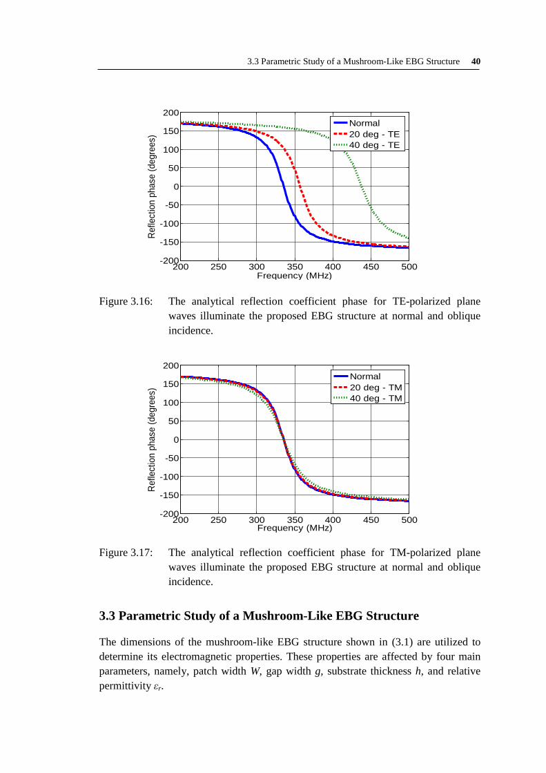
3.3 Parametric Study of a Mushroom-Like EBG Structure 40
Figure 3.16: The analytical reflection coefficient phase for TE-polarized plane waves illuminate the proposed EBG structure at normal and oblique incidence.
Figure 3.17: The analytical reflection coefficient phase for TM-polarized plane waves illuminate the proposed EBG structure at normal and oblique incidence.
3.3 Parametric Study of a Mushroom-Like EBG Structure The dimensions of the mushroom-like EBG structure shown in (3.1) are utilized to determine its electromagnetic properties. These properties are affected by four main parameters, namely, patch width W, gap width g, substrate thickness h, and relative permittivity εr.
200 250 300 350 400 450 500-200
-150
-100
-50
0
50
100
150
200
Frequency (MHz)
Refle
ctio
n ph
ase
(deg
rees
)
Normal20 deg - TE 40 deg - TE
200 250 300 350 400 450 500-200
-150
-100
-50
0
50
100
150
200
Frequency (MHz)
Refle
ctio
n ph
ase
(deg
rees
)
Normal20 deg - TM40 deg - TM

41 3 Characterization of EBG Structures
Figure 3.18: The effect of the patch width W on the resonant frequency and bandwidth of the proposed EBG structure.
In this section, plane waves illuminate the EBG surface at normal incidence, thus the vias are not exited and hence the radius of the vias has no effect. These four parameters and their effect on the EBG behavior are investigated.
The FEM full wave simulator HFSS is used to simulate one unit cell of the proposed EBG structure surrounded by periodic boundary conditions (PBCs) to model an infinite periodic structure. Within the variation of each of these four parameters, the resonant frequencies corresponding to 0o reflection phase and the bandwidths corresponding to ±90o reflection phase are recorded and plotted.
3.3.1 Square Patch Width Effect In this part, the role of the patch width in determining the resonant frequency and bandwidth of the proposed EBG structure is numerically analyzed. The width of the square patch is varied from 0.057 λ300MHz to 0.173 λ300MHz while the other parameters, namely the gap width, substrate thickness, and relative permittivity are kept constant.
Figure 3.18 shows the observed resonant frequencies (corresponding to 0o reflection phase) and bandwidths (corresponding to ±90o reflection phase) of the proposed EBG structure for different patch widths. It is clear from the Figure that increasing the patch width decreases the resonant frequency and bandwidth.
This behavior can also be analyzed from the lumped LC model. From (3.12) the increase in W increases the capacitance C which decreases the resonant frequency ω0
as in (3.11) and this ends up with steep reflection coefficient phase, and hence a narrow bandwidth.
57 77 97 117 137200
250
300
350
400
450
Patch Width [mm]
Reso
nant
Fre
quen
cy [M
Hz]
57 77 97 117 1375
7
9
11
13
15
Band
widt
h %
Res. FrequencyBandwidth

3.3 Parametric Study of a Mushroom-Like EBG Structure 42
Figure 3.19: The effect of the gap width g on the resonant frequency and bandwidth of the proposed EBG structure.
3.3.2 Gap Width Effect The gap width of each EBG unit cell determines the capacitive coupling effect with the other neighbor cells. Figure 3.19 shows the resonant frequency as well as the bandwidth as a function of the gap width of the proposed EBG structure. The gap width is changed from 0.0005 λ300MHz to 0.004 λ300MHz while the other parameters such as the patch width, substrate thickness, and the permittivity are kept constant as specified in (3.1). It is observed that the center frequency of the in-phase reflection coefficient and its corresponding bandwidth increases as the gap width between the patches of the EBG structure increases.
The gap width has an opposite effect to the patch width. In the lumped LC model, the increase in the gap width decreases the capacitance C. Thus, the resonant frequency increases and the slope of the reflection coefficient phase becomes flat, and the bandwidth is wider.
3.3.3 Substrate Thickness Effect The effect of changing the substrate thickness h on the resonant frequency and bandwidth of the EBG structure is investigated.
The height of the proposed EBG surface above the ground plane is changed from 0.006 λ300MHz to 0.022 λ300MHz while the other parameters are all maintained as in (3.1). As can be seen from Fig. 3.20, the increase in the height between the EBG surface and the ground plane has a positive effect in reducing the resonant frequency and increasing the bandwidth.
0.5 1 2 3 4260
280
300
320
340
360
Res
onan
t Fre
quen
cy [M
Hz]
Gap Width [mm]
0.5 1 2 3 48
8.5
9
9.5
10
10.5
Band
wid
th %
Res. FrequencyBandwidth

43 3 Characterization of EBG Structures
Figure 3.20: The effect of the substrate thickness h on the resonant frequency and
bandwidth of the proposed EBG structure.
Figure 3.21: The effect of the substrate permittivity εr on the resonant frequency and bandwidth of the proposed EBG structure.
It is noticed that the substrate thickness of the EBG structure has an opposite effect to the patch and gap widths parameters, because here the bandwidth changes in the opposite way to the resonant frequency.
This special property of the EBG structures can be described from the lumped LC model where the increase in h causes the inductance L to increase as in (3.14) while
6 10 14 18 22240
260
280
300
320
340
360
380
400
Res
onan
t Fre
quen
cy [M
Hz]
Substrate Thickness [mm]
6 10 14 18 224
5
6
7
8
9
10
11
12
Ban
dwid
th %
Res. FrequencyBandwidth
2 6 10.2 14 18200
300
400
500
600
700
800
Permitivity
Reso
nant
Fre
quen
cy [M
Hz]
2 6 10.2 14 185
10
15
20
Band
widt
h %
Res. FrequencyBandwidth

3.4 Polarization-Dependent EBG Structures 44
the capacitance remains unchanged. Thus, the frequency decreases, and the bandwidth increases.
3.3.4 Substrate Permittivity Effect The dielectric constant of the analyzed EBG structure is varied from 2 to 18 while the patch width, gap width, and substrate thickness are kept constant as in (3.1). It is found that the lower the relative permittivity of the EBG substrate the higher is the resonant frequency. It is observed that this increase in the resonant frequency is accompanied with more flat in-phase reflection coefficient. Thus, the bandwidth is also increased. The variation of resonant frequencies and bandwidths versus different dielectric constants is shown in Fig. 3.21.
3.4 Polarization-Dependent EBG Structures Polarization-dependent PDEBG structures can be realized from asymmetrical surfaces like the rectangular EBG surface, or by incorporating slots into the metallic patches of the EBG structure. These will be seen in some applications to MRI in the next chapters. In this section, a PDEBG structure is realized by offsetting the vias, as shown in Fig. 3.22.
The position of vias plays an important role in determining the resonance frequency. Figure 3.22 introduces an EBG design with the same dimensions as in (3.1). A single and double vias are offset at various distances from the edge of each patch.
Figure 3.22: A polarization-dependent PDEBG design with offset vias along the y-
axis (a) a single offset via, (b) double offset vias.
(a)Top view
(a) Front view
(b)Top view
(b) Front view y
z
x y
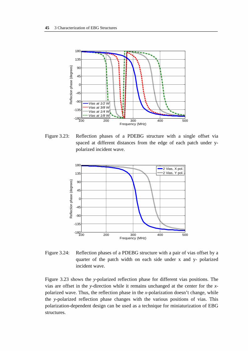
45 3 Characterization of EBG Structures
Figure 3.23: Reflection phases of a PDEBG structure with a single offset via spaced at different distances from the edge of each patch under y-polarized incident wave.
Figure 3.24: Reflection phases of a PDEBG structure with a pair of vias offset by a
quarter of the patch width on each side under x and y- polarized incident wave.
Figure 3.23 shows the y-polarized reflection phase for different vias positions. The vias are offset in the y-direction while it remains unchanged at the center for the x-polarized wave. Thus, the reflection phase in the x-polarization doesn’t change, while the y-polarized reflection phase changes with the various positions of vias. This polarization-dependent design can be used as a technique for miniaturization of EBG structures.
100 200 300 400 500-180
-135
-90
-45
0
45
90
135
180
Frequency (MHz)
Ref
lect
ion
phas
e (d
egre
es)
Vias at 1/2 WVias at 3/8 WVias at 1/4 WVias at 1/8 W
100 200 300 400 500-180
-135
-90
-45
0
45
90
135
180
Frequency (MHz)
Ref
lect
ion
phas
e (d
egre
es)
2 Vias, X pol.2 Vias, Y pol.

3.5 Low Profile Wire Antennas over EBG Ground Plane 46
As can be seen from Fig. 3.23, when the vias are at W / 2 from the edges of the patches (i.e at the center of patches) the x and y-polarized reflection phases are both represented by the solid curve. When the vias are shifted from the center of the patches a dual resonance behavior is observed in the y-polarized reflection coefficient phases. The closer the vias to the edge of the patches, the higher is the separation between the two frequencies. Whatever the shift in the vias position, the x-polarized reflection phases, which are not included in the figure, are all same as the solid line in Fig. 3.23, the case when the vias are at the center of the patches.
To investigate more deeply the resonance feature of the EBG structure, two symmetric vias are placed at equal distances (W / 4) from the patch boundaries, as shown in Fig. 3.22b. The x-polarized reflection phase remains again unchanged while the y-polarized reflection phase, as shown in Fig. 3.24, exhibits a resonance behavior similar to the higher resonance band in the case when one offset via at the same position is used. This means that the resonance feature depends on the distance of the vias from the patch edges. The lower resonance in the case of a single via seems to be an asymmetric mode which is cancelled in the symmetric via configuration.
3.5 Low Profile Wire Antennas over EBG ground plane One of the useful advantages of EBG structures is their ability to replace the conventional metallic ground plane in antenna applications where the overall height of the antenna structure is very small avoiding coupling effects with a nearby metallic ground plane.
In [40], it was observed that the operation frequency band where the EBG surface has a quadratic reflection phase in the range of (90o ± 45o ) is very close to the input-match frequency region. This region determines the frequency band where the EBG structure can be used for low profile wire antenna applications with efficient radiation patterns and good return loss.
In [41] an EBG structure at low frequency is introduced with a unit cell dimension of 140 mm and Teflon dielectric substrate of 40 mm thickness and 𝜀𝑟 = 2.2. In this section, a smaller EBG structure is presented for low profile wire antenna applications, and then compared with a perfect electric conductor (PEC) and perfect magnetic conductor (PMC) ground planes of the same size.
3.5.1 Comparison of PEC, PMC, and EBG Ground Planes The geometry of a planar dipole near a perfect electric conductor (PEC), perfect magnetic conductor (PMC), and electromagnetic band gap structure (EBG) ground planes is illustrated as shown in Fig. 3.25.
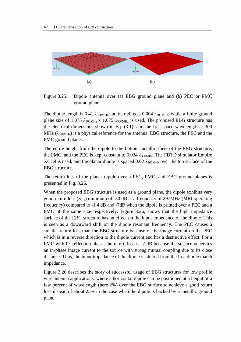
47 3 Characterization of EBG Structures
(a) (b)
Figure 3.25: Dipole antenna over (a) EBG ground plane and (b) PEC or PMC
ground plane. The dipole length is 0.41 λ300MHz and its radius is 0.004 λ300MHz, while a finite ground plane size of 1.075 λ300MHz x 1.075 λ300MHz is used. The proposed EBG structure has the electrical dimensions shown in Eq. (3.1), and the free space wavelength at 300 MHz (λ300MHz) is a physical reference for the antenna, EBG structure, the PEC and the PMC ground planes.
The entire height from the dipole to the bottom metallic sheet of the EBG structure, the PMC, and the PEC is kept constant to 0.034 λ300MHz. The FDTD simulator Empire XCcel is used, and the planar dipole is spaced 0.02 λ300MHz over the top surface of the EBG structure.
The return loss of the planar dipole over a PEC, PMC, and EBG ground planes is presented in Fig. 3.26.
When the proposed EBG structure is used as a ground plane, the dipole exhibits very good return loss (S1,1) minimum of -30 dB at a frequency of 297MHz (MRI operating frequency) compared to -1.4 dB and -7dB when the dipole is printed over a PEC and a PMC of the same size respectively. Figure 3.26, shows that the high impedance surface of the EBG structure has an effect on the input impedance of the dipole. This is seen as a downward shift on the dipole resonant frequency. The PEC causes a smaller return-loss than the EBG structure because of the image current on the PEC which is in a reverse direction to the dipole current and has a destructive effect. For a PMC with 0o reflection phase, the return loss is -7 dB because the surface generates an in-phase image current to the source with strong mutual coupling due to its close distance. Thus, the input impedance of the dipole is altered from the free dipole match impedance.
Figure 3.26 describes the story of successful usage of EBG structures for low profile wire antenna applications, where a horizontal dipole can be positioned at a height of a few percent of wavelength (here 2%) over the EBG surface to achieve a good return loss instead of about 25% in the case when the dipole is backed by a metallic ground plane.
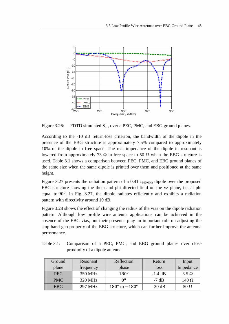
3.5 Low Profile Wire Antennas over EBG Ground Plane 48
Figure 3.26: FDTD simulated S1,1 over a PEC, PMC, and EBG ground planes.
According to the -10 dB return-loss criterion, the bandwidth of the dipole in the presence of the EBG structure is approximately 7.5% compared to approximately 10% of the dipole in free space. The real impedance of the dipole in resonant is lowered from approximately 73 Ω in free space to 50 Ω when the EBG structure is used. Table 3.1 shows a comparison between PEC, PMC, and EBG ground planes of the same size when the same dipole is printed over them and positioned at the same height.
Figure 3.27 presents the radiation pattern of a 0.41 λ300MHz dipole over the proposed EBG structure showing the theta and phi directed field on the yz plane, i.e. at phi equal to 90o. In Fig. 3.27, the dipole radiates efficiently and exhibits a radiation pattern with directivity around 10 dB.
Figure 3.28 shows the effect of changing the radius of the vias on the dipole radiation pattern. Although low profile wire antenna applications can be achieved in the absence of the EBG vias, but their presence play an important role on adjusting the stop band gap property of the EBG structure, which can further improve the antenna performance.
Ground plane
Resonant frequency
Reflection phase
Return loss
Input Impedance
PEC 350 MHz 180o -1.4 dB 3.5 Ω PMC 320 MHz 0o -7 dB 140 Ω EBG 297 MHz 180o to −180o -30 dB 50 Ω
250 275 300 325 350-45
-40
-35
-30
-25
-20
-15
-10
-5
0
5
Frequency (MHz)
Ret
urn
loss
(dB)
PECPMCEBG
Table 3.1: Comparison of a PEC, PMC, and EBG ground planes over close proximity of a dipole antenna

49 3 Characterization of EBG Structures
Figure 3.28 Radiation pattern of a 0.41 λ300MHz dipole over the proposed EBG
structure at different radii. As can be seen from Fig. 3.28, when the radius of the vias increases, the forward radiation reduces and the backward radiation increases, indicating more wasted power in the backward direction. The higher the radius of the vias, the lower is the overall inductive reactance of the EBG structure. Thus, the resonance frequency is shifted away from the useful stop band gap of the EBG structure and the radiation is degraded.
-180 -135 -90 -45 0 45 90 135 180-80
-70
-60
-50
-40
-30
-20
-10
0
10
20
Angle (Degrees)
Dire
ctiv
ity (d
B)
radius 3mmradius 4mmradius 5mmradius 6mm
Figure 3.27: Radiation pattern of a 0.41 λ300MHz dipole over the proposed EBG structure, showing the θ and φ directed field on the yz plane with directivity around 10 dB.
-180 -135 -90 -45 0 45 90 135 180-80
-70
-60
-50
-40
-30
-20
-10
0
10
20
Angle (Degrees)
Dire
ctivi
ty (d
B)
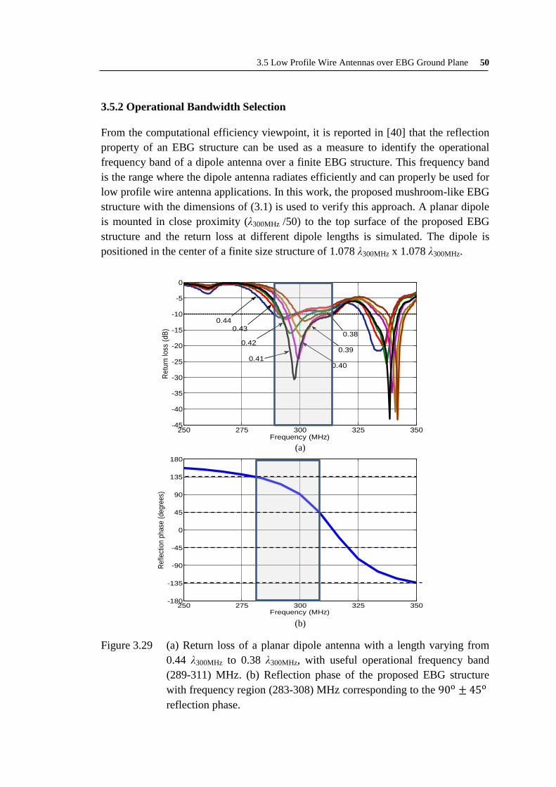
3.5 Low Profile Wire Antennas over EBG Ground Plane 50
3.5.2 Operational Bandwidth Selection From the computational efficiency viewpoint, it is reported in [40] that the reflection property of an EBG structure can be used as a measure to identify the operational frequency band of a dipole antenna over a finite EBG structure. This frequency band is the range where the dipole antenna radiates efficiently and can properly be used for low profile wire antenna applications. In this work, the proposed mushroom-like EBG structure with the dimensions of (3.1) is used to verify this approach. A planar dipole is mounted in close proximity (λ300MHz /50) to the top surface of the proposed EBG structure and the return loss at different dipole lengths is simulated. The dipole is positioned in the center of a finite size structure of 1.078 λ300MHz x 1.078 λ300MHz.
Figure 3.29 (a) Return loss of a planar dipole antenna with a length varying from 0.44 λ300MHz to 0.38 λ300MHz, with useful operational frequency band (289-311) MHz. (b) Reflection phase of the proposed EBG structure with frequency region (283-308) MHz corresponding to the 90o ± 45o
reflection phase.
250 275 300 325 350-180
-135
-90
-45
0
45
90
135
180
Frequency (MHz)
Refle
ction
pha
se (d
egre
es)
250 275 300 325 350-45
-40
-35
-30
-25
-20
-15
-10
-5
0
Frequency (MHz)
Retu
rn lo
ss (d
B)
0.40
0.38
0.390.41
0.42
0.440.43
(a)
(b)

51 3 Characterization of EBG Structures
Figure 3.29a shows the return loss of a wire dipole antenna with its length varying from 0.44 λ300MHz to 0.38 λ300MHz. According to the S1,1 ˂ -10dB return loss criterion, the useful operational frequency band of the dipole model is seen from 289 MHz to 311 MHz (7.33%).
The question was, is it possible to avoid the high computational effort of the full model simulation and to estimate the operational frequency band of the dipole model from a reflection phase region of the plane wave model of the EBG structure.
Figure 3.29b shows the reflection coefficient phase of the proposed EBG structure. It is observed that the frequency region (283 - 308) MHz which is corresponding to the quadratic phase (90o ± 45o) reflection coefficient is very close to the operational frequency band of a dipole model. Thus, quadrature reflection phase is very useful for a low profile wire antenna to obtain a good return loss. The reflection coefficient curve in Fig. 3.29b exhibits another frequency region that can satisfy good return loss for the dipole; this region is corresponding to the quadratic phase (−90o ±45o) reflection coefficient.
In conclusion, Fig. 3.29 describes the consistency between the frequency band of the dipole model and the frequency band of the plane wave model that satisfy good return loss and efficient radiation for low profile wire antenna applications.
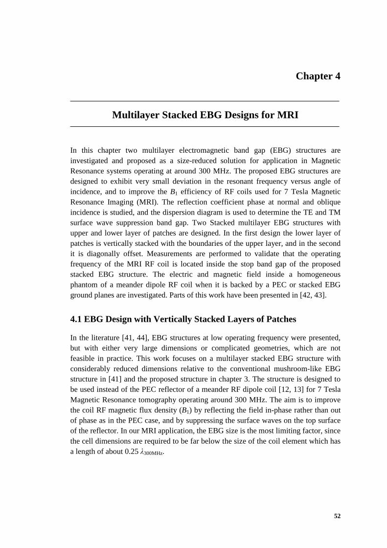
Chapter 4
Multilayer Stacked EBG Designs for MRI
In this chapter two multilayer electromagnetic band gap (EBG) structures are investigated and proposed as a size-reduced solution for application in Magnetic Resonance systems operating at around 300 MHz. The proposed EBG structures are designed to exhibit very small deviation in the resonant frequency versus angle of incidence, and to improve the B1 efficiency of RF coils used for 7 Tesla Magnetic Resonance Imaging (MRI). The reflection coefficient phase at normal and oblique incidence is studied, and the dispersion diagram is used to determine the TE and TM surface wave suppression band gap. Two Stacked multilayer EBG structures with upper and lower layer of patches are designed. In the first design the lower layer of patches is vertically stacked with the boundaries of the upper layer, and in the second it is diagonally offset. Measurements are performed to validate that the operating frequency of the MRI RF coil is located inside the stop band gap of the proposed stacked EBG structure. The electric and magnetic field inside a homogeneous phantom of a meander dipole RF coil when it is backed by a PEC or stacked EBG ground planes are investigated. Parts of this work have been presented in [42, 43].
4.1 EBG Design with Vertically Stacked Layers of Patches In the literature [41, 44], EBG structures at low operating frequency were presented, but with either very large dimensions or complicated geometries, which are not feasible in practice. This work focuses on a multilayer stacked EBG structure with considerably reduced dimensions relative to the conventional mushroom-like EBG structure in [41] and the proposed structure in chapter 3. The structure is designed to be used instead of the PEC reflector of a meander RF dipole coil [12, 13] for 7 Tesla Magnetic Resonance tomography operating around 300 MHz. The aim is to improve the coil RF magnetic flux density (B1) by reflecting the field in-phase rather than out of phase as in the PEC case, and by suppressing the surface waves on the top surface of the reflector. In our MRI application, the EBG size is the most limiting factor, since the cell dimensions are required to be far below the size of the coil element which has a length of about 0.25 λ300MHz.
52
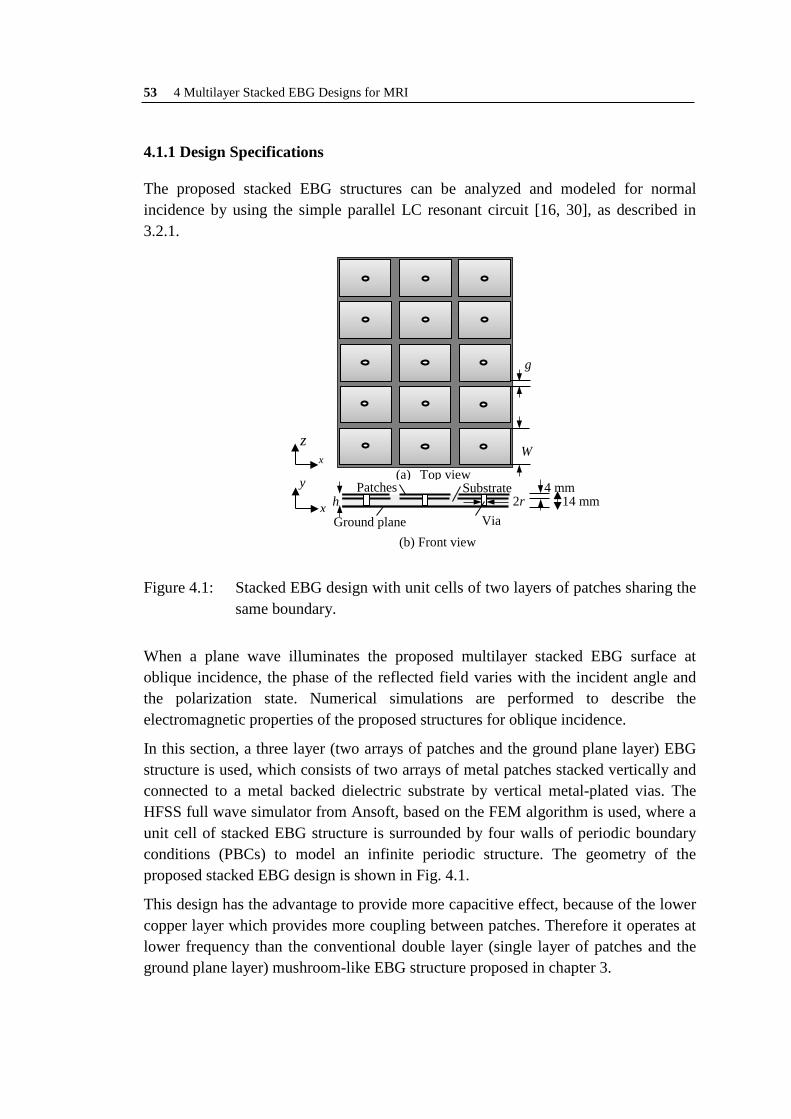
53 4 Multilayer Stacked EBG Designs for MRI
4.1.1 Design Specifications
The proposed stacked EBG structures can be analyzed and modeled for normal incidence by using the simple parallel LC resonant circuit [16, 30], as described in 3.2.1.
Figure 4.1:
Stacked EBG design with unit cells of two layers of patches sharing the same boundary.
When a plane wave illuminates the proposed multilayer stacked EBG surface at oblique incidence, the phase of the reflected field varies with the incident angle and the polarization state. Numerical simulations are performed to describe the electromagnetic properties of the proposed structures for oblique incidence.
In this section, a three layer (two arrays of patches and the ground plane layer) EBG structure is used, which consists of two arrays of metal patches stacked vertically and connected to a metal backed dielectric substrate by vertical metal-plated vias. The HFSS full wave simulator from Ansoft, based on the FEM algorithm is used, where a unit cell of stacked EBG structure is surrounded by four walls of periodic boundary conditions (PBCs) to model an infinite periodic structure. The geometry of the proposed stacked EBG design is shown in Fig. 4.1.
This design has the advantage to provide more capacitive effect, because of the lower copper layer which provides more coupling between patches. Therefore it operates at lower frequency than the conventional double layer (single layer of patches and the ground plane layer) mushroom-like EBG structure proposed in chapter 3.
Patches Substrate 2r
Via
(a) Top view
Ground plane (b) Front view
W
g
h
z x
x
y 4 mm 14 mm

4.1 EBG Design with Vertically Stacked Layers of Patches 54
The electromagnetic properties of the EBG structures are characterized by the patch width W, gap width g, dielectric constant εr, substrate thickness h, and vias radius r with the following design data shown in (4.1):
W = 0.072 λ300MHz, g = 0.001 λ300MHz, h = 0.014 λ300MHz, 𝜀𝑟 = 10.2, and r = 0.00173 λ300MHz.
(4.1)
Here, λ300MHz is the free-space wavelength at 300 MHz, which is used as a reference length to define the physical dimensions of the analyzed structure. The spacing between the two layers of patches in the proposed structure was chosen to be 0.004 λ300MHz. The new proposed design with the lower layer of patches exhibits more than 25% reduction in the unit cell size dimension compared to the conventional EBG structure presented in chapter 3.
4.1.2 Resonance Insensitivity of the Multilayer EBG Design In this part, the stacked EBG structure is designed so that the MRI operating frequency is located inside the frequency band where the reflection phase is in the range of 90o ± 45o, which is helpful for low profile antennas to achieve good return loss [40], as shown in Ch. 3.5.
The sensitivity of the proposed stacked EBG structure is investigated by determining the deviation in the resonant frequency against different angles of plane wave incidence. Plane waves are illuminating the stacked EBG surface based on the dimensions in (4.1), and the transverse electric (TE) and transverse magnetic (TM) reflection coefficient phases for normal and oblique incidence in the presence and absence of vias are analyzed and presented as shown below.
4.1.2.1 Reflection Phase for TE and TM Plane Waves in the Presence and Absence of Vias For a TE-polarized plane wave obliquely illuminating the stacked EBG structure in the presence of vias, the resonance frequency increases with the increase of the incidence angle, as shown in Fig. 4.2a. The change in resonant frequency for the angle of incidence varying from 0O to 70O is only about 3%, which represents a very high resonance insensitivity against oblique incidence for the proposed stacked EBG structure. In the absence of vias, exactly the same effect is exhibited, as shown in Fig. 4.2b, because for TE-polarization the electric field is always parallel to the EBG surface and the vias are not excited.
For a TM-polarized plane wave obliquely illuminating the same structure in the presence of vias, dual resonance behavior is observed. This phenomenon is also observed for the conventional mushroom-like EBG structure in [29, 40].
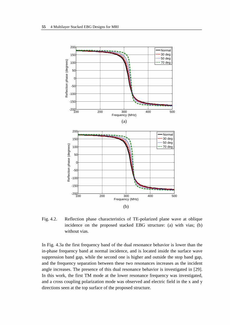
55 4 Multilayer Stacked EBG Designs for MRI
In Fig. 4.3a the first frequency band of the dual resonance behavior is lower than the in-phase frequency band at normal incidence, and is located inside the surface wave suppression band gap, while the second one is higher and outside the stop band gap, and the frequency separation between these two resonances increases as the incident angle increases. The presence of this dual resonance behavior is investigated in [29]. In this work, the first TM mode at the lower resonance frequency was investigated, and a cross coupling polarization mode was observed and electric field in the x and y directions seen at the top surface of the proposed structure.
100 200 300 400 500-200
-150
-100
-50
0
50
100
150
200
Frequency (MHz)
Ref
lect
ion
phas
e (d
egre
es)
Normal30 deg50 deg70 deg
100 200 300 400 500-200
-150
-100
-50
0
50
100
150
200
Frequency (MHz)
Ref
lect
ion
phas
e (d
egre
es)
Normal30 deg50 deg70 deg
Fig. 4.2.
Reflection phase characteristics of TE-polarized plane wave at oblique incidence on the proposed stacked EBG structure: (a) with vias; (b) without vias.
(b)
(a)
4.1 EBG Design with Vertically Stacked Layers of Patches 56
Figure 4.3: Reflection phase characteristics of TM-polarized plane wave at oblique
incidence on the proposed stacked EBG structure: (a) dual resonant behavior in the presence of vias (b) single resonant behavior in the absence of vias.
The excitation of this mode depends on the existence of the vias. When there are no conducting vias in the structure, the dual resonant behavior disappears and the resonant frequency corresponding to zero degree reflection phase increases with the incidence angle of the TM plane wave, as shown in Fig. 4.3b.
100 200 300 400 500-200
-150
-100
-50
0
50
100
150
200
Frequency (MHz)
Ref
lect
ion
phas
e (d
egre
es)
Normal30 deg.50 deg.70 deg.
100 200 300 400 500-200
-150
-100
-50
0
50
100
150
200
Frequency (MHz)
Ref
lect
ion
phas
e (d
egre
es)
Normal30 deg.50 deg.70 deg.
(a)
(b)

57 4 Multilayer Stacked EBG Designs for MRI
4.1.2.2 The Dispersion Diagram in the Presence and Absence of Vias The dispersion diagram in Fig. 4.4a shows a stop band gap between the first two modes (TM mode and TE mode respectively) which is obtained in the frequency range (286 MHz - 325 MHz). The proposed EBG structure is designed so that the frequency range of the stop band gap is very close to the frequency band where the structure shows a reflection phase in the range of 90o ± 45o.
Figure 4.4:
Dispersion diagram of the proposed EBG structure: (a) when vias of radius 1.73 mm are used; (b) In the absence of vias, where no surface wave band gap is exist.
The stop band gap property of the EBG structure was validated using an open air-filled microstrip transmission line which is loaded by a finite 3x5 unit cells EBG structure, as will be discussed later in this chapter.
100
200
300
400
500
600
700
Wavenumber( )
Freq
uenc
y (M
Hz)
First modeSecond mode)Third modeFourth modelight line
100
200
300
400
500
600
700
800
900
Wavenumber(b)
Freq
uenc
y (Hz
)
First modeSecond modeThird modeFourth modelight line
No Surface Wave Bandgap
Γ Γ M X
(a) Wavenumber Γ Γ M X
Wavenumber
(b)

4.2 Offset Layers Stacked EBG Design 58
Figure 4.5
FDTD simulation result of the transmission (S2,1) scattering coefficient of the proposed stacked EBG structure.
The loaded microstrip with the proposed EBG structure was simulated using the FDTD Empire XCcel, and the transmission scattering coefficient S2,1 result is shown in Fig. 4.5.
Figure 4.5 proofs that our MRI operating frequency is located inside the stop band gap through which the surface waves are suppressed and also inside the frequency range (the shadow area) corresponding to that range of the quadratic phase reflection coefficient which is very helpful for low profile wire antenna applications to achieve good return loss. In the absence of vias, Fig. 4.5 shows that the stop band gap disappears in a similar manner as shown in Fig. 4.4b.
4.2 Offset Layers Stacked EBG Design In this part of the thesis, our first application of an EBG structure [43] to improve the B1 efficiency of RF coils used for 7 Tesla Magnetic Resonance Imaging (MRI) is introduced. The proposed offset multilayer stacked EBG structure is used as high impedance surface behind an extended half-wavelength meandered dipole, as shown in Fig. 4.6. It operates at about 300 MHz, the magnetic resonance frequency at 7Tesla.
The novel approach presented in this work has the objective to increase the B1 efficiency of a well-established RF coil [13] by replacing the PEC ground plane with an EBG structure. Therefore the anti-phase currents can be avoided and surface waves are suppressed and the magnetic flux density inside the load is increased.
The condition for a successful application of the EBG structure in MRI is unique in that the cell dimensions are required to be far below the size of the meander dipole
0 50 100 150 200 250 300 350 400 450 500-30
-25
-20
-15
-10
-5
0
5
Frequency (MHz)
Tran
smis
sion
(S2,
1) C
oeffi
cien
t (dB
)
s2,1(with vias)s2,1(without vias)

59 4 Multilayer Stacked EBG Designs for MRI
coil, which in our case is 25% of the free-space wavelength. Thus, this section focuses on a multi-layer stacked EBG structure with a lateral cell size less than 7.7 % of lambda. The coupling capacitance available with this offset layers stacked design compared to the previous vertical stacked layers design enable us to reduce the thickness of the dielectric substrate from 14 mm to only 6.4 mm.
4.2.1 Design Specifications When a plane wave illuminates a symmetric EBG unit cell at normal incidence, the reflection phase is independent of the polarization state, and can be used to define the band-gap feature [16].
Figure 4.6
Offset layers stacked EBG design, with a layer of patches diagonally offset from the upper one. A meandered dipole sits 2 cm above the top surface of the proposed EBG structure.
The structure can be modeled analytically by using the simple parallel LC resonant circuit, described in 3.2.1. In the present design, a stacked EBG structure is used, which consists of two arrays of metal patches with a diagonal offset from each other. The top layer is connected to the metal backing of the dielectric substrate by vertical metal-plated vias, while the lower one is floating. The HFSS full wave simulator, based on the FEM algorithm with periodic boundary conditions (PBCs) is used to design and characterize one unit cell of the EBG structure, and the FDTD simulator EMPIRE XCcel is used to analyze the finite EBG structure. The geometry of the proposed finite offset layers stacked EBG structure together with the meander dipole coil above the analyzed structure is shown in Fig 4.6.
x
(a) Top view
(b) Front view
y x
z
h2 h1

4.2 Offset Layers Stacked EBG Design 60
The physical dimensions of the proposed EBG structure are initialized as in (4.2):
W = 0.07475 λ300MHz, g = 0.002 λ300MHz, h1=h2 = 0.032 λ300MHz, 𝜀𝑟 = 10.9, and r = 0.003 λ300MHz.
(4.2)
The dimensions were chosen with the availability of dielectric laminates in mind. Arlon (Arlon corp. of USA) substrates with overall height h = 6.4 mm are assumed. The spacing between the two layers of patches was chosen to be 0.0032 λ300MHz due to the availability of laminates of 3.2 mm thickness. During fabrication of this structure a thin dielectric film of permittivity 4.4 and 0.2 mm thickness was used to join the two Arlon substrates together. This layer is also modelled in the simulation.
A resonant meandered dipole is used as RF-transmit coil in 7 Tesla MRI (with extended folded arms to resonate at 300 MHz), etched on FR4 epoxy substrate of 0.5 mm thickness and mounted above the EBG structure so that the total height of the configuration is 20 mm, same as the original coil construction including a PEC ground plane.
4.2.2 Reflection Phase and Dispersion Diagram For a plane wave illuminating the proposed offset stacked EBG unit cell based on the dimensions given in (4.2) at normal incidence, the reflection coefficient phase is shown in the solid line of Fig. 4.7. The proposed structure is designed to resonate at the MRI system frequency (300 MHz). The resonant frequency is designed so that it is located inside the frequency band where the reflection phase is in the range of ±90O in order to reflect the fields in-phase rather than out of phase as in the PEC case. In this design, the EBG structure resonates corresponding to 0Oreflection phase and satisfies the artificial magnetic conductor (AMC) property.
When the offset stacked EBG design is used with the dimensions of (4.1), the resonant frequency corresponding to zero degree reflection phase reduces to 204 MHz. Thus, the offset layers stacked EBG design is capable to reduce the resonant frequency by 35% relative to the vertical stacked EBG design, because it provides more coupling between the adjacent patches. In contrast, if the lower layer of the EBG patches described in (4.2) is vertically stacked with the upper one, the resultant reflection coefficient phase exhibits that the resonance is up shifted in frequency by an amount reaching 65%, as shown in the dotted line in Fig. 4.7.
Additionally to the reflection phase property, the proposed EBG structure can be characterized by its dispersion diagram, as shown in Fig. 4.8. This information includes the surface wave characteristics.

61 4 Multilayer Stacked EBG Designs for MRI
Figure 4.7 Reflection phase of the proposed offset and vertically stacked EBG structure based on the dimension in (4.2).
Figure 4.8 Dispersion diagram of the proposed offset stacked EBG structure.
The dispersion diagram in this work is calculated using the eigenmode solver of the FEM based algorithm HFSS simulator. It shows the frequency bands through which propagation of the surface waves are suppressed. A stop band gap between the first two modes (TM mode and TE mode respectively) is observed in the frequency range (275 MHz – 315 MHz), as shown in Fig. 4.8. It is ensured that our MRI operating frequency is located inside this stop band gap.
100 150 200 250 300 350 400 450 500-200
-150
-100
-50
0
50
100
150
200
Frequency (MHz)
Ref
lect
ion
phas
e (d
egre
es)
Offset stacked layersVertically stacked layers
0
100
200
300
400
500
600
700
800
900
Freq
uenc
y (M
Hz)
Wavenumber
First mode Second mode Third mode Fourth mode lightline
Band gap
M X Γ Γ
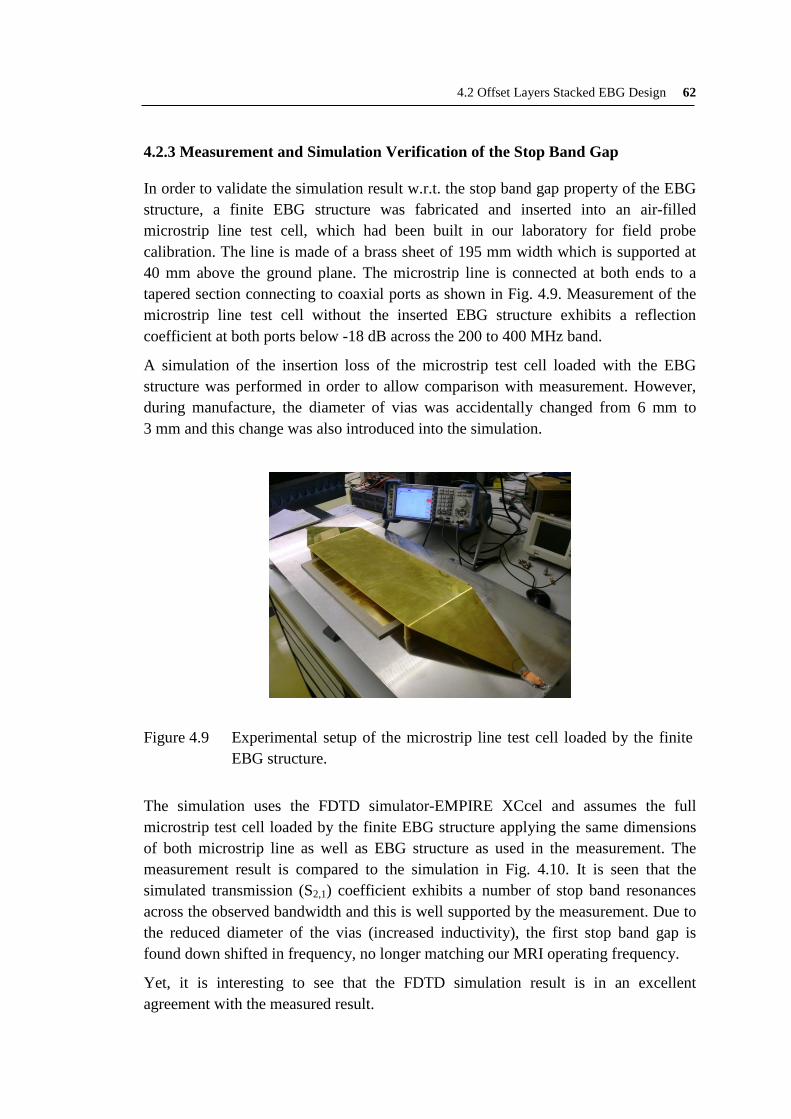
4.2 Offset Layers Stacked EBG Design 62
4.2.3 Measurement and Simulation Verification of the Stop Band Gap In order to validate the simulation result w.r.t. the stop band gap property of the EBG structure, a finite EBG structure was fabricated and inserted into an air-filled microstrip line test cell, which had been built in our laboratory for field probe calibration. The line is made of a brass sheet of 195 mm width which is supported at 40 mm above the ground plane. The microstrip line is connected at both ends to a tapered section connecting to coaxial ports as shown in Fig. 4.9. Measurement of the microstrip line test cell without the inserted EBG structure exhibits a reflection coefficient at both ports below -18 dB across the 200 to 400 MHz band.
A simulation of the insertion loss of the microstrip test cell loaded with the EBG structure was performed in order to allow comparison with measurement. However, during manufacture, the diameter of vias was accidentally changed from 6 mm to 3 mm and this change was also introduced into the simulation.
Figure 4.9 Experimental setup of the microstrip line test cell loaded by the finite EBG structure.
The simulation uses the FDTD simulator-EMPIRE XCcel and assumes the full microstrip test cell loaded by the finite EBG structure applying the same dimensions of both microstrip line as well as EBG structure as used in the measurement. The measurement result is compared to the simulation in Fig. 4.10. It is seen that the simulated transmission (S2,1) coefficient exhibits a number of stop band resonances across the observed bandwidth and this is well supported by the measurement. Due to the reduced diameter of the vias (increased inductivity), the first stop band gap is found down shifted in frequency, no longer matching our MRI operating frequency.
Yet, it is interesting to see that the FDTD simulation result is in an excellent agreement with the measured result.

63 4 Multilayer Stacked EBG Designs for MRI
Figure 4.10
Measurement result and FDTD simulated transmission (S2,1) coefficient of the proposed offset stacked EBG structure.
Figure 4.11 (a) EBG structure with vias diameter increased to 6 mm, (b) Measured
transmission (S2,1) coefficient (dB).
This correspondence between measurement and simulation results allows us to design the stop band gap of the EBG structures confidently and very accurately, as will be seen in chapter 6.
The vias diameters of the proposed EBG structure were increased, by drilling, to the previous designed value in (4.2), as shown in Fig. 4.11a. The transmission coefficient result was measured again using the microstrip line method.
100 150 200 250 300 350 400 450 500-35
-30
-25
-20
-15
-10
-5
0
5
Frequency (MHz)
Tran
smis
sion
coe
ffici
ent (
dB)
Measured S2,1Empire S2,1
100 200 300 400 500-20
-15
-10
-5
0
5
Frequency (MHz)
Tran
smiss
ion
coef
ficie
nt (d
B)
(a) (b)

4.2 Offset Layers Stacked EBG Design 64
Figure 4.12 EBG structure with two layers of patches and vias.
Figure 4.13: FDTD result of the transmission (S2,1) coefficient showing that the existence of a second layer of vias reduces the overall inductance and shifts the resonance up in frequency.
It is observed as shown in Fig. 4.11b, that the resonance is up shifted in frequency to the MRI operating frequency of 300 MHz. Thus, the resonant frequency increases when the diameters of the vias are increased. The thicker the radius of the vias is, the smaller is the inductance and hence the higher is the resonant frequency, as can analyzed from the resonant frequency equation (3.11) of parallel LC resonant circuits.
The effect of adding a new layer of vias to connect the lower layer of patches with the ground plane, as shown in Fig. 4.12, was also investigated. The FDTD simulation result shows that the resonant frequency of the new EBG structure increases when this
0 50 100 150 200 250 300 350 400 450 500-35
-30
-25
-20
-15
-10
-5
0
5
Frequency (MHz)
Tran
smis
sion
coe
ffici
ent (
dB)
S2,1(One layer of vias)S2,1(Two layers of vias)
(a)Top view
(b) Front view x
y x
z

65 4 Multilayer Stacked EBG Designs for MRI
layer of vias is added, as shown in Fig. 4.13. That means, adding the new layer of vias not only increases the complexity of the design but also reduces the overall inductance of the EBG structure. This is explained in the parallel LC resonant circuit of the EBG structure by another inductor connected in parallel with the inductor from the first layer of vias.
4.2.4 Application to MRI: Meander Dipole over aOffset Stacked EBG Structure The performance of the original coil configuration based on a meandered dipole over a PEC ground plane is compared to the performance when it is over the proposed multilayer offset stacked EBG structure. The comparison is done by simulating the magnetic distribution inside a homogeneous phantom (length = 305 mm, width = 154 mm, height = 100 mm, εr = 40, σ = 0.8 S/m) placed 2 cm above the coil. In order to compare in a fair manner, all values have been normalized to the square root of the accepted RF power.
The distribution of the magnetic field inside the phantom and at different vertical distances in the y - axis (from the bottom-center to the top-center) is shown in Fig. 4.14. As can be seen from Fig. 4.14, the maximum normalized magnetic field intensity in the presence of the proposed EBG structure is 2.266 A/m/√W while the value reduces to 1.538 A/m/√W when a PEC ground plane of the same size (305 mm x 305 mm) is used. That means, the presence of the proposed EBG structure enhances the B1-field by about 47% compared to the PEC case.
Figure 4.14 FDTD simulation result of absolute magnetic field inside the phantom along the vertical direction, from the bottom-center to the top- center of the phantom. y = 0 is at the bottom of the phantom.
0 20 40 60 80 1000
0,3
0,6
0,9
1,2
1,5
1,8
2.12,266
2,4
Vertical distance, Y [mm]
Nor
mal
ized
| H
|
EBGPEC

4.3 Conclusion 66
It is clear from this longitudinal field distribution that the maximum normalized magnetic field at any height is always at the center, as it also is in the case of the coil over the PEC ground plane.
The absolute normalized magnetic field intensity distribution in the longitudinal direction and at different distances inside the phantom is also investigated for the case when the coil is backed by the proposed EBG structure. Figure 4.15 shows that the longitudinal magnetic field distribution exhibits a symmetric variation with a peak in the centre, above the centre of the dipole; this is the same as in the case of the PEC ground plane. The associated field characteristic as we go up inside the phantom (along the vertical axis) exhibits the same lowering behavior as shown in Fig. 4.14.
4.3 Conclusion A vertical and an offset multilayer stacked EBG structures are proposed to work at the MRI operating frequency of 300 MHz, with relatively small electrical dimensions compared to the conventional mushroom-like EBG structures. The reflection phase and surface wave suppression band gap properties of the proposed structures are investigated. The vertically stacked EBG structure exhibits very small deviation in the resonant frequency for angle of incidence varying from 0o − 70o (less than 3%), and exhibits a surface wave suppression band gap correlated to the quadrature reflection phase criterion 90o ± 45o. When a TM-polarized plane wave obliquely illuminates the proposed structure, a dual resonant behavior is observed, with a lower in-phase frequency band located inside the realized stop band gap (286 MHz - 325 MHz).
0 61 122 152.5 183 244 3050
0.2
0.4
0.6
0.8
1
1.2
Longitudinal distance, Z (mm)
Nor
mal
ized
| H
|
20 mm40 mm60 mm80 mm100 mm
Figure 4.15: FDTD results of longitudinal normalized magnetic field at different heights inside the phantom (using EBG structure).

67 4 Multilayer Stacked EBG Designs for MRI
An offset multilayer stacked EBG structure is designed to work as an artificial magnetic conductor (AMC). The structure resonates at the MRI operating frequency corresponding to a zero degree phase reflection coefficient. Thus, the structure reflects the field in-phase rather than out of phase as in the PEC ground planes. The proposed structure is fabricated and its stop band gap is validated by measurements. These unique properties make the proposed EBG structure a good candidate for a ground plane in a 7 Tesla Magnetic Resonance (MR) coil providing good reflection and good suppression of surface waves on the ground plane. The proposed offset stacked EBG structure comprises of electrically small cells of only 7.7% of the free-space wavelength and resonates lower than the vertically stacked EBG design by 65%, when the same dimensions are used. The MRI meander dipole coil backed by our EBG structure is successful in exhibiting a stronger B1-field inside a phantom than the original design using a metallic conductor (PEC) ground plane for the coil. The quantitative improvement in B1 efficiency amounts to 47%.
Chapter 5
Miniaturization and Tuning of EBG Structures
Miniaturization of EBG structures can be achieved by using different techniques. These include the use of more complex frequency selective surfaces FSSs, using EBG substrates with efficient properties, changing the symmetry of the EBG surface to change the polarization, and using extra components to the designed EBG structure.
A considerable amount of literature has been published on miniaturization techniques based on the compact EBG design, including the space filling curves like Peano and Hilbert curves [45-50], where the electrical length is packed in a fixed available space. Any geometry that elongates the path through which the currents pass, like the slotted and spiral EBG designs [51, 52], is in general helpful for miniaturization. These complicated geometries focus on the compactness of the EBG surface to increase mainly the inductance, and resulting in a lower resonant frequency. Miniaturization can also be realized by employing closely coupling arrays of patches in a multilayer configuration, as described in chapter 4. Using some dielectric substrates which have efficient and abnormal properties, like the high permeability magneto-dielectric sheets [53] was found useful to shift the resonance down in frequency and to increase the bandwidth. Miniaturization is also achieved when polarization-dependent EBG structures are designed, by using asymmetric geometries such as rectangular shape of patches or offset vias [54].
Another technique of miniaturization is based on using extra components to the EBG structure, as the lumped elements and diodes [55]. Adding extra components to the EBG structure is usually a method used for tuning purposes. In this chapter some promising tuning techniques are also introduced which depend on connecting extra parts to the EBG structure to change its equivalent inductance and capacitance, and as a result shift its resonant frequency. These techniques include an adjustable air-gap layer with pins connected to the bottom surface of the EBG structure, and coaxial cables connected with the vias.
In this chapter, the possibility to use a miniaturized and tuned EBG structure based on the aforementioned techniques or mix of them to satisfy the limited size and functionality requirements in MRI applications will be explained and numerically investigated.
68

69 5 Miniaturization and Tuning of EBG Structures
5.1 Magneto-Dielectric Material Magneto-Dielectric materials have been used widely for miniaturizations of antennas and EBG structures [53]. These kinds of substrates have a permeability µr greater than one. It is known from [16] that the parallel LC resonant circuit has a bandwidth corresponding to the in-phase reflection bandwidth which is proportional to �𝐿 𝐶⁄ , and it has a resonance frequency proportional to 1/√𝐿𝐶. The magneto-dielectric material increases the inductance L of the EBG structure as the permeability µr increases, as can be seen from (3.14). Accordingly, the bandwidth increases and the resonance is shifted down in frequency. Miniaturization can also be achieved using dielectric materials with high dielectric constants, but according to (3.12) and the aforementioned relations, the reduction in the resonant frequency will be accompanied with a clear reduction in the bandwidth.
Magneto-dielectric substrates have the advantage to miniaturize EBG structures; they allow us to shrink the patch size, decrease the substrate thickness, and to use EBG substrate of small relative permittivity. Depending on the value of the permeability, the aforementioned goals can be achieved with the required resonant frequency and higher bandwidth than the conventional dielectric substrates.
The offset stacked EBG structure which was proposed in chapter 4 to resonate at 300 MHz is used here as a reference EBG structure, it has the following unit cell dimensions:
W = 0.07467 λ300MHz, g = 0.002 λ300MHz, h1 = h2 = 0.0032 λ300MHz, 𝜀𝑟 = 10.9, and r = 0.004 λ300MHz.
(5.1)
Here, λ300MHz is used as a reference length, W is the solid patch width, g is the gap width, h1 and h2 represent the thicknesses of the Arlon A-1000 substrates of 10.9 relative dielectric constant. A 200 micron dielectric layer of permittivity 4.4 is inserted between the two aforementioned substrates to model the tape used to bond them together.
In this section, an EBG structure with the same dimensions of the above reference EBG structure is used, and only the dielectric substrates are replaced with a magneto-dielectric substrate of the same relative permittivity 𝜀𝑟 = 10.9 but with different relative permeability µr = 10.9. A comparison is taken between the reflection coefficient phase of the proposed EBG structure with the magneto-dielectric substrate and the reference EBG structure.
As shown in Fig. 5.1a, the first resonant frequency of the reference EBG structure is reduced from 300 MHz to 91 MHz when the same unit cell dimensions and patch geometries are used now with magneto-dielectric substrate of µr = 10.9.
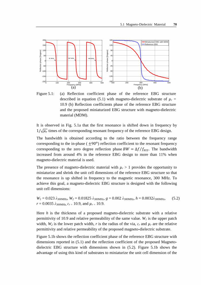
5.1 Magneto-Dielectric Material 70
Figure 5.1: (a) Reflection coefficient phase of the reference EBG structure described in equation (5.1) with magneto-dielectric substrate of µr = 10.9 (b) Reflection coefficients phase of the reference EBG structure and the proposed miniaturized EBG structure with magneto-dielectric material (MDM).
It is observed in Fig. 5.1a that the first resonance is shifted down in frequency by 1/√𝜇𝑟 times of the corresponding resonant frequency of the reference EBG design.
The bandwidth is obtained according to the ratio between the frequency range corresponding to the in-phase ( ±90o) reflection coefficient to the resonant frequency corresponding to the zero degree reflection phase 𝐵𝑊 = ∆𝑓 𝑓𝐻𝐼𝑆⁄ . The bandwidth increased from around 4% in the reference EBG design to more than 11% when magneto-dielectric material is used.
The presence of magneto-dielectric material with µr > 1 provides the opportunity to miniaturize and shrink the unit cell dimensions of the reference EBG structure so that the resonance is up shifted in frequency to the magnetic resonance, 300 MHz. To achieve this goal, a magneto-dielectric EBG structure is designed with the following unit cell dimensions:
W1 = 0.023 λ300MHz, W2 = 0.01825 λ300MHz, g = 0.002 λ300MHz, h = 0.0032λ300MHz, r = 0.0035 λ300MHz, ɛr = 10.9, and µr = 10.9.
(5.2)
Here h is the thickness of a proposed magneto-dielectric substrate with a relative permittivity of 10.9 and relative permeability of the same value. W1 is the upper patch width, W2 is the lower patch width, r is the radius of the via, ɛr and µr are the relative permittivity and relative permeability of the proposed magneto-dielectric substrate.
Figure 5.1b shows the reflection coefficient phase of the reference EBG structure with dimensions reported in (5.1) and the reflection coefficient of the proposed Magneto-dielectric EBG structure with dimensions shown in (5.2). Figure 5.1b shows the advantage of using this kind of substrates to miniaturize the unit cell dimension of the
0 100 200 300 400 500-200
-150
-100
-50
0
50
100
150
200
Frequency [MHz]
Ref
lect
ion
phas
e [D
egee
s]
91 MHz 267 MHz 446 MHz
100 200 300 400 500-180
-135
-90
-45
0
45
90
135
180
Frequency [MHz]
Ref
lect
ion
phas
e [D
egee
s]
Miniaturized EBG with MDMReference EBG
(a) (b)
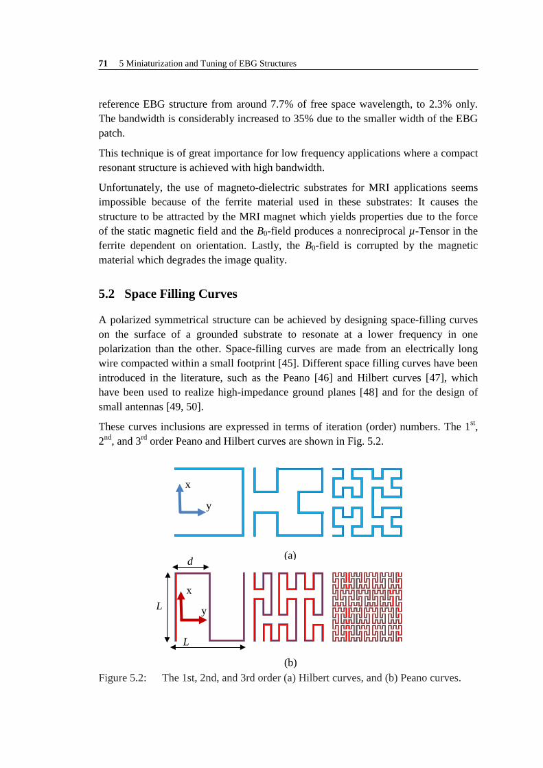
71 5 Miniaturization and Tuning of EBG Structures
reference EBG structure from around 7.7% of free space wavelength, to 2.3% only. The bandwidth is considerably increased to 35% due to the smaller width of the EBG patch.
This technique is of great importance for low frequency applications where a compact resonant structure is achieved with high bandwidth.
Unfortunately, the use of magneto-dielectric substrates for MRI applications seems impossible because of the ferrite material used in these substrates: It causes the structure to be attracted by the MRI magnet which yields properties due to the force of the static magnetic field and the B0-field produces a nonreciprocal µ-Tensor in the ferrite dependent on orientation. Lastly, the B0-field is corrupted by the magnetic material which degrades the image quality.
5.2 Space Filling Curves A polarized symmetrical structure can be achieved by designing space-filling curves on the surface of a grounded substrate to resonate at a lower frequency in one polarization than the other. Space-filling curves are made from an electrically long wire compacted within a small footprint [45]. Different space filling curves have been introduced in the literature, such as the Peano [46] and Hilbert curves [47], which have been used to realize high-impedance ground planes [48] and for the design of small antennas [49, 50].
These curves inclusions are expressed in terms of iteration (order) numbers. The 1st, 2nd, and 3rd order Peano and Hilbert curves are shown in Fig. 5.2.
`
Figure 5.2: The 1st, 2nd, and 3rd order (a) Hilbert curves, and (b) Peano curves.
(a)
(b)
x
y
L
d
x
y
L

5.2 Space Filling Curves 72
Table 5.1: Total length S for Peano and Hilbert curves with respect to iteration order number N. L is the linear side dimension of the curve.
Peano Curve S=(32N-1)d d=L/(3N-1)
Hilbert Curve S=(22N-1)d d=L/(2N-1)
Table 5.1 illustrates the total length S of the Hilbert and Peano wires as a function of the iteration order number N for the same footprint size [56]. The advantage of these curves for elongating the wire length while maintaining the same footprint size (L x L) make them useful to design planar high impedance surfaces with long resonant wavelength and hence low resonant frequency. Figure 5.2 and Table 5.1 show that for a fixed order N and square unit cells of the same footprint the Peano curve has higher compression rate than the Hilbert curve.
Design Parameters of Hilbert and Peano Curves In this part, the resonant frequency of various iteration orders of Peano and Hilbert curve elements were simulated using the FEM simulator HFSS with periodic boundary conditions (PBCs) surrounding each unit cell to model an infinite curve elements. A plane wave at normal incidence in free space with two different polarizations, i.e. Ex and Ey, was used to illuminate different unit cells of different orders, each contained within a footprint size (L x L) of 76.75 mm x 76.75 mm. The same unit cell dimensions of (5.1) are used.
To compare in a fair manner, the dimensions of the refence EBG structure shown in equation (5.1) were used, but the solid patch has been replaced with space filling curve elements of different iteration orders N while the same footprint size has been maintained. In this work, each curve element was modeled with a thin metallic strip of 2 mm width.
Resonant frequency and bandwidth are defined as given in section 5.1.
5.2.1 Resonances and Bandwidths of Hilbert Curves-EBG Structures In this section, the resonant frequency and bandwidth of EBG structures for different iteration order N Hilbert curves and at different polarizations are investigated. Figure 5.3 shows the x and y-polarized reflection coefficients phase of an EBG structure based on the 1st iteration order Hilbert curve.

73 5 Miniaturization and Tuning of EBG Structures
Figure 5.3: x and y-polarized reflection coefficients phase of the first order Hilbert curve EBG structure.
The proposed Hilbert curve EBG structure has the same unit cell dimensions of our reference solid patch geometry offset stacked EBG structure [43], which is described in equation (5.1). The use of this curve element with the same footprint will increase the length of the wire and hence elongate the path through which the currents pass, mainly for the x-polarized case. Accordingly, the wire inductance and the coupling capacitance increase, and the resonant frequency decreases.
As can be seen from Fig. 5.3, the resonant frequency for the x-directed polarization is lower than that for the y-directed polarization. This is mainly due to the symmetry of the Hilbert curve elements along the y-axis (see Fig. 5.1) while the wire appears to the current electrically longer with respect to the x- directed polarization compared to the y-directed case.
Figure 5.4 illustrates the effect of increasing the order iteration number N on the resonant frequency. It is observed that the higher the order of the curve, the lower is the resonant frequency. Increasing the order N of the Hilbert curve element while maintaining the same footprint size leads to increase of the total length of the wire, which will further increase the wire inductance and coupling capacitance and hence decreases the resonant frequency. It is evident in Fig. 5.4 that this compactness in the resonant frequency is accompanied by a reduction in bandwidth, because the coupling capacitance between the compact wires and with the lower layer of patches have the dominant effect on the surface impedance of the parallel resonant circuit. Since the electrical path is seen longer by the current in the x-direction, therefore the resonant frequency in this direction is seen much lower than the resonant frequency in the y-direction.
0 100 200 300 400 500-200
-150
-100
-50
0
50
100
150
200
Frequency (MHz)
Ref
lect
ion
phas
e (d
egee
s)
X-polarizedY-polarized

5.2 Space Filling Curves 74
Figure 5.4: x and y-polarized resonant frequencies and bandwidths of EBG structures based on Hilbert curve inclusions of orders 1 to 3.
The effect of shrinking the footprint size of the proposed Hilbert curve EBG structures to resonate at the MRI operating frequency is seen in Fig. 5.5. Miniaturized Hilbert curves of different iteration orders N are proposed such that their x-polarized in-phase reflection coefficients (of the lower resonances) are shifted up, and their resonant frequency reaches the MRI operating frequency. The normalized dimensions
1 2 3100150200250300350400
Hilbert Order #
Res
onan
ce fr
eq. (
MH
z)
1 2 30
0.5
1
1.5
2
2.5
Hilbert Order #
Ban
dwid
th [%
]
Res. Freq. Y-pol.Res. Freq. X-pol.
B.W. Y-pol.B.W. X-pol.
1 2 32
4
6
8
10
Hilbert Order #
S
ide
Dim
ensi
on
(%
of R
es. L
ambd
a)
1 2 30
1
2
3
4
Hilbert Order #
Ban
dwid
th [%
]
Side Dimension Y-PolSide Dimension X-Pol.
B.W. Y-Pol.B.W. X-Pol.
Figure 5.5: Normalized side dimension and bandwidth of EBG structure based on Hilbert curve inclusions of orders 1 to 3. Normalization is with respect to the MRI resonant wavelength λRES in the x-polarized direction, and with respect to the y-polarized resonant wavelength.

75 5 Miniaturization and Tuning of EBG Structures
of the footprint size to the resonant bandwidth (λRES) for the x-polarization (always adjusted to 𝜆 = 1) and y-polarization are shown in the upper part of Fig. 5.5, and their corresponding bandwidths are illustrated in the lower part.
Fig. 5.5 shows that the normalized side dimension of the footprint decreases with increase of the order iteration number N, because smaller unit cell size is required with higher order inclusions, i.e. when longer wires are used. This result is accompanied as seen in the lower part of the figure by a reduction in the percentage bandwidth, because as expected the higher the order of the curve the lower is the bandwidth. It can be seen from the lower part of Fig. 5.5 that significant differences were observed between the percentages bandwidths for these miniaturized Hilbert curves and those proposed in Fig. 5.4 (more obvious for the y-directed polarization). The reason for such a result, and as described in (3.12), refers to the fact that the smaller the footprint size, the lower is the capacitance, and hence the higher is the bandwidth.
5.2.2 Resonances and Bandwidths of Peano Curves-EBG Structures Peano curves of different order iteration numbers N are used to build a frequency selective surface FSS with the same dimensions in (5.1) to resonate at lower frequency than the reference solid patch geometry offset stacked EBG structure [43], as introduced in chapter 4.
To evaluate the scattering properties of EBG structures based on Peano curve inclusions, the periodic FEM simulator HFSS is utilized. The Peano surface is illuminated at normal incident with a plane wave polarized in the x or y direction. The scattering properties are shown in the figures below.
The same material and physical dimensions were used here as those proposed for EBG structures based on Hilbert curves. The upper part of Fig. 5.6 shows the resonant frequency of EBG structures based on Peano curves of order 1 and 2 polarized in the x and y-direction. The lower part of the figure presents their corresponding bandwidths.
Figure 5.6 shows that the resonant frequency for the y-polarized direction is lower than the x-polarized direction, because the current sees the wire longer in the y-direction than the x-direction. The figure also shows that the higher the order of the Peano curve the lower is the frequency and the lower is the corresponding bandwidth.
A comparison with Hilbert curves reveals that Peano curves exhibit lower resonant frequency, because of the longer wire and hence more compactness of the proposed Peano inclusions when the same order and the same footprint size are used. The third order Peano curve is not included here, because its high compactness makes it difficult to correctly demonstrate the lower resonance.

5.2 Space Filling Curves 76
Figure 5.6: x and y-polarized wave incidence resonant frequency and bandwidth of EBG structures based on Peano curve inclusions of orders 1 and 2.
Figure 5.7: Normalized side dimension and bandwidth of EBG structures based on Peano curve inclusions of orders 1 and 2. Normalization is with respect to the MRI resonant wavelength λRES in the x-polarized direction, and with respect to the y-polarized resonant wavelength.
Figure 5.7 shows the unit cell size dimension of the proposed Peano surfaces as a percentage of their corresponding resonant wavelength. This figure shows that the 1st and 2nd order Peano curves, for the y-polarized wave, require only a footprint size of 50 mm and 30 mm respectively to shift up the resonant frequency to 300 MHz.
In space filling curves, like Hilbert and Peano curves, a polarized symmetrical structure could be designed to resonate at a lower frequency in one polarization than
1 250
100150200250300350400
Peano Order #
Res
onan
ce fr
eq. (
MH
z)
1 20
0.51
1.52
2.53
3.54
Peano Order #
Ban
dwid
th [%
]
B.W. X-Pol. B.W. Y-Pol.
Res. Freq. X-Pol. Res. Freq. Y-Pol.
1 202468
101214
Peano Order #
S
ide
Dim
ensi
on
(%
of R
es. L
ambd
a)
1 201234567
Ban
dwid
th [%
]
Peano Order #
B.W. X-Pol. B.W. Y-Pol.
Side Dimension X-Pol. Side Dimension Y-Pol.

77 5 Miniaturization and Tuning of EBG Structures
the other. Unfortunately, the lower resonant frequency is achieved with very low bandwidth which allows little tolerance in fabrication and makes the realistic fabrication of these structures a big challenge.
5.3 Four-Leaf-Clover-Shaped EBG Structure This section presents a multilayer four-leaf-clover-shaped EBG structure as a high impedance surface behind a 7 Tesla MRI meander dipole coil, operating at 300 MHz. Our proposed EBG structure was presented in [57]. It has been characterized by its in-phase band gap reflection coefficient, and the surface wave suppression band gap properties.
The objective here is to investigate the magnetic over electric field ratio inside the phantom as a measure of the MRI meander dipole coil performance when it is backed by the proposed EBG structure and compare it with the results obtained when it is backed by a PEC ground plane. The longitudinal RF field of view (FOV) has also been investigated for different meander dipole coil lengths.
5.3.1 Design Specifications In this section, a multilayer EBG structure with four-leaf-clover-shaped patches was used as a solution to shrink the size of EBG structures compared to our solid patch geometry offset stacked EBG structure [43], as introduced in chapter 4.
The unit cell dimensions of the proposed EBG structure is shown in Fig. 5.8, with a lateral cell size of 7% of the free-space wavelength (λ300MHz) instead of 7.7% in our offset stacked EBG design [43], and less than one-half of the substrate thickness as used in our vertically stacked EBG design [42]. Our proposed EBG structure [57] follows a multilayer design encompassing two arrays of metal patches diagonally offset from each other.
The top layer consists of slotted patches (four-leaf-clover) of 6.8% of λ300MHz, connected to the metal backed dielectric substrate by vertical vias. The lower layer consists of solid patches of 6% λ300MHz, and is floating. The FEM simulator HFSS and the FDTD simulator EMPIRE XCcel were used to analyze and characterize the proposed structure.
The physical unit cell dimensions of the proposed EBG structure are described as follows
W1 = 0.068 λ300MHz, W2 = 0.06 λ300MHz, g = 0.002 λ300MHz, t = 0.0064 λ300MHz, r = 0.0035 λ300MHz, a = 0.008 λ300MHz, and b = 0.02067 λ300MHz.
(5.3)

5.3 Four-Leaf-Clover-Shaped EBG Structure 78
W2/2
W1
a b
g
t1
Ground Plane
Upper patchLower patch
ɛr
ɛr
Figure 5.8: The unit cell of the proposed EBG structure (a) Top view showing the
Four-Leaf-Clover Shaped Patch (b) Side view. Here, λ300MHz is used as a reference length, W1 is the upper slotted patch width, W2 is the lower patch width, g is the gap width, a is the slot width, b is the slot length and h is the thickness of two Arlon AR-1000 substrates, with a relative dielectric constant of 10.9. The spacing between the two layers of patches was chosen to be 0.0032 λ300MHz due to the availability of laminates of 3.2 mm thickness. This diagonally offset multilayer design provides more coupling between the adjacent patches compared to the vertically stacked design. The slots elongate the path through which the currents pass, so that the currents see the patch longer. Thus, the surface becomes more inductive compared to the offset stacked solid patch design. Therefore, the proposed EBG structure operates at a lower resonant frequency than the conventional mushroom-like EBG structure, as introduced in chapter 3, and the vertical as well as the offset stacked EBG structures, as introduced in chapter 4.
5.3.2 Reflection Phase Property Figure 5.9 compares the reflection phase of the proposed EBG structure and our solid patches geometry offset stacked EBG structure described in chapter 4, when the same dimensions shown in (5.1) are used, i.e. both with the same patch width size (0.07467 λ300MHz). The frequency corresponding to zero degree reflection phase of the proposed slotted EBG structure shifted the frequency down from 300 MHz to 275 MHz. This result is due to the slots in the new proposed upper EBG patches. The existence of these slots enabled us to miniaturize the patches width to 68 mm, as shown in (5.3), so that the frequency corresponding to zero degree reflection phase is shifted up to the MRI operating frequency of 300 MHz. Thus, the structure works as an artificial magnetic conductor. Within this geometry, 4 × 6 unit cells instead of 3 × 5 (60% more) could be used with the same substrate size (28 cm × 42 cm). For miniaturization purposes, only 4 × 4 unit cells have been used with a finite dimension of 28 cm × 28 cm.
(a) (b)
h

79 5 Miniaturization and Tuning of EBG Structures
Figure 5.9: Reflection phase of the proposed slotted and the reference solid patch geometry offset stacked EBG structure with unit cell dimensions shown in (5.1).
5.3.3 Stop Band Gap Property Using Direct Transmission Method In this section, the effects of the number of unit cells on the stop band gap property of the proposed EBG structure are investigated using the direct transmission method [58, 59]. In this method, a two-port waveguide is formed by two electric walls (PEC) and two magnetic walls (PMC), as shown in Fig. 5.10. The unit cells are centered in the waveguide along the z-axis. The boundaries create a TEM waveguide with no cutoff frequency. The input wave is excited at port1 in free space and at normal incidence. The direction of propagation is from left to right.
Figure 5.10: Simulation model of direct transmission method.
100 200 200 300 400500-200
-150
-100
-50
0
50
100
150
200
Frequency (MHz)
Ref
lect
ion
phas
e (d
egre
es)
Solid patchesSlotted patches
275 MHz 300 MHz
Port1
Port1
Port2
Port2
z
x
z
y
PMC Symmetry plane
PMC Symmetry plane
PEC Symmetry plane
Ground Plane
Via
Patches Patches
Substrate Substrate
t
2r
PEC Symmetry plane

5.3 Four-Leaf-Clover-Shaped EBG Structure 80
Figure 5.11: S2,1 parameter of the proposed EBG structure inserted in a TEM
waveguide with various cell numbers in a row.
Figure 5.11 shows the transmission coefficient of the proposed EBG structure for various numbers of cells in the longitudinal direction yielding a wider stop band for an increasing number of unit cells. The stop band gap shows the range of frequencies through which the propagation of surface waves on the top surface of the proposed EBG structure are suppressed. This figure also confirms that the MRI operating frequency is located within this stop band gap (determined by -10 dB criterion) for the different numbers of cells.
As can be seen from Fig. 5.12, the time stepped animation over the entire phase cycle shows the attempts of the waves to propagate through the waveguide at frequencies inside and outside the designed stop band gap.
The electric field distribution in Fig. 5.12a shows the unsuccessful propagation of surface waves at the MRI operating frequency, 300 MHz, which lies within the stop band gap. Due to the presence of the vias, the vertical electric field causes currents to flow through the vias and link the two surfaces together, and provides the impedance of a parallel resonant circuit. This forms the standing waves in which each row of metal patches has opposite charge or electric field, which results in the surface waves suppression band gap [29].
Figure 5.12b shows for a frequency outside this gap, here we take 200 MHz, the resonant behavior of the EBG structure is not excited, and energy can propagate in the waveguide from the left port to the right. Figure 5.12c shows the electric field distribution in the absence of the vias, where the surface waves propagate and the structure behaves like a metal backed dielectric slab.
100 200 300 400 500-80
-70
-60
-50
-40
-30
-20
-10
05
Frequency [MHz]
Tra
nsm
issi
on c
oeff
icie
nt [
dB]
4 cells6 cells8 cells
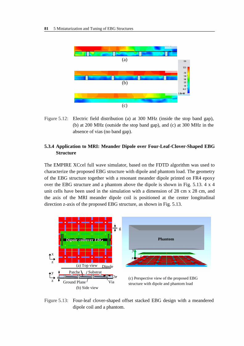
81 5 Miniaturization and Tuning of EBG Structures
Figure 5.12: Electric field distribution (a) at 300 MHz (inside the stop band gap), (b) at 200 MHz (outside the stop band gap), and (c) at 300 MHz in the absence of vias (no band gap).
5.3.4 Application to MRI: Meander Dipole over Four-Leaf-Clover-Shaped EBG Structure
The EMPIRE XCcel full wave simulator, based on the FDTD algorithm was used to characterize the proposed EBG structure with dipole and phantom load. The geometry of the EBG structure together with a resonant meander dipole printed on FR4 epoxy over the EBG structure and a phantom above the dipole is shown in Fig. 5.13. 4 x 4 unit cells have been used in the simulation with a dimension of 28 cm x 28 cm, and the axis of the MRI meander dipole coil is positioned at the center longitudinal direction z-axis of the proposed EBG structure, as shown in Fig. 5.13.
Figure 5.13: Four-leaf clover-shaped offset stacked EBG design with a meandered
dipole coil and a phantom.
(a)
(b)
(c)
Substrat
Dipole
g
2r t Via
Patche
(b) Side view Ground Plane
Dipole coil over EBG
(a) Top view z
x
z
y (c) Perspective view of the proposed EBG structure with dipole and phantom load
Phantom
y z x

5.3 Four-Leaf-Clover-Shaped EBG Structure 82
Figure 5.14: FDTD longitudinal (z-axis) distribution of magnetic over electric field ratio for meander dipole coil backed by the proposed EBG structure and a metallic ground plane of the same size.
The magnetic and electric field strengths inside a homogeneous phantom are recorded, and the simulation results compared to the case when the meander dipole coil is backed by a PEC ground plane of the same size.
The Ratio of Magnetic over Electric Field Inside the Phantom and Field of View (FOV) The performance of the original coil configuration based on a meander dipole coil over a PEC ground plane was compared to the performance of the design using the EBG structure as a ground plane. To compare both scenarios in a fair manner, the distribution of magnetic over electric field ratio is simulated 4 cm inside a homogeneous phantom (z = 30.5 cm, x = 15.4 cm, y = 10 cm, εr = 40, σ = 0.8 S/m) placed 2 cm above the coil. The entire height of the coil and the PEC or EBG structure is kept constant to 3.4 cm.
As can be seen from Fig. 5.14, the 25 cm stripline coil backed by the proposed EBG structure exhibits a stronger |H|/|E| than the original design when the RF coil was backed by a PEC. The improvement is due to the increase in |H|. The maximal improvement in this ratio reaches to 57%.
As shown in Fig. 5.14 and Fig. 5.15, the RF field of view is maximized when the dipole length is increased, from 25 cm to 35 cm. Thus the expensive scanner time in MRI could be minimized.
0 61 122 152.5 183 244 3050
0,005
0,01
0,015
0.02
0,025
0.03
Longitudinal distance (mm)
|H|/|
E| F
ield
ratio
Refference PEC4X4SlottedEBG-25cmRFcoil4X4SlottedEBG-35cmRFcoil4X4SlottedEBG-38cmRFcoil

83 5 Miniaturization and Tuning of EBG Structures
Figure 5.15: Magnetic field Hx distribution in air at 1 cm above (a) 35 cm RF dipole coil (b) 25 cm RF dipole coil. (FDTD simulation with EMPIRE).
5.4 Tuning of EBG Structures Tuning the resonant frequency is one of the challenges of EBG structures to be used in MRI, because it is essential to adjust the narrow resonance of the structure to the MRI coil resonant frequency. Furthermore, after fabrication it is difficult to tune an EBG structure by changing its dimensions, and it is difficult to be employed as a ground plane for other antennas or coils with different resonant frequencies, unless a multi-resonant EBG structure is designed. The design of EBG structures for MRI application requires the use of multilayers dielectric substrates and/or some complicated geometries to shift the resonance down to the MR system frequency, typically 298 MHz. Thus, the EBG structure designed for this application has a narrow bandwidth, and due to the effect of lossy substrates, material and fabrication tolerances, and the mismatch, if any, between the measurement and simulation results, it is essential to use an efficient technique to tune the resonant frequency of the EBG structure to the desired frequency.
To satisfy the aforementioned requirements, different methods have been proposed in the literature. The varactor diodes [55] can be used between the metallic patches to shift the resonant frequency, but the attendant biasing circuits to the non-magnetic diodes make the resultant EBG structure much more complicated than the conventional one. Furthermore, the RF pulse in MRI applications is of high power and the varactor diodes might be damaged. Another tuning technique is the method of micro-electro-mechanical system (MEMS) actuators [60] which particularly are used for EBG structures designed for high frequency applications.
In this section, two tuning techniques are proposed. The first one is based on inserting a mechanical adjustable air-gap layer at the bottom surface of the EBG structure, in the same way as those proposed for the patch antennas [60 - 62]. The second proposed tuning method is based on the coaxial cables. In this technique, coaxial cables are
(a) (b)
y x z
y x z
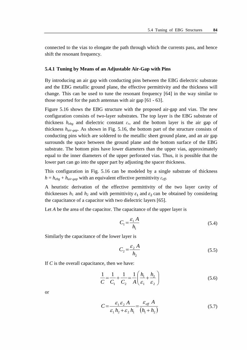
5.4 Tuning of EBG Structures 84
connected to the vias to elongate the path through which the currents pass, and hence shift the resonant frequency.
5.4.1 Tuning by Means of an Adjustable Air-Gap with Pins By introducing an air gap with conducting pins between the EBG dielectric substrate and the EBG metallic ground plane, the effective permittivity and the thickness will change. This can be used to tune the resonant frequency [64] in the way similar to those reported for the patch antennas with air gap [61 - 63].
Figure 5.16 shows the EBG structure with the proposed air-gap and vias. The new configuration consists of two-layer substrates. The top layer is the EBG substrate of thickness hebg and dielectric constant ɛr, and the bottom layer is the air gap of thickness hair-gap. As shown in Fig. 5.16, the bottom part of the structure consists of conducting pins which are soldered to the metallic sheet ground plane, and an air gap surrounds the space between the ground plane and the bottom surface of the EBG substrate. The bottom pins have lower diameters than the upper vias, approximately equal to the inner diameters of the upper perforated vias. Thus, it is possible that the lower part can go into the upper part by adjusting the spacer thickness.
This configuration in Fig. 5.16 can be modeled by a single substrate of thickness h = hebg + hair-gap with an equivalent effective permittivity ɛeff.
A heuristic derivation of the effective permittivity of the two layer cavity of thicknesses h1 and h2 and with permittivity 𝜀1 and 𝜀2 can be obtained by considering the capacitance of a capacitor with two dielectric layers [65].
Let A be the area of the capacitor. The capacitance of the upper layer is
1
11 h
AC ε=
(5.4)
Similarly the capacitance of the lower layer is
2
22 h
AC ε=
(5.5)
If C is the overall capacitance, then we have:
+=+=
2
2
1
1
21
1111εεhh
ACCC (5.6)
or
( )211221
21
hhA
hhAC eff
+=
+=
εεε
εε
(5.7)
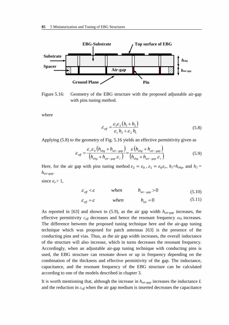
85 5 Miniaturization and Tuning of EBG Structures
hebgSubstrate
Spacer
Ground Plane
Air-gap
EBG-Substrate Top surface of EBG
hair-gap
Pin
Figure 5.16: Geometry of the EBG structure with the proposed adjustable air-gap
with pins tuning method.
where
( )1221
2121
hhhh
eff εεεεε
++
=
(5.8)
Applying (5.8) to the geometry of Fig. 5.16 yields an effective permittivity given as
( )( )
( )( )rgapairebg
gapairebg
rgapairebg
gapairebgreff hh
hhhh
hhε
εε
εεε
−
−
−
−
+
+=
+
+= 0
(5.9)
Here, for the air gap with pins tuning method 𝜀2 = 𝜀0 , 𝜀1 = 𝜀0𝜀𝑟, h1=hebg, and h2 = hair-gap.
since 𝜀𝑟> 1,
0>< −gapaireff hwhenεε
(5.10)
0== aireff hwhenεε
(5.11)
As reported in [63] and shown in (5.9), as the air gap width hair-gap increases, the effective permittivity ɛeff decreases and hence the resonant frequency ω0 increases. The difference between the proposed tuning technique here and the air-gap tuning technique which was proposed for patch antennas [63] is the presence of the conducting pins and vias. Thus, as the air gap width increases, the overall inductance of the structure will also increase, which in turns decreases the resonant frequency. Accordingly, when an adjustable air-gap tuning technique with conducting pins is used, the EBG structure can resonate down or up in frequency depending on the combination of the thickness and effective permittivity of the gap. The inductance, capacitance, and the resonant frequency of the EBG structure can be calculated according to one of the models described in chapter 3.
It is worth mentioning that, although the increase in hair-gap increases the inductance L and the reduction in ɛeff when the air gap medium is inserted decreases the capacitance

5.4 Tuning of EBG Structures 86
C, both changes have the advantage to increase the bandwidth although they exhibit opposite effects on the resonant frequency. Thereby, the dominant effect determines the value of the resonant frequency.
For demonstration in this section, the conventional mushroom-like EBG structure, presented in chapter 3, which has the following unit cell dimensions, is simulated
W = 0.097 λ300MHz, g = 0.001 λ300MHz, hebg = 0.014 λ300MHz, εr = 10.2, and r = 0.004 λ300MHz.
Underneath the EBG unit cell an adjustable air-gap with conducting pin is connected as the lower part of the unit cell. Periodic boundary conditions (PBCs) surround the four sides of the new unit cell to realize an infinite EBG structure with the tuning part.
The simulation result in Fig. 5.17 shows that, for the proposed air-gap tuning technique, when hair-gap increases from 0 to 1 mm the decrease in ɛeff, and hence in the capacitance C, has a dominant effect over the increase in the inductance L. Thus, the resonant frequency increases above ω0 of the original EBG structure. When the air-gap thickness increases greater than 1 mm, the overall inductance provided due to the increase in hair-gap becomes dominant over the reduction in the overall capacitance due to the decrease in ɛeff. When the thickness is 2 mm, as shown in Fig. 5.17, both effects cancel each other and any further increase in the air gap thickness will shift the resonance down in frequency.
This mechanical adjustable air-gap tuning technique with vias has advantages over the electronic one. It is less complicated and can be used for EBG structures regardless the geometry of patches, and it is more economical especially for large number of cells. The disadvantage of this method is the difficult adjustment of the air gap height and the reliable contacting of the pins inside the vias.
0 1 2 3 4 5 6260
270
280
290
300
310
Air-gap thickness (mm)
Res
onan
t fr
eque
ncy
(MH
z)
Figure 5.17: The resonant frequency versus the air gap thickness.
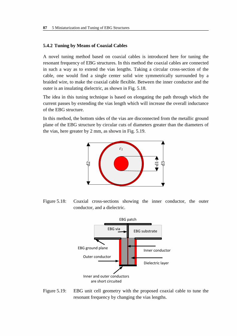
87 5 Miniaturization and Tuning of EBG Structures
5.4.2 Tuning by Means of Coaxial Cables A novel tuning method based on coaxial cables is introduced here for tuning the resonant frequency of EBG structures. In this method the coaxial cables are connected in such a way as to extend the vias lengths. Taking a circular cross-section of the cable, one would find a single center solid wire symmetrically surrounded by a braided wire, to make the coaxial cable flexible. Between the inner conductor and the outer is an insulating dielectric, as shown in Fig. 5.18.
The idea in this tuning technique is based on elongating the path through which the current passes by extending the vias length which will increase the overall inductance of the EBG structure.
In this method, the bottom sides of the vias are disconnected from the metallic ground plane of the EBG structure by circular cuts of diameters greater than the diameters of the vias, here greater by 2 mm, as shown in Fig. 5.19.
ɛ1
d1 d3d2
Outer conductorInner conductor
Dielectric layer
Inner and outer conductors are short circuited
EBG patch
EBG substrate
EBG ground plane
EBG via
Figure 5.18: Coaxial cross-sections showing the inner conductor, the outer conductor, and a dielectric.
Figure 5.19: EBG unit cell geometry with the proposed coaxial cable to tune the resonant frequency by changing the vias lengths.
5.4 Tuning of EBG Structures 88
The vias are reconnected again to the ground plane through the coaxial cables. The inner conductor of each coaxial cable is connected to the bottom side of the vias, and from the other end is short circuited to the coaxial outer conductor. Then, the coaxial outer conductor is reconnected to the ground plane, as shown in Fig. 5.19.
For the lossless assumed coaxial cable the inductance per unit length can be calculated as follows
𝐿′ =𝜇02𝜋
𝑙𝑛𝑑2𝑑1
(5.13)
Here d1 is the outer diameter of the inner conductor, while d2 is the inner diameter of the metallic shield. A unit cell based on the geometry of the four-leave-clover-shaped EBG structure with the unit cell dimensions reported in (5.3) is used. In this tuning technique a lossless conductors and any dielectric can be used. The short circuit connection between the inner and outer conductors at the rear side of the coaxial cable results in a total inductive effect. The full wave FEM-simulator HFSS is used with periodic boundary conditions (PBCs) put on four sides of the new unit cell with the proposed coaxial cable to realize an infinite EBG structure with the tuning parts.
It is worth mentioning that only when an oblique incident plane wave illuminates the EBG surface the vias will be excited. Thus, the current goes from the vias to the coaxial inner conductors, and because of the short circuited connection between the inner and outer conductors, the current is circulated again to the ground plane. This technique elongates the path through which the currents pass, from the vias to the ground plane, through the inner and outer conductors. Elongating the path of the current is actually similar to elongating the length of the vias; this will increase the total inductance of the EBG structure.
Figure 5.20 shows the TM reflection coefficients phase of the EBG structure when coaxial cables of different lengths are connected to the vias. It is observed that the increase in the length of the coaxial cable will increase the overall inductance and hence will shift the resonance down in frequency. A dual resonant behavior is observed as shown in Fig. 5.20, with lower and higher resonances compared to the resonant frequency (≈ 300 MHz) of the original EBG structure, i.e. without the coaxial cables.
The frequency separation between the upper and lower resonances for each reflection coefficient phase increases as the coaxial cable lengths increase. This can be seen in the divergence between the upper and lower resonant frequencies in Fig. 5.21.
The frequency ranges corresponding to the lower in-phase reflection coefficients of the proposed EBG structure with coaxial cables of different lengths may be useful for miniaturization rather than tuning: As the length of the coaxial cable increases the resonant frequency becomes much smaller than the MRI operating frequency.

89 5 Miniaturization and Tuning of EBG Structures
That means, the substrate permittivity and the patch width of the EBG structure can be redesigned and reduced to shift the resonance up to the MR system frequency, and this will compensate the reduction in bandwidth.
The frequency ranges corresponding to the upper in-phase reflection coefficients exhibit resonant frequencies higher but closer to the resonant frequency of the original EBG structure, i.e. without the coaxial cable. Therefore, these resonances could be useful for tuning.
100 150 200 250 300 350 400 450 500-180
-135
-90
-45
0
45
90
135
180
Frequency (MHz)
Ref
lect
ion
phas
es (
degr
ees)
Coaxial cable 5 mmCoaxial cable 10 mmCoaxial cable 15 mm
2 4 6 8 10 12 14 16 18 20 22 24180
220
260
300
340
380
Coaxial cable length (mm)
Upp
er a
nd lo
wer
reso
nant
freq
uenc
y (M
Hz)
Lower resonant frequencyUpper resonant frequency
Figure 5.20: Reflection coefficient phase of EBG structure with tuning coaxial cables of different lengths.
Figure 5.21: Upper and lower resonant frequencies of four-leaf clover-shaped EBG structure with coaxial cables of different lengths.

5.5 Conclusion 90
It is clearly shown in Fig. 5.21, when the length of the coaxial cable increases, the upper resonant frequency will decrease till it becomes closer to the designed resonant frequency of the original EBG structure. This enables the upward-tuning for the resonant frequency of the EBG structure by successively cutting the cables. By using this tuning method, it is also possible to redesign an EBG structure such that after inserting the coaxial cables the upper resonant frequencies crosses the MRI resonant frequency.
5.5 Conclusion In this chapter, different miniaturization techniques were proposed to design EBG structures for low frequency applications, in particular for working at the MRI operating frequency. These include the Hilbert and Peano curves inclusions of different orders, which increase the compactness of the wire in the same footprint size. Thus, the resonance is shifted down in frequency, however, with a considerable reduction in bandwidth. Another proposed miniaturization technique is based on magneto-dielectric substrate of permeability µr > 1 has efficient results on decreasing the resonant frequency and increasing the bandwidth. Due to the dependency of this method on substrates including an amount of ferrites, more measurements and investigations have to be taken to check its possibility to be used safely for ultra-high field MRI.
In this chapter, a multilayer four-leaf-clover-shaped EBG structure with a miniaturized electrical cell size of 7% of λ300MHz has been utilized. The analyzed EBG structure satisfied the AMC reflection coefficient property at the MRI operating frequency. The MRI RF dipole coil frequency was also located within the useful stop band gap through which the surface waves cease to propagate. The more the number of cells, the wider the stop band gap was. The MRI dipole coil backed by the proposed EBG structure exhibited stronger (by 57%) magnetic over electric field ratio than the original design using a conventional metallic ground plane for the coil. The longitudinal RF field of view (FOV) has been extended when the strip-line coil length was increased from 25 cm to 35 cm.
Different Tuning techniques were proposed to adjust the resonance of the EBG structure to the MRI resonant frequency, 300 MHz. A simple and economical mechanical adjustable air-gap layer with conducting pins was introduced. This technique is based on the effect of increasing the air gap thickness hair-gap on decreasing the effective permittivity ɛeff and the capacitance C and on increasing the inductance L. Both changes of C and L exhibit opposite effects on the resonant frequency, and the dominant effect determines the value of ω0. Coaxial cables proposed for tuning are connected to the vias to elongate the path through which the currents pass, and hence shift the resonance down in frequency. Dual resonant

91 5 Miniaturization and Tuning of EBG Structures
behavior is observed with upper and lower resonant frequencies decreasing with the increase in the length of the cable. It is observed that the lower resonant frequencies are much below the MRI operating frequency and hence useful for miniaturization whiles the upper resonant frequencies are closer to the MR system frequency and hence useful for tuning.
Chapter 6
Soft Surfaces
The surface wave and the anti-phase currents in the metallic conductor ground plane placed underneath the meander dipole transmit coil element for high field MRI, represent the main reasons for the reduction in RF magnetic flux density B1 above these coils (inside the phantom). The objective of this part of the thesis is to replace this metallic reflector with a special kind of anisotropic surface impedance, soft surface [66], with the aim of increasing the magnetic field.
In this chapter, a novel multilayer offset stacked polarization dependent EBG structure is proposed to work as a soft surface. The proposed structure is designed to exhibit very high surface impedance in the longitudinal direction, to behave like a perfect magnetic conductor (PMC) with tangential magnetic field near to zero in the transverse direction. The structure is also designed to exhibit very low surface impedance in the transversal direction, to approach the perfect electric conductor (PEC) ground plane behaviour with tangential electric field near to zero in the same direction. Thereby, the magnetic flux density inside the patient’s body is increased while the electric field and the specific energy absorption rate (SAR) are reduced. The increase in the magnetic field will further increase the signal-to-noise ratio and hence the contrast between the different tissues of the body and improve the resolution and quality of the scanned images by MRI machines.
These kinds of anisotropic surface impedances of the EBG structures may be designed to either stop the propagation of waves or to support a quasi-transverse electromagnetic TEM wave to propagate along the surface [66]. The former is called a soft surface, whereas the latter is a hard surface.
6.1 Definition of Soft and Hard Surfaces The names soft and hard surfaces were chosen by the analogy of acoustic soft and hard surfaces [67] (soft and hard to touch). In electromagnetics, a soft surface is a surface along which the power density flux (Poynting vector) is zero for any polarization. This means that no electromagnetic wave of any kind (including space waves and surface waves) will propagate along a soft surface. An electromagnetically hard surface is a surface along which only a TEM wave can propagate. The power density flux has a maximum value at the hard surface.
92

93 6 Soft Surfaces
The soft surface behaves like a perfect electric conductor (PEC) for TE polarization and as a perfect magnetic conductor (PMC) for the TM polarization; and vice-versa for the hard surface.
The soft and hard surfaces can be uniquely defined in terms of their anisotropic surface impedances, namely the longitudinal Zsl and the transversal Zst surface impedances, and as follows:
t
lsl H
EZ = (6.1)
l
tst H
EZ = (6.2)
where Hl and Ht are the longitudinal and transversal magnetic field on the surface respectively, El and Et are the corresponding components of the electric field.
The incident and scattered fields with respect to periodic structures are analyzed in the next section to derive a formula for the impedance and the reflection coefficient of these surfaces.
6.2 Impedance and Reflection Coefficient of Periodic Ground Planes 6.2.1 Incident and Scattered Fields in Terms of Floquet Harmonics Let us have a periodic structure with periodicity a and b in the x and y directions respectively, and as shown in Fig. 6.1. The plane wave incident on the periodic ground plane with angle of incidence 𝜃𝑖 , wavenumbers 𝑘𝑥,𝑘𝑦,𝑘𝑧 , free space wavenumber 𝑘0, and for the time convention 𝑒𝑗𝜔𝑡 can be written as follows [68]:
( ) zjkyjkxjkiz
iTE
iTM
i zyx eezEtElEE +++= ˆˆˆ
(6.3)
( ) zjkyjkxjkiz
iTM
iTE
i zyx eezHtHlHH +++= ˆˆˆ
(6.4)
Here, 𝑙 and �̂� represent the longitudinal and transversal unit vectors in the x-y plane, and the summation of the TMz and TEz fields represent the tangential field components in the x-y plane. For the TMz incident wave, the magnetic field is along the transverse direction while the electric field has longitudinal and z components. For the TEz wave, the magnetic field has longitudinal and z components while only the electric field is along the transverse direction.
The total tangential field in the free space above the periodic ground plane can be represented as the sum of incident and reflected waves, and can be found from the Floquet theorem as follows [21]:
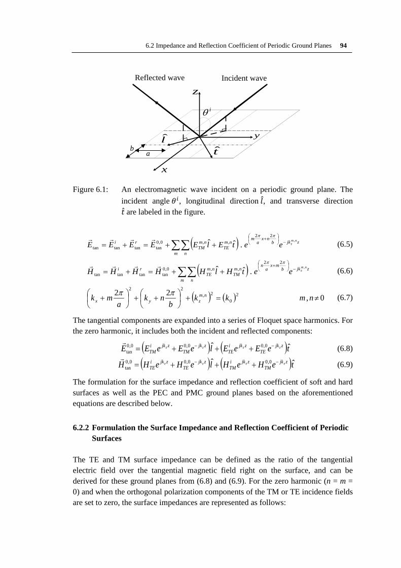
6.2 Impedance and Reflection Coefficient of Periodic Ground Planes 94
Reflected wave
x
y
z
l̂t̂
iθ
Incident wave
Figure 6.1:
An electromagnetic wave incident on a periodic ground plane. The incident angle 𝜃𝑖, longitudinal direction 𝑙, and transverse direction �̂� are labeled in the figure.
( ) zjkbnx
am
m n
nmTE
nmTM
ri nmzeetElEEEEE
,22
,,0,0tantantantan .ˆˆ −
+
∑∑ ++=+=ππ
(6.5)
( ) zjkbmx
an
m n
nmTM
nmTE
ri nmzeetHlHHHHH
,22
,,0,0tantantantan .ˆˆ −
+
∑∑ ++=+=ππ
(6.6)
( ) ( ) 0,22 20
2,22
≠=+
++
+ nmkk
bnk
amk nm
zyxππ
(6.7)
The tangential components are expanded into a series of Floquet space harmonics. For the zero harmonic, it includes both the incident and reflected components:
( ) ( )teEeEleEeEE zjkTE
zjkiTE
zjkTM
zjkiTM
zzzz ˆˆ 0,00,00,0tan
−− +++=
(6.8)
( ) ( )teHeHleHeHH zjkTM
zjkiTM
zjkTE
zjkiTE
zzzz ˆˆ 0,00,00,0tan
−− +++=
(6.9)
The formulation for the surface impedance and reflection coefficient of soft and hard surfaces as well as the PEC and PMC ground planes based on the aforementioned equations are described below.
6.2.2 Formulation the Surface Impedance and Reflection Coefficient of Periodic
Surfaces The TE and TM surface impedance can be defined as the ratio of the tangential electric field over the tangential magnetic field right on the surface, and can be derived for these ground planes from (6.8) and (6.9). For the zero harmonic (n = m = 0) and when the orthogonal polarization components of the TM or TE incidence fields are set to zero, the surface impedances are represented as follows:
a b
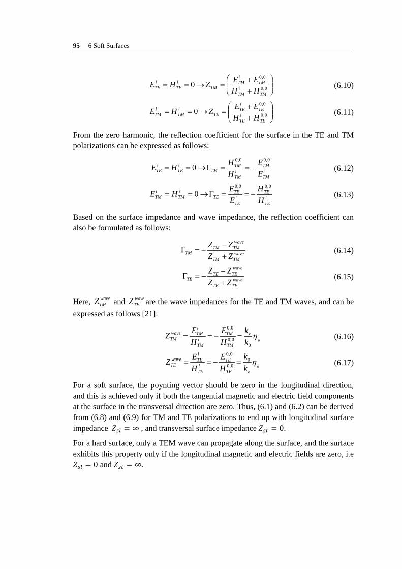
95 6 Soft Surfaces
++
=→== 0,0
0,0
0TM
iTM
TMiTM
TMiTE
iTE HH
EEZHE (6.10)
++
=→== 0,0
0,0
0TE
iTE
TEiTE
TEiTM
iTM HH
EEZHE (6.11)
From the zero harmonic, the reflection coefficient for the surface in the TE and TM polarizations can be expressed as follows:
iTM
TMiTM
TMTM
iTE
iTE E
EHHHE
0,00,0
0 −==Γ→== (6.12)
iTE
TEiTE
TETE
iTM
iTM H
HEEHE
0,00,0
0 −==Γ→== (6.13)
Based on the surface impedance and wave impedance, the reflection coefficient can also be formulated as follows:
waveTMTM
waveTMTM
TM ZZZZ
+−
−=Γ (6.14)
waveTETE
waveTETE
TE ZZZZ
+−
−=Γ (6.15)
Here, waveTMZ and wave
TEZ are the wave impedances for the TE and TM waves, and can be expressed as follows [21]:
0
00,0
0,0
ηkk
HE
HEZ z
TM
TMiTM
iTMwave
TM =−== (6.16)
0
00,0
0,0
ηzTE
TEiTE
iTEwave
TE kk
HE
HEZ =−== (6.17)
For a soft surface, the poynting vector should be zero in the longitudinal direction, and this is achieved only if both the tangential magnetic and electric field components at the surface in the transversal direction are zero. Thus, (6.1) and (6.2) can be derived from (6.8) and (6.9) for TM and TE polarizations to end up with longitudinal surface impedance 𝑍𝑠𝑙 = ∞ , and transversal surface impedance 𝑍𝑠𝑡 = 0.
For a hard surface, only a TEM wave can propagate along the surface, and the surface exhibits this property only if the longitudinal magnetic and electric fields are zero, i.e 𝑍𝑠𝑙 = 0 and 𝑍𝑠𝑡 = ∞.
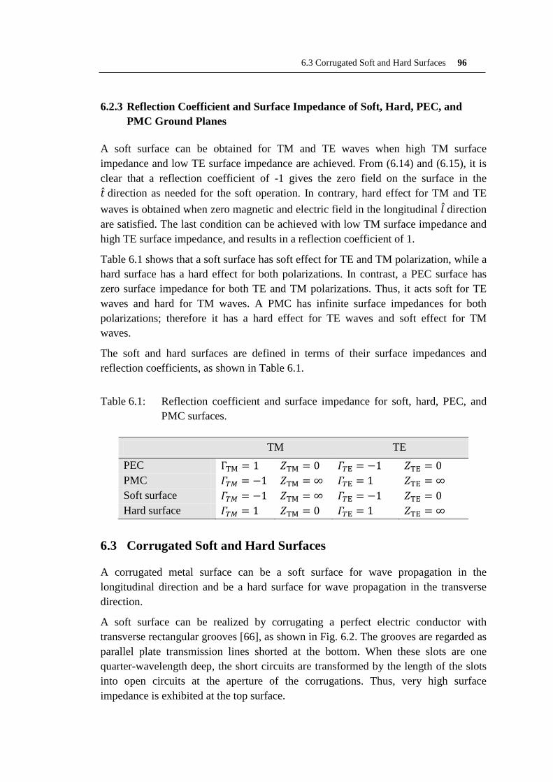
6.3 Corrugated Soft and Hard Surfaces 96
6.2.3 Reflection Coefficient and Surface Impedance of Soft, Hard, PEC, and PMC Ground Planes
A soft surface can be obtained for TM and TE waves when high TM surface impedance and low TE surface impedance are achieved. From (6.14) and (6.15), it is clear that a reflection coefficient of -1 gives the zero field on the surface in the �̂� direction as needed for the soft operation. In contrary, hard effect for TM and TE waves is obtained when zero magnetic and electric field in the longitudinal 𝑙 direction are satisfied. The last condition can be achieved with low TM surface impedance and high TE surface impedance, and results in a reflection coefficient of 1.
Table 6.1 shows that a soft surface has soft effect for TE and TM polarization, while a hard surface has a hard effect for both polarizations. In contrast, a PEC surface has zero surface impedance for both TE and TM polarizations. Thus, it acts soft for TE waves and hard for TM waves. A PMC has infinite surface impedances for both polarizations; therefore it has a hard effect for TE waves and soft effect for TM waves.
The soft and hard surfaces are defined in terms of their surface impedances and reflection coefficients, as shown in Table 6.1.
Table 6.1: Reflection coefficient and surface impedance for soft, hard, PEC, and
PMC surfaces.
TM TE PEC ΓTM = 1 𝑍TM = 0 𝛤𝑇E = −1 𝑍TE = 0 PMC 𝛤𝑇𝑀 = −1 𝑍TM = ∞ 𝛤𝑇E = 1 𝑍TE = ∞ Soft surface 𝛤𝑇𝑀 = −1 𝑍TM = ∞ 𝛤𝑇E = −1 𝑍TE = 0 Hard surface 𝛤𝑇𝑀 = 1 𝑍TM = 0 𝛤𝑇E = 1 𝑍TE = ∞
6.3 Corrugated Soft and Hard Surfaces A corrugated metal surface can be a soft surface for wave propagation in the longitudinal direction and be a hard surface for wave propagation in the transverse direction.
A soft surface can be realized by corrugating a perfect electric conductor with transverse rectangular grooves [66], as shown in Fig. 6.2. The grooves are regarded as parallel plate transmission lines shorted at the bottom. When these slots are one quarter-wavelength deep, the short circuits are transformed by the length of the slots into open circuits at the aperture of the corrugations. Thus, very high surface impedance is exhibited at the top surface.

97 6 Soft Surfaces
n̂t̂
l̂0=tE 0=tH
No propagation in the longitudinal direction
Transverse Corrugations
PEC
Figure 6.2: Realization of soft surface by metallic transversal corrugation
grooves.
n̂
t̂
l̂
0=tE0=tH
TEM waves propagate
in this direction
Longitudinal Corrugations
Figure 6.3: Realization of hard surface by metallic longitudinal corrugation
grooves.
This structure provides high impedance for electric fields polarized perpendicular to the grooves, thus the transversal component of the magnetic field is supressed.
The ideal conducting walls at the top faces of the corrugated surface provide low impedance for parallel electric fields, thus the tangential component of the electric field is zero. Therefore, the metallic transversal corrugated surface in Fig. 6.2 exhibits infinite surface impedance in the longitudinal direction and zero surface impedance in the transversal direction. These impedances make the transversal components of the magnetic and electric field to vanish. Therefore, the surface works ideally as a soft (Stop operation) with zero density of power flow in the longitudinal direction (assumed here as the direction of propagation). The more the number of corrugations per wavelength, the clearer the surface appears artificially soft.
Similarly, the hard surfaces can be realized by using corrugation grooves in the longitudinal direction (direction of propagation) as shown in Fig. 6.3. In hard surfaces only a TEM wave can propagate, and maximum density of power flow is in the longitudinal direction.

6.4 Realization and Characterization of Some Proposed Soft and Hard Surfaces 98
Soft surfa
ce direc
tion
Hard surface direction
PEC
PEC
Dielectric
Figure 6.4: Realization of soft and hard surfaces by a strip-loaded grounded
dielectric slab.
The hard operation property is achieved when the longitudinal magnetic and electric field components are zero. This is satisfied due to the infinite surface impedance in the transverse direction and zero surface impedance in the longitudinal direction.
Soft and hard surfaces can also be realized by filling the grooves of the corrugations with a dielectric or by using a strip-loaded coating technique [69], as seen in Fig. 6.4. A broad-band soft surface can theoretically be realized with alternate series of perfect electric and perfect magnetic transverse strips. The tangential components of the magnetic field vanish at the surface of a PMC, and the tangential components of the electric field are zero at the surface of a PEC.
The properties of soft surfaces are described in [70] with a “Stop” characteristic, where the surface wave propagation is suppressed. Similarly the hard operation is expressed as a “Go” operation because of the propagation of the TEM waves.
In the literature, the hard surface can be used for TEM waveguides and horn antennas, while the soft surface can be used to reduce coupling and provide isolation between arbitrarily polarized antennas located on the same ground plane [70].
In this work, we aim to realize a soft surface as a solution for the problem of the limited space available in MRI magnet bores.
6.4 Realization and Characterization of Some Proposed Soft and
Hard Surfaces In this section, some practical realizations for soft and hard surfaces are proposed for low frequency applications. The structures are mainly based on the gangbuster dipoles and slots frequency selective surfaces (FSSs) on grounded slabs.
The gangbuster FSS was first introduced as anisotropic surface in [17]. Gangbuster dipoles are proposed to realize metamaterial in [71] and to exhibit the behavior of an
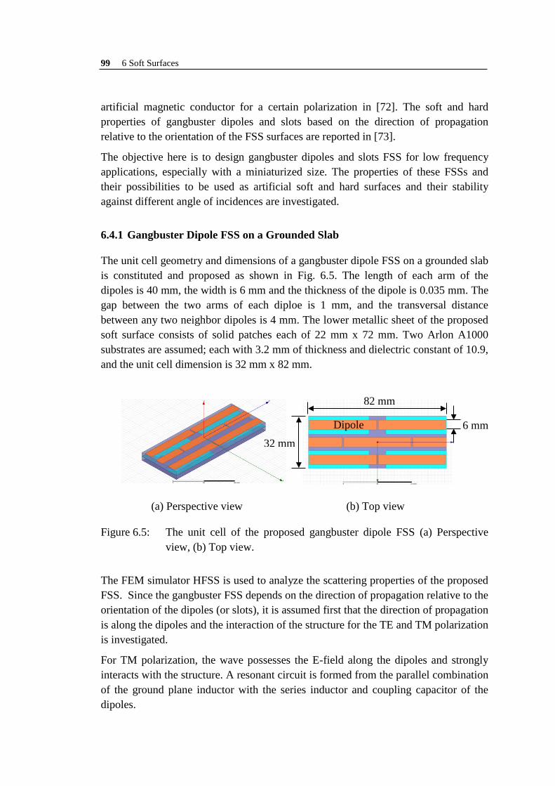
99 6 Soft Surfaces
artificial magnetic conductor for a certain polarization in [72]. The soft and hard properties of gangbuster dipoles and slots based on the direction of propagation relative to the orientation of the FSS surfaces are reported in [73].
The objective here is to design gangbuster dipoles and slots FSS for low frequency applications, especially with a miniaturized size. The properties of these FSSs and their possibilities to be used as artificial soft and hard surfaces and their stability against different angle of incidences are investigated.
6.4.1 Gangbuster Dipole FSS on a Grounded Slab The unit cell geometry and dimensions of a gangbuster dipole FSS on a grounded slab is constituted and proposed as shown in Fig. 6.5. The length of each arm of the dipoles is 40 mm, the width is 6 mm and the thickness of the dipole is 0.035 mm. The gap between the two arms of each diploe is 1 mm, and the transversal distance between any two neighbor dipoles is 4 mm. The lower metallic sheet of the proposed soft surface consists of solid patches each of 22 mm x 72 mm. Two Arlon A1000 substrates are assumed; each with 3.2 mm of thickness and dielectric constant of 10.9, and the unit cell dimension is 32 mm x 82 mm.
(a) Perspective view (b) Top view
Figure 6.5: The unit cell of the proposed gangbuster dipole FSS (a) Perspective view, (b) Top view.
The FEM simulator HFSS is used to analyze the scattering properties of the proposed FSS. Since the gangbuster FSS depends on the direction of propagation relative to the orientation of the dipoles (or slots), it is assumed first that the direction of propagation is along the dipoles and the interaction of the structure for the TE and TM polarization is investigated.
For TM polarization, the wave possesses the E-field along the dipoles and strongly interacts with the structure. A resonant circuit is formed from the parallel combination of the ground plane inductor with the series inductor and coupling capacitor of the dipoles.
6 mm
82 mm
32 mm
Dipole

6.4 Realization and Characterization of Some Proposed Soft and Hard Surfaces 100
Figure 6.6: The reflection phase versus the incidence angle theta and at different frequencies for a soft gangbuster dipole FSS.
Figure 6.7: The reflection phase versus the incidence angle theta and at different frequencies for a hard gangbuster dipole FSS.
For TM polarization the behavior of the proposed dipole FSS is the same as a PMC with very high surface impedance in the longitudinal direction, and this is true for a wide range of the incidence angles as can be concluded from the reflection coefficients shown in Fig.6.6.
This PMC behavior appears clearly around the resonant frequency (519 MHz) and with a frequency range (505 MHz - 533 MHz) over oblique incidence corresponding to the useful in-phase (±90o) reflection coefficient. For TE polarization, the thin dipoles are orthogonal to the E-field, and do not interact well with the FSS. Thus, the
-100 -80 -60 -40 -20 0 20 40 60 80 100-150
-100
-50
0
50
100
150
180200
Angle of Incidence, Theta
Ref
lect
ion
Pha
se (d
egre
es)
TM 505MHzTM 512MHzTM 519MHzTM 526MHzTM 533MHzTE 533MHzTE 526MHzTE 519MHz)TE 512MHzTE 505MHz
-100 -80 -60 -40 -20 0 20 40 60 80 100-200
-150
-100
-50
0
50
100
150
200
Angle of Incidence, Theta
Ref
lect
ion
Pha
se (d
egre
es)
TE 505MHzTE 512MHzTE 519MHzTE 526MHzTE 533MHzTM 505MHzTM 512MHzTM 519MHzTM 526MHzTM 533MHz
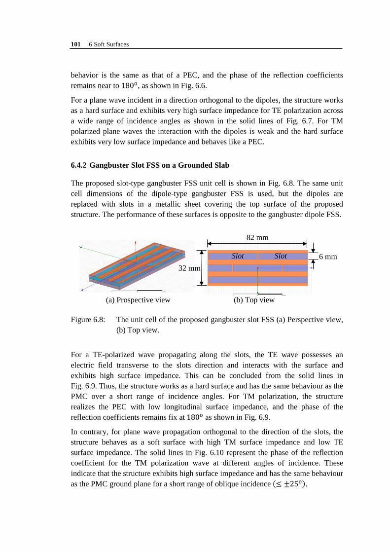
101 6 Soft Surfaces
behavior is the same as that of a PEC, and the phase of the reflection coefficients remains near to 180o, as shown in Fig. 6.6.
For a plane wave incident in a direction orthogonal to the dipoles, the structure works as a hard surface and exhibits very high surface impedance for TE polarization across a wide range of incidence angles as shown in the solid lines of Fig. 6.7. For TM polarized plane waves the interaction with the dipoles is weak and the hard surface exhibits very low surface impedance and behaves like a PEC.
6.4.2 Gangbuster Slot FSS on a Grounded Slab The proposed slot-type gangbuster FSS unit cell is shown in Fig. 6.8. The same unit cell dimensions of the dipole-type gangbuster FSS is used, but the dipoles are replaced with slots in a metallic sheet covering the top surface of the proposed structure. The performance of these surfaces is opposite to the gangbuster dipole FSS.
For a TE-polarized wave propagating along the slots, the TE wave possesses an electric field transverse to the slots direction and interacts with the surface and exhibits high surface impedance. This can be concluded from the solid lines in Fig. 6.9. Thus, the structure works as a hard surface and has the same behaviour as the PMC over a short range of incidence angles. For TM polarization, the structure realizes the PEC with low longitudinal surface impedance, and the phase of the reflection coefficients remains fix at 180o as shown in Fig. 6.9.
In contrary, for plane wave propagation orthogonal to the direction of the slots, the structure behaves as a soft surface with high TM surface impedance and low TE surface impedance. The solid lines in Fig. 6.10 represent the phase of the reflection coefficient for the TM polarization wave at different angles of incidence. These indicate that the structure exhibits high surface impedance and has the same behaviour as the PMC ground plane for a short range of oblique incidence (≤ ±25o).
Figure 6.8: The unit cell of the proposed gangbuster slot FSS (a) Perspective view, (b) Top view.
(a) Prospective view (b) Top view
6 mm
82 mm
32 mm Slot Slot

6.4 Realization and Characterization of Some Proposed Soft and Hard Surfaces 102
Figure 6.9: The reflection phase of a hard slot-type gangbuster surface for oblique incidence and with respect to different polarizations. Direction of propagation is along the slots.
The proposed slot-type gangbuster FSS resonates at 1095 MHz, which is beyond the scope of the MRI frequency. Thus, the slots must be longer to shift the resonance down in frequency. Furthermore, the useful high impedance surface property exhibited only over a short range of incidence angles.
For MRI applications, soft surfaces based on the dipole-type gangbuster FSS would be preferred over the slot FSS design. The dipole-type FSS provides a useful
-100 -80 -60 -40 -20 0 20 40 60 80 100-200
-150
-100
-50
0
50
100
150
200
Angle of Incidence, Theta
Ref
lect
ion
phas
e (d
egre
es)
TE 1091.5 MHzTE 1095 MHzTE 1098.5 MHzTM 1091.5 MHzTM 1095 MHz TM 1098.5 MHz
-100 80 60 40 20 0 20 40 60 80 100-100
-50
0
50
100
150
200
Angle of incidence, theta
Ref
lect
ion
phas
e (d
egre
es)
TM 1091.5MHzTM 1095MHzTM 1098.5MHzTE 1091.5MHzTE 1095MHzTE 1098.5MHz
Figure 6.10: The reflection phase of a soft slot-type gangbuster surface for oblique incidence and with respect to different polarizations. Direction of propagation is orthogonal to the slots.

103 6 Soft Surfaces
reflection phase property over a wide range of incidence angles and wide range of frequencies, and hence has higher bandwidth. Furthermore, the TM surface impedance of the dipole FSS is greater which implies lower resonances within the same size.
6.5 Application to MRI: The Proposed Soft Surface EBG 6.5.1 Materials and Methods In this chapter, a novel multilayer offset stacked polarization dependent EBG structure was designed with considerably reduced dimensions and fabricated to work as a soft surface ground plane for the meander dipole RF coil. Our proposed structure [74] possesses the unique properties of the EBG structures, i.e. gap characteristics, in-phase reflection coefficient and the stop band gap. The proposed structure consists of two arrays of metal patches diagonally offset from each other. The top layer consists of 4×3 patches each of 8% of λ300MHz in length and 3% of λ300MHz in width. These patches are connected to the metal backed dielectric substrate by vertical vias. The lower layer consists of solid patches and is floating.
The HFSS full wave simulator and the EMPIRE XCcel simulator are used to analyze and characterize the EBG structure. The geometry of the PEC and the proposed soft surface together with a resonant meander dipole printed on FR4 substrate (εr = 4.4, tan(δ) = 0.02) with dimensions 100 mm × 250 mm × 0.5 mm are shown in Fig. 6.11.
The physical dimensions of the proposed soft surface EBG unit cell are shown in Fig. 6.12 and described as follows:
Fig. 6.11: (a) Meander dipole backed by a PEC, (b) Meander dipole backed by 4x3 cells of the proposed EBG ground plane. Later each row of transverse patches was connected together.
(a) (b) z
y x
(a) (b)

6.5 Application to MRI: The Proposed Soft Surface EBG 104
W1
t1
Ground Plane
Upper patch
t2
Lower patch
ɛr
ɛr
L2 / 2
W2 / 2
L1
L1 = 0.08 λ300MHz, W1 = 0.03 λ300MHz, L2 = 0.072 λ300MHz, W2 = 0.022 λ300MHz , g = 0.002 λ300MHz, t1 = t2 = 0.0032 λ300MHz, r = 0.0025 λ300MHz, and ɛr = 10.9.
(6.18)
Here, λ300MHz is the free-space wavelength at 300 MHz, which is used as a reference length. L1 is the upper patch length, W1 is the upper patch width, L2 is the lower patch length, W2 is the lower patch width, g is the gap width, and t1 and t2 are the thicknesses of two Arlon AR-1000 substrates, with a relative dielectric constant of 10.9. The spacing between the two layers of patches was chosen to be 0.0032 λ300MHz due to the availability of laminates of 3.2 mm thickness. The two substrates are bonded together using a tape of 0.2 mm thickness and relative permittivity of 4.4.
The linear length of the meander dipole is λ300MHz/4. A 305 mm x 154 mm x 100 mm homogeneous phantom (εr = 40, σ = 0.8 S/m) is placed 2 cm above the coil to emulate the human body at the MRI frequency of 300 MHz. Two end capacitors are used at the end of the meanders to shift the resonance down in frequency to 300 MHz. The entire height of the coil and the PEC or soft surface is kept constant to 3.4 cm.
6.5.2 TE and TM Reflection Phase for the Proposed Soft Surface Fig. 6.13 shows the reflection coefficient phase of the proposed EBG structure when it works as a soft surface. For TM polarized waves illuminating the EBG surface, the E-field interacts strongly with the patches in the longitudinal direction. Thus, the surface exhibits high surface impedance and behaves like an artificial magnetic conductor (AMC). The longitudinal dimension of the patches is designed with the other parts of the structure to exhibit high longitudinal surface impedance with near zero tangential magnetic field. The solid lines in Fig. 6.13 show the insensitivity of the corresponding reflection coefficient phase for a wide range of oblique incidence of TM polarized fields, and for frequencies around the MRI resonant frequency f0 ± 1% of variation. In contrary, for TE polarized waves the E-field is orthogonal to the patches, i.e. in the transverse direction, and the soft surface exhibits low transverse surface impedance with near zero tangential electric field. Thus, the structure behaves like a PEC ground plane.
Figure 6.12: The proposed unit cell of the soft surface (a) Top view, (b) Side view.
(a) (b)

105 6 Soft Surfaces
Figure 6.13: Reflection phase of the proposed soft surface with TM- and TE- polarized plane wave at oblique incidence, and at different frequencies.
As can be seen from the solid lines of Fig. 6.13, the phase of the reflection coefficient of the proposed soft surface oscillates for the TM case around 0o with ±50o over a wide range of oblique incidence and for a range of operating frequencies. This less angle dependence behavior of the proposed soft surface ensures that the MRI operating frequency is always located inside the useful in-phase (±90o) reflection coefficient, where the fields are reflected in-phase. For TE polarization, the phase of the reflection coefficient remains at 180o , as shown by the dotted lines in Fig. 6.13.
6.5.3 Measurement and Simulation Results In this part, the properties of two fabricated soft surfaces are investigated by measurements. Then, numerical results are presented to investigate the magnetic and electric field strengths of the meander dipole when it is backed by a soft surface or a metallic ground plane of the same size.
Two soft surfaces were designed and fabricated as shown in Fig. 6.14. The larger structure has an overall size of 12.8 cm x 25 cm, and was designed initially with 4 x 3 unit cells of same dimensions as shown in (6.18). Our theoretical investigations proved that when the patches in each row are connected together to create one broad patch, this surface exhibits clearly the PEC ground plane behaviour in the transverse direction while keeping its PMC ground plane behaviour in the longitudinal direction. Thus, the proposed soft surface is fabricated so that it has 1x3 unit cells with 4x3 vias, as shown in Fig. 6.14a. The number and positions of vias are the same as in the previous design in Fig. 6.11b.
-100 -80 -60 -40 -20 0 20 40 60 80 100-100
-50
0
50
100
150
180200
Angle of incidence (degrees), Theta
Ref
lect
ion
phas
e (d
egre
es)
TM 297MHzTM 298MHzTM 299MHzTM 300MHzTM 301MHzTE 297MHzTE 298MHzTE 299MHzTE 300MHzTE 301MHz
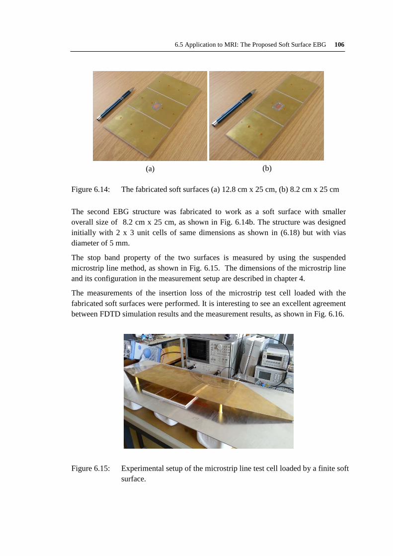
6.5 Application to MRI: The Proposed Soft Surface EBG 106
Figure 6.14: The fabricated soft surfaces (a) 12.8 cm x 25 cm, (b) 8.2 cm x 25 cm
The second EBG structure was fabricated to work as a soft surface with smaller overall size of 8.2 cm x 25 cm, as shown in Fig. 6.14b. The structure was designed initially with 2 x 3 unit cells of same dimensions as shown in (6.18) but with vias diameter of 5 mm.
The stop band property of the two surfaces is measured by using the suspended microstrip line method, as shown in Fig. 6.15. The dimensions of the microstrip line and its configuration in the measurement setup are described in chapter 4.
The measurements of the insertion loss of the microstrip test cell loaded with the fabricated soft surfaces were performed. It is interesting to see an excellent agreement between FDTD simulation results and the measurement results, as shown in Fig. 6.16.
Figure 6.15: Experimental setup of the microstrip line test cell loaded by a finite soft surface.
(a) (b)

107 6 Soft Surfaces
Figure 6.16: Simulated and measured transmission (S2,1) coefficient of the proposed 12.8 cm x 25 cm soft surface.
Figure 6.17: Measured transmission (S2,1) coefficient of the two soft surfaces.
The measured transmission coefficients show that the 12.8 cm x 25 cm structure exhibits a clear stop band gap centered at 297.6 MHz with deep S2,1 minimum of -21 dB. In contrast, the 8.2 cm x 25 cm soft surface exhibits a stop band gap at 296.5 MHz with a measured transmission coefficient minimum of -17 dB, as shown in Fig. 6.17. Thus, the two fabricated soft surfaces provide the surface wave suppression band gap property.
100 150 200 250 300 350 400 450 500-25
-20
-15
-10
-5
0
5
Frequency (MHz)
Mea
sure
d tra
nsm
isio
n c
oeffi
cien
t (dB
)
100 150 200 250 300 350 400 450 500-40
-30
-20
-10
05
Frequency (MHz)
Sim
ulat
ed tr
ansm
isio
nco
effic
ient
(dB
)
100 200 300 400 500-25
-20
-15
-10
-5
0
5
Frequency (MHz)
Mea
sure
d tra
nsm
isio
n co
effic
ient
, S21
(dB
)
Measured S21, 12.8 cm x 25 cm EBGMeasured S21, 8 cm x 25 cm EBG

6.5 Application to MRI: The Proposed Soft Surface EBG 108
Figure 6.18: Normalized magnetic field strength |H| [A/m/√W] 4 cm inside the
phantom.
One of the advantages of the fabricated soft surfaces over the previous proposed designs is that they provide the unique properties of EBG structures with miniaturized dimensions. Thereby, it is possible to use the proposed soft surfaces as ground planes for closely spaced multi-channel MRI RF coils.
With respect to the dominant problem of SAR in high-field MRI, the performance of the original coil configuration based on a meander dipole over a PEC ground plane is compared to the performance of the design using the soft surface as a ground plane. The comparison is done by simulating the distribution of magnetic and electric field 4 cm inside a homogeneous phantom. To compare in a fair manner, the same phantom and ground plane sizes are used, and their separation distance from the coil is kept constant, and all field values are normalized to the square root of the accepted power.
Figure 6.18 shows the normalized absolute magnetic field distribution 4 cm inside the phantom plotted along the longitudinal z-axis when the meander coil is backed by the proposed soft surface and when it is backed by a PEC of the same size. The result shows an increase by 20% in the magnetic field for the dipole backed by the proposed soft surface. This improvement comes from the high surface impedance property in the longitudinal direction of the proposed soft surface, which behaves as the PMC ground plane with in-phase reflection coefficient and a clear stop band gap property.
The normalized electric field distribution 4 cm inside the phantom for the dipole backed by the PEC and the proposed soft surface is also investigated. As can be seen from Fig. 6.19 the coil shows a reduction by 20% in the electric field when it is backed by the soft surface compared to the case when it is backed by the PEC ground plane.
0 61 122 152.5 183 244 3050
0.05
0.1
0.15
0.2
0.25
0.3
0.35
0.4
0.450.47
Longitudinal direction [mm]
Nor
mal
ized
| H
| [A
/m/s
qrt(P
acc)
]
Soft SurfacePEC
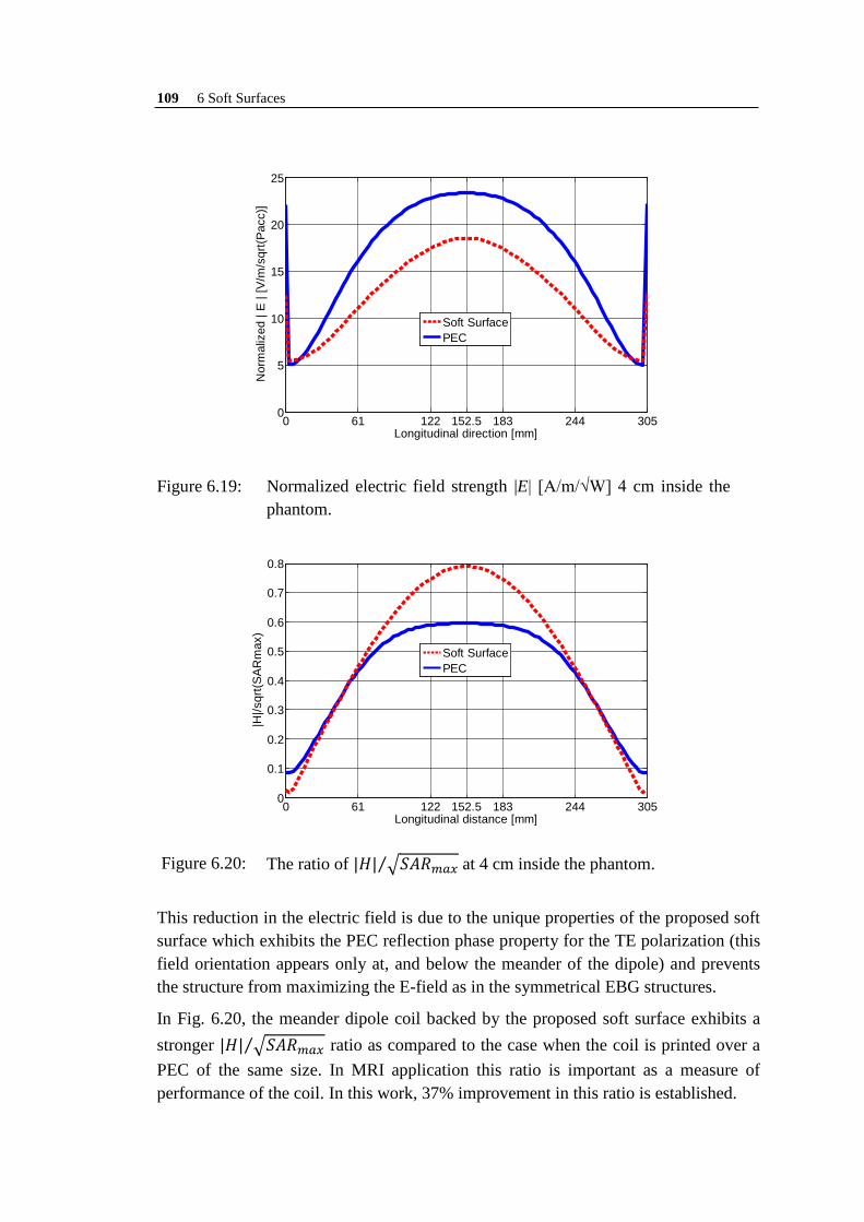
109 6 Soft Surfaces
Figure 6.19: Normalized electric field strength |E| [A/m/√W] 4 cm inside the
phantom.
Figure 6.20: The ratio of |𝐻| �𝑆𝐴𝑅𝑚𝑎𝑥⁄ at 4 cm inside the phantom.
This reduction in the electric field is due to the unique properties of the proposed soft surface which exhibits the PEC reflection phase property for the TE polarization (this field orientation appears only at, and below the meander of the dipole) and prevents the structure from maximizing the E-field as in the symmetrical EBG structures.
In Fig. 6.20, the meander dipole coil backed by the proposed soft surface exhibits a stronger |𝐻| �𝑆𝐴𝑅𝑚𝑎𝑥⁄ ratio as compared to the case when the coil is printed over a PEC of the same size. In MRI application this ratio is important as a measure of performance of the coil. In this work, 37% improvement in this ratio is established.
0 61 122 152.5 183 244 3050
5
10
15
20
25
Longitudinal direction [mm]
Nor
mal
ized
| E
| [V
/m/s
qrt(P
acc)
]
Soft SurfacePEC
0 61 122 152.5 183 244 3050
0.1
0.2
0.3
0.4
0.5
0.6
0.7
0.8
Longitudinal distance [mm]
|H|/s
qrt(S
AR
max
)
Soft SurfacePEC
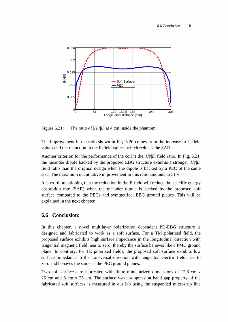
6.6 Conclusion 110
Figure 6.21: The ratio of |H|/|E| at 4 cm inside the phantom.
The improvement in the ratio shown in Fig. 6.20 comes from the increase in H-field values and the reduction in the E-field values, which reduces the SAR.
Another criterion for the performance of the coil is the |H|/|E| field ratio. In Fig. 6.21, the meander dipole backed by the proposed EBG structure exhibits a stronger |H|/|E| field ratio than the original design when the dipole is backed by a PEC of the same size. The maximum quantitative improvement in this ratio amounts to 51%.
It is worth mentioning that the reduction in the E-field will reduce the specific energy absorption rate (SAR) when the meander dipole is backed by the proposed soft surface compared to the PECs and symmetrical EBG ground planes. This will be explained in the next chapter.
6.6 Conclusion: In this chapter, a novel multilayer polarization dependent PD-EBG structure is designed and fabricated to work as a soft surface. For a TM polarized field, the proposed surface exhibits high surface impedance in the longitudinal direction with tangential magnetic field near to zero; thereby the surface behaves like a PMC ground plane. In contrary, for TE polarized fields, the proposed soft surface exhibits low surface impedance in the transversal direction with tangential electric field near to zero and behaves the same as the PEC ground planes.
Two soft surfaces are fabricated with finite miniaturized dimensions of 12.8 cm x 25 cm and 8 cm x 25 cm. The surface wave suppression band gap property of the fabricated soft surfaces is measured in our lab using the suspended microstrip line
0 61 122 152.5 183 244 3050
0.005
0.01
0.015
0.02
0,025
Longitudinal distance [mm]
|H|/|
E|
Soft SurfacePEC

111 6 Soft Surfaces
technique. The 12.8 cm x 25 cm soft surface exhibits a clear stop band gap at 297.6 MHz with deep transmission coefficient minimum of -21 dB. It is seen that also the 8.2 cm x 25 cm soft surface exhibits a stop band gap centred at 296.5 MHz with a measured transmission (S2,1) coefficient minimum of -17 dB.
The performance of the coil based on a meander dipole over the 12.8 cm x 25 cm soft surface is compared in a fair manner to the performance of the design using the metallic ground plane by simulating the distribution of magnetic and electric field 4 cm inside a homogeneous phantom. The FDTD results show the advantage of the proposed soft surface as it increases the magnetic field intensity (by 20%) inside the phantom while reduces the electric field (by 20%). Two ratios are used as a measure for the coil performance, namely, the H-field over the maximum SAR in one plane, and H-field over E-field ratio. The improvement in |𝐻| �𝑆𝐴𝑅𝑚𝑎𝑥⁄ reaches to 37%, and the maximum quantitative improvement in |H|/|E| field ratio amounts to 51%. It is observed that the reduction in the E-field may help to maintain the specific energy absorption rate SAR within the acceptable values in MRI operation.

Chapter 7
RF Safety and SAR
In this chapter the Specific Absorption Rate (SAR) values inside the phantom in the case when a coil is backed by a PEC and when it is backed by an EBG structure are investigated and compared. Although the SAR topic is beyond the scope of this work two novel techniques have been introduced as solutions to reduce the SAR values inside the load for MRI applications. These include the method of using dielectric overlays over the meander coil and the method of using polarization dependent EBG structures, in particular soft surfaces. These techniques have been presented partially in our research [74, 75].
7.1 RF Safety and Guidelines RF exposure is measured as either an increase in tissue temperature or as the Specific Absorption Rate (SAR). The SAR is an appropriate parameter used as a measure for determining the rate at which electromagnetic energy is absorbed by biological tissue mass when exposed to a radio frequency (RF) source.
The time varying magnetic flux induces electric fields 𝐸�⃗ which cause eddy currents of density 𝐽 = 𝜎𝐸�⃗ inside conductive tissue, such as the human body. This amounts to electric power losses P which are proportional to the B1 field and Larmor frequency ω squared, and can create heat in the human body. Since tissue temperatures are normally not accessible during MRI examinations, the RF power absorbed per kilogram of tissue (SAR) is used to set safety limits for MRI. The local SAR within the exposed tissue of density ρ can be expressed as
221
22
221 ω
ρσρσ
ρρBJE
ddPSAR ∝===
(7.1)
Where ρ is the mass density of the tissue in Kg, and σ is the electric conductivity in S/m. From (7.1) it is clear that doubling the magnetic field or pulse flip angle will quadruple the SAR, and thus SAR introduce major limitations for ultra-high field MRI.
If a numerical technique is used in order to estimate the electric field, a discretized simulation domain is used and the averaged SAR can be computed as follows [76]
112

113 7 RF Safety and SAR
( ) ∑∑∈∈
∆∆=)()(
2 /2/rmVi
irmVi
ii VVESAR ρσ (7.2)
Here rm is the reference averaging mass and V (rm) is a volume containing rm. It is found that the shape of the volume containing the reference averaging mass does affect the FDTD calculations of SAR values. The distribution of electric field inside the tissues varies from point to another, and the use of different volumes could generate differences in the evaluated SAR. To compare in a fair manner a homogenous phantom of the same volume is used for all scenarios in this chapter.
In order to protect the patient from rapid temperature rise and local tissue damage during an MRI examination, the SAR limits specified in the RF safety guidelines [77 - 79], must not be exceeded. In these guidelines the specific absorption rate (SAR) averaged over a certain reference tissue mass, is usually one gram (1 g), or 10 g or the whole body mass.
MR safety standards define limits for the whole body SAR and for the peak spatial average SAR (hot spots or local maxima) for various operational modes of the MR scanner. According to the IEC standard 60601-2-33 21 [79] for the occupational exposure of RF field, the SAR may not exceed 4 W/kg for body and 3.2 W/kg for head imaging. The spatial peak SAR averaged over any 10 g of tissue (defined as a tissue volume in the shape of a cube) shall not exceeding 10 W/kg for head and trunk and 20 W/kg for the extremities.
It is essential that any pulse sequence must not rise the body temperature by more than 1o Celsius which result from the prolonging exposure to an input SAR of 4 W/kg [78]. Especially for high-field MR systems and at higher frequencies, the SAR may depend strongly on the local tissue distribution and the localized SAR is often the most critical aspect concerning RF safety [80].
7.2 SAR for RF Coil Backed by a PEC and EBG Ground Planes In this section, the whole body SAR and the 10g-based local maximum SAR inside a homogeneous phantom are simulated and compared for the cases when the RF coil is backed by our proposed EBG structure in [43], as introduced in chapter 4, and a metallic PEC ground plane. To compare in a fair manner the same RF coil, phantom, and ground plane size are used. The simulations are performed with the FDTD simulator EMPIRE XCcel.
A resonant meandered dipole is used as RF-transmit element coil for 7 Tesla MRI. It is mounted on FR4 epoxy substrate of 0.5 mm thickness and relative permittivity of 4.4. The entire height between the coil and each of the PEC and EBG ground planes is kept fixed.
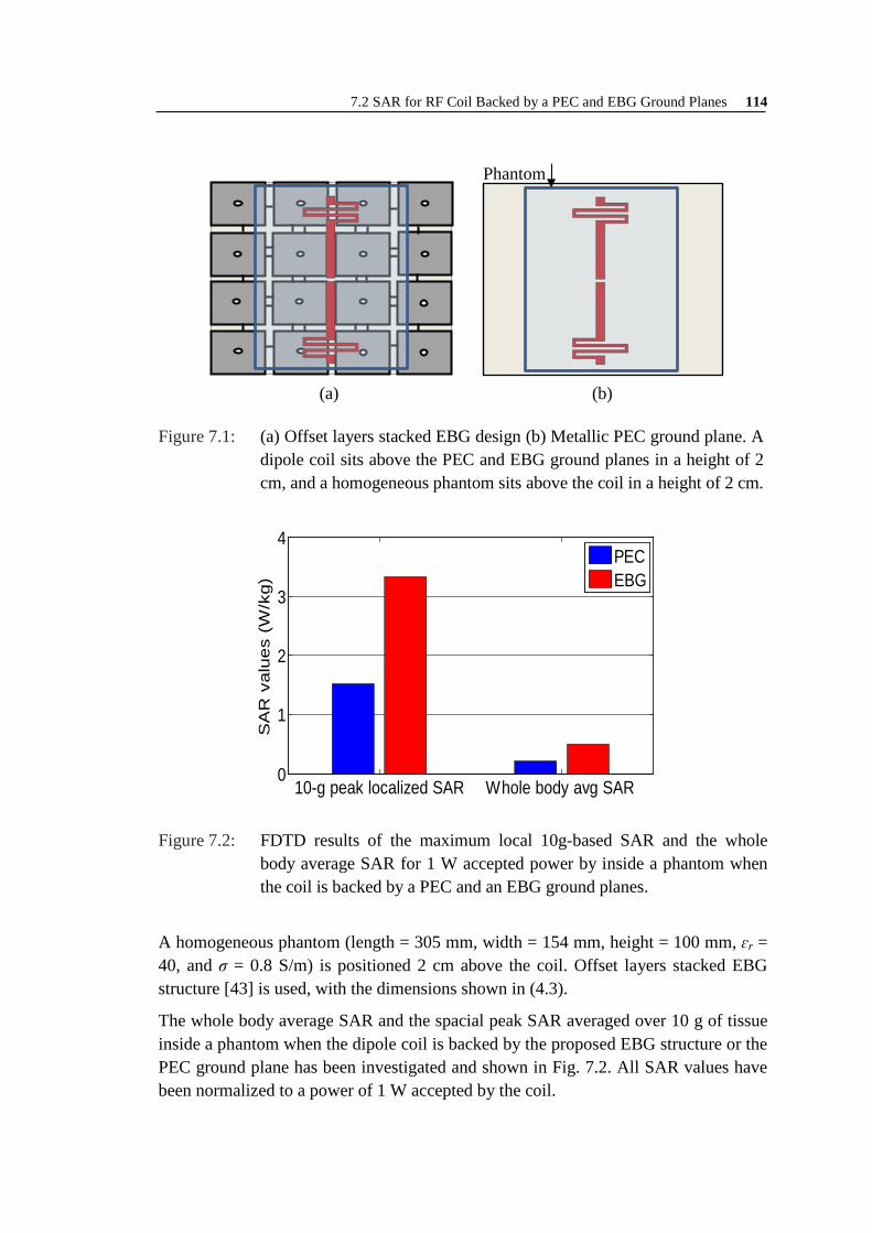
7.2 SAR for RF Coil Backed by a PEC and EBG Ground Planes 114
Figure 7.2: FDTD results of the maximum local 10g-based SAR and the whole body average SAR for 1 W accepted power by inside a phantom when the coil is backed by a PEC and an EBG ground planes.
A homogeneous phantom (length = 305 mm, width = 154 mm, height = 100 mm, ɛr = 40, and σ = 0.8 S/m) is positioned 2 cm above the coil. Offset layers stacked EBG structure [43] is used, with the dimensions shown in (4.3).
The whole body average SAR and the spacial peak SAR averaged over 10 g of tissue inside a phantom when the dipole coil is backed by the proposed EBG structure or the PEC ground plane has been investigated and shown in Fig. 7.2. All SAR values have been normalized to a power of 1 W accepted by the coil.
10-g peak localized SAR Whole body avg SAR 0
1
2
3
4
SA
R v
alue
s (W
/kg)
PECEBG
Figure 7.1: (a) Offset layers stacked EBG design (b) Metallic PEC ground plane. A dipole coil sits above the PEC and EBG ground planes in a height of 2 cm, and a homogeneous phantom sits above the coil in a height of 2 cm.
(a) (b)
Phantom

115 7 RF Safety and SAR
As can be seen from Fig. 7.2 when the coil is backed by the proposed EBG structure, the normalized 10g-based local maxima SAR was 3.334 mW/g, while this value reached to 1.518 mW/g in the case when the coil was backed by the PEC ground plane. The peak localized 10g-based SAR is found at the bottom surface of the phantom.
The difference in these SAR values is mainly due to the in-phase reflection and surface waves suppression properties exhibited by the EBG structure versus the PEC ground plane which increases both the electric field as well as the magnetic field. According to the aforementioned SAR guidelines, the SAR values for both the PEC and EBG ground planes in this example are still below the SAR restrictions [6]. The percentage of increase in the √SAR for the EBG structure case to the √SAR for the metallic ground plane case was about 48% and this corresponds to the percentage of improvement in the B1 efficiency, as described in chapter 4.
7.3 SAR Reduction Techniques In this section, two effective approaches based on dielectric overlay and polarization dependent EBG structure are proposed to reduce the specific absorption rate (SAR) values of the meander dipole RF coil for 7 Tesla MRI.
7.3.1 The Reduction of SAR Using Dielectric Overlay In this approach, the meander dipole coil is used with two dielectric substrates mounted on top of the folded arms of the coil to reduce the electric field as well as the SAR value which is a limiting factor for increasing the performance of 7 Tesla MRI RF coils. This work has been repeated with different permittivities.
Materials and Methods
First, the initial meander dipole RF coil geometry, described in chapter 2, has been utilized with a quarter wavelength element printed on FR4 substrate ( rε = 4.4, )tan(δ = 0.02) of 0.5 mm thickness, and separated by 20 mm of air from a metallic ground plane. The dimensions of this printed circuit board (PCB) are 250 mm in length and 100 mm in width. The effect of loading is considered by using a homogeneous phantom 20 mm above the coil, with a dimension of 305 mm x 154 mm x 100 mm. Its material properties (permittivity of 40 and 0.8 S/m conductivity) are used to model the human body when it is exposed to electromagnetic fields at 300 MHz. For the two proposed approaches, two capacitors are connected from the end of the meander arms to the ground plane to tune the resonant frequency to 300 MHz and through which current flows into the ground plane (hence we have a loop).
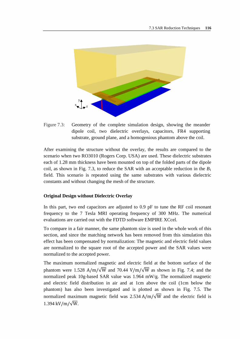
7.3 SAR Reduction Techniques 116
After examining the structure without the overlay, the results are compared to the scenario when two RO3010 (Rogers Corp. USA) are used. These dielectric substrates each of 1.28 mm thickness have been mounted on top of the folded parts of the dipole coil, as shown in Fig. 7.3, to reduce the SAR with an acceptable reduction in the B1 field. This scenario is repeated using the same substrates with various dielectric constants and without changing the mesh of the structure.
Original Design without Dielectric Overlay In this part, two end capacitors are adjusted to 0.9 pF to tune the RF coil resonant frequency to the 7 Tesla MRI operating frequency of 300 MHz. The numerical evaluations are carried out with the FDTD software EMPIRE XCcel.
To compare in a fair manner, the same phantom size is used in the whole work of this section, and since the matching network has been removed from this simulation this effect has been compensated by normalization: The magnetic and electric field values are normalized to the square root of the accepted power and the SAR values were normalized to the accepted power.
The maximum normalized magnetic and electric field at the bottom surface of the phantom were 1.528 A/m/√W and 70.44 V/m/√W as shown in Fig. 7.4; and the normalized peak 10g-based SAR value was 1.964 mW/g. The normalized magnetic and electric field distribution in air and at 1cm above the coil (1cm below the phantom) has also been investigated and is plotted as shown in Fig. 7.5. The normalized maximum magnetic field was 2.534 A/m/√W and the electric field is 1.394 kV/m/√W.
Figure 7.3: Geometry of the complete simulation design, showing the meander dipole coil, two dielectric overlays, capacitors, FR4 supporting substrate, ground plane, and a homogenious phantom above the coil.
z
y x

117 7 RF Safety and SAR
Dielectric Overlay with Various Permittivities In this scenario [75], first, two Rogers RO3010 substrates of the same dimensions (27 mm x 100 mm x 1.28 mm) are mounted only on top of the meander arms of the dipole coil, as shown in Fig. 7.3. The two caps Cend values are reduced from 0.9 pF to 0.5 pF to adjust the resonance frequency to 300 MHz as shown in the solid line of Fig. 7.6, and then the magnetic, electric and SAR values have been recorded. It is found that due to the dielectric overlay and the little caps used in this scenario, the normalized electric field at 1cm below the phantom is reduced.
Figure 7.4: (a) Magnetic field distribution at the bottom surface of a phantom, 2 cm above the coil. (b) Electric field distribution at the bottom surface of a phantom, 2 cm above the coil. Field values are normalized to �𝑃𝑎𝑐𝑐.
Figure 7.5: (a) Magnetic field distribution in air, 1cm above the coil (1 cm below the phantom), (b) Electric field distribution in air, 1 cm above the coil (1 cm below the phantom). Field values are normalized to �𝑃𝑎𝑐𝑐.
(a) (b)
(a) (b)
z
y x

7.3 SAR Reduction Techniques 118
The reduction in electric field was from 1.394 kV/m/√W in the original design to 1.286 kV/m/√W. This advantage helps us to avoid skin burn in ultra-high field MRI.
In this work, the effect of using the same dielectric overlay with various dielectric constants has also been investigated, while the same structure has been maintained and the mesh does not change. Fig. 7.6 shows the effect of decreasing the permittivity of the dielectric substrates on shifting up the resonance frequency.
To ensure that all comparisons of the different scenarios are taken in a fair manner, changing the permittivity of the dielectric substrates in each case was accompanied by tuning the end caps Cend to the optimum value which shifts the resonance frequency down again to the MRI operating frequency.
Fig. 7.7 shows the longitudinal normalized magnetic and electric field distribution, along the centre of the strip-line axis, and at the bottom surface of a phantom, 2 cm above the coil. From this Figure, it is clear that the maximum values of magnetic and electric field in the original design (solid lines) and with overlays of different dielectric constants (dashed lines) are found at bottom centre of the phantom. The principle distribution in Fig. 7.7 does not change, only the magnitude decreases with increasing ɛr.
125 200 300 400 500 600-7
-6
-5
-4
-3
-2
-1
0
Frequency (MHz)
Scat
terin
g Pa
ram
eter
S11
(dB)
RO3010EPSR 6EPSR 2
Figure 7.6: S1,1 parameters when substrates of various dielectric constants are used, and all with Cend = 0.5 pF.
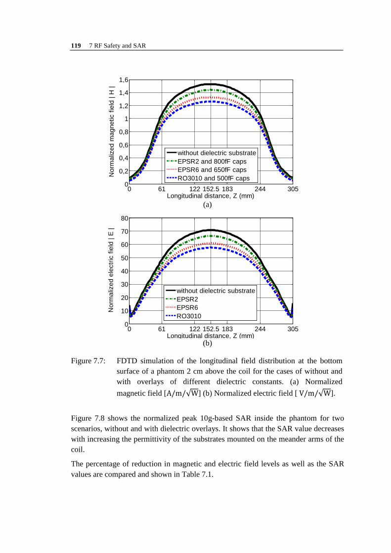
119 7 RF Safety and SAR
(a)
(b)
Figure 7.8 shows the normalized peak 10g-based SAR inside the phantom for two scenarios, without and with dielectric overlays. It shows that the SAR value decreases with increasing the permittivity of the substrates mounted on the meander arms of the coil.
The percentage of reduction in magnetic and electric field levels as well as the SAR values are compared and shown in Table 7.1.
0 61 122 152.5 183 244 3050
0,2
0,4
0,6
0,8
1
1,2
1,4
1,6
Longitudinal distance, Z (mm)
Nor
mal
ized
mag
netic
fiel
d | H
|
without dielectric substrateEPSR2 and 800fF capsEPSR6 and 650fF capsRO3010 and 500fF caps
0 61 122 152.5 183 244 3050
10
20
30
40
50
60
70
80
Longitudinal distance, Z (mm)
Nor
mal
ized
ele
ctric
fiel
d | E
|
without dielectric substrateEPSR2EPSR6RO3010
Figure 7.7: FDTD simulation of the longitudinal field distribution at the bottom surface of a phantom 2 cm above the coil for the cases of without and with overlays of different dielectric constants. (a) Normalized magnetic field [A/m/√W] (b) Normalized electric field [ V/m/√W].
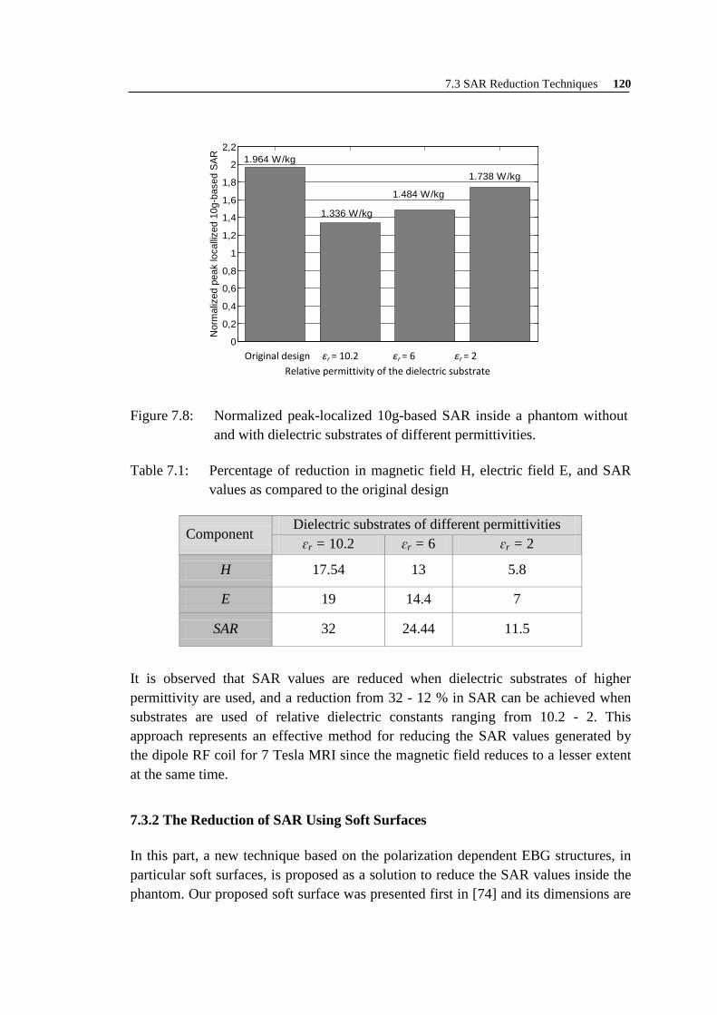
7.3 SAR Reduction Techniques 120
Table 7.1: Percentage of reduction in magnetic field H, electric field E, and SAR
values as compared to the original design It is observed that SAR values are reduced when dielectric substrates of higher permittivity are used, and a reduction from 32 - 12 % in SAR can be achieved when substrates are used of relative dielectric constants ranging from 10.2 - 2. This approach represents an effective method for reducing the SAR values generated by the dipole RF coil for 7 Tesla MRI since the magnetic field reduces to a lesser extent at the same time.
7.3.2 The Reduction of SAR Using Soft Surfaces In this part, a new technique based on the polarization dependent EBG structures, in particular soft surfaces, is proposed as a solution to reduce the SAR values inside the phantom. Our proposed soft surface was presented first in [74] and its dimensions are
Figure 7.8: Normalized peak-localized 10g-based SAR inside a phantom without and with dielectric substrates of different permittivities.
Component Dielectric substrates of different permittivities ɛr = 10.2 ɛr = 6 ɛr = 2
H 17.54 13 5.8
E 19 14.4 7
SAR 32 24.44 11.5
Original design RO3010 EPSR 6 EPSR 20
0,2
0,4
0,6
0,8
1
1,2
1,4
1,6
1,8
2
2,2
Relative permitivity of the dielectric substrate
Nor
mal
ized
pea
k lo
calliz
ed 1
0g-b
ased
SAR 1.964 W/kg
1.336 W/kg
1.484 W/kg
1.738 W/kg
Original design ɛr = 10.2 ɛr = 6 ɛr = 2 Relative permittivity of the dielectric substrate
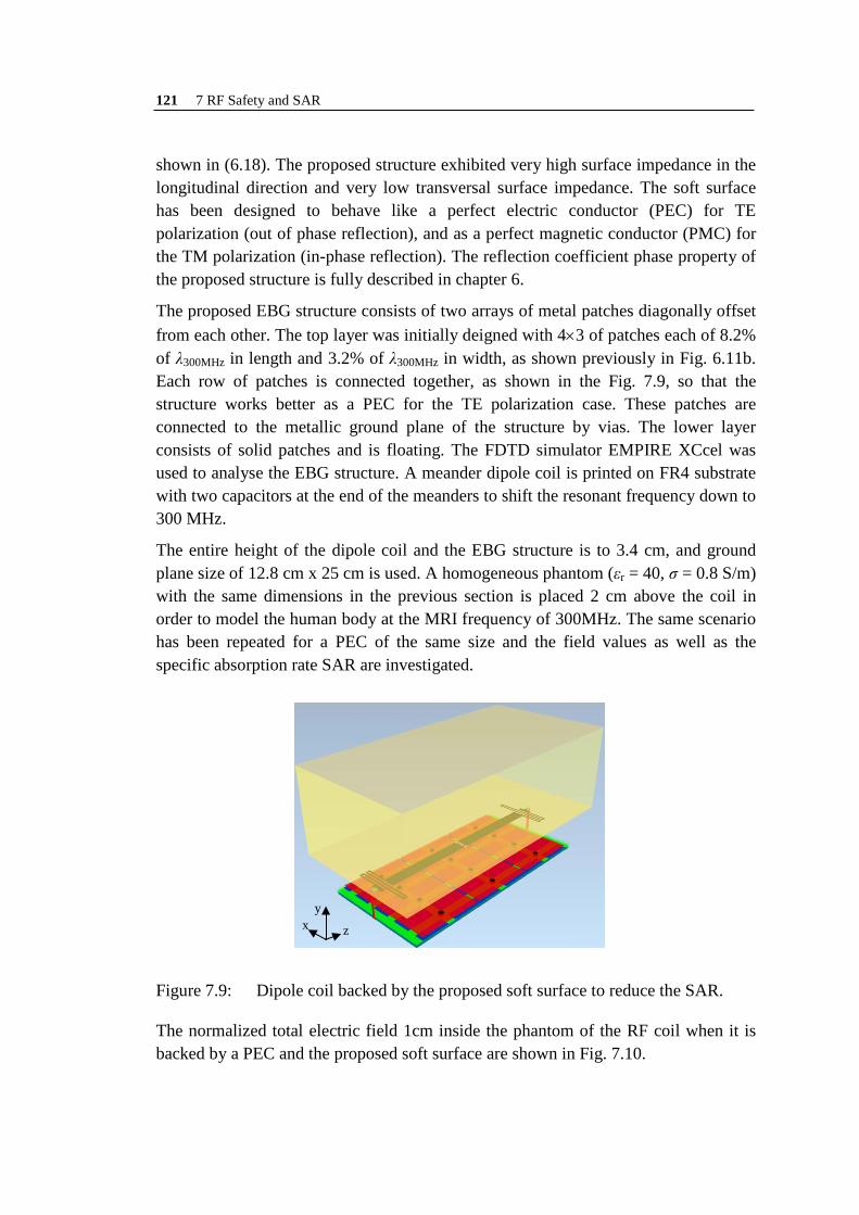
121 7 RF Safety and SAR
shown in (6.18). The proposed structure exhibited very high surface impedance in the longitudinal direction and very low transversal surface impedance. The soft surface has been designed to behave like a perfect electric conductor (PEC) for TE polarization (out of phase reflection), and as a perfect magnetic conductor (PMC) for the TM polarization (in-phase reflection). The reflection coefficient phase property of the proposed structure is fully described in chapter 6.
The proposed EBG structure consists of two arrays of metal patches diagonally offset from each other. The top layer was initially deigned with 4×3 of patches each of 8.2% of λ300MHz in length and 3.2% of λ300MHz in width, as shown previously in Fig. 6.11b. Each row of patches is connected together, as shown in the Fig. 7.9, so that the structure works better as a PEC for the TE polarization case. These patches are connected to the metallic ground plane of the structure by vias. The lower layer consists of solid patches and is floating. The FDTD simulator EMPIRE XCcel was used to analyse the EBG structure. A meander dipole coil is printed on FR4 substrate with two capacitors at the end of the meanders to shift the resonant frequency down to 300 MHz.
The entire height of the dipole coil and the EBG structure is to 3.4 cm, and ground plane size of 12.8 cm x 25 cm is used. A homogeneous phantom (εr = 40, σ = 0.8 S/m) with the same dimensions in the previous section is placed 2 cm above the coil in order to model the human body at the MRI frequency of 300MHz. The same scenario has been repeated for a PEC of the same size and the field values as well as the specific absorption rate SAR are investigated.
The normalized total electric field 1cm inside the phantom of the RF coil when it is backed by a PEC and the proposed soft surface are shown in Fig. 7.10.
Figure 7.9: Dipole coil backed by the proposed soft surface to reduce the SAR.
z
y x

7.3 SAR Reduction Techniques 122
Figure 7.11: The 10g-based and 1g-based SAR 1 cm inside a homogeneous
phantom sits 2 cm above a meander dipole coil backed by the proposed soft surface and a PEC ground plane of the same size. All SAR values have been normalized to an accepted power of 1 W.
Figure 7.10 shows that the normalized total electric field for RF coil backed by a PEC 1cm inside the phantom is 54 V/m/√W compared to 40 V/m/√W for the case when the RF coil backed by the proposed surface. This reduction is mainly due to the phase
0 152.5 3050
10
20
30
40
50
60
Longitudinal distance, z (mm)
Nor
mal
ized
ele
ctric
fiel
d (V
/m)
Soft SurfacePEC
Figure 7.10: The longitudinal total electric field strength 1 cm inside the phantom for a meander dipole coil backed by (a) Perfect electric conductor PEC, and (b) The proposed soft surface – EBG ground plane. Field values are normalized to �𝑃𝑎𝑐𝑐.
SAR_10g SAR_1g0
0.5
1
1.5
2
2.5
3
3.5
4
10g and 1g based SAR
Norm
alize
d pe
ak lo
caliz
ed S
AR v
alue
s
PECEBG
1.478 W/kg
2.612 W/kg
3.45 W/kg
1.91 W/kg

123 7 RF Safety and SAR
property of the soft surface which has been designed to reflect the fields out of phase for TE polarization and in-phase for the TM polarization.
Due this reduction in the electric field inside the phantom, the peak localized specific absorption rate SAR values (hot spots), which is a dominant restriction for MRI of high field strengths, is also reduced. Figure 7.11 shows the maximum 10g-based and 1g-based SAR values inside the phantom when the RF coil is backed by the proposed soft surface and a PEC ground plane of the same size. When this polarization dependent EBG structure is used as a ground plane for the RF coil in MRI, a significant reduction (by around 43%) in the local SAR is observed, as shown in Fig. 7.11. The 10g-SAR and 1g-SAR values for the PEC and the proposed EBG ground planes are reduced from 2.612 W/kg to 1.478 W/kg and from 3.45 W/kg to 1.91 W/kg respectively.
7.4 Conclusion
In this chapter, two techniques are proposed to reduce the specific absorption rate SAR values of the meander dipole RF coil for 7 Tesla MRI. The first approach is based on a dielectric overlay mounted on the folded arms of the meander dipole coil. It is observed that SAR values are reduced when dielectric substrates of higher permittivity are used, and a reduction from (12 - 32) % of SAR values could be achieved when substrates are used with dielectric constants of 2 - 10.2.
The second novel approach is based on polarization dependent EBG structures, here we use soft surfaces. These surfaces have the artificial magnetic property (with ±90o reflection phase) and reflect the fields in-phase for the TM polarization, and exhibit the perfect electric conductor property (around 1800 degree reflection phase) to reflect the fields out of phase for the TE polarization. The RF coil backed by the proposed EBG structure exhibits a significant reduction (by 43%) in SAR values compared to the case when it is backed by a conventional metallic ground plane of the same size.

Chapter 8
Conclusions and Future Work
EBG structures have been introduced in this thesis as ground planes placed underneath the RF coils for 7 Tesla MRI instead of the metallic ground planes. These conventional ground planes reverse the phase of reflected waves, and support propagation of surface waves. Thus, the RF magnetic flux density above the coil (inside the load) is reduced.
First, a well-established meander dipole coil has been investigated and compared with other coils, and because of its high performance it was selected to be used with EBG structures in order to further improve the magnetic flux density inside phantoms.
EBG structures have been designed in this thesis to exhibit unique electromagnetic properties, as the in-phase reflection feature which leads to reflect the field with no phase reversal, and causes the current on the EBG surface to appear in-phase like the artificial magnetic conductor behavior. Furthermore, they have been designed to exhibit a frequency range through which the surface waves are prevented of propagation, which is useful to reduce the wasted power in the antenna backward radiation.
A vertically stacked multilayer EBG structure has been proposed to work at the MRI operating frequency of 300 MHz, with relatively small electrical dimensions compared to a conventional mushroom-like EBG structure. The proposed structure exhibited very small deviation in the resonant frequency for the angle of incidence varying from 0o − 70o (less than 3%).
Further, an offset multilayer stacked EBG structure has been designed and fabricated and its stop band gap was numerically investigated and validated by measurements. The proposed structure comprised of electrically small cells of only 7.7% of the free-space wavelength and resonated lower than the vertically stacked EBG design (by 65%) when the same dimensions were used. The MRI meander dipole coil backed by the offset stacked EBG structure was successful in exhibiting a stronger B1-field inside a phantom than the original design using a metallic ground plane for the coil. The quantitative improvement in B1 efficiency amounted to 47%.
Different techniques were proposed to design EBG structures with miniaturized dimensions. A multilayer EBG structure with symmetrical four-leaf clover-shaped patches has been designed with an electrical patch size of 6.8% of λ300MHz. The
124

125 8 Conclusions and Future Works
proposed structure allowed 60% more unit cells than the previous fabricated offset stacked EBG structure when the same substrate dimensions were used. The MRI dipole coil backed by the proposed EBG structure exhibited stronger (by 57%) magnetic over electric field ratio than the original design using a conventional metallic ground plane for the coil. The longitudinal RF field of view (FOV) was maximized when the dipole coil length increased from 25 cm to 35 cm.
Finally, a novel multilayer offset stacked polarization dependent EBG structure has been designed and fabricated to work as a soft surface with anisotropic surface impedances. The stop band gap property of the proposed soft ground plane exhibited an excellent agreement between the simulation and the measured results. The performance of the meander dipole coil when it was backed by our proposed soft surface was compared in a fair manner to the performance of the design using the PEC ground plane by simulating the distribution of magnetic and electric field 4 cm inside a homogeneous phantom.
The FDTD results showed the capability of the proposed soft surface to increase the magnetic field intensity (by 20%) inside the phantom while reducing the electric field (by 20%). Two ratios were used as a measure for the coil performance, namely, the H-field over the maximum SAR in one plane, and H-field over E-field ratio. The improvement in |𝐻| �𝑆𝐴𝑅𝑚𝑎𝑥⁄ reached to 37%, and the maximum quantitative improvement in |H|/|E| field ratio amounted to 51%. It was observed that the reduction in the E-field may help to maintain the specific energy absorption rate SAR within the acceptable values in MRI operation.
For future work, the proposed EBG structures in this thesis may be used as ground planes for multi-channel RF coils, and the mutual coupling effect in the existence of the newly proposed ground planes can be investigated.
Further, the tuning techniques presented in this thesis may be validated by measurements and extended to the multichannel problem to adjust the useful band gap features of the EBG structures, so that the MRI operating frequency is always located inside the in-phase band gap reflection coefficient and inside the stop band gap.

References
[1] P.C. Lauterbur, "Image formation by induced local interactions: examples employing nuclear magnetic resonance," Nature 242, 190 (1973).
[2] F. Bloch, W.W. Hansen, M. Packard. "Nuclear induction," Phys. Rev. 69, 127 (1946).
[3] E.M. Purcell, H.C. Torrey, R.V. Pound. "Resonance absorption by nuclear magnetic moments in a solid," Phys. Rev. 69, 37 (1946).
[4] Vadim Kuperman, Magnetic resonance imaging - physical principles and applications, academic Press, New York, 2000.
[5] Timothy D. W. Claridge, High-Resolution NMR Techniques in Organic Chemistry, Pergamon.
[6] Hendrix A. (ed): Magnets, Spins, and Resonances: An introduction to the basics of Magnetic resonance, Siemens AG, Siemens Medical Solutions (Healthcare), 2003.
[7] Hoult DI. The principle of reciprocity in signal strength calculations - A mathematical guide. Concepts Magn Reson 2000; 12:173-187.
[8] S. Kraff, “Loop radiofrequency coils for clinical magnetic resonance imaging at 7 Tesla: PhD thesis”, Erwin L. Hahn Institute, Duisburg univ., June 2011.
[9] Haacke E, Brown R, Thompson M, Venkatesan R., Magnetic Resonance Imaging, physical principles and sequence design: John Wiley & Sons, Inc.; 1999.
[10] Levitt M., Spin dynamics, basics of nuclear magnetic resonance: John Wiley & Sons, Ltd.; 2001.
[11] ESMRMB workshop 2012, Erwin L.Hahn Institute, RF Coil and Safety, A talk by S. Orzada and O.Kraff, Germany, 2012.
[12] D. O. Bruner et al., Proc. Intl. Soc. MRM 15 (2007).
[13] S. Orzada et al., Proc. Intl. Soc. MRM 16 (2008).
[14] K. Solbach, S. Orzada, and P Yazdanbakhsh, “Near- and far-field measurement of strip-type coils for 7-Tesla MRI,” ISMRM 2010, Stockholm, May 2010.
[15] K. Solbach, S. Orzada, and P Yazdanbakhsh, “Measurement of Q-factors including radiation loading of strip-type coils for 7-Tesla MRI,” ISMRM 2010, Stockholm, May 2010.
126

127 References
[16] D. Sievenpiper, High-impedance electromagnetic surfaces, PhD dissertation, UCLA, 1999.
[17] B. A. Munk, Frequency Selective Surfaces: Theory and Design, John Wiley & Sons Inc., 2000.
[18] J. D. Joannopoulos, R. D. Meade, and J. N. Winn, Photonic Crystals, Princeton University Press, 1995.
[19] E.Yablonovitch, “Inhibited spontaneous emission in solid-state physics and electronics,” Phys. Rev. Lett., vol. 58, 2059–63, 1987.
[20] Y. Rahmat-Samii and H. Mosallaei, “Electromagnetic band-gap structures: classification, characterization and applications,” Proceedings of IEE-ICAP symposium, pp. 560–4, April 2001.
[21] Yang, F., Rahmat-Samii, Y., Electromagnetic Band Gap Structures in Antenna Engineering, Cambridge University Press, 2009.
[22] F. Yang and Y. Rahmat-Samii, “A low profile single dipole antenna radiating circularly polarized waves,” IEEE Trans. Antennas Propagat., vol. 53, no. 9, 3083–6, 2005.
[23] P. K. Kelly, L. Diaz, M. Piket-May, and L. Rumsey, “Scan blindness mitigation using photonic bandgap structure in phased arrays,” Proc. SPIE, vol. 3464, 239–48, July 1998.
[24] S. Ramo, J. Whinnery, and T. Van Duzer, Fields and Waves in Communication Electronics, 2nd ed. New York: Wiley, 1984.
[25] Sievenpiper, D., “Chapter 11: Review of theory, fabrication, and applications of high impedance ground planes,” Metamaterials: Physics and Engineering Explorations, edited by N. Engheta and R. Ziolkowski, John Wiley & Sons Inc., 2006.
[26] N. Ashcroft and N. Mermin, Solid State Physics, Saunders College Publishing, Orlando, FL, 1976.
[27] K. Zhang and D. Li, Electromagnetic Theory for Microwaves and Optoelectronics, 2nd edn., Publishing House of Electronics Industry, 2001.
[28] L. Brillouin, Wave Propagation in Periodic Structures, McGraw-Hill, New York, 1946.
[29] Long Li; Bin Li; Hai-Xia Liu; Chang-Hong Liang, "Locally resonant cavity cell model for electromagnetic band gap structures," IEEE Trans. Antennas Propagat., vol.54, no.1, pp.90,100, Jan. 2006
[30] Dan Sievenpiper, “High-Impedance Electromagnetic Surfaces with a Forbidden Frequency Band,” IEEE Trans. Microwave Theory and Techniques, vol. 47, no. 11, November 1999.
[31] Sergei Tretyakov, Analytical Modeling in Applied Electromagnetics, Artech House, 2003.

References 128
[32] M. Rahman and M. A. Stuchly, “Transmission line – periodic circuit representation of planar microwave photonic bandgap structures,” Microwave and Optical Tech. Lett., vol. 30, no. 1, 15–19, 2001.
[33] Pozar, Microwave engineering, Wiley, New York, 1998. [34] Diaz, R.T., J.T. Aberle, and W.E. McKinzie, “Wire Antenna Near Artificial
Impedance Surface,” Microwave and optical technology lett., vol. 2, no 1, 2000, pp. 46-50.
[35] R. J. King, D. V. Thiel, and K. S. Park, “The Synthesis of Surface Reactances Using an Artificial Dielectric,” IEEE Trans. Antennas. Propagat., vol AP-31, May, 1983, pp 47 1476.
[36] S. Tretyakov and C. Simovski, “Dynamic model of artificial reactive impedance surfaces,” J. Electromagnetic Waves Appl., vol. 17, pp. 131–145, 2003.
[37] C. R. Simovski, P. Maagt, and I. V. Melchakova, “High impedance surfaces having stable resonance with respect to polarization and incident angle,” IEEE Trans. Antennas Propagat., vol. 53, no. 3, 908–14, 2005.
[38] R. C. Compton, L. B. Whitbourn, and R. C. McPherdan, “Strip gratings at a dielectric interface and application of Babinet’s principle,” Appl. Opt., vol. 23, no. 18, pp. 3236–3242, Sept. 1984.
[39] Luukkonen, O., Simovski, C., Granet, G., Goussetis, G., Lioubtchenko, D., Raisanen, A.V., Tretyakov, S.A., “Simple and Accurate Analytical Model of Planar Grids and High-Impedance Surfaces Comprising Metal Strips or Patches,” IEEE Trans. Antennas Propagat., vol.56, no.6, pp.1624,1632, June 2008.
[40] Fan Yang; Rahmat-Samii, Y., “Reflection phase characterizations of the EBG ground plane for low profile wire antenna applications,” IEEE Trans. Antennas Propagat., vol.51, no.10, pp.2691, 2703, Oct. 2003.
[41] Best, S.R.; Hanna, D.L., “Design of a broadband dipole in close proximity to an EBG ground plane, ” IEEE Trans. Antennas Propagat., vol.50, no.6, pp.52, 64, Dec. 2008.
[42] G. Saleh, K. Solbach, A. Rennings, “EBG structure for low frequency applications,” 7th German Microwave Conference (GeMiC), 2012, vol., no., pp.1, 4, 12-14 March 2012.
[43] G. Saleh, K. Solbach, A. Rennings, “EBG structure to improve the B1 efficiency of stripline coil for 7 Tesla MRI,” 6th European Conference on Antennas and Propagation (EUCAP), 2012, vol., no., pp.1399, 1401, 26-30 March 2012.
[44] Waterhouse, R.B.; Novak, D., “A Small Electromagnetic Bandgap Structure,” Microwave Symposium Digest, 2006. IEEE MTT-S International, vol., no., pp.602, 605, 11-16 June 2006.
[45] H. Sagan, Space-Filling Curves, Springer-Verlag, New York, 1994.

129 References
[46] J. Zhu, A. Hoorfar, and N. Engheta, “Peano antennas,” IEEE Antennas Wireless Propag. Lett., vol. 3, 71–4, 2004.
[47] J. McVay and N. Engheta, “High impedance metamaterial surfaces using Hilbert-curve inclusions,” IEEE Microw. Wireless Components Lett., vol. 14, no. 3, 130–2, 2004.
[48] J. McVay, A. Hoorfar, and N. Engheta, “Radiation characteristics of microstrip dipole antennas over a high-impedance metamaterial surface made of Hilbert inclusions,” Dig. 2003 IEEE MTT Int. Microwave Symp., pp. 587–90.
[49] K. J. Vinoy, K. A. Jose, V. K. Varadan, and V. V. Varadan, “Hilbert curve fractal antenna: A small resonant antenna for VHF/UHF applications,” Microwave Opt. Tech. Lett., vol. 29, no. 4, pp. 215–219, May 2001.
[50] S. R. Best, “A comparison of the performance properties of the Hilbert curve fractal and meander line monopole antennas,” Microwave Opt. Tech. Lett., vol. 35, no. 4 pp. 258–262, Nov. 2002.
[51] L. Yang, M. Fan, and Z. Feng, “A spiral electromagnetic bandgap (EBG) structure and its application in microstrip antenna arrays,” APMC 2005 Proceedings, vol. 3, December 2005.
[52] Y. Kim, F. Yang, and A. Elsherbeni, “Compact artificial magnetic conductor designs using planar square spiral geometry,” Progress In Electromagnetics Research, PIER 77, 43–54, 2007.
[53] H. Mosallaei, and K. Sarabandi, “Magneto-Dielectrics in Electromagnetics: Concept and Applications,” IEEE Transactions on Antennas and Propagation, vol. 52, NO. 6, JUNE 2004.
[54] F. Yang and Y. Rahmat-Samii, “Polarization dependent electromagnetic band-gap surfaces: characterization, designs, and applications,” IEEE APS Int. Symp. Dig., vol. 3, pp. 339–42, June 2003.
[55] Sievenpiper, D., “Chapter 11: Review of theory, fabrication, and applications of high impedance ground planes,” Metamaterials: Physics and Engineering Explorations, edited by N. Engheta and R. Ziolkowski, John Wiley & Sons Inc., 2006.
[56] J. McVay, N. Engheta, and A. Hoorfar, “Chapter 14: Space-filling curve high-impedance ground planes,” in Metamaterials: Physics and Engineering Explorations, edited by N. Engheta and R. Ziolkowski, John Wiley & Sons Inc., 2006.
[57] G. Saleh, K. Solbach, D. Erni, and A. Rennings, “Four-leaf-clover-shaped EBG structure to improve the E/H field ratio of stripline coil for 7 Tesla MRI, ” 7th European Conference on Antennas and Propagation (EuCAP 2013), April 8-12, Gothenburg, Sweden, pp. 1088-1090, 2013.
References 130
[58] R. Remski, Analysis of PBG surfaces using Ansoft HFSS, Microwave J 43 (2000), 190–198.
[59] L. Liang, C.H. Liang, L. Chen, X. Chen, Anoval broadband EBG using cascaded mushroom-like structure, Microwave and Optical Technology Letters Volume 50, Issue 8, pages 2167–2170, August 2008.
[60] Fernandez, J. S., G. Goussetis, and R. Cheung, “Tunable 2D Electromagnetic Band-Gap (EBG) structures based on Micro-Electro-Mechanical Systems (MEMS) for THz frequencies,” IEEE Antennas and Propagation Society International Symposium (APS URSI), 1-4, Toronto, 2010.
[61] K. F. Lee, K. Y. Ho, and J. S. Dahele, “Circular disc microstrip antenna with an air-gap,” IEEE Trans. Antennas Propagat., vol. 32, 880-884, August 1984.
[62] S. Dahele, S. Mem, and K. F. Lee, “Theory and experiment on microstrip antennas with air gaps,” Proc. Inst. Elect. Eng., Part H, vol. 132, No. 7, 455-460, December 1985.
[63] F. Abboud, J. P. Damiano, and A. Papiernik, “A new model for calculating the impedance of coax fed circular microstrip antennas with and without air-gaps,” IEEE Trans. Antennas Propagat., vol. 38, 1882-1885, November 1990.
[64] M. Veysi, and M. Shafaee, “EBG frequency response tuning using an adjustable air-gap,” Progress In Electromagnetics Research Letters, vol. 19, 31-39, 2010.
[65] Kai Fong Lee, Kwai Man Luck, “Microstrip Patch Antennas”, Imperial College Press, London, 2011.
[66] P.S. Kildal, “Artificial soft and hard surfaces in electromagnetics, ” IEEE Trans. Antennas Propag. vol. 38, no. 10, 1537-44, 1990.
[67] P-S. Kildal, “Definition of artificially soft and hard surfaces for electromagnetic waves,” Electronic Letters, Vol. 24, No. 3, February 1988, pp. 168-170.
[68] A. Aminian, Fan Yang, Y. Rahmat-Samii, “Bandwidth determination for soft and hard ground planes by spectral FDTD: a unified approach in visible and surface wave regions, ” IEEE Trans. Antennas Propag., vol.53, no.1, pp.18,28, Jan. 2005.
[69] P- S. Kildal, A. Kishk, S. Zvonimir, “Asymptotic boundary conditions for strip-loaded and corrugated surfaces, ” Microwave and Optical Technology Letters, vol. 14, pp. 99-101, Feb. 5, 1997.
[70] P- S. Kildal, A. Kishk, “EM Modeling of surfaces with STOP or GO characteristics artificial magnetic conductors and soft and hard surfaces, ” Applied Computational Electromagnetics Society Journal, vol. 18, No. 1, pp. 32-40, March 2003.
131 References
[71] C.A. Moses, N. Engheta, “Electromagnetic wave propagation in the wire medium: a complex medium with long wire intrusion”, Wave Motion, Vol. 34, pp.301-317.
[72] N. Engheta, URSI meeting, Boston, Massachusetts, July 8-13 2001, page 389.
[73] S. Maci, P- S. Kildal, “Hard and soft surfaces realized by FSS printed on a grounded dielectric slab,” Antennas and Propagation Society International Symposium, 2004. IEEE, vol.1, no., pp.285,288 Vol.1, 20-25 June 2004.
[74] G. Saleh, K. Solbach, D. Erni, A. Rennings, “Soft surface - EBG structure to improve the H/E field ratio of a stripline coil for 7 Tesla MRI, ” (ISMRM 2013), Salt Lake City, USA, pp. 2775, April 2013.
[75] G. Saleh, K. Solbach, A. Rennings, “SAR Reduction for Dipole RF Coil Element at 7 Tesla by using Dielectric Overlay, ” LAPC 2012, Loughborough UK, Nov. 2012.
[76] L. Catarinucci, L. Tarricone, “Specific Absorption Rate (SAR) Numerical Evaluation: a Critical Discussion, ” Microwave Symposium, 2007. IEEE/MTT-S International, vol., no., pp.1349,1352, 3-8 June 2007.
[77] Standard for Safety Levels with Respect to Human Exposure to Radiofrequency Electromagnetic Fields, 3 kHz to 300 GHz, IEEE Standards Coordinating Committee 28.4 (2006).
[78] International Non-Ionizing Radiation Committee of the International Radiation Protection Association, Guidelines on limits on exposure to radio frequency electromagnetic fields in the frequency range from 100 KHz to 300 GHz. Health Physics 54(1), 115–123 (1988).
[79] International Electrotechnical Commission. Medical electrical equipment - Part 2-33: Particular requirements for the basic safety and essential performance of magnetic resonance equipment for medical diagnosis. IEC 60601-2-33. Edition 3.0, 2010.
[80] AK. Bitz et al., “Experimental and Neumerical assesment of RF safety of transmit coils at 7 Tesla, ” ISMRM 2008, Toronto, pp. 903, May 2008.