high-frequency4-asink synchronous mosfet · pdf filehigh-frequency4-asink synchronous mosfet...
TRANSCRIPT

www.ti.com
FEATURES DESCRIPTION
APPLICATIONS
TPS28225
SLUS710–MAY 2006
High-Frequency 4-A Sink Synchronous MOSFET Driver
• Drives Two N-Channel MOSFETs with 14-ns The TPS28225 is a high-speed driver for N-channelAdaptive Dead Time complimentary driven power MOSFETs with adaptive
dead-time control. This driver is optimized for use in• Wide Gate Drive Voltage: 4.5V Up to 8.8Vvariety of high-current one and multi-phase dc-to-dcWith Best Efficiency at 7V to 8Vconverters. The TPS28225 is a solution that provides• Wide Power System Train Input Voltage: 3V highly efficient, small size low EMI emmissions.
Up to 27VThe performance is achieved by up to 8.8-V gate• Wide Input PWM Signals: 2.0V up to 13.2-Vdrive voltage, 14-ns adaptive dead-time control,Amplitude 14-ns propagation delays and high-current 2-A
• Capable Drive MOSFETs with ≥40-A Current source and 4-A sink drive capability. The 0.4-Ωper Phase impedance for the lower gate driver holds the gate of
power MOSFET below its threshold and ensures no• High Frequency Operation: 14ns Propagationshoot-through current at high dV/dt phase nodeDelay and 10ns Rise/Fall Time Allow Fsw -transitions. The bootstrap capacitor charged by an2MHzinternal diode allows use of N-channel MOSFETs in
• Capable Propagate <30-ns Input PWM Pulses half-bridge configuration.• Low-Side Driver Sink On-Resistance (0.4Ω)
The TPS28225 features a 3-state PWM inputPrevents dV/dT Related Shoot-Through compatible with all multi-phase controllers employingCurrent 3-state output feature. As long as the input stays
• 3-State PWM Input for Power Stage Shutdown within 3-state window for the 250-ns hold-off time,the driver switches both outputs low. This shutdown• Space Saving Enable (input) and Power Goodmode prevents a load from the reversed-(output) Signals on Same Pinoutput-voltage.
• Thermal ShutdownThe other features include under voltage lockout,• UVLO Protectionthermal shutdown and two-way enable/power good
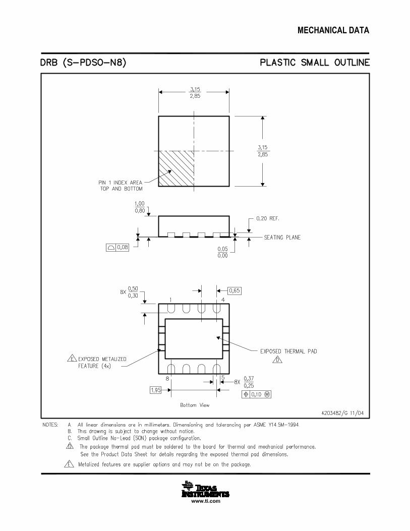
• Internal Bootstrap Diode signal. Systems without 3-state featured controllerscan use enable/power good input/output to hold both• Economical SOIC-8 and Thermally Enhancedoutputs low during shutting down.3-mm x 3-mm DFN-8 Packages
• High Performance Replacement for Popular The TPS28225 is offered in an economical SOIC-83-State Input Drivers and thermally enhanced low-size Dual Flat No-Lead
(DFN-8) packages. The driver is specified in theextended temperature range of –40°C to 125°C withthe absolute maximum junction temperature 150°C.• Multi-Phase DC-to-DC Converters with
Analog or Digital Control• Desktop and Server VRMs and EVRDs• Portable/Notebook Regulators• Synchronous Rectification for Isolated Power
Supplies
Please be aware that an important notice concerning availability, standard warranty, and use in critical applications of TexasInstruments semiconductor products and disclaimers thereto appears at the end of this data sheet.
PRODUCTION DATA information is current as of publication date. Copyright © 2006, Texas Instruments IncorporatedProducts conform to specifications per the terms of the TexasInstruments standard warranty. Production processing does notnecessarily include testing of all parameters.

www.ti.com
FUNCTIONAL BLOCK DIAGRAM
6
13K
2VDD
EN /PG
BOOT
UGATE
PHASE
LGATE
GND
7
1
8
5
4
VDD27K
3−STATE
INPUT
CIRCUITPWM 3
SHOOT −
THROUGH
PROTECTION
THERMAL
SD
HLD−OFF
TIME
UVLO
TYPICAL APPLICATIONS
3
3
2BOOT
UGATE
PHASE
LGATE
GND
1
8
5
4
6 VDD
ENBL7
PWM3
OUT
FB
3GND
3
TPS28225
VDD (4.5 V to 8 V) VIN (3 V to 32 V − VDD)
VOUTVCC
TPS40200
TPS28225
SLUS710–MAY 2006
One-Phase POL Regulator
2 Submit Documentation Feedback

www.ti.com
PWM
CONTROLLER
ISOLATION
AND
FEEDBACK
CO
NT
RO
L
DRIVE
LO
DRIVE
HI
HI
LI
HB
HO
HS
LO
2BOOT
UGATE
PHASE
LGATE
GND
1
8
5
4
3
VDD
EN/PG7
PWM
6
LINEAR
REG.
VDD (4.5 V to 8 V)
VOUT = 3.3 V
35 V to 75V
12 V
Primary High SideVDD High Voltage Driver
VSS
TPS28255
TPS28225
SLUS710–MAY 2006
TYPICAL APPLICATIONS (continued)
Driver for Synchronous Rectification with Complementary Driven MOSFETs
3Submit Documentation Feedback

www.ti.com
5
4
7 3
8
1
2
2BOOT
UGATE
PHASE
LGATE
GND
1
8
5
4
6 VDD
EN/PG7
PWM3
2BOOT
UGATE
PHASE
LGATE
GND
1
8
5
4
6 VDD
EN/PG7
PWM3
VIN
PWM 4
GND
VOUT
PWM1
8PWM3
Enable
PWM2
To Driver
To Driver
GNDS
To Controller
CSCNCS 4
To Controller
CS 1
VDD (4.5 V to 8 V) VIN (3 V to 32 V − VDD)
TPS28225
TPS28225
TP
S4
00
9x
or
an
y o
the
r a
na
log
or
dig
ita
l c
on
tro
lle
r
VOUT
TPS28225
SLUS710–MAY 2006
TYPICAL APPLICATIONS (continued)
Multi-Phase Synchronous Buck Converter
ORDERING INFORMATION (1) (2) (3)
TEMPERATURE RANGE, TA = TJ PACKAGE TAPE AND REEL QTY. PART NUMBER
Plastic 8-pin SOIC (D) 250 TPS28225DT
Plastic 8-pin SOIC (D) 2500 TPS28225DR-40°C to 125°C
Plastic 8-pin DFN (DRB) 250 TPS28225DRBT
Plastic 8-pin DFN (DRB) 3000 TPS28225DRBR
(1) SOIC-8 (D) and DFN-8 (DRB) packages are available taped and reeled. Add T suffix to device type (e.g. TPS28225DT) to order tapeddevices and suffix R to device type to order reeled devices.
(2) The SOIC-8 (D) and DFN-8 (DRB) package uses in Pb-Free lead finish of Pd-Ni-Au which is compatible with MSL level 1 at 255°C to260°C peak reflow temperature to be compatible with either lead free or Sn/Pb soldering operations.
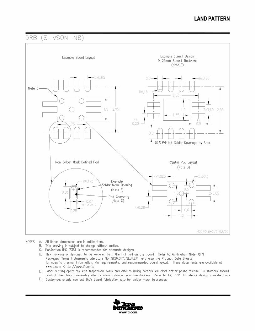
(3) In the DFN package, the pad underneath the center of the device is a thermal substrate. The PCB “thermal land” design for thisexposed die pad should include thermal vias that drop down and connect to one or more buried copper plane(s). This combination ofvias for vertical heat escape and buried planes for heat spreading allows the DFN to achieve its full thermal potential. This pad shouldbe either grounded for best noise immunity, and it should not be connected to other nodes.
4 Submit Documentation Feedback
www.ti.com
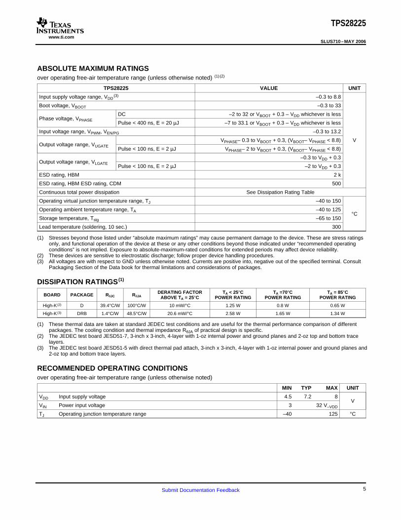
ABSOLUTE MAXIMUM RATINGS
DISSIPATION RATINGS (1)
RECOMMENDED OPERATING CONDITIONS
TPS28225
SLUS710–MAY 2006
over operating free-air temperature range (unless otherwise noted) (1) (2)
TPS28225 VALUE UNIT
Input supply voltage range, VDD(3) –0.3 to 8.8
Boot voltage, VBOOT –0.3 to 33
DC –2 to 32 or VBOOT + 0.3 – VDD whichever is lessPhase voltage, VPHASE
Pulse < 400 ns, E = 20 µJ –7 to 33.1 or VBOOT + 0.3 – VDD whichever is less
Input voltage range, VPWM, VEN/PG –0.3 to 13.2
VPHASE– 0.3 to VBOOT + 0.3, (VBOOT– VPHASE < 8.8) VOutput voltage range, VUGATE
Pulse < 100 ns, E = 2 µJ VPHASE– 2 to VBOOT + 0.3, (VBOOT– VPHASE < 8.8)
–0.3 to VDD + 0.3Output voltage range, VLGATE
Pulse < 100 ns, E = 2 µJ –2 to VDD + 0.3
ESD rating, HBM 2 k
ESD rating, HBM ESD rating, CDM 500
Continuous total power dissipation See Dissipation Rating Table
Operating virtual junction temperature range, TJ –40 to 150
Operating ambient temperature range, TA –40 to 125°C
Storage temperature, Tstg –65 to 150
Lead temperature (soldering, 10 sec.) 300
(1) Stresses beyond those listed under “absolute maximum ratings” may cause permanent damage to the device. These are stress ratingsonly, and functional operation of the device at these or any other conditions beyond those indicated under “recommended operatingconditions” is not implied. Exposure to absolute-maximum-rated conditions for extended periods may affect device reliability.
(2) These devices are sensitive to electrostatic discharge; follow proper device handling procedures.(3) All voltages are with respect to GND unless otherwise noted. Currents are positive into, negative out of the specified terminal. Consult
Packaging Section of the Data book for thermal limitations and considerations of packages.
DERATING FACTOR TA < 25°C TA =70°C TA = 85°CBOARD PACKAGE RθJC RθJA ABOVE TA = 25°C POWER RATING POWER RATING POWER RATING
High-K (2) D 39.4°C/W 100°C/W 10 mW/°C 1.25 W 0.8 W 0.65 W
High-K (3) DRB 1.4°C/W 48.5°C/W 20.6 mW/°C 2.58 W 1.65 W 1.34 W
(1) These thermal data are taken at standard JEDEC test conditions and are useful for the thermal performance comparison of differentpackages. The cooling condition and thermal impedance RθJA of practical design is specific.
(2) The JEDEC test board JESD51-7, 3-inch x 3-inch, 4-layer with 1-oz internal power and ground planes and 2-oz top and bottom tracelayers.
(3) The JEDEC test board JESD51-5 with direct thermal pad attach, 3-inch x 3-inch, 4-layer with 1-oz internal power and ground planes and2-oz top and bottom trace layers.
over operating free-air temperature range (unless otherwise noted)
MIN TYP MAX UNIT
VDD Input supply voltage 4.5 7.2 8V
VIN Power input voltage 3 32 V–VDD
TJ Operating junction temperature range –40 125 °C
5Submit Documentation Feedback
www.ti.com
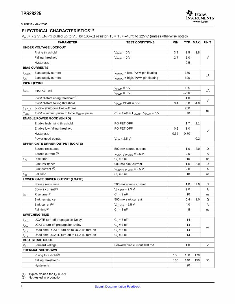
ELECTRICAL CHARACTERISTICS (1)
TPS28225
SLUS710–MAY 2006
VDD = 7.2 V, EN/PG pulled up to VDD by 100-kΩ resistor, TA = TJ = –40°C to 125°C (unless otherwise noted)
PARAMETER TEST CONDITIONS MIN TYP MAX UNIT
UNDER VOLTAGE LOCKOUT
Rising threshold VPWM = 0 V 3.2 3.5 3.8
Falling threshold VPWM = 0 V 2.7 3.0 V
Hysteresis 0.5
BIAS CURRENTS
IDD(off) Bias supply current VEN/PG = low, PWM pin floating 350µA
IDD Bias supply current VEN/PG = high, PWM pin floating 500
INPUT (PWM)
VPWM = 5 V 185IPWM Input current µA
VPWM = 0 V –200
PWM 3-state rising threshold (2) 1.0V
PWM 3-state falling threshold VPWM PEAK = 5 V 3.4 3.8 4.0
tHLD_R 3-state shutdown Hold-off time 250ns
TMIN PWM minimum pulse to force UGATE pulse CL = 3 nF at UGATE , VPWM = 5 V 30
ENABLE/POWER GOOD (EN/PG)
Enable high rising threshold PG FET OFF 1.7 2.1
Enable low falling threshold PG FET OFF 0.8 1.0V
Hysteresis 0.35 0.70
Power good output VDD = 2.5 V 0.2
UPPER GATE DRIVER OUTPUT (UGATE)
Source resistance 500 mA source current 1.0 2.0 Ω
Source current (2) VUGATE-PHASE = 2.5 V 2.0 A
tRU Rise time CL = 3 nF 10 ns
Sink resistance 500 mA sink current 1.0 2.0 Ω
Sink current (2) VUGATE-PHASE = 2.5 V 2.0 A
tFU Fall time CL = 3 nF 10 ns
LOWER GATE DRIVER OUTPUT (LGATE)
Source resistance 500 mA source current 1.0 2.0 Ω
Source current (2) VLGATE = 2.5 V 2.0 A
tRL Rise time (2) CL = 3 nF 10 ns
Sink resistance 500 mA sink current 0.4 1.0 Ω
Sink current (2) VLGATE = 2.5 V 4.0 A
Fall time (2) CL = 3 nF 5 ns
SWITCHING TIME
tDLU UGATE turn-off propagation Delay CL = 3 nF 14
tDLL LGATE turn-off propagation Delay CL = 3 nF 14ns
tDTU Dead time LGATE turn-off to UGATE turn-on CL = 3 nF 14
tDTL Dead time UGATE turn-off to LGATE turn-on CL = 3 nF 14
BOOTSTRAP DIODE
VF Forward voltage Forward bias current 100 mA 1.0 V
THERMAL SHUTDOWN
Rising threshold (2) 150 160 170
Falling threshold (2) 130 140 150 °C
Hysteresis 20
(1) Typical values for TA = 25°C(2) Not tested in production
6 Submit Documentation Feedback

www.ti.com
DEVICE INFORMATION
1
2
3
4
8
7
6
5
UGATE
BOOT
PWM
GND
PHASE
EN/PG
VDD
LGATE
5
3
7
6
81
2BOOT
PWM VDD
EN/PG
LG AT EGND
U G ATE PHASE
4
ExposedThermalDie Pad
6
13K
2VDD
EN /PG
BOOT
UGATE
PHASE
LGATE
GND
7
1
8
5
4
VDD27K3−STATE
INPUT
CIRCUITPWM 3
SHOOT −THROUGH
PROTECTION
THERMALSD
HLD−OFFTIME
UVLO
TPS28225
SLUS710–MAY 2006
SOIC-8 Package (top view)
DRB-8 Package (top view)
FUNCTIONAL BLOCK DIAGRAM
A. For the TPS28224DRB device the thermal PAD on the bottom side of package must be soldered and connected tothe GND pin and to the GND plane of the PCB in the shortest possible way. See Recommended Land Pattern in theApplication section.
7Submit Documentation Feedback

www.ti.com
Normal switching
PWM
LGATE
UGATE
3 −State
window
90 %
10 %
tDLL
50 %
tFL
50 %
tPWM_MIN
tDTU
90 %
10 %
tRU90 %
10 %
tDLU
tFU
tDTL90 %
10 %
tRL
tHLD_R
90 %
10 %
90 %
90 %
tHLD_F
Enter into 3 −State
at PWM riseExit 3 −State
Enter into 3 −State
at PWM fall
PWM Low and High after 3 −
State to allow Bootstrap
Capacitor Restore Charge
TRUTH TABLE
TPS28225
SLUS710–MAY 2006
TERMINAL FUNCTIONS
TERMINALI/O DESCRIPTION
SOIC-8 DRB-8 NAME
1 1 UGATE O Upper gate drive sink/source output. Connect to gate of high-side power N-Channel MOSFET.
Floating bootstrap supply pin for the upper gate drive. Connect the bootstrap capacitor between2 2 BOOT I/O this pin and the PHASE pin. The bootstrap capacitor provides the charge to turn on the upper
MOSFET.
The PWM signal is the control input for the driver. The PWM signal can enter three distinct states3 3 PWM I during operation, see the 3-state PWM Input section under DETAILED DESCRIPTION for further
details. Connect this pin to the PWM output of the controller.
4 4 GND — Ground pin. All signals are referenced to this node.
Exposed Thermal — Connect directly to the GND for better thermal performance and EMIdie pad pad
Lower gate drive sink/source output. Connect to the gate of the low-side power N-Channel5 5 LGATE O MOSFET.
6 6 VDD I Connect this pin to a 5-V bias supply. Place a high quality bypass capacitor from this pin to GND.
Enable/Power Good input/output pin with 1MΩ impedance. Connect this pin to HIGH to enableand LOW to disable the IC. When disabled, the device draws less than 350µA bias current. If the7 7 EN/PG I/O VDD is below UVLO threshold or over temperature shutdown occurs, this pin is internally pulledlow.
Connect this pin to the source of the upper MOSFET and the drain of the lower MOSFET. This pin8 8 PHASE I provides a return path for the upper gate driver.
TIMING DIAGRAM
VDD FALLING > 3 V AND TJ < 150°C
VDD RISING < 3.5 V EN/PG FALLING > 1.0 VPIN EN/PG RISINGOR TJ > 160°C PWM > 1.5 V AND PWM SIGNAL SOURCE IMPEDANCE< 1.7 V PWM < 1 V TRISE/TFALL < 200 ns >40 kΩ FOR > 250ns (3-State) (1)
LGATE Low Low High Low Low
UGATE Low Low Low High Low
EN/PG Low
(1) To exit the 3-state condition, the PWM signal should go low. One Low PWM input signal followed by one High PWM input signal isrequired before re-entering the 3-state condition.
8 Submit Documentation Feedback

www.ti.com
TYPICAL CHARACTERISTICS
−40 125
300
340
380
420
460
500
25
320
360
400
440
480
TJ − Temperature − °C
I DD
(off)
− B
ias
Sup
ply
− µA
2.00
2.75
3.25
4.00
2.25
2.50
3.00
3.50
3.75
UV
LO −
Und
er V
olta
ge L
ocko
ut −
V
−40 12525
Falling
Rising
TJ − Temperature − °C
0.0
PW
M −
PW
M 3
−Sta
te T
hres
hold
− V
−40 12525
2.0
3.0
5.0
0.5
1.0
2.5
2.5
4.5
1.5
4.0 Falling
Rising
TJ − Temperature − °C−40 12525
0.00
0.75
1.25
2.00
0.25
0.50
1.00
1.50
1.75
Falling
Rising
TJ − Temperature − °C
EN
/PG
− E
nabl
e/P
ower
Goo
d −
V
TPS28225
SLUS710–MAY 2006
BIAS SUPPLY CURRENT UNDER VOLTAGE LOCKOUT THRESHOLDvs vs
TEMPERATURE TEMPERATURE(VEN/PG = Low, PWM Input Floating, VDD = 7.2V)
Figure 1. Figure 2.
ENABLE/POWER GOOD THRESHOLD PWM 3-STATE THRESHOLDS, (5-V Input Pulses)vs vs
TEMPERATURE (VDD = 7.2 V) TEMPERATURE, (VDD = 7.2 V)
Figure 3. Figure 4.
9Submit Documentation Feedback

www.ti.com
0
−40 12525
0.75
1.25
2.00
0.25
0.50
1.00
1.50
1.75
RSINK
RSOURCE
TJ − Temperature − °C
RO
UT
− O
utpu
t Im
peda
nce
− Ω
0
−40 12525
0.75
1.25
2.00
0.25
0.50
1.00
1.50
1.75
RSINK
RSOURCE
TJ − Temperature − °C
RO
UT
− O
utpu
t Im
peda
nce
− Ω
−40 12525
4
6
10
12
14
5
7
9
11
13
8
Falling
Rising
TJ − Temperature − °C
t RL/
t FL
− R
ise
and
Fal
l Tim
e −
ns
6
8
11
13
15
7
9
10
12
14
−40 12525
Falling
Rising
TJ − Temperature − °C
t RU
/tFU
− R
ise
and
Fal
l Tim
e −
ns
TPS28225
SLUS710–MAY 2006
TYPICAL CHARACTERISTICS (continued)
UGATE DC OUTPUT IMPEDANCE LGATE DC OUTPUT IMPEDANCEvs vs
TEMPERATURE, (VDD = 7.2 V) TEMPERATURE (VDD = 7.2 V)
Figure 5. Figure 6.
UGATE RISE AND FALL TIME LGATE RISE AND FALL TIMEvs vs
TEMPERATURE (VDD = 7.2 V, CLOAD = 3 nF) TEMPERATURE (VDD = 7.2 V, CLOAD = 3 nF)
Figure 7. Figure 8.
10 Submit Documentation Feedback

www.ti.com
0
20
25
30
5
10
15
−40 12525
LGATE
UGATE
TJ − Temperature − °C
t DLU
/tD
LL −
UG
ATE
and
LG
ATE
− n
s
−40 12525
0.0
12.5
17.5
20.0
2.5
7.5
10.0
5.0
15.0
LGATE
UGATE
TJ − Temperature − °C
t DTU
/tD
TL −
UG
ATE
and
LG
ATE
− n
s
0.5
0.8
1.0
1.3
0.6
0.7
0.9
1.1
1.2
−40 12525
TJ − Temperature − °C
VF
− F
orw
ard
Vol
tage
− V
0
5
25
30
10
15
20
−40 12525
TJ − Temperature − °C
TM
IN −
Min
imum
Sho
rt P
ulse
− n
s
TPS28225
SLUS710–MAY 2006
TYPICAL CHARACTERISTICS (continued)
UGATE AND LGATE (Turning OFF Propagation Delays) UGATE AND LGATE (Dead Time)vs vs
TEMPERTURE (VDD = 7.2 V, CLOAD = 3 nF) TEMPERTURE (VDD = 7.2 V, CLOAD = 3 nF)
Figure 9. Figure 10.
UGATE MINIMUM SHORT PULSE BOOTSTRAP DIODE FORWARD VOLTAGEvs vs
TEMPERATURE (VDD = 7.2 V, CLOAD = 3 nF) TEMPERATURE (VDD = 7.2 V, IF = 100 mA)
Figure 11. Figure 12.
11Submit Documentation Feedback

www.ti.com
0
200
1000
1200
400
600
800
100 300 500 700 1500 1700900 1100 19001300
UG = 50 nCLG = 50 nC
UG = 25 nCLG = 50 nC
UG = 25 nCLG = 100 nC
FSW − Switching Frequency − kHz
PD
ISS −
Dis
sipa
ted
Pow
er −
mW
0
15
5
10
100 300 500 700 1500 1700900 1100 19001300
FSW − Switching Frequency − kHz
I DD
− B
ias
Sup
ply
Cur
rent
− m
A
PWM
UGATE
LGATE
VDD = 7.2 V, CL = 3 nF, TJ = 25°C
t − Time − 10 ns/div .
Vol
tage
− 5
V/d
iv. PWM
UGATE
LGATE
VDD = 7.2 V, CL = 3 nF, TJ = 25°C
t − Time − 10 ns/div .
Vol
tage
− 5
V/d
iv.
TPS28225
SLUS710–MAY 2006
TYPICAL CHARACTERISTICS (continued)
BIAS SUPPLY CURRENT DRIVER DISSIPATED POWERvs vs
SWITCHING FREQUENCY SWITCHING FREQUENCY(VDD = 7.2 V, No Load, TJ = 25°C) (Different Load Charge, VDD = 7.2 V, TJ = 25°C)
Figure 13. Figure 14.
PWM INPUT RISING SWITCHING WAVEFORMS PWM INPUT FALLING SWITCHING WAVEFORMS
Figure 15. Figure 16.
12 Submit Documentation Feedback
www.ti.com
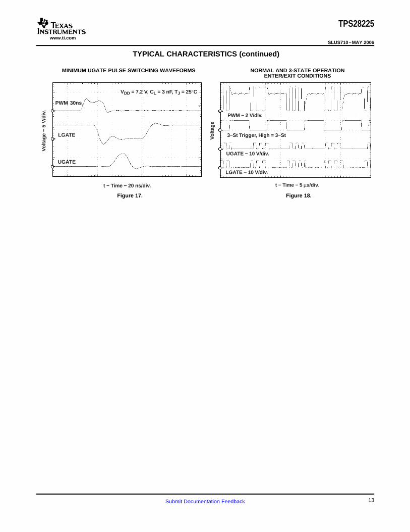
PWM 30ns
UGATE
LGATE
VDD = 7.2 V, CL = 3 nF, TJ = 25°C
t − Time − 20 ns/div .
Vol
tage
− 5
V/d
iv.
PWM − 2 V/div.
3−St Trigger , High = 3−St
UGATE − 10 V/div.
LGATE − 10 V/div.
Vol
tage
t − Time − 5 µs/div.
TPS28225
SLUS710–MAY 2006
TYPICAL CHARACTERISTICS (continued)
MINIMUM UGATE PULSE SWITCHING WAVEFORMS NORMAL AND 3-STATE OPERATIONENTER/EXIT CONDITIONS
Figure 17. Figure 18.
13Submit Documentation Feedback

www.ti.com
DETAILED DESCRIPTION
UNDER VOLTAGE LOCKOUT (UVLO)
OUTPUT ACTIVE LOW
ENABLE/POWER GOOD
Thermal SD
UVLO
7EN/PG
6System
Controller 20 kΩ
VCC VDD = 4.5 V to 8 V
Driver TPS28225
1 kΩ
1 M
RDS(on) = 1 kΩ
2 V Rise1 V Fall
TPS28225
SLUS710–MAY 2006
The TPS28225 incorporates an under voltage lockout circuit that keeps the driver disabled and external powerFETs in an OFF state when the input supply voltage VDD is insufficient to drive external power FETs reliably.During power up, both gate drive outputs remain low until voltage VDD reaches UVLO threshold, typically 3.5V.Once the UVLO threshold is reached, the condition of gate drive outputs is defined by the input PWM andEN/PG signals. During power down the UVLO threshold is set lower, typically 3.0V. The 0.5-V hysteresis isselected to prevent the driver from turning ON and OFF while the input voltage crosses UVLO thresholds,especially with low slew rate. The TPS28225 has the ability to send a signal back to the system controller thatthe input supply voltage VDD is insufficient by internally pulling down the EN/PG pin. The TPS28225 releasesEN/PG pin immediately after the VDD has risen above the UVLO threshold.
The output active low circuit effectively keeps the gate outputs low even if the driver is not powered up. Thisprevents open gate conditions on the external power FETs and accidental turn ON when the main power stagesupply voltage is applied before the driver is powered up. For the simplicity, the output active low circuit isshown in a block diagram as the resistor connected between LGATE and GND pins with another one connectedbetween UGATE and PHASE pins.
The Enable/Power Good circuit allows the TPS28225 to follow the PWM input signal when the voltage at EN/PGpin is above 2.1 V maximum. This circuit has a unique two-way communication capability. This is illustrated byFigure 19.
Figure 19. Enable/Power Good Circuit
The EN/PG pin has approximately 1-kΩ internal series resistor. Pulling EN/PG high by an external ≥ 20-kΩresistor allows two-way communication between controller and driver. If the input voltage VDD is below UVLOthreshold or thermal shut down occurs, the internal MOSFET pulls EN/PG pin to GND through 1-kΩ resistor.The voltage across the EN/PG pin is now defined by the resistor divider comprised by the external pull upresistor, 1-kΩ internal resistor and the internal FET having 1kΩ RDS(on). Even if the system controller allows thedriver to start by setting its own enable output transistor OFF, the driver keeps the voltage at EN/PG low. LowEN/PG signal indicates that the driver is not ready yet because the supply voltage VDD is low or that the driver isin thermal shutdown mode. The system controller can arrange the delay of PWM input signals coming to thedriver until the driver releases EN/PG pin. If the input voltage VDD is back to normal, or the driver is cooled downbelow its lower thermal shutdown threshold, then the internal MOSFET releases the EN/PG pin and normaloperation resumes under the external Enable signal applied to EN/PG input. Another feature includes an internal1MΩ resistor that pulls EN/PG pin low and disables the driver in case the system controller accidentally losesconnection with the driver. This could happen if, for example, the system controller is located on a separate PCBdaughter board.
14 Submit Documentation Feedback
www.ti.com
3-STATE INPUT
TPS28225
SLUS710–MAY 2006
DETAILED DESCRIPTION (continued)
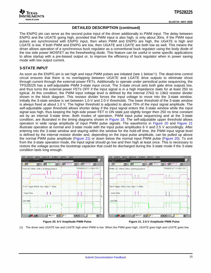
The EN/PG pin can serve as the second pulse input of the driver additionally to PWM input. The delay betweenEN/PG and the UGATE going high, provided that PWM input is also high, is only about 30ns. If the PWM inputpulses are synchronized with EN/PG input, then when PWM and EN/PG are high, the UGATE is high andLGATE is low. If both PWM and EN/PG are low, then UGATE and LGATE are both low as well. This means thedriver allows operation of a synchronous buck regulator as a convertional buck regulator using the body diode ofthe low side power MOSFET as the freewheeling diode. This feature can be useful in some specific applicationsto allow startup with a pre-biased output or, to improve the efficiency of buck regulator when in power savingmode with low output current.
As soon as the EN/PG pin is set high and input PWM pulses are initiated (see 1 below (1)). The dead-time controlcircuit ensures that there is no overlapping between UGATE and LGATE drive outputs to eliminate shootthrough current through the external power FETs. Additionally to operate under periodical pulse sequencing, theTPS28225 has a self-adjustable PWM 3-state input circuit. The 3-state circuit sets both gate drive outputs low,and thus turns the external power FETs OFF if the input signal is in a high impedance state for at least 250 nstypical. At this condition, the PWM input voltage level is defined by the internal 27kΩ to 13kΩ resistor dividershown in the block diagram. This resistor divider forces the input voltage to move into the 3-state window.Initially the 3-state window is set between 1.0-V and 2.0-V thresholds. The lower threshold of the 3-state windowis always fixed at about 1.0 V. The higher threshold is adjusted to about 75% of the input signal amplitude. Theself-adjustable upper threshold allows shorter delay if the input signal enters the 3-state window while the inputsignal was high, thus keeping the high-side power FET in ON state just slightly longer then 250 ns time constantset by an internal 3-state timer. Both modes of operation, PWM input pulse sequencing and at the 3-statecondition, are illustrated in the timing diagrams shown in Figure 18. The self-adjustable upper threshold allowsoperation in wide range amplitude of input PWM pulse signals. The waveforms in Figure 20 and Figure 21illustrate operation at normal and 3-state mode with the input pulse amplitudes 6 V and 2.5 V accordingly. Afterentering into the 3-state window and staying within the window for the hold-off time, the PWM input signal levelis defined by the internal resistor divider and, depending on the input pulse amplitude, can be pulled up abovethe normal PWM pulse amplitude (Figure 21) or down below the normal input PWM pulse (Figure 20). To exitfrom the 3-state operation mode, the input signal should go low and then high at least once. This is necessary torestore the voltage across the bootstrap capacitor that could be discharged during the 3-state mode if the 3-statecondition lasts long enough.
Figure 20. 6-V Amplitude PWM Pulse Figure 21. 2.5-V Amplitude PWM Pulse
(1) The driver sets UGATE low and LGATE high when PWM is low. When the PWM goes high, UGATE goes high and LGATE goes low.
15Submit Documentation Feedback

www.ti.com
TPS28225
SLUS710–MAY 2006
DETAILED DESCRIPTION (continued)
IMPORTANT NOTE: Any external resistor between PWM input and GND with the value lower than 40kΩ caninterfere with the 3-state thresholds. If the driver is intended to operate in the 3-state mode, any resistor below40kΩ at the PWM and GND should be avoided. A resistor lower than 3.5kΩ connected between the PWM andGND completely disables the 3-state function. In such case, the 3-state window shrinks to zero and the lower3-state threshold becomes the boundary between the UGATE staying low and LGATE being high and vice versadepending on the PWM input signal applied. It is not necessary to use a resistor <3.5kΩ to avoid the 3-statecondition while using a controller that is 3-state capable. If the rise and fall time of the input PWM signal isshorter than 250ns, then the driver never enter into the 3-state mode.
In the case where the low-side MOSFET of a buck converter stays on during shutdown, the 3-state feature canbe fused to avoid negative resonent voltage across the output capacitor. This feature also can be used duringstart up with a pre-biased output in the case where pulling the output low during the startup is not allowed due tosystem requirements. If the system controller does not have the 3-state feature and never goes into thehigh-impedance state, then setting the EN/PG signal low will keep both gate drive outputs low and turn both low-and high-side MOSFETs OFF during the shut down and start up with the pre-biased output.
The self-adjustable input circuit accepts wide range of input pulse amplitudes (2V up to 13.2V) allowing use of avariety of controllers with different outputs including logic level. The wide PWM input voltage allows someflexibility if the driver is used in secondary side synchronous rectifier circuit. The operation of the TPS28225 witha 12-V input PWM pulse amplitude, and with VDD = 7.2V and VDD = 5V respectively is shown in Figure 22 andFigure 23.
Figure 22. 12-V PWM Pulse at VDD = 7.2 V Figure 23. 12-V PWM Pulse at VDD = 5 V
16 Submit Documentation Feedback

www.ti.com
BOOTSTRAP DIODE
UPPER AND LOWER GATE DRIVERS
DEAD TIME CONTROL
THERMAL SHUTDOWN
TPS28225
SLUS710–MAY 2006
DETAILED DESCRIPTION (continued)
The bootstrap diode provides the supply voltage for the UGATE driver by charging the bootstrap capacitorconnected between BOOT and PHASE pins from the input voltage VDD when the low-side FET is in ON state.At the very initial stage when both power FETs are OFF, the bootstrap capacitor is pre-charged through thispath including the PHASE pin, output inductor and large output capacitor down to GND. The forward voltagedrop across the diode is only 1.0V at bias current 100 mA. This allows quick charge restore of the bootstrapcapacitor during the high-frequency operation.
The upper and lower gate drivers charge and discharge the input capacitance of the power MOSFETs to allowoperation at switching frequencies up to 2 MHz. The output stage consists of a P-channel MOSFET providingsource output current and an N-channel MOSFET providing sink current through the output stage. The ON stateresistances of these MOSFETs are optimized for the synchronous buck converter configuration working with lowduty cycle at the nominal steady state condition. The UGATE output driver is capable of propagating PWM inputpuses of less than 30-ns while still maintaining proper dead time to avoid any shoot through current conditions.The waveforms related to the narrow input PWM pulse operation are shown in Figure 17.
The dead-time control circuit is critical for highest efficiency and no shoot through current operation througoutthe whole duty cycle range with the different power MOSFETs. By sensing the output of driver going low, thiscircuit does not allow the gate drive output of another driver to go high until the first driver output falls below thespecified threshold. This approach to control the dead time is called adaptive. The overall dead time alsoincludes the fixed portion to ensure that overlapping never exists. The typical dead time is around 14 ns,although it varies over the driver internal tolerances, layout and external MOSFET parasitic inductances. Theproper dead time is maintained whenever the current through the output inductor of the power stage flows in theforward or reverse direction. Reverse current could happen in a buck configuration during the transients or whiledynamically changing the output voltage on the fly, as some microprocessors require. Because the dead timedoes not depend on inductor current direction, this driver can be used both in buck and boost regulators or inany bridge configuration where the power MOSFETs are switching in a complementary manner. Keeping thedead time at short optimal level boosts efficiency by 1% to 2% depending on the switching frequency. Measuredswitching waveforms in one of the practical designs show 10-ns dead time for the rising edge of PHASE nodeand 22 ns for the falling edge (Figure 29 and Figure 30 in the Application Section of the data sheet).
Large non-optimal dead time can cause duty cycle modulation of the dc-to-dc converter during the operationpoint where the output inductor current changes its direction right before the turn ON of the high-side MOSFET.This modulation can interfere with the controller operation and it impacts the power stage frequency responsetransfer function. As the result, some output ripple increase can be observed. The TPS28225 driver is designedwith the short adaptive dead time having fixed delay portion that eliminates risk of the effective duty cyclemodulation at the described boundary condition.
If the junction temperature exceeds 160°C, the thermal shutdown circuit will pull both gate driver outputs low andthus turning both, low-side and high-side power FETs OFF. When the driver cools down below 140°C after athermal shutdown, then it resumes its normal operation and follows the PWM input and EN/PG signals from theexternal control circuit. While in thermal shutdown state, the internal MOSFET pulls the EN/PG pin low, thussetting a flag indicating the driver is not ready to continue normal operation. Normally the driver is located closeto the MOSFETs, and this is usually the hottest spots on the PCB. Thus, the thermal shutdown feature ofTPS28225 can be used as an additional protection for the whole system from overheating.
17Submit Documentation Feedback
www.ti.com
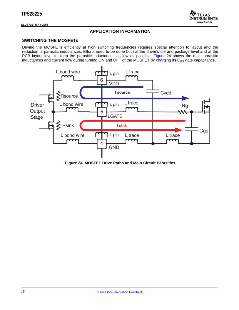
APPLICATION INFORMATION
SWITCHING THE MOSFETs
4
5
GND
6VDD
LGATE
Cvdd
L bond wire
Rsink
Rsource
L pin
L trace
L bond wire
L bond wire
Driver
Output
Stage
L pin
L pin
L trace
I sink
L traceCgs
Rg
L trace
I source
TPS28225
SLUS710–MAY 2006
Driving the MOSFETs efficiently at high switching frequencies requires special attention to layout and thereduction of parasitic inductances. Efforts need to be done both at the driver’s die and package level and at thePCB layout level to keep the parasitic inductances as low as possible. Figure 24 shows the main parasiticinductances and current flow during turning ON and OFF of the MOSFET by charging its CGS gate capacitance.
Figure 24. MOSFET Drive Paths and Main Circuit Parasitics
18 Submit Documentation Feedback

www.ti.com
VoltageCurrent
t − Time − ns
LGA
TE
Fal
ling,
V o
r A
LGA
TE
Fal
ling,
V o
r A
LGATE Current, A
Voltage
Current
t − Time − ns
UG
AT
E F
allin
g, V
UG
AT
E F
allin
g, V
UGATE Current, A
TPS28225
SLUS710–MAY 2006
APPLICATION INFORMATION (continued)
The ISOURCE current charges the gate capacitor and the ISINK current discharges it. The rise and fall time ofvoltage across the gate defines how quickly the MOSFET can be switched. The timing parameters specified indatasheet for both upper and lower driver are shown in Figure 15 and Figure 16 where 3-nF load capacitor hasbeen used for the characterization data. Based on these actual measurements, the analytical curves inFigure 25 and Figure 26 show the output voltage and current of upper and low side drivers during thedischarging of load capacitor. The left waveforms show the voltage and current as a function of time, while theright waveforms show the relation between the voltage and current during fast switching. These waveformsshow the actual switching process and its limitations because of parasitic inductances. The static VOUT/ IOUTcurves shown in many datasheets and specifications for the MOSFET drivers do not replicate actual switchingcondition and provide limited information for the user.
Figure 25. LGATE Turning Off Voltage and Sink Current vs Time (Related Switching Diagram (right))
Figure 26. UGATE Turning Off Voltage and Sink Current vs Time (Related Switching Diagram (right)_
19Submit Documentation Feedback

www.ti.com
Layout Recommendations
TPS28225
SLUS710–MAY 2006
APPLICATION INFORMATION (continued)
Turning Off of the MOSFET needs to be done as fast as possible to reduce switching losses. For this reason theTPS28225 driver has very low output impedance specified as 0.4Ω typ for lower driver and 1Ω typ for upperdriver at dc current. Assuming 8-V drive voltage and no parasitic inductances, one can expect an initial sinkcurrent amplitude of 20A and 8A respectively for the lower and upper drivers. With pure R-C discharge circuit forthe gate capacitor, the voltage and current waveforms are expected to be exponential. However, because ofparasitic inductances, the actual waveforms have some ringing and the peak current for the lower driver is about4A and about 2.5A for the upper driver (Figure 25 and Figure 26). The overall parasitic inductance for the lowerdrive path is estimated as 4nH and for the upper drive path as 6nH. The internal parasitic inductance of thedriver, which includes inductances of bonded wires and package leads, can be estimated for SOIC-8 packageas 2nH for lower gate and 4nH for the upper gate. Use of DFN-8 package reduces the internal parasiticinductances by approximately 50%.
To improve the switching characteristicsand efficiency of a design, the following layout rules need to be followed.• Locate the driver as close as possible to the MOSFETs.• Locate the VDD and bootstrap capacitors as close as possible to the driver.• Pay special attention to the GND trace. Use the thermal pad of the DFN-8 package as the GND by
connecting it to the GND pin. The GND trace or pad from the driver goes directly to the source of theMOSFET but should not include the high current path of the main current flowing through the drain andsource of the MOSFET.
• Use a similar rule for the PHASE node as for the GND.• Use wide traces for UGATE and LGATE closely following the related PHASE and GND traces. Eighty to 100
mils width is preferable where possible.• Use at least 2 or more vias if the MOSFET driving trace needs to be routed from one layer to another. For
the GND the number of vias are determined not only by the parasitic inductance but also by therequirements for the thermal pad.
• Avoid PWM and enable traces going close to the PHASE node and pad where high dV/dT voltage caninduce significant noise into the relatively high impedance leads.
It should be taken into account that poor layout can cause 3% to 5% less efficiency versus a good layout designand can even decrease the reliability of the whole system.
Figure 27. One of Phases Driven by TPS28225 Driver in 4-phase VRM Reference Design
20 Submit Documentation Feedback

www.ti.com
TPS28225
SLUS710–MAY 2006
APPLICATION INFORMATION (continued)
The schematic of one of the phases in a multi-phase synchronous buck regulator and the related layout areshown in Figure 27 and Figure 28. These help to illustrate good design practices. The power stage includes onehigh-side MOSFET Q10 and two low-side MOSFETS (Q8 and Q9). The driver (U7) is located on bottom side ofPCB close to the power MOSFETs. The related switching waveforms during turning ON and OFF of upper FETare shown in Figure 29 and Figure 30. The dead time during turning ON is only 10ns (Figure 29) and 22nsduring turning OFF (Figure 30).
Figure 28. Component Placement Based on Schematic in Figure 27
Figure 29. Phase Rising Edge Switching Waveforms (20ns/div) of the Power Stage in Figure 27
21Submit Documentation Feedback

www.ti.com
LIST OF MATERIALS
TPS28225
SLUS710–MAY 2006
APPLICATION INFORMATION (continued)
Figure 30. Phase Falling Edge Switching Waveforms (10ns/div) of the Power State in Figure 27
The list of materials for this specific example is provided in the table. The component vendors are not limited tothose shown in the table below. It should be notd that, in this example, the power MOSFET packages werechosen with drains on top. The decoupling capacitors C47, C48, C65, and C66 were chosen to have lowprofiles. This allows the designer to meet good layout rules and place a heatsink on top of the FETs using anelectrically isolated and thermally conductive pad.
List of MaterialsREF DES COUNT DESCRIPTION MANUFACTURE PART NUMBER
C47, C48, 4 Capacitor, ceramic, 4.7 µF, 16 V, X5R 10%, low profile 0.95 mm, 1206 TDK C3216X5R1C475KC65, C66
C41, C42 2 Capacitor, ceramic, 10 µF, 16 V, X7R 10%, 1206 TDK C3216X7R1C106K
C50, C51 2 Capacitor, ceramic, 1000 pF, 50 V, X7R, 10%, 0603 Std Std
C23 1 Capacitor, ceramic, 0.22 µF, 16 V, X7R, 10%, 0603 Std Std
C25, C49, 3 Capacitor, ceramic, 1 µF, 16 V, X7R, 10%, '0603 Std StdC71
L3 1 Inductor, SMT, 0.12 µH, 31 A, 0.36 mΩ, 0.400 x 0.276 Pulse PA0511-101
Q8, Q9 2 Mosfet, N-channel, VDS 30 V, RDS 2.4 mΩ, ID 45 A, LFPAK-i Renesas RJK0301DPB-I
Q10 1 Mosfet, N-channel, VDS 30 V, RDS 6.2 mΩ, ID 30 A, LFPAK-i Renesas RJK0305DPB-I
R32 1 Resistor, chip, 0 Ω, 1/10 W, 1%, '0805 Std Std
R51, R52 2 Resistor, chip, 2.2 Ω, 1/10 W, 1%, '0805 Std Std
U7 1 Device, High Frequency 4-A Sink Synchronous Buck MOSFET Driver, Texas Instruments TPS28225DRBDFN-8
22 Submit Documentation Feedback

www.ti.com
EFFICIENCY OF POWER STAGE vs LOAD CURRENT AT DIFFERENT SWITCHING
TI: 400kHz
Ind: 400kHz
5 10 15 25 35
75
90
20 30
80
85
Effi
cien
cy −
%
CL − Load Currnt − A
TI: 500kHz
Ind: 500kHz
5 10 15 25 35
75
90
20 30
80
85
Effi
cien
cy −
%
CL − Load Currnt − A
TI: 600kHz
Ind: 600kHz
5 10 15 25 35
75
90
20 30
80
85
Effi
cien
cy −
%
CL − Load Currnt − A
TPS28225
SLUS710–MAY 2006
FREQUENCIES
Efficiency achieved using TPS28225 driver with 8-V drive at different switching frequencies a similar industry 5-Vdriver using the power stage in Figure 27 is shown in Figure 33, Figure 35, Figure 34, Figure 31 and Figure 32.
EFFICIENCY EFFICIENCYvs vs
LOAD CURRENT LOAD CURRENT
Figure 31. Figure 32.
EFFICIENCYvs
LOAD CURRENT
Figure 33.
23Submit Documentation Feedback

www.ti.com
TI: 700kHzInd: 700kHz
5 10 15 25 35
75
90
20 30
80
85
Effi
cien
cy −
%
CL − Load Currnt − A
TI: 800kHzInd: 800kHz
5 10 15 25 35
75
90
20 30
80
85
Effi
cien
cy −
%
CL − Load Currnt − A
400 500 700 800
0.0
1.5
2.0
600
0.5
1.0
DRIVE LOSSvs
SWITCHING FREQUENCY
FSW − Switching Frequency − kHz
12−VEstimation
SOIC−8PackageLimit at 45 °C
8−VTPS28225
5−VInd. Std.
DL
− D
rive
Loss
− W
TPS28225
SLUS710–MAY 2006
EFFICIENCY EFFICIENCYvs vs
LOAD CURRENT LOAD CURRENT
Figure 34. Figure 35.
When using the same power stage, the driver with the optimal drive voltage and optimal dead time can boostefficiency up to 5%. The optimal 8-V drive voltage versus 5-V drive contributes 2% to 3% efficiency increase andthe remaining 1% to 2% can be attributed to the reduced dead time. The 7-V to 8-V drive voltage is optimal foroperation at switching frequency range above 400kHz and can be illustrated by observing typical RDS(on) curvesof modern FETs as a function of their gate drive voltage. This is shown in Figure 36.
Figure 36. RDS(on) of MOSFET as Function of VGS Figure 37. Drive Power as Function of VGS and FSW
24 Submit Documentation Feedback

www.ti.com
RELATED PRODUCTS
TPS28225
SLUS710–MAY 2006
The plots show that the RDS(on) at 5-V drive is substantially larger than at 7 V and above that the RDS(on) curve isalmost flat. This means that moving from 5-V drive to an 8-V drive boosts the efficiency because of lower RDS(on)of the MOSFETs at 8 V. Further increase of drive voltage from 8 V to 12 V only slightly decreases theconduction losses but the power dissipated inside the driver increases dramatically (by 125%). The powerdissipated by the driver with 5V, 8V and 12V drive as a function of switching frequency from 400kHz to 800kHz.It should be noted that the 12-V driver exceeds the maximum dissipated power allowed for an SOIC-8 packageeven at 400-kHz switching frequency.
• TPS40090, 2/3/4-Phase Multi-Phase Controller• TPS40091, 2/3/4-Phase Multi-Phase Controller
25Submit Documentation Feedback

TAPE AND REEL INFORMATION
*All dimensions are nominal
Device PackageType
PackageDrawing
Pins SPQ ReelDiameter
(mm)
ReelWidth
W1 (mm)
A0 (mm) B0 (mm) K0 (mm) P1(mm)
W(mm)
Pin1Quadrant
TPS28225DR SOIC D 8 2500 330.0 12.4 6.4 5.2 2.1 8.0 12.0 Q1
TPS28225DRBR SON DRB 8 3000 330.0 12.4 3.3 3.3 1.1 8.0 12.0 Q2
TPS28225DRBT SON DRB 8 250 180.0 12.4 3.3 3.3 1.1 8.0 12.0 Q2
PACKAGE MATERIALS INFORMATION
www.ti.com 19-Mar-2008
Pack Materials-Page 1

*All dimensions are nominal
Device Package Type Package Drawing Pins SPQ Length (mm) Width (mm) Height (mm)
TPS28225DR SOIC D 8 2500 340.5 338.1 20.6
TPS28225DRBR SON DRB 8 3000 346.0 346.0 29.0
TPS28225DRBT SON DRB 8 250 190.5 212.7 31.8
PACKAGE MATERIALS INFORMATION
www.ti.com 19-Mar-2008
Pack Materials-Page 2


IMPORTANT NOTICETexas Instruments Incorporated and its subsidiaries (TI) reserve the right to make corrections, modifications, enhancements, improvements,and other changes to its products and services at any time and to discontinue any product or service without notice. Customers shouldobtain the latest relevant information before placing orders and should verify that such information is current and complete. All products aresold subject to TI’s terms and conditions of sale supplied at the time of order acknowledgment.TI warrants performance of its hardware products to the specifications applicable at the time of sale in accordance with TI’s standardwarranty. Testing and other quality control techniques are used to the extent TI deems necessary to support this warranty. Except wheremandated by government requirements, testing of all parameters of each product is not necessarily performed.TI assumes no liability for applications assistance or customer product design. Customers are responsible for their products andapplications using TI components. To minimize the risks associated with customer products and applications, customers should provideadequate design and operating safeguards.TI does not warrant or represent that any license, either express or implied, is granted under any TI patent right, copyright, mask work right,or other TI intellectual property right relating to any combination, machine, or process in which TI products or services are used. Informationpublished by TI regarding third-party products or services does not constitute a license from TI to use such products or services or awarranty or endorsement thereof. Use of such information may require a license from a third party under the patents or other intellectualproperty of the third party, or a license from TI under the patents or other intellectual property of TI.Reproduction of TI information in TI data books or data sheets is permissible only if reproduction is without alteration and is accompaniedby all associated warranties, conditions, limitations, and notices. Reproduction of this information with alteration is an unfair and deceptivebusiness practice. TI is not responsible or liable for such altered documentation. Information of third parties may be subject to additionalrestrictions.Resale of TI products or services with statements different from or beyond the parameters stated by TI for that product or service voids allexpress and any implied warranties for the associated TI product or service and is an unfair and deceptive business practice. TI is notresponsible or liable for any such statements.TI products are not authorized for use in safety-critical applications (such as life support) where a failure of the TI product would reasonablybe expected to cause severe personal injury or death, unless officers of the parties have executed an agreement specifically governingsuch use. Buyers represent that they have all necessary expertise in the safety and regulatory ramifications of their applications, andacknowledge and agree that they are solely responsible for all legal, regulatory and safety-related requirements concerning their productsand any use of TI products in such safety-critical applications, notwithstanding any applications-related information or support that may beprovided by TI. Further, Buyers must fully indemnify TI and its representatives against any damages arising out of the use of TI products insuch safety-critical applications.TI products are neither designed nor intended for use in military/aerospace applications or environments unless the TI products arespecifically designated by TI as military-grade or "enhanced plastic." Only products designated by TI as military-grade meet militaryspecifications. Buyers acknowledge and agree that any such use of TI products which TI has not designated as military-grade is solely atthe Buyer's risk, and that they are solely responsible for compliance with all legal and regulatory requirements in connection with such use.TI products are neither designed nor intended for use in automotive applications or environments unless the specific TI products aredesignated by TI as compliant with ISO/TS 16949 requirements. Buyers acknowledge and agree that, if they use any non-designatedproducts in automotive applications, TI will not be responsible for any failure to meet such requirements.Following are URLs where you can obtain information on other Texas Instruments products and application solutions:Products ApplicationsAmplifiers amplifier.ti.com Audio www.ti.com/audioData Converters dataconverter.ti.com Automotive www.ti.com/automotiveDSP dsp.ti.com Broadband www.ti.com/broadbandClocks and Timers www.ti.com/clocks Digital Control www.ti.com/digitalcontrolInterface interface.ti.com Medical www.ti.com/medicalLogic logic.ti.com Military www.ti.com/militaryPower Mgmt power.ti.com Optical Networking www.ti.com/opticalnetworkMicrocontrollers microcontroller.ti.com Security www.ti.com/securityRFID www.ti-rfid.com Telephony www.ti.com/telephonyRF/IF and ZigBee® Solutions www.ti.com/lprf Video & Imaging www.ti.com/video
Wireless www.ti.com/wireless
Mailing Address: Texas Instruments, Post Office Box 655303, Dallas, Texas 75265Copyright © 2008, Texas Instruments Incorporated