high-frequency rfid tags: an analytical and numerical approach for determining the induced currents...
TRANSCRIPT

High-Frequency RFID Tags: An Analytical and Numerical Approach for Determining
the Induced Currents and Scattered Fields
Benjamin D. BraatenElectrical and Computer Engineering
North Dakota State UniversityFargo, North Dakota 58105
Email: [email protected]
Yuxin FengElectrical and Computer Engineering
North Dakota State UniversityFargo, North Dakota 58105
Email: [email protected]
Robert M. NelsonElectrical and Computer Engineering
North Dakota State UniversityFargo, North Dakota 58105Email: [email protected]

2
Topics
• Introduction.
• Load effect on scattered fields.
• Derivation of analytical expressions.
• Results.
• Conclusion.

3
Introduction
• Provides insight into one way of understanding high-frequency RFID systems.
• Radiation is of interest to EMC engineers.• Readertransponder(tag) via EM waves.• Harvests energy and communicates with
backscatter.• Many types-passive, active, and semi-
passive.

4
Introduction
Simple architecture of a UHF passive tag
5
Introduction
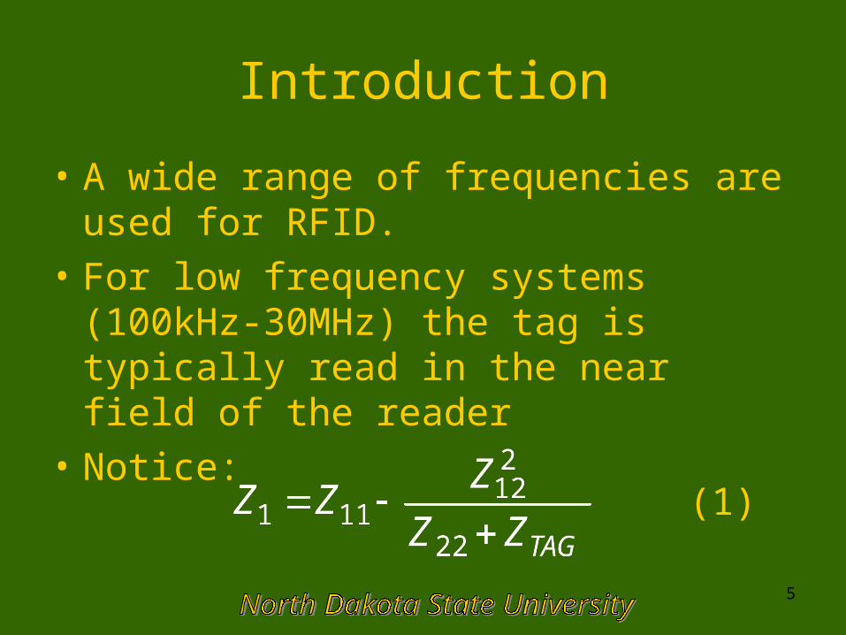
• A wide range of frequencies are used for RFID.
• For low frequency systems (100kHz-30MHz) the tag is typically read in the near field of the reader
• Notice:
(1)

6
Introduction
• Now consider the case when the reader may be in the far field.
• This is the case for high-frequency RFID systems.
• Instead of viewing the communications between the tag and the reader as radar cross section or scattering aperture [1] we consider the current induced on an antenna as a function of the impedance of the tag circuitry.

7
Introduction
• Current induced on the antenna radiates in all directions.
• This induced current changes with the terminal impedance.
• Therefore the relationship between the field at the reader and the terminal impedance can be observed.
8
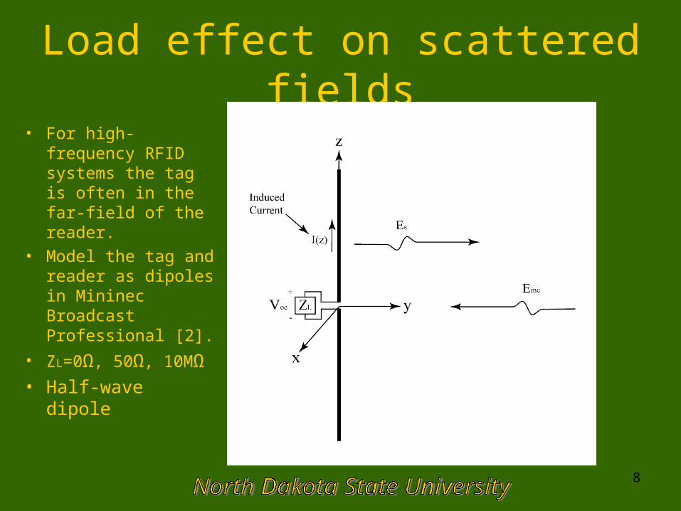
Load effect on scattered fields
• For high-frequency RFID systems the tag is often in the far-field of the reader.
• Model the tag and reader as dipoles in Mininec Broadcast Professional [2].
• ZL=0Ω, 50Ω, 10MΩ
• Half-wave dipole
9
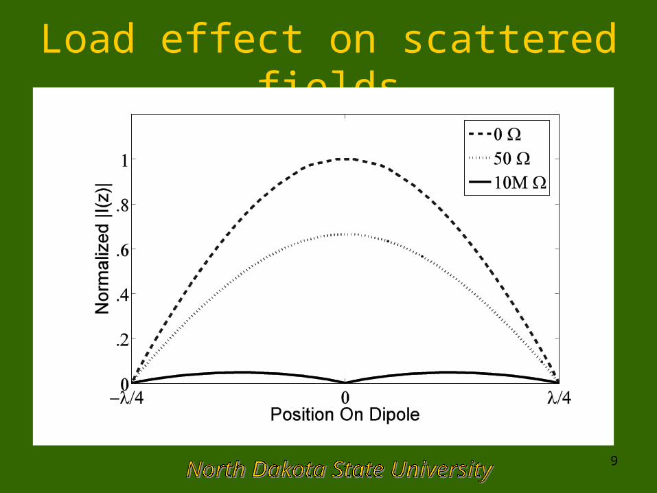
Load effect on scattered fields
10
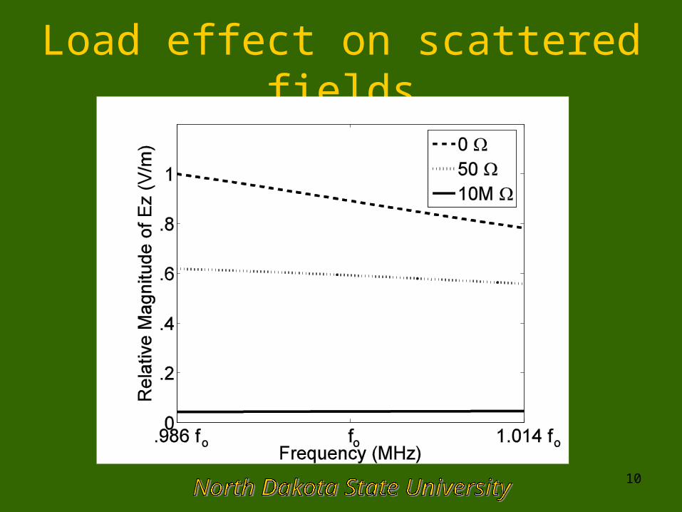
Load effect on scattered fields

11
Load effect on scattered fields
• QUICNEC (GUI) [3]-[5]: Quasi-Static Inductive Capacitive Numerical Electromagnetics Code based on MOM
• Problems can contain electrically small regions that are geometrically complex as well as full-wave regions.
• Results are compared to Mininec• The following results are for a half wave
dipole at fo.
12
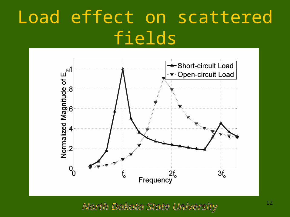
Load effect on scattered fields
13
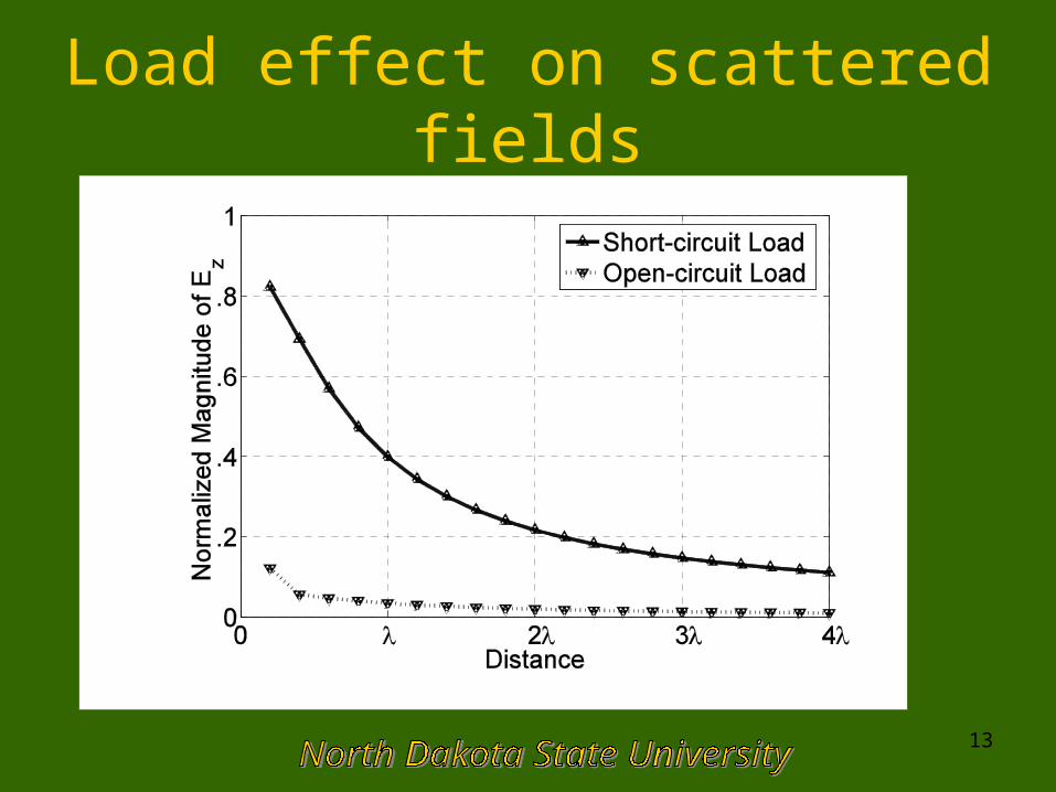
Load effect on scattered fields
14
Load effect on scattered fields
The previous results illustrate the point that the operation of passive, high-frequency RFID systems can be thought of in terms of how the induced current and resultant scattered field vary with the impedance of the tag circuitry.

15
Derivation of analytical expressions
The current distribution for a resonant dipole can be approximated as [6]:
where and is the maximum current on the antenna.
(2)
16
Derivation of analytical expressions
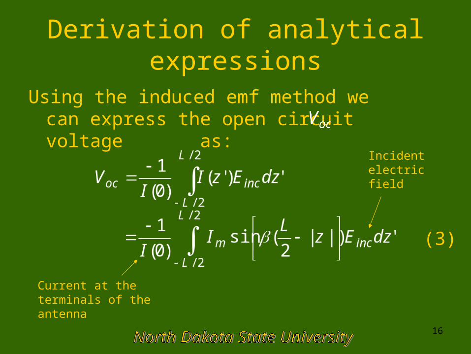
Using the induced emf method we can express the open circuit voltage as:
Current at the terminals of the antenna
Incident electricfield
(3)
17
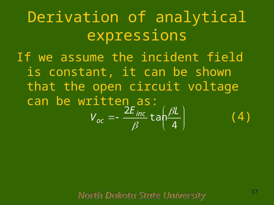
Derivation of analytical expressions
If we assume the incident field is constant, it can be shown that the open circuit voltage can be written as:
(4)

18
Derivation of analytical expressions
Using voltage division on the figure below we get [6]:
(5)

19
Derivation of analytical expressions
Substituting (4) into (5) and solving for current gives:
(6)
The previous expression gives us a representation for the maximum current on the antenna in terms of the incident field.

20
Derivation of analytical expressions
We can write the expression for the scattered field at any point in free space around the antenna by evaluating [6]:
(7)
and
where
21
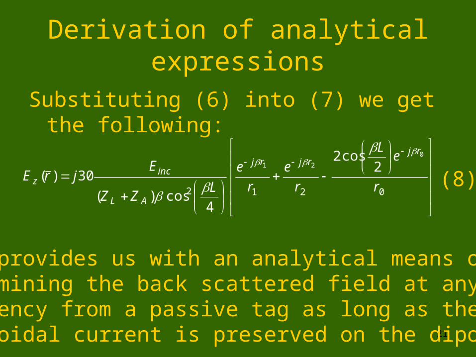
Derivation of analytical expressions
Substituting (6) into (7) we get the following:
(8)
This provides us with an analytical means of determining the back scattered field at any givenfrequency from a passive tag as long as the sinusoidal current is preserved on the dipole.

22
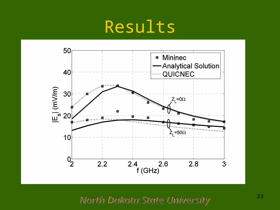
Results
To validate the previous expression the thin wire dipole to the right was evaluated with a length of .06m and a radius of 1mm. The incident field was defined at 1V/m with zero phase.
Scattered field compared to MININEC and QUICNEC at 1m.
23
Results

24
Conclusion
• Examines alternate way of viewing back scatter based communications
• We observed that the current induced on the tag antenna and the corresponding scattered field are both functions of the impedance of the tag circuitry
• Scattered field shown using two computational packages: MININEC Broadcast Professional and QUICNEC
• Closed form expressions are presented for the induced current and resulting scattered field

25
Conclusion
• (8) provides a clear relation between the scattered field and the load impedance of the dipole which can especially be used by EMC engineers.
• It should be noted, however, that the usable range of RFID systems not only depends on the magnitude of the scattered field, but also on the maximum distance the tag can harvest enough energy to turn on and communicate [7]-[9].
• Max power is harvested during conjugate match

26
Acknowledgements
• Defense Microelectronics Activity (DMEA)
• Mr. Aaron Reinholtz of the Center for Nanoscale Science and Engineering (CNSE)
• Dr. Greg McCarthy of the Center for Nanoscale Science and Engineering (CNSE)

27
References
[1] K. Finkenzeller, RFID Handbook, John Wiley and Sons, West Sussex, England 2003.
[2] J.W. Rockway and J.C. Logan, MININEC Broadcast Professional for Windows, EM Scientific, Inc. Carson City, NV, 1996.
[3] Benjamin D. Braaten, “An Integral Equation Technique for Solving Electromagnetic
Problems with Electrically Small and Electrically Large Regions,” M.S. Thesis, North Dakota State University, Fargo, N.D. 2005.

28
References
[4] R.M.Nelson, B. Braaten, and M. Mohammed, “Electric Field Integral Equations for Electromagnetic Scattering Problems with Electrically Small and Electrically Large Regions,” submitted for publication in the IEEE Transactions on Antennas and Propagation.
[5] Benjamin D. Braaten, “QUICNEC User’s Manual,” Technical Report, Dept. of
Electrical and Computer Engineering, North Dakota State University, Fargo, N.D. 2005.
29
References
[6] Constantine A. Balanis, Antenna Theory Analysis and Design, Harper and
Row, New York, 1982.
[7] K.V. Seshagiri Rao, Pavel V. Nikitin, and Sander F. Lam, “Antenna Design for UHF
RFID Tags: A Review and a Practical Application,” IEEE Transactions on Antennas and Propagation, Vol. 53, No. 12, p. 3870-3876, December 2005.

30
References
[8] Giuseppe De Vita and Giuseppe Iannaccone, “Design Criteria for the RF Section of UHF and Microwave Passive RFID Transponders,” IEEE Transactions on Microwave Theory and Techniques, Vol. 53, No. 9, p. 2978-2990, September 2005.
[9] Pavel V. Nikitin, K.V. Seshagiri Rao, Sander F. Lam, Vijay Pillai, Rene Martinez and harley Heinrish,
“Power Reflection Coefficient Analysis for Complex Impedances in RFID Tag Design,” IEEE Transactions on Microwave Theory and Techniques, Vol. 53, No. 9, p. 2721-2825, September 2005