high-energy density beams and plasmas for micro- and nano
TRANSCRIPT

High-energy density beams and plasmas for micro- and nano-texturing of surfaces by rapid
melting and solidification
This article has been downloaded from IOPscience. Please scroll down to see the full text article.
2011 J. Phys. D: Appl. Phys. 44 174026
(http://iopscience.iop.org/0022-3727/44/17/174026)
Download details:
IP Address: 128.174.163.99
The article was downloaded on 17/08/2011 at 23:40
Please note that terms and conditions apply.
View the table of contents for this issue, or go to the journal homepage for more
Home Search Collections Journals About Contact us My IOPscience
IOP PUBLISHING JOURNAL OF PHYSICS D: APPLIED PHYSICS
J. Phys. D: Appl. Phys. 44 (2011) 174026 (12pp) doi:10.1088/0022-3727/44/17/174026
High-energy density beams and plasmasfor micro- and nano-texturing of surfacesby rapid melting and solidificationVijay Surla and David Ruzic
Center for Plasma Material Interactions, Department of Nuclear, Plasma and Radiological Engineering,University of Illinois at Urbana Champaign, Urbana, IL 61801, USA
E-mail: [email protected]
Received 9 November 2010, in final form 28 February 2011Published 14 April 2011Online at stacks.iop.org/JPhysD/44/174026
AbstractSeveral advances in materials research have been made due to the wide array of tools currentlyavailable for the processing of materials: plasmas, electron beams, ion beams and lasers. Thearea of material science is fortunate to have seen the development of these tools over the years,be it for new bulk materials, coatings or for surface modification. Several applications havebenefited and many more will in the future as the properties of the materials are altered on amicro/nanoscale. Currently, several techniques exist to modify the physical, chemical andbiological properties of the material surface; however, this review limits itself to surfacemodification applications using the rapid thermal processing (RTP) technique. First, a briefoverview of the existing surface modification methods using the principles of RTP is reviewed,and then a novel method to create micro/nanostructures on the surface using pulsed plasmaexposure of materials is presented.
(Some figures in this article are in colour only in the electronic version)
1. Introduction
Materials research has been motivated to obtain bettermaterial properties than the existing materials. Researchin nanomaterials is no exception—the grain size of thesematerials being in the nanoscale has given rise to superiorproperties compared with the conventional materials. Asummary of changes in material properties due to theextremely small grain sizes in nanostructured materials isvery well detailed by Suryanarayana [1] and referencestherein. These include increased strength/hardness, enhanceddiffusivity, improved ductility/toughness, reduced density,reduced elastic modulus, higher electrical resistivity, increasedspecific heat, higher coefficient of thermal expansion, lowerthermal conductivity and superior soft magnetic properties[1]. While nanomaterials have shown tremendous opportunity,synthesizing them with reproducible properties has remainedan active engineering problem.
The development of new techniques for producing nanos-tructures is important for several engineering applications.The nanostructured materials could be synthesized either bythe ‘top-down’ processing approach where the bulk material
is modified to produce nanostructures on the surface, or the‘bottom-up approach’ in which nanostructures are assembledfrom building blocks such as atoms, ions or molecules. Pro-cessing techniques such as sputtering, laser ablation and depo-sition schemes fall under the bottom-up approach. Top-downprocessing includes techniques such as rapid surface melting,rapid solidification processing (RSP), surface nanostructuring,etc. A very good review of papers producing nanocrystallinematerials is already provided in a number of references [2–9] and this review will not cover those methods. Also, tech-niques involving severe plastic deformation methods have beensuccessfully used in the formation of nanocrystalline surfacelayers in various metallic materials, as demonstrated in Satoaet al and references therein [10]. There is an abundant amountof research in nanomaterials that is available in the literatureand it is beyond the scope of this review to cover all of them.Instead, what this review includes is the methods used to pro-duce nanostructures based on rapid thermal processing (RTP)techniques.
The RTP of materials has been widely used in themicroelectronics industry in the past for annealing of wafersand improving their properties [11]. Dynamic control
0022-3727/11/174026+12$33.00 1 © 2011 IOP Publishing Ltd Printed in the UK & the USA
J. Phys. D: Appl. Phys. 44 (2011) 174026 V Surla and D Ruzic
of temperature is achieved in the RTP technique, whichpermits high heating and cooling rates that cannot be reachedwith conventional treatments. In recent years, RTP hasbeen increasingly applied to the processing of materials fordifferent applications. The controllable heating profiles allowstructuring of material surfaces via expediting phase transitionsand tailoring materials morphology.
Recently, the rapid rise of research and development inplasmas and lasers has seen the use of these tools for RTP.Electron beams, ion beams, lasers and plasmas have all beensuccessfully used in the past for improving material propertiesand a review is provided in section 2. In addition, a novelpulsed plasma source which was originally developed for itsuse in extreme ultraviolet (EUV) lithography is used to tailorthe surface properties in the micro/nanoscale, and the resultsare presented in section 3. Finally, a summary is provided insection 4.
2. The RTP technique
RTP is usually understood to be a semiconductor processingmethod, as this process dates back to the late 1960s [12],when IBM pioneered making submicrometre features usingpulsed laser irradiation [13]. RTP is a tool that enables rapidthermal cycles which cannot be performed with conventionalbatch furnaces. The conventional furnace processing placesa limitation on the maximum heating and cooling rates tofew hundreds of K min−1 and the processing time to severalminutes. These restrictions are imposed by the high thermalmass of the system as well as the way the energy is transferredto the wafers. RTP, owing to its low thermal mass, enableshigh temperature gradients and faster processing times.
While RTP was dominated by laser processing in the earlyyears, the later years saw a rapid rise in the use of other heatingsources. A good review of heating sources for RTP systemsis covered in [12]. Any process that involves fast heating andcooling rates could be placed in this category. Review papers[14–16] described the advantages of isothermal heating (lamp,resistance, and e-beam heating, 1–100 s processing time) overthermal flux (scanned continuous wave (cw) laser, e-beam,0.1–10 ms processing time) and adiabatic heating (pulsedbeam or laser, 1–1000 ns processing time) to semiconductormanufacturing [17, 18]. However, the demands of RTPsystems for material modification are quite different from thoseused in microelectronics applications. For material processing,the RTP technique involves rapid melting of the surface of amaterial followed by rapid quenching due to heat conductioninto the unaffected bulk material. These require higher heatingand cooling rates and so adiabatic heating presents an ideal RTPmethod for micro/nanostructuring of surfaces.
Increasing applications of RTP processing in materialsprocessing, especially for producing micro- or nanostructures,has been seen in recent years. A good review of the RTPtechnique for its application in magnetic materials is covered in[19]. Several reviews relating to this subject are also availablein the name of RSP, given by Suryanarayana [18], Jacobson[20] and references therein. The tools that are available tomeet the needs of material modification are lasers, e-beams,
ion beams and pulsed plasmas, and therefore these are coveredin detail in this review.
2.1. RTP processing using electron beams
The use of electron beams over the years has increasedtremendously and is now a commercial technology for severalapplications. For example, electron beams are increasinglyused in manufacturing applications such as drilling, melting,welding, etc. In addition, electron beams, due to the wide rangeof possible energies, have also been used in material processingapplications that include electron-beam processing, electron-beam texturing and sterilization applications. Recently, therehas been an increased growth of their use in semiconductormanufacturing, as well as in deposition and lithographyapplications. In the view of nano-material processing, e-beamshave been used in nanostructuring of materials using e-beamlithography [21] and also using e-beam deposition [22].However, in this review, because the variants of RTP are beingsurveyed, we limit ourselves to the use of electron beams formaterial processing where the intense energy of the e-beamis deposited into a thin layer of bulk material in a short time,such that the structure of the surface is altered. It is possibleto develop unique phases, and surface compositions throughthe appropriate combination of e-beam processing parameters.This results in the formation of either micro- or nanostructuresthat will significantly enhance the properties of the surface.
The structuring of material surfaces by the use of e-beamshas been reported in the literature with different names, forexample as the rapid quenching process, electron-beam surfacemelting process, electron-beam hardening process, etc. Thesesurface structures are expected to improve properties such ashardness, wear, erosion and corrosion resistance.
Electron-beam rapid quenching involves the rapidinteraction of material with an electron beam yielding a thinmelt layer on the surface. During this rapid surface meltingprocess, a certain amount of thermal energy is conducted tothe bulk giving rise to a steep temperature gradient between thesolid (bulk) and the liquid (melt). This gradient results in rapidsolidification. The quench rate is mainly dependent on processparameters such as the beam power, traverse speed and theinteraction time. As a result of high cooling rates, interestingmetallurgical structures are produced on the surface. Mawellaand Honeycombe [23] investigated the properties of an ultra-high-strength alloy steel after e-beam treatment and showedthat the rapid quenching process leads to a high degree of grainrefinement and an increase in solid solubility which, in turn,increases the amount of retained austenite. The lowering ofmartensite transformation temperature due to the high coolingrate and the increased solid solubility favour the formationof twinned martensite. The considerable increase in themicrohardness of the rapidly quenched layer, with respect tothat of the solid state quenched steel, is attributed to interlinkedphenomena such as austenite grain refinement, the increasedsolubility and the martensitic structure [23].
In the electron-beam surface melting process, a surfacelayer is fused by means of an electron beam and resolidifiedquickly. The rapid solidification yields improvement in the
2
J. Phys. D: Appl. Phys. 44 (2011) 174026 V Surla and D Ruzic
microstructure and increases the hardness of the remeltedlayers. Petrov [24] reported changes in the structuralmorphology of aluminium alloys in the electron-beam treatedzones and also an increase in hardness as a result of surfacedoping. Markov et al [25] demonstrated the hardening andtempering zones in quenched U7A steel irradiated with apulsed electron beam.
In the electron-beam hardening process, the heatgenerated by the e-beam impingement on the surface isused to transform the material phase, which is due to rapidconduction of heat into the relatively cold bulk interior ofthe material. Dimitrov et al [26] studied the electron-beamtreatment of ion nitriding steel and found that the hardnessincreased. The high hardness is attributed to the refinedstructure consisting of a-solid solution (nitrous martensite)and y-solid solution (nitrous austenite) and dispersed finenitride precipitations. They also reported an increase inwear resistance of the electron-beam treated layer, which istwice that of the ion nitrided specimen. Song et al [27, 28]investigated the effects of electron-beam surface hardeningtreatment on the microstructure and hardness of AISI D3tool steel and showed that the microstructure of the hardenedlayer consisted of martensite, a dispersion of fine carbides andretained austenite, while the transition area mainly consistedof tempered sorbite. Also, the microhardness of the hardenedlayer on the surface increased dramatically compared with thatof base material. The e-beam method has successfully beenapplied to the treatment of alloys as well. For example, Nagaeet al [29] demonstrated the improvement in surface roughnessand hardness of a Co–Cr–Mo alloy.
In the following years, several researchers reported theformation of new structures resulting in the improvement ofseveral material properties under the same surface treatmentmethod. In all these methods, pulsed electron beams areused to modify materials by depositing energy in them.To effectively change the surface of a material, the mainrequirement is that the beam energy must be dissipatedadiabatically in a thin layer of bulk material in a short time.A pulsed electron beam capable of melting the surface layerof any material into depths of a few tens of µm at a rateof 106–109 K s−1 is used to achieve the desired structuralconditions. The structures produced in this process are veryfine grained down to nanometre size and sometimes existin metastable phases. It is preferable to heat the treatedlayer without marked evaporation and boiling of the meltedphase, and also without significant energy loss due to thermalconductivity inside the bulk material, which is the adiabaticmode of RTP.
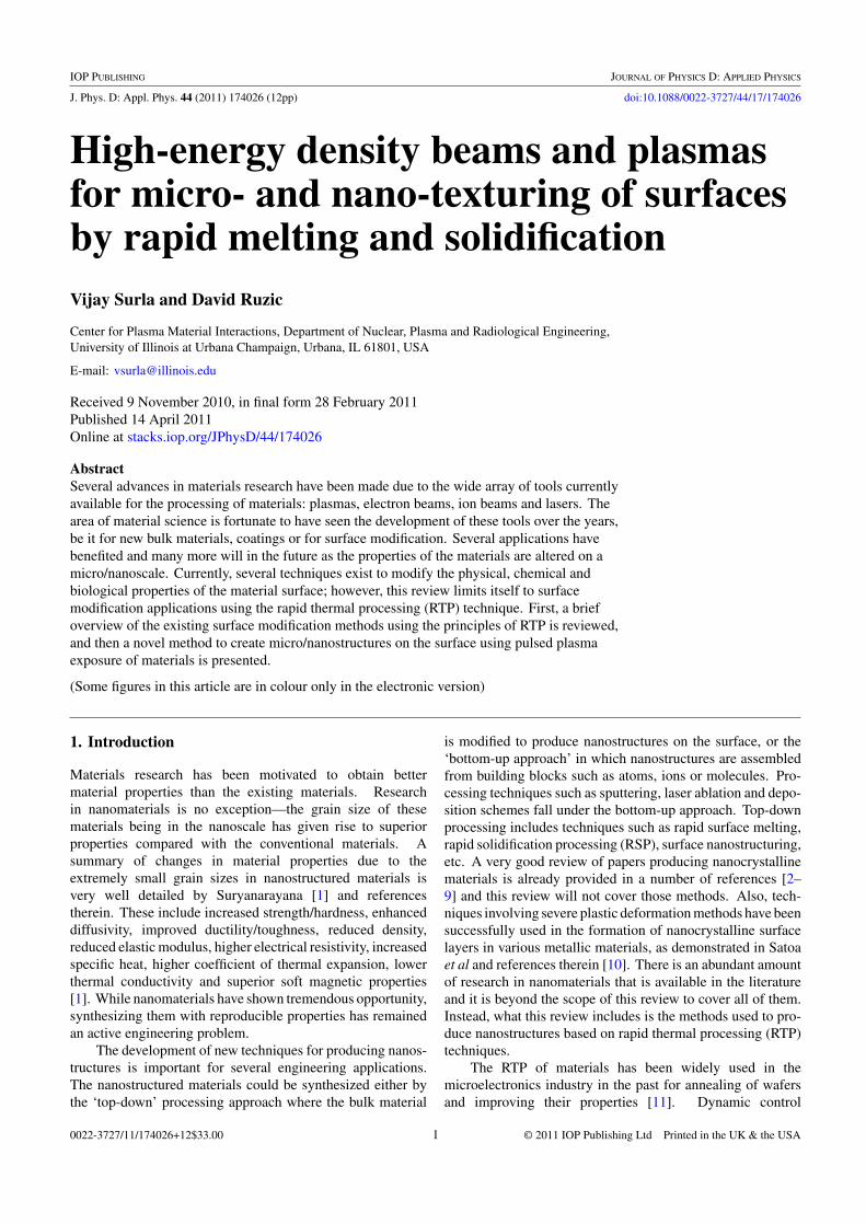
The pulsed electron-beam facilities GESA I and GESA IIwere developed in cooperation between the Efremov InstituteSt Petersburg, Russia, and the Research Center Karlsruhe(FZK), Germany, for large area surface treatment [30].The two facilities use the same principal set-up as detailedin [31]: electron injector of triode type with a multipointexplosive emission cathode, transport channel, treatmentchamber, magnetic system, high-voltage generator, pulse-duration control unit (PDCU), vacuum system, control rack,radiation protection and mechanical support. A schematic of
Figure 1. Schematic of the GESA pulsed electron-beam facility.Electron-beam parameters are electron energy: 50–400 keV, energydensity : ∼6 MW cm−2, pulse duration (controllable): 1–40 µs andbeam diameter: 5–10 cm [31].
the GESA facility and its capabilities are shown in figure 1,which is typical of such large scale facilities designed todo RTP with electron beams. Recently, Weisenburger [31]presented the surface modification materials using the abovefacilities and reported that the changes in microstructure ledto hardening of gears and increased their wear resistance. Adecrease in the oxidation rate of high temperature alloys is alsoreported. For more details, readers are directed to referencesin [31] as they cover a range of applications from gears in theautomotive industry, turbine blades for energy, cutting toolsfor manufacturing, to implants and surgical tools in medicineapplications.
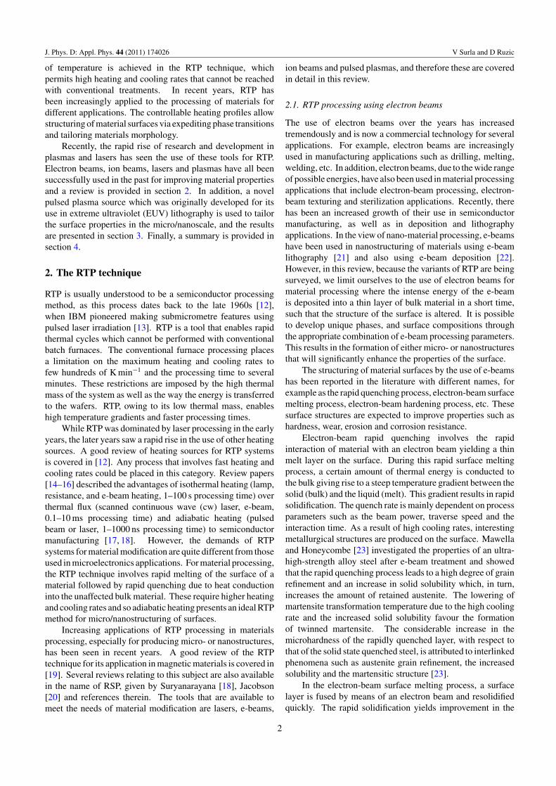
Hao and Dong [32] demonstrated the use of high currentpulsed electron beams (HCPEBs) for surface modification ofmetallic materials. Their group has actively been studyingthe HCPEB treatment of pure metals and alloys, such asaluminium and carbon steels [33–38]. A high efficient electronbeam of low-energy (10–40 keV), high peak current (102–103 A cm−2), with short pulse duration (5 ms) is typicallyused to generate power density up to 108–109 W m−2 at thetarget surface. Recently, the same group has reported theformation of nanostructures on carbon steel using HCPEB [36]with the following beam parameters: electron energy 25 kV,pulse duration 3.5 µs and energy density 4 J cm−2, as shownin figure 2. After e-beam treatment, it is found that themodified surface layer can be divided into three zones: themelted layer of depth 3 to 10 µm, the heat and stress effectingzone (10 µm below to about 250 µm) and matrix, where ananostructure and/or amorphous layer is formed in the near-surface region [36].
Ivanov et al reported the use of low-energy highcurrent electron-beam (LEHCEB) sources as a promisingway of developing new highly efficient techniques for thesurface treatment of material [39–42]. Proskurovsky [41]showed that for a variety of constructional and tool materialsincluding carbon steel, stainless steel, aluminium alloys,titanium alloys and hard alloys, the surface layers modifiedas a result of melt quenching show improved strength and
3

J. Phys. D: Appl. Phys. 44 (2011) 174026 V Surla and D Ruzic
Figure 2. TEM image showing the nanostructure of carbonsteel [36].
electrochemical properties. Recently, Koval and Ivanovstudied metalloceramic and ceramic materials by electron-beam treatment and observed the formation of submicro-and nanocrystalline multi-phase structures, that result in anincrease in physico-mechanical and tribological characteristicsof the treated material [42]. Also, recently, Mohanty et al [43]demonstrated polyaniline nanowires formation by electron-beam processing of polyaniline thin films for applications inpolymer nanomaterials.
Korenev et al demonstrated the design and development ofpulsed low-energy electron sources for material modificationapplications [44]. New designs aimed at industrial scalematerial modification technologies are required. Pulsedelectron beams for this technology must have a large crosssection and good current density uniformity [44].
In summary, the use of electron beams in the surfacemodification of materials is being actively pursued by severalgroups for different applications as can be found in the providedreferences. A variety of e-beam sources were used to treat awide range of metallic materials and alloys. An improvementin the properties is shown due to the formation of resultingmicrostructures due to the e-beam treatment. Recently, theuse of e-beams for nanostructuring was also demonstrated andit includes even polymer nanomaterials.
2.2. RTP processing using laser beams
Surface modification using lasers also involves melting of thematerial that interacts with the laser beam followed by thesolidification of this molten material. During the cooling cycle(i.e. after the laser irradiation time is over), the solidificationof the molten material leads to the formation of differentmicrostructural features depending on several factors suchas cooling rate and laser fluence, and while it is possible toproduce nanocrystalline thin films using PVD techniques orlaser ablation, as demonstrated in [44–48], this review focusis on RTP induced changes in producing the desired micro- ornanostructure on the surface.
The applications of lasers are very widely known and itis beyond the scope of this paper to cover the entire spectrum.Limiting ourselves to the processing of materials, lasers havebeen the first tool of choice since its invention. Both cw andpulsed lasers have been used for producing microstructuresthat slowly led the way to producing nanostructures as well.Strutt et al [49] demonstrated the laser surface melting of
Figure 3. Schematic of the laser surface modification set-up used byHarimkar [61]. Parameters: Nd–YAG laser beam (1064 nm),fluence: 458–687 J cm−2 and linear scan speed: 100 cm min−1.
high speed tool steels using a continuous CO2 laser beam,producing the microstructures that resulted in an appreciableincrease in hardness. McCafferty et al [50] demonstrated theuse of pulsed laser beams for rapid solidification and meltingof an aluminium alloy sample in order to modify the near-surface microstructure, the surface chemistry and the surfacetopography. The use of pulsed lasers allows the rapid meltingof a thin surface layer which is then rapidly solidified, with thebulk providing self-quenching when the incident radiation isremoved. This allows greater control in producing the desiredmicrostructures. The RTP processing using laser beams onproducing microstructures is similar to the use of e-beams andseveral research groups [51–63] have obtained microstructureson different kinds of materials (metals, alloys, ceramics)for several applications, including automotive manufacturing,biological, optical and magnetic materials. A schematic of thetypical experimental set-up for microstructuring with lasers isgiven in figure 3. Typically, a laser beam (here, a 4 kW cwNd : YAG laser (λ = 1064 nm) beam) is focused on to thetarget surface (alumina ceramic sample (5 × 5 × 2.5 cm) as infigure 3). The target may be mounted on a translation stagethat is controlled by CNC programs, allowing precise controlof the movements along the X-, Y - and Z-axes. The scan speedand laser fluence are selected appropriately.
The logical progression of the use of lasers is for its use inthe production of nanostructures, which is more challenging.The rapid progress in the development of ultra-fast lasersbrought life to researchers in material processing applications.The femtosecond lasers have been used for producingnanostructures by (bottom-up approach) laser deposition[46–48] and by (top-down approach) surface nanostructuringof solids [64–68]. Nolte et al [64] and Chimmalgi et al [65]used femtosecond laser pulses in combination with scanningnear field optical microscopes or atomic force microscopes toproduce nanostructures. Koch et al [66] presented fabricationof nanojets on thin gold films, as shown in figure 4, using acommercial 1 kHz femtosecond laser system delivering 0.9 mJ,30 fs laser pulses at 800 nm. This work is typical of thenanostructuring that is possible with such techniques.
4
J. Phys. D: Appl. Phys. 44 (2011) 174026 V Surla and D Ruzic
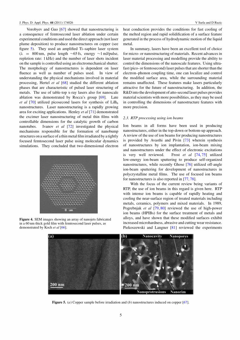
Vorobyev and Guo [67] showed that nanostructuring isa consequence of femtosecond laser ablation under certainexperimental conditions and used the direct approach (not laserplume deposition) to produce nanostructures on copper (seefigure 5). They used an amplified Ti–saphire laser system(λ = 800 nm, pulse length ∼65 fs, energy ∼1 mJ/pulse,repletion rate: 1 kHz) and the number of laser shots incidenton the sample is controlled using an electromechanical shutter.The morphology of nanostructures is dependent on laserfluence as well as number of pulses used. In view ofunderstanding the physical mechanisms involved in materialprocessing, Hertel et al [68] studied the different ablationphases that are characteristic of pulsed laser structuring ofmetals. The use of table-top x-ray lasers also for nanoscaleablation was demonstrated by Rocca’s group [69]. Lateet al [70] utilized picosecond lasers for synthesis of LiB6
nanostructures. Laser nanostructuring is a rapidly growingarea for exciting applications. Henley et al [71] demonstratedthe excimer laser nanostructuring of metal thin films withcontrollable dimensions for the catalytic growth of carbonnanotubes. Ivanov et al [72] investigated the physicalmechanisms responsible for the formation of nanobumpstructures on a surface of a thin metal film irradiated by a tightlyfocused femtosecond laser pulse using molecular dynamicssimulations. They concluded that two-dimensional electron
Figure 4. SEM images showing an array of nanojets fabricatedin a 60 nm thick gold film with femtosecond laser pulses, asdemonstrated by Koch et al [66].
Figure 5. (a) Copper sample before irradiation and (b) nanostructures induced on copper [67].
heat conduction provides the conditions for fast cooling ofthe melted region and rapid solidification of a surface featuregenerated in the process of hydrodynamic motion of the liquidmetal.
In summary, lasers have been an excellent tool of choicefor micro- or nanostructuring of materials. Recent advances inlaser material processing and modelling provide the ability tocontrol the dimensions of the nanoscale features. Using ultra-fast (pico- or femtosecond) laser pulses that are shorter than theelectron–phonon coupling time, one can localize and controlthe modified surface area, while the surrounding materialremains unaffected. These features make lasers particularlyattractive for the future of nanostructuring. In addition, theR&D into the development of atto-second laser pulses providesmaterial scientists with more possibilities, as they may be usedin controlling the dimensions of nanostructure features withmore precision.
2.3. RTP processing using ion beams
Ion beams in all forms have been used in producingnanostructures, either in the top-down or bottom-up approach.A review of the use of ion beams for producing nanostructuresis provided by Avasthi and Pivin [73] wherein synthesisof nanostructures by ion implantation, ion-beam mixingand nanostructures under the effect of electronic excitationsis very well reviewed. Frost et al [74, 75] utilizedlow-energy ion-beam sputtering to produce self-organizednanostructures, while recently Ghose [76] utilized off-angleion-beam sputtering for development of nanostructures inpolycrystalline metal films. The use of focused ion beamsfor nanostructures is also reported in [77, 78].
With the focus of the current review being variants ofRTP, the use of ion beams in this regard is given here. RTPwith intense ion beams is capable of rapidly heating andcooling the near-surface region of treated materials includingmetals, ceramics, polymers and mixed materials. In 1989,Pogrebnjak et al [79, 80] reviewed the use of high-powerion beams (HPIBs) for the surface treatment of metals andalloys, and have shown that these modified surfaces exhibitincreased microhardness, abrasive and cutting wear resistance.Piekoszewski and Langner [81] reviewed the experiments
5
J. Phys. D: Appl. Phys. 44 (2011) 174026 V Surla and D Ruzic
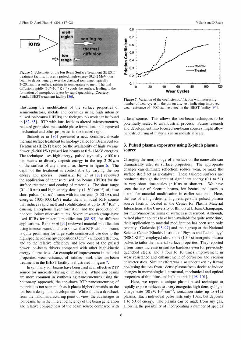
Figure 6. Schematic of the Ion Beam Surface Treatment (IBEST)treatment facility. It uses a pulsed, high-energy (0.2–2 MeV) ionbeam to deposit energy over the classical ion range, typically2–20 µm, in a surface, raising its temperature to melt. Thermaldiffusion rapidly (109–1010 K s−1) cools the surface, leading to theformation of amorphous layers by rapid quenching. Courtesy:Sandia IBEST treatment facility [86].
illustrating the modification of the surface properties ofsemiconductors, metals and ceramics using high intensitypulsed ion beams (HIPIBs) and their group’s work can be foundin [82–85]. RTP with ions leads to altered microstructures,reduced grain size, metastable phase formation, and improvedmechanical and other properties in the treated region.
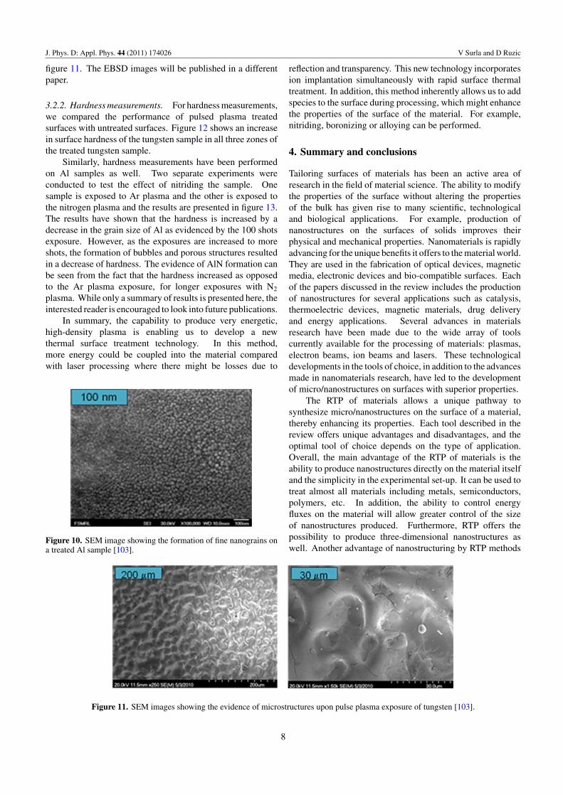
Stinnett et al [86] presented a new, commercial-scalethermal surface treatment technology called Ion Beam SurfaceTreatment (IBEST) based on the availability of high averagepower (5–500 kW) pulsed ion beams at 0.5–1 MeV energies.The technique uses high-energy, pulsed (typically <100 ns)ion beams to directly deposit energy in the top 2–20 µmof the surface of any material as shown in figure 6. Thedepth of the treatment is controllable by varying the ionenergy and species. Similarly, Rej et al [87] reviewedthe application of intense pulsed ion beams (IPIBs) for thesurface treatment and coating of materials. The short range(0.1–10 µm) and high-energy density (1–50 J cm−2) of theseshort-pulsed (<1 µs) beams with ion currents (5–50 kA), andenergies (100–1000 keV) make them an ideal RTP sourcethat induces rapid melt and solidification at up to 1010 K s−1,causing amorphous layer formation and the production ofnonequilibrium microstructures. Several research groups haveused IPIBs for material modification [88–93] for differentapplications. Renk et al [94] reviewed material modificationusing intense beams and have shown that RTP with ion beamsis quite promising for large scale commercial use due to thehigh specific ion energy deposition (J cm−3) without reflection,and to the relative efficiency and low cost of the pulsedpower ion-beam drivers compared with other high-kineticenergy alternatives. An example of improvement in materialproperties, wear resistance of stainless steel, after ion-beamtreatment in the IBEST facility is illustrated in figure 7.
In summary, ion beams have been used as an effective RTPsource for microstructuring of materials. While ion beamsare more common in synthesizing nanostructures using thebottom-up approach, the top-down RTP nanostructuring ofmaterials is not seen much as it places higher demands on theion-beam design and development. While this is a drawbackfrom the nanomanufacturing point of view, the advantages inion beams lie in the inherent efficiency of the beam generationand relative compactness of the beam source compared with
Figure 7. Variation of the coefficient of friction with increasingnumber of wear cycles in the pin on disc test, indicating improvedwear resistance of 440C stainless steel in the IBEST facility [94].
a laser source. This allows the ion-beam techniques to bepotentially scaled to an industrial process. Future researchand development into focused ion-beam sources might allownanostructuring of materials in an industrial scale.
3. Pulsed plasma exposures using Z-pinch plasmasource
Changing the morphology of a surface on the nanoscale candramatically alter its surface properties. The appropriatechanges can eliminate reflection, reduce wear, or make thesurface itself act as a catalyst. These tailored surfaces areproduced through the input of significant energy (0.1 to 5 J)in very short time-scales (∼10 ns or shorter). We haveseen the use of electron beams, ion beams and lasers asa tool for material modification in earlier sections. Here,the use of a high-density, high-charge-state pulsed plasmasource facility, located in the Center for Plasma MaterialInteractions at the University of Illinois at Urbana Champaign,for micro/nanostructuring of surfaces is described. Although,pulsed plasma sources have been available for quite some time,their application to material modification has been seen onlyrecently. Garkusha [95–97] and their group at the NationalScience Center ‘Kharkiv Institute of Physics and Technology’(NSC KIPT) employed ultra-short (10−6 s) energetic plasmapulses to tailor the material surface properties. They reporteda four times increase in surface hardness even for previouslyquenched steels, and a four to 10 times improvement inwear resistance and enhancement of corrosion and erosioncharacteristics. Similar effort was also undertaken by Rawatet al using the ions from a dense plasma focus device to inducechanges in morphological, structural, mechanical and opticalproperties of thin films and bulk materials [98–101].
Here, we report a unique plasma-based technique torapidly expose surfaces to a very energetic, high-density, high-charge-state (30 eV, 1020 cm−3, ionization states up to +12)plasma. Each individual pulse lasts only 10 ns, but deposits1 to 5 J of energy. The plasma can be made from any gas,allowing the possibility of incorporating a number of species
6

J. Phys. D: Appl. Phys. 44 (2011) 174026 V Surla and D Ruzic
Figure 8. Schematic (a) and photograph (b) of the XTS 13-35 EUV Z-Pinch at the University of Illinois. The device is capable of operationup to 1.5 kHz, 8 J per 10 ns pulse. The pinch rapidly expands so energy density can be controlled through sample placement.
Figure 9. Schematic of the experimental set-up for micro/nanotexturing of surfaces.
into the material being treated. The high-density high-charge-state pulsed plasma source is a source of energetic ions, neutralsand photons, which are all responsible for depositing energyinto a thin layer of any surface. The depth of modificationand the resultant microstructure is controlled by the plasmaparameters. The rapid quenching due to the bulk materialproduces a fine grained layer containing microstructures ornanostructures that exhibit superior material properties. Thistechnology could be used for any material including ceramics,metals or polymers.
3.1. Experimental set-up
Figure 8 shows the discharge-produced plasma source. It is aZ-pinch used as a source for EUV lithography. We are the firstto intentionally use this plasma to modify material surfaces.The plasma produces bursts of EUV (13.5 nm) light, but only3% or less of the energy goes into such photons. The rest goesinto plasma creation of energetic ions, electrons and a widerange of photon energies [102] that are all utilized here forsurface tailoring.
Figure 9 shows the schematic of the experimental set-up.A sample is loaded using a load lock and transfer arm and inthe current set-up the sample is positioned at approximately2 cm away from the Z-pinch plasma. The energy densityon the target can be controlled through this target sample
placement. Several diagnostics were used to characterize theplasma source and are not covered here as it is not the subject ofthe review. The proof-of-concept experiments were performedon aluminium and tungsten samples. The sample preparationprocedure and analysis can be found in [103].
3.2. Results
3.2.1. Evidence of micro/nanostructures. The idea behindmodifying the surface grain structure with a high-powerpulse is to suppress nucleation of crystalline phases, so thatan amorphous surface structure results momentarily. Thisrequires extremely rapid cooling rates to bring the temperaturedown below the glass transition level, before the onset ofcrystal nucleation. At the right energy level, nanocrystallinestructures are created. Samples of aluminium and tungstenwere treated with the Z-pinch plasma source in the XCEEDfacility and SEM images show a clear evidence of formation ofnonequilibrium microstructures consisting of nanocrystallineand/or metastable phases. Figure 10 shows the SEM imagesof an aluminium sample exposed to N2 pinch plasma for 500pulses, where in fine nanograins on the surface can be seen.Figure 11 shows the SEM image of a treated tungsten samplewhich was exposed for 45 s to the argon plasma at 50 Hzoperation, for a longer time compared with the Al sample.The resultant formation of microstructures can be seen from
7
J. Phys. D: Appl. Phys. 44 (2011) 174026 V Surla and D Ruzic
figure 11. The EBSD images will be published in a differentpaper.
3.2.2. Hardness measurements. For hardness measurements,we compared the performance of pulsed plasma treatedsurfaces with untreated surfaces. Figure 12 shows an increasein surface hardness of the tungsten sample in all three zones ofthe treated tungsten sample.
Similarly, hardness measurements have been performedon Al samples as well. Two separate experiments wereconducted to test the effect of nitriding the sample. Onesample is exposed to Ar plasma and the other is exposed tothe nitrogen plasma and the results are presented in figure 13.The results have shown that the hardness is increased by adecrease in the grain size of Al as evidenced by the 100 shotsexposure. However, as the exposures are increased to moreshots, the formation of bubbles and porous structures resultedin a decrease of hardness. The evidence of AlN formation canbe seen from the fact that the hardness increased as opposedto the Ar plasma exposure, for longer exposures with N2
plasma. While only a summary of results is presented here, theinterested reader is encouraged to look into future publications.
In summary, the capability to produce very energetic,high-density plasma is enabling us to develop a newthermal surface treatment technology. In this method,more energy could be coupled into the material comparedwith laser processing where there might be losses due to
Figure 10. SEM image showing the formation of fine nanograins ona treated Al sample [103].
Figure 11. SEM images showing the evidence of microstructures upon pulse plasma exposure of tungsten [103].
reflection and transparency. This new technology incorporatesion implantation simultaneously with rapid surface thermaltreatment. In addition, this method inherently allows us to addspecies to the surface during processing, which might enhancethe properties of the surface of the material. For example,nitriding, boronizing or alloying can be performed.
4. Summary and conclusions
Tailoring surfaces of materials has been an active area ofresearch in the field of material science. The ability to modifythe properties of the surface without altering the propertiesof the bulk has given rise to many scientific, technologicaland biological applications. For example, production ofnanostructures on the surfaces of solids improves theirphysical and mechanical properties. Nanomaterials is rapidlyadvancing for the unique benefits it offers to the material world.They are used in the fabrication of optical devices, magneticmedia, electronic devices and bio-compatible surfaces. Eachof the papers discussed in the review includes the productionof nanostructures for several applications such as catalysis,thermoelectric devices, magnetic materials, drug deliveryand energy applications. Several advances in materialsresearch have been made due to the wide array of toolscurrently available for the processing of materials: plasmas,electron beams, ion beams and lasers. These technologicaldevelopments in the tools of choice, in addition to the advancesmade in nanomaterials research, have led to the developmentof micro/nanostructures on surfaces with superior properties.
The RTP of materials allows a unique pathway tosynthesize micro/nanostructures on the surface of a material,thereby enhancing its properties. Each tool described in thereview offers unique advantages and disadvantages, and theoptimal tool of choice depends on the type of application.Overall, the main advantage of the RTP of materials is theability to produce nanostructures directly on the material itselfand the simplicity in the experimental set-up. It can be used totreat almost all materials including metals, semiconductors,polymers, etc. In addition, the ability to control energyfluxes on the material will allow greater control of the sizeof nanostructures produced. Furthermore, RTP offers thepossibility to produce three-dimensional nanostructures aswell. Another advantage of nanostructuring by RTP methods
8

J. Phys. D: Appl. Phys. 44 (2011) 174026 V Surla and D Ruzic
Figure 12. Hardness measurements of distinct zones formed on atreated tungsten sample. The VHN of the unexposed tungstensample surface is 312 ± 8, which shows an increase in surfacehardness of the treated sample [103].
Figure 13. Hardness measurements of an un-annealed Al samplewhen exposed to argon (squares) and nitrogen plasma (diamonds) asthe number of exposures is varied [103]. The VHN of an annealedsample is shown for reference (triangles).
is the ability to modify material without significant loss ofmaterial, thus making it effective and a commercially viableprocess.
Of particular mention is the additional advantage thatplasmas provide to fabricate nanostructures as presented insection 3. The use of energetic and highly dense plasmaoffers efficient coupling of energy into the material comparedwith other RTP methods. In addition, plasma makes useof the energetic ions and incorporates ion implantationsimultaneously with rapid surface thermal treatment. Thisalso eliminates the need for the additional annealing methodsrequired to improve the properties of nanostructures. Also,the properties of the surface of the material can be furtherenhanced by adding dopant-like species, which can be doneinherently with the plasma processing method describedhere. The advantages of ion-beam rapid thermal processingcombined with a material alloying capability make pulsedplasma sources an attractive technology for future surfacetreatment applications.
However, careful control is required to fabricate thesenanostructures with a high degree of control over theirsize, shape and composition distributions. Optimizing thisparameter space is extremely challenging, considering thatthese nanostructures have to be produced in large scalespecifically tailored for a particular application. Hence, inorder to realize the full potential of these processing methodsmore research and development is needed to fabricate thesestructures at cost-effective production suitable for industrial
implementation. The research should include understandingthe effect of the parameters (such as energy required, pulseduration, etc) of the RTP sources on material surface usingsurface characterization techniques. As these relations are wellestablished, new cost-effective sources could be developed forthe commercial fabrication of unique nanostructures on anymaterial surface.
References
[1] Suryanarayana C 2002 The structure and properties ofnanocrystalline materials: issues and concerns JOM54 24–7
[2] Gleiter H 1989 Nanocrystalline materials Prog. Mater. Sci.33 223–315
[3] Suryanarayana C and Koch C C 2000 Nanocrystallinematerials—current research and future directionsHyperfine Interact. 130 5–44
[4] Kostya Ostrikov 2007 Plasma nanoscience: from nature’smastery to deterministic plasma-aided nanofabricationIEEE Trans. Plasma Sci. 35 127–36
[5] Ostrikov K 2005 Colloquium: Reactive plasma as a versatilenanofabrication tool Rev. Mod. Phys. 77 489–511
[6] Mariotti D and Ostrikov K 2009 Tailoring microplasmananofabrication: from nanostructures to nanoarchitecturesJ. Phys. D: Appl. Phys. 42 092002–5
[7] Ostrikov K and Murphy A B 2007 Plasma-aidednanofabrication: where is the cutting edge? J. Phys. D:Appl. Phys. 40 2223
[8] Diegoli S, Hamlett C A E, Leigh S J, Mendes P M andPreece J A 2007 Engineering nanostructures at surfacesusing nanolithography Proc. I MechE, Part G J. AerospaceEng. 221 589–629
[9] Koch C C 2003 Top down Synthesis of nanostructuredmaterials: mechanical and thermal processing methodsRev. Adv. Mater. Sci. 5 91–9
[10] Satoa M, Tsuji N, Minamino Y and Koizumi Y 2004Formation of nanocrystalline surface layers in variousmetallic materials by near surface severe plasticdeformation Sci. Technol. Adv. Mater. 5 145–52
[11] Hartt M J and Evans A G R 1988 Rapid thermal processing insemiconductor technology Semicond. Sci. Technol.3 421–36
[12] Roozeboom F and Parekh N 1990 Rapid thermal processingsystems: a review with emphasis on temperature controlJ. Vac. Sci. Technol. B 8 1249
[13] Fairfield J M and Schwuttke G H 1968 Solid State Electron.11 1175
[14] Powell R A and Manion M L 1986 Mater. Res. Soc. Symp.Proc. 52 441
[15] Singh R 1988 J. Appl. Phys. 63 R59 and references therein[16] Hill C, Jones S and Boys D 1989 NATO ASl Ser. B 207 143[17] Cullis A G 1985 Transient annealing of semiconductors by
laser, electron beam and radiant heating techniques Rep.Prog. Phys. 48 1155–233
[18] Suryanarayana C 2002 Rapid solidification processingEncyclopedia of Materials: Science and Technology–Updates ed K H J Buschow, R W Cahn, M C Flemings,E J Kramer and S Mahajan (Oxford: Pergamon Press)pp 1–10
[19] Jin Z Q and Liu J P 2006 Rapid thermal processing ofmagnetic materials J. Phys. D: Appl. Phys. 39 227–44
[20] Jacobson L A and McKittrick J 1994 Rapid solidificationprocessing Mater. Sci. Eng. R 11 355–408
[21] Johnson S, Markwitz A, Rudolphi M and Baumann H 2004Nanostructuring of silicon (100) using electron beam rapidthermal annealing J. Appl. Phys. 96 605–9
9

J. Phys. D: Appl. Phys. 44 (2011) 174026 V Surla and D Ruzic
[22] Mukai T, Suresh S, Kita K, Sasaki H, Kobayashi N,Higashi K and Inoue A 2003 Nanostructured Al–Fe alloysproduced by e-beam deposition: static and dynamic tensileproperties Acta Mater. 51 4197–208
[23] Mawella K J A and Honeycombe R W K 1984 Electron-beamrapid quenching of an ultra high-strength alloy steelJ. Mater. Sci. 19 3760–6
[24] Petrov P 1997 Electron beam surface remelting and alloyingof aluminium alloys Vacuum 48 49
[25] Markov A B and Rotshtein V P 1997 Calculation andexperimental determination of dimensions of hardeningand tempering zones in quenched U7A steel irradiatedwith a pulsed electron beam Nucl. Instrum. Methods Phys.Res. B 132 79–86
[26] Dimitrov D, Aprakova M, Valkanov S and Petrov P 1998Electron beam hardening of ion nitrided layers Vacuum49 239
[27] Song R G, Zhang K and Chen G N 2003 Electron beamsurface treatment: I. Surface hardening of AISI D3 toolsteel Vacuum 69 513–6
[28] Song R G, Zhang K and Chen G N 2003 Electron beamsurface treatment: II. microstructure evolution of stainlesssteel and aluminum alloy during electron beam rapidsolidification Vacuum 69 517–20
[29] Nagae T, Kakiuchi S, Himi K, Tomida S, Yamaguchi Eand Yoneda T 2010 Electron beam surface modificationof cobalt chrome molybdenum alloy formed by alaminate molding method Mater. Sci. Forum638–642 2121–6
[30] Mueller G, Bluhm H, Heinzel A, Schumacher G, Straws D,Weisenburger A, Zimmermann P, Engelko V, Shulov Vand Notchovnaia N 2002 Application of pulsed electronbeams for improvement of material surface propertiesPower Modulator Symposium and High-Voltage Workshoppp 154–7
[31] Weisenburger A, An W, Engelko V, Heinzel A, Jianu A, LangF, Mueller G and Zimmermann F 2009 Intense pulsedelectron beam application of materials Acta Phys. Pol. A115 1053–55 and references therein
[32] Hao S Z and Dong C 2009 Surface modification of metallicmaterials by high current pulsed electron beam Int. J. Mod.Phys. B 23 1713–8
[33] Hao S Z, Yao S, Guan J, Wu A M, Zhong P and Dong C 2001Curr. Appl. Phys. 1 203
[34] Hao S Z, Gao B, Wu A M, Zou J X, Qin Y, Dong C, An J andGuan Q F 2005 Nucl. Instrum. Methods. Phys. Res. B240 646
[35] Gao B, Hao S Z, Dong C and Tu G F 2005 Trans. Nonferr.Met. Soc. China 15 978
[36] Zou H, Jing H R, Hao S Z and Dong C 2009 Nanostructure of45# carbon steel by high current pulsed electron beam Adv.Mater. Res. 79–82 317–20
[37] Wu J, Allain-Bonasso N, Zhang X D, Zou J X, Hao S Z,Grosdider T and Dong C 2010 Low energy high currentpulsed electron beam treatment for improving surfacemicrostructure and properties Innovations in Thin FilmProcessing and Characterisation (ITFPC 2009)(IOP Conference Series: Materials Science andEngineering vol 12) (17–20 November 2009, Nancy,France)
[38] Zhang K M, Zoua J X, Grosdidier T, Gey N, Yang D Z,Hao S Z and Dong C 2007 Surface modification of Ni(50.6 at.%) Ti by high current pulsed electron beamtreatment J. Alloys Compounds 434–435 682–5
[39] Ivanov Yu F, Gromov V E and Konovalov S V 2009 Electronbeam modfiication of the perlite steel Arab. J. Sci. Eng. 34219–29
[40] Kvasnitskii V V, Kuznetsov V D, Koval N N, Ivanov Yu F,Teresov A D, Markashova L I and Kvasnitskii V F 2009
A high-current electron beam application for the surfacemodification of iron, stainless steel, and heat resistantalloys Surf. Eng. Appl. Electrochem. 45 180–5
[41] Proskurovsky D I, Rotshtein V P, Ozur G E, Markov A B,Nazarov D S, Shulov V A, Ivanov Yu F and Buchheit R G1998 Pulsed electron-beam technology for surfacemodification of metallic materials J. Vac. Sci. Technol. A16 2480–88
[42] Koval’ N N and Ivanov Yu F 2008 Nanostructuring ofsurfaces of metalloceramic and ceramic materials byelectron-beams Russ. Phys. J. 51 505–16
[43] Mohanty S R, Neog N K, Rawat R S, Lee P, Nayak B B andAcharya B S 2009 Self-organized transformation topolyaniline nanowires by pulsed energetic electronirradiation in a plasma focus device Phys. Lett. A373 1962–6
[44] Korenev S and Perry A 1996 Small pulsed electron-ionmodification of materials Vacuum 47 1089–993
[45] Ayyub P, Chandra R, Taneja P, Sharma A K and Pinto R2001 Synthesis of nanocrystalline material by sputteringand laser ablation at low temperatures Appl. Phys. A73 67–73
[46] Eliezer S, Eliaz N, Grossman E, Fisher D, Gouzman I,Henis Z, Horovitz Y, Frankel M, Maman S and Lereah Y2004 Synthesis of nanoparticles with femtosecond laserpulses Phys. Rev. B 69 144119
[47] Majora B, Majora B, Lacknerb J M and Waldhauserb W 2007Using of laser ablation to fabrication nanocrystallinemultilayer coatings for biomedical and tribologicalapplication Proc. SPIE 6598 659807
[48] Amoruso S, Ausanio G, Bruzzese R, Vitello M and Wang X2005 Femtosecond laser pulse irradiation of solid targetsas a general route to nanoparticle formation in a vacuumPhys. Rev. B 71 033406
[49] Strutt P R, Nowatny H, Tuli M and Kear B H 1978 Lasersurface melting of high speed tool steels Mater. Sci.Eng. 36 217 and references therein
[50] McCafferty E, Shafrin E G and Mckay J A 1981Microstructural and Surface modification of an aluminumalloy by rapid solidification with a pulsed laser Surf.Technol. 14 219–23
[51] Chen C H, Ju C P and Rigsbee J M 1988 Laser surfacemodification of ductile iron: I. Microstructure Mater. Sci.Technol. 4 161–6
[52] Jervis T R, Nastasi M, Hubbard K M and Hirvonen J 1993Excimer laser surface processing of ceramics: process andproperties (Surface Engineering of Structural Ceramics)J. Am. Ceram. Soc. 76 350–5
[53] Islam M U 1996 An Overview of research in the fields oflaser surface modification and laser machining at theintegrated manufacturing technologies institute NRC Adv.Perform. Mater. 3 215–38
[54] Senthil Selvan J, Subramanian K, Nath A K, Gogia A K,Balamurugan A K and Rajagopal S 1998 Hardness,microstructure and surface characterization of laser gasnitrided commercially pure titanium using high powerCO2 laser J. Mater. Eng. Perform. 7 647–55
[55] Dou K, Parkhill R L, Wu J and Knobbe E T 2001 Surfacemicrostructuring of aluminum alloy 2024 usingfemtosecond excimer laser irradiation IEEE J. Sel. Top.Quantum Electron. 7 567–78
[56] Schwarz-Selinger T, David G Cahill, Chen S C, Moon S-Jand Grigoropoulos C P 2001 Micron-scale modificationsof Si surface morphology by pulsed-laser texturing Phys.Rev. B 64 155323-1–7
[57] Montross C S , Wei T, Ye L, Clark G and Mai Y-W 2002Laser shock processing and its effects on microstructureand properties of metal alloys: a review Int. J. Fatigue24 1021–36
10

J. Phys. D: Appl. Phys. 44 (2011) 174026 V Surla and D Ruzic
[58] Nayak S and Narendra B Dahotre 2004 Surface engineeringof aluminum alloys for automotive engine applications,research summary, nanoscale surfaces JOM 56 46–8
[59] Liu Y, Zheng M, Sellmyer D J and Mazumder J 2006 Laserprocessing of magnetic materials Handbook of AdvancedMagnetic Materials (New York: Springer) pp 1045–63
[60] Lorazo P, Lewis L J and Meunier M 2006 Thermodynamicpathways to melting, ablation, and solidification inabsorbing solids under pulsed laser irradiation Phys.Rev. B 73 134108
[61] Harimkar S P and Dahotre N B 2009 Rapid surfacemicrostructuring of porous alumina ceramic usingcontinuous wave Nd : YAG laser J. Mater. Process.Technol. 209 4744–9
[62] Nayak B K and Gupta M 2005 Femtosecond Laser-inducedMicro-Structuring of Thin a-Si : H Films Mater. Res. Soc.Symp. Proc. 850 MM1.8.1–8.5
[63] Benyounis K Y, Fakron b O M and Abboud J H 2009 Rapidsolidification of M2 high-speed steel by laser meltingMater. Des. 30 674–8
[64] Nolte S, Chichkov B N, Welling H, Shani Y, Liebermann Kand Terkel H 1999 Nanostructuring with spatiallylocalized femtosecond laser pulses Opt. Lett. 24 914–6
[65] Chimmalgi A, Grigoropoulos C P and Komvopoulos K 2005Surface nanostructuring by nano-/femtosecondlaser-assisted scanning force microscopy J. Appl. Phys.97 104319
[66] Koch J, Korte F, Bauer T, Fallnich C, Ostendorf A andChichkov B N 2005 Nanotexturing of gold films byfemtosecond laser-induced melt dynamics Appl. Phys. A81 325–8
[67] Vorobyev A Y and Guo C 2006 Femtosecond lasernanostructuring of metals Opt. Express 14 2164
[68] Hertel I V, Stoian R, Ashkenasi D, Rosenfeld A andCampbell E E B 2001 On the physics of materialprocessing with femtosecond lasers RIKEN Review No.32:Focused on Laser Precision Microfabrication (LPM2000)pp 23–30
[69] Vaschenko G et al 2006 Nanometer scale ablation with atable-top soft x-ray laser Opt. Lett. 31 3615
[70] Late D J, Singh V R, Sinha S, More M A, Dasgupta K andJoag D S 2009 Synthesis of LaB6 micro/nano structuresusing picoseconds (Nd : YAG) laser and its field emissioninvestigations Appl. Phys. A 97 905–9
[71] Henley S J, Carey J D and Silva S R P 2007 Metalnanoparticle production by pulsed laser nanostructuring ofthin metal films Photon-Assisted Synthesis and Processingof Functional Materials—E-MRS-H Symp., Appl. Surf. Sci.(Strasbourg, France) 253 8080–5
[72] Ivanov D S, Rethfeld B, O’Connor G M, Glynn T J,Volkov A N and Zhigilei L V 2008 The mechanism ofnanobump formation in femtosecond pulse lasernanostructuring of thin metal films Appl. Phys. A 92 791–6
[73] Avasthi D K and Pivin J C 2010 Ion beam for synthesis andmodification of nanostructures Curr. Sci. 98 780–92
[74] Frost F and Rauschenbach B 2003 Nanostructuring ofsolid surfaces by ion-beam erosion Appl. Phys. A77 1–9
[75] Frost F, Ziberi B, Schindler A and Rauschenbach B 2008Surface engineering with ion beams: from self-organizednanostructures to ultra-smooth surfaces Appl. Phys. A91 551–9
[76] Ghose D 2009 Ion beam sputtering induced nanostructuringof polycrystalline metal films J. Phys.: Condens. Matter21 224001
[77] Uranga A, Ay F, Bradley J D B, de Ridder R M, Worhoff K,and Pollnau M 2007 Focused ion beam nano-structuring ofphotonic Bragg gratings in Al2O3 waveguides 12th AnnualSymposium IEEE/LEOS Benelux (Brussels,
Belgium) pp 247–50 (IEEE LEOS Benelux Chapter)ISBN 978-2-9600753-0-4
[78] Raffa V, Vittorio O, Pensabene V, Menciassi A and Dario P2008 FIB-Nanostructured Surfaces and Investigation ofbio/nonbio Interactions at the Nanoscale IEEE Trans.NanoBioSci. 7 1–10
[79] Pogrebnjak A D, Remnev G E, Kurakin L B andLigachev A E 1989 Structural, physical and chemicalchanges induced in metals and alloys exposed to highpower ion beams Nucl. Instrum. Methods Phys. Res. B36 286–30
[80] Pogrebnjak A D 1990 Metastable states and structural phasechanges in metals and alloys exposed to high power pulsedion beams Phys. Status Solidi a 117 17
[81] Piekoszewski J and Langner J 1991 High intensity pulsed ionbeams in material processing: equipment and applicationsNucl. Instrum. Methods Phys. Res. B 53 148–60
[82] Kucinski J, Langner J, Piekoszewski J, Adami M, Miotello Aand Guzman L 1996 Glazing of ceramic surfaces withhigh-intensity pulsed ion beams Surf. Coat. Technol.84 329–33
[83] Piekoszewski J, Wieser E, Grotzschel R, Reuther H,Werner Z and Langner J 1999 Pulsed plasma beam mixingof Ti and Mo into Al2O3 substrates Nucl. Instrum.Methods Phys. Res. B 148 32–6
[84] Piekoszewski J, Werner Z and Szymczy W 2001 Applicationof high intensity pulsed ion and plasma beams inmodification of materials Vacuum 63 475–81
[85] Remnev G E et al 1999 High intensity pulsed ion beamsources and their industrial applications Surf. Coat.Technol. 114 206–12
[86] Stinnett R W, Buchheit R G, Neau E L, Crawford M T,Lamppa K P, Renk T J, Greenly J B, Thompson M O andRej D J 1995 Ion beam surface treatment: a new techniquefor thermally modifying surfaces using intense, pulsed ionbeams Proc. 9th IEEE Int. Pulsed Power Conf.(Albuquerque, NM, USA) pp 46–55
[87] Rej D J et al 1994 Thermal surface treatment using intense,pulsed ion beams Mater. Res. Soc. Symp. Proc. 316521–32
[88] Rej D J, Davis H A, Nastasi M, Olson J C, Peterson E J,Reiswig R D, Walter K C, Stinnett R W, Remnev G E andStruts V K 1997 Surface modification of AISI-4620 steelwith intense pulsed ion beams Nucl. Instrum. MethodsPhys. Res. B 127/128 987–91
[89] Shulov V A, Nochovnaya N A and Remnev G E 1998Termomechanical processing of titanium alloys by highpower pulsed ion beams Mater. Sci. Eng. A 243 290–293
[90] Rej D J et al 1997 Materials processing with intense pulsedion beams J. Vac. Sci. Technol. A 15 1089–97
[91] Biller W, Heyden D, Muller D and Wolf G K 1999Modification of steel and aluminium by pulsed energeticion beams Surf. Coat. Technol. 116–119 537–42
[92] Korenev S 1993 Pulsed ion sources for surface modificationof materials Nucl. Instrum. Methods Phys. Res. B80/81 242–5
[93] Akamatsu H, Tanihara Y, Ikeda T, Iwasaki H, Azuma K andYatsuzuka M 2002 Structural analysis of a high-speed toolsteel irradiated by an intense pulsed-ion beam IEEE Trans.Plasma Sci. 30 1800–5
[94] Renk T, Turman B, Senft D, Sorensen N R, Stinnett R,Greenly J B, Thompson M O and Buchheit R G 1998Rapid melt and Resolidification of Surface layers UsingIntense,Pulsed Ion Beams Final Report Internal SandiaReport, SAND98-2101 unpublished
[95] Garkusha I E et al 2000 Vacuum 58 195–201[96] Tereshin V I et al 2004 Vacuum 73 555–60[97] Makhlaya V A, Garkusha I E, Bandura A N, Byrka O V,
Chebotarev V V, Fedorchenko V D, Medvedev A V and
11

J. Phys. D: Appl. Phys. 44 (2011) 174026 V Surla and D Ruzic
Tereshin V I 2009 Features of materials alloying underexposures to pulsed plasma streams Eur. Phys. J. D54 185–8
[98] Rawat R S, Arun P, Vedeshwar A G, Lam Y L, Liu M H,Lee P, Lee S and Huan A C H 2000 Mater Res. Bull.35 477
[99] Rawat R S, Arun P, Vedeshwar A G, Lee P and Lee S 2004J. Appl. Phys. 95 7725
[100] Pan Z Y, Rawat R S, Lin J J, Zhang T, Lee P, Tan T L andSpringham S V 2009 Nanostructuring of FePt thin films byplasma focus device: pulsed ion irradiation dependentphase transition and magnetic properties Appl. Phys. A96 1027–33
[101] Lin J J, Roshan M V, Pan Z Y, Verma R, Lee P,Springham S V, Tan T L and Rawat R S 2008 FePtnanoparticle formation with lower phase transitiontemperature by single shot plasma focus ion irradiationJ. Phys. D: Appl. Phys. 41 135213
[102] Antonsen E L, Thompson K C, Hendricks M R, Alman D A,Jurczyk B E and Ruzic D N 2006 Ion debrischaracterization from a Z-pinch extreme ultraviolet lightsource J. Appl. Phys. 99 063301
[103] Surla V, Sporre J R and Ruzic D N 2011 Nanostructuring ofmaterial surfaces by exposure to a pulsed Z-pinch plasmasource J. Appl. Mater. submitted
12