high circular polarization of electroluminescence achieved ... · circular polarization of...
TRANSCRIPT

High circular polarization of electroluminescence achieved viaself-assembly of a light-emitting chiral conjugated Polymer intomultidomain cholesteric filmsCitation for published version (APA):Di Nuzzo, D., Kulkarni, C., Zhao, B., Smolinsky, E., Tassinari, F., Meskers, S. C. J., ... Friend, R. H. (2017). Highcircular polarization of electroluminescence achieved via self-assembly of a light-emitting chiral conjugatedPolymer into multidomain cholesteric films. ACS Nano, 11(12), 12713-12722.https://doi.org/10.1021/acsnano.7b07390
DOI:10.1021/acsnano.7b07390
Document status and date:Published: 26/12/2017
Document Version:Accepted manuscript including changes made at the peer-review stage
Please check the document version of this publication:
• A submitted manuscript is the version of the article upon submission and before peer-review. There can beimportant differences between the submitted version and the official published version of record. Peopleinterested in the research are advised to contact the author for the final version of the publication, or visit theDOI to the publisher's website.• The final author version and the galley proof are versions of the publication after peer review.• The final published version features the final layout of the paper including the volume, issue and pagenumbers.Link to publication
General rightsCopyright and moral rights for the publications made accessible in the public portal are retained by the authors and/or other copyright ownersand it is a condition of accessing publications that users recognise and abide by the legal requirements associated with these rights.
• Users may download and print one copy of any publication from the public portal for the purpose of private study or research. • You may not further distribute the material or use it for any profit-making activity or commercial gain • You may freely distribute the URL identifying the publication in the public portal.
If the publication is distributed under the terms of Article 25fa of the Dutch Copyright Act, indicated by the “Taverne” license above, pleasefollow below link for the End User Agreement:www.tue.nl/taverne
Take down policyIf you believe that this document breaches copyright please contact us at:[email protected] details and we will investigate your claim.
Download date: 11. Apr. 2020

1
High Circular Polarization of Electro-Luminescence
Achieved via Self-Assembly of a Light-Emitting
Chiral Conjugated Polymer into Multi-Domain
Cholesteric Films
Daniele Di Nuzzo a*, Chidambar Kulkarni b, Baodan Zhao a, Eilam Smolinksy c, Francesco
Tassinari c, Stefan C.J. Meskers b, Ron Naaman c, E.W. Meijer b, Richard H. Friend a
a Cavendish Laboratory, University of Cambridge, JJ Thomson Avenue, Cambridge, CB3 0HE,
United Kingdom.
b Institute for Complex Molecular Systems, Laboratory of Macromolecular and Organic
Chemistry, Eindhoven University of Technology, PO Box 513, Eindhoven, 5600 MB, The
Netherlands.
c Department of Chemical Physics, Weizmann Institute of Science, Rehovot 76100, Israel.
Corresponding author
* Daniele Di Nuzzo ([email protected])

2
Abstract
We demonstrate a facile route to obtain high and broad-band circular polarization of electro-
luminescence in single layer polymer OLEDs. As light emitting material we use a donor-
acceptor polyfluorene with enantiomerically pure chiral side-chains. We show that upon thermal
annealing the polymer self assembles into a multi-domain cholesteric film. By varying the
thickness of the polymer emitting layer, we achieve high levels of circular polarization of
electro-luminescence (up to 40% excess of right-handed polarization), which are the highest
reported for polymer OLEDs not using chiral dopants or alignment layers. Mueller matrix
ellipsometry shows strong optical anisotropies in the film, indicating that the circular
polarization of luminescence arises mainly after the photon has been generated, through selective
scattering and birefringence correlated in direction to the initial linear polarization of the photon.
Our work demonstrates that chirally-substituted conjugated polymers can combine photonic and
semiconducting properties for novel functionalities in optoelectronic devices.
TOC GRAPHICS
KEYWORDS: OLEDs; circularly polarized luminescence; light-emitting polymers; chirality;
self-assembly

3
Sources of circularly polarized light are interesting for a range of new applications across
different fields such as spin-optoelectronics,1,2 optical manipulation of information,3,4 3D
imaging systems, biology and medicine.5-7 Organic LEDs can emit Circularly Polarized Electro-
Luminescence (CPEL) when the emitting organic material is chiral and of one handedness only.
This makes them excellent candidates as sources of circularly polarized light, due to the ease of
fabrication, possible large area processing, low cost and freedom to tune the optoelectronic
properties of the organic semiconductor via molecular design.
Moreover, CPEL is highly desirable to enhance the efficiency of OLED-based displays:
to enhance the contrast of OLED-based commercial displays, circularly polarizing filters are
applied that trap ambient light in the display. This implies that, because it is randomly polarized,
only half of the Electro-Luminescence (EL) can exit the display. Attaining full circular
polarization of EL could therefore double the efficiency of OLED-based displays.
In recent years, considerable efforts have been made to achieve strong CPEL in OLEDs.
However, besides two recent examples8,9 low levels of polarization are commonly achieved,
below 10-15% excess of one handedness (Table S1, Supporting Information). Several types of
materials for the emitting layer have been used: lanthanides complexes,9 phosphorescent organic
complexes10-12 and conjugated polymers.8, 13-16 It is useful to point out that two main distinct
mechanisms can generate Circularly Polarized Luminescence (CPL) in molecular materials.
First, CPL can originate locally, i.e. at the molecular site of light emission. In this case, for the
emitted light to be fully circularly polarized, the optical transition has to be magnetic-dipole
allowed and electric-dipole forbidden.17 This requirement poses a challenge for reaching strong
circular polarization whilst maintaining high luminescence efficiency. To date, the only known
example of chiral molecules with high luminescence efficiency and high circular polarization are

4
chiral lanthanide complexes.18 The second mechanism that can be exploited to obtain CPL is
non-local: this is the case of luminescent cholesteric liquid crystals, for which, in the limit of
thick films (102 nm), circular polarization is largely determined by the anisotropy of the
cholesteric dielectric medium and is weakly dependent on the polarization state of light at the
site of emission. Strong CPL in polymer films19 and CPEL in polymer OLEDs8,15 were achieved
by exploiting this mechanism: in these works alignment layers were used to induce the formation
of large cholesteric domains. In some recent cases, chirality was obtained by mixing achiral
polymers with chiral dopants.8,16
In this paper we exploit the non-local effect of cholesteric order to achieve high levels of
CPEL in OLEDs based on a chirally-substituted polyfluorene copolymer with 100%
enantiomeric purity acting as emitting layer, without using any chiral dopant and alignment
layers. By varying the thickness of the emitting layer, we achieve CPEL with up to 40% excess
of right-handed polarization, the second highest value for polymer OLEDs and the highest
obtained without the use of chiral dopants or alignment layers. Our polymer consists of a
fluorene-benzothiadiazole donor-acceptor repeat unit forming the conjugated backbone, with
chiral centres attached to the fluorene moiety to provide enhanced solubility and chiral ordering
with preferred handedness in the assembled state. Consistent with previous studies, we observe
that self-assembly on the mesoscale occurs when the polymer films are thermally annealed into
the liquid crystal phase, giving rise to cholesteric order.20,21 Furthermore we find that the
annealed films have multi-domain cholesteric liquid crystalline order, with domains in the order
of a few hundreds of nanometres in size. We interpret the observed CPEL as arising from circular
selective scattering and birefringence in such multi-domain films. Our results show that OLEDs
based on multi-domain cholesteric emitting layers allow strong and broad-band CPEL.
5
Results and discussion
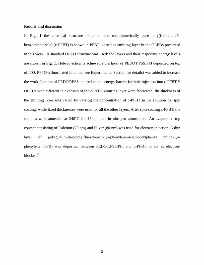
In Fig. 1 the chemical structure of chiral and enantiomerically pure poly(fluorene-alt-
benzothiadiazole) (c-PFBT) is shown. c-PFBT is used as emitting layer in the OLEDs presented
in this work. A standard OLED structure was used: the layers and their respective energy levels
are shown in Fig. 1. Hole injection is achieved via a layer of PEDOT:PSS:PFI deposited on top
of ITO. PFI (Perfluorinated Ionomer, see Experimental Section for details) was added to increase
the work function of PEDOT:PSS and reduce the energy barrier for hole injection into c-PFBT.22
OLEDs with different thicknesses of the c-PFBT emitting layer were fabricated; the thickness of
the emitting layer was varied by varying the concentration of c-PFBT in the solution for spin
coating, while fixed thicknesses were used for all the other layers. After spin-coating c-PFBT, the
samples were annealed at 240°C for 15 minutes in nitrogen atmosphere. An evaporated top
contact consisting of Calcium (20 nm) and Silver (80 nm) was used for electron injection. A thin
layer of poly2,7-9,9-di-n-octylfluorene-alt-1,4-phenylene-4-sec-butylphenyl imino-1,4-
phenylene (TFB) was deposited between PEDOT:PSS:PFI and c-PFBT to act as electron-
blocker.23
6
Figure 1. a) Chemical structure of c-PFBT. b) Layers comprising the OLED stack and their energy levels.
The dissymmetry factor gEL in the electro-luminescence of OLEDs comprising a c-PFBT
layer of 100, 200 and 400 nm thickness, operated in continuous voltage bias at 10, 15 and 25 V,
respectively, is shown in Fig. 2a. This corresponded to current densities of 340, 565 and 13
mA/cm2 and luminances of 900, 2950 and 80 cd/m2, respectively. The Current-Luminance-
Voltage characterization of the OLEDs is shown in Fig. S1. We define here the EL dissymmetry
factor gEL as:
gEL = 2·[ELL-ELR]/[ELL+ELR] (1)
where ELL and ELR are the EL intensities with left-handed and right-handed circular polarization,
respectively. The setup used to measure ELL and ELR is described in the experimental section.
We measured an excess of right-handed circularly polarization in the EL of all the OLEDs,
a)
b)

7
giving negative values of gEL according to the definition above. By increasing the thickness of
the c-PFBT emitting layer, gEL changes dramatically: with a c-PFBT layer thickness of 100 nm
we observe that gEL reaches a minimum value of -0.08 at 500 nm. Increasing the thickness of the
c-PFBT layer to 200 nm, gEL reaches -0.33 at 500 nm. We note that this is in line with the values
of gEL reported for most circularly polarized OLEDs to date (Supporting Table S1). When we
further increase the thickness of the c-PFBT layer to 400 nm, we obtain a minimum gEL of -0.6,
with the peak wavelength shifting to 520 nm. Not only the minimum value, but also the
dependence of gEL on wavelength varies with the thickness of the c-PFBT layer: with the 400 nm
thick OLED a band centred at 700-750 nm appears, as opposed to the thinner devices, where gEL
decreases monotonically with wavelength.
We have also measured CPEL under pulsed-voltage operation of the OLEDs: Fig. 2a
shows gEL measured on the 400 nm thick OLED when applying square voltage pulses (going
from 0 V to 35 V) with a duration of 1 µs, at a repetition rate of 1kHz; we observe that CPEL is
higher than in the continuous bias case, with gEL reaching -0.8 at 510 nm (i.e. corresponding to
40% excess of right-handed polarization). We found that gEL decreases when the duration of the
pulses is increased, reaching a less negative value of -0.65 at 525 nm under DC bias;
furthermore, the peak of gEL shifts to longer wavelengths for the longest pulses (250 µs) reaching
525 nm for the constant voltage case (Fig. S2, Supporting Information). The total, unpolarised,
EL of the same OLEDs is shown in Fig. 2b. We observe a red-shift of EL when going from 100
and 200 nm c-PFBT layers to 400 nm, with the peak of EL shifting from 535 nm to 545 nm. We
interpret the changes in EL spectrum as originating from different out-coupling of light when the
c-PFBT layer thickness is varied.

8
Figure 2. a) Dissymmetry factor of electro-luminescence gEL of OLEDs comprising a c-PFBT emitting layer of varying thickness (see legend). gEL was measured at constant voltage bias (“DC”, solid lines). gEL measured under 1µs, 35 V pulsed-voltage excitation (1kHz repetition rate) on the 400 nm thick OLED is also shown (circles). b) Corresponding total, unpolarized EL spectra under constant voltage bias.
All the CPEL results presented above were obtained on OLEDs in which the c-PFBT
layer had been thermally annealed at 240°C before evaporating the top contact. No CPEL was
detected on as-cast OLEDs. The dependence on annealing temperature and thickness of the
chiroptical properties of films of chirally substituted polyfluorenes is known: it was previously
shown that c-PFBT enters the cholesteric liquid crystalline phase when heated above 150°C.20
Furthermore, it was shown on chiral polyfluorenes that the circular polarization dissymmetry of
light transmitted through annealed films is strongly dependent on film thickness, owing to the
long range, non-local effect of the cholesteric dielectric on light polarization.21 Consistently with
these previous studies, we observe a 25-fold increase in apparent circular dichroism upon
500 550 600 650 700 750 800 850 9000.00.10.20.30.40.50.60.70.80.91.0
c-PFBT thickness 100 nm at 10 V - DC 200 nm at 15 V - DC 400 nm at 25 V - DC
Norm
alize
d EL
Wavelength (nm)
a)
b)
-0.8
-0.6
-0.4
-0.2
0.0
g EL
c-PFBT thickness 100 nm at 10 V - DC 200 nm at 15 V - DC 400 nm at 25 V - DC 400 nm at 35 V - 1µs pulse

9
thermal annealing of thin films of c-PFBT (Fig. 3a). The internal structural organization of the
film leads to unusual optical characteristics and we need therefore to take great care in the
definition of the experimental quantities under investigation. In Fig. 3a we show the difference
in extinction E = -log10(T) between transmission (T) of incident light having left and right
circular polarization, and using unpolarised (U) detection. The resulting quantity ELU – ER
U can
be regarded as an apparent circular dichroism where we note that in principle both absorption
and scattering can contribute to extinction. In the wavelength region above 500 nm, where the
polymer does not show allowed optical absorption, the circular differential extinction is mainly
due to circular selective scattering of light.
Fig. 3b and c show AFM microscopy images of as cast and annealed 400 nm thick films
deposited on fused silica substrates, respectively. As-cast films show spherical morphology (Fig.
3b), whereas upon annealing the morphology changes to an inter-connected network of fibres
(Fig. 3c). The fibres are typically ca. 200-300 nm wide. Polarized Optical Microscopy (POM)
with c-PFBT films between two crossed polarizers shows no birefringence for as cast films (Fig.
3d). In contrast, the annealed films do show birefringence, without any preferred orientation
(Fig. 3e). The image of the annealed film suggests small birefringent domains with dimensions
in the order of 1 micrometre. The strong dissymmetry in extinction and the presence of non-
oriented birefringence in POM indicate that upon thermal annealing multi-domain cholesteric
films are produced, containing cholesteric domains oriented at different angles between each
other. Note that we could not observe macroscopic circular selective reflection on the films; this
observation confirms the disordered nature of the films.24

10
Figure 3. a) Difference in extinction E for left and right circularly polarized incident light and unpolarized detection, for films of c-PFBT with thickness around 100 nm, before and after annealing at different temperatures (see legend). b,c) Tapping-mode AFM height images of as cast and annealed films respectively. d,e) Polarized optical microscopy (POM) images of as cast and annealed films respectively when viewed under cross-polarizer. All the films were deposited on fused silica substrates. The thermal annealing of films for AFM and POM was performed at 240 °C for 15 minutes.
The high degree of circular polarization in electro-luminescence (Fig. 2) and its relation
to the molecular organization induced by thermal annealing (Fig. 3) are intriguing and will now
be discussed in more detail. In Fig. 4a we show the chiroptical properties of an annealed film of
b) c)
d) e)
a)
As cast, 123 nm 150 °C, 98 nm 210 °C, 98 nm 240 °C, 104 nm
350 400 450 500 550 600 650 700-30
-20
-10
0
10
10
3 × (
E LU - E RU )
Wavelength (nm)

11
c-PFBT spin coated with the same thickness as used in the electro-luminescence measurements
(400 nm). We find very high values for the dissymmetry ratio in extinction defined as gEXT =
2·[ELU- ER
U]/[ ELU + ER
U]. Near the onset of the absorption we find gEXT = -0.8. The
dissymmetry ratio for photo-luminescence gPL = 2·[IL-IR]/[IL+IR], with IL and IR the intensity of
left and right circularly polarized luminescence for the same 400 nm thick film, also reaches high
values near the onset of the luminescence: gPL = -0.6. The photo-luminescence has been
measured using unpolarised excitation light with 356 nm wavelength and with direction normal
to the film and in line with the direction of luminescence collection. The similarity between gEXT
and gPL at the onsets of the absorption and luminescence bands is consistent with the expected
time reversal symmetry for photon absorption and emission near the origin of the bands. The
high values for gEL, gEXT and gPL are all consistent with a non-local origin of the circular
polarization related to a cholesteric organization within the film.
The next issue we address is how the peculiar multi-domain cholesteric organization in
the films under study can lead to such high degrees of polarization in photo- and electro-
luminescence. The hypothesis we investigate is that the light produced by electro-luminescence
acquires its polarization characteristics while it travels through the film in the outward direction,
after the corresponding photon has been generated. In order to test this hypothesis we
investigated the transmission of light in the wavelength range corresponding to the emission. In a
first naïve approach, we assume that initially the emission is unpolarised and that the relative
circular differential transmission of the left and right circular components of the emission lead to
net circular polarization. In Fig. 4b we illustrate the dissymmetry ratio gTRANS = 2·[TLU -
TRU]/[TL
U + TRU] for transmission of left and right circularly polarized incident light and
unpolarised detection, for thermally annealed films of c-PFBT with different thicknesses. For the

12
thickest film (400 nm), a broad band in the gTRANS spectrum appears for wavelengths near 1100
nm (see inset in Fig. 4b). Because the polymer has no absorption band in this region and does
not show any detectable circular selective reflection of light, we assign the negative gTRANS to
preferential scattering of left circularly polarized light. The sign and wavelength are consistent
with a left-handed cholesteric organization with pitch length around 600 nm and refractive index
near 1.7. In the wavelength range 490-700 nm relevant for the emission, the degree of
polarization is on the order of 10-2 (preferred right-handed transmission). These results show that
selective scattering can at least partially contribute to the circular polarization of EL observed in
the OLEDs.
A second non-local effect that can impact the CPEL in our OLEDs is birefringence.
Using a rubbed polyimide alignment layer as substrate for thin thermally annealed films of
c-PFBT, we found that the absorption of light involving the allowed transition to the lowest
singlet excited state (S1) is highly linearly polarized parallel to the rubbing direction of the
alignment layer. This is consistent with the orientation of the transition dipole moment of the
S1←S0 transition parallel to the direction of the backbone of the polymer. The luminescence
involving the reverse S1 → S0 transition is therefore expected to be initially polarized in a
direction parallel to the polymer chain. However the strong birefringence of the annealed
polymer films may change the polarization of this initially linearly polarized light. Because of
the cholesteric arrangement of the polymer chains one expects some birefringence in a direction
making an angle of 45o with the direction of the polymer chains involved in generation the
luminescence. This particular birefringence will convert linearly polarized light into circularly
polarized light and contribute to the overall circular polarization of the luminescence. In order to
test this scenario experimentally we have performed generalized ellipsometry on polymer films
13
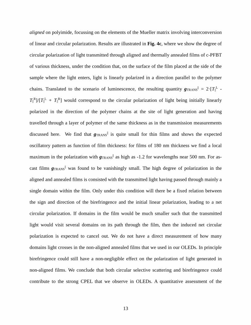
aligned on polyimide, focussing on the elements of the Mueller matrix involving interconversion
of linear and circular polarization. Results are illustrated in Fig. 4c, where we show the degree of
circular polarization of light transmitted through aligned and thermally annealed films of c-PFBT
of various thickness, under the condition that, on the surface of the film placed at the side of the
sample where the light enters, light is linearly polarized in a direction parallel to the polymer
chains. Translated to the scenario of luminescence, the resulting quantity gTRANS|| = 2·[T||
L -
T||R]/[T||
L + T||R] would correspond to the circular polarization of light being initially linearly
polarized in the direction of the polymer chains at the site of light generation and having
travelled through a layer of polymer of the same thickness as in the transmission measurements
discussed here. We find that gTRANS|| is quite small for thin films and shows the expected
oscillatory pattern as function of film thickness: for films of 180 nm thickness we find a local
maximum in the polarization with gTRANS|| as high as -1.2 for wavelengths near 500 nm. For as-
cast films gTRANS|| was found to be vanishingly small. The high degree of polarization in the
aligned and annealed films is consisted with the transmitted light having passed through mainly a
single domain within the film. Only under this condition will there be a fixed relation between
the sign and direction of the birefringence and the initial linear polarization, leading to a net
circular polarization. If domains in the film would be much smaller such that the transmitted
light would visit several domains on its path through the film, then the induced net circular
polarization is expected to cancel out. We do not have a direct measurement of how many
domains light crosses in the non-aligned annealed films that we used in our OLEDs. In principle
birefringence could still have a non-negligible effect on the polarization of light generated in
non-aligned films. We conclude that both circular selective scattering and birefringence could
contribute to the strong CPEL that we observe in OLEDs. A quantitative assessment of the

14
contribution of the two mechanisms is beyond the scope of the present work.
Figure 4. a) Dissymmetry ratio gEXT = 2(EL
U-ERU)/( EL
U+ERU) for extinction of left and right
circularly polarized incident light and unpolarized detection on a 400 nm thick, thermally annealed film of c-PFBT on fused silica. In red, the dissymmetry ratio for photo-luminescence gPL= 2[IL-IR]/[IL+IR] for the same film is shown. Photo-luminescence intensity I was recorded upon excitation with unpolarized light of 356 nm entering the film under normal incidence and propagating in the same direction as used for the emission detection. b) Dissymmetry ratio gTRANS = 2(TL
U-TRU)/( TL
U+TRU) for thermally annealed, non-aligned films of c-PFBT with
different thicknesses. The inset shows the circular selective scattering band for the 400 nm thick film in the near infrared spectral range. c) Dissymmetry ratio gTRANS
|| = 2(T||
L-T||R)/( T||
L+T||R) for
aligned films of c-PFBT of different thicknesses, with T||L (T||
R) denoting the transmission of light that is linearly polarized in the direction parallel to the polymer chains upon entering the film and that leaves the film with left- (right-) handed circular polarization.
To further investigate the impact on CPEL of the disorder present in our multi-domain
emitting layers, we have used a model that was developed by Dmitrienko and Belyakov for
500 550 600 650 700-0.03-0.02-0.010.000.010.020.03
1000 1500-0.02
-0.01
d = 80 nm
180 nm
400 nm
g TRA
NS
non-aligned films
500 600 700 800 900
-1.0
-0.5
0.0
300 nm
180 nm
24 nm
g TRA
NS ||
Wavelength (nm)
aligned films
300 400 500 600-0.8
-0.6
-0.4
-0.2
0.0
0.2
gEX
T & g
PL
λexc = 356 nmd = 400 nm
a)
b)
c)

15
transmission of light through an imperfect cholesteric liquid crystal.25 Here we used their model
to study the effect of the distribution in size and orientation of the cholesteric domains on the
circular polarization of EL coming out of the OLED in the normal direction with respect to the
substrate. The model considers selective reflection events at individual domains; light waves
reflected from or transmitted through different domains are considered to superimpose
incoherently, that is with random phases. For the film as a whole, the multiple incoherent
reflections amount to scattering of light. Reflection at an individual domain of light with the
same handedness as that of the cholesteric is described by:
𝑟𝑟(𝛼𝛼) = 𝐵𝐵 1−cos (𝛼𝛼𝛼𝛼ℎ)𝛼𝛼2𝛼𝛼ℎ
(2)
where
𝐵𝐵 = 𝛿𝛿2
8𝑠𝑠𝑠𝑠𝑠𝑠2𝜃𝜃 (3)
and
𝛼𝛼(𝑘𝑘) = (2𝜋𝜋𝑝𝑝 )−2𝛼𝛼𝑠𝑠𝑠𝑠𝑠𝑠𝜃𝜃
𝛼𝛼 (4)
In Equation (3), δ is defined as δ = (ε1-ε2)/(ε1+ε2), where ε1 and ε2 are the components of the
complex dielectric tensor in the plane normal to the axis of the cholesteric helix. In Equation (4)
p is the pitch of the cholesteric and k the wave-vector of light in the dielectric, defined by 𝑘𝑘 =
2𝜋𝜋𝜆𝜆 𝜀𝜀1/2, where λ is the wavelength of light in the vacuum and 𝜀𝜀 is the average dielectric
function. In Equation (2) h is the thickness of the cholesteric domain, while in Equation (3) θ is
the angle at which light impinges on the domain. The polarization of light emerging out of the
OLED depends also on the total thickness T of the film from the site of emission to the interface

16
with the transparent electrode. T, h and θ are schematically represented in Fig. 5a. The
components ε1 and ε2 of the dielectric tensor were measured by ellipsometry on a thin film (23
nm) on quartz. The dependence of δ2 on wavelength obtained from the measured components of
the dielectric tensor is shown in Fig. S3. As mentioned above, the cholesteric pitch in our films
was measured to be 600 nm.
B is almost constant at long wavelengths away from resonance, while it increases sharply
approaching the onset of light absorption, due to the increase in δ2 (Fig. S3). The range of
wavelengths close to the onset of absorption is particularly relevant in our case, since it is where
the peak of electro-luminescence occurs. The term 1−cos (𝛼𝛼𝛼𝛼ℎ)𝛼𝛼2𝛼𝛼ℎ
in Equation (2) takes into account
the Bragg-type circular selective reflection of light on a single cholesteric domain.
Following the formalism of ref. 25 we calculate the dissymmetry factor gEL of the EL
emitted along the direction normal to the substrate (Fig. 5a) using Equation (1) and the following
expression for ELL and ELR:
𝐸𝐸𝐸𝐸𝐿𝐿 = 𝑚𝑚(𝜇𝜇+𝜇𝜇𝑑𝑑) sinh(𝑚𝑚 𝑇𝑇)+𝑚𝑚 𝑐𝑐𝑐𝑐𝑠𝑠ℎ(𝑚𝑚 𝑇𝑇)
(5)
𝐸𝐸𝐸𝐸𝑅𝑅 = 𝑒𝑒−𝜇𝜇𝑇𝑇 (6)
where m = (μ2+2μμd )1/2, μ is the linear absorption coefficient, and 𝜇𝜇𝑑𝑑 = 4𝑘𝑘𝑟𝑟, with r defined in
Equation (2) and k the wave-vector of light in the dielectric.
We consider the limiting case in which light-emission occurs with linear polarization and
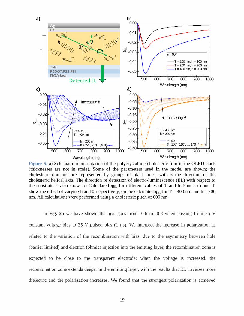
close to the cathode, with light traversing the whole emitting layer before being emitted. Fig. 5b
shows the calculated absolute dissymmetry factor gEL as function of wavelength and film
thickness, using θ = 90°. The simulated dependence of gEL on film thickness is in agreement with
17
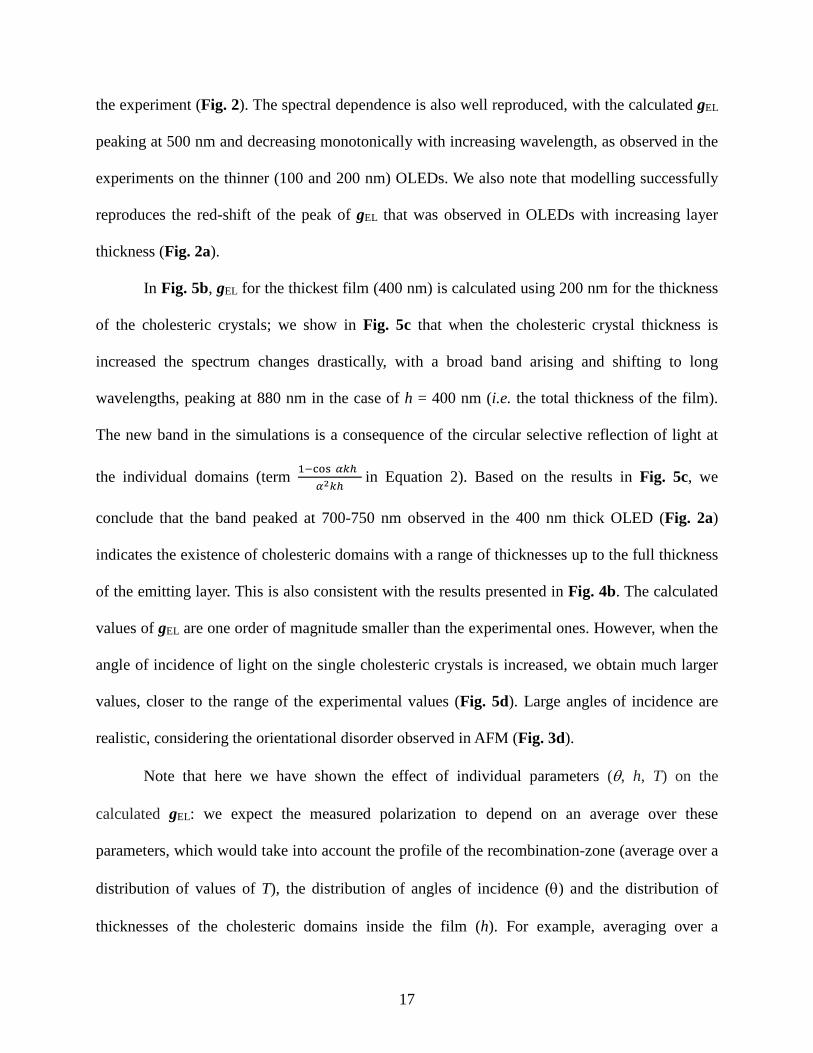
the experiment (Fig. 2). The spectral dependence is also well reproduced, with the calculated gEL
peaking at 500 nm and decreasing monotonically with increasing wavelength, as observed in the
experiments on the thinner (100 and 200 nm) OLEDs. We also note that modelling successfully
reproduces the red-shift of the peak of gEL that was observed in OLEDs with increasing layer
thickness (Fig. 2a).
In Fig. 5b, gEL for the thickest film (400 nm) is calculated using 200 nm for the thickness
of the cholesteric crystals; we show in Fig. 5c that when the cholesteric crystal thickness is
increased the spectrum changes drastically, with a broad band arising and shifting to long
wavelengths, peaking at 880 nm in the case of h = 400 nm (i.e. the total thickness of the film).
The new band in the simulations is a consequence of the circular selective reflection of light at
the individual domains (term 1−cos (𝛼𝛼𝛼𝛼ℎ)𝛼𝛼2𝛼𝛼ℎ
in Equation 2). Based on the results in Fig. 5c, we
conclude that the band peaked at 700-750 nm observed in the 400 nm thick OLED (Fig. 2a)
indicates the existence of cholesteric domains with a range of thicknesses up to the full thickness
of the emitting layer. This is also consistent with the results presented in Fig. 4b. The calculated
values of gEL are one order of magnitude smaller than the experimental ones. However, when the
angle of incidence of light on the single cholesteric crystals is increased, we obtain much larger
values, closer to the range of the experimental values (Fig. 5d). Large angles of incidence are
realistic, considering the orientational disorder observed in AFM (Fig. 3d).
Note that here we have shown the effect of individual parameters (θ, h, T) on the
calculated gEL: we expect the measured polarization to depend on an average over these
parameters, which would take into account the profile of the recombination-zone (average over a
distribution of values of T), the distribution of angles of incidence (θ) and the distribution of
thicknesses of the cholesteric domains inside the film (h). For example, averaging over a

18
distribution of cholesteric domain thicknesses h would result in a broad spectrum of gEL, as can
be appreciated from Fig. 5c, and would explain the broad gEL spectrum observed experimentally
in the 400 nm thick OLED (Fig. 2a). We do not have a direct measurement of the exact
distribution of domain size and orientation in the films, which would be necessary for a more
quantitative treatment. Furthermore, here we have not included wave-guiding of EL in the
emitting layer and reflection at the back metal electrode, which could also impact the spectral
shape and intensity of CPEL.
19
Figure 5. a) Schematic representation of the polycrystalline cholesteric film in the OLED stack (thicknesses are not in scale). Some of the parameters used in the model are shown; the cholesteric domains are represented by groups of black lines, with z the direction of the cholesteric helical axis. The direction of detection of electro-luminescence (EL) with respect to the substrate is also show. b) Calculated gEL for different values of T and h. Panels c) and d) show the effect of varying h and θ respectively, on the calculated gEL for T = 400 nm and h = 200 nm. All calculations were performed using a cholesteric pitch of 600 nm.
In Fig. 2a we have shown that gEL goes from -0.6 to -0.8 when passing from 25 V
constant voltage bias to 35 V pulsed bias (1 µs). We interpret the increase in polarization as
related to the variation of the recombination with bias: due to the asymmetry between hole
(barrier limited) and electron (ohmic) injection into the emitting layer, the recombination zone is
expected to be close to the transparent electrode; when the voltage is increased, the
recombination zone extends deeper in the emitting layer, with the results that EL traverses more
dielectric and the polarization increases. We found that the strongest polarization is achieved
a) b)
c) d)
500 600 700 800 900 1000
-0.05
-0.04
-0.03
-0.02
-0.01
0.00
g EL
Wavelength (nm)
θ = 90°
T = 100 nm, h = 100 nm T = 200 nm, h = 200 nm T = 400 nm, h = 200 nm
500 600 700 800 900 1000
-0.05
-0.04
-0.03
-0.02
-0.01
0.00
Wavelength (nm)
g EL
increasing h
θ = 90°T = 400 nm
h = 200 nm h = 225, 250,...,400( )
500 600 700 800 900 1000-0.40-0.35-0.30-0.25-0.20-0.15-0.10-0.050.00
g EL
Wavelength (nm)
T = 400 nmh = 200 nm
θ = 90° θ = 100°, 110°, ..., 140° ( )
increasing θ

20
with short bias pulses, while gEL reduces when the length of the pulses at 35 V is increased (Fig.
S2): this effect is possibly due to local heating affecting the dielectric function of the emitting
layer. Heating is expected to be non-negligible at the high voltages applied on thick layers and is
likely to be stronger when using long pulses or constant voltage. Our results suggest that the
standard OLED structure used in this work limits the highest gEL that is possible to obtain for a
given thickness of the emitting layer, due to the unfavourable position of the recombination zone
close to the transparent anode. Tuning the OLED structure in order to have the recombination
zone farther from the transparent contact will allow high gEL at lower driving voltages. The
position of the recombination zone could be varied for example by choice of transport layers. In
general, the rather large thickness of the cholesteric emitting layer required by our non-local
approach to strong CPEL presents a challenge to achieving high performance devices: to reach
substantial charge injection and light emission, high driving voltages are required in the thick
structures. This in turn hinders power efficiency, as can be seen in Fig. S1. This limitation could
be overcome by improving charge injection; Kabra et al. have previously demonstrated that
ohmic hole injection in inverted-structure polymer LEDs allows to use thick emitting layers
while maintaining high power efficiency.26 We believe that if efficient charge injection is
obtained in concert with optimal position of the recombination zone far from the transparent
anode, strong CPEL and high power efficiency can be achieved simultaneously.
It is also worth recalling here the results by Zinna et al. in OLEDs based on chiral
lanthanide complexes, where EL is strongly polarized at the site of emission (i.e. locally)9: in
their study it was found that to maximize gEL the recombination zone has to be positioned as
close as possible to the transparent anode, to minimize the contribution of light which has
switched to opposite polarization handedness after reflection at the metallic back electrode. It is

21
therefore interesting to note how different mechanisms of CPEL generation translate into
different requirements for the position of the recombination zone.
Finally, we show on a 100 nm thick c-PFBT OLEDs that circular polarization can be
switched ON and OFF when short, high-voltage pulses are applied. The short pulses allow us to
use a large range of applied voltages without damaging the OLEDs. Fig. 6 shows gEL in two
different cases: 6V, 10 µs-long square pulses and 20V, 5 µs-long square pulses. The repetition
rate was 1 kHz in both cases. We observe that no polarization is present when 6V pulses are
applied, while gEL = -0.15 at 500 nm is achieved with 20 V pulses. Similarly to the case of the
400 nm thick layer described above, we interpret this observation in terms of the recombination
zone depth in the emitting layer: at 6V and with a 10 µs pulses the recombination zone is
expected to be narrow and close to the transparent electrode; under these conditions the actual
dielectric thickness that EL travels across is close to zero and virtually no polarization can occur.
At 20 V, instead, there is enough electric field across the c-PFBT layer to extend the
recombination zone deeper, towards the back electrode. Hence a relatively large value of gEL is
achieved, ca. 2-fold higher (at 500 nm) than the one recorded when using a 10 V constant bias
(Fig. 2a).

22
500 550 600 650 700 750 800 850 900-0.20
-0.15
-0.10
-0.05
0.00
0.05
100 nm c-PFBT 6 V, 10 µs 20 V, 5 µs
Wavelength (nm)
g EL
Figure 6. Dissymmetry factor of electro-luminescence gEL of an OLEDs comprising a 100 nm c-PFBT, measured under pulsed-voltage excitation at 6 V, 10 µs (red symbols) and 20 V, 5 µs (black symbols). A repetition rate of 1kHz was used in both cases.
Conclusions
In conclusion, in this work we have shown very strong circular polarization of electro-
luminescence from single-layer, solution processed polymer OLEDs based on a chiral
enantiomerically pure polyfluorene copolymer as emitting material; when using a thermally
annealed and thick (400 nm) polymer emitting layer we recorded up to 40% excess of right-
handed circular polarization under pulsed voltage bias operation (gEL = -0.8) and 30% (gEL =
-0.6) under constant voltage bias. These are between the highest values of CPEL reported for
OLEDs and the highest achieved without the use of chiral dopants or alignment layers. We also
showed that CPEL can be controlled electrically by varying the OLED operation mode, adding a
further functionality to these devices.
We find that thermal annealing produces cholesteric films with domains having

23
orientational and size disorder throughout the sample. The disordered, multi-domain cholesteric
films show no appreciable circular selective reflection. Yet domains are large enough to give rise
to circular selective scattering and linear birefringence that is correlated in direction to the initial
linear polarization of the luminescence photon. Experimental determination of the Mueller
matrix of the films show efficient conversion of linearly polarized light into circularly polarized
radiation. We conclude that the high levels of CPEL measured in our devices arise mainly after
the photon has been generated during the passage of the photon through the film in the outward
direction. The genesis of circular polarization involves selective scattering and birefringence.
We believe that the approach to CPEL based on non-local effects (circular selective
scattering and birefringence) in multi-domain cholesterics is very promising because of the ease
of fabrication, only requiring thermal annealing. Another crucial advantage is that at wavelengths
close to resonance, where most electro-luminescence from the polymer occurs, high polarization
can be achieved due to the strong dielectric anisotropy: this might not always be possible in a
mono-domain cholesteric film, depending on the pitch length and the resulting Bragg reflection
conditions. Furthermore, we show that CPEL in our devices is broad-band, another aspect that is
generally difficult to obtain if relying only on Bragg reflection in a perfect, mono-domain
cholesteric. Finally, we note that because the cholesteric domains are scattering centres, a
beneficial impact on the out-coupling of EL in the direction normal to the OLED substrate might
be expected.
Our work demonstrates a facile and generally applicable fabrication route to obtain
OLEDs with high levels of circular polarization; we foresee that 100 % polarized broad-band
CPEL can be achieved in OLEDs with thick (a few hundreds of nanometres) multi-domain
cholesteric emitting layers: this will involve tuning charge mobility and injection, in order for the

24
recombination zone to be located far from the transparent contact, already at low driving voltage.
More generally, we demonstrate that chirally-substituted conjugated polymers can combine
semiconducting and photonic functionalities: this makes them an interesting class of materials
for advanced manipulation of light in optoelectronic devices.
Methods
Synthesis of c-PFBT: c-PFBT was synthesized19 and further purified to remove palladium
catalyst according to reported procedures.27, 28
2,7-bis(pinacoyl)-9,9-bis((S)-3,7-dimethyloctyl)fluorene boronic ester (616 mg, 0.88 mmol, 1.0
eq.), 4,7-dibromobenzothiadiazole (259 mg, 0.88 mmol, 1.0 eq.) and oven dried (140 ˚C) sodium
carbonate (981 mg, 9.25 mmol, 10.5 eq.) were taken in a 3-necked round bottom flask (100 mL)
fitted with a reflux condenser and an argon inlet. The flask was evacuated and back-filled with
argon three times. Tetrakis(triphenylphosphine)palladium (0) catalyst (51 mg, 0,044 mmol, 0.05
eq.) weighed under an argon atmosphere was added to the RBF under positive argon pressure.
The flask was again evacuated and back-filled with argon three times. A 2:1 (v/v) mixture of
dioxane:water (25 mL) was degassed by three cycles of freeze-pump-thaw and added to the RBF
and the reaction mixture was heated to 95 ˚C (oil bath) for 3 days. Then the end capper, 2-
pinacoyl-9,9-bis((S)-3,7-dimethyloctyl)fluorene boronic ester (101 mg, 0.17 mmol, 0.2 eq.)
dissolved in dioxane (degassed by three cycles of freeze-pump-thaw, 6 mL) was added to the
RBF and the reaction was continued overnight. The reaction mixture was allowed to cool down
to room temperature and extracted with chloroform and1M HCl. The organic layer was washed
with sat. NaHCO3 and finally with brine. The organic layer was dried over sodium sulfate and
concentrated to about 150 mL.
25
Purification: To the organic layer (CHCl3, 150 mL), 28-30% aq. ammonia solution (150 mL) was
added and refluxed (oil bath at 85 ˚C) for 3 hours and then stirred overnight at room temperature.
Next day, the solution was transferred to a separating funnel and extracted with excess water. To
the collected organic layer, ethylenediamine tetra-acetic acid disodium salt dihydrate (1.2 g) was
addednd further stirred at room temperature overnight. After 15 hours, the organic layer was
extracted with water, dried (over sodium sulfate) and evaporated to about 10-15 mL. To this
concentrated solution, a palladium scavenger agent, diethyldithiocarbamic acid
diethylammonium salt (25 mg) was added and stirred under dark and argon atmosphere at room
temperature for 8 hours. Immediately after addition of the scavenger, the dark coloured solution
turned orange. After 8 hours, the solution was poured into cold methanol (250 mL) and the
yellow precipitate was collected by suction filtration and dried under vacuum at 60 ˚C overnight.
The precipitate was then subjected to soxhlet extraction with first acetone and finally with
chloroform (oil bath at 85 ˚C) for 24 hours each. The chloroform was concentrated to about 10
mL and poured into cold methanol (300 mL). The precipitate was collected by suction filtration
and dried under vacuum at 60 ˚C for 24 hours to obtain yellow solid (440 mg, 82% yield).
1H-NMR (400 MHz, CDCl3): δ = 8.11-8.09 (m, 2H), 8.02-7.86 (m, 6 H), 2.16 (m, 4H), 1.44-1.36
(m, 2H), 1.30-0.85 (m, 19H), 0.85-0.6 ppm (m, 24H).
13C-NMR (100 MHz, CDCl3): δ = 154.55, 151.82, 141.14, 136.66, 133.82, 128.48, 128.08,
124.12, 120.17, 55.42, 39.42, 37.68, 36.86, 33.18, 30.94, 28.06, 24.88, 22.79, 22.69, 19.80 ppm.
Both 1H- and 13-C NMR spectra are in agreement with what reported in literature.20
GPC (PS standard, THF); Apparent Mn: 15.36 kg mol-1, Mw: 31.77 kg mol-1, PDI (Mw/Mn) =
2.06
OLED fabrication and characterization: OLEDs were fabricated by spin coating in air (5000
26
RPM, 2000 RPM/s acceleration) a mixture of PEDOT:PSS
(poly(ethylenedioxythiophene):poly(styrene sulfonate), Clevios P VP Al4083) and PFI (Nafion®
perfluorinated resin solution, 5 wt. % in lower aliphatic alcohols and water, containing 15-20%
water, Sigma-Aldrich) onto pre-cleaned, patterned indium tin oxide (ITO) substrates (15 Ω per
square, Colorado Concept Coatings). PEDOT:PSS:PFI was prepared in the weight ratio 1:6:11.2.
The PEDOT:PSS:PFI layer was annealed at 200°C for 20 minutes under N2 atmosphere.
Subsequently, a layer of TFB (Poly[(9,9-dioctylfluorenyl-2,7-diyl)-co-(4,4′-(N-(4-sec-
butylphenyl)diphenylamine)], Mp = 119 Kg/mol, Mn = 60 Kg/mol) was spin coated (2000 RPM,
2000 RPM/s acceleration) using a 8 mg/ml solution in toluene. The TFB layer was thermally
annealed at 180°C for 20 minutes under N2 atmosphere before depositing the c-PFBT layer. To c-
PFBT layer was spin coated at 2000 RPM, 2000RPM/s acceleration, with concentration varied
between 15 and 40 mg/mL in toluene to achieve different thicknesses. At this point the stack was
further annealed at 240 °C, for 15 minutes and rapidly cooled afterwards. Finally, 10 nm of
Calcium and 80 nm of Silver were thermally evaporated at a pressure of 10-6 mbar. The devices
were encapsulated to limit degradation during the measurements. The OLEDs had an active area
of 4.5 mm2. Current-luminance-voltage curves were recorded in a setup consisting of a Keithley
2400 source meter and a calibrated silicon photodiode. The thickness of the c-PFBT layer was
measured with a Bruker Dektak profilometer.
Measurement of Circularly Polarized Electro-Luminescence: electro-luminescence (EL) spectra
were recorded by using an Andor Shamrock spectrometer (model SR-303i-B), equipped with a
silicon CCD (model iDUS DU420A). The EL spectra were corrected for the response of the
spectrometer and detector. Circular polarization was measured by placing a broad-band λ/4
waveplate (Thorlabs, AQWP05M-600) between the OLED and a linear polarizer. Measurements

27
were conducted using the direction of EL normal to the OLED substrate, the λ/4 waveplate and
the linear polarizer. ELL and ELR were measured by rotating the fast axis of the λ/4 waveplate at
an angle of -45° (+45°) with respect to the polarization axis of the linear polarizer, respectively.
The linear polarizer was maintained in a fixed position to avoid artefacts arising from the
sensitivity of the monochromator to linear polarization. A 2400 Keithley source meter was used
to drive the OLEDs in constant voltage bias. A function generator (Hewlett Packard, model
8116A) coupled with a home-built high-voltage source was used for the pulsed-voltage
experiments. The voltage pulses were obtained from a square wave at a repetition rate of 1 kHz,
with the duration of the high-voltage state varied between 1µs and 250 µs and the 0V state
maintained for the rest of the cycle. All the experiments were conducted at room temperature.
Microscopy: Atomic Force Microscopy (AFM): AFM was carried out using Asylum Research
MFP-3D mounted on an anti-vibration stage. Silicone probes manufactured by NanoSensors™
(model PPP-NCSTR-50) with a tip height of 10-15 µm and radius of < 10 nm was used for AC
tapping-mode measurement. A scan rate of 0.8 Hz and pixel size of 512×512 resolution was
used. The images were subjected to first order flattening using Gwyddion (v. 2.48) software.
Polarized Optical Microscopy (POM): POM images were acquired on a Leica DM 2700 M
optical microscope equipped with cross polarizers.
Circular dichroism: Circular dichroism (CD) measurements on film with thickness d < 140 nm
were done on JASCO J-815 spectrometer using a scan speed of 100 nm min-1, data pitch of 0.1
nm, response time of 1 second and band width of 1.71. Linear dichroism (LD) was measured on
all the samples and no significant LD was observed for the samples studied. CD results on thick,
d > 140 nm, films were obtained from generalized ellipsometry with a Woollam WVASE unit.
The (1,4) element of the Mueller matrix in transmission geometry equals -1/2 times the

28
dissymmetry ratio for transmission, gTRANS. Combining the Mueller matrix determination with
independent measurement of the transmission, the extinctions ELU and ER
U can be calculated in a
straight forward manner. The (2,4) element of the Mueller matrix measured on an aligned film
with alignment layer on the detector side and rubbing direction equals 1/2 times gTRANS||.
Sample preparation for optical and microscopy studies: thin films were spin-coated from
solution of c-PFBT with varying concentrations (from 5 mg/mL to 50 mg/mL) to obtain a range
of thicknesses. All films were spin-coated from toluene, with the exception of thin films for
circular dichroism (Fig. 3a) and aligned films (Fig. 4c), which were spin-coated from a solution
of c-PFBT in 9:1 (v/v) chloroform:chlorobenzene. The solutions were spin-coated (2000 rpm, 60
seconds) on cleaned glass or fused silica substrates. All annealed samples were annealed for 15
minutes under nitrogen atmosphere (glove box). The film thicknesses of all films were measured
using a Dektak 150 surface profiler.
Polyimide alignment layer: 2.5 cm × 2.5 cm glass slides were cleaned by sonication for 10
minutes each with acetone and isopropyl alcohol. The glass slides were then etched in a UV-
ozone photoreactor (PR-100) for 30 minutes. Polyimide (AL 1051) was spin-coated on etched
glass-slides (5000 rpm, 40 seconds, 500 rpm acceleration) and then annealed at 180 ˚C for 90
minutes. The polyimide facing side was rubbed on a velvet cloth to induce planar alignment.
Circular polarization of photo-luminescence: Measurements were done using a home-built setup
employing a photo-elastic modulator and a 16-channel photomultiplier array involving a photon
counting detection scheme. 365 nm excitation light was selected from a Hg lamp using
appropriate interference and bandpass filters. The excitation light was depolarized by passing it
through a bundle of optical fibres. The direction of the excitation was normal to the surface of
the film and in line with the direction of emission collection.

29
Ellipsometry: Generalized ellipsometry measurements were carried out with the Woollam
WVASE ellipsometer using the general Mueller matrix measurement protocol.
Corresponding Author
* Daniele Di Nuzzo ([email protected])
Acknowledgements
D.D.N. and R.H.F. acknowledge financial support from the Engineering and Physical Sciences
Research Council of the UK (EPSRC). C.K. and E.W.M. acknowledge financial support from
the Dutch Ministry of Education, Culture and Science (Gravity program 024.001.035). C.K.
thanks financial support from Marie Skłodowska-Curie (704830) postdoctoral fellowship.
Supporting Information Available: Current-Luminance-Voltage characteristics, gEL as
function of operation mode, experimental values of δ2. This material is available free of charge
via the Internet at http://pubs.acs.org.
References
(1) Hövel, S.; Gerhardt, N. C.; Hofmann, M. R.; Lo, F.-Y.; Reuter, D.; Wieck, A. D.;
Schuster, E.; Keune, W.; Wende, H.; Petracic, O.; et al. Electrical Detection of Photoinduced
Spins Both at Room Temperature and in Remanence. Appl. Phys. Lett. 2008, 92, 242102.
30
(2) Farshchi, R.; Ramsteiner, M.; Herfort, J.; Tahraoui, A.; Grahn, H. T. Optical
Communication of Spin Information between Light Emitting Diodes. Appl. Phys. Lett. 2011, 98,
162508.
(3) Wang, C. S.; Fei, H. S.; Qiu, Y.; Yang, Y. Q.; Wei, Z. Q. Photoinduced Birefringence and
Reversible Optical Storage in Liquid-Crystalline Azobenzene Side-Chain Polymers. Appl. Phys.
Lett. 1999, 74, 19–21.
(4) Liu, C.; Yang, D.; Jin, Q.; Zhang, L.; Liu, M. A Chiroptical Logic Circuit Based on Self-
Assembled Soft Materials Containing Amphiphilic Spiropyran. Adv. Mater. 2016, 28, 1644–
1649.
(5) Novikova, T.; Pierangelo, A.; Manhas, S.; Benali, A.; Validire, P.; Gayet, B.; De Martino,
A. The Origins of Polarimetric Image Contrast between Healthy and Cancerous Human Colon
Tissue. Appl. Phys. Lett. 2013, 102, 241103.
(6) Kunnen, B.; Macdonald, C.; Doronin, A.; Jacques, S.; Eccles, M.; Meglinski, I.
Application of Circularly Polarized Light for Non-Invasive Diagnosis of Cancerous Tissues and
Turbid Tissue-like Scattering Media. J. Biophotonics 2015, 8, 317–323.
(7) McNichols, R. J.; Cote, G. L. Optical Glucose Sensing in Biological Fluids: An
Overview. J. Biomed. Opt. 2000, 5, 5–16.
(8) Lee, D.-M.; Song, J.-W.; Lee, Y.-J.; Yu, C.-J.; Kim, J.-H. Control of Circularly Polarized
Electroluminescence in Induced Twist Structure of Conjugate Polymer. Adv. Mater. 2017, 29,
1700907.
(9) Zinna, F.; Pasini, M.; Galeotti, F.; Botta, C.; Di Bari, L.; Giovanella, U. Design of
Lanthanide-Based OLEDs with Remarkable Circularly Polarized Electroluminescence. Adv.
Funct. Mater. 2017, 27, 1603719.

31
(10) Brandt, J. R.; Wang, X.; Yang, Y.; Campbell, A. J.; Fuchter, M. J. Circularly Polarized
Phosphorescent Electroluminescence with a High Dissymmetry Factor from PHOLEDs Based on
a Platinahelicene. J. Am. Chem. Soc. 2016, 138, 9743–9746.
(11) Li, T.-Y.; Jing, Y.-M.; Liu, X.; Zhao, Y.; Shi, L.; Tang, Z.; Zheng, Y.-X.; Zuo, J.-L.
Circularly Polarised Phosphorescent Photoluminescence and Electroluminescence of Iridium
Complexes. Sci. Rep. 2015, 5, 14912.
(12) Han, J.; Guo, S.; Wang, J.; Wei, L.; Zhuang, Y.; Liu, S.; Zhao, Q.; Zhang, X.; Huang, W.
Circularly Polarized Phosphorescent Electroluminescence from Chiral Cationic Iridium(III)
Isocyanide Complexes. Adv. Opt. Mater. 2017, 5, 1700359.
(13) Peeters, E.; Christiaans, M. P. T.; Janssen, R. A. J.; Schoo, H. F. M.; Dekkers, H.; Meijer,
E. W. Circularly Polarized Electroluminescence from a Polymer Light-Emitting Diode. J. Am.
Chem. Soc. 1997, 119, 9909–9910.
(14) Oda, M.; Nothofer, H. G.; Lieser, G.; Scherf, U.; Meskers, S. C. J.; Neher, D. Circularly
Polarized Electroluminescence from Liquid-Crystalline Chiral Polyfluorenes. Adv. Mater. 2000,
12, 362–365.
(15) Geng, Y. H.; Trajkovska, A.; Culligan, S. W.; Ou, J. J.; Chen, H. M. P.; Katsis, D.; Chen,
S. H. Origin of Strong Chiroptical Activities in Films of Nonafluorenes with a Varying Extent of
Pendant Chirality. J. Am. Chem. Soc. 2003, 125, 14032–14038.
(16) Yang, Y.; da Costa, R. C.; Smilgies, D.-M.; Campbell, A. J.; Fuchter, M. J. Induction of
Circularly Polarized Electroluminescence from an Achiral Light-Emitting Polymer via a Chiral
Small-Molecule Dopant. Adv. Mater. 2013, 25, 2624–2628.

32
(17) Blok, P.; Dekkers, H. Discrimination Between 3-Pi-Pi-Star and 3n-Pi-Star States in
Organic Molecules by Circular-Polarization of Phosphorescence. Chem. Phys. Lett. 1989, 161,
188–194.
(18) Lunkley, J. L.; Shirotani, D.; Yamanari, K.; Kaizaki, S.; Muller, G. Extraordinary
Circularly Polarized Luminescence Activity Exhibited by Cesium Tetrakis(3-Heptafluoro-
Butylryl-(+)-Camphorato) Eu(III) Complexes in EtOH and CHCl3 Solutions. J. Am. Chem. Soc.
2008, 130, 13814–13815.
(19) Geng, Y. H.; Trajkovska, A.; Katsis, D.; Ou, J. J.; Culligan, S. W.; Chen, S. H. Synthesis,
Characterization, and Optical Properties of Monodisperse Chiral Oligofluorenes. J. Am. Chem.
Soc. 2002, 124, 8337–8347.
(20) Abbel, R.; Schenning, A. P. H. J.; Meijer, E. W. Molecular Weight Optimum in the
Mesoscopic Order of Chiral Fluorene (Co)Polymer Films. Macromolecules 2008, 41, 7497–
7504.
(21) Lakhwani, G.; Meskers, S. C. J. Insights from Chiral Polyfluorene on the Unification of
Molecular Exciton and Cholesteric Liquid Crystal Theories for Chiroptical Phenomena. J. Phys.
Chem. A 2012, 116, 1121–1128.
(22) Lee, T.-W.; Chung, Y.; Kwon, O.; Park, J.-J. Self-Organized Gradient Hole Injection to
Improve the Performance of Polymer Electroluminescent Devices. Adv. Funct. Mater. 2007, 17,
390–396.
(23) Kim, J. S.; Friend, R. H.; Grizzi, I.; Burroughes, J. H. Spin-Cast Thin Semiconducting
Polymer Interlayer for Improving Device Efficiency of Polymer Light-Emitting Diodes. Appl.
Phys. Lett. 2005, 87, 023506.

33
(24) Lakhwani, G.; Meskers, S. C. J.; Janssen, R. A. J. Circular Differential Scattering of
Light in Films of Chiral Polyfluorene. J. Phys. Chem. B 2007, 111, 5124–5131.
(25) Dmitrienko, V.; Belyakov, V. Contribution to the Theory of the Optical Properties of
Imperfect Cholesteric Liquid Crystals. Sov. Phys. JETP 1977, 46, 362–356.
(26) Kabra, D.; Lu, L. P.; Song, M. H.; Snaith, H. J.; Friend, R. H. Efficient Single-Layer
Polymer Light-Emitting Diodes. Adv. Mater. 2010, 22, 3194–3198.
(27) Bracher, C.; Yi, H.; Scarratt, N. W.; Masters, R.; Pearson, A. J.; Rodenburg, C.; Iraqi, A.;
Lidzey, D. G. The Effect of Residual Palladium Catalyst on the Performance and Stability of
PCDTBT:PC70BM Organic Solar Cells. Org. Electron. 2015, 27, 266–273.
(28) Patel, D. G.; Graham, K. R.; Reynolds, J. R. A Diels-Alder Crosslinkable Host Polymer
for Improved PLED Performance: The Impact on Solution Processed Doped Device and
Multilayer Device Performance. J. Mater. Chem. 2012, 22, 3004–3014.