hf ssb transceiver 9323, 9360, 9390 and...
TRANSCRIPT

HF SSB Transceiver9323, 9360, 9390 and 9780
Technical Service Manual
No part of this handbook may be reproduced, transcribed, translated into anylanguage or transmitted in any form whatsoever without the prior written consentof Codan Pty Ltd
1994 Codan Pty Ltd.
Codan part number 15-02051 Issue 4, August 1997

Head Office
Codan Pty LtdACN 007 590 60581 Graves StreetNewtonSouth Australia 5074Telephone +61 8 8305 0311Facsimile +61 8 8305 [email protected] Webhttp://www.codan.com.au
Marketing Offices
Codan Pty LtdSuite 11A2 Hardy StreetSouth PerthWestern Australia 6151Telephone +61 8 9368 5282Facsimile +61 9 8368 5283
Codan (UK) LtdGostrey HouseUnion RoadFarnham, Surrey GU9 7PTUnited KingdomTelephone +44 1252 717 272Facsimile +44 1252 717 337Telex 858355

HF SSB Transceiver 9323/9360/9390/9780 Technical Service Manual i
Table of contents
Index
1 About this manual
Standards and icons.............................................................................................. 1-2
Definitions............................................................................................................ 1-3
Acronyms and abbreviations....................................................................... 1-3
Glossary ...................................................................................................... 1-6
Circuit reference designations..................................................................... 1-6
Units............................................................................................................ 1-7
Unit multipliers ........................................................................................... 1-8
About this issue .................................................................................................... 1-9
Associated documents................................................................................. 1-9
Other documents ......................................................................................... 1-9
2 General information
Overview .............................................................................................................. 2-1
Front and rear panel diagrams .............................................................................. 2-2
Specifications ....................................................................................................... 2-5
General specifications................................................................................. 2-5
Receiver specifications ............................................................................... 2-7
Transmitter specifications........................................................................... 2-8
Connectors.......................................................................................................... 2-10
Microphone............................................................................................... 2-10
Remote control.......................................................................................... 2-10
Antenna control......................................................................................... 2-11
External alarm........................................................................................... 2-12
RS232 ....................................................................................................... 2-12
Loudspeaker.............................................................................................. 2-12
Option GP, general purpose...................................................................... 2-13
Option M, morse ....................................................................................... 2-13

Table of contents
ii HF SSB Transceiver 9323/9360/9390/9780 Technical Service Manual
Programming cable....................................................................................2-13
Cloning cable.............................................................................................2-14
Options................................................................................................................2-15
3 Brief description
General..................................................................................................................3-2
Control and switching...........................................................................................3-3
Synthesiser ............................................................................................................3-4
Receive path..........................................................................................................3-5
Transmit path ........................................................................................................3-6
4 Technical description
Control and supply voltages .................................................................................4-1
Power on......................................................................................................4-1
Power off .....................................................................................................4-2
Supply voltages ...........................................................................................4-2
Receive/Transmit switching........................................................................4-4
Receiver ................................................................................................................4-5
Input low-pass filters ...................................................................................4-5
High-pass filters ..........................................................................................4-5
RF amplifier ................................................................................................4-5
LPF and first mixer .....................................................................................4-6
45 MHz band-pass filter..............................................................................4-6
Second mixer...............................................................................................4-6
Noise limiter................................................................................................4-6
455 kHz filter and IF amplifier....................................................................4-7
Demodulator................................................................................................4-7
Automatic gain control................................................................................4-7
Voice mute ..................................................................................................4-9
Volume control and audio output amplifier ..............................................4-10
Low voltage Tx inhibit ..............................................................................4-10
Transmitter exciter..............................................................................................4-11
Microphone amplifier/compressor ............................................................4-11

Table of contents
HF SSB Transceiver 9323/9360/9390/9780 Technical Service Manual iii
Modulator.................................................................................................. 4-12
455 kHz filter and first mixer ................................................................... 4-12
45 MHz band-pass filter ........................................................................... 4-13
Second mixer and exciter output filter...................................................... 4-13
Tune .......................................................................................................... 4-13
Local oscillators ................................................................................................. 4-15
General...................................................................................................... 4-15
VCO1 and phase lock loop (04–02972) ................................................... 4-15
VCO1 and phase lock loop (04-03135) .................................................... 4-16
VCO2 and phase lock loop (04-02972) .................................................... 4-17
VCO2 and phase lock loop (04-03135) .................................................... 4-18
455 kHz local oscillator for USB/LSB (04-02972) .................................. 4-18
455 kHz local oscillator for USB/LSB (04-03135) .................................. 4-19
Clarifier..................................................................................................... 4-20
Microprocessor and peripherals—transceiver.................................................... 4-21
Microprocessor ......................................................................................... 4-21
I2C buses ................................................................................................... 4-22
Synthesiser bus.......................................................................................... 4-23
PA serial bus ............................................................................................. 4-23
RS232 bus................................................................................................. 4-23
Tone generation ........................................................................................ 4-23
A/D inputs................................................................................................. 4-24
Antenna control......................................................................................... 4-24
E2PROM write protect .............................................................................. 4-25
Microprocessor and peripherals—control panel ................................................ 4-26
Microprocessor ......................................................................................... 4-26
I2C buses ................................................................................................... 4-26
Keypad ...................................................................................................... 4-26
Select control ............................................................................................ 4-27
Volume control ......................................................................................... 4-27
Display...................................................................................................... 4-27
Microphone keypad .................................................................................. 4-28
Data input/output ...................................................................................... 4-28
"S"+ RF indicator...................................................................................... 4-29
Mute indicators ......................................................................................... 4-29

Table of contents
iv HF SSB Transceiver 9323/9360/9390/9780 Technical Service Manual
Front panel back light................................................................................4-29
PA and filters ......................................................................................................4-30
PTT and PA filter control..........................................................................4-30
Gain control stage......................................................................................4-30
Pre-driver stages ........................................................................................4-30
Driver stage ...............................................................................................4-31
Output stage and bias regulator .................................................................4-31
Output filters .............................................................................................4-31
ALC control...............................................................................................4-32
Selective calling..................................................................................................4-34
Calibration.................................................................................................4-34
Selective calling ........................................................................................4-35
Emergency call (RFDS) and two-tone calling...........................................4-36
Emergency alarm (marine) ........................................................................4-37
PA Exciter Interface............................................................................................4-38
Filter and PTT control ...............................................................................4-38
Power On/Off ............................................................................................4-38
Transmit Amplifier....................................................................................4-39
Receiver Path.............................................................................................4-39
Antenna Control ........................................................................................4-39
PA assembly 4404.....................................................................................4-40
Options................................................................................................................4-41
Option AM ................................................................................................4-41
Option CW ................................................................................................4-41
Option F.....................................................................................................4-41
Option GP..................................................................................................4-42
Option M ...................................................................................................4-42
Option PH..................................................................................................4-42
Option STE (9390 only) ............................................................................4-43
Accessories .........................................................................................................4-44
RS232/I2C Interface ..................................................................................4-44

Table of contents
HF SSB Transceiver 9323/9360/9390/9780 Technical Service Manual v
5 Maintenance
General ................................................................................................................. 5-1
CMOS devices ............................................................................................ 5-1
Circuit boards.............................................................................................. 5-2
Transmitter precautions .............................................................................. 5-3
Probe precautions........................................................................................ 5-4
Surface mounted components ..................................................................... 5-4
Dismantling and assembling ................................................................................ 5-5
Top and bottom covers ............................................................................... 5-5
Rx/Exciter PCB .......................................................................................... 5-6
Microprocessor and Audio PCB................................................................. 5-6
PA and Filter assembly ............................................................................... 5-6
Front panel .................................................................................................. 5-8
Control head................................................................................................ 5-9
Fault diagnosis.................................................................................................... 5-10
General...................................................................................................... 5-10
Voltage measurements .............................................................................. 5-11
No reception.............................................................................................. 5-12
No transmit ............................................................................................... 5-13
Unlocked synthesiser ................................................................................ 5-13
PA failure.................................................................................................. 5-14
Replacement of PA transistors.................................................................. 5-15
Control keypad.......................................................................................... 5-16
Displayed error messages.......................................................................... 5-16
6 Channel additions
Programming transmit frequencies TxD/TxE ...................................................... 6-2
Tx/Rx programming procedure............................................................................ 6-3
Deleting a channel ................................................................................................ 6-7
7 Adjustments
Introduction .......................................................................................................... 7-1
Test equipment required....................................................................................... 7-2

Table of contents
vi HF SSB Transceiver 9323/9360/9390/9780 Technical Service Manual
Voltage regulators.................................................................................................7-3
Crystal oven ..........................................................................................................7-4
Test mode..............................................................................................................7-5
Accessing Test mode...................................................................................7-6
Test channels for 2.0 to 26.5 MHz PA assembly ........................................7-7
Test channels for 2.25 to 30 MHz PA assembly (1.6 to 30 MHzwith Option LF fitted) .................................................................................7-8
VCO checks and adjustments .............................................................................7-10
VCO1 check ..............................................................................................7-10
VCO2 check ..............................................................................................7-10
VCO2 adjust..............................................................................................7-11
HPF/LPF filter alignment ...................................................................................7-12
HPF filter...................................................................................................7-12
LPF filter ...................................................................................................7-13
45 MHz filter alignment (08-04962) ..................................................................7-14
Alignment—method 1...............................................................................7-14
Alignment—method 2...............................................................................7-15
45 MHz filter alignment (08-05322) ..................................................................7-17
Alignment—method 1...............................................................................7-17
Alignment—method 2...............................................................................7-18
455 kHz IF and noise limiter alignment .............................................................7-19
Exciter output transformer balance.....................................................................7-20
Frequency adjustment .........................................................................................7-21
Frequency adjust USB...............................................................................7-21
Frequency adjust LSB ...............................................................................7-21
Mute adjustment .................................................................................................7-22
PA adjustments ...................................................................................................7-23
Driver bias .................................................................................................7-23
PA bias ......................................................................................................7-23
Output power.............................................................................................7-24
Output power 27 MHz band (9323 only) ..................................................7-25
Intermodulation .........................................................................................7-26
Receiver performance checks .............................................................................7-28

Table of contents
HF SSB Transceiver 9323/9360/9390/9780 Technical Service Manual vii
Sensitivity and (S+N)/N ratio ................................................................... 7-28
AGC check................................................................................................ 7-28
Audio output ............................................................................................. 7-29
Selectivity (USB operation) ...................................................................... 7-29
Clarifier operation..................................................................................... 7-29
Noise limiter operation ............................................................................. 7-30
Transmitter performance checks ........................................................................ 7-31
Frequency check ....................................................................................... 7-31
ALC .......................................................................................................... 7-31
Power output and intermodulation............................................................ 7-31
Emergency call (9323 only) ...................................................................... 7-32
8 Parts list
General information ............................................................................................. 8-1
Ordering information .................................................................................. 8-2
Component substitution .............................................................................. 8-2
Parts list ...................................................................................................... 8-2
9 Drawings
List of figures
Figure 2-1: Front panel of HF SSB Transceiver 9323 ........................................................... 2-2
Figure 2-2: Extended control head (9330) of HF SSB Transceiver 9323.............................. 2-2
Figure 2-3: Front panel of HF SSB Transceiver 9360 ........................................................... 2-2
Figure 2-4: Extended control head (9366) of HF SSB Transceiver 9360.............................. 2-3
Figure 2-5: Front panel and extended control head (9391) of HF SSB Transceiver 9390 .... 2-3
Figure 2-6: Front panel of HF SSB Transceiver 9780 ........................................................... 2-3
Figure 2-7: Extended control head (9782) of HF SSB Transceiver 9780.............................. 2-4
Figure 2-8: Rear panel of HF SSB Transceivers 9323, 9360, 9390 and 9780...................... 2-4
Figure 3-1: 9323, 9360, 9390 and 9780 PCB block diagram ................................................ 3-2
Figure 6-1: Microprocessor and Audio PCB extract ............................................................. 6-2
Figure 7-1: Link 1 position .................................................................................................... 7-6

Table of contents
viii HF SSB Transceiver 9323/9360/9390/9780 Technical Service Manual
Figure 7-2: Ripple response..................................................................................................7-15
Figure 7-3: Circuit for test jig...............................................................................................7-17
Figure 7-4: Test setup...........................................................................................................7-26

Table of contents
HF SSB Transceiver 9323/9360/9390/9780 Technical Service Manual ix
List of tables
Table 2-1: Microphone connector (J3) pin function ............................................................ 2-10
Table 2-2: Remote Control connector (P204) pin function ................................................. 2-10
Table 2-3: Antenna Control connector (J202) pin function ................................................. 2-11
Table 2-4: External Alarm connector (J305) pin function ................................................... 2-12
Table 2-5: RS232 connector (J101) pin function................................................................. 2-12
Table 2-6: External loudspeaker connector (J206) pin function .......................................... 2-12
Table 2-7: Option GP connector (J304) pin function........................................................... 2-13
Table 2-8: Morse connector (J204) pin function.................................................................. 2-13
Table 2-9: Programming cable connector pin function........................................................ 2-13
Table 2-10: Cloning cable connector pin function............................................................... 2-14
Table 4-11: Display Panel PCB supply voltages.................................................................... 4-2
Table 4-12: Microprocessor and Audio PCB supply voltages ............................................... 4-3
Table 4-13: Rx/Exciter PCB supply voltages ........................................................................ 4-3
Table 4-14: PA and Filter PCB supply voltages .................................................................... 4-3
Table 4-15: Frequency band and number............................................................................. 4-25
Table 4-16: Connector J303 functions ................................................................................. 4-42
Table 4-17: Baud rate (GPS)................................................................................................ 4-44
Table 4-18: Baud rate (Computer) ....................................................................................... 4-44
Table 4-19: Enabling ports................................................................................................... 4-45
Table 4-20: RS232/I2C Interface addresses.......................................................................... 4-45
Table 5-1: Display Panel PCB supply voltages.................................................................... 5-11
Table 5-2: Microprocessor and Audio PCB supply voltages ............................................... 5-11
Table 5-3: Rx/Exciter PCB supply voltages ........................................................................ 5-11
Table 5-4: PA & Filter PCB supply voltages ....................................................................... 5-12
Table 5-5: Peak to peak voltages.......................................................................................... 5-14
Table 5-6: Keypad connections............................................................................................ 5-16

Table of contents
x HF SSB Transceiver 9323/9360/9390/9780 Technical Service Manual
Table 7-1: Microprocessor and Audio PCB voltages .............................................................7-3
Table 7-2: Rx/Exciter PCB voltages ......................................................................................7-3
Table 7-3: PA PCB voltages...................................................................................................7-3
Table 7-4: Test facilities .........................................................................................................7-5
Table 7-5: Test channels for 2.0 to 26.5 MHz PA assembly..................................................7-7
Table 7-6: Test channels for 2.25 to 30 MHz PA assembly...................................................7-8
Table 7-7: Power output PEP vs measuring instrument .......................................................7-25
Table 7-8: Power output PEP vs measuring instrument .......................................................7-32
Table 8-1: Resistor and capacitor abbreviations.....................................................................8-1
Table 8-2: Parts list index.......................................................................................................8-2
Table 9-1: List of drawings.....................................................................................................9-1

HF SSB Transceiver 9323/9360/9390/9780 Technical Service Manual Index-1
Index
AA/D input, 4-24, 4-34accessories
RS232/I2C interface, 4-44adjustments, 7-1, 7-10
driver bias, 7-23frequency, 7-21, 7-31frequency LSB, 7-21frequency USB, 7-21intermodulation, 7-26mute, 7-22output power, 7-24, 7-25PA, 7-23PA bias, 7-23VCO1, 7-5, 7-10VCO2, 5-14, 7-5, 7-10, 7-11
AGC, 2-8, 3-5, 4-4, 4-8, 4-24, 4-29, 5-12,7-28
AGC decay constant, 4-7ageing, 2-5alarm
emergency (marine), 4-37ALC, 2-9, 4-30, 4-32, 4-33, 7-31
threshold, 4-33, 7-31ALC control, 4-31, 4-32, 4-33alignment
exciter output transformer, 7-20filter, 7-5, 7-12, 7-14, 7-18noise limiter, 7-19
amplifieraudio, 4-10, 4-27, 4-35buffer, 4-10, 4-18, 4-32combining, 4-11, 4-35, 4-36control, 5-13differential, 4-15, 4-16gain, 3-5high gain, 4-6IF, 3-5, 4-7, 4-8, 5-12inverting, 4-8loudspeaker, 4-10, 4-27, 4-35, 4-36microphone, 4-12power, 4-24, 4-31RF, 3-5, 4-6, 7-7, 7-9
scan, 4-25squaring, 4-9transmit, 4-39type 4404, 4-38, 4-39, 4-40
assembly, 5-5attenuator
resistor, 4-10step, 3-3, 4-10
Bback light, 4-29baud rate
GPS, 4-44buffer
inverter, 4-4bus
external I2C, 4-2, 4-10, 4-13, 4-20, 4-22,4-26
I2C, 4-45, 5-17local I2C, 4-2, 4-9, 4-10, 4-13, 4-19, 4-22,
4-23, 4-26, 4-30, 4-38PA serial, 4-23RS232, 4-23synthesiser, 4-23synthesiser I2C, 4-22
Ccalibration, 4-34, 4-35call
emergency, 4-36, 4-37, 7-9, 7-32selcall, 2-15, 4-22, 4-34, 7-9selective, 4-34, 4-35, 4-43two-tone, 4-36, 4-37
channeladditions, 6-1comment, 6-3deleting, 6-7frequency, 2-1, 2-5, 3-3, 6-2, 7-26protected, 6-1, 6-2protection, 6-3simplex, 2-1, 2-5test, 7-5, 7-6, 7-7, 7-8, 7-20, 7-21, 7-24,
7-25, 7-26, 7-27, 7-28, 7-32

Index
Index-2 HF SSB Transceiver 9323/9360/9390/9780 Technical Service Manual
text, 2-1circuit
mute, 4-9circuit boards, 5-2, 5-6clarifier, 2-1, 4-20, 4-27, 7-29cloning, 2-10CMOS devices, 5-1comparator
phase, 4-15, 4-17window, 4-9
componentreplacement, 5-2, 5-3substitution, 5-2surface mounted, 5-4
connector, 2-10antenna control, 2-11, 4-24cloning cable, 2-14external alarm, 4-36loudspeaker, 2-12, 4-10, 4-42microphone, 2-10, 7-20option GP, 2-13option M, 2-13programming cable, 2-13rear, 2-6remote control, 2-10, 5-13RS232, 2-12, 2-13, 4-42
connectors, 5-5, 5-6, 5-8control
Filter and PTT, 4-38PTT and PA Filter, 4-30Select, 4-27Volume, 3-3, 4-9, 4-10, 4-27, 7-12, 7-28,
7-29control head, 2-1, 2-6, 4-1, 4-5, 4-9, 4-11,
4-20, 4-22, 4-28, 4-29, 4-36, 4-37, 4-44,5-4, 5-9, 5-16, 7-21
covers, 5-5current
collector, 4-7, 4-8supply, 2-6, 2-8
Ddata input, 4-28data output, 4-28demodulator, 3-4diode
signal clamping, 4-5zener, 4-2, 4-16, 4-28, 4-31, 5-12
dismantling, 5-5display
LCD, 3-2, 4-24, 4-25, 4-26, 4-27, 4-29distortion
inband, 2-8dummy load, 7-2, 7-20, 7-24, 7-26, 7-32
Eearth loop, 5-4EEPROM, 3-3, 5-17emission
harmonic, 2-9spurious, 2-9
EPROM, 3-3, 4-21, 4-26, 6-2error messages, 5-16
Ffault finding, 5-1, 5-10
control keypad, 5-16no reception, 5-12no transmission, 5-13PA failure, 5-14unlocked synthesiser, 5-13
filteralignment, 7-5, 7-12band-pass, 3-2, 3-5, 3-6, 4-13, 7-1, 7-15,
7-16ceramic, 4-7, 4-12harmonic, 4-18, 4-19high-pass, 4-5, 4-6, 7-5, 7-7, 7-8, 7-12loop, 4-16, 4-17low-pass, 4-5, 4-6, 7-5, 7-7, 7-8, 7-12, 7-13output, 4-31RF, 4-5, 4-11, 4-22, 4-29sideband, 3-2, 3-5, 3-6, 4-7, 4-14, 7-19
frequencygeneration, 2-1IF, 2-7oscillator, 3-4, 4-19range, 2-15, 4-16, 4-18, 4-31receive, 6-3reference, 4-16, 4-17, 4-18, 4-19, 4-20,
7-21resonant, 4-17, 4-18transmit, 6-1, 6-2, 6-3
Ggate
FET, 4-7, 4-12, 4-14mute, 4-9, 5-12, 7-22NAND, 4-4, 4-14

Index
HF SSB Transceiver 9323/9360/9390/9780 Technical Service Manual Index-3
noise, 3-5, 4-7, 4-12, 7-14, 7-15, 7-19NOR, 4-14, 4-19OR, 4-19, 4-29pulse, 4-7
generatorsignal, 5-12, 7-1, 7-2, 7-5, 7-12, 7-14, 7-19,
7-24, 7-27, 7-28, 7-29, 7-30tone, 4-10, 4-11, 4-21, 4-23, 4-34, 4-35,
4-36tracking, 7-14, 7-15, 7-16
GPS, 2-15, 4-44, 4-45grounding, 5-1
Hhandling, 5-1heatsink, 2-9, 4-31, 4-32, 4-33, 4-41, 5-3, 5-6,
5-7, 5-15
Iimpedance, 2-6indicators
LED, 4-27, 4-29, 7-14mute, 4-29
integrated circuitreplacing, 5-3
interfacePA/Exciter, 4-38RS232, 2-1, 2-13, 4-42RS232/I2C, 4-44
intermodulation, 2-8, 2-9, 4-31, 4-32, 7-1,7-26, 7-27, 7-31
Kkeypad, 4-26
Lleakage
collector/emitter, 5-13
Mmicrophone, 2-1, 2-9, 3-6, 4-11, 4-28, 4-35,
4-37, 4-41, 5-8, 5-13, 6-1, 7-2, 7-27amplifier/compressor, 4-11compression, 7-24keypad, 4-28socket, 2-1, 2-5, 6-1, 7-24
mixeramplifier/balanced, 4-6
balanced, 3-5double balanced, 4-7
modeClarifier, 7-29LSB, 4-19, 7-21Program, 4-27, 4-28, 6-2Receive, 4-4, 4-6, 4-35, 4-37, 4-42Selcall, 4-36Test, 4-24, 7-1, 7-5, 7-6, 7-10, 7-11, 7-12,
7-14, 7-15, 7-19Transmit, 3-2, 4-4, 5-12, 5-13, 7-20, 7-23,
7-27, 7-31Transmit Program, 6-2Tune, 4-24, 4-25, 4-33USB, 4-18, 4-19, 7-21Voice Mute, 4-9
modulator, 3-4, 4-12
Ooptions, 2-1, 2-5, 2-15, 4-41, 6-1
AM, 4-41F, 2-6, 2-8, 4-41GP, 2-13, 4-42M, 2-13, 4-42PH, 4-42STE, 4-43TxD, 4-28, 6-1, 6-2TxE, 6-1, 6-2
orientation, 5-2, 5-6, 5-15oscillator
Colpitts, 4-18crystal, 4-19, 7-21local, 3-2, 3-5, 3-6, 4-7, 4-12, 4-13, 4-15,
4-18, 4-19, 7-21reference, 3-4, 4-15, 4-16, 4-17voltage controlled, 4-6, 4-34, 4-35
outputaudio, 7-29power, 4-31, 4-32, 5-14, 7-25
oven, 2-5, 4-3, 4-15, 5-11, 7-4
PPA transistors
replacing, 5-6, 5-15packaging, 5-1panel
front, 2-1, 2-2, 2-5, 4-1, 4-5, 4-11, 4-20,4-27, 4-29, 4-35, 4-36, 4-42, 5-5, 5-8
rear, 2-2, 4-1, 5-7PCB

Index
Index-4 HF SSB Transceiver 9323/9360/9390/9780 Technical Service Manual
Display Panel, 4-2, 4-10, 4-26, 5-8, 5-9,5-11
Microprocessor and Audio, 3-6, 4-1, 4-2,4-3, 4-9, 4-10, 4-11, 4-13, 4-18, 4-21,4-22, 4-26, 4-29, 4-30, 4-34, 4-35, 4-39,5-6, 5-7, 5-11, 5-13, 6-2, 7-3, 7-6, 7-22
PA and Filter, 3-2, 3-5, 3-6, 4-1, 4-2, 4-3,4-4, 4-5, 4-13, 4-23, 4-24, 4-30, 4-31,4-32, 4-38, 4-39, 5-3, 5-4, 5-5, 5-6, 5-7,5-12, 5-15, 7-3, 7-7, 7-8, 7-12, 7-23,7-24, 7-25, 7-26, 7-31
PA/Exciter Interface, 4-38, 4-39Rx/Exciter, 3-2, 3-5, 3-6, 4-3, 4-4, 4-5, 4-9,
4-13, 4-22, 4-23, 4-24, 4-35, 4-39, 5-6,5-11, 5-12, 7-3, 7-4, 7-10, 7-12, 7-13,7-14, 7-19, 7-20, 7-21, 7-30, 8-2
phase lock loop, 4-15, 4-16, 4-17, 4-18, 4-34power
AF, 2-8battery supply, 4-2, 4-3charge pump supply, 4-2, 4-3, 5-11, 7-3forward, 4-24, 4-29, 4-32off, 4-2, 4-38on, 4-1, 4-27, 4-38reflected, 2-9, 4-24, 4-32, 4-33regulated supply, 4-2, 4-3, 4-39, 5-11, 5-12talk, 7-7, 7-9
precautionsprobe, 5-4transmitter, 5-3
programming, 1-1, 1-9, 2-1, 2-5, 2-10, 4-25,4-28, 6-2, 6-3
protection, 2-6, 4-33, 5-1input, 4-39thermal, 2-9
pulsegate, 4-7
Rrange
dynamic, 4-7, 4-8ratio
division, 4-15, 4-18mark space, 4-16, 4-32, 4-34sensitivity and (S+N)/N, 7-28, 7-29talk power, 4-12
receive path, 3-1, 3-5receiver path, 4-39receiver performance, 7-28rectifier
peak, 4-8regulator
bias, 4-31voltage, 4-31, 5-8, 7-3
relaylatching, 4-1, 4-2, 4-39power, 4-2, 4-38power on, 4-30receive, 3-5, 3-6, 4-4, 4-5, 4-31transmit, 3-5, 3-6, 4-4, 4-5, 4-31
remote control, 4-44, 4-45resistor
feedback, 4-5, 4-11load, 4-9, 4-29shunt, 4-10variable, 4-8
responseAF, 2-8, 2-9
RF suppression, 4-1, 4-11RFDS, 4-36, 4-37, 7-32
Sselcall group, 6-3selectivity, 2-7, 7-29sensitivity, 4-9, 7-1, 7-7, 7-9, 7-15, 7-22,
7-24, 7-27, 7-28, 7-29sideband, 6-3
double, 3-6lower, 2-5, 3-4, 4-7, 4-12, 4-18, 4-19, 5-12,
5-16, 7-1, 7-9, 7-19, 7-28, 7-29, 7-30unwanted, 4-7, 4-12upper, 2-5, 2-7, 3-4, 4-7, 4-12, 4-18, 4-19,
5-16, 7-1, 7-9, 7-21, 7-29signal
IF, 3-5, 3-6, 4-7, 4-13input, 2-8, 4-5
softwareXP, 1-9, 2-1, 2-5, 4-28, 6-1
specifications, 2-5general, 2-5receiver, 2-7transmitter, 2-6, 2-8
spectrum analyser, 7-2, 7-14, 7-15, 7-16,7-20, 7-26, 7-27, 7-31
stagedriver, 4-31gain control, 4-30output, 4-31
switching, 2-6, 4-4, 4-5, 4-7, 4-13synthesiser

Index
HF SSB Transceiver 9323/9360/9390/9780 Technical Service Manual Index-5
VCO1, 3-2, 3-4, 3-5, 3-6, 4-7, 4-13, 4-15,4-16, 4-17, 4-18, 4-23, 5-13, 7-1, 7-5,7-10, 7-14, 7-16
VCO2, 3-2, 3-4, 3-5, 3-6, 4-7, 4-13, 4-15,4-17, 4-18, 4-20, 4-23, 5-13, 5-14, 7-1,7-5, 7-10, 7-11, 7-16
Ttest facilities, 7-5timer
watchdog, 4-21tone call group, 6-3tone generation, 4-23, 4-37track repair, 5-3transistor
Darlington, 5-10PA, 5-2, 5-7
transmit path, 3-1, 3-6transmitter exciter, 4-11transmitter performance, 7-31
Uunsoldering, 5-2
Vvoltage
control, 3-2, 4-16, 4-17, 4-18, 4-32output, 4-31, 4-32, 7-3peak to peak, 2-10, 2-11, 2-12, 2-13, 4-39,
5-14, 7-25, 7-29, 7-30root mean square, 2-7supply, 2-6, 4-1, 4-2, 4-3, 4-10, 4-24, 4-30,
4-31, 4-33, 4-35, 5-3, 5-11, 5-12, 5-13,5-14
VSWR, 3-6, 4-24, 4-33
Wweight, 2-6

Index
Index-6 HF SSB Transceiver 9323/9360/9390/9780 Technical Service Manual

HF SSB Transceiver 9323/9360/9390/9780 Technical Service Manual 1-1
1 About this manual
This manual provides a technical description, details and drawings of the 9323,9360, 9390 or 9780 transceiver. It should be used as a guide to the function,technical operation, fault diagnosis, dismantling, assembly, set up and adjustmentof this series of transceivers.
This manual assumes that you have a technical background in electronics.
The manual contains nine chapters:
Chapter 2 provides an overview of the features of the 9323, 9360, 9390 or 9780transceiver, including specifications.
Chapter 3 provides a brief description of the 9323, 9360, 9390 or 9780 transceiverincluding a general description of the major circuit functions for the control,reception and transmission of signals.
Chapter 4 provides a more detailed technical description of the operation andcircuit function of the 9323, 9360, 9390 or 9780 transceiver. Read this with theassociated technical drawings found in Chapter 9.
Chapter 5 provides details of maintenance, fault diagnosis procedures and generalcautions and warnings associated with the 9323, 9360, 9390 or 9780 transceiver.
Chapter 6 provides programming procedures for channel additions.
Chapter 7 provides adjustments, checks and alignments to the 9323, 9360, 9390 or9780 transceiver. A list of required test equipment is included.
Chapter 8 contains the parts lists for the 9323/9360/9390/9780.
Chapter 9 contains the circuit and layout drawings for the 9323/9360/9390/9780transceiver.

About this manual
1-2 HF SSB Transceiver 9323/9360/9390/9780 Technical Service Manual
Standards and icons
This typeface Means
Bold the name of a button or knob that appears on the front controlpanel or extended control head of the transceiver and asegment of text from the display
Italic a cross-reference or text requiring emphasis
This icon Means
q A step within a task
Warning: It is possible that you will seriously damageyourself or the equipment
I Caution: proceed with care as your actions may lead to lossof data, privacy or signal quality
© Note: The text provided next to this icon may be of interest toyou
1 04-02976Sheet 1
indicates that you should use Sheet 1 of drawing number04-02976

About this manual
HF SSB Transceiver 9323/9360/9390/9780 Technical Service Manual 1-3
Definitions
Acronyms and abbreviations
Abbreviation Meaning
A/D analog to digital
A/F audio frequency
AC alternating current
ADC analog to digital conversion
AGC automatic gain control
ALC automatic level control
ALE address latch enableautomatic link establishment
AM amplitude modulation
AND logical AND function
ARQ automatic repeat request
BCD binary-coded decimal
BPF band-pass filter
B-E base—emitter
CB citizen band
CMOS complementary metal oxide semiconductor
CPU central processing unit
CRO cathode-ray oscilloscope
CW continuous wave, carrier wave
DC direct current
DSB double sideband
e.g. exempli gratia, for example
EEPROM electrically erasable programmable read-only memory
EMF electromotive force
Emgcy emergency
EPROM erasable programmable read only memory
ES emergency selcall
etc et cetera, and so forth
EXT external
FET field-effect transistor
FSK frequency shift keying

About this manual
1-4 HF SSB Transceiver 9323/9360/9390/9780 Technical Service Manual
Abbreviation Meaning
FWD-PWR forward power
GP general purpose
GPS global positioning system
HF high frequency
HPF high-pass filter
i.e. id est, that is
I/O input/output
I/P input
I2C inter integrated circuit
IF intermediate frequency
IMD intermodulation distortion
imp impedance
ITU International Telecommunication Union
LCD liquid crystal display
LED light emitting diode
LPF low-pass filter
LSB lower sideband
M morse
MIC microphone
NAND inverted AND logic
NL noise limiter
NOR inverted OR logic
NPN NPN transistor type
NTC negative temperature coefficient
O/P output
OC open circuit
OR logical OR function
P peak
P-P peak to peak
PA power amplifier
PA/OP power amplifier/output
PC personal computer
PCB printed circuit board
PD potential difference
PEP peak envelope power

About this manual
HF SSB Transceiver 9323/9360/9390/9780 Technical Service Manual 1-5
Abbreviation Meaning
PLL phase locked loop
PNP PNP transistor type
ppm parts per million
PSEN program select enable
PTC positive temperature coefficient
PTFE polytetra fluoro ethylene
PTT press-to-talk
PWM pulse width modulation
PWR power
Q quality factor
RAM random access memory
REF-PWR reference-power
RF radio frequency
RFDS royal flying doctor service
RMS root mean square
ROM read only memory
Rx receive; receiver
SCF suppressed carrier frequency
SCL synchronous clock
SDA synchronous data
SINAD signal + noise + distortion-to-noise + distortion ratio
SOT select on test
SSB single sideband
TCVR transceiver
TCW tinned copper wire
THD total harmonic distortion
TPE to program enable
Tx transmit; transmitter
USB upper sideband
VCO voltage controlled oscillator
VDR voltage dependant resistor
VSWR voltage standing wave ratio

About this manual
1-6 HF SSB Transceiver 9323/9360/9390/9780 Technical Service Manual
Glossary
Term Meaning
band-pass filter A circuit that allows a range of frequencies to pass andattenuates all others.
comparator Commonly, a two input operational amplifier that gives anoutput when one input exceeds the reference voltage of theother input.
phase/frequencydetector
Any circuit or IC that gives a proportional output when aphase or frequency shift is detected with respect to a referencefrequency.
Circuit reference designations
Abbreviation Designation
A Assembly
B Transducer—microphone, loudspeaker etc
C Capacitor
D Diode—small signal and power
E Heating device
F Protection device—fuse etc
G Generator—battery etc
H Signalling/indicating device—lamp, LED, buzzer etc
IC Integrated Circuit, thick film hybrid etc
J Jack socket
K Relay, key switch
L Inductor
M Indicating device—meter etc
P Plug
R Resistor
S Switch
T Transformer, common mode choke
TP Test Point
U Modem, Modulator
V Semiconductor (not including small signal and power diodes)
X Terminals
Z Quartz Crystal, Crystal Filter, Frequency Network

About this manual
HF SSB Transceiver 9323/9360/9390/9780 Technical Service Manual 1-7
Units
Abbreviation Unit
A Ampere
°C degrees Celsius
C Coulomb
dB decibels
F Farad
g gram
h hour
H Henry
Hz Hertz
J Joule
K Kelvin
l litre
m metre
min minute
N Newton
Pa Pascal
S Siemens
s second
T Tesla
V Volt
W Watt
Wb Weber
Ω Ohm

About this manual
1-8 HF SSB Transceiver 9323/9360/9390/9780 Technical Service Manual
Unit multipliers
Abbreviation Prefix Numeric Meaning
T Tera 1012 one million million
G Giga 109 one thousand million
M Mega 106 one million
k kilo 103 one thousand
h hecto 102 one hundred
da deca 10 ten
d deci 10-1 one tenth
c centi 10-2 one hundredth
m milli 10-3 one thousandth
µ micro 10-6 one millionth
n nano 10-9 one thousand millionth
p pico 10-12 one million millionth

About this manual
HF SSB Transceiver 9323/9360/9390/9780 Technical Service Manual 1-9
About this issue
This is the fourth issue of the HF SSB Transceiver 9323/9360/9390/9780Technical Service Manual.
This manual differs from the previous issue in three significant ways:
• the RF mixer and dual synthesiser circuits have been replaced and are shownon 104-03135 and 04-03096 (PA)
• Option CW has been added, details of which are shown on 1 04-03104,08-05259, 04-03105 and 08-05260
• the HF SSB Transceiver 9780 has been added to the product range
Associated documents
This service manual is one of a series of publications related to the HF SSBTransceiver 9323/9360/9390/9780. Other associated documents are:
• HF SSB Transceiver User Guide (Codan part number 15-04073)
• HF SSB Transceiver Reference Manual (Codan part number 15-04076)
• HF SSB Marine Transceiver 9390 User guide (Codan part number 15-04068)
• HF SSB Marine Transceiver 9390 Reference manual (Codan part number15-04069)
• HF SSB Transceiver 9780 User Guide (Codan part number 15-04082)
• HF SSB Transceiver 9780 Reference Manual (Codan part number 15-04083)
Other documents
If you a need to program the 9323, 9360, 9390 or 9780, refer to the XPprogramming guide (Codan part number 15-04035).
If you need to service the PA and Exciter Interface associated with the CodanPower Amplifier type 4404, refer to the HF 4000 series Technical Service Manual(Codan part number 15-02037).

About this manual
1-10 HF SSB Transceiver 9323/9360/9390/9780 Technical Service Manual

HF SSB Transceiver 9323/9360/9390/9780 Technical Service Manual 2-1
2 General information
Overview
The 9323, 9360, 9390 and 9780 transceivers feature synthesised frequencygeneration. The transceiver can be controlled via the control panels or themicrophone buttons. All transceiver functions are controlled by a centralmicroprocessor, enabling facilities such as clarifier, emergency call etc, to beincluded as standard fit.
The transceiver can be operated from a front control panel or via a cableconnected to a control head. If only a control head is required, the front controlpanel is replaced with a blank panel.
Transceiver type Control head
9323 9330
9360 9366
9390 9391
9780 9782
For the 9323 or 9360, channel capacity up to 400 single or two-frequency simplexchannels with limited user input channel text. For the 9390, channel capacity is upto 650 single or two-frequency simplex channels with limited user input channeltext (consisting of 400 user programmable channels and 250 fixed ITU channels.For the 9780, channel capacity is up to 15 channels).
Frequencies and options are programmed via the microphone socket or 3-wireRS232 interface using XP programming software and an IBM compatible PC.Channels may be entered from the front panel by qualified personnel or, whereauthorised, by the operator. Channel frequencies and options can be copied fromone transceiver to another via the microphone socket. Receive frequencies may beentered by the operator.
The display is a graphic super twist LCD and is back lit by LEDs. All transceiverfrequencies and operating modes are shown on the display.

General information
2-2 HF SSB Transceiver 9323/9360/9390/9780 Technical Service Manual
Front and rear panel diagrams
Figure 2 -1: Front panel of HF SSB Transceiver 9323
Figure 2 -2: Extended control head (9330) of HF SSB Transceiver 9323
Figure 2 -3: Front panel of HF SSB Transceiver 9360

General information
HF SSB Transceiver 9323/9360/9390/9780 Technical Service Manual 2-3
Figure 2 -4: Extended control head (9366) of HF SSB Transceiver 9360
Figure 2 -5: Front panel and extended control head (9391) of HF SSB Transceiver9390
Figure 2 -6: Front panel of HF SSB Transceiver 9780

General information
2-4 HF SSB Transceiver 9323/9360/9390/9780 Technical Service Manual
Figure 2 -7: Extended control head (9782) of HF SSB Transceiver 9780
Figure 2 -8: Rear panel of HF SSB Transceivers 9323, 9360, 9390 and 9780
For an explanation of the function of knobs, buttons and connectors on thesepanels, see the relevant User Guide or Reference Manual. The User Guide foreach transceiver type details the elements of the Liquid Crystal Display (LCD).

General information
HF SSB Transceiver 9323/9360/9390/9780 Technical Service Manual 2-5
Specifications
Specification figures listed will normally be exceeded by production equipment.Where relevant, acceptance limits are given in brackets. All measurements aremade at 13.6 V DC, with 50 Ω source and load resistances at 25°C ambienttemperature (unless otherwise specified).
General specifications
Frequency range 9323 or 9390Transmit: 2 to 26.5 MHz, (27 MHz CB band in Australiaonly)
9360 or 9780Transmit: 2.25 to 30 MHz, (optional 1.6 to 30 MHz)
Receive: 0.25 to 30 MHz
Channel capacity 9323 or 9360Up to 400 single or two-frequency simplex channels
9390Up to 650 single or two-frequency simplex channels
9780Up to 15 single or two-frequency simplex channels
Frequencygeneration
All frequencies generated by synthesiser with 10 Hz resolution
Operating modes Single sideband (J3E) USB or LSB or switched USB/LSB,(AM: H3E optional)
Frequency stability USB: ±2 (3) ppm -30°C to +60°CLSB: ±2 (3) ppm ±10 Hz
With high stability ovenUSB: ±0.5 (1) ppmLSB: ±0.5 (1) ppm ±10 Hz
Long term ageing 1 ppm per year
Oven warm up time 1 minute
Programming Frequencies and options are programmed via the microphonesocket or 3-wire RS232 interface using XP programmingsoftware and an IBM compatible PC
Channels may be entered from the front panel by qualifiedpersonnel or (where authorised) by the operator
Cloning Channel frequencies and options can be copied from onetransceiver to another via the microphone socket
Controls Sealed membrane switches on the control panel andmicrophone keypad
Rotary controls for volume and select functions

General information
2-6 HF SSB Transceiver 9323/9360/9390/9780 Technical Service Manual
Indicators Refer to illustrations for details
Transmit/Receiveswitching
Using Option GP, 20 ms simplex operation, or 50 ms with upto 1 MHz of separation between Tx/Rx frequency
RF input/outputimpedance
50 Ω nominal
Supply voltage 13.6 V DC nominal, negative earthNormal operating range 10.5 to 15 VMaximum operating range 9 to 16 V
Overvoltageprotection
Shut down at 16 V DC nominal for duration of overvoltage
Supply current Receive: no signal 750 mATransmit: see Transmit Specifications
Environment Ambient Temperature Relative Humidity-10°C to +30°C Head 95%-30°C to +30°C TCVR From 95% at +30°C+30°C to +60°C to 30% at +60°C
Note: -30°C Head to order
Derate upper ambient temperature by 1°C per 330 m abovesea level
Cooling Convection or fan (Option F)
Size and weight Transceiver only250 mm W x 78 mm H x 350 mm D; 3.3 kg
With mounting cradle270 mm W x 90 mm H x 350 mm D
Control head (9330/9366/9782)130 mm W x 70 mm H x 40 mm D; 300 g
With mounting cradle150 mm W x 80 mm H x 40 mm D
Control head (9391)250 mm W x 78 mm H x 70 mm D; 750 g
With mounting cradle250 mm W x 90 mm H x 70 mm D
Depth measurements include rear connectors/cables
Finish Case: Silver-greyPanel surround and heat sink: Matt blackPanel overlay: Lexan—Matt black (extended TCVR only)Painted surfaces are scratch-resistant textured polyesterpowdercoat

General information
HF SSB Transceiver 9323/9360/9390/9780 Technical Service Manual 2-7
Receiver specifications
Type Dual conversion,superheterodyne
IF frequencies 45 MHz and 455 kHz
Sensitivity Frequency RF Amp OFF
0.25 to 2 MHz2 to 26.25 MHz
26.5 to 30 MHz
Typical: 3 µV PD0.35 (0.45) µV PD-116 (-114) dBmTypical: 0.5 µV PD-113 dBm
Frequency RF Amp ON
2 to 26.25 MHz
26.5 to 30 MHz
0.12 (0.15) µV PD-125 (-123) dBmTypical: 0.18 µV PD-122 dBm
For 10 dB SINAD with greater than 50 mW audio output
Input Protection Will withstand 50 V RMS RF from a 50 Ω source
Selectivity Greater than 70 (65) dB at -1 kHz and +4 kHz reference SCFUSB
Pass Band -6 (-8) dB300 to 2600 HzRipple 2 (4) dB PP500 to 2500 Hz
Desensitisation 10 dB SINAD reduced to 7 dB SINAD-1 and +4 kHz (ref SCF) 65 (60) dB
±10 kHz 80 (75) dB
±50 kHz 95 (90) dB
Blocking As for Desensitisation
Image rejection Better than 120 (110) dB
Spurious responses Better than 90 (70) dB
Self generated signals > 0.35 µV PD:7303, 9125, 10950, 12775, 14607, 18250, 20075, 21900,23725 kHz
Cross modulation A signal 90 (85) dB above a signal producing 10 dB SINAD,modulated 30% and removed at least 20 kHz from the wantedsignal, will produce an increase in receiver noise of less than3 dB

General information
2-8 HF SSB Transceiver 9323/9360/9390/9780 Technical Service Manual
Intermodulation To produce a third order intermodulation product equivalentto a wanted signal producing 10 dB SINAD, two unwantedsignals greater than 30 kHz removed from the wanted signalmust have a level greater than 82 (80) dB above the wantedsignal
Third order intercept (unaffected by AGC):+8 (+5) dBm with RF amp off-2 (-5) dBm with RF amp on
AGC Less than 2 dB variation in output for input variation between1.5 (2.5) µV and 100 mV PD
Fast attack, slow release
AF response Typical: −1 dB 300 Hz to 1 kHzTypical: −6 dB 1 kHz to 2.6 kHz
AF power anddistortion
2.5 W into 8 Ω, 5% THD4 W into 4 Ω, 5% THD7 W into 2 Ω, 5% THD
Clarifier Nominal: ±0.001%
Clarifier is automatically reset to mid-frequency with channelchange
Inband IMD Better than 25 dB IMD with two 100 mV PD RF inputs
Signal to noise vsinput signal
An increase of input level of 40 dB above the sensitivity level,increases the signal to noise at least 35 dB
Transmitter specifications
Power output 9323 100 W PEP at 2 MHz reducing with frequency to 85 W PEP at26.5 MHz ±0.5 dB27 MHz CB 10 W PEP
Power output 9360and 9780
125 W PEP at 2.25 MHz reducing with frequency to 80 W PEPat 30 MHz ±1 dBCW or single tone: approximately 60% of PEP with averagePEP control
Power output 9390 125 W PEP at 2 MHz reducing with frequency to 85 W PEP at26.5 MHz ±1 dB
Duty cycle 100% normal speech over full temperature range100% ARQ up to 30°C25% of 16 tone continuous data mode (5 minutes onmaximum) at ambient temperature up to 30°C100% all modes up to maximum ambient of 45°C withOption F
Supply current Output power: 100/125 WTwo-tone or CW: 9 to 12 AAverage speech: 6 A for battery life calculations

General information
HF SSB Transceiver 9323/9360/9390/9780 Technical Service Manual 2-9
Protection Safe under all load conditions by limiting reflected power to10 W PEP and limiting PA transistor collector voltage swingThermal protection against excessive heatsink temperature
AF response Overall response of microphone and transmitter risesapproximately 6 dB/octave 300 to 2700 HzElectrical input -6 (-8) dB, 300 to 2600 HzRipple 2 (4) dB PP, 500 to 2500 Hz
Spurious andharmonic emissions
Better than 55 (45) dB below PEP
Carrier suppression 60 (50) dB below PEP
Unwanted sideband 70 (55) dB below PEP (400 Hz)
70 (65) dB below PEP (1 kHz)
Intermodulation(Two-tone test)
100 W: 30 (26) dB below each tone, 36 (32) dB below PEP
125 W: 27 (26) dB below each tone, 33 (32) dB below PEP
ALC A 10 dB increase in signal input above compression thresholdproduces less than 0.5 dB increase in power outputMaximum ALC range greater than 30 dBALC attack time approximately 1 ms
Microphone Dynamic type

General information
2-10 HF SSB Transceiver 9323/9360/9390/9780 Technical Service Manual
Connectors
The following tables detail the pin connections and functions of the front and rearconnectors. Details are also provided for the cables used for channel and cloningprogramming.
Microphone
Table 2 -1: Microphone connector (J3) pin function
Pin No. Function Signal Levels
1 Speaker Audio Output 12 V PP (max)
4 Ω (min)
2 Microphone Input 50 mV PP
12 kΩ I/P impedance
3 PTT Ground 0 V
4 Data In 0–5 V logic
5 PTT Active & Data Out Active low, 0–12 V logic
6 "A" Rail 13.6 V nominal
7 To Front Panel Speaker
Remote control
Table 2 -2: Remote Control connector (P204) pin function
Pin No. Function Signal Levels
1 Speaker 12 V PP
4 Ω min impedance
2 Remote PTT 5 V logic, Active low
3 EXT A/F I/P Future use
4 Power On Momentary 0 V = PWR On
5 Data I2C 5 V logic
6 No Connection
7 Clock I2C 5 V logic
8 "S" & RF 4.5 to 0.25 V Rx
0 to 4.25 V Tx
9 0 V Ground

General information
HF SSB Transceiver 9323/9360/9390/9780 Technical Service Manual 2-11
Table 2-2 cont.
Pin No. Function Signal Levels
10 0 V Ground
11 Tx A/F 250 mV threshold
10 kΩ I/P impedance
12 Rx DEMOD O/P 1.5 V PP
13 Rx A/F O/P Post Mute 1.5 V PP switched
14 INT I2C 5 V logic
15 "A" Rail +13.6 V nominal
Antenna control
Table 2 -3: Antenna Control connector (J202) pin function
Pin No. Function Signal Levels
1 Channel Number bit 4 Active low (Open Collector)
2 Channel Number bit 8 Active low (Open Collector)
3 EXT
4 Tune In/Out 5 V logic, Active low
5 Scan Antenna Active low (Open Collector)
6 No Connection
7 No Connection
8 PTT Out +10 V 1 kΩ source, Active high
9 Channel Number bit 1 Active low (Open Collector)
10 Channel Number bit 2 Active low (Open Collector)
11 Tuned In 5 V logic, Active low
12 "A" Rail +13.6 V nominal
13 "A" Rail +13.6 V nominal
14 Ground 0 V
15 Ground 0 V

General information
2-12 HF SSB Transceiver 9323/9360/9390/9780 Technical Service Manual
External alarm
Table 2 -4: External Alarm connector (J305) pin function
Connections Function Signal Levels
Tip External Alarm Contacts rated 50 V, 1 A
Sleeve Ground Closed to ground for alarm
RS232
Table 2 -5: RS232 connector (J101) pin function
Connections Function Signal Levels
Tip Data I/P RS232 I/P
Ring Data O/P 0–12 V O/P
Sleeve Ground Ground
Loudspeaker
Table 2 -6: External loudspeaker connector (J206) pin function
Connections Function Signal Levels
Tip Speaker Audio Output 12 V PP max
4 Ω min impedance
Sleeve Ground 0 V

General information
HF SSB Transceiver 9323/9360/9390/9780 Technical Service Manual 2-13
Option GP, general purpose
Table 2 -7: Option GP connector (J304) pin function
Pin No. Function Signal Levels
1 0 V Ground
2 Rx O/P 1.5 V PP
3 Tx I/P 170 mV PP Threshold
4 Q Line +10 V I/P = On
O/C = Off
5 Alarm I/P 5 V logic I/P
6 PTT Input 0 V = PTT
7 SCAN +10 V Output = Scan
8 "A" Rail +13.6 V nominal
9 RS232 Rx RS232 I/P
10 RS232 Tx 0–12 V logic O/P
Option M, morse
Table 2 -8: Morse connector (J204) pin function
Connections Function Signal Levels
Tip Morse Input 5 V logic (Active low)
Sleeve Ground 0 V
Programming cable
Codan part number 08-05137-001
Table 2 -9: Programming cable connector pin function
9-Way ComputerSerial Port Socket
7-Way transceiverMicrophone Socket
Pin Function
2 5 Data from transceiver
3 4 Data to transceiver
5 series Thermistor(Thermistor = 50 Ω80°C)
3 Ground
1/7 link Speaker Link

General information
2-14 HF SSB Transceiver 9323/9360/9390/9780 Technical Service Manual
Cloning cable
Codan part number 08-05138-001
Table 2 -10: Cloning cable connector pin function
7-Way TransceiverMicrophone Socket
7-Way TransceiverMicrophone Socket
Pin Function
4 5 Data I/O
5 4 Data I/O
3 3 Ground
1/7 link 1/7 link Speaker Link
General information
HF SSB Transceiver 9323/9360/9390/9780 Technical Service Manual 2-15
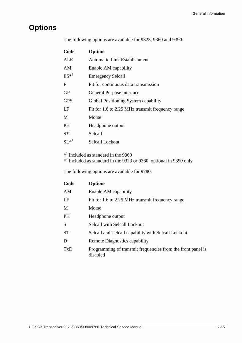
Options
The following options are available for 9323, 9360 and 9390:
Code Options
ALE Automatic Link Establishment
AM Enable AM capability
ES*1 Emergency Selcall
F Fit for continuous data transmission
GP General Purpose interface
GPS Global Positioning System capability
LF Fit for 1.6 to 2.25 MHz transmit frequency range
M Morse
PH Headphone output
S*2 Selcall
SL*1 Selcall Lockout
*1 Included as standard in the 9360*2 Included as standard in the 9323 or 9360, optional in 9390 only
The following options are available for 9780:
Code Options
AM Enable AM capability
LF Fit for 1.6 to 2.25 MHz transmit frequency range
M Morse
PH Headphone output
S Selcall with Selcall Lockout
ST Selcall and Telcall capability with Selcall Lockout
D Remote Diagnostics capability
TxD Programming of transmit frequencies from the front panel isdisabled


HF SSB Transceiver 9323/9360/9390/9780 Technical Service Manual 3-1
3 Brief description
This section of the manual provides a brief description of the major componentsand circuit functions of the 9323, 9360, 9390 or 9780 transceiver as follows:
• control and switching functions
• synthesiser operation
• receive path
• transmit path
For an in-depth review of these functions see chapter 4 , Technical description.

Brief description
3-2 HF SSB Transceiver 9323/9360/9390/9780 Technical Service Manual
General
Read this description of the 9323, 9360, 9390 or 9780 transceiver in conjunctionwith the Block Diagram 03-00902.
The 9323, 9360, 9390 or 9780 transceiver uses the same double conversion inReceive and Transmit modes. Only the 45 MHz band-pass filter, the 455 kHzsideband filter and the local oscillators VCO1 and VCO2 are common to bothmodes of operation. The signal routing is determined by switching and controlvoltages according to the mode selected.
The circuits and functions of the 9323, 9360, 9390 or 9780 are located on fourmajor PCBs as shown in Figure 3-1:
• Display panel PCB
• Microprocessor and audio PCB
Micro and I/O
Transmit audio
Receive audio and Selective call
• Rx/Exciter PCB
RF Mixer and synthesiser
455 kHz IF modulator and demodulator
• PA and Filter PCB
Microprocessorand Audio
DisplayPanel
Rx/Exciter PA and Filters
Figure 3 -1: 9323, 9360, 9390 and 9780 PCB block diagram

Brief description
HF SSB Transceiver 9323/9360/9390/9780 Technical Service Manual 3-3
Control and switching
Most of the transceiver functions are microprocessor controlled. The channelfrequencies are programmed via the microprocessor to the Electrically ErasableProgrammable Read Only Memory (EEPROM). The remaining facilities are pre-programmed in the Erasable Programmable Read Only Memory (EPROM).
The power On function is controlled by hardware and the power Off function iscontrolled by software. The rotary volume control is a digital contacting encoder.It controls a 16-step attenuator in the audio signal path between the preamplifier(after the demodulator) and the amplifier. This drives the loudspeaker.

Brief description
3-4 HF SSB Transceiver 9323/9360/9390/9780 Technical Service Manual
Synthesiser
The 9323, 9360, 9390 or 9780 transceivers use single loop synthesisers. The mainsynthesiser (VCO1) generates an oscillator frequency in 2 kHz steps. In receive,the oscillator frequency ranges from 45.250 MHz to 75 MHz. In transmit theoscillator frequency will depend on the transceiver type and the options fitted. Itwill be within the range of 46.6 MHz to 75 MHz.
The vernier synthesiser (VCO2) generates oscillator frequencies of 44.5435 MHzto 44.5455 MHz in 10 Hz steps.
The synthesisers are controlled by the same process that controls the remainder ofthe transceiver. Serial data representing the various pre-programmed channelfrequencies is loaded into both synthesisers.
When upper sideband is selected, the 9323, 9360, 9390 or 9780 uses a singlecrystal reference oscillator of 7304 kHz. The reference oscillator is also used toprovide the 456.5 kHz (7304 kHz divided by 16) signal for the audiomodulator/demodulator.
For lower sideband operation a separate crystal oscillator is selected, operating at1814 kHz to provide 453.5 kHz (1814 kHz divided by 4) to the audiomodulator/demodulator.

Brief description
HF SSB Transceiver 9323/9360/9390/9780 Technical Service Manual 3-5
Receive path
PA and Filter PCB
The received signal from the antenna passes through a PA low-pass filter, onto thetransmit/receive relay. It is then sent to the receiver input on the Rx/Exciter PCB.
Rx/Exciter PCB
From the receive input, the signal passes through a selected high-pass filter and isfed either directly to a 30 MHz low-pass filter or via an RF amplifier. The outputof the low-pass filter is fed to the input of the first balanced mixer. Here it mixeswith the local oscillator VCO1 to produce an IF signal centred on 45 MHz.
The 45 MHz signal is filtered using a 15 kHz wide band-pass filter before beingapplied to the second balanced mixer. The signal mixes with a second localoscillator VCO2 producing an IF signal centred on 455 kHz.
The output of the second mixer divides into two paths:
• the main path passes the signal through a noise gate to a 2.5 kHz sideband filterwhere only the wanted sideband passes to the high gain AGC controlled IFamplifier
• the second path passes the signal through an amplifier that detects noise andcontrols the noise gate to remove impulse noise, such as car ignition, from the455 kHz signal
The amplified 455 kHz signal is demodulated to produce an audio signal. It is thenamplified. The amplified audio signal operates an AGC circuit. This controls theIF amplifier gain to prevent overloading when receiving strong signals. It is alsoused to maintain a constant audio output with changing input signals.
The amplified audio signal is fed via a mute gate to the volume control. The mute,when enabled, removes the receiver noise from the speaker. When speech isdetected, the gate in the audio line closes to allow the signal to be heard.
The signal from the volume control is applied to a power amplifier IC to drive thetransceiver’s loudspeaker.

Brief description
3-6 HF SSB Transceiver 9323/9360/9390/9780 Technical Service Manual
Transmit path
Microprocessor and Audio PCB
The microphone audio is amplified and levelled in the microphoneamplifier/compressor, then fed to a balanced modulator.
Rx/Exciter PCB
When mixed with the local oscillator, the double sideband output of the modulatoris applied to a 2.5 kHz sideband filter centred on 455 kHz, passing only thewanted sideband to the first mixer. Here it mixes with the local oscillator VCO2 toproduce an IF signal centred on 45 MHz.
The transmit signal is filtered by the 15 kHz wide band-pass filter before being fedto the input of the second mixer.
At the second mixer, the signal mixes with the output of oscillator VCO1 toproduce the required channel frequency. It passes through a 30 MHz low-passfilter to the PA and Filter PCB.
PA and Filter PCB
On the PA assembly, the signal is amplified, then it is passed through thetransmit/receive relay to the selected band filter. The output from the filter is fedvia the VSWR detector to the antenna output connector. From here it is connectedby coaxial cable to the antenna.
The VSWR detector monitors the forward and reflected power and controls thepower output of the transmitter. If a high VSWR is detected, the power output isreduced to protect the PA.

HF SSB Transceiver 9323/9360/9390/9780 Technical Service Manual 4-1
4 Technical description
This section of the manual contains a technical description of the 9323, 9360,9390 or 9780 transceiver and 9330, 9366, 9391 or 9782 control head. It should beread together with the drawings in chapter 9, Drawings.
Control and supply voltages
All switching, except power On, is controlled either directly or indirectly by themicroprocessor IC101 (located on the Microprocessor and Audio PCB) inconjunction with the microprocessor IC2 in the control head.
Power on
1 04-02974When the On/Off button on the control panel is pressed, the PWR ON line (P4pin 3) is pulled low via the series circuit consisting of diode D1 on the On/Offbutton and D3.
The cathode of D3 is at 0 V prior to switch on, permitting the PWR ON line tomomentarily be held low by discharged capacitors on the 5 V rail.
1 04-02976 Sheet 2The PWR ON line on the front panel is connected via a short cable to P201 pin 3located on the Microprocessor and Audio PCB. From there it is fed via R222 tothe base of transistor V203.
1 04-02976 Sheet 2The PWR ON line from the extended control head is connected by a control cableto the transceiver rear panel connector P204 pin 4, then via a ribbon cable to theMicroprocessor and Audio PCB (P203 pin 7). From there it is fed through an RFsuppression network (L205 and C236) then connected in parallel to the frontPWR ON line, then via R222 to the base of V203.
With the PWR ON line low, V203 conducts and energises the ON coil of latchingrelay K201 resulting in contacts K201 closing and applying a ground to the TCVRON line.
The TCVR ON line is connected from the Microprocessor and Audio PCB viaP101 pin 3 (see Sheet 1) to P1 pin 3 on the PA assembly [1 04-02973 and04-03096] and finally to the negative side of relay K8.
If the polarity of the DC supply is correct and below 16 V, V4 will conduct andrelay K8 will energise, closing contacts K8-1 and connecting the DC supply to thetransceiver. The PWR ON line is disabled on start up when D3 on the control headis reverse biased by the 5 V supply.
Technical description
4-2 HF SSB Transceiver 9323/9360/9390/9780 Technical Service Manual
If the DC supply voltage exceeds 16 V, zener diode V2 conducts causing V3 toalso conduct and switch off V4, thus preventing K8 from energising.
Diode D7 prevents relay K8 from operating if the DC supply is reverse polarised.
The power input circuit is protected from high voltage transients by VoltageDependent Resistor (VDR) R8.
Power off
If the On/Off button on the control panel is pressed [1 04-02974] when thetransceiver is operational, a scanning active low pulse from the microprocessorIC2 pin 11 is applied to the input port of IC1. The interrupt line (pin 13)momentarily goes low, indicating to the microprocessor IC2 to read the input portsof IC1 and to switch off the transceiver.
The switch off command is sent from IC2 (pins 22 and 23) via the external I2Cbus to microprocessor IC101 on the Microprocessor and Audio PCB [104-02976 Sheet 1] pins 22 and 23.
Microprocessor IC101 outputs data on the local I2C bus to IC109 pins 23 and 24,latching pin 5 on the PWR OFF line low. The OFF coil of latching relay K201(see Sheet 2) energises, opening K201 contacts and releasing the power relay K8on the PA assembly, thus switching off the transceiver.
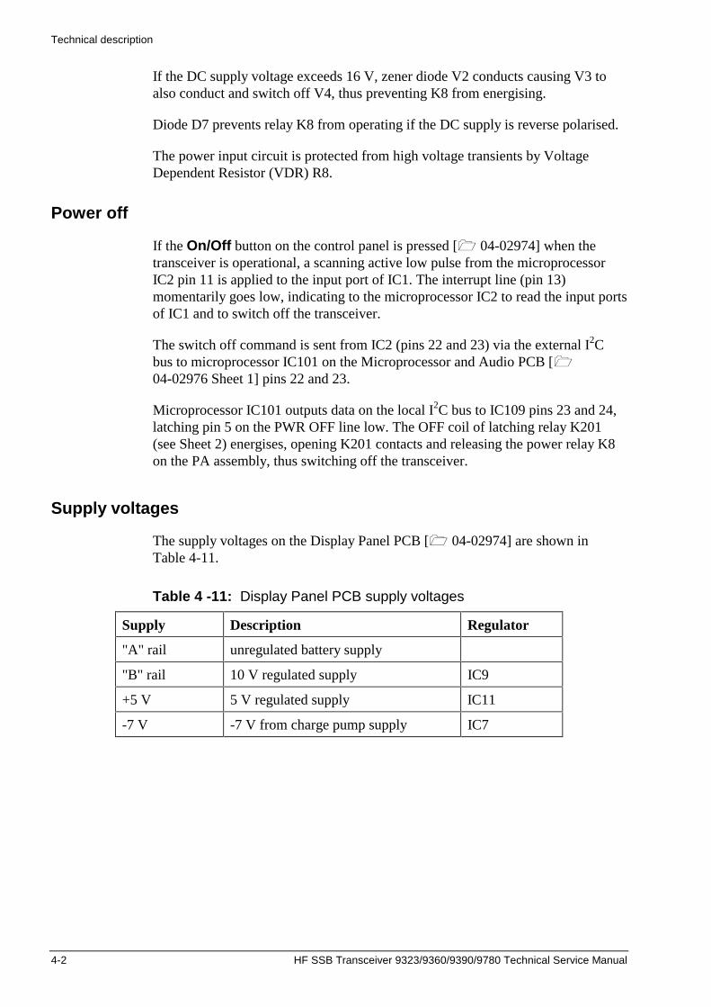
Supply voltages
The supply voltages on the Display Panel PCB [1 04-02974] are shown inTable 4-11.
Table 4 -11: Display Panel PCB supply voltages
Supply Description Regulator
"A" rail unregulated battery supply
"B" rail 10 V regulated supply IC9
+5 V 5 V regulated supply IC11
-7 V -7 V from charge pump supply IC7

Technical description
HF SSB Transceiver 9323/9360/9390/9780 Technical Service Manual 4-3
The supply voltages on the Microprocessor and Audio PCB [1 04-02976] areshown in Table 4-12.
Table 4 -12: Microprocessor and Audio PCB supply voltages
Supply Description Regulator
"A" rail unregulated battery supply
"B" rail 10 V regulated supply IC201
+5 VA 5 V regulated supply IC202
+5 VB 5 V regulated supply IC203
The supply voltages used on the Rx/Exciter PCB [1 04-02972] are shown inTable 4-13.
Table 4 -13: Rx/Exciter PCB supply voltages
Supply Description Regulator
"A" rail unregulated battery supply (suppliesthe crystal oven only)
"B" rail +10 V regulated supply IC201*
+5 VB 5 V regulated supply IC203*
+18/26 V 18 & 26 V from the charge pumpsupply
IC11
* Regulator is located on the Microprocessor and Audio PCB [1 04-02976]
The supply voltages on the PA and Filter PCB [1 04-02973 and 04-03096] areshown in Table 4-14.
Table 4 -14: PA and Filter PCB supply voltages
Supply Description Regulator
"A" rail unregulated battery supply
+5 V 5 V regulated supply selected intransmit only
IC2
+5 V 5 V supply (supplies IC1 only) V1

Technical description
4-4 HF SSB Transceiver 9323/9360/9390/9780 Technical Service Manual
Receive/Transmit switching
The main transmit/receive DC switching circuit originates from the latched outputof IC209 pin 6 located on the Rx/Exciter PCB [1 04-02972 and 04-03135Sheet 2]. IC209 pin 6 is connected to two transistors V209 and V212. V209governs the AGC function. V212 forms part of the circuit controlling the transmitand receive mixer circuits.
When the Receive mode is selected, the output of IC209 pin 6 is latched to 0 V,switching V209 off and allowing the AGC to function normally. V212 is alsoswitched off, allowing the first NAND gate of IC6/D to be pulled high by resistorR42. This sets the output of IC6/D pin 11 low, switching on V2 and V6, thusenabling the receive mixers IC4 and IC7. The output of the second NAND gateIC6/C will go high, switching V3 and V7 off and inhibiting the transmit mixersIC5 and IC8.
When the PTT inputs are detected by the microprocessor IC101 [1 04-02976Sheet 1] it sends a command via the local I2C bus to IC209 [1 04-02972 and04-03135 Sheet 2] to latch the output pin 6 high (+5 V). This causes V209 in theAGC circuit to conduct, setting the AGC to 0 V and disabling the 455 kHz IFamplifier. Resistor R255 provides a small DC offset to IC205/A to ensure theAGC always switches to 0 V.
With IC209 pin 6 latched high, V212 conducts, setting the input of IC6/D pin 13low. This in turn sets the output of IC6/D pin 11 high, thus switching off V2 andV6, disabling the receive mixers IC4 and IC7 and providing the DC voltage toenable the transmit mixers IC5 and IC8.
The noise limiter in Transmit mode is disabled by V7 conducting, thus applying aDC level via D201 and R203 (see Sheet 2) to the AGC input pin of noiseamplifier IC201 pin 5.
DC from V7 has two other functions. It provides bias via R238 to IC202 pin 5 toenable the modulator. It also biases V5 (see Sheet 1) on, clamping the base of V4to 0 V, thus preventing D19 from conducting and attenuating the transmit signal.
Serial data from the microprocessor IC101 [1 04-02976 Sheet 1] is also appliedto IC1 on the PA assembly. When transmit is selected, a ground on pin 12energises the transmit/receive relay K7. The path is now completed from the PAoutput to the antenna.
In Transmit mode, the microprocessor IC101 outputs a low from pin 28. This isapplied to the input of inverter buffer IC207 pin 12 (see Sheet 2). The high at theoutput pin 14 is connected to:
• the antenna control connector P202 pin 15
• the optional PCB output P204 pin 12
• the mute squaring amplifier IC307/B via R365 and D307 (see Sheet 3)
The DC applied to IC307/B applies a small offset to disable the squaring amplifierduring transmission.

Technical description
HF SSB Transceiver 9323/9360/9390/9780 Technical Service Manual 4-5
Receiver
Input low-pass filters
1 04-02973 and 04-03096The receiver input signal is fed through one of six relay-selected, PA Low-PassFilters (LPF) K1–K6. The signal is then fed via the transmit/receive relay K7 andsignal clamping diodes D3–D6 to connector J3.
High-pass filters
1 04-02972 and 04-03135 Sheet 1From J3 on the PA assembly, the High-Pass Filter (HPF) is connected by a coaxialcable to J2 located on the Rx/Exciter PCB. Six HPFs are used to complete theband-pass filter (BPF) characteristics. These are diode switched according to thefrequency band in use, by grounding the appropriate select line from IC1. Forbroadcast channels below 2 MHz, a 14 dB resistive attenuator is selected insteadof a filter.
This is an example of how the HPF works. If the HPF 2-3.1 is selected, IC1 pin 10switches from 10 V to 0 V. This completes the input DC switching current pathfrom the "B" rail via R2, L1, D11, L18 and R14 to 0 V. Diode D11 is forwardbiased and passes the receive signal to the input of the selected HPF.
The output DC switching current path from the "B" rail consists of R3, L2, D12,L20 and R15 to 0 V. With D12 forward biased, the receive signal at the output ofthe 2-3.1 HPF can either be fed directly via D15 and C57 to the following 29 MHzlow-pass filter (LPF) or via D16 to the input of the RF amplifier.
RF amplifier
1 04-02972 and 04-03135 Sheet 1The RF amplifier (consisting of V1 and its associated components) has a nominalgain of 12 dB. It can be selected from the front panel on the control head. Whenthe RF amplifier is selected, IC2 pin 12 goes high, switching the output of IC3/Aand B (in parallel) from 0 V to approximately 10 V. This action applies DC voltsvia RF filter inductor L27 to the primary of T2, then to the series inductors of theLPF L26-L24 to the collector of V1. The DC volts also forward biases V1 viafeedback resistor R24.
With the RF amplifier selected, the voltage on the base of V1 is positive withrespect to the output of the HPF network, thus forward biasing D16. This allowsthe signal to pass to the input of the RF amplifier. At the same time, D15 isswitched off, as the cathode is held approximately 2 V positive with respect to theanode.

Technical description
4-6 HF SSB Transceiver 9323/9360/9390/9780 Technical Service Manual
LPF and first mixer
1 04-02972 and 04-03135 Sheet 1The output from the HPF is fed direct, or via the RF amplifier, to a 29 MHz LPF(C59, L24, C60/61, L25, C62, & L26) and then via transformer T2 to the balancedinput of the first mixer IC4 pins 12 and 13.
Mixer IC4 is a combined amplifier/balanced mixer with a gain of approximately20 dB. The received signal is mixed with the output of the Voltage ControlledOscillator (VCO1), then applied to pin 5. This operates between 45.250 MHz and75 MHz to produce a balanced IF output (pins 3 and 14) centred at 45 MHz.
DC is applied to the mixer IC4 pins 3 and 14 via the filtered "B" rail and thecentre tap of the mixer output transformer T3. In Receive mode, V2 is conductingand supplies the filtered "B" rail to IC4 pin 4 and 11, via R34 and R36respectively.
45 MHz band-pass filter
1 04-02972 and 04-03135 Sheet 1The 45 MHz IF signal is filtered through a 15 kHz BPF (centred on 45 MHz)consisting of T3, Z1, L30, Z2 and T4. This removes unwanted signals produced bythe first mixer. The filtered output is applied via coupling capacitors C84 and C85to the balanced input of the second mixer IC7 pins 12 and 13.
Second mixer
1 04-02972 and 04-03135 Sheet 1Mixer IC7 is a combined amplifier/balanced mixer and identical to mixer IC4.The 45 MHz signal is mixed with the output of the second Voltage ControlledOscillator (VCO2), then applied to pin 5. This operates between 44.5435 MHzand 44.5455 MHz to produce a second IF centred at 455 kHz.
DC to the mixer output is provided by the filtered "B" rail, which is connected tothe centre tap of the 455 kHz output transformer T201 (Sheet 2). It is then fed tothe mixer output transformer T3. In Receive mode when V6 is conducting, the "B"rail provides DC via R45 to IC7 pin 4 and bias via R47 to pin 11.
Noise limiter
1 04-02972 and 04-03135The 455 kHz output of IC7 pins 3 and 14 is applied via C201, R201, C202 andR202 to the balanced input of a high gain amplifier IC201 pins 4 and 6.
The balanced outputs at pins 1 and 8 are connected to a tuned auto transformerT202 (455 kHz). The output of T202 is applied to the base of V201, which is anactive rectifier. Noise bursts produce positive going pulses at the collector ofV201 and trigger, via V202, the monostable flip-flop IC6A/B. The pulse width isdetermined by C208 and R210 (nominally 250 µs).

Technical description
HF SSB Transceiver 9323/9360/9390/9780 Technical Service Manual 4-7
The outputs of the flip-flop pins 3 and 4 produce complimentary pulses that areconnected to the FET gates of V204 and V205. These gate out the noise burstsfrom the 455 kHz signal. With V204 on and V205 off, the IF signal is passed tothe sideband filter Z202. When a noise burst is present, V204 is switched off andV205 is switched on, blocking the IF signal for the period of the gate pulse.
The average DC component of V201’s collector current is used as an automaticgain control to IC201. It is applied via R206 to pin 5. This ensures that only thenoise burst signal triggers the monostable. The AGC decay constant is set by thecomponents C204 and R205.
In transmit, IC201 is disabled (see page 4-4, Receive/Transmit switching).
455 kHz filter and IF amplifier
1 04-02972 and 04-03135 Sheet 2The IF signal from the noise blanker gate V204 is applied to a 2.5 kHz ceramicfilter Z202. The filter removes the unwanted sideband, adjacent channels andother unwanted products generated by the second mixer. The wanted sideband,centred at 455 kHz, is passed by the filter to a two-stage gain controlled amplifier,consisting of V207, V208, and its associated components.
The IF amplifier is broadly tuned to 455 kHz by the tuned circuits L202/C219 andL203/C223.
Demodulator
1 04-02972 and 04-03135 Sheet 2The output of the 455 kHz IF amplifier is passed via coupling capacitor C224 tothe input of a double balanced mixer IC203 pin 1. The IF signal is mixed with thelocal oscillator that is applied to pins 8 and 10 to produce an audio output at IC203pin 6. The local oscillator operates at 456.5 kHz for USB conversion and453.5 kHz for LSB. For details of operation of the local oscillator see page 4-18,455 kHz local oscillator for USB/LSB.
© Local oscillators VCO1 and VCO2 shift by a total of 3 kHz when switching fromUSB to LSB. This enables filter Z202 to be used for either sideband.
Automatic gain control
1 04-02972 Sheets 1 and 2An Automatic Gain Control (AGC) is applied to a number of stages in thereceiver. This is used to increase the dynamic range of the receiver and to maintainan almost constant audio output level for a large variation of input signals.
When the receiver is at maximum gain, the AGC at the output of IC205/A pin 1(TP205) (see Sheet 2) is nominally 5.5 V. This is set by the resistor divider R257and R258 in conjunction with the gain setting resistors R254 and R259.

Technical description
4-8 HF SSB Transceiver 9323/9360/9390/9780 Technical Service Manual
The demodulated audio output from IC203 is first amplified by IC204/A thenpassed via a resistive attenuator (R263 and R264) to a full wave active peakrectifier circuit V210 and V211.
Under no signal conditions, IC204/A output, V210 and V211 bases and emittersare all at the same potential of 5 V. When the audio swing at the output of IC204exceeds approximately ±0.75 V (from 5 V), it causes V210 to conduct during thepositive peaks and V211 during the negative peaks. The common collector outputcharges capacitor C237 during the transistor’s conducting period. The resultingDC is applied to inverting amplifier IC205/A causing the AGC output to drop to alevel determined by the strength of the received signal. This lowers the voltageapplied to gate 2 of both FETs V207 and V208, reducing the overall gain of the455 kHz IF amplifier.
AGC is applied to a second inverting amplifier IC204/B to extend the dynamicrange of the receiver. Its output produces an inverted AGC, nominally 0 V under ano signal condition, but starts to rise once the input to IC204/B falls below 3.2 V(set by R249 and R250).
The inverted AGC from IC204/B is divided into two paths:
• one path is connected via R223 to gate 1 of V207, improving the gain controlof the 455 kHz IF amplifier
• the second path is via a delay and damping network (R221/V206, R220, C215,D203, and R41) to the base of V4 (see Sheet 1)
The pin diodes D19 across the first mixer output act as variable resistors. Theresistance falls as V4 collector current increases with a rise in AGC, thus reducingthe mixer output gain at high signal levels.
Another AGC circuit is incorporated at the output of the second mixer. It is usedfor signals that are out of the 2.5 kHz sideband frequency, but within the 15 kHzBPF bandwidth (see Sheet 1). V15 is connected between one side of the balancedoutput and the "B" rail. When the output swing from the mixer IC7 exceeds 0.7 Vbetween the base and the rail, V15 conducts and reduces the gain of the first mixerby increasing the current through the pin diodes D19.
The AGC fast attack time is set by R262, R263 and R264 in the emitter circuit ofthe peak rectifiers V210 and V211 (see Sheet 2). Capacitor C237 charges and theresultant slow decay time of C237 is through the resistor network R260 and R259.The attack and decay time will vary at different signal strengths, but nominally areabout 2 ms and 0.5 s respectively. Resistor/diode networks R276/D207 andR277/D208 are connected to outputs on IC209 (pins 4 and 5) and can begrounded, under software control. This reduces the AGC decay time constantwhen required for special applications.

Technical description
HF SSB Transceiver 9323/9360/9390/9780 Technical Service Manual 4-9
Voice mute
1 04-02976 Sheets 1, 2 and 3The audio at the output of IC204/A on the Rx/Exciter PCB [1 04-02972Sheet 2] is connected via P201 pin 9 (Rx Audio) to the Microprocessor and AudioPCB pin 9 (see Sheet 2). It is then coupled via C206 to the input of IC307A (seeSheet 3), which operates as a squaring amplifier. At the open collector output, thesquared signal across load resistor R352 charges C343 via D308 during thenegative excursions. The charge is transferred to C344 by V303 during thepositive excursions. The resultant DC voltage on C344 is proportional to thefrequency of the audio (i.e. voltage rises as frequency increases). The squaringamplifier is disabled in transmit by applying a DC offset from IC207 pin 14(Sheet 2) via D307 and R365 to IC307/B pin 5.
IC304/B and its associated components function as an LPF with a cut-offfrequency of approximately 10 Hz. The output from IC304/B is a DC voltagevarying at the syllabic rate of the received speech.
IC307/C and IC307/D form a window comparator. The window width is adjustedby the mute sensitivity preset R357. The divider network R359 and R360 togetherwith C348 averages the output of IC304/B to provide the reference voltage for thewindow comparator. If the output from IC304/B rises or falls below this referenceby the amount set by R357, then the open collector outputs of IC307/C andIC307/D will discharge C349, applying a low to the input of comparator IC307/Bpin 6.
The second input of comparator IC307/B pin 7 is set to 4 V by resistor dividerR363 and R364. When input pin 6 falls below 4 V, the comparator output at pin 1goes high (MUTE DET line). This indicates to the microprocessor IC101, viaIC111 pin 5 (see Sheet 1), that speech has been detected.
Mute detection timing is controlled by discharging C349 through R361 for a fastattack and charging C349 via R362 for a slow release (about 3 seconds).
When Voice Mute mode is selected by the Voice Mute button on the controlpanel [1 04-02974], the microprocessor IC2 on the control head sends a signalvia the external I2C bus to the microprocessor IC101 on the Microprocessor andAudio PCB [1 04-02976 Sheet 1]. The microprocessor IC101/A sends acommand via the local I2C bus to IC114 to latch the mute switch pin 19 low. Thisapplies a low to IC206/D pin 12 (see Sheet 3), which opens the mute gate and onlyallows a very low level of audio to pass via R330 (when fitted) to the volumecontrol circuit.
When voice is detected by the mute circuit, a high is applied to IC111 pin 5(MUTE DET line). The interrupt pin (pin 13) momentarily goes low, informingthe microprocessor to read the input ports of IC111. This will indicate to themicroprocessor that the mute detect line is high. The microprocessor then sets themute switch IC114 pin 19 high and closes the mute gate IC206/D (see Sheet 3).The audio is then passed to the volume control circuit.

Technical description
4-10 HF SSB Transceiver 9323/9360/9390/9780 Technical Service Manual
Volume control and audio output amplifier
1 04-02974, 04-02976 Sheets 1 and 3The volume control circuit is a 16-step attenuator and consists of R334–R340.Each step has ≈4 dB of attenuation, giving a total of 64 dB.
The rotary volume control is a digital contacting encoder. When this control isrotated in either direction, the microprocessor IC2 on the Display Panel PCB [104-02974] reads each position change. It sends commands via the external I2C busto the microprocessor IC101 on the Microprocessor and Audio PCB (see Sheet 1)to select the appropriate audio attenuators. The microprocessor IC101 then sendsdata via the local I2C bus to change the output ports of IC114 pins 3–6. This actioncontrols the analogue switches that switch the step attenuator in and out.
The audio is passed from the buffer amplifier IC304/A, through a resistorattenuator R342 and R343, to the input of the loudspeaker amplifier IC306.
The maximum output of the audio amplifier is either:
• 2.5 W into an 8 Ω speaker
• 8 W into a 2 Ω speaker
Warning beeps are heard if the maximum or minimum limits of the volumecontrol are reached. The warning beeps are generated from the tone generatorIC106 pin 10 [1 04-02976 Sheet 1]. The tone is fed via a resistor attenuatornetwork to the input of the loudspeaker amplifier IC306 (BEEPS I/P line). Thebeep audio level is varied by the volume control. The level is controlled by themicroprocessor, which selects the appropriate attenuator shunt resistors (R138,R140 and R142) to ground (IC109 pins 8, 9 and 10).
Low voltage Tx inhibit
1 04-02972 and 04-03135 Sheet 2The comparator IC211A on the Rx/Exciter PCB monitors the "A" rail. When thesupply voltage drops to 9 V, the output of IC211A is pulled low thus disabling thePTT line connected from IC209 pin 6 via R275 to transistor switch V212. Thisfunction prevents the transceiver latching in Tune mode when the supply voltagedrops below 9 V.

Technical description
HF SSB Transceiver 9323/9360/9390/9780 Technical Service Manual 4-11
Transmitter exciter
Microphone amplifier/compressor
1 04-02974 and 04-02976The microphone insert is a moving coil device and is active when the PTT buttonis pressed. This removes the short circuit across the microphone, and at the sametime, applying a ground to the PTT line on J1 pin 5.
The microphone is connected to the control panel via J3 pins 2 and 3 [104-02974] and to the PCB via P3 pins 1 (ground) and 5. From there, themicrophone audio is passed through an RF filter network R24 and C21 to theinput of the preamplifier IC10/B.
When the microphone is not in use, the input switch (consisting of transistor V10and associated components) disables the audio by applying a short across theinput.
The audio output of amplifier IC10/B is fed through an RF decoupling network(R40, C41 and R44) to connector P4 pin 2. In the front panel control version, theaudio is connected to P201 pin 2 on the Microprocessor and Audio PCB [104-02976 Sheet 2). From there it is fed via capacitor C219 and analogue switchIC206/A to the combining amplifier IC204/A.
For the control head version, the Tx audio at connector P4 pin 2 is fed via acontrol cable to P204 pin 11 on the transceiver. From there the output is connectedvia a ribbon cable to P203 pin 6 on the Microprocessor and Audio PCB [104-02976 Sheet 2]. The audio path continues from pin 6 via a second RFsuppression network (R229/B and C242), through C218 and analogue switchIC206/C to the combining amplifier IC204/A.
Additional audio inputs are applied to the combining amplifier IC204/A from:
• the tone generator IC106 via R213
• the optional PCB (P204 pin 3) via R214
• the option PS input (P303 pin 5) via C217, analogue switch IC206/B and R216
The microphone audio at the output of IC204/A is applied to the input of amicrophone compressor amplifier consisting of IC204/B, IC205/A and B, V202and associated components. This provides a constant output for a large variationin speech levels applied to the input (≈30 dB range).
When there is no speech present, the amplifier IC204/B is set to the maximumgain. This is determined by the feedback resistor R208 and the shunt FET V202,which functions as a variable resistor (minimum resistance is ≈150 Ω formaximum gain).
The output of amplifier IC204/B is connected to the inputs of IC205/A andIC205/B forming a window comparator. The window is set by the divider chainR204–R207 to be centred at 5 ±0.25 V.

Technical description
4-12 HF SSB Transceiver 9323/9360/9390/9780 Technical Service Manual
When the level of the speech input applied to the microphone amplifier is greaterthan ≈3.5 mV P (compression threshold), the output swing will exceed thecomparator window (±0.25 V). This produces negative going output pulses fromthe comparator IC205/A and B pins 1 and 7. These pulses lower the DC charge oncapacitor C212. The effect is that the voltage will be reduced on the FET gate ofV202. This increases the resistance of the FET and lowers the gain of themicrophone. This puts the microphone amplifier into compression. The outputlevel remains constant for a further 30 dB increase in input level beforeoverloading occurs.
Under normal speech conditions, the time constant (consisting of C212 andR211), sets the talk power ratio and produces a high average transmission powerlevel. When data transmission is required, the time constant is extended byswitching in capacitor C213 in parallel to C212 (TALK PWR OFF line). This isachieved by a command from the microprocessor IC101 [1 04-02976 Sheet 1] toset the output port of IC114 pin 10 low, thus grounding the negative side of C213.
When lower power is required for CB channels, the drive level to the PA isreduced by the microprocessor IC101 setting IC114 pin 9 low. This causes FETV201 (see Sheet 2) to switch on and apply R203 in parallel to resistors R205 andR206. This action reduces the comparator window to ±0.125 V, resulting in areduction of 6 dB in the audio output from the microphone compressor amplifierIC204/B.
Modulator
1 04-02972 and 04-03135 Sheet 2The transmitter audio output of IC204/B is passed via P102 pin 4 to theRF/Exciter PCB P201 pin 4. The output is then fed to the input of the balancedmodulator IC202 pin 1. The modulator is enabled when DC is applied via thetransistor switch V7 and R238 (Sheet 1) to the bias input pin 5.
The audio is mixed with the local oscillator of 456.5 kHz (453.5 kHz for LSB)and is applied to pin 8 and 10 (see page 4-18, 455 kHz local oscillator forUSB/LSB). This produces a DSB output at pin 6. From there it is passed via D204to the 455 kHz sideband ceramic filter Z202 pin 1.
455 kHz filter and first mixer
Filter Z202, with a bandwidth of 2.5 kHz, filters out the unwanted sidebandleaving only the wanted sideband at pin 3. From there it is fed via the noise limitergate V204 (disabled in transmit) to a tuned auto transformer T201. It is fed fromT201 via a resistor matching attenuator network R48 and R49 [1 04-02972 and04-03135 Sheet 1] to the input of the first balanced amplifier/mixer IC8 pins 12and 13.
The first mixer IC8 (see Sheet 1) is enabled by operating transistor switch V7,applying DC via R46 to pin 4 and bias current via R50 to pin 11. The filtered "B"rail is applied to the mixer output pins 3 and 14 via the centre tap of outputtransformer T4.

Technical description
HF SSB Transceiver 9323/9360/9390/9780 Technical Service Manual 4-13
In the first mixer IC8, the 455 kHz transmit signal is mixed with the output of thelocal oscillator VCO2. This is applied to pin 5 to produce a second IF outputsignal centred on 45 MHz (pins 3 and 14). The gain of the mixer/amplifier isapproximately 20 dB.
45 MHz band-pass filter
The 45 MHz IF signal is filtered through a 15 kHz BPF consisting of T4, Z2, L30,Z1 and T3. This removes unwanted signals produced by the first mixer. Thefiltered output is applied to the balanced input of the second mixer IC5 pins 12and 13.
Second mixer and exciter output filter
The second mixer IC5 is enabled by operating the transistor switch V3. Thisapplies DC through R35 to pin 4 and bias current via R38 to pin 11. The filtered"B" rail is applied via preset resistor R22 and transformer T1 to the mixer outputpin 3 and 14.
The 45 MHz transmit signal is mixed with the output of local oscillator VCO1then applied to IC5 pin 5 to produce the selected channel frequency at the mixeroutput (pins 3 and 14). The gain of the mixer/amplifier is approximately 20 dB.
The balanced network, consisting of components R22, C55 and C56, is adjusted toremove unwanted spurious signals.
The mixer output is fed via a 29 MHz low-pass filter (consisting of L23, C53,C51/52, L21 and C50) to the transmit exciter output connector J1. From there it iscoupled via a coaxial cable to the PA assembly.
Tune
When the Tune button is pressed [1 04-02974], a low is applied to the inputport of IC1. The interrupt pin (pin 13) momentarily goes low indicating that themicroprocessor IC2 has to read the input port of IC1. It also detects that the Tunebutton has been pressed. The tune command will be sent via the external I2C busto the microprocessor IC101 on the Microprocessor and Audio PCB [104-02976 Sheet 1].
The microprocessor IC101 outputs data on the local I2C bus to IC209 on theRx/Exciter PCB [1 04-02972 and 04-03135 Sheet 2] to latch output at pin 6high and pin 10 low.
The high on IC209 pin 6 enables the transmit mixers and disables all of thereceive functions (see page 4-4, Receive/Transmit switching).

Technical description
4-14 HF SSB Transceiver 9323/9360/9390/9780 Technical Service Manual
The output pin of IC209 pin 10 is connected to a NOR gate IC206/A pin 2. Whenpin 2 is low, the 456.5 kHz carrier (453.5 kHz for LSB), which is always presentat IC206/A pin 3, then appears at the output (pin 1). This applies the carrier signalvia the driver transistor V203 to the input transformer T201 of the first transmittermixer IC8.
The output pin of IC209 pin 10 (see Sheet 2) is also connected to the input of theNOR gate IC206/D pin 11. When pin 11 is low, the output (pin 13) is set high,biasing V202 into saturation. The output of the second cascade NAND gate IC6/Bpin 4 goes low, opening the FET gate V204. This stops the re-inserted carrier frombeing loaded by the sideband filter Z202.
The carrier appearing at the output of the second mixer IC5 will be at thefrequency of the selected channel (SCF) and is used for tuning automatic andmanual antennas.

Technical description
HF SSB Transceiver 9323/9360/9390/9780 Technical Service Manual 4-15
Local oscillators
General
1 04-02972 and 04-03135 Sheet 1Two digitally controlled synthesised local oscillators are used to drive both thetransmit and receive functions of the first and second mixers. VCO1 operatesbetween 45.25 MHz and 75 MHz, moving in 2 kHz steps. VCO2 operates in therange of 44.5435 MHz to 44.5455 MHz, moving in 10 Hz steps.
The synthesisers IC10 and IC13 are programmed in serial data format from themicroprocessor IC101 [104-02976 Sheet 1], which accesses the channel datastored in the E2PROM memory.
Each synthesiser is locked to the reference oscillator. This consists of a7.304 MHz crystal (Z3) held at a constant temperature by an oven, which is one ofthe following:
• a PTC thermistor (E1) at 60°C
• a high stability oven [1 04-03095] where the R3 NTC resistor measures thetemperature of the crystal and causes the op-amp comparator IC1 to vary thecurrent in the heating element V2 to maintain the temperature of 65°C to within ±1°C
The temperature of the high stability oven is set by R4. V1, R12 and R13 limit themaximum current through V2 to approximately 400 mA.
VCO1 and phase lock loop (04–02972)
1 04-02972 Sheet 1The oscillator VCO1 is designed around a differential amplifier consisting ofFETs V8 and V9. The frequency of oscillation is determined by the tuned circuitL33, C94 and the capacitance of the varicaps D20 to D23. The oscillator outputpower is set by source resistors R55 and R58. The resistor R54 assists inmaintaining a constant output level over the operating frequency range.
The oscillator output at the tap of the tuned inductor L33 is coupled via C101 toan emitter follower V10. The output drives the two mixers IC4 and IC5 and theprescaler IC9 (all pin 5).
The high frequency output from VCO1 is divided by a 64/65 prescaler IC9, downto a frequency range of 706 kHz to 1.17 MHz (pins 2 and 3). A high or low onpin 1 sets the division ratio.
IC10 is a complex chip that contains two programmable dividers and a phasecomparator. The phase comparator compares two input signals of the samefrequency and outputs a voltage that is dependent on their relative phase.
Technical description
4-16 HF SSB Transceiver 9323/9360/9390/9780 Technical Service Manual
The input to comparator pin 4 is from the prescaler IC9. This is divided down to2 kHz by one of the programmable dividers. The quartz crystal (Z3) connectedbetween pins 7 and 8 forms the reference oscillator. It is set to a frequency of7304 kHz. The second divider is programmed to always divide the referencefrequency down to 2 kHz.
The two divided signals are applied to the phase comparator internal to IC10.When the two signals are "locked" in phase, the comparator output (pin 1) is atmid-rail (2.5 V). These two frequencies are locked together by the action of theloop, e.g. changing the first programmable divider will change the VCOfrequency.
Two separate outputs are available from the phase comparator. The output of IC10pin 2 (PDB line) is a course control that outputs a mark:space ratio proportional tothe frequency difference between the divided signals. The output of IC10 pin 1(PDA line) is the fine control. It gives an analogue output that takes over from thePDB output when the two signals are close to phase lock.
The transistors V11, V12, V13 and associated components form the loop filter.The input at the base of V13 is biased to 2.5 V by H1 (functioning as a zenerdiode). The output DC, which can swing between ground and the positive rail(26 V), is applied via L32 to the varicaps D20 to D23.
The components L32 and C95 provide an LPF to the control DC while presentinga high impedance to the oscillator circuit. The control DC level changes thecapacity of the varicaps to set the VCO to the required frequency. As the controlvoltage rises so does the frequency of the VCO.
When a new channel is selected, the microprocessor changes the value of theprogrammable divider IC10, which is fed by the prescaler IC9. As the two signalsdriving the phase comparator are now no longer at the same frequency, the phasecomparator outputs pulses to the loop filter. The output of the loop filter ramps inthe direction necessary to re-establish lock.
VCO1 and phase lock loop (04-03135)
1 04-03135 Sheet 1The oscillator VCO1 is designed around a differential amplifier consisting ofFETs V8 and V9. The frequency of oscillation is determined by the tuned circuitL33, C94 and the capacitance of the varicaps D20 to D23. The oscillator outputpower is set by source resistors, R55 and R58. The resistor R54 assists inmaintaining a constant output level over the operating frequency range.
The oscillator output at the tap of the tuned inductor L33 is coupled via C101 toan emitter follower V10. The output of V10 drives two mixers IC4 and IC5 viaC76 and C78 and a second emitter follower V11. The output of V11 is applied viaC104 and R66 to the input of synthesiser IC9 pin 4.
Synthesiser IC9 generates a DC control voltage via the phase/frequency detectorand control amplifier. This is applied to the varicaps to lock VCO1 to thenominated frequency.

Technical description
HF SSB Transceiver 9323/9360/9390/9780 Technical Service Manual 4-17
The 7304 kHz oscillator (part of IC9) is divided down to a 2 kHz referencefrequency. The VCO signal applied to IC9 pin 4 is also divided to produce 2 kHzwhen at the nominated frequency. Both of these signals are applied to thephase/frequency detector in IC9.
The phase/frequency detector provides two outputs. Pin 15 provides a "go down"pulse. Pin 14 provides a "go up" pulse. When locked, these outputs are high(+5 V) except for a very narrow low pulse that occurs simultaneously on bothoutputs.
V13 and V16 provide a 3 mA discharging current pulse whilst IC9 pin 15 is low.V12, V18, and V17 provide a 3 mA charging current pulse whilst pin 14 is low.
These current pulses accumulate in the loop filter (C106, C107, C151 and R70).The resulting voltage is applied to the varicaps (D20 - D23) via a filter (R51 andC96). This filter removes any reference signals from the control voltage.
VCO2 and phase lock loop (04-02972)
1 04-02972 Sheet 1The tuned circuit L40, C130/131, C132 and C133 sets the appropriate frequencyof operation. The network (consisting of C128, Z4, D31 and L39) is equivalent toa voltage controlled, very high Q series tuned circuit. This network effectivelygrounds the gate of V14 at the series resonant frequency. This determines the finalfrequency of oscillation.
The oscillator drive output from capacitor divider C132 and C133 is applied tomixers IC7 and IC8 and the prescaler IC12 (all pin 5).
The phase locked loop (PLL) incorporates VCO2. It works in a similar manner tothe phase locked loop that incorporates VCO1. The only exceptions are that thephase detector output (IC13 pin 17) is required to drive the loop amplifier IC14/Aand that the phase comparator varies from 1.1 kHz to 2 kHz. This allows the phasecomparator frequency to vary, enabling the loop to move in 10 Hz steps while stillhaving a relatively high phase comparator frequency.
The 7304 kHz reference oscillator output from IC10 pin 8 is applied to the PLLIC13 pin 2.
The DC output of the loop filter IC14/A pin 1 is applied via L36 to the varicapD31. It controls the frequency of the VCO. Components L36, R80 and C127, forman LPF to control the DC, while presenting a high impedance to the oscillatorcircuit. Component IC14 is powered from the 18 V output of the charge pumppower supply IC11 and associated components.

Technical description
4-18 HF SSB Transceiver 9323/9360/9390/9780 Technical Service Manual
VCO2 and phase lock loop (04-03135)
1 04-03135 Sheet 1VCO2 is a crystal controlled Colpitts oscillator. The tuned circuit L40, C130/131,C132 and C133 sets the appropriate frequency of operation. The network(consisting of C128, Z4, D31 and L39) is equivalent to a voltage controlled, veryhigh Q series tuned circuit. This network effectively grounds the gate of V14 atthe series resonant frequency. This determines the final frequency of oscillation.
The oscillator drive output, from capacitor divider C132 and C133 is applied tomixers IC7 and IC8. It is also applied via emitter follower V19 to the input ofsynthesiser IC10 pin 4.
Synthesiser IC10 is almost identical to VCO1 synthesiser IC9 except for thefollowing:
• The programmed division ratio of both the VCO and the reference frequenciesvary between 1.1 kHz to 2 kHz. A look up table contained on theMicroprocessor and Audio PCB allows for 10 Hz steps over the frequencyrange.
• Different filter components are used (C142, R110 and C141) because of thenarrower operating frequency range.
• The control voltage at the output of V23 and V24 are connected via sourcefollower V25 to varicap D31 of VCO2.
• The reference frequency is obtained from IC9 pin 2 via a buffer amplifier V26to IC10 pin 1.
455 kHz local oscillator for USB/LSB (04-02972)
In USB mode, the 7304 kHz reference oscillator is taken from the second PLLIC13 pin 3 [1 04-02972 Sheet 1]. It is then applied via a harmonic filter network(R268, C244, L205 and C245) [1 04-02972 Sheet 2] to the input of a "divide bytwo" divider IC208/A pin 3. The output (pin 6) is applied to a second "divide bytwo" divider IC208/B pin 11.
The enable line of dividers IC208/A and IC208/B pins 4 and 10 and the gate inputof IC206/C pin 8 are all connected to the output port of IC209 pin 9. In USBmode, the microprocessor IC101 [1 04-02976] latches the output of IC209 pin 9high, via the local I2C bus to IC209. This enables the dividers and disables the1814 kHz oscillator NOR gate IC206/C.
The 1826 kHz reference signal (7304 kHz divided by 4) of IC208/B pin 8 is fedvia NOR gate IC206/B to two more cascade "divide by two” dividers IC207/A andB. This produces a balanced output signal of 456.5 kHz signal at pin 8.
From here it is applied via the attenuator network (R269, R270, R271 and R272)to the balanced local oscillator inputs of modulator IC202 and demodulator IC203pins 8 and 10.
Technical description
HF SSB Transceiver 9323/9360/9390/9780 Technical Service Manual 4-19
In LSB mode, the microprocessor IC101 latches the output of IC209 pin 9 low.This disables the dividers IC208/A and B and enables the 1814 kHz crystaloscillator IC206/C . The signal is then fed via the NOR gate IC206/B and thedividers IC207/A and B (used for USB) to the modulator and demodulator. Thisproduces the required local oscillator frequency of 453.5 kHz.
455 kHz local oscillator for USB/LSB (04-03135)
In USB mode, the 7304 kHz reference oscillator is taken from the secondsynthesiser IC10 pin 3 [1 04-03135 Sheet 1]. It is then applied via a harmonicfilter network (R268, C244, L205 and C245 [1 04-03135 Sheet 2]) to the inputof the first "divide by two" divider IC208/A pin 3. The output (pin 6) is applied tothe second "divide by two" divider IC208/B pin 11.
The enable line of dividers IC208/A and IC208/B pins 4 and 10 and the gate inputof IC206/C pin 8 are all connected to the output port of IC209 pin 9. In USBmode, the microprocessor IC101 [1 04-02976] latches the output of IC209 pin 9high, via the local I2C bus. This enables the dividers and disables the 1814 kHzoscillator NOR gate IC206/C.
The 1826 kHz reference signal (7304 kHz divided by 4) of IC208/B pin 8 is fedvia NOR gate IC206/B to two more cascade "divide by two" dividers IC207/A andB. This produces a balanced output signal of 456.5 kHz at pin 8.
From here it is applied via the attenuator network (R269, R270, R271 and R272)to the balanced local oscillator inputs of modulator IC202 and demodulator IC203pins 8 and 10.
In LSB mode, the microprocessor IC101 latches the output of IC209 pin 9 low.This disables the dividers IC208/A and B and enables the 1814 kHz crystaloscillator IC206/C. The signal is then fed via the NOR gate IC206/B and thedividers IC207/A and B (used for USB) to the modulator and demodulator toproduce the required local oscillator frequency of 453.5 kHz.

Technical description
4-20 HF SSB Transceiver 9323/9360/9390/9780 Technical Service Manual
Clarifier
The operation of the clarifier control, when selected on the front panel of thecontrol head, is read by microprocessor IC2 via IC1 [1 04-02974]. Theinformation is then sent via the external I2C bus [1 04-02976 Sheets 1 and 2].For each clarifier step detected, the microprocessor IC101 [1 04-02976]reprograms synthesiser IC13 [1 04-02972 Sheet 1] or IC10 [1 04-03135Sheet 1], shifting VCO2 in 10 Hz steps from the nominal frequency. The clarifierhas a range of ±50 Hz for channels 2 MHz to 5 MHz and then increases withfrequency at a rate of ±10 ppm above 5 MHz.
The operation of the clarifier is achieved by varying both VCO2 and the referencefrequency dividers according to the "look-up" table in the transceiver’s operatingsystem. Thus the phase comparison frequency is not constant, but varies from 1.1to 2.0 kHz.
An audible indication is given when the clarifier reaches its upper or lower limit.The clarifier automatically resets to the mid frequency when another channel isselected or the transceiver power is interrupted.

Technical description
HF SSB Transceiver 9323/9360/9390/9780 Technical Service Manual 4-21
Microprocessor and peripherals—transceiver
Microprocessor
1 04-02976 Sheets 1 and 2The microprocessor IC101 on the Microprocessor and Audio PCB is an 80C552, amember of the Intel 80C51 8–bit microprocessor family. The microprocessor has:
• 256 bytes of RAM
• no internal program memory
• two counter/timers
• eight 8–bit ADC inputs
• a watchdog timer
• I2C Bus
• an internal clock oscillator
The microprocessor operates in a conventional 8–bit data, 16–bit addressconfiguration. To minimise the pin count, the low-order address bits aremultiplexed with the data on pins 50 to 57 to produce a common 8–bit bus. Thechip IC102 is used to latch the low order address bits to facilitate access to theexternal non-multiplexed devices.
The Address Latch Enable (ALE) signal IC101 pin 48 indicates to the latch whenthe address is present on the bus. The high order address bits are provided directlyfrom IC101 pins 39 to 46.
The external devices that are connected to the bus are:
• IC103—an EPROM containing control software and the 9390 Radphonechannels; selected via the Program Store Enable (PSEN) signal pin 47
• IC104—a RAM device supplementing the microprocessor's internal RAM;selected via the Read (RD) or Write (WR) signals from IC101 pins 30 and 31
• IC105—E2PROM containing the programmed channels
• IC106—a triple-tone generator used to generate control tones (see page 4-23,Tone generation)
The microprocessor is reset if the supply voltage ("A" rail) falls below 9 V. Thereset circuit consists of a voltage detector and power up reset circuit IC107B andassociated components.

Technical description
4-22 HF SSB Transceiver 9323/9360/9390/9780 Technical Service Manual
I2C buses
There are three I2C bus lines:
• EXT I2C bus—This provides two-way serial data communication between themicroprocessor IC2 pins 22 and 23 in the control head [1 04-02974] and themicroprocessor IC101 pins 22 and 23 on the Microprocessor and Audio PCB[1 04-02976 Sheet 1]. The data line, SDL, conveys information and thetransfer is synchronised by transitions on the clock line, SCL.
• Local I2C bus—(shared with the PA Serial Bus) allows the microprocessorIC101 pins 7 and 8 to communicate to:
IC108 E2PROM—16 kbit memory device used to contain general functioncommands such as Selcall Ident, tone frequencies, etc.
IC109 and IC114—two 16–bit output ports that have different addresses set bypin 1. Serial data is read by both ICs but only the one that matches the addressportion of the data stream will latch the selected IC's 16–bit parallel output. Thetwo ICs provide a total of 32 open drain outputs to various control circuitsthroughout the transceiver.
IC209 and IC111—two 8–bit In/Out integrated circuits. IC111 [1 04-02976Sheet 1] and IC209 [1 04-02972 and 04-03135 Sheet 2] convert their eightports to serial data for application to the bus. They convert serial data from thebus to parallel at their ports. They have different addresses and are set by theaddress pins 1, 2 and 3.
When a data transfer is required, the microprocessor IC101 outputs the addressof the required IC on the data line, followed by a Read/Write command. Data isread from, or written to, the selected IC. When a change at the input portsoccur, the IC with the change sends an interrupt to the microprocessor IC101pin 27. The microprocessor interrogates each IC in turn until the changed datais read. The selected IC removes the interrupt and the microprocessor is thenable to continue with other operations.
IC2—8–bit output port located on the Rx/Exciter PCB[1 04-02972 Sheet 1].This IC selects the appropriate HPF, and when required, the RF filter.
IC110—The real time clock.
• Synthesiser I2C bus—(shared with the synthesiser bus)
IC112—[1 04-02976] battery backup RAM stores the latest operatorcommands such as current selected channel, volume level, mute on/off, selcallinformation etc. It retains this information when the transceiver is switched off.When powered up again, the microprocessor reads the information stored inIC112 and resets the transceiver to the last settings before it was switched off.
IC210—E2PROM is a 2 kbit memory device located on the Rx/Exciter PCB[1 04-02972 and 04-03135 Sheet 2] and is not used at present. It will beavailable for future applications.

Technical description
HF SSB Transceiver 9323/9360/9390/9780 Technical Service Manual 4-23
Synthesiser bus
(Shared with synthesiser I2C bus.)
The synthesiser bus allows the microprocessor IC101 pins 10 and 11, tocommunicate to two synthesisers IC10 and IC13, located on the Rx/Exciter PCB[1 04-02972 Sheet 1 or IC9 and IC10 1 04-03135 Sheet 1]. These set thefrequencies of VCO1 and VCO2.
PA serial bus
(Shared with the local I2C bus.)
The 8–bit output port IC1, which is located on the PA and Filter PCB[1 04-02973 and 04-03096], reads the serial data and only latches its 8–bitparallel outputs when a strobe signal is received on pin 7 from the microprocessorIC101 pin 9. The open collector output controls:
• PA LPFs
• PTT line (within the PA)
• high/low power select
RS232 bus
The RS232 provides serial data communication between the microprocessorIC101 pins 24 and 25 and external equipment using the RS232 format. The DATAOUT line is buffered by V103 and associated components. The DATA IN line isbuffered by IC113/F.
Tone generation
The tone generator IC106 has three audio outputs at pins 10, 13 and 17 [1 04-02976 Sheet 1]. The various tones are generated within the IC by dividing thecommon clock input to pins 9, 15 and 18 by factors programmed into the datainput (pins 19 and 20). The tone generator is enabled by a low from themicroprocessor pin 29 applied to IC106 pin 21.
The three audio outputs pins 10, 13 and 17, are filtered by a resistor/capacitornetwork and provides the audible signals required for emergency call, selcall andwarning beeps etc.

Technical description
4-24 HF SSB Transceiver 9323/9360/9390/9780 Technical Service Manual
A/D inputs
The microprocessor IC101 [1 04-02976 Sheet 1] monitors the supply voltageand VSWR signals applied to the A/D input:
• The supply voltage ("A" rail) is applied via resistor divider R107 and R111 toIC101 pin 1. The microprocessor provides a low alarm tone when the supplydrops below 10 V.
• The transmit forward power detector output from D1 (FWD–PWR line) on thePA assembly [1 04-02973 and 04-03096] is applied via a coupling cable toresistor divider R108 and R112. It is then applied to IC101 pin 68.
The transmit reflected power detector output from D2 (REFL–PWR line) onthe PA assembly is applied via a coupling cable to resistor divider R109 andR113. It is then applied to IC101 pin 67.
The microprocessor IC101 compares the forward and reflected power when inthe Tune mode. It also provides a visual indication on the LCD of the measuredVSWR when the special Test mode is enabled.
Applications that will be available in the future are:
• AGC voltage derived from the Rx/Exciter PCB will be connected via acoupling cable to a resistor divider R110 and R114, then to IC101 pin 66
• temperature measuring circuit R72, R73 and R74, shown on the Rx/Excitercircuit [1 04-02972 Sheet 1], is to be fitted on the PCB
Antenna control
The connector J202 [1 04-02976 Sheet 2] provides an interface to automaticantenna tuning systems, antenna selectors or band select for external poweramplifiers.
The antenna control has a 4–bit binary output (pins 1, 2, 9 and 10). Three of thesebits (pins 1, 9 and 10) can be programmed to provide information on the selectedchannels or bands. Pin 2 is used for special functions, e.g. detection of an externalLPF.
The channel number is obtained by decoding the binary code. When the binarycode is decoded, binary one is channel 1 then it follows the channel numbers up tochannel 8. It then starts a zero for channel 9, a one for channel 10 and so on.

Technical description
HF SSB Transceiver 9323/9360/9390/9780 Technical Service Manual 4-25
In band selection, the binary numbers are decoded as follows:
Table 4 -15: Frequency band and number
Band Number Frequency Band
1 Less than 2.0 MHz
2 2.0 MHz to 2.99 MHz
3 3.0 MHz to 4.99 MHz
4 5.0 MHz to 7.99 MHz
5 8.0 MHz to 12.99 MHz
6 13.0 MHz to 19.99 MHz
7 20 MHz and above
The TUNE IN/TUNE OUT line (pin 4) and TUNED IN line (pin 11) are twocontrol lines required by some automatic antenna systems. The TUNE IN/TUNEOUT line, once activated, is held low by the automatic antenna control network. Itmaintains the Tune mode while the automatic antenna completes the tune process.The microprocessor IC101 checks the TUNED IN line for a high or low oncompletion of the tuning sequence. A high indicates to the microprocessor that thetune has been successful. A low indicates that the tune has failed. Thisinformation is displayed on the LCD. Audio beeps are also provided to thespeaker.
The SCAN line (pin 5) goes low when in Scan mode and selects the scanamplifier in the automatic antenna.
When the PTT is initiated, pin 8 provides an active high and can be used by sometuners in their logic circuits.
To enable the tuners to be powered from the transceiver, a fused switched supplyfrom the transceiver’s battery power is provided by pins 12 and 13 (positive) andpins 14 and 15 (ground).
E2PROM write protect
Output of the microprocessor IC101 pin 21 [1 04-02976 Sheet 1] is connectedvia inverter IC113/E and R156 to the base of switching transistor V106. Exceptduring programming, IC101 pin 21 is high resulting in V106 conducting, which inturn sets IC105 pin 27 high (write protect).

Technical description
4-26 HF SSB Transceiver 9323/9360/9390/9780 Technical Service Manual
Microprocessor and peripherals—control panel
Microprocessor
The microprocessor IC2 contained on the Display Panel PCB [1 04-02974] isidentical to the microprocessor IC101 on the Microprocessor and Audio PCB. Fordetails of operation see page 4-21, Microprocessor. To facilitate access to theexternal non-multiplexed devices, IC3 is used by latching the lower order addressbits.
The following devices are connected to the bus:
• IC5—an EPROM containing an LCD display and control information. Themicroprocessor selects the EPROM via the Program Store Enable signal IC2pin 47.
• IC6—a RAM device supplementing the microprocessor's internal RAM. It isselected via the Read or Write signals IC2 pins 30 and 31.
A voltage detector and reset circuit (IC10/A and associated components) resets themicroprocessor if the supply voltage ("A" rail) falls below 9 V.
I2C buses
There are two I2C bus lines:
• EXT I2C bus—this bus is used to communicate between the Display PanelPCB IC2 pins 22 and 23 and the transceiver's microprocessor IC101 [104-02976] (see page 4-22, I2C buses).
• Local I2C bus—allows the microprocessor IC2 pins 20 and 21 to communicateto an 8–bit In/Out port IC1 and E2PROM IC4. The In/Out port IC1 allowscommunications from the keypad. IC4 contains the contrast and back lightsettings for the control panel.
Keypad
The keypad consists of switches on a panel overlay (substrate) forming a 3 × 4matrix. The rows and columns are connected to the Display Panel PCB [104-02974] via P1.
The columns are held low. One line is driven direct from IC2 pin 11. Theremaining three lines are buffered by open collector transistors V1, V2 and V3,which are driven from pins 14, 13 and 12 respectively.

Technical description
HF SSB Transceiver 9323/9360/9390/9780 Technical Service Manual 4-27
When a button is pressed, it applies a low to one of six input ports of IC1. Thiscauses the interrupt line to go low, forcing the microprocessor to read the ports.The microprocessor identifies the row that is low and then polls each column inturn to identify the actual button that has been pressed. When the microprocessorhas identified which button has been pressed, it performs the function for thatbutton.
An additional diode D1, is connected to the cathode of D2 and forms part of thePower On circuit (see page 4-1, Power on).
Select control
The Select knob is a 360°, 16 position, binary encoder. It is continuouslyrotatable in either direction. It can be selected to carry out many functions such aschanging the channel, clarifying the received signal, free tuning the transceiveretc. The microprocessor IC2 detects each step of the control, then incrementseither forward or back, in its selected function.
Volume control
The Volume knob is a rotary, digital encoder and its main purpose is to controlthe level of audio to the speaker amplifier (see page 4-10, Volume control andaudio output amplifier). It also has other functions in the Setup and Programmodes such as adjusting the LCD back lighting, moving the cursor etc.
Display
The Liquid Crystal Display (LCD) H1 consists of a 122 × 32 character dot matrixwith LED back lighting. It has its own decoder and drive network. The data fromthe microprocessor IC2 is sent via the 8–bit data lines to the display.
The back lighting to the LCD is achieved by a bank of LEDs mounted at the backof the display. The normal intensity of the back lighting is set by the parallelresistors R16, R17 and R20 with transistors V6 and V13 switched on in serieswith the LEDs connected between the "B" rail and ground. When the back lightingis reduced by the Volume knob on the front panel, the microprocessor IC2switches off transistors V6 and V13 in sequence to give a total of four levels ofintensity.
The LCD viewing angle is adjustable by the Select knob on the front panel. TheSelect knob is controlled by the Pulse Width Modulation Output from themicroprocessor IC2 pin 4 and via a DC filter R13/C13 to IC8/A pin 3. The DCaverage of the Pulse Width Modulation appearing across C13 determines the DCoutput of IC8/A pin 1. This sets the VEE level to the LCD for the requiredviewing angle. It has a control range between –3 and −4 V.

Technical description
4-28 HF SSB Transceiver 9323/9360/9390/9780 Technical Service Manual
The temperature compensating components IC8/A, D8 and D9 ensure that the setviewing angle remains constant over the operating temperature range. To enablethe output of IC8 to be negative with respect to reference ground, it is connectedto the +5 V and the −7 V supplies.
A second temperature sensor R53 monitors the temperature and reduces the backlight by switching off V13 at 60°C followed by V6 at 65°C. The back light returnsto its normal setting for a period of two minutes when any control function isinitiated.
Microphone keypad
The microphone assembly incorporates a microphone, a PTT button, a keypad andan encoder.
The keypad can be used to control most of the transceiver’s functions. It consistsof a panel overlay forming a 3 × 4 matrix. The three columns and four rows areconnected to encoder IC1 [104-02975]. When each button is pressed, it outputsserial data from IC1 pin 1. This is fed to the control head via J1 pin 4. From here,it is passed via a buffer/inverter IC7/A to the RXD input of the microprocessorIC2 pin 24. The microprocessor reads the data and performs the appropriatefunction for the particular button that was pressed.
The encoder IC1 receives its 5 V supply from the "A" rail via shunt zener diodeV1 through series resistor R1.
The back lighting to the buttons is provided by four LEDs, which are connectedvia two 470 Ω current limiting resistors to the "A" rail.
Data input/output
The connector J3 on the front of the control panel provides input from themicrophone assembly (see page 4-28, Microphone keypad). It also has a secondaryfunction when connected to a computer with XP software. It provides aninput/output data facility for channel programming and set up.
When set up in Program mode, data from the computer is applied to J3 pin 4. Thisis the same data input path used by the microphone and follows the same path tothe RXD input of the microprocessor IC2 pin 4. The data from the microprocessorIC2 pin 25 (TxD line) is passed to the buffer/inverter V7. From here the data goesvia P3 pin 3 to J3 pin 5 and then to the computer input.

Technical description
HF SSB Transceiver 9323/9360/9390/9780 Technical Service Manual 4-29
"S"+ RF indicator
An approximate indication of the receive signal strength and transmit outputpower is displayed in the form of a bar graph on the LCD. These two signals arederived from the AGC in receive and the forward power detector in transmit.
The AGC voltage from the RX/Exciter PCB enters the Microprocessor and AudioPCB at P102 pin 5 [1 04-02976 Sheet 1]. This is connected via D101 and R101to the load resistor R104.
The forward power detector is derived from the PA assembly and enters theMicroprocessor and Audio PCB at P101 pin 10. It is then connected via R102,D102 and R103 to the load resistor R104.
The receive signal strength and the transmit output power signals do not appear atthe same time. Therefore they can share the same path and are OR gated acrossR104 ("S" + RF). The signals are available from P201 pin 4 [104-02976] via acoupling cable to the front panel P4 pin 4 [104-02974] and to the RemoteControl connector P204 pin 8 [104-02976] for the control head. The signals arethen passed through an RF filter (R43 and C37) to microprocessor IC2 pin 1.
The microprocessor IC2 measures the analogue level of the AGC in receive andthe forward power detector in transmit [104-02974]. The resulting digitalinformation is passed to the LCD display H1. The microprocessor in the LCDassembly translates the information to produce the appropriate signal levels on thebar graph.
In receive, the analogue level of the AGC is measured by IC2. The minimumsignal commences at 4.5 V and falls to 0.25 V for maximum signal strength. Intransmit the measurement is reversed—it begins at 0 V for a zero output and risesto 4.25 V for maximum output power.
Mute indicators
The S’Call Mute and Voice Mute buttons incorporate LED indicators and are litwhen one of the mute functions is selected. These are controlled by themicroprocessor IC2 setting the appropriate output port of IC1 pin 11 or 12 high,via the I2C bus. This causes either V4 or V5 to conduct and to light the respectiveLED.
Front panel back light
The front panel back lights help locate the buttons and control knobs for night-time operation. The panel consists of 16 LEDs divided into four groups. They areconnected between the "A" rail and transistor switch V11 to ground. Each groupof four LEDs has its own 390 Ω current limiting resistor. When the back lightingto the LCD is set to minimum, transistor V11 is switched off reducing theintensity of the front panel back light.
Technical description
4-30 HF SSB Transceiver 9323/9360/9390/9780 Technical Service Manual
PA and filters
PTT and PA filter control
1 04-02973 and 04-03096The drivers, output stages and part of the output bias circuit are permanentlyconnected to the supply voltage when the Power On relay K8 is energised. Theydraw no current until transmit is selected. When the PTT is enabled, power issupplied via V5 to the remaining circuits of the PA.
The PA LPFs are controlled by the microprocessor IC101 on the Microprocessorand Audio PCB [1 04-02976 Sheet 1]. Serial data on the local I2C bus from themicroprocessor IC101 is applied to IC1 pin 3 (serial data input 8–bit output driver)on the PA and Filter PCB.
Depending on the channel frequency, the microprocessor IC101 will select one ofthe six filters by grounding one of IC1’s outputs (pins 13–18).
When the PTT is selected, the microprocessor IC101 sends serial data to IC1 (onthe PA and Filter PCB), which latches pin 12 to ground. This energises K7(transmit/receive change over relay) and also forward-biases V5. As a result DC isprovided to the input, pre-driver stages and the 5 V regulator IC2.
The 5 V regulator supplies bias for the ALC and input amplifier. It also enablesthe output transistor's bias circuit.
Gain control stage
The RF input from the exciter is terminated by R20 and drives the common base,long-tail pair V13 and V14. This is achieved through R41 and R44 beingconnected in parallel for signal currents. The resistor R43 sets the DC condition ofthe long-tail pair and is RF bypassed by C90.
The gain of the input amplifier is controlled by the difference of emitter DCcurrents in V13 and V14. The RF input is split between the emitters of V13 andV14 in inverse proportion to their input impedance. The gain of V14 is reducedwhen the ALC increases the current in V13. The collector load of V14 consists ofcomponents L19 and R45. These components are frequency compensatingcomponents and reduce the low frequency gain.
Pre-driver stages
The collector output of V14 is coupled via C94 to the emitter follower V15. Theoutput of V15 drives the pre driver stage V16. The components R51, L20 and C97(in the emitter circuit) provide high frequency peaking. The output of V16 iscoupled to the driver stage via transformer T2.

Technical description
HF SSB Transceiver 9323/9360/9390/9780 Technical Service Manual 4-31
Driver stage
The push–pull, class B, driver stage V21 and V22 is voltage driven from thesecondary of T2. The transformer T3 provides the current drive to the outputstage.
The bias for the driver stage is applied to the centre tap of T2. This is provided bythe total current of the emitter follower and pre-driver stages (V15 and V16) viatransistor V17, which is connected as a diode. The bias is set by the SOT resistorR54 and changes the voltage drop across the collector-emitter of V17.
Output stage and bias regulator
The push–pull, class B, output stage V23 and V24 is driven from the centre tappedsecondary winding of transformer T3. The centre tap provides the bias feed fromthe bias regulator.
The bias regulator V19 and V20 provides a constant voltage to the bases of V23and V24. The transistors V19 and V20 form a feedback voltage regulator. Theoutput voltage is the base-emitter voltage of V19 and is adjustable by the presetpotentiometer R59. The transistor V19 is mounted on the PA heatsink andprovides temperature compensation to the bias network.
When low power is selected, the microprocessor (via the serial bus) latches IC1pin 11 low. This energises the transistor V25 and changes the current throughV19. The result is an increase in standing current to the output transistors V23 andV24. This increase in bias improves the intermodulation distortion at low power.
The zener diode V18 and resistor R61 increase the bias for a low DC supplyvoltage (< 11 V). This, in conjunction with the power output reduction circuit inthe ALC (see page 4-32, ALC control), reduces the intermodulation distortionwhen operating from a low DC supply.
The balanced/unbalanced impedance matching output transformer T4 couples thepower amplifier output to the band filters via the transmit/receive relay K7.
Output filters
The transmit frequency range is dependent on the PA assembly fitted and uses sixLPFs, which are selected by relays K1 to K6. These are operated from IC1 and areselected to remove the harmonics generated by the PA.
The output of the filter circuit passes through the ALC RF bridge to the antennaoutput J1.
PA assembly 2.25 to 30 MHz has an optional external filter to increase the lowerrange to 1.6 MHz. The filter is attached to the rear of the heatsink and is relayselected by a low on IC114 pin 18 [104-02976] via the antenna controlconnector J202/2.

Technical description
4-32 HF SSB Transceiver 9323/9360/9390/9780 Technical Service Manual
ALC control
The Automatic Level Control is provided from:
• forward power
• reflected power
• output stage collector swing
• battery voltage
• heatsink over temperature
• transmit/receive and filter relay failure
All the ALC control inputs, except for relay failure detection (detailed later), areapplied to V8 to V11. The ORed output is connected via R30 to the positive inputpin of the ALC level comparator IC3/B pin 5. The reference voltage to pin 6 issoftware controlled by the microprocessor IC101.
The PA-PWM line from the microprocessor IC101 pin 5 [1 04-02976 Sheet 1]outputs a programmed mark:space ratio. This is applied via a filter network(R106, C104, R105 and C103) to the buffer amplifier IC107/A pin 3.
The DC level at the output represents the average mark:space ratio set by themicroprocessor. This is applied via R36 to the reference input of IC3/B pin 6 onthe PA and Filter PCB [1 04-02973 and 04-03096]. The control voltage rangesbetween 2 to 5 V. This is limited by the resistor divider network R32, R33 andR34 (NTC) to between 3.0 to 3.8 V at the reference input of IC3/B pin 6. Thisallows the microprocessor to reduce the PA output at the higher operatingfrequencies and ensures that the intermodulation distortion remains within thespecified limits.
In the absence of any ALC inputs, the output of IC3/B holds the base of V13 tothe reference voltage on pin 6 (3.0 to 3.8 V). With the base of V14 referenced to5 V, V13 will be cut off, setting V14 to maximum gain. If an ALC control signalcauses any of the transistors V8 to V11 to conduct, it will result in the rise of theoutput of IC3/B. This reduces the gain of V14 and thereby controls the gain of thePA.
The output voltage of the RF bridge (T1, L3 and R2) and capacitor divider (C6,C3, C4 and C5) is rectified by D1 for the forward power and by D2 for thereflected power.
The output of the forward rectifier D1 is applied via R22 to the input of V8. Theresistor R22 and the sum of the resistors between the base of V8 and ground, forma resistor divider network. This determines the nominal PEP output level whenmatched to a 50 Ω load.
For high power, the sum of the lower section of the divider chain consists of R21,the parallel value of R15 and R16 (SOT), and R19. The resistors R17 (SOT) andR18 are shorted out by the FET switch V7 (+5 V on gate) and do not contribute tothe chain. The nominal high power output, which is measured at low frequency, isset by R16 (SOT).

Technical description
HF SSB Transceiver 9323/9360/9390/9780 Technical Service Manual 4-33
For low power, the sum of the lower section of the divider chain uses the samecomponents as used for high power, as well as V7 off (i.e. gate at 0 V), resistorsR17 (SOT) and R18. The resistor R17 is selected for low power when the power is <12 W PEP.
The output of the forward detector D1 is also applied to V9 via an averagingdetector circuit consisting of R23 and C83. When the average of the signalexceeds the peak detector circuit (this occurs when in Tune mode, CW (morse)and in some data transmissions), V9 takes control and reduces the output power.
The output of the reflected rectifier D2 is applied via resistor divider R26 and R25to the input of V10. The rectifier D2 takes control of the ALC when the reflectedpower exceeds 10 W (> 2:1 VSWR).
The peak output collector swing is monitored by R70 and D10 for V24, and R73and D11 for V23. The diode cathodes are ORed and applied via resistor dividerR71 and R72 to V11. The transistor V11 will conduct and limit the collector peakto 42 V to prevent damage to the output transistors.
The battery voltage is monitored by V6. When the supply voltage ("A" rail) dropsto about 12 V, the voltage at the base of V6 (set by the resistor divider R11 andR12) will fall to 4.3 V and cause V6 to conduct. This will start to raise the voltageacross R19 (part of the forward detector resistor chain) and change the thresholdof the forward ALC detector. The ALC detector will start to reduce the outputpower and, as the control is linear, a further reduction in supply voltage willcontinue to lower the output power.
If the heatsink exceeds 80°C, PTC resistor R34 rapidly increases in value,reducing the reference ALC threshold level to the comparator IC3/B. This lowersthe output power and prevents the heatsink from exceeding 90°C.
The protection circuit consists of IC3/A and associated components. Itsimultaneously monitors the output transistors, collector swing (applied to IC3/Apin 3) and the forward detector output of D1 (applied via R27 to IC3/A pin 2). Inthe event of a relay failure, which results in no signal at the antenna output, theoutput of IC3/A (coupled via D9 into the ALC control circuit) will go high. Thiswill reduce the drive to the output transistors to a safe level by lowering the gainof the input amplifier V14.

Technical description
4-34 HF SSB Transceiver 9323/9360/9390/9780 Technical Service Manual
Selective calling
All the selective calls are sent as Frequency Shift Keying (FSK) signals andnormally use 1700 Hz and 1870 Hz at a rate of 100 baud.
Calibration
The phase lock loop Selcall FSK Decoder IC302 on the Microprocessor andAudio PCB [1 04-02976 Sheet 3] has a Voltage Controlled Oscillator (VCO)whose frequency is set by C310, R315 and the DC volts across R317.
The Pulse Width Modulation Output (S-PWM line) from the microprocessorIC101 pin 4 [1 04-02976 Sheet 1], is filtered by R155 and C314 (see Sheet 3) toproduce a DC voltage across R317. The level of the voltage is set by themark:space ratio of the Pulse Width Modulation Output from the microprocessorand will determine the final frequency of the VCO.
For the Selcall FSK Decoder IC302 to perform correctly, it is necessary for thetwo selcall frequencies to be centred on the VCO frequency (e.g. for 1700 Hz and1870 Hz the centre frequency = 1785 Hz). This is automatically checked andcalibrated every time the power is applied to the transceiver.
The procedure for FSK is:
• At switch on, the microprocessor IC101 [1 04-02976 Sheet 1] programs a testtone from the tone generator IC106 pin 17 at the centre frequency of the twoselcall working frequencies. The microprocessor also provides a Pulse WidthModulation Output (S-PWM line on pin 4) to produce a predetermined DCvoltage across R317 [1 04-02976 Sheet 3]. This sets the VCO to within theoperating frequency band.
• The test tone is applied via R135A, C120 and R136 to the input of the dualactive BPF network IC301A/B and associated components [1 04-02976Sheet 3]. The filter has a 3 dB bandwidth of 400 Hz centred on 1785 Hz. Thefiltered output (pin 7) is applied to the FSK Decoder IC302 pin 2.
• The loop phase detector output (pin 11) produces an AC output with a DCoffset. This is applied to an active data filter IC303/A to remove the ACcomponent. The remaining DC voltage at the output (pin 1 FSK"V" line) isconnected via divider R120 and R122 to an A/D input of the microprocessorIC101 pin 62. There is also a reference voltage derived from IC302 pin 10(REF"V" line). This is connected via resistor divider R119 and R121 to asecond A/D input of the microprocessor IC101 pin 63.
• The microprocessor IC101 compares the two DC levels FSK"V" and REF"V".IC101 adjusts the mark:space ratio of the Pulse Width Modulation Output (S-PWM line) until the difference voltage equals zero. This sets the VCO to halfway between the two operating FSK tones. For fast calibration on power up,the microprocessor retains this setting in the E2PROM IC108.

Technical description
HF SSB Transceiver 9323/9360/9390/9780 Technical Service Manual 4-35
Selective calling
The selective calling facility is fitted as standard in the transceiver (it is optionalfor the 9390). To use it, it must be enabled.
A call is initiated by pressing the Call button on the microphone, or F1 on thefront control panel. On recognising the request for a call, the microprocessorIC101 on the Microprocessor and Audio PCB [1 04-02976 Sheet 1] checks thatthe channel selected has selcall enabled. If it is enabled, the microprocessorgenerates the required data for the selective call from the Call Address and SelfIdent code configured in the transceiver.
The microprocessor IC101 [1 04-02976 Sheet 1] sets the dividers in the tonegenerator IC106 to produce the correct FSK tones before applying the generateddata. The resulting FSK tones from IC106 pin 17 are filtered by R135/A, C120,R136 and C117. This is applied via R213 and C215 to the input of the combiningamplifier IC204/A (see Sheet 2). The transistor V204 is switched off. Thisremoves the short circuit during transmission and enables the FSK tones to beapplied to the combining amplifier IC204/A. The FSK tones are also attenuated byR131 and R132 (see Sheet 1) and are applied as side tone to the input of thespeaker audio amplifier IC306 (beeps input). At the same time, the microprocessorIC101 generates a PTT command so that the FSK tones are transmitted. Oncompletion of the coded transmission, the PTT signal is removed and thetransceiver returns to the Receive mode.
In Receive mode, the FSK audio appears at the output of the audio preamplifierIC204/A on the Rx/Exciter PCB [1 04-02972 and 04-03135 Sheet 2]. The audiois passed by ribbon cable from P201 pin 9 to P102 pin 9 on the Microprocessorand Audio PCB [1 04-02976 Sheet 2]. It is then applied via C206, C302 andR302 to the input of the dual BPF IC301/A and IC301/B (see Sheet 3). The audiofrom the filter output (pin 7) is fed to the input of the FSK decoder IC302 pin 2.
The voltage controlled oscillator (part of IC302) is automatically calibrated onpower up (see page 4-34, Calibration). In the absence of FSK signals, the lockdetect output from pin 6 will fluctuate and the resulting charge on C312 will beless than half the supply voltage. The voltage is applied via R312 to thecomparator input (pin 8) resulting in a low output from pin 7. Some of the outputis fed back via R313 to the input to provide hysteresis. The comparator output istaken via D303 to the non-inverting input of IC303/B. This results in a low outputfrom IC303/B, which effectively cuts off V302. When the FSK signals aredetected, the lock detect output goes high. The resulting high comparator outputreverse biases D303, thus enabling IC303/B.
When FSK signals are received, data appears on the phase detector output(pin 11). This is applied to the data filter IC303/A and associated components.This is an LPF at approximately 80 Hz, which passes the resulting data to theinput of IC303/B. The data filter output is also peak rectified by D301, D302,C320 and C321. The voltages on the two capacitors are summed at the invertinginput of IC303/B to give a reference voltage equal to the main frequency of theFSK signal. The result is that IC303/B regenerates the data and ignores anyfrequency shift in the RF path.

Technical description
4-36 HF SSB Transceiver 9323/9360/9390/9780 Technical Service Manual
The demodulated FSK signals are applied via V302 to the microprocessor IC101pin 26 (see Sheet 1). The microprocessor decodes the addresses contained in thedata. If the selective call is found to be addressed to the transceiver, themicroprocessor sends a revertive message to the caller. The microprocessorsimultaneously produces outputs to activate the necessary audio and visualindications that a selective call has been received.
If the transceiver PTT is not pressed on completion of the audio alarm period, themicroprocessor IC101 sends a command for IC109 to open-circuit the output(pin 6 open collector). This allows the line connected to pin 6 to forward biasV301 via pull up resistor R328. The transistor V301 energises relay K301 for twominutes, operating an external alarm (if fitted). The relay K301 contacts are ratedat 50 V at 1 A. The operation of PTT cancels the alarm.
Emergency call (RFDS) and two-tone calling
The two-tone calling system consists of the transmission of two simultaneousaudio tones. The frequency difference of the two tones provides a narrowbandwidth independent of frequency shifts in the RF transmission path.
The Australian Royal Flying Doctor Service (RFDS) uses the two-tone audiotransmission to alert the RFDS stations of an emergency call. The activation of thestation’s emergency detection system requires the transmission of two audiofrequencies of 1320 Hz and 880 Hz for a minimum period of 10 seconds. Thisfacility (designated E) must be enabled on the selected channel before it can beused.
The emergency call function is activated by pressing the Emgcy Call button onthe front panel. The microprocessor IC2 in the control head recognises the request.It then sends the command via the I2C bus to the microprocessor IC101 to initiatethe emergency call [1 04-02976 Sheet 1]. If the selected channel has beenenabled for the emergency call, the microprocessor IC101 programs the tonegenerator IC106 to output 880 Hz from pin 13 and 1320 Hz from pin 17. Thisgenerates the PTT command.
The two tones are filtered by a resistor/capacitor network and mixed across thefinal filter capacitor C117. They are then sent via R213 and C215 to the input ofthe combining amplifier IC204/A (see Sheet 2). As in the Selcall mode, the shunttransistor V204 is switched off for the period of the transmission.
The mixed tones are also attenuated by R131 and R132 and applied as side tone tothe input of the speaker amplifier IC306 (see Sheet 3).
When the Emgcy Call button is pressed for a minimum of two seconds, anemergency call will be transmitted for a duration of 45 seconds. The transmissionmay be cancelled anytime by:
• pressing Tune
• pressing PTT on the microphone
• switching off the transceiver

Technical description
HF SSB Transceiver 9323/9360/9390/9780 Technical Service Manual 4-37
There are also four programmable, two-tone frequency combinations available (T1to T4). When enabled on the selected channel, they can be activated by pressingthe Call button on the microphone or control head. Unlike the emergency call, thetransmission ceases and the transceiver returns to Receive mode when the buttonis released.
Emergency alarm (marine)
The marine emergency alarm in the 9390 consists of two alternatively producedtones of 1300 Hz and 2200 Hz.
The tone generation is the same as the emergency tone (see page 4-36, Emergencycall (RFDS) and two-tone calling) except that only one tone is generated at a time.
The alarm is activated by pressing the Emgcy call button for two seconds. Ittransmits the alarm for 45 seconds. The alarm can be cancelled at any time bypressing Emgcy Call again or by operating PTT on the microphone.
The alarm process is started when the Test button is pressed for two seconds. Itcontinues for 45 seconds but does not transmit the tones. The test alarm can becancelled at any time by pressing Test again or by operating PTT on themicrophone.
The marine emergency alarm is available on all channels and does not have to beenabled as with emergency calls (RFDS) and tone calls.

Technical description
4-38 HF SSB Transceiver 9323/9360/9390/9780 Technical Service Manual
PA Exciter Interface
108-05226 and 04-03092The 9323, 9360, 9390 or 9780 series transceivers may be fitted with a PA ExciterInterface assembly replacing the 100/125 W PA assembly.
Transceivers fitted with the PA/Exciter Interface assembly are identified by aletter H suffixed to their type number, which is located on the rear of the panel.This assembly is designed for use with Codan Power Amplifier type 4404.
The microprocessor detects when the PA/Exciter Interface assembly is fitted andprovides the necessary control commands to operate the PA/Exciter InterfacePCB.
Filter and PTT control
[1 04-03092]The band filters, PTT and high/medium/low power on the Power Amplifier type4404 are selected by the microprocessor in the transceiver.
Serial data from the microprocessor IC101 [1 04-02976] is applied via the localI2C bus to IC2 (serial data input 8-bit output driver) on the PA/Exciter InterfacePCB (P1/14, 15 and 16). The outputs of IC2 pins 11, 12, and 13 provide the BCDswitching lines to select the filters. Pins 14 and 15 select the high, medium andlow transmit power levels to the Power Amplifier type 4404.
When PTT is selected, the microprocessor IC101 [1 04-02976] sends serial datato IC2, which latches pin 16 to ground. This grounds the PTT line to the 4404 andat the same time forward biases V1, providing the DC supply to the transmitamplifier V3, V4 and V5.
Power On/Off
In the power off state, contacts K1/C and D are in the open position. The 24 V DCsupply connected to the Power Amplifier type 4404 is fed via the two seriesconnected power relays K8 and 9, and D10 on the Filter PCB [1 04-01817 (HF4000 series)], through the connecting cable to P2/6 on the PA/Exciter InterfacePCB [1 04-03092] . From here it passes through RF filter network L5 and C6 tocharge C1 to about 13 V. The remaining volts are dropped across V7 and D6.
At the moment of switch on, the POWER ON line (P1/3) from the transceivergoes low applying the charged voltage across C1. This energises the ON coil ofthe latching relay K1. This results in the contacts of the latching relay K1/C and Dclosing and grounding the POWER ON line to the Power Amplifier type 4404.With this line low, relays K8 and 9 energise, applying 24 V to all circuits in thePower Amplifier type 4404.

Technical description
HF SSB Transceiver 9323/9360/9390/9780 Technical Service Manual 4-39
When the power is switched on, a 13.6 V regulated supply IC2 on the PowerAmplifier [1 04-01817 (HF 4000 series)] is connected via the interconnectingcable to P2/1 and 2 on the PA/Exciter Interface PCB. From here it is fed throughL4, F1, L1 and P1/5, 6, 7 and 8 to the Microprocessor and Audio PCB. At thesame time it provides 13.6 V to IC2 and switching transistor V1 on the PA/ExciterPCB. V1 provides the supply to power the transmit amplifier during transmit only.
At the moment of switch off the POWER ON line P1/3 goes high (12 Vapproximately) and forward biases transistor V8. This energises the OFF coil ofthe latching relay K1, causing contacts K1/C and D to open and remove theground on the POWER ON line to the Power Amplifier type 4404 (P2/6). This de-energises relays K8 and 9, switching off the 24 V and 13.6 V regulated to thetransceiver.
Transmit Amplifier
The RF input to the PA/Exciter Interface PCB is applied to J2. From here it is fedvia a common mode transformer T2 through R17/C15 and R18 to a common baseamplifier V3. R19 preset provides a range of approximately 8 dB of gain control.The signal at the collector of V3 is passed to an emitter follower V4, the output ofwhich drives V5.
In combination with T3, V5 forms a fixed gain feedback amplifier. The secondaryof T3 is adjusted for 2.0 V PP output by R19. This occurs when the exciter ismodulated with a single tone into compression while connected to the 4404 PAassembly.
© The output of T3 must be terminated into 50 Ω if it is not connected to the PowerAmplifier type 4404 when adjusting R19.
Receiver Path
The received signal from the PA assembly is applied via the connecting cable toRx I/P between P2/10 and 9 (AC ground). It is fed via C14, input protectiondiodes D1 to D4 and common mode transformer T1 to J1. From here it is coupledby a coaxial cable to the receiver input on the Rx/Exciter PCB [1 04-02972 and04-03135].
Antenna Control
The Antenna control cable connected between P202 on the Microprocessor andAudio PCB [1 04-02976] and J201 mounted on the rear panel is also connectedvia P3/6, 7 and 9 to the PA/Exciter Interface PCB [1 04-03092]. This enablesthe SCAN, TUNE and TUNED IN control lines to be connected to the PAassembly 4404 via the connecting cable between the two units.

Technical description
4-40 HF SSB Transceiver 9323/9360/9390/9780 Technical Service Manual
PA assembly 4404
Details on the Codan PA assembly 4404 are available in a separate TechnicalService Manual, Codan part number 15-02037.

Technical description
HF SSB Transceiver 9323/9360/9390/9780 Technical Service Manual 4-41
Options
Option AM
Option AM allows AM (H3E) users to select and transmit on AM for any channel.
When AM is selected, IC114 pin 9 [1 04-02976 Sheet 1] goes high and controlstwo circuits. It switches on V201 [1 04-02976 Sheet 2] and halves the audiooutput from the microphone amplifier IC204 pin 7. It reinserts the carrier signal byswitching on IC206/A and V203 [1 04-02972 and 04-03135 Sheet 2]. R284 setsthe level of the reinserted carrier.
The 9390 has AM transmission as standard on the 2182 distress channel.
Option CW
Option CW is used in the 9360 range of transceivers that have the 500 Hz CWfilter fitted. When this option is fitted, the standard SSB filter (Z202) [104-03135] is removed and an extra PCB [108-05259] with two filters is added.
The 1814 kHz crystal Z201 is also removed and replaced with a PCB[108-05260] with three switchable crystal oscillators.
In normal USB/LSB operation, the signal is filtered by Z1, which is 2.5 kHz wide.When UCW or LCW is selected, the 500 Hz filter Z2 is switched in series withZ1 by relay K1. K1 is controlled by the software via IC209 pin 7 [104-03135].
The local oscillator switch activates one of three oscillators depending on themode selected.
Mode Oscillator
LSB Z1 is on
UCW Z2 is on
LCW Z3 is on
This signal is divided by 2 in IC3/A, then connected to the input of IC206/C[104-03135].
Option F
Option F consists of an axial fan mounted in a shroud and clamped to the PAheatsink. The operation of the fan provides additional heat dissipation to the PAwhen transmitting continuous data.
After two minutes of transmission, with less than 20 seconds break in between,the microprocessor IC101 [1 04-02976 Sheet 1] open-circuits the output ofIC114 pin 15. This causes switch V105 to conduct via the pull up resistor R153.

Technical description
4-42 HF SSB Transceiver 9323/9360/9390/9780 Technical Service Manual
The power is then applied to the fan, which is connected between the parallel pins1–2/3–4.
When transmitting for up to 5 minutes and on release of the PTT, the fancontinues to operate for a further 30 seconds. However, if the transmissionexceeds 5 minutes, the fan will continue to run for a further 5 minutes, afterreturning to Receive mode.
Option GP
Option GP is available to operate equipment such as teletype, modems etc. Theconnector J303 provides the following facilities:
Table 4 -16: Connector J303 functions
Pin No. Function Remarks
1 0 V
2 Receive audio output
3 Transmit audio input
4 Quiet line input Selects selcall mute
5 Alarm input Active low for warning beeps
6 PTT Selects transmit—no time out
7 Scan High when scan selected
8 Battery supply Nominal 13.6 V
9 RS232 Rx Data to TCVR
10 RS232 Tx Data from TCVR
Option M
Option M is available for the transmission of morse code. There is an externalmorse key connected to J204 [1 04-02976 Sheet 2]. When keyed, it transmits an800 Hz tone from IC106 pin 13 on the selected channel.
Option PH
Option PH provides the connection for a headset. A 6.4 mm switched jack socketcan be fitted to the transceiver front panel and connected to the loudspeaker circuit[1 04-02971]. Insertion of the jack in the socket mutes the loudspeaker bybreaking the loudspeaker circuit.
The headset signal is slightly attenuated by two 330 Ω resistors in the line. Thismakes volume adjustment unnecessary when changing to or from headsetoperation. This option is only applicable to front control transceivers.

Technical description
HF SSB Transceiver 9323/9360/9390/9780 Technical Service Manual 4-43
Option STE (9390 only)
Option STE allows 9390 users to send selective calls to a single transceiver or agroup of transceivers. If this option is fitted, see page 4-34, Selective calling.

Technical description
4-44 HF SSB Transceiver 9323/9360/9390/9780 Technical Service Manual
Accessories
RS232/I2C Interface
1 04-03068General description
The RS232/I2C Interface unit is used to provide an additional two serial ports fortransceivers 9323, 9360 and 9390 or remote control console 8570. The unit wouldnormally be located at the transceiver end of the "Option R" cable. It can belocated next to an extended control head but requires a special cable between theInterface unit and the control head.
Serial Port 1 must be used as a computer interface and Serial Port 2 must be usedfor a GPS receiver. The maximum of two RS232/I2C Interface units may beconnected to the transceiver or remote control console.
Set up
Before using the RS232/I2C Interface unit, it is necessary to configure each portfor the GPS and Computer. This is achieved by setting the dip switches locatedwithin the box, as applicable.
To gain access to the dip switches located on the PCB it is necessary to removethe single screw securing the back cover (identified by the silk screened titleRS232/I2C Interface) and remove the cover.
Each RS232 port may be configured with a number of baud rates using dipswitches as shown in the tables below.
Table 4 -17: Baud rate (GPS)
S1-dip 5 switch S1-dip 4 switch Setting
on on 9600 baud no parity 1 stop
on off 4800 baud no parity 1 stop
off on 2400 baud no parity 1 stop
off off 1200 baud no parity 1 stop
Table 4 -18: Baud rate (Computer)
S1-dip 7 switch S1-dip 6 switch Setting
on on 9600 baud no parity 1 stop
on off 4800 baud no parity 1 stop
off on 2400 baud no parity 1 stop
off off 1200 baud no parity 1 stop

Technical description
HF SSB Transceiver 9323/9360/9390/9780 Technical Service Manual 4-45
Table 4 -19: Enabling ports
S1 dip 1 switch GPS S1 dip 2 switch Computer
off enabled off enabled
on disabled on disabled
© Disabling unused ports will reduce data processing time.
RS232/I2C Interface address
If you have two RS232/I2C Interface units connected to one transceiver or controlconsole, then each unit must be set to a different address. To do this you set S1dip 3 switch as detailed in the table below.
Table 4 -20: RS232/I2C Interface addresses
RS232/I2C S1 dip 3 switch
First unit off
second unit on
© Either RS232/ I2C Interface can be identified as the first unit.
Technical description
1 04-03086The RS232/ I2C Serial Interface unit is used to interface transceivers 9323, 9360and 9390 or the remote control console 8570 via the I2C bus of the "Option R"connector. The 87C654 microprocessor controls the I2C bus protocols and dataexchanges to the transceiver or control console. The I2C line levels are driven byIC5. LC filters on the I2C minimise microprocessor noise into the transceiver.
Each serial port is driven by the same microprocessor with RS232 line levelconversion using a MAX231 driver IC4. Signal levels on the microprocessor sideof IC4 are TTL compatible, while signals on the line side are at true RS232 levels.
Technical description
4-46 HF SSB Transceiver 9323/9360/9390/9780 Technical Service Manual

HF SSB Transceiver 9323/9360/9390/9780 Technical Service Manual 5-1
5 Maintenance
This chapter provides maintenance and fault finding procedures that can be carriedout on the 9323, 9360, 9390 or 9780 transceiver. It covers general warnings andcautions to be observed when working with electronic equipment.
This chapter also outlines fault finding steps when receive and transmit failuresoccur and provides removal and installation procedures.
General
CMOS devices
A number of Complementary Metal Oxide Semiconductor (CMOS) devices areused in the transceiver and most of them have built-in protection. However, theirextremely high open-circuit impedance makes them susceptible to damage fromstatic charges. Care must therefore be used when shipping and handling thedevices and servicing the equipment in which they are installed.
Packaging
Replacement CMOS devices are supplied in special conductive packaging. Theyshould remain in this packaging until required for use.
Switching off
Ensure that power supplies are switched off before making connections ordisconnections between circuit boards.
Handling
Handle circuit boards and touch conductive parts as little as possible.
Grounding
Anything connected to or touching the circuit board tracks should be grounded asfollows:
• Ground test equipment connected to a board through its mains lead.
• Discharge static charges, which may build up on a person, by touching agrounded metal surface with both hands. This should be done before workingon, and at frequent intervals while working on circuit boards.
• Wear a suitably grounded conductive wrist strap. This will minimise the buildup of static on you.

Maintenance
5-2 HF SSB Transceiver 9323/9360/9390/9780 Technical Service Manual
Circuit boards
Excessive heat
Excessive heat may lift the track from the circuit boards. This will cause seriousdamage. Avoid the use of high-powered soldering irons. A soldering iron rated ata maximum of 60 W, preferably temperature controlled at approximately 370°C,is sufficient for most tasks. A soldering iron, rated at a slightly higher temperatureof 425°C, may be required for heavier components such as PA transistors. Onlyapply the soldering iron long enough to unsolder an existing joint or to solder anew one.
Unsoldering
When unsoldering, use a solder-sucker or Solder wick to remove solder.
I Do not use sharp metal tools such as screwdrivers or twist drills as these maydamage the printed circuit track and plated through-holes.
Component substitution
Avoid unnecessary component substitution as this may damage the component,the circuit track or adjacent components.
Component replacement
When a component is diagnosed as defective, or the fault cannot be diagnosed inany other way than by substitution, observe the following when replacingcomponents:
• Axial leads—Components with axial leads, such as resistors and capacitors,can often be replaced without unsoldering the joints on the boards. Thedefective component can be removed by clipping its leads close to thecomponent, leaving the leads soldered to the board. These leads should bestraightened, so that the leads of the replacement component can be wrappedaround and soldered to them. After soldering, the excess lead should be clippedoff.
• Remove solder—When a component has been unsoldered from the board,ensure the holes are clear of solder before inserting the leads of thereplacement.
I Never force the leads through the holes as this will damage the circuit track,particularly where plated through–holes are used.
• Observe orientation—Before replacing defective diodes, transistors, electrolyticcapacitors or integrated circuits, observe any markings that indicate polarity ororientation. It is essential that these types of components are installed correctly.If necessary, consult the manufacturer's data for indications of the polarity ofdiodes, capacitors and transistors.

Maintenance
HF SSB Transceiver 9323/9360/9390/9780 Technical Service Manual 5-3
• Heatsinking—When soldering heat sensitive components to the circuit board,where possible use long-nosed pliers or some other form of heatsinking on theleads of the components.
• Thermal conduction—When replacing transistors that are mounted onheatsinks, ensure there is thermal conduction between the heatsink and thecomponent being replaced. This can be achieved by cleaning the mountingsurfaces then re-coating them with a thermal conduction compound such asJermyn Thermaflow A30.
Track repair
Broken or burnt sections of printed circuit track may be repaired by bridging thedamaged section with tinned copper wire. The section where the repair is to bemade must be cleaned before soldering (observe the precautions detailed onpage 5-2, Unsoldering).
Integrated circuit replacement
It is often possible to unsolder and remove components from the board withoutdamage to the component or the tracks on the board. However, integrated circuitswith many connections, mounted on double-sided circuit boards with plated-through holes, are almost impossible to remove intact and the operation is likely todamage the circuit boards. To replace these components, their leads must be cutindividually until the body of the component can be removed. Individual leadsmust be unsoldered and removed. The excess solder must be removed beforeinserting the replacement component (see page 5-2, Component replacement).
Transmitter precautions
When making measurements of the low level stages of the exciter, it is advisableto remove the drive to the PA and Filter PCB. The supply voltage is applied to thePA at all times when the transceiver is switched on. Caution should be exercisedwhen connecting probes.

Maintenance
5-4 HF SSB Transceiver 9323/9360/9390/9780 Technical Service Manual
Probe precautions
Observe the following when connecting CRO probes to the transceiver:
• When connecting probes to the PA assembly, the earth clip lead should bewound around the body of the probe so that the earth clip just reaches the probetip. This reduces stray RF pick-up.
• The earth clip should be connected to the ground plane, adjacent to the point ofmeasurement.
• It is not advisable to connect two probes at the same time, particularly whenone is earthed to the PA ground plane and the other is earthed to the Exciter.This may cause earth loop problems.
• Probes should be connected after power has been applied to the transceiver andthe test equipment. The earth connection should be made first and disconnectedlast.
Surface mounted components
In the control head, surface mounted components are used extensively on theprinted circuit board. There are also a few fitted on other PCBs in the transceiver.
The removal or replacement of these components should only be attempted by askilled technician experienced in handling surface mounted components.
Maintenance
HF SSB Transceiver 9323/9360/9390/9780 Technical Service Manual 5-5
Dismantling and assembling
Sometimes it is necessary to remove printed circuit boards from the transceiver inorder to carry out repairs. The paragraphs that follow provide the technician withinstructions on the removal and assembly of the circuit boards. While carrying outthese instructions observe the following:
• Screwdriver—Screws with pozidrive heads are used in almost all locations.Use the appropriate and correct size screwdriver.
• Connectors—The ribbon cable header and multi-way connectors that are usedcan be incorrectly mated with their corresponding connectors. Care must betaken when re–installing the connectors to ensure they are correctly mated.
• To remove the screws securing the driver transistors (V21 and V22) and biastransistor (V17) on the PA assembly, use a 1/16 inch Allen key.
Top and bottom covers
To gain access to the printed circuit boards, the top and bottom covers must beremoved from the transceiver. The process is the same for the removal of bothcovers.
Removing the covers
q Unscrew the two retaining screws, one on either side of the cover.
q Unscrew the two screws that secure the relevant cover to the front surround.
q Face the front of the transceiver towards you.
q Lift the rear of the cover up and slide the cover back, withdrawing it fromthe front panel.
Replacing the covers
q Face the front of the transceiver towards you.
q Slide the cover into the front surround and lower the back of the cover on tothe frame.
q Replace the two screws that secure the cover to the front surround and thetwo retaining screws.

Maintenance
5-6 HF SSB Transceiver 9323/9360/9390/9780 Technical Service Manual
Rx/Exciter PCB
Removing the Rx/Exciter PCB
q Disconnect the ribbon cable connector P201.
q Disconnect the Tx/Rx coaxial connectors J1 and J2.
q Remove the seven retaining screws and take out the PCB.
Re-installing the Rx/Exciter PCB
q Locate the PCB in its correct position and orientation.
q Replace the seven retaining screws.
q Connect the Tx/Rx coaxial connectors J1 and J2.
q Connect the ribbon cable connector P201.
Microprocessor and Audio PCB
Removing the Microprocessor and Audio PCB
q Disconnect all cable connectors to the PCB.
q Remove the screw securing the heatsink block to the side panel.
q Remove the seven retaining screws and take out the PCB.
Re-installing the Microprocessor and Audio PCB
q Locate the PCB in its correct position and orientation.
q Replace the seven retaining screws.
q Replace the screw used to secure the heatsink block to the side panel.
q Connect all cable connectors to the PCB, ensuring correct orientation.
PA and Filter assembly
Accessing the PA and Filter PCB
q Remove the bottom cover (see page 5-2, Circuit boards).
q Remove the eight screws securing the screen cover to the PA assembly andremove the cover.
The PA output transistors can be replaced without removing the PCB from theheatsink (see page 5-15, Replacement of PA transistors).

Maintenance
HF SSB Transceiver 9323/9360/9390/9780 Technical Service Manual 5-7
Removing the PA assembly from the chassis
q Remove the covers (see page 5-5, Removing the covers).
q Disconnect the ribbon connector P1 and the two coaxial connectors J2 andJ3.
q Disconnect all cables between the rear connectors and the Microprocessorand Audio PCB.
q Turn the unit over (heatsink facing up) and remove the three screws thatsecure the PA heatsink screen to the septum panel. Turn the unit over again(heatsink facing down).
q Remove the three screws and the one stand-off screw located at the fourcorners of the PA PCB.
q Carefully slide the PA assembly, complete with the heatsink, to the rear andclear of the main frame.
Removing the PA PCB
q Remove the four screws that secure the PA transistors to the heatsink.
One of the PA transistor’s retaining screws is concealed by capacitors C107and C108. Remove these capacitors to gain access to the screw.
q Remove the screws securing the PCB to the heatsink.
The 12 mm long screw removed from the driver heatsink must be returnedto this position when re-assembling.
q Remove the earth screw and the three screws securing the rear panel to theheatsink.
q Lift the PCB clear of the heatsink. Remove the existing Thermaflowcompound from the components before proceeding with any repairs. Takecare not to damage the mica insulator located under the bias transistor V20.
Re-installing the PA PCB
q Ensure that all the surfaces that touch the heatsink are coated with a thermalconduction compound before installing the PCB.
q Replace the earth screw and the three screws that hold the rear panel to theheatsink.
q Replace the screws that hold the PCB to the heatsink.
q Replace the four screws that hold the PA transistors to the heatsink.
q Replace capacitors C107 and C108.

Maintenance
5-8 HF SSB Transceiver 9323/9360/9390/9780 Technical Service Manual
Observe the following:
• Take care to align the thermistor R34 and transistor V19 in their appropriatehole locations in the heatsink.
• Check the mica washer is under the transistor V20.
• Ensure the screws that were removed when the PCB was being disassembled,are installed in their correct locations.
• The screws should not be tightened until all the assembly is complete. Thescrews that secure the PA transistors should be tightened last to avoid strainingthe connections.
Front panel
Accessing the Display Panel PCB
q Remove the top and bottom covers (see to page 5-5, Removing the covers).
q Remove the four countersunk screws located at the sides of the front panel(two each side).
q Disconnect the cable connector to P201 on the Microphone and Audio PCB.
q Remove the two screws securing the back screen, then remove the screen.
The PCB contains surface mounted components. These can be accessed withoutremoving the PCB.
Accessing the reverse side of the Display Panel PCB, microphone connectoror keypad
q Remove the two control knobs (secured by nuts under the removable caps).
q Remove the three fixing screws (the screw that secures the voltage regulatorIC9 is longer and includes an insulator).
q Carefully disconnect the three connectors and remove the PCB.
© The replacement of the surface mounted components should not be attemptedexcept by a technician experienced in handling surface mounted components.
Re-installing the Display Panel PCB
q Replace the Display Panel PCB.
q Connect the three connectors to the Display Panel PCB.

Maintenance
HF SSB Transceiver 9323/9360/9390/9780 Technical Service Manual 5-9
q Replace the three fixing screws. Remember to replace the insulator beneathvoltage regulator IC9.
q Replace the two control knobs.
Control head
Accessing the Display Panel PCB
q Remove the two screws securing the back and lift out.
q Disconnect the cable connector from P4 and remove the cover.
q If you need to operate the control head while the cover is off, remove theP-clip clamping the cable before refitting the connector.
Removing the Display Panel PCB
q Follow the procedure on page 5-8, Front panel.

Maintenance
5-10 HF SSB Transceiver 9323/9360/9390/9780 Technical Service Manual
Fault diagnosis
General
The removal and substitution of components may damage the components and/orthe printed circuit boards. In some cases, it is impossible to remove componentswithout destroying them. It is important therefore, to carry out as much diagnosisas possible without removing components. Specific tests are described later in thissection. The following general points should also be of assistance:
• Spare boards—If spare boards are held in stock, they may be substituted tolocalise the fault to one board.
• Transistor tests (static)—Transistor failures are most often due to open circuitbase-emitter or base-collector junctions, or a short circuit between emitter andcollector.
These types of faults can often be detected without removing the transistor, usingthe ohms range of an analogue multimeter or diode test on a digital multimeter.
The two junctions should both give the appearance of a diode, that is highresistance with the multimeter leads one way round and low resistance when theleads are reversed. Polarity depends on whether a PNP or NPN transistor is beingtested. The resistance between collector and emitter should be high with themultimeter leads either way round. The circuit diagram should be examined forparallel paths before you remove a transistor that fails the following tests:
• Transistor tests (dynamic)—Some transistor faults can be diagnosed bymeasuring voltages within the circuit. One of the most significant voltagemeasurements is the base-emitter voltage. The polarity of this will depend onthe type of the transistor (PNP or NPN). A base-emitter voltage between 0.6 to0.8V should be measured on a forward-biased base-emitter junction (doublethis voltage for a Darlington transistor). With its base-emitter junction forward-biased the transistor should conduct. Some indication of satisfactory operationof the transistor can be obtained by measuring the voltage drop across itscollector or emitter resistor and short circuiting its base to the emitter. Theshort circuit removes the forward bias cutting off the transistor, so that thevoltage across the resistor is considerably reduced.
• Integrated circuits—If there appears to be no output from an integrated circuit,before replacing the device, it should be ascertained whether the failure is dueto the IC or its load. As a general rule, if changes in the input cause absolutelyno changes in the corresponding output, the IC should be suspected. Ifhowever, a very small change in output can be detected, the load is more likelyto be the cause. Depending upon the circuit, make further tests bydisconnecting resistors, capacitors etc to verify the diagnosis before removingthe IC.
Reading the technical description and understanding how the transceiver functionswill assist in diagnosing any possible faults that may occur.

Maintenance
HF SSB Transceiver 9323/9360/9390/9780 Technical Service Manual 5-11
Voltage measurements
On the circuit diagrams and relevant circuits, note that voltages are shown atvarious points under different conditions to enable the faulty section of thetransceiver to be located.
Always check first the parameters listed in the tables below.
Table 5 -1: Display Panel PCB supply voltages
[1 04-02974]
Supply Description Regulator
"A" rail +13.6 V nominal unregulated supply
"B" rail +10 V ±0.2 V regulated supply IC9
+5 VA +5 V ±0.2 V regulated supply IC11
–7 V –7 V ±1 V from charge pump supply IC7
Table 5 -2: Microprocessor and Audio PCB supply voltages
[1 04-02976]
Supply Description Regulator
"A" rail +13.6 V nominal unregulated supply
"B" rail +10 V ±0.2 V regulated supply IC201
+5 VA +5 V ±0.2 V regulated supply IC202
+5 VB +5 V ±0.2 V regulated supply IC203
Table 5 -3: Rx/Exciter PCB supply voltages
[1 04-02972 and 04-03135]
Supply Description Regulator
"A" rail +13.6 V nominal unregulated supply(supplies the crystal oven only)
"B" rail +10 V ±0.2 V regulated (suppliedfrom Microprocessor & Audio PCB)
IC201
+5 VB +5 V ±0.2 V regulated (supplied fromMicroprocessor & Audio PCB)
IC203
+18 V +18 V ±1 V charge pump supply IC11
+26 V +26 V ±1 V charge pump supply IC11

Maintenance
5-12 HF SSB Transceiver 9323/9360/9390/9780 Technical Service Manual
Table 5 -4: PA & Filter PCB supply voltages
[1 04-02973 and 04-03096]
Supply Description Regulator
"A" rail +13.6 V nominal unregulated supply
+5 V +5 V ±0.2 V regulated supply(selected in transmit only)
IC2
+5 V +5 V ±0.25 V zener diode supply V1
No reception
q Check the Mute gate is closed (IC206 pin 12, +10 V) [1 04-02976].
q Check the supply voltages are correct (see page 5-11, Voltagemeasurements).
q Check the AGC measures 5.5 V ±0.3 V on the Rx/Exciter PCB [104-02972 Sheet 2]. If the AGC = 0 V, then check if IC209 pin 6 = 5 V whenin Transmit mode.
q Use a signal generator and a series capacitor (about 100 nF) to apply a signalto the test points shown on the circuit diagrams. The receive levels andfrequencies, shown on the RF and IF circuit diagrams, should cause theAGC to fall by about 0.5 V from its no signal level of approximately 5.5 V(under no fault conditions).
Start at the 455 kHz IF amplifier and proceed back through the receive pathtowards the antenna. When the injected signal can not be heard any more orthe AGC stops falling by 0.5 V (when applying levels shown on the circuitdiagram), a close examination between the satisfactory and failed checkpoints should indicate where the fault lies.
q In the case of an audio fault, apply a signal from the Signal Generator to thereceiver input at a frequency set to approximately 1 kHz above the channelfrequency (1 kHz below for LSB). With the aid of an oscilloscope, trace theaudio signal path from the demodulator output to the loudspeaker.
If the AGC is operating satisfactorily, the audio signal should be present atthe output of pre-amplifier IC204/A test point TP206 (Rx DEMOD) [104-02972 and 04-03135]. This point provides the audio to the AGC circuit.
q If the receive fault shows as an oscillation or instability, check that thetransmit mixers IC5 and IC8 do not have DC on pins 4 or 11 (< 0.5 V) [104-02972 and 04-03135]. Check the modulator IC202 has no DC applied topin 5.

Maintenance
HF SSB Transceiver 9323/9360/9390/9780 Technical Service Manual 5-13
q If DC is measured at any of the points indicated:
Check the base-emitter voltage of switching transistors V3 and V7. If itmeasures 0.5 V or more, check that the output voltages of NAND gatesIC6/C and IC6/D are correct as shown on the circuit diagram.
Check if DC can be measured on the mixer IC5 pins 4 and 11. If so, thenunsolder and lift one side of resistor R35. Check if the voltage still appearsat the collector of transistor V3. If so, suspect collector-emitter leakage ofthe transistor and replace the transistor. If DC still remains on pins 4 and 11of the mixer, replace IC5.
Check if DC can be measured on mixer IC8 pins 4 and 11. If so, thenunsolder and lift one side of resistor R46. If the DC still remains on pins 4and 11, replace IC8. If the voltage is only on the collector of V7 (with R46lifted), apply a short circuit between IC202 pin 5 and ground. If the voltagegoes from the collector of V7, then replace modulator IC202. If the voltageremains on the collector with pin 5 shorted, then replace V7 (collector-emitter leakage).
No transmit
q Check the supply voltages are correct (see page 5-11, Voltagemeasurements).
q Apply an audio signal of about 1 kHz at a level of 10 mV RMS to themicrophone input connector J3 pin 2 and ground pin 3 on the controlpanel/head. Select Transmit mode (pin 5 to ground). With the aid of anoscilloscope, trace the audio, IF and RF signals through the transmit path.Check that the measured levels correspond approximately to the levelsshown on the circuit diagrams. A reduction of signal or complete failure atany of the check points should indicate the approximate location of the fault.
Unlocked synthesiser
If VCO1 or VCO2 lose lock (H101 and/or H102 illuminate on the Microprocessorand Audio PCB [1 04-02976]):
q Check the 26 V supply is present and connected to the oscillator VCO1 (V8and V9) and the control amplifier V11 and V13 [1 04-02972] or V12 andV18 [1 04-03135].
If VCO2 has failed, check that 18 V is present at the control amplifierIC14/A pin 8 [1 04-02972 only].
q Check that VCO1 and VCO2 are oscillating.
The frequencies at TP4 (VCO1) and TP8 (VCO2) should be within therange indicated on the diagram.

Maintenance
5-14 HF SSB Transceiver 9323/9360/9390/9780 Technical Service Manual
q Check the output levels of the prescalers IC9 pin 3 and IC12 pin 3. Thefrequency should be approximately the VCO frequency divided by 64 [104-02972 only].
q Check IC9 and IC10 pin 11 are high (approximately 5 V) when locked.
q Check that the VCO control voltages on TP1 and TP5 are within the limitsas indicated on the circuit diagram (or TP1 and TP9 [1 04-03135]).
q Check that the Enable, Data and Clock pulses are present at the input ofsynthesiser integrated circuits IC10 pins 10, 11 and 12 and IC13 pins 11, 12and 13 when changing channels (or IC9 and IC10 pins 5, 6, and 7 [104-03135 and 08-05332]).
q If only VCO2 is unlocked and the previous checks appear correct, alignmentmay be the cause of the failure. Re-set VCO2 (see page 7-11, VCO2 adjust).
PA failure
To optimise the amplifier performance, the PA output transistors are matched inpairs by a letter code. Measurements in this area depend upon the matched pair oftransistors fitted and the frequency of transmission.
Table 5-5 is a guide to the peak-to-peak voltages expected at the specified pointsin the PA circuit. They are given for 100 W PEP full power output when drivenwith a two-tone input. For these tests the supply voltage should be 13.6 V and theoutput terminated into a 50 Ω load.
Table 5 -5: Peak to peak voltages
Frequency(MHz)
Battery(Amps)
V15(V PP)
V16(V PP)
V21/V22(V PP)
V23/V24(V PP)
E C E C B C B
2.5 9.0 0.15 1.5 0.15 11.0 0.25 30 2.2
3.5 9.0 0.20 1.5 0.20 12.0 0.28 30 2.5
5.5 9.5 0.30 1.7 0.30 12.0 0.40 32 2.8
8.5 9.5 0.35 2.0 0.35 12.0 0.50 36 3.0
15.5 10.0 0.45 3.5 0.45 18.0 0.80 35 4.5
17.9 12.0 0.50 3.5 0.50 20.0 1.30 30 4.8
26.5* 10.0 0.40 3.3 0.40 12.0 1.00 36 3.5
* Measured at 80 W PEP.

Maintenance
HF SSB Transceiver 9323/9360/9390/9780 Technical Service Manual 5-15
Replacement of PA transistors
The PA output transistors V23 and V24 should only be replaced as matched pairs.The gain groupings of the SRFH1008 (selected MRF455) transistors are identifiedby a letter code and should be the same.
The PA output transistors can be replaced without removing the PA and FilterPCB from the heatsink. It is necessary to release only the screws securing thetransistors.
q Unsolder and remove the capacitors C107 and C108 located between thecollectors of the transistors.
q Unsolder and lift the driver transformer T3 secondary winding from thetransistor bases.
q Remove the screw located between the heatsink fins that secures the outputtransformer to the heatsink.
q Unsolder and lift the output transformer T4 from the transistor collectors.
q Remove the flange fixing screws.
q Use a de-soldering tool or "solder wick" to remove the bulk of the solder ateach connection. Remove the solder lugs from the emitters of the transistors.Gently pull the transistor legs away from the PCB while heating the joints.
q Clean away excess solder from transistor pads on the PCB.
q Clean the transistor mating surface on the heatsink with a cloth or tissue.
q Coat the transistor flange with a thin film of thermal compound (e.g. JermynThermaflow). Note that you must not use too much thermal compound.Check the orientation and fit the new transistors.
q Refit the four flange mounting screws complete with the three solder lugs.Tighten the screws evenly.
q Carefully solder the transistor connections. This should be carried outquickly using a very hot soldering iron.
q Replace the screw that secures the output transformer to the heatsink.
q Solder the output transformer primary to the collectors and solder incapacitors C107 and C108.
q Re-adjust the bias current (see page 7-23, PA adjustments).

Maintenance
5-16 HF SSB Transceiver 9323/9360/9390/9780 Technical Service Manual
Control keypad
If there is a lack of response to button selections, it may be due to the malfunctionof one or more of the sealed membrane switches. To test the switches,disassemble the control head and disconnect J1 [1 04-02974] and remove theDisplay Panel PCB. Connect a meter between each pair of pins as indicated inTable 5-6. An open circuit should appear if the switch is not operated andcontinuity (less than 100 Ω) when the switch is pressed.
Table 5 -6: Keypad connections
J1 Connector Switch PCB Button Function
1 - 5 1 - 6 On–Off
1 - 6 1 - 4 F1
1 - 7 1 - 2 Mode
2 - 5 3 - 6 Emgcy Call
2 - 6 3 - 4 USB/LSB
2 - 7 3 - 2 F2
3 - 5 5 - 6 Voice Mute
3 - 6 5 - 4 Tune
3 - 7 5 - 2 –
4 - 5 7 - 6 S'Call Mute
4 - 6 7 - 4 Scan
4 - 7 7 - 2 –
If any of these switches are faulty you need to replace the entire keypad.
Displayed error messages
Message Description
ALE ACK timeout Failure to communicate with ALE Controller9300/9600.
ALE not initialised The transceiver has not downloaded itsinformation to the ALE Controller9300/9600.
BAD ALE ACK Failure to communicate with ALE Controller9300/9600.
Bad record type XX Data was corrupted during XP programming.
Bad type/inst XX/XX The transceiver detected an internal datafault.

Maintenance
HF SSB Transceiver 9323/9360/9390/9780 Technical Service Manual 5-17
Message Description
BBRAM Ck/Sum Err Data corrupted in Battery Backup RAMIC112 [1 04-02976 Sheet 1].
BBRAM Update Failed Cannot write data to Battery Backup RAMIC112 [1 04-02976 Sheet 1].
Disconnect Err Transceiver received a "disconnect call" whennot operating with an IPC–500.
External RAM Bad On power up, unable to write to ParallelRAM IC104 [1 04-02976 Sheet 1].
FSK calibration fail The selcall decoder is not calibrated.
I2C Bus ErrorXXXX:XXXX
Major hardware fault on one of the internalI2C bus lines.
Intrnl Tmr Alloc Err The transceiver detected an internal timerallocation error.
Loading ALE data This should be displayed on power up for ashort period when the ALE Controller isconnected.
Low Battery Battery supply is below 10 V.
No Channels Fitted Cannot find any programmed channels. Ifprogrammed channels exist but cannot belocated, the Parallel E2PROM IC105 iscorrupted [1 04-02976 Sheet 1].
No deflt rec for XX The transceiver could not read a defaultrecord.
Parallel EEPROM Bad Unreliable data from IC105 [1 04-02976Sheet 1].
RAM Fault Cannot read data from Parallel RAM IC104[1 04-02976 Sheet 1].
RTC Ck/Sum Err The transceiver detected a real time clockchecksum error.
SEEPROM Ck/Sum Err Data corrupted in Serial E2PROM IC108 [104-02976 Sheet 1].
Serial BBRAM Bad On power up cannot write reliably to BatteryBackup RAM IC112 [1 04-02976 Sheet 1].
Serial EEPROM Bad On power up cannot write reliably to SerialE2PROM IC108 [1 04-02976 Sheet 1].
Serial EEPROM Fail XX Detected error in writing data to SerialE2PROM IC108 [1 04-02976 Sheet 1].
Unknown error: XX The transceiver detected an unknown dataerror.
Unlock Error VCO1 VCO1 unlocked.
Maintenance
5-18 HF SSB Transceiver 9323/9360/9390/9780 Technical Service Manual
Message Description
Unlock Error VCO1 and 2 VCO1 and VCO2 unlocked.
Unlock Error VCO2 VCO2 unlocked.
Writing SEE defaults Now reprogramming serial E2PROM withdefault settings.

Channel additions
6-8 HF SSB Transceiver 9323/9360/9390/9780 Technical Service Manual

HF SSB Transceiver 9323/9360/9390/9780 Technical Service Manual 7-1
7 Adjustments
Introduction
Preset adjustments, which are normally factory-set, will require attention only ifcomponents that affect their settings are replaced.
The 9323, 9360, 9390 or 9780 transceiver is provided with a special Test mode(see page 7-5, Test mode) that assists you to:
• align the receiver HPFs
• align the 45 MHz band-pass filter using only an oscilloscope, signal generatorand a simple jig, made from an 820 Ω resistor and a 100 µF capacitor attachedto clip leads
• align T201 and T202 in the 455 kHz IF filter
• check VCO1 (not adjustable)
• check and adjust VCO2
• adjust the USB channel frequency
• adjust the LSB channel frequency
• check the PA for band switching and intermodulation distortion at the top,bottom and centre of each filter band
• check receiver sensitivity at 22 selected frequencies between 1.6 MHz and30 MHz

Adjustments
7-2 HF SSB Transceiver 9323/9360/9390/9780 Technical Service Manual
Test equipment required
The following test equipment is required:
• oscilloscope 50 MHz, complete with a 10X probe with a 10 MΩ and less than20 pF input impedance
• RF dummy load 50 Ω and power meter rated at a minimum of 100 W RMS
• RF signal generator covering the range of 400 kHz to 30 MHz, with acalibrated output of 0.2 µV to 10 mV from a source impedance of 50 Ω
• frequency counter 50 MHz with a resolution of 1 Hz
• regulated power supply of 13.6 V ±0.2 V at 20 A peak
• two-tone audio generator operating at 700 Hz and 2300 Hz complete with 3 dBbalance control and adjustable output 0–100 mV RMS
• digital multimeter 10 MΩ input impedance
• transceiver test unit to Codan drawing 04-03190
© The microphone isolating transformer should be fitted with a mu-metal screen toprevent the 50 Hz mains from being picked up.
• resistance box fitted with E12 series resistor range 10 Ω to 1 MΩ to assist inthe selection of the SOT resistors
• spectrum analyser for intermodulation measurements

Adjustments
HF SSB Transceiver 9323/9360/9390/9780 Technical Service Manual 7-3
Voltage regulators
None of the voltage regulators are adjustable. Only the output voltages can bechecked.
Table 7 -1: Microprocessor and Audio PCB voltages
Test Point Description
B +10 V ±0.2 V regulated DC IC201
+5 VA +5 V ±0.2 V regulated DC IC202
+5 VB +5 V ±0.2 V regulated DC IC203
Table 7 -2: Rx/Exciter PCB voltages
Test Point Description
+26 V +26 V ±1.0 V charge pump supply
+18 V +18 V ±1.0 V charge pump supply
TP2 Switched DC supply (IC6/C), B railvoltage in receive, 0 V in transmit
TP3 Switched DC supply (IC6/D), B railvoltage in transmit, 0 V in receive
Table 7 -3: PA and Filter PCB voltages
Test Point Description
+5 V Switched Regulated DC supply selected intransmit only (IC2) +5 V ±0.2 V
No test point provided but can bechecked at a number of places, forexample, R43 or PTC R34
V1 Zener DC supply to IC1 (V1) +5 V ±0.25 V
Can be checked at IC1 pin 5
Adjustments
7-4 HF SSB Transceiver 9323/9360/9390/9780 Technical Service Manual
Crystal oven
The crystal oven (E1) on the Rx/Exciter PCB [108-04962 and 08-05322] isattached to the reference crystal Z3. The oven should be checked after allowing afive minute warm up period. The temperature operates between 55°C and 65°Cand is not adjustable. Replace the crystal oven if the results are outside thespecified limits.
The high stability oven operates at a temperature of 65°C ±5°C. If measuredexternally, it will indicate approximately 5°C lower than the operatingtemperature. The oven is not adjustable and should be replaced if found to befaulty.

Adjustments
HF SSB Transceiver 9323/9360/9390/9780 Technical Service Manual 7-5
Test mode
The Test mode provides eleven test set-up procedures and 23 special channels.They enable the service technician to check the transceiver’s performance andwhen necessary, carry out minor adjustments to ensure the equipment meets thespecifications.
Table 7-4 details the eleven test facilities and the specific area targeted for the test.Table 7-5 and Table 7-6 detail the test channels.
Table 7 -4: Test facilities
Test Details of Test Checks
1 Sets VCO1 to 60 MHz
Sets VCO2 to 44.5445 MHz
For checking VCO1 and VCO2 at centrefrequency, see page 7-10, VCO1 check and page7-10, VCO2 check.
2 Sets VCO1 to 75 MHz
Sets VCO2 to 44.5485 MHz
For checking VCO1 and VCO2 at top frequency,see page 7-10, VCO1 check and page 7-10, VCO2check.
3 Sets VCO1 to 45.25 MHz
Sets VCO2 to 44.5405 MHz
For checking VCO1 and VCO2 at bottomfrequency, see page 7-10, VCO1 check and page7-10, VCO2 check.
4 Programs VCO1 between twofrequencies centred at 8.4 MHz
Used for aligning the 45 MHz BPF with a CROand Signal Generator.
5 Programs VCO1 and VCO2 to44.544 MHz
Used for aligning the 45 MHz BPF using aspectrum analyser.
6 Sets Rx frequency to 1.40 MHz*
Selects HPF 2–3.1
For aligning L19 in 2–3.1 HPF, see page 7-12,HPF/LPF filter alignment.
7 Sets Rx frequency to 2.18 MHz
Selects HPF 3.1–4.8
For aligning L16 in 3.1–4.8 HPF, see page 7-12,HPF/LPF filter alignment.
8 Sets Rx frequency to 3.48 MHz
Selects HPF 4.8–7.47
For aligning L13 in 4.8–7.47 HPF, see page 7-12,HPF/LPF filter alignment.
9 Sets Rx frequency to 5.30 MHz
Selects HPF 7.47–11.6
For aligning L10 in 7.47–11.6 HPF, see page 7-12,HPF/LPF filter alignment.
10 Sets Rx frequency to 8.26 MHz
Selects HPF 11.6–18
For aligning L7 in 11.6–18 HPF, see page 7-12,HPF/LPF filter alignment.
11 Sets Rx frequency to 12.6 MHz
Selects HPF 18–30
For aligning L4 in 18–30 HPF, see page 7-12,HPF/LPF filter alignment.
* For 1.6 MHz Option LF fit 1.6 link on Rx/Exciter PCB after this test.

Adjustments
7-6 HF SSB Transceiver 9323/9360/9390/9780 Technical Service Manual
Accessing Test mode
Selecting the Test mode
q Switch off the transceiver.
q On the Microprocessor and Audio PCB [108-04966], remove the shortinglink parked on the two ground pins and fit to Link 1 (test).
Figure 7 -1: Link 1 position
q Switch on the transceiver, which is now in the Test mode. In the Test modethe transceiver is fitted with a number of test channels specifically to checkthe performance of the transceiver.
Returning to Normal mode
q Switch off the transceiver.
q Remove the shorting link from Link 1.
q Replace the shorting link to its normal parked position. The transceiver willreturn to its normal operating mode.

Adjustments
HF SSB Transceiver 9323/9360/9390/9780 Technical Service Manual 7-7
Test channels for 2.0 to 26.5 MHz PA assembly
Table 7 -5: Test channels for 2.0 to 26.5 MHz PA assembly
108-04963
Channel Frequency
MHz
PA LPFrange
ReceiverHPF
RF Amp TalkPowerSelect
Remarks
1 2.0 2.0-3.1 2.0-3.1 On Off
2 2.5
3 3.0
4 3.1 3.1-4.8 3.1-4.8 On Off
5 3.5
6 4.7
7 4.8 4.8-7.47 4.8-7.47 On Off
8 5.5
9 7.4
10 7.5 7.47-11.6 7.47-11.6 On Off
11 8.5
12 11.5
13 11.6 11.6-18.0 11.6-18.0 On Off
14 15.5
15 17.9
16 18.0 18.0-27.0 18.0-27.0 On Off
17 22.0
18 26.5
19 27.0
20 2.0 2.0-3.1 2.0-3.1 Off On See Note
40 19.999 18.0-27.0 18.0-27.0 On Off 90-20523-XXX
41 20.001 Ver 4.2 onwards
© Channel 20 (2.0 MHz) checks the transmit power with talk power on. Also thereceiver sensitivity can be measured with the RF amplifier off. All remainingchannels (1 to 19) have the talk power off. This allows the two-tone transmitsignal to be viewed on the oscilloscope without the ripple being displayed.

Adjustments
7-8 HF SSB Transceiver 9323/9360/9390/9780 Technical Service Manual
All channels have the following enabled:
• USB/LSB/AM
• Emergency Call
• Selcall
• Two-tone
Test channels for 2.25 to 30 MHz PA assembly (1.6 to 30 MHz withOption LF fitted)
Table 7 -6: Test channels for 2.25 to 30 MHz PA assembly
108-05237
Channel FrequencyMHz
PA LPFrange
ReceiverHPF
RF Amp TalkPowerSelect
Remarks
1 1.6 1.6-2.25 1.6-3.1 On Off Only with
2 2.0 option LF
3 2.2 fitted
4 2.3 2.25-3.45 2.0-3.1 On Off
5 2.8
6 3.4 3.1-4.8 On Off
7 3.5 3.45-5.35
8 4.5
9 5.3 4.8-7.47 On Off
10 5.4 5.35-8.2
11 7.0
12 8.1 7.47-11.6 On Off
13 8.2 8.2-12.65
14 10.2
15 12.6 11.6-18.0 On Off
16 12.7 12.65-19.5
17 16.5
18 19.4 18.0-30.0 On Off
19 19.5 19.5-30
20 27
21 29.8

Adjustments
HF SSB Transceiver 9323/9360/9390/9780 Technical Service Manual 7-9
Table 7-6 cont.
Channel FrequencyMHz
PA LPFrange
ReceiverHPF
RF Amp TalkPowerSelect
Remarks
22 1.6 1.6-3.1 On Off Receiver
23 3.1 3.1-4.8 HPF
24 4.8 4.8-7.47 check
25 7.5 7.47-11.6
26 11.6 11.6-18.0
27 18 18.0-30.0
28 26.5
29 2.3 1.6-3.1 Off On See note
40 19.999 18.0-30.0 On Off 90-20523-XXX
41 20.001 Ver 4.2 onward
© Channel 29 (2.3 MHz) checks the transmit power with talk power on. Also thereceiver sensitivity can be measured with the RF amplifier off. All remainingchannels (1 to 28) have the talk power off. This allows the two-tone transmitsignal to be viewed on the oscilloscope without the ripple being displayed.
All channels have the following enabled:
• USB/LSB/AM
• Emergency Call
• Selcall
• Two-tone
Adjustments
7-10 HF SSB Transceiver 9323/9360/9390/9780 Technical Service Manual
VCO checks and adjustments
VCO1 check
108-04962There is no adjustment for VCO1, which is located on the Rx/Exciter PCB. Tocheck VCO1 is operating correctly perform the following in Test mode.
q Select Test 1.
q Ensure the screening can is over VCO1 and Mixer 1 for the test.
q Connect a DC voltmeter to TP1 and check for a reading between 9.0-11.5 V.The frequency at TP4 should measure 60 MHz ±100 Hz.
q Select Test 2.
q Check the voltage at TP1 reads 19-25 V. The frequency at TP4 shouldmeasure 75 MHz ±100 Hz.
q Select Test 3.
q Check the voltage at TP1 reads 2-4 V. The frequency at TP4 should measure45.25 MHz ±100 Hz.
VCO2 check
108-04962 and 08-05322VCO2 is located on the Rx/Exciter PCB and can be checked in Test mode. Thetest point and measurement results for 108-05322 are given in brackets.
q Select Test 1.
q Connect a DC voltmeter to TP5 (TP9) and check for a reading between7.8-8.2 V. The frequency at TP8 should measure 44.5445 MHz ±100 Hz(44.5455 MHz ±100 Hz).
q Select Test 2.
q Check the voltage at TP5 (TP9) reads between 11-17 V. The frequency atTP8 should measure 44.5485 MHz ±100 Hz (44.5495 MHz ±100 Hz).
q Select Test 3.
q Check the voltage at TP5 (TP9) reads between 2-5 V. The frequency at TP8should measure 44.5405 MHz ±100 Hz (44.54145 MHz ±100 Hz).
q If the measurements are not within the stated limits, adjust VCO2 (see page7-11, VCO2 adjust).

Adjustments
HF SSB Transceiver 9323/9360/9390/9780 Technical Service Manual 7-11
VCO2 adjust
108-04962 and 08-05322The test point and measurement results for 108-05322 are given in brackets.
Adjusting VCO2 in Test mode
q Select Test 1.
q Connect an oscilloscope to TP5 (TP9) and set up for 5 V per division andtimebase to 2 ms per division.
q Short TP6 and TP7 together.
q Starting from the bottom of the coil, adjust L40 tuning core for a minimumrepetition rate. Remove the short from TP6 and TP7.
I Great care must be taken to use the correct trimming tool to prevent damageto the tuning core.
q Connect a DC voltmeter to TP5 (TP9). Starting from the bottom of inductorL39, adjust the tuning core for a reading between 7.8-8.2 V. The frequencyat TP8 should measure 44.5445 MHz ±100 Hz (44.5455 MHz ±100 Hz).
q Select Test 2.
q Check the voltage at TP5 (TP9) reads 11-15 V. The frequency at TP8 shouldmeasure 44.5485 MHz ±100 Hz (44.5495 MHz ±100 Hz).
q Select Test 3.
q Check the voltage at TP5 (TP9) reads 2-4 V. The frequency at TP8 shouldmeasure 44.5405 MHz ±100 Hz (44.5415 MHz ±100 Hz).

Adjustments
7-12 HF SSB Transceiver 9323/9360/9390/9780 Technical Service Manual
HPF/LPF filter alignment
HPF filter
The six high-pass filters are located on the Rx/Exciter PCB [108-04962 and08-05322]. Each filter contains an adjustable inductor in series with a capacitor toform a series tuned circuit. You will need to set up the following before checkingthe alignment of the inductors.
q Connect an audio voltmeter to the audio output (across the speaker).
q Adjust the volume control for a suitable noise reference point on the audiometer (about ¼ scale).
q Connect a signal generator to the receiver input.
© It is important that the signal generator output level is always kept below theAGC threshold to ensure the optimum tuning point can be seen on the audiometer.
Checking the alignment of the inductors in Test mode
q Select the required test, signal generator frequency and the inductor numberfrom the list for test numbers below.
Test Signal generator frequency Inductor
6 1.40 MHz 1.401 MHz ±100 Hz L19
7 2.18 MHz 2.181 MHz ±100 Hz L16
8 3.48 MHz 3.481 MHz ±100 Hz L13
9 5.30 MHz 5.301 MHz ±100 Hz L10
10 8.26 MHz 8.261 MHz ±100 Hz L7
11 12.6 MHz 12.601 MHz ±100 Hz L4
© Test 6, L19 is adjusted with link 1.6 removed. Link 1.6 to be refitted afteradjustment if used with 1.6 to 30 MHz PA assembly [108-05237].
q Set the signal generator frequency to the correct frequency according to thelist above.
q Adjust the output level for approximately +10 dB above the noise levelindicated on the audio meter (1 kHz tone should be heard in the speaker).

Adjustments
HF SSB Transceiver 9323/9360/9390/9780 Technical Service Manual 7-13
q Adjust the required inductor for a minimum signal. If necessary, increase thesignal generator output to maintain the audio above the noise level, whileadjusting the inductor for a minimum tuning point.
LPF filter
There are two 30 MHz LPFs. Both are located on the Rx/Exciter PCB [108-04962 and 08-05322]. One is located in the Receiver input and the other islocated in the Exciter output.
Alignment of the LPFs is not necessary, as each coil is pre-aligned.
The following is provided for information only:
Coil Frequency
L21, L24 55 MHz
L22, L25 45 MHz
L23, L26 100 MHz

Adjustments
7-14 HF SSB Transceiver 9323/9360/9390/9780 Technical Service Manual
45 MHz filter alignment (08-04962)
108-04962There are two methods of aligning the 45 MHz BPF located on the Rx/ExciterPCB:
• using an oscilloscope and a signal generator
• using a spectrum analyser with a tracking generator
Both methods are detailed in the following two sections.
Alignment—method 1
The following steps detail the alignment procedure using an oscilloscope and asignal generator in Test mode.
q Select Test 4.
q Connect a 100 µF, 25 V electrolytic capacitor in series with an 820 Ωresistor between TP1 and 0 V (negative of capacitor to 0 V).
q Unsolder sweep link S—D24/D25 and R69 (coarse lock VCO1). Sweep linkS is located below the VCO1 shield and below the yellow LED H1.
q Remove the shorting link parked on the two ground pins of link E–E and fitto B–E of noise limiter TP202.
Fitting the link to B–E opens the noise limiter gate.
q Connect the signal generator, which is set to a frequency of 8.4 MHz ±100 Hz and an output of 0.7 mV PD to the receiver input.
q Connect an oscilloscope with a 10X probe to TP201.
q Connect External Trigger input to TRIG Test Point on the PCB. Set theoscilloscope to:
Channel one 20 mV per division using a 10X probe
Timebase 2 ms per division
Trigger External Adjust the trigger for a constant sweep
q Adjust transformers T3 and T4 and inductor L30 for a minimum rippleresponse (see Figure 7-2).

Adjustments
HF SSB Transceiver 9323/9360/9390/9780 Technical Service Manual 7-15
Figure 7 -2: Ripple response
q Remove the shorting link to B–E and return it to its parking position (groundpins of link E–E).
q Solder sweep link S.
Alignment—method 2
The following steps detail the alignment procedure using a spectrum analyser andtracking generator in Test mode.
q Select Test 5.
q Remove the shorting link parked on the two ground pins of link E–E and fitthe link to B–E of noise limiter TP202.
Fitting the shorting link to B–E opens the noise limiter gate.
q Connect the tracking generator set to an output of 7 mV RMS (–30 dBm)direct to the receiver input.
q Connect the spectrum analyser input to TP201 (50 Ω input is permitted). Setup the spectrum analyser as follows:
Centre frequency 455 kHz
Frequency span 100 kHz (10 kHz per division)
Vertical level 10 dB per division
q Adjust the spectrum analyser sensitivity to about −50 dBm to display thefrequency response of the 45 MHz BPF.
q Adjust transformers T3 and T4 and inductor L30 for less than 2 dB rippleover 15 kHz span centred at 455 kHz. If desired, the vertical level can bechanged to 2 dB per division to improve the resolution.

Adjustments
7-16 HF SSB Transceiver 9323/9360/9390/9780 Technical Service Manual
© In this Test 5, VCO1 and VCO2 are set to 44.544 MHz allowing the receivefrequency to equal the 455 kHz IF frequency. This allows the spectrumanalyser and tracking generator to be used to align the BPF at a frequency of455 kHz.
q Remove the shorting link to B–E and return it to its parking position (groundpins of link E–E).

Adjustments
HF SSB Transceiver 9323/9360/9390/9780 Technical Service Manual 7-17
45 MHz filter alignment (08-05322)
108-05322There are two methods of aligning the 45 MHz BPF located on the 08-05322Rx/Exciter PCB. The two methods are:
• using an oscilloscope, a signal generator and a simple jig
• using a spectrum analyser with a tracking generator
These methods are detailed in the following two sections.
Alignment—method 1
The following steps details the alignment procedure using an oscilloscope, asignal generator and a simple jig. The circuit for the test jig is shown inFigure 7-3.
To ground 0 V
1 k
To B +10 V
27 k
2 k (or 2 x 1 kin series)
220 k
330 Ω
To TP1
To Trig
1 µF
Figure 7 -3: Circuit for test jig
q Connect the test jig to the Rx/Exciter PCB [108-05322] as shown inFigure 7-3.
q Unsolder sweep link S adjacent to TP1.
This opens the synthesiser control loop by disconnecting the DC control lineto the varicaps D20-D23.
q Remove the shorting link parked on the two ground pins E-E and fit to B-Eof noise limiter TP202.
Adjustments
7-18 HF SSB Transceiver 9323/9360/9390/9780 Technical Service Manual
This opens the noise limiter gate and prevents the AGC from operatingduring the alignment.
q Set the signal generator output to 0.7 mV PD at a frequency of 8.4 MHz±0.4 MHz.
q Connect the signal generator to the receiver input.
q Connect an oscilloscope with a 10X probe to TP201.
q Connect the external trigger input to TRIG Test Point on the PCB.
q Set the oscilloscope as follows:
Channel One 20 mV/division using the 10X probe
Timebase 2 ms/division
Trigger External trigger
q Select Test mode by fitting the shorting link to Link 1 as shown inFigure 7-1.
q Switch on the transceiver, then select Test 4.
q Adjust the oscilloscope’s trigger control for a constant sweep (positivetrigger).
q Slowly adjust the potentiometer on the jig for a display on the oscilloscopesimilar to that show in Figure 7-2.
q Adjust transformers T3, T4 and inductor L30 for minimum ripple response.
q Switch off the transceiver.
q Remove the jig from the PCB.
q Remove the shorting link from B-E and return it to its parking position(ground pins E-E).
q Solder sweep link S.
q If you do not want to perform any other testing, remove the Test mode linkon the Microprocessor PCB and return it to its parking position (seeFigure 7-1).
Alignment—method 2
This alignment method is the same as given for 45 MHz filter alignment forassembly 08-04962 (see page 7-15, Alignment—method 2).

Adjustments
HF SSB Transceiver 9323/9360/9390/9780 Technical Service Manual 7-19
455 kHz IF and noise limiter alignment
108-04962 and 08-05322There are two tuned transformers in the 455 kHz IF circuit located on theRx/Exciter PCB. T201 is located in the IF path to the sideband filter. T202 islocated at the output of the noise limiter 455 kHz amplifier.
The alignment may be carried out either in the Test mode or normal operatingmode.
Aligning the transformers in the 455 kHz IF circuit on the Rx/Exciter PCB
q Select any receive channel.
q Connect a signal generator to the receiver input. It should be set to 1 kHzabove the selected channel frequency (1 kHz below for LSB) at an output ofabout 10 mV EMF.
q Fit a shorting link to B–E to disable the noise limiter gate.
q Connect an oscilloscope using a 10X probe to TP201. Set the oscilloscopeas follows:
Timebase 50 µs per division
Channel One 50 mV per division (equals 0.5 V perdivision with the attenuation of the 10Xprobe)
Trigger Auto
q Adjust T201 for maximum amplitude.
Only a small change in amplitude will be seen due to the low Q of the tunedcircuit.
q Remove the 10X probe from TP201.
q Connect a 1X probe to position A (part of noise limiter TP202).
q Set the oscilloscope to a sensitivity of 10 mV per division.
q Adjust T202 for maximum amplitude.
q Remove the shorting link to B–E and return it to its parking position (linkE–E).

Adjustments
7-20 HF SSB Transceiver 9323/9360/9390/9780 Technical Service Manual
Exciter output transformer balance
1 08-04962Alignment should only be necessary if the mixer IC5 or transformer T1 on theRx/Exciter PCB have been replaced. To perform the alignment use a spectrumanalyser. (For 08-05322 assemblies, R22 should be set to its mid-range position.)
q Select test channel 21 (27 MHz).
q Connect a 50 Ω dummy load to the antenna connector complete with apower meter.
q Connect a spectrum analyser via a 47 kΩ resistor to the antenna connector.
q Set up the spectrum analyser as follows:
Centre frequency 27 MHz
Frequency span 20 kHz
Vertical level 10 dB/div
Trigger Continuous sweep
Video bandwidth 300 Hz
q Apply a two-tone audio signal of 700 Hz and 2300 Hz at a level of 20 mVRMS to the microphone input connector and select PTT (Transmit mode).
q Adjust the two-tone 27 MHz signal displayed on the spectrum analyser tothe top of the screen.
q Remove the 2300 Hz tone and adjust the remaining 700 Hz tone for thesame level produced by the two tones.
q Reset the spectrum analyser centre frequency to 18 MHz.
q Adjust R22 for a minimum 18 MHz signal.
It may be necessary to solder link to C55 or C56 (never both together) toimprove the balance. The unwanted 18 MHz product should be greater than60 dB below the 27 MHz signal.
q Re-seal R22.

Adjustments
HF SSB Transceiver 9323/9360/9390/9780 Technical Service Manual 7-21
Frequency adjustment
1 08-04962 and 08-05322All the channels are synthesised and locked to the 7304 kHz reference crystal (Z3)oscillator. The divided reference crystal oscillator (7304 kHz divided by 16)provides the local oscillator to the modulator and demodulator in USB mode.Therefore, it is only necessary to adjust the reference frequency for all channels onUSB.
An additional divided crystal oscillator (1814 kHz divided by 4) provides the localoscillator to the modulator and demodulator in LSB mode.
Frequency adjust USB
Adjusting the frequency of the USB
q Select test channel 18 (2.0 to 26.5 MHz PA) or test channel 28 (2.25 to30 MHz PA). Both channels are 26.5 MHz.
q Remove the coaxial connector from J1 on the Rx/Exciter PCB (removingthe exciter output to the PA).
q Connect a frequency counter to Exciter output J1.
q Press the Tune button on the control panel.
q Adjust trimmer C116 [1 08-04962] or C115 [1 08-05322] (referencecrystal adjust) to a frequency of 26.5 MHz ±5 Hz.
© Allow at least five minutes from switch on before adjusting the frequency.
Frequency adjust LSB
Adjusting the frequency of the LSB
q Adjust frequency in the USB (see page 7-21, Frequency adjust USB).
Remain on the same channel and leave the frequency counter connected.
q Select LSB.
q Press the Tune button on the control panel.
q Adjust C243 for 26.5 MHz ±5 Hz.

Adjustments
7-22 HF SSB Transceiver 9323/9360/9390/9780 Technical Service Manual
Mute adjustment
108-04966Mute is located on the Microprocessor and Audio PCB.
Adjusting the Mute
q Connect the transceiver to an antenna (a short length of wire will do).
q Select an unoccupied channel.
q Press Voice Mute to enable the audio mute.
q Commence with preset potentiometer R357 fully clockwise. Slowly rotatethe control counter–clockwise until the mute gate closes and the receivernoise is heard in the loudspeaker (mute threshold).
q Rotate the control back in a clockwise direction a quarter turn.
The mute should now be sensitive enough to operate on the weakest signalwithout false triggering on noise pulses. The sensitivity may be varied fromthis setting to suit individual requirements (counter–clockwise to increasesensitivity).

Adjustments
HF SSB Transceiver 9323/9360/9390/9780 Technical Service Manual 7-23
PA adjustments
108-04963 and 08-05237
Driver bias
Adjusting the driver bias
q Disconnect exciter output to the PA by removing the connector from J2 onthe PA and Filter PCB assembly.
q With the transceiver switched off and the DC supply disconnected, unsolderLINK (DC supply to the driver transistors V21 and V22) next to the blacknegative battery lead.
q Connect a multimeter, set to DC 100 mA range, in place of the removed link(+ positive to the left as viewed from the front).
q Connect the DC supply and switch on the transceiver.
q Select any transmit channel and operate the PTT (Transmit mode). Checkthe driver current measures 18 mA ±3 mA.
If the current is out of the specified limit stated above it can be changed byselecting an alternative SOT resistor R54.
q Switch off the transceiver, disconnect multimeter and replace LINK with alength of TCW.
PA bias
Adjusting the bias of the output PA transistors
q Disconnect exciter output to the PA by removing the connector from J2 onthe PA and Filter PCB assembly.
q With the transceiver switched off and the DC supply disconnected, unsolderfuse PA O/P (DC supply to the output transistors V23 and V24) next to thered positive battery lead.
q Connect a multimeter, set to DC 1 A range, in place of the removed fuse(positive to the left as viewed from the front).
q Connect the DC supply and switch on the transceiver.
q Select any transmit channel and operate the PTT (Transmit mode). Checkthe output transistor current measures 300 mA ±30 mA.
q If the current is out of the specified limits stated above, adjust presetpotentiometer R59 to 300 mA ±30 mA.

Adjustments
7-24 HF SSB Transceiver 9323/9360/9390/9780 Technical Service Manual
q Switch off the transceiver and disconnect the DC supply and resolder fusePA O/P.
If the fuse is broken, replace it with two strands (2 × 0.2 mm TCW) takenfrom a piece of 7 × 0.2 mm cable. Solder the wire to the two stakes. Extendthe centre of the wire up to form an inverted Vee. Only solder at the wireends attached to the stakes.
Output power
For PA assembly 08-04963 (2 to 26.5 MHz), link X1 is located above P1. Youmust check the following on link X1 before setting the output power.
• Soldered—required when setting the output power to 100 W PEP and reducingto 85 W PEP at 26 MHz. This complies with the licensing regulations inAustralia.
• Unsoldered—required when setting the output power to 125 W PEP andreducing to 85 W PEP at 26.5 MHz.
For PA assembly 08-05237 (2.25 to 30.0 MHz or 1.6 to 30 MHz with option LFfitted), link X1 must remain fitted.
Setting the output power
q Ensure the Exciter output is connected to J2 on the PA and Filter PCBAssembly.
q Select any channel frequency between 4–6 MHz (test channel 8).
q Connect an average or PEP power meter with a 50 Ω dummy load toantenna connector J1.
q Connect the oscilloscope via a 47 kΩ resistor to antenna connector J1.
q Set the oscilloscope as follows:
Timebase 500µs per division
Trigger Auto
q Connect the signal generator to provide two-tone audio signals (700 Hz and2300 Hz) via the test unit to the microphone socket.
q Select transmit (PTT) and adjust the two-tone level (use the level adjust onthe test unit) for microphone compression.
q Adjust the Oscilloscope "Y" sensitivity for on-screen display and adjust thetrigger for a stationary waveform.
q Adjust the two-tone balance control for good crossover display.

Adjustments
HF SSB Transceiver 9323/9360/9390/9780 Technical Service Manual 7-25
q Select a value for the HIGH PWR SOT resistor R16 (nominally 8k2 to 12k)on the PA PCB for the following output power.
PA assembly 08-04963(2 to 26.5 MHz)
100 watts PEP, link X fitted
125 watts PEP, link X should not befitted.
PA assembly 08-05237(2.25 to 30.0 MHz or1.6 to 30 MHz withoption LF fitted)
125 watts PEP, link X fitted
© The indicated PEP level with two-tone modulation will depend upon the typeof measuring instrument as shown in Table 7-7.
Table 7 -7: Power output PEP vs measuring instrument
Power output PEP 100 Watt 125 Watt
Peak reading meter 100 W 125 W
RMS reading meter 50 W 62.5 W
Average reading meter(e.g. Bird Model 43)
40.5 W 50.6 W
Oscilloscope 200 V PP 224 V PP
q Check the two-tone waveform is clean and undistorted.
q The output power is factory set and not likely to be outside the specifiedlimits. Check that there are no faults with the transmitter circuits beforeattempting to adjust the power output.
Output power 27 MHz band (9323 only)
Before setting the lower power required for the CB channels, set the high power(see page 7-24, Output power).
Setting the output power for the 27 MHz band
q Select test channel 19 [1 08-04963] or test channel 20 [1 08-05237].Both channels are 27 MHz.
q Proceed as detailed on page 7-24, Output power.
q Select a value for SOT R17 for less than 12 W PEP (5 W average).
q Check the two-tone waveform is clean and undistorted.

Adjustments
7-26 HF SSB Transceiver 9323/9360/9390/9780 Technical Service Manual
Intermodulation
To check for high power, a range of test channel frequencies are provided. Thetest channels 2 to 20 can be used to check the six bands for IntermodulationDistortion (IMD) on the 2 to 26.5 MHz PA assembly. The test channels 4 to 29can be used to check the six bans for IMD on the 2.25 to 30 MHz PA assembly (1to 29 if the LF option is fitted). To check each band, there is a test channelallocated near the bottom, top and centre of each band.
To check for low power of the 27 MHz CB channels (9323 only) the 27 MHz testchannel is used to check the IMD of the PA.
Use a spectrum analyser to test the IMD.
q Ensure the Exciter output is connected to the input J2 on the PA and FilterPCB Assembly.
q Connect a 50 Ω dummy load to the antenna output J1.
q Connect the spectrum analyser via a 47 kΩ resistor to the antenna output J1.This provides a low level output for the spectrum analyser.
SignalGenerator
Test Transceiver
47 kΩ
50 Ω
SpectrumAnalyser
Load
Figure 7 -4: Test set up
q Select the lowest frequency in the test channel (i.e. test channel 2 for the2 to 26.5 MHz PA).
q Connect the signal generator to provide two-tone audio (700 Hz and2300 Hz) via the test unit to the microphone socket.

Adjustments
HF SSB Transceiver 9323/9360/9390/9780 Technical Service Manual 7-27
q Set up the spectrum analyser as follows:
Centre frequency Set to frequency of the selected testchannel
Frequency span 20 kHz (2 kHz per division)
Vertical level 10 dB/div
Video bandwidth 300 Hz
Sensitivity Depends on the signal level applied to theanalyser and will require adjusting whentransmitting
q Select PTT (Transmit mode) and adjust the two tones for compression.
If the compression level is unknown, use an oscilloscope to check the outputof the microphone amplifier at test point TX–AF [1 08-04966]. Adjust theoutput for a signal level of 500 mV PP.
q Adjust the two tones displayed on the spectrum analyser for equal amplitudeby operating the balance control on the two-tone signal generator.
q Adjust the sensitivity control on the spectrum analyser to set the two tones atthe top of the screen.
q Measure the intermodulation distortion levels at 2.5 MHz with respect toeach tone. Add 6 dB to the reading if referenced to PEP (refer to transmitspecifications for limits).
q Check the intermodulation distortion on the remaining frequencies includingthe 27 MHz channel for the 9323 (see Table 7-4). The centre frequency ofthe spectrum analyser must be set to the channel frequency selected.
© To check for spurious and harmonic components during the IMD checks,adjust the frequency span of the spectrum analyser.

Adjustments
7-28 HF SSB Transceiver 9323/9360/9390/9780 Technical Service Manual
Receiver performance checks
Sensitivity and (S+N)/N ratio
q Connect an AC voltmeter across the audio output (loudspeaker).
q Select RF gain on test channel 3.
q Set the signal generator frequency 1 kHz above the SCF of the selectedchannel (1 kHz below for LSB).
q Connect the output, set to 0.15 µV PD (−123 dBm), to the antennasocket J1.
q Adjust the volume control for a suitable near full scale dB reading on theAC voltmeter. Take note of the reading.
q Switch off or adjust the signal generator output to a frequency outside thereceiver band-pass. Check that the audio output drops by at least 10 dB.
q Repeat the above test with the RF gain off (test channel 20 for 2 to26.5 MHz PA [1 08-04963] or test channel 29 for 2.25 to 30 MHz PA[1 08-05237]) and with the signal generator output set to 0.4 µV PD(-115 dBm).
q Check the audio output drops by at least 10 dB when the signal generator isswitched off or tuned out of the band-pass.
AGC check
q Set up the equipment as for the sensitivity test (see page 7-28, Sensitivityand (S+N)/N ratio) but with the signal generator output set to 50 mV PD(-13 dBm).
q Adjust the volume control for a suitable, near full-scale dB reading on theAC voltmeter.
q Take note of the reading.
q Reduce the signal generator output until the receiver output drops by 6 dB.The signal generator level should be less than 2.5 µV PD (−99 dBm).
Adjustments
HF SSB Transceiver 9323/9360/9390/9780 Technical Service Manual 7-29
Audio output
q Set up the equipment as for the sensitivity test (see page 7-28, Sensitivityand (S+N)/N ratio).
q Connect an oscilloscope in parallel to the AC voltmeter across the audiooutput (loudspeaker).
q Increase the volume control and check the audio output exceeds 12 V PP atthe onset of clipping displayed on the oscilloscope.
© For this test it is advisable to replace the loudspeaker with an 8 Ω, 5 Wresistor.
Selectivity (USB operation)
q Set up the equipment as for the sensitivity test (see page 7-28, Sensitivityand (S+N)/N ratio) but with the RF gain off (test channel 20 for 2 to26.5 MHz PA [1 08-04963] or test channel 29 for 2.25 to 30 MHz PA[1 08-05237]).
q Set the signal generator output to 0.5 µV PD (−113 dBm).
q Take note of the audio output reference level on the AC meter.
q Monitor the signal generator using a frequency counter and adjust thefrequency to −1 kHz and then to +4 kHz from SCF (USB).
q Increase the signal generator to 0.5 mV (−53 dBm) and check that the audiooutput is less than the reference level at both frequencies.
Clarifier operation
q Set the signal generator frequency 1 kHz above the SCF of the selectedchannel (1 kHz below for LSB).
q Connect the output to the antenna socket.
q Set the output to any level between 0.4-10 µV PD. The RF gain can be on oroff.
q Select Clarifier mode and check the audio frequency changes with rotationof the Select knob in a clockwise and counter-clockwise direction.
q Check that the marker on the display moves left and right, and that pips areheard at the limits of each end of the control.

Adjustments
7-30 HF SSB Transceiver 9323/9360/9390/9780 Technical Service Manual
Noise limiter operation
q Check the RF gain is off (test channel 20 for 2 to 26.5 MHz PA[1 08-04963] or test channel 29 for 2.25 to 30 MHz PA [1 08-05237]).
q Set the signal generator frequency 1 kHz above the SCF of the selectedchannel (1 kHz below for LSB).
q Connect the output via a tee piece to the antenna socket J1.
q Set the signal generator to 0.4 µV PD.
q Connect a BNC to a two-terminal adaptor. Connect this to the other end ofthe tee piece.
q Connect the output of a square-wave generator to the adaptor via a 100 pFcapacitor.
q Set the square-wave generator frequency to a 100 Hz and the output to5 V PP.
When the noise limiter is on, the signal produced by the signal generatorshould be clearly heard over the interfering signal from the square-wavegenerator.
q Switch the noise limiter off by shorting A–E on noise limiter test pointTP202 located on the Rx/Exciter PCB [1 08-04962 and 08-05322].
The noise from the square-wave generator should swamp the wanted signalfrom the signal generator. This test will verify the noise limiter isfunctioning correctly.

Adjustments
HF SSB Transceiver 9323/9360/9390/9780 Technical Service Manual 7-31
Transmitter performance checks
Frequency check
Check as detailed on page 7-21, Frequency adjustment.
ALC
q Use the transceiver test unit with the two-tone audio source (700 Hz and2300 Hz) to modulate the transmitter.
q Increase the audio output slowly, in Transmit mode, until the output powerjust ceases to increase (ALC threshold).
q Note the PEP output and increase the audio input by 10 dB.
The increase in output should be less than 0.5 dB above the ALC threshold.
Power output and intermodulation
PA assembly 08-04963, 2 to 26.5 MHz with 100 W PEP selected
Power output should be 100 W PEP at 2 MHz reducing to 85 W at 26.5 MHz (linkX1 soldered on the PA PCB fitted). Intermodulation distortion (using 700 Hz and2300 Hz two-tone modulation) should be better than −32 dB below PEP (−26 dBbelow each tone) as measured with a spectrum analyser (see page 7-26,Intermodulation).
PA assembly 08-04963, 2 to 26.5 MHz with 125 W PEP selected
Power output should be 125 W PEP at 2 MHz reducing to 85 W at 26.5 MHz(Link X1 not fitted). Intermodulation distortion (using 700 Hz and 2300 Hz two-tone modulation) should be better than −32 dB below PEP (−26 dB below eachtone) as measured with a spectrum analyser (see page 7-26, Intermodulation).
PA assembly 08-05237, 2.25 to 30 MHz (1.6 to 30 MHz if option LF fitted)
Power output should be 125 W PEP at 2.25 MHz reducing to 80 W at 30 MHz.Intermodulation distortion (using 700 Hz and 2300 Hz two-tone modulation)should be better than −32 dB below PEP (−26 dB below each tone) as measuredwith a spectrum analyser (see page 7-26, Intermodulation).
© The indicated PEP level with two-tone modulation will depend upon the type ofmeasuring instrument used (see Table 7-8).

Adjustments
7-32 HF SSB Transceiver 9323/9360/9390/9780 Technical Service Manual
Table 7 -8: Power output PEP vs measuring instrument
Power output PEP 100 W 125 W
Peak reading meter 100 W 125 W
RMS reading meter 50 W 62.5 W
Average reading meter(e.g. Bird Model 43)
40.5 W 50.6 W
Emergency call (9323 only)
The Emergency Call facility is for use with the Australian Royal Flying DoctorService (RFDS).
The two-tone modulation frequencies of 880 Hz and 1320 Hz are determined bythe software. Therefore it is only necessary to carry out a function check asfollows.
q Connect a 50 Ω dummy load and power meter to the antenna connector.
q Connect an oscilloscope via a 47 kΩ resistor to the antenna connector.
q Select a test channel.
q Operate the Emgcy Call and check the following:
Output power Approximately 100 W PEP
Modulating tones Approximately of equal amplitude(viewed on the oscilloscope)
Heard in the loudspeaker

HF SSB Transceiver 9323/9360/9390/9780 Technical Service Manual 8-1
8 Parts list
General information
The parts lists for the PCB assemblies contain:
• circuit reference number
• descriptions, giving the value and type of component
• manufacturer and manufacturer’s part number
• Codan part number
© Items having numeric references identifying specific components or subassembliesmay be encountered in the parts lists included in this manual. These items, selectedfrom master manufacturing information, identify parts that are either useful formaintenance purposes or relate to other items and may be cross-referenced in theremarks column.
Table 8 -1: Resistor and capacitor abbreviations
Resistors Capacitors
CC: carbon composition AS: solid aluminium electrolytic
CF: carbon film CC: ceramic multilayer chip
MF: metal film CE: ceramic
MG: metal glaze EL: wet aluminium electrolytic
MO: metal oxide M: stacked mica
WW: wire wound PC: polycarbonate
PE: polyester
PP: polypropylene
PS: polystyrene
PT: PTFE
TA: solid tantalum

Parts list
8-2 HF SSB Transceiver 9323/9360/9390/9780 Technical Service Manual
Ordering information
Orders for replacement components must include the following information. Thiswill ensure that the correct parts are supplied and help speed up delivery times.
• equipment type (e.g. Type 9323, 9360, 9390 or 9780 transceiver)
• component location (e.g. Rx/Exciter PCB, 08-04962)
• component circuit reference number (e.g. R74)
• full component description (e.g. Resistor 1kΩ 5% 0.33W CF Res)
• manufacturer (e.g. Philips)
• manufacturer’s part number (e.g. 2322 211 13102)
• Codan part number (e.g. 40-31000-020)
Component substitution
When replacing general purpose components (resistors, capacitors etc.),equivalent parts from other manufacturers may be used provided they have similartolerances, voltage/power rating and temperature coefficients to the specified part.
Substituting components that do not exactly match those listed in the parts list willnot adversely affect equipment performance.
Parts list
Table 8 -2: Parts list index
Title Assembly No
Sundry Parts 08-04956-001
Display Panel 08-04964-001
Microphone Keyboard Encoder 08-04965-001
Microprocessor and Audio 08-04966-001
Rx/Exciter 08-04962-00108-05322-001
PA Assembly c/w Heatsink 08-04963-001
PA Assembly c/w Heatsink(30 MHz)
08-05237-001
Filter, Low-pass (1.6 MHz) 08-05227-001
PA Exciter Interface S/assy 08-05226-001
RS232/ I2C Interface 08-05181-001
500 Hz Filter Switch 08-05259-001
500 Hz Filter LO SW (900 Hz cf) 08-05260-002

HF SSB Transceiver 9323/9360/9390/9780 Technical Service Manual 9-1
9 Drawings
The drawings in this chapter consist of the mechanical and electrical diagramsrequired to maintain the 9323, 9360, 9390 or 9780 transceiver.
Table 9 -1: List of drawings
Title Drawing Drawing No
Control Head Layout 16-00109-001
Transceiver Layout 16-00109-002
9323, 9360, 9390 & 9780 BlockDiagram
03-00902
Interconnection Diagram 04-02971
Display Panel Circuit Diagram 04-02974
PCB Assembly 08-04964
Microphone & Keyboard Encoder Circuit Diagram 04-02975
PCB Assembly 08-04965
Microprocessor & Audio
Micro & I/O Circuit Diagram 04-02976 Sht 1
Tx Audio Circuit Diagram 04-02976 Sht 2
Rx Audio & S’Call Circuit Diagram 04-02976 Sht 3
Microprocessor & Audio Assembly PCB Assembly 08-04966
Rx/Exciter
RF Mixer and Synthesiser Circuit Diagram 04-02972 Sht 1
455 kHz IF Mod & Demod Circuit Diagram 04-02972 Sht 2
Receiver/Exciter Assembly PCB Assembly 08-04962
RF Mixer and Synthesiser Circuit Diagram 04-03135 Sht 1
455 kHz IF Mod & Demod Circuit Diagram 04-03135 Sht 2
Receiver/Exciter Assembly PCB Assembly 08-05322
PA & Filter Circuit Diagram 04-02973
PCB Assembly 08-04963
PA & Filter (30 MHz) Circuit Diagram 04-03096
PCB Assembly 08-05237
Filter, Low-pass (1.6 MHz) Circuit Diagram 04-03093
PCB Assembly 08-05227

Drawings
9-2 HF SSB Transceiver 9323/9360/9390/9780 Technical Service Manual
Table 9-1 cont.
Title Drawing Drawing No
PA Exciter Interface Circuit Diagram 04-03092
PCB Assembly 08-05226
500 Hz Filter Switch Circuit Diagram 04-03104
PCB Assembly 08-05259
500 Hz Filter Local Osc. Switch Circuit Diagram 04-03105
PCB Assembly 08-05260
Options
F Fitting instructions 15-10413-001
GP Fitting instructions 15-10414-001
M Fitting instructions 15-10415-001
PH Fitting instructions 15-10434-001
RS232/I2C Circuit DiagramPCBFitting instructions
04-0306808-0518115-00752-001