heat- and light-resistance characteristics of an mos imaging device with monolithically integrated...
TRANSCRIPT

IEEE TRANSACTIONS ON EILECTRON DEVICES, VOL. ED-32, NO. 8, AUGUST 1985 1475
Heat- and Light-Resistance Characteristics of an MOS Imaging Device with Monolithically Integrated
Color Filters NOR10 KOIKE, TOSHIO NAKANO, AKIRA SASANO, YOSHIO TANIGUCHI,
IWAO TAKEMOTO, AND TSUTOMU FUJITA
Abstract-Reliability of an MOS-type color imaging device, fabricated by on-wafer color filter processing, was evaluated. The tests include impurity analysis, heat and light resistance, spectral response variation, and other characteristics. All the results obtained show that on-wafer processing can be applied to the production of the imager and assures a long operational life.
S I. INTRODUCTION
OLID-STATE imaging devices are expected to be used in such wide applications as video cameras, electronic still
cameras, and industrial cameras. Characteristics important for these applications are reliability, i.e., long life, as well as high sensitivity and low smear performance. Especially for color devices, the reliability characteristic becomes an important fac- tor because various color-filter materials are deposited on the whole area of an imaging device chip.
There are two kinds of technology for fabricating a color device. One is the on-wafer method in which a color filter is monolithically deposited on an imaging device wafer [ 11 - [SI . The other is the hybrid method in which a glass plate with a color filter is attached to an imaging-device chip by an ad- hesive. However, the hybrid method suffers from the follow- ing disadvantages. 1) Volume-production capability is low. 2 ) Precise registration between the filter plate and the device chip is necesary to avoid color cross coupling. This registra- tion problem becomes more severe with further increase in the number of picture elements,
On the other hand, in the on-wafer method, the color filter can be comparatively simply formed on the device by utilizing the same aligner as that used in device-wafer fabrication. Con- sequently, the on-wafer method has the following advantages. 1) Volume-production capability is high. 2) Sufficient align- ment accuracy can be easily secured.
These considerations lead to the conclusion that the on- wafer method is the most promising technology for volume production of color imagers. However, the color devices are exposed during processing to materials such as gelatin, dyes, and other chemicals which are not used in ordinary LSI manu- facturing. This might ca.use reliability problems in the long pe- riod of device opera'tion.
Manuscript received October 15, 1984; revised June 18, 1985. N. Koike, A. Sasano, and Y. Taniguchi are with the Hitachi Central
T. Nakano, I. Takemoto, and T. Fujita are with the Hitachi Mobara Research Laboratory, Kokubunji, Tokyo 185, Japan.
Works, Mobara, Chiba 297, Japan.
, The authors performed reliability evaluation tests, taking into account the device structure, filter materials, and fabrica- tion process [6] .
This paper describes structure and fabrication in Section I1 and testing conditions in Section 111. The measured results and discussions are reported in Section l[V.
11. TEST DEVICE STRUCTURE AND FAARICATION A . Device Configuration
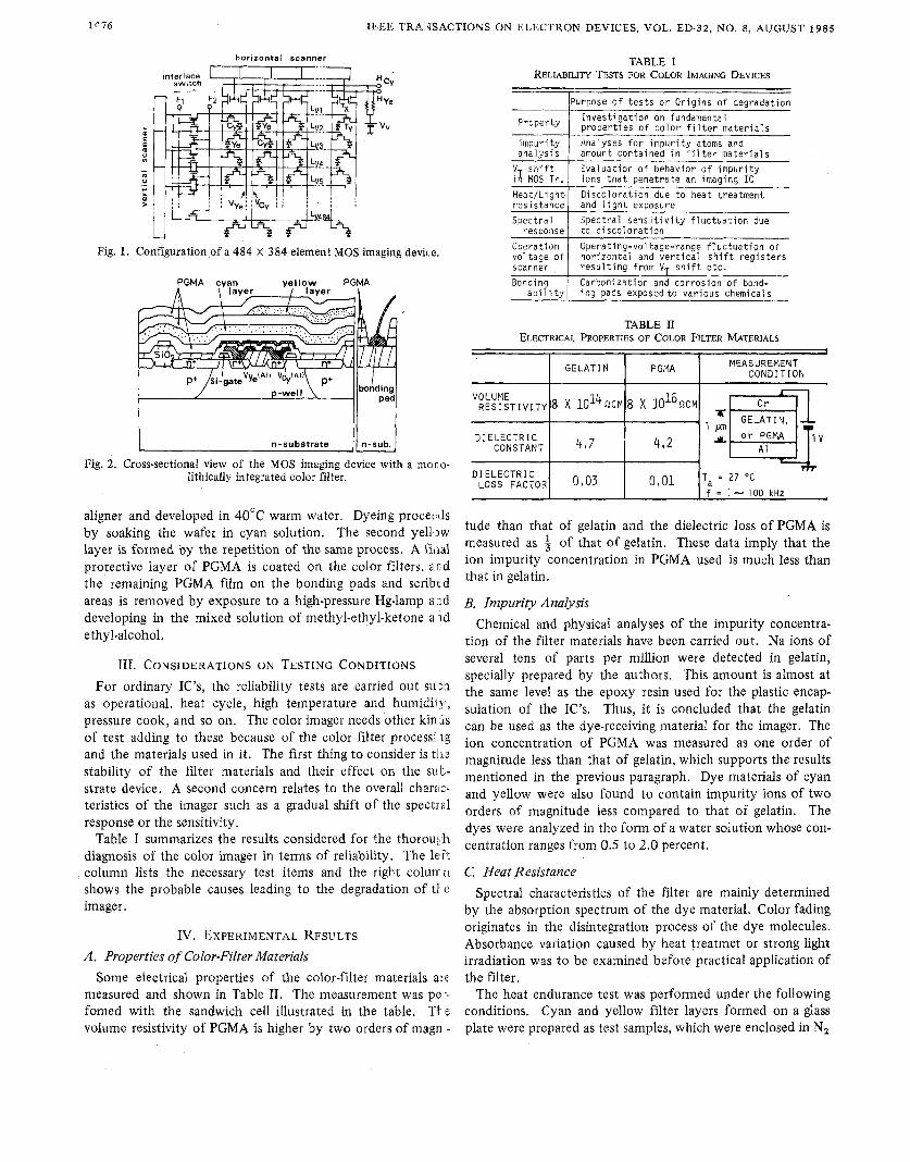
The MOS-type single-chip color imager normally employs mosaic complementary color filters consisting of cyan, yellow, green, and white [7]. Of these four color components, cyan and yellow are the two layers actually formed, while green is made of the superposition of these two and white represents a pixel without any color filters. As shown in Fig. 1, a test de- vice with cyan and yellow filters in ai checkerboard arrange- ment was prepared. The device has a sensitive area of 1-in format for the purpose of obtaining a signal with high S/N ratio to increase the measurement accuracy.
B. Device Structure A cross section of the device is shown in Fig. 2 . The color-
filter layers are deposited on the passivated surface of the im- ager. The overlapped region of cyan and yellow forms a green portion in the actual device. Three layers of poly glycidyl methacrylate (PGMA) are used for the protection of color- filter layers.
C. Device Fabrication For the fabrication of the integrated color filters, a method
which heat transfers sublimable dye to an organic dye-receiving material has been reported [ l ] , [2] . However, this method was found in our experiments to have problems such as repro- ducibility of spectral reponse and cross-color dyeing. The authors have overcome these problems by refining the conven- tional wet process utilizing water-soluble dyes.
In this process, gelatin was chosen a.s a receiving material be- cause of its high heat-resistance characteristics over 200°C compared to other materials like poly-vinyl-alcohol. PGMA intermediate layers were also chosen for superior heat and chemical resistance properties.
In order to flatten the uneven imager surface, the PGMA film is spin-coated, and the first gelatin layer is formed over it. Next, the gelatin layer is exposed by using 10 to 1 reduction
0018-9383/85/0800-1475$01.00 0 1985 IEEE
IEEE TRA rlSACTIONS ON ELECTRON DEVICES, VOL. ED-32, NO. 8, AUGUST 1985
horizontal scannel
Fig. 1. Configuration of a 484 X 384 element MOS imaging devic,e.
PGMA c an e l low PGMA
n - s u b s t r a t e I ( n-sub. 1 Fig. 2. Cross-sectional view of the MOS imaging device with a mono-
lithically integrated color filter.
aligner and developed in 40°C warm water. Dyeing proceds by soaking the wafer in cyan solution. The second yellow layer is formed by the repetition of the same process. A A1131
protective layer of PGMA is coated on the color filters, and the remaining PGMA film on the bonding pads and scritlcd areas is removed by exposure to a high-pressure Hg-lamp a ~ d developing in the mixed solution of methyl-ethyl-ketone a Id ethyl-alcohol.
111. CONSIDERATIONS ON TESTING CONDITIONS For ordinary IC’s, the reliability tests are carried out su :n
as operational, heat cycle, high temperature and humidi.ly, pressure cook, and so on. The color imager needs other kin 3.s of test adding to these because of the color filter processi IB
and the materials used in it. The first thing to consider is t l ~ stability of the filter materials and their effect on the s u b strate device. A second concern relates to the overall charac- teristics of the imager such as a gradual shift of the spectral response or the sensitivity.
Table I summarizes the results considered for the thoroui1-1 diagnosis of the color imager in terms of reliability. The left column lists the necessary test items and the right co1un;n shows the probable causes leading to the degradation of tE t:
imager.
IV. EXPERIMENTAL RESULTS A . Properties of Color-Filter Materials
Some electrical properties of the color-filter materials a::e measured and shown in Table 11. The measurement was pe ... fomed with the sandwich cell illustrated in the table. The volume resistivity of PGMA is higher by two orders of magn .
TABLE I RELIABILITY TESTS FOR COLOR IMAGING DEVICES
l P u r p o s e o f t e s t s o r O r i q i n s o f d e a r a d a t i o n
Property 1 Inves t iga t ion on fundamenta l p r o p e r t i e s o f c o l o r f i l t e r m a t e r i a l s
a n a l y s i s i m p u r i t y
amount c o n t a i n e d i n f i l t e r m a t e r i a l s Ana lyses fo r impur i ty a toms and
V s h i f t
D i s c o l o r a t i o n due t o h e a t t r e a t m e n t H e a t / L i a h t
i o n s t h a t p e n e t r a t e a n i m a g i n g IC iA MOS Tr. E v a l u a t i o n o f b e h a v i o r o f i m p u r i t y
r e s i s t a n c e
t o d i s c o l o r a t i o n resuonse S p e c t r a l s e n s i t i v i t y f l u c t u a t i o n due Spec t ra l
and l i g h t e x p o s u r e
TABLE I1 ELECTRICAL PROPERTIES OF COLOR FILTER MATERIALS
J
GELAT 1 N PGMA MEASUREMENT CONDITION
VOLUME R E S I S T I VITY 8 X 1 O l 6 , c ~ 8 X
DIELECTRIC CONSTANT 4 1 4 , 2
DIELECTRIC LOSS FACTOR 0 ,01 0103 Ta = 27 O C
f = 1 - 100 kHz
tude than that of gelatin and the dielectric loss of PGMA is measured as f of that of gelatin. These data imply that the ion impurity concentration in PGMA used is much less than that in gelatin.
B. Impurity Analysis Chemical and physical analyses of the impurity concentra-
tion of the filter materials have been carried out. Na ions of several tens of parts per million were detected in gelatin, specially prepared by the authors. This amount is almost at the same level as the epoxy resin used for the plastic encap- sulation of the IC’s. Thus, it is concluded that the gelatin can be used as the dye-receiving material for the imager. The ion concentration of PGMA was measured as one order of magnitude less than that of gelatin, which supports the results mentioned in the previous paragraph. Dye materials of cyan and yellow were also found to contain impurity ions of two orders of magnitude less compared to that of gelatin. The dyes were analyzed in the form of a water solution whose con- centration ranges from 0.5 to 2.0 percent.
C. Heat Resistance Spectral characteristics of the filter are mainly determined
by the absorption spectrum of the dye material. Color fading originates in the disintegration process of the dye molecules. Absorbance variation caused by heat treatmet or strong light irradiation was to be examined before practical application of the filter.
The heat endurance test was performed under the following conditions. Cyan and yellow filter layers formed on a glass plate were prepared as test samples, which were enclosed in N2

KOIKE er al.: CHARACTERISTICS OF AN MOS IMAGING DEVICE 1477
TEMPERATURE : I / T X ~ O ~ ( ~ K - ' )
Fig. 3. Heat-resistance characteristics of cyan and yellow filters.
gas-filled ampoule and heated for a certain period of time. The absorbance was measured before and after heat treatment. The results are shown in Fig. 3. The absorbance fluctuation time 'on the left vertical axis is defined as the time taken to generate a 10-percent fluctuation. The IO-percent absorbance fluctua- tion corresponds to the variation from 6 to 8 percent in trans- mittance at the absorption region. This variation level can usu- ally be assumed to be of no problem for most TV camera applications.
The color fading can be considered to progress in the first- order thermal-decomposition reaction. Then, the absorbance K after heat-treatment for a period of t can be expressed by the exponential formula
K =KO exp (- f) where K O is the absorbance before heat-treatment. The time constant 7, defined by (l), is represented by the right-side vertical axis in Fig. 3.
From the data plotted in the figure, the following experi- mental formulas can be derived:
9.4 x 10³ T
log t = - 18.6 for yellow filter
1.0 x 10⁴ log t =
T - 18.9 for cyan filter
where T is the treating temperature (in Kelvins). The heat resistance of the yellow filter is a little weaker than that of the cyan filter.
The life time, defined by the absorbance fluctuation time, can be calculated by using (2); 9.9 X lo4 h (-1 1 years) for yellow and 1.6 X lo6 h (-180 years) for cyan under the am- bient temperature of 125°C.
D. Light Resistance Fig. 4 shows the results of the measurement on the light
resistance of the filters. The test samples are also enclosed in a N2 gas-filled glass container and exposed to the light. The data with "1 indicate that the samples were placed by the window side of the laboratory room during the daytime to be exposed to sun light of about 1500-1x illumination on average. The "2 data indicate the samples were held under the light source of 3200°K color temperature. The results obtained
lo-' 103 lo4 15 106 lo7
LIGHT INTENSITY (I>[)
Fig. 4. Light-resistance characteristics of cyan and yellow filters.
TABLE I11 HALF-VALUE WAVELENGTH FLUCTUATION CHARACTERISTICS OF CYAN AND
YELLOW FILTERS
I N I T I A L AMOUNT ( t = 8750 HOURS) ( t = 0 HOUR)
S H I F T AFTER ONE YEAR
I
F;;ItzR - 1 nm 494 nm
0 n m 563 n m 563 nm
,YELLOW 495 nm F I LTER
(The filter samples have been exposed to light intensity of 1500 l x for 1 year.)
lead to the following experimental relations:
t X @ = 106n8 for yellow filter
t X @ = 106.9 for cyan filter (3)
where t$ is the incident light intensity in lux. The life time t is inversely proportional to the light intensity. The estimated life time is about 13 years for yellow and 18 years for cyan under the illumination of 50 lx.
Table 111 shows the variation in half-value-wavelength of the filter, measured under exposure to sun light of about 1500-1x illumination. Almost negligible shift was observed.
E. Threshold Voltage Shift Three kinds of test MOS transistors were fabricated: 1) gela-
tin-film coated, 2 ) gelatin film containing green dye coated, and 3) without coating. As shown in Fig. 5(c), the test tran- sistor has a hole, coated with gelatin, in the vicinity of its gate region, and this hole can be considered as a contamination source.
A dynamic test under operational condition at 125°C and a storage test at 150°C were performed, and the results of the threshold voltage measurement for both active and parasitic MOS transistors are shown in Fig. 5(a) and (b). Each datum represents the averaged value for the same 10 test samples. The observed threshold voltage shift for the active transistor is about 5 mV over a period of 1000 h and corresponds to only & of the original threshold of 0.45 V. The shift for the parasitic transistor is about 100 mV, & of the original threshold of 8.4 V.
The preceding results lead to the conclusion that the ob-

IEEE TRAI'?IACTIONS ON ELECTRON DEVICES, VOL. ED-32, NO. 8, AUGUST 1985
TESTING TiME : t (Hour)
@)
contamination I source
A , contamination e
L p-sub. p-sub.
(c) Fig. 5. Threshold-voltage shift. (a) Active MOS transistors. (b) Para-
sitic MOS transistors. (c) Structure of test device.
served shift in the threshold voltage will little affect dey,ice operation or can be easily treated within the margin of h e device design, and that the gelatin material can coexist with the silicon substrate.
F. Spectral Response Variation The imagers with cyan and yellow filters, mentioned, in
Section I, were tested for a period of 1000 h under conditi1:ms of 125°C operation and 150°C storage. The results are sho m in Fig. 6 . The figures indicate that the variation in spec;lral response is within 5 percent and will not cause any practi :a1 problems for the stability of color reproduction.
G. Shift Register Operation The horizontal and vertical shift registers consist of bootstrilp-
type noninverting circuits and ratio-type inverting circuits, x- spectively [8], The lowest voltage necessary for their opa:a- tion was measured and is plotted in Fig. 7. The variation of the voltage over 1000 h is observed as around 150 mV for tile horizontal and 60 mV for the vertical register. This amotlx?t of variation remains well within the normal operational marj,in of 9 V f 10 percent.
H. Bonding Ability The A1 bonding pads of the imager contacts are covered wlt.l?
filter materials and other chemicals during color-filter proces- ing and this might cause problems in wire bonding. Bond- ability strength tests were carried out for the imagers wi:j!~ and without color filters. The results are shown in Fig. 5. Bondability, here, is defined as the strain strength which j u s t breaks the A1 bonding wire by way of hooking. Fig. 8(a) a1.d
-. 0' =I I ' ' ? - ' ' ' 400 503 600 700 800
WAVELENGTH (nrn)
(b) Fig. 6. Spectral-response variation. @ and @ show the Position of
the half-value wavelength for the yellow and the cyan filter, respeo tively. (a) Storage test at 150°C. (b) Operating test a t 125°C.
horizontal scanner
9
1 opemtion.1a'c:
..*.. )mn-operatW.1W'c:
10 100 loo0
..*--
TESTING TIME : t (Hour)
Fig. 7. Variation of the operational voltage for the registers.
STRAIN STRENGTH ( 9 ) fa)
STRAIN STRENGTH (9 1 co)
Fig. 8. Strain-strength test for evaluating bonding ability. (a) Imager with color filter. (b) Imager without color filter.
(b) shows almost the same distribution for the device with and without color filters and it can be concluded that color-filter processing does not cause degradation in bondability.
I. Others Adding to these tests, variation in saturation current and
blemish generation were also evaluated. Almost no discernible

ROIKE etal.: CHARACTERISTICS OF AN MOS IMAGING DEVICE 1479
change was observed over a period of 1000 h in operation and storage.
V. CONCLUSION Before the practical application of the on-wafer color-filter
processing utilizing gelatin receiving material, dyes, and PGMA protecting films, various reliability tests were performed. All the results described in this paper indicate that color-filter processing can coexist with normal LSI processing and the im- ager with color filters can be considered to have the same’level of reliability with other 1231’s. Moreover, a ceramic package with a hermetically sealed optical glass window has been de- veloped for the imager, and this also assures a long stable op- erational life.
The commercial imager, fabricated by on-wafer color-filter processing, has been on the market for more than three years and, to the author’s knowledge, no reliability problems have been reported.
ACKNOWLEDGMENT The authors wish to thank J. Koike for his help in device
fabrication, and Dr. M. Hashimoto and K. Chiba for their tech- nical support. Thanks are also due to Dr. M. Kubo, Dr. M. Ashikawa, S . Ohba, M. Aoki, A. Izumi, and S. Koishikawa for their continuous encouragement and useful discussions.
REFERENCES [ 11 P. L. P. Dillon, A. Brualt, J. R. Horak, E. Garcia, T. Martin, and
W. A. Light, “Fabrication and performance of color filter arrays for solid-state imagers,” IEEE Trans. Electron Devices, vol. ED-25, pp. 97-101, Feb. 1978.
[2] W. C. McColgin, T. W. Martin, A. K. Weiss, and M. A. Sandhu, “Integral color filter arrays for solid-state imagers by thermal transfer of dyes,” IEEE Trans. Electron Devices, vol. ED-26, p. 1855, Nov. 1979.
[3] T. Nakano, Y . Taniguchi, T. Kaneko, IC, Tsutsui, M. Hashimoto, y. Koike, A. Izumi, and A. Sasano, “On-wafer color filter for solid-state imagers,” in Nut. Conv. Rec. Inst. Telev. Eng. Japan,
[4] A. Sasano, T. Nakano, Y. Taniguchi, M. Hashimoto, N. Koike, A. Izumi, T. Horiuchi, and T. Fujita, “Monolithically fabricated color filter arrays for single chip solid-state imagers,” J. Inst. Telev. Eng. Japan, vol. 37, pp. 553-558, July 1983.
[SI T. Nakano, A. Sasano, M. Hgshimoto, T. Kaneko, H. Matsumaru, J. Takemoto, and E. Maruyama, “Color filter for solid-state im- agers,” in Nat. Conv. Rec. Inst. Telev. Eng. Japan, pp. 63-64, 1979.
[6 ] N. Koike, T. Nakano, A. Sasano, I. Takemoto, Y. Taniguichi, A. Izumi, and T. Fujita, “Reliability-charac.teristic analyses and mea- surements of a single-chip color MOS imaging device,” in Nut. Conv. Rec. Inst. Telev. Eng. Japan, pp. 25-26, 1982.
[7] M. Aoki, H. Ando, S. Ohba, I. Takemoto, S. Nagahara, T. Nakano, and M. Kuko, “2/3-in format MOS sing1e)chip color imager,” IEEE Trans. Electron Devices, vol. ED-29, pp. 745-’750, Apr. 1982.
[8] N. Koike, I. Takemoto, K. Satoh, S. Hanamura, S. Nagahara, and M. Kubo, “MOS area sensor: Part 1-Desjgn consideration and per- formance of an n-p-n structure 484 X 384 element color MOS imager,” IEEE Trans. Electron Devices, vol. ED-27, pp. 1676- 1681, Aug. 1980.
pp. 21-22,1980.