hartcran house, 231 kenton lane, harrow, … ltd., tx1 & rx1 data sheet page 2 functional...
TRANSCRIPT

Radiometrix Ltd., TX1 & RX1 Data Sheet page 1
Features
CE Certified by independent Notified Body Verified to comply with harmonised EU standards ETSI EN 300 220-3 (radio) and EN 301 489-3
(EMC) by accredited Test Laboratory Frequencies available as standard: 173.225MHz, 173.250MHz Other frequencies from 151.300MHz to 173.250MHz available to order Data rates up to 10 kbps with 25kHz channel spacing Usable range to 10km+ Screened construction
Available for licence-exempt operation in the UK 173MHz bands, the TX1 & RX1 modules combine effective screening with internal filtering to minimise spurious radiation and susceptibility thereby ensuring EMC compliance. They are particularly suitable for one-to-one and multi-node wireless links where longer ranges are required at low to moderate data rates. Applications include building security, EPOS and inventory tracking, remote industrial process monitoring and data networks. Because of their small size and low power consumption, both modules are ideal for use in battery-powered portable applications such as hand-held terminals.
Technical Summary Transmitter - TX1
2 stage crystal controlled, NBFM modulated at up to 10 kb/s Operation from 2.2V to 12V @ 9.5mA Built-in regulator for improved stability and supply noise rejection
Exceptional power efficiency, typically 35% DC → RF @ 3V supply +10dBm (10mW) RF output Harmonics typically -70dBc Enable facility
Receiver - RX1 Single conversion NBFM superhet Image rejection >50dB Operation from 2.7V to 12V @ 12mA Built-in regulator for improved stability and supply noise rejection 10kbps, -116dBm sensitivity @ 1ppm BER RSSI output with >80dB range Local oscillator leakage <-60 dBm Enable facility
Evaluation platforms: NBEK + SIL carrier
left: TX1 transmitter right:RX1receiver
The TX1 and RX1 form a miniature VHF radio transmitter/receiver pair designed for PCB mounting and suitable for extended range data links at speeds up to 10kbps. Link ranges of 10km+ are achievable with suitable choice of data rate and antennas.
VHF Narrow Band FM Transmitter and Receiver VHF Narrow Band FM Transmitter and Receiver VHF Narrow Band FM Transmitter and Receiver VHF Narrow Band FM Transmitter and Receiver
Hartcran House, 231 Kenton Lane, Harrow, Middlesex, HA3 8RP, England Tel: +44 (0) 20 8909 9595, Fax: +44 (0) 20 8909 2233, www.radiometrix.com
Issue 2, 01 August 2012 TX1 / RX1

Radiometrix Ltd., TX1 & RX1 Data Sheet page 2
Functional description The TX1 module is a two stage crystal controlled NBFM transmitter operating between 2.2V and 12V at a current of 9.5mA. At 3V supply it delivers nominally +10dBm RF output. The SIL style TX1 measures 32 x 12 x 3.8 mm excluding the pins. The RX1 module is a single conversion NBFM superhet receiver capable of handling data rates of up to 10kbps. It will operate from a supply of 2.7V to 12V and draws 12mA when receiving. A signal strength (RSSI) output with greater than 80dB of range is provided. The SIL style RX1 measures 48 x 17.5 x 5.5 mm excluding the pins.
TX1 transmitter
Lowpass filter
PA
Bandpass filter
x2
VCXO
7kHz LPF
100k
Supply
regulator
1RF gnd
2RF out
3RF gnd
4En
5Vcc
60V
7TXD
En (pin 4)
Tx enable. ≤0.15V on this pin disables module (current <1µA), ≥1.7V enables module. Input impedance 1MΩ approx. Observe slew rate requirements (see applications notes). Vcc (pin 5) DC +ve supply. Max ripple content 0.1VP-P. Decoupling is not generally required. 0V (pin 6) DC supply ground. Internally connected to pins 1, 3 and module screen. TXD (pin 7) DC-coupled modulation input. Accepts serial digital data at 0V to 3V levels.
See applications notes for suggested drive methods. Input impedance 100kΩ nominal.
Fig.2: TX1 physical dimensions
Pin description RF gnd (pins 1 & 3) RF ground, internally connected to the module screen and pin 6 (0V). These pins should be directly connected to the RF return path - e.g. coax braid, main PCB ground plane etc. RF out (pin 2)
50Ω RF output to antenna. Internally DC-isolated. See antenna section of applications notes for details of suitable antennas / feeds.
Fig.1: TX1 block diagram
3.8 mm32 mm
12.0
mm
12.5
mm
PCB level
Radiometrix
TX1pin spacing: 2.54 mm
7 holes of 0.7 mm dia. pin spacing 2.54 mm
15.24 mm
1 2 3 4 5 6 7
1 = RF gnd
2 = RF out3 = RF gnd4 = En
6 = 0V7 = TXD
5 = Vcc

Radiometrix Ltd., TX1 & RX1 Data Sheet page 3
RX1 receiver
Bandpass filter
x2
7kHz LPF
Supply
regulator
3RF gnd
1RF in
2RF gnd
4En
7Vcc
60V
Preamp.
Mixer
Bandpass filterXtal osc/mult.
IF1 IF2
IF amplification / filteringFM
discriminator
Regulated
Rx supply
5RSSI
9RXD
8AF out
AF buffer
Adaptive
data slicer
10k
En (pin 4)
Rx enable. ≤0.15V on this pin disables module (current <1µA), ≥1.7V enables module. Input impedance 1MΩ approx. Observe slew rate requirements (see applications notes). RSSI (pin 5) Received Signal Strength Indicator with >80dB range. See applications notes for typical characteristics. 0V (pin 6) DC supply ground. Internally connected to pins 2, 3 and module screen. Vcc (pin 7) DC +ve supply. Max ripple content 0.1VP-P. Decoupling is not generally required. AF out (pin 8) Buffered and filtered analogue output from the FM demodulator. It has a standing DC bias of 1V and 400mVP-
P baseband signal. Useful as a test point or to drive external decoders (see applications notes). External load
should be >1kΩ // <100pF. RXD (pin 9) Digital output from internal data slicer (squared version of the signal on pin 8). It may be used to drive external decoders. The data is true data, i.e. as fed to the transmitter. Output is “open-collector” format with
internal 10kΩ pullup to Vcc (pin 7).
Pin description RF in (pin 1)
50Ω RF input from antenna. Internally DC-isolated. See antenna section of applications notes for suggested antennas and feeds. RF gnd (pins 2 & 3) RF ground, internally connected to the module screen and pin 6 (0V). These pins should be directly connected to the RF return path - e.g. coax braid, main PCB ground plane etc.
Fig.3: RX1 block diagram
Fig.4: RX1 physical dimensions
9 holes of 0.7 mm dia. pin spacing 2.54mm
1 2 3
48 mm
17.5
mm 1
8.0
mm
PCB level
RadiometrixRX1
4 5 6 7 98
25.4 mm
pin spacing: 2.54 mm
1 = RF in2 = RF gnd3 = RF gnd4 = En5 = RSSI6 = 0V7 = Vcc8 = AF out9 = RXD
5.5 mm

Radiometrix Ltd., TX1 & RX1 Data Sheet page 4
Absolute maximum ratings Exceeding the values given below may cause permanent damage to the module.
Operating temperature -20°C to +60°C
Storage temperature -40°C to +100°C TX1 Vcc, TXD (pins 5,7) -0.3V to +16.0V En (pin 4) -0.3V to +Vcc V
RF out (pin 2) ±50V @ <10MHz, +20dBm @ >10MHz RX1 Vcc, RXD (pins 7,9) -0.3V to +16.0V En, RSSI, AF (pins 4,5,8) -0.3V to +Vcc V
RF in (pin 1) ±50V @ <10MHz, +13dBm @ >10MHz
Performance specifications: TX1 transmitter (Vcc = 3.0V / temperature = 20°C unless stated)
pin min. typ. max. units notes DC supply Supply voltage 5 2.2 3.0 12 V Supply current 5 9.5 11 mA RF RF power output @ Vcc = 2.2V 2 +4.5 +6 +7.5 dBm 1
RF power output @ Vcc ≥ 2.8V 2 +8.5 +10 +11.5 dBm 1
Spurious emissions 2 -70 -55 dBc 2 Frequency accuracy -2.0 0 +2.0 kHz 3 FM deviation (peak) ±2.5 ±3.0 ±3.5 kHz 4
Baseband Modulation bandwidth @ -3dB 0 7 kHz Modulation distortion (THD) 10 15 % 7 TXD input level (logic low) 7 -0.2 0 0.2 V 5,7 TXD input level (logic high) 7 2.8 3.0 3.2 V 5,7 Dynamic timing
Power-up time (En → full RF) 2 5 ms 6,7
Notes:
1. Measured into 50Ω resistive load. 2. Exceeds EN/EMC requirements at all frequencies. 3. Total over full supply and temperature range. 4. With 0V – 3.0V modulation input. 5. To achieve specified FM deviation. 6. Dependent upon TXD conditions during power-up. 7. See applications information for further details.

Radiometrix Ltd., TX1 & RX1 Data Sheet page 5
Performance specifications: RX1 receiver (Vcc = 3.0V / temperature = 20°C unless stated)
pin min. typ. max. units notes
DC supply Supply voltage 7 2.7 3.0 12 V Supply current 7 12 14 mA RF/IF RF sensitivity @ 10dB (S+N)/N 1, 8 -119 -115 dBm RF sensitivity @ 1ppm BER 1, 9 -116 -112 dBm IP3 at RF input 1 -28 dBm RSSI threshold 1, 5 -127 dBm 1 RSSI range 1, 5 80 90 dB 1 IF bandwidth 15 kHz Image rejection 1 50 55 dB Adjacent channel rejection 1 50 55/60 dB 2 Spurious response rejection 1 70 100 dB LO leakage, conducted 1 -70 -65 dBm 3 LO leakage, radiated -70 -60 dBm 3 Baseband Baseband bandwidth @ -3dB 8 0.05 6 kHz 1, 4 AF level 8 400 mVP-P 5 DC offset on AF out 8 0.7 1.0 1.3 V Distortion on recovered AF 8 1 10 % Load capacitance, AFout / RXD 8, 9 100 pF Dynamic timing Power up with signal present Power up to valid RSSI 4, 5 4 5 ms Power up to stable data 4, 9 16 20 ms Signal applied with supply on Signal to valid RSSI 1, 5 0.4 0.6 ms Signal to stable data 1, 9 4 12 ms 6 Time between data transitions 9 1.8 0.1 ms 7 Mark : space ratio 9 20 50 80 % 8
Notes: 1. See applications information for further details. 2. Typically 55dB @ +25kHz offset, 60dB @ -25kHz offset. 3. Exceeds EN/EMC requirements at all frequencies. 4. Lower limit can be extended to DC if required, by means of external circuitry.
5. For received signal with ±3kHz FM deviation.
6. Typically 4ms for signal at channel centre, maximum 12ms at ±4kHz RF offset. 7. For 50:50 mark to space ratio (i.e. squarewave). 8. Average over 50ms period at maximum bit rate.

Radiometrix Ltd., TX1 & RX1 Data Sheet page 6
Module test circuits
Radiometrix
TX1
TXD
Vcc
0V (GND)
1 2 3 4 5 76
En
50 ΩRF out
3V
0V
5kHz max.
Fig.5: TX1 test circuit
RadiometrixRX11 2 3 8 94 5 6 7
RF in50Ω
RXD
RSSI
AF out
Vcc
En
0V (GND)
Fig.6: RX1 test circuit
Applications information
Power supply requirements Both modules have built-in regulators which deliver a constant 2.85V to the module circuitry when the external supply voltage is 2.9V or greater, with 40dB or more of supply ripple rejection. This ensures constant performance up to the maximum permitted rail, and removes the need for external supply decoupling except in cases where the supply rail is extremely poor (ripple/noise content >0.1Vp-p). Note, however, that for supply voltages lower than 2.85V the regulator is effectively inoperative and supply ripple rejection is considerably reduced. Under these conditions the ripple/noise on the RX1 supply rail should
be below 20mVp-p to avoid problems. If the quality of the supply is in doubt, it is recommended that a 10µF
tantalum or similar capacitor be added between pin 7 of the module (Vcc) and ground together with a 10Ω series feed resistor between pin 7 and the supply rail. The Enable pin allows the module to be turned on or off under logic control with a constant DC supply to the
Vcc pin. The module current in power-down mode is less than 1µA.
NOTE: If this facility is used, the logic control signal must have a slew rate of 40mV/µs or more. Slew rates less than this value may cause erratic operation of the on-board regulator and therefore the module itself. The Enable pin should be tied directly to the Vcc pin if this facility is not required.

Radiometrix Ltd., TX1 & RX1 Data Sheet page 7
TX1 modulation requirements The module is factory-set to produce the specified FM deviation with a TXD input to pin 7 of 3V amplitude, i.e. 0V “low”, 3V “high”. Reducing the amplitude of the data input from this value (usually as a result of reducing
the supply voltage) reduces the transmitted FM deviation to typically ±2.5kHz at the lower extreme of 2.2V. The receiver will cope with this quite happily and no significant degradation of link performance should be observed as a result. Where the module supply is greater than 3V a resistor must be added in series with the TXD input to limit the
modulation amplitude to a maximum of 3V on pin 7. TXD input resistance is 100kΩ to ground, giving typical required resistor values as follows:
Vcc Series resistor
≤3V 3.3V 5V 9V
-
10 kΩ
68kΩ
220kΩ
It should be noted that conditions on TXD have a significant effect on the startup time of the module, i.e. the time between En (or En+Vcc) going high and full RF output being produced. For fastest startup TXD should either be low or fed with data (preamble etc) for a minimum of 3ms after En has been asserted. Startup time under these conditions is typically 50-70% of that obtained if TXD is held high over the same period.
Reducing the output power of the TX1 If the TX1-173.250-10 is to be used for other than industrial/commercial applications its output power must be reduced to 1mW to comply with type approval requirements. This is done by inserting a 10dB attenuator network between the module and the antenna or feed, as follows:
TX1
1 2 3 4 5 76
68R
100R
antenna
10
0R
10
0R
68R
ground foil/vias to ground plane
50 ohm microstrip lines
to antenna from TX1
schematic diagram physical arrangement
Resistors are SMD (0603/0805)
Fig.7: 10dB attenuator for TX1 Keep all tracking around the attenuator network as short as possible, particularly ground paths, and use
matched 50Ω microstrip lines for input and output connections (track width of 2.5mm if using 1.6mm thick FR4 PCB).

Radiometrix Ltd., TX1 & RX1 Data Sheet page 8
RX1 Received Signal Strength Indicator (RSSI) The RX1 receiver incorporates a wide range RSSI which measures the strength of an incoming signal over a range of 80dB or more. This allows assessment of link quality and available margin and is useful when performing range tests. Please note that the actual RSSI voltage at any given RF input level varies somewhat between units. The RSSI facility is intended as a relative indicator only - it is not designed to be, or suitable as, an accurate and repeatable measure of absolute signal level or transmitter-receiver distance. The output on pin 5 of the module has a standing DC bias of 0.15V-0.45V (0.25V typ.) with no signal, rising to
0.9-1.3V (1.15V typ.) at maximum indication. Output impedance is 10kΩ. Pin 5 can drive a 100A meter directly, for simple monitoring. Typical RSSI characteristic is shown below (this is for indicative purposes only and is not a guarantee of actual RSSI characteristics):
0
0.2
0.4
0.6
0.8
1
1.2
-125
-120
-115
-110
-105
-100 -9
5-9
0-8
5-8
0-7
5-7
0-6
5-6
0-5
5-5
0-4
5-4
0-3
5
RF Input Level (dBm)
RS
SI O
utp
ut V
oltage (
V)
Fig.8: Typical RSSI response curve To ensure a reasonably fast response the RSSI line has limited internal decoupling of 11nF to ground. This results in a small amount of audio ripple on the DC output at pin 5 of the module. If this is a problem further decoupling may be added at the expense of response speed, in the form of a capacitor from pin 5 to ground. For example, adding an extra 0.1F on this pin will increase the RSSI response time to around 4ms.
Expected range Predicting the range obtainable in any given situation is notoriously difficult since there are many factors involved. The main ones to consider are as follows:
• Type and location of antennas in use (see pages 10-12)
• Type of terrain and degree of obstruction of the link path
• Sources of interference affecting the receiver
• “Dead” spots caused by signal reflections from nearby conductive objects
• Data rate and degree of filtering employed (see page 9)
The following are typical examples – but range tests should always be performed before assuming that a particular range can be achieved in a given situation:
Data rate Tx antenna Rx antenna Environment Range 1.2kbps half-wave half-wave rural/open 10-15km 10kbps half-wave half-wave rural/open 3-4km 10kbps helical half-wave urban/obstructed 500m-1km 10kbps helical helical in-building 100-200m
Note: The figure for 1.2kbps assumes that the receiver bandwidth has been suitably reduced by utilising an
outboard audio filter/data slicer or similar arrangement. If the RX1 is used “as is” the range will be similar to that for 10kb/s.

Radiometrix Ltd., TX1 & RX1 Data Sheet page 9
Data formats and range extension The TX1 data input is normally driven directly by logic levels but will also accept analogue drive (e.g. 2-tone signalling). In this case it is recommended that TXD (pin 7) be DC-biased to 1.2V approx. with the modulation ac-coupled and limited to a maximum of 2Vp-p to minimise distortion over the link. The varactor modulator in the TX1 introduces some 2
nd harmonic distortion which may be reduced if necessary by predistortion of the
analogue waveform. At the other end of the link the RX1 AF output is used to drive an external decoder directly. Although the modulation bandwidth of the TX1 extends down to DC, as does the AF output of the RX1, it is not advisable to use data containing a DC component. This is because frequency errors and drifts between the transmitter and receiver occur in normal operation, resulting in DC offset errors on the RX1 audio output. The RX1 in standard form incorporates a low pass filter with a 6kHz nominal bandwidth. In conjunction with similar filtering in the TX1 an overall system bandwidth of 5kHz is obtained. This is suitable for transmission of data at raw bit rates up to 10kb/s. A lower rolloff frequency of around 50Hz has been chosen for the internal filter and data slicer in order to keep receiver settling times reasonably fast. This results in a lowest usable data speed of about 1kb/s for the standard module. In applications such as long range fixed links where data speed is not of prime concern, a considerable increase in range can be obtained by using the slowest possible data rate together with filtering to reduce the receiver bandwidth to the minimum necessary. The internal data slicer is not suitable for data having longer than 1.8ms between transitions and in such circumstances the RX1 audio output can be utilised to drive an external filter and data slicer. The RX1 produces an audio output of approximately 400mVp-p at pin 8, but due to the internal filtering this exhibits a rolloff at low frequencies giving a reduced output of some 100mVp-p as DC is approached. This rolloff can be eliminated and a flat response to DC obtained by using an external RC compensation network, as follows:
100k
33k
100nF
Input from
RX1 pin 8Output to low pass filter, etc.
100mV p-p, high impedance
Fig.9: Audio compensation network The output of the network will be flat from DC to 5kHz+. It will have a standing DC bias of 1V approx. and
should not be significantly loaded (input impedance of following stage should ideally be ≥1MΩ).

Radiometrix Ltd., TX1 & RX1 Data Sheet page 10
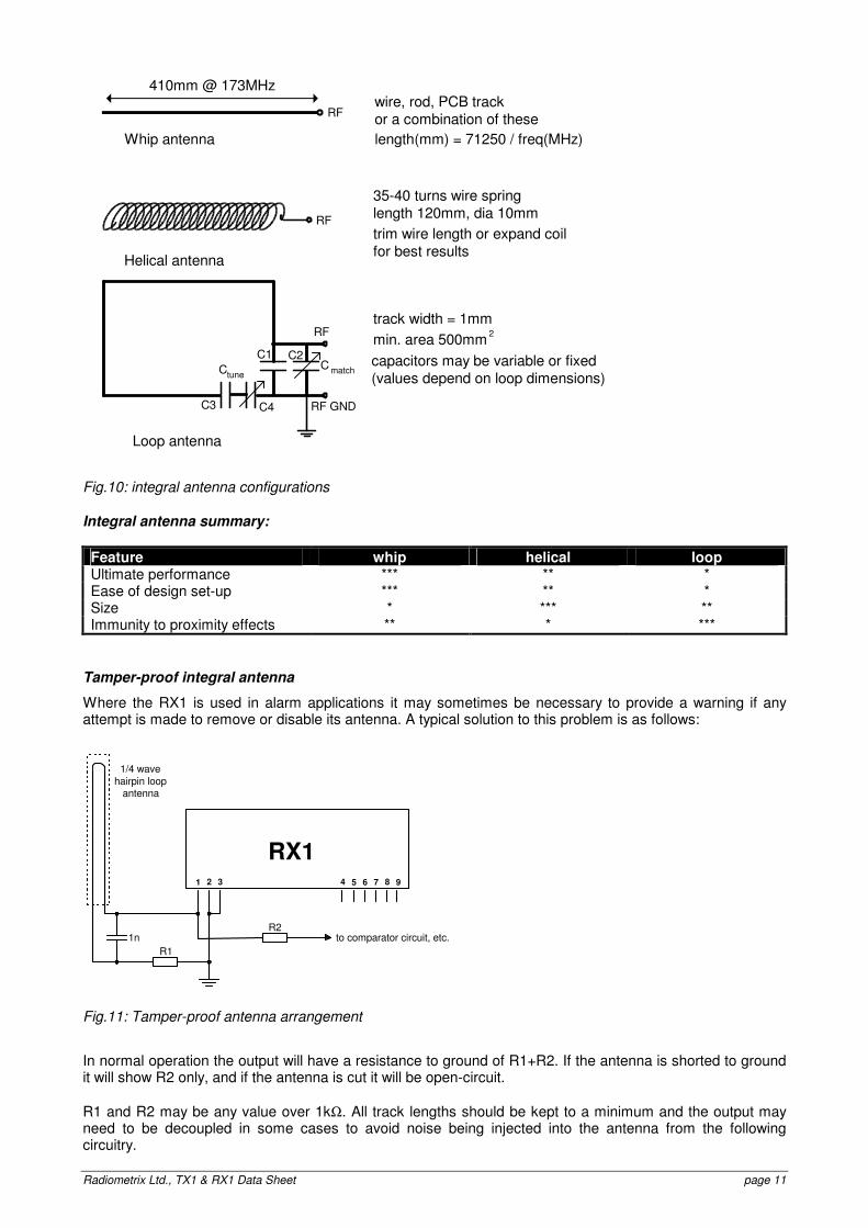
Antennas The choice and positioning of transmitter and receiver antennas is of the utmost importance and is the single most significant factor in determining system range. The following notes are intended to assist the user in choosing the most effective antenna type for any given application. Integral antennas These are relatively inefficient compared to the larger externally-mounted types and hence tend to be effective only over limited ranges. They do however result in physically compact equipment and for this reason are often preferred for portable applications. Particular care is required with this type of antenna to achieve optimum results and the following should be taken into account: 1. Nearby conducting objects such as a PCB or battery can cause detuning or screening of the antenna
which severely reduces efficiency. Ideally the antenna should stick out from the top of the product and be entirely in the clear, however this is often not desirable for practical/ergonomic reasons and a compromise may need to be reached. If an internal antenna must be used try to keep it away from other metal components and pay particular attention to the “hot” end (i.e. the far end) as this is generally the most susceptible to detuning. The space around the antenna is as important as the antenna itself.
2. Microprocessors and microcontrollers tend to radiate significant amounts of radio frequency hash which
can cause desensitisation of the receiver if its antenna is in close proximity. The problem becomes worse as logic speeds increase, because fast logic edges generate harmonics across the VHF range which are then radiated effectively by the PCB tracking. In extreme cases system range may be reduced by a factor of 5 or more. To minimise any adverse effects situate antenna and module as far as possible from any such circuitry and keep PCB track lengths to the minimum possible. A ground plane can be highly effective in cutting radiated interference and its use is strongly recommended.
A simple test for interference is to monitor the receiver RSSI output voltage, which should be the same regardless of whether the microcontroller or other logic circuitry is running or in reset. The following types of integral antenna are in common use: Quarter-wave whip. This consists simply of a piece of wire or rod connected to the module at one end. At 173MHz the total length should be 410mm from module pin to antenna tip including any interconnecting wire or tracking. Because of the length of this antenna it is almost always external to the product casing. Helical. This is a more compact but slightly less effective antenna formed from a coil of wire. It is very efficient for its size, but because of its high Q it suffers badly from detuning caused by proximity to nearby conductive objects and needs to be carefully trimmed for best performance in a given situation. The size shown is about the maximum commonly used at 173MHz and appropriate scaling of length, diameter and number of turns can make individual designs much smaller. Loop. A loop of PCB track having an inside area as large as possible (minimum about 5cm
2), tuned and
matched with 2 capacitors. Loops are relatively inefficient but have good immunity to proximity detuning, so may be preferred in shorter range applications where high component packing density is necessary.
Radiometrix Ltd., TX1 & RX1 Data Sheet page 11
Helical antenna
RF
Loop antenna
RF GND
RF
Ctune
Cmatch
capacitors may be variable or fixed
(values depend on loop dimensions)
track width = 1mm
min. area 500mm2
Whip antenna
410mm @ 173MHz
RFwire, rod, PCB track
or a combination of these
length(mm) = 71250 / freq(MHz)
trim wire length or expand coil
for best results
35-40 turns wire spring
length 120mm, dia 10mm
C1 C2
C3 C4
Fig.10: integral antenna configurations
Integral antenna summary:
Feature whip helical loop Ultimate performance *** ** * Ease of design set-up *** ** * Size * *** ** Immunity to proximity effects ** * ***
Tamper-proof integral antenna
Where the RX1 is used in alarm applications it may sometimes be necessary to provide a warning if any attempt is made to remove or disable its antenna. A typical solution to this problem is as follows:
Fig.11: Tamper-proof antenna arrangement
In normal operation the output will have a resistance to ground of R1+R2. If the antenna is shorted to ground it will show R2 only, and if the antenna is cut it will be open-circuit.
R1 and R2 may be any value over 1kΩ. All track lengths should be kept to a minimum and the output may need to be decoupled in some cases to avoid noise being injected into the antenna from the following circuitry.
RX11 2 3 8 94 5 6 7
R2
1/4 wave
hairpin loopantenna
R1
1n to comparator circuit, etc.

Radiometrix Ltd., TX1 & RX1 Data Sheet page 12
External antennas These have several advantages if portability is not an issue, and are essential for long range links. External antennas can be optimised for individual circumstances and may be mounted in relatively good RF locations away from sources of interference, being connected to the equipment by coax feeder. Helical. Of similar dimensions and performance to the integral type mentioned above, commercially-available helical antennas normally have the coil element protected by a plastic moulding or sleeve and incorporate a coax connector at one end (usually a straight or right-angle BNC type). These are compact and simple to use as they come pre-tuned for a given application, but are relatively inefficient and are best suited to shorter ranges. Quarter-wave whip. Again similar to the integral type, the element usually consists of a stainless steel rod or a wire contained within a semi-flexible moulded plastic jacket. Various mounting options are available, from a simple BNC connector to wall brackets, through-panel fixings and magnetic mounts for temporary attachment to steel surfaces. A significant improvement in performance is obtainable if the whip is used in conjunction with a metal ground plane. For best results this should extend all round the base of the whip out to a radius of 300mm or more (under these conditions performance approaches that of a half-wave dipole) but even relatively small metal areas will produce a worthwhile improvement over the whip alone. The ground plane should be electrically connected to the coax outer at the base of the whip. Magnetic mounts are slightly different in that they rely on capacitance between the mount and the metal surface to achieve the same result. A ground plane can also be simulated by using 3 or 4 quarter-wave radials equally spaced around the base of
the whip, connected at their inner ends to the outer of the coax feed. A better match to a 50Ω coax feed can
be achieved if the elements are angled downwards at approximately 30-40° to the horizontal.
Fig.12: Quarter wave antenna / ground plane configurations
50 Ω coax feed
Metal ground plane
50 Ω coax feed
30-40deg.
(3-4
, equ
ally spa
ced)
1/4-
wav
e ra
dial e
lem
ents
1/4-wave whip
(410m
m long @
173M
Hz)
1/4-wave whip

Radiometrix Ltd., TX1 & RX1 Data Sheet page 13
Half-wave. There are two main variants of this antenna, both of which are very effective and are recommended where long range and all-round coverage are required: 1. The half-wave dipole consists of two quarter-wave whips mounted in line vertically and fed in the centre
with coaxial cable. The bottom whip takes the place of the ground plane described previously. A variant is available using a helical instead of a whip for the lower element, giving similar performance with reduced overall length. This antenna is suitable for mounting on walls etc. but for best results should be kept well clear of surrounding conductive objects and structures (ideally >1m separation).
2. The end-fed half wave is the same length as the dipole but consists of a single rod or whip fed at the
bottom via a matching network. Mounting options are similar to those for the quarter-wave whip. A ground plane is sometimes used but is not essential. The end-fed arrangement is often preferred over the centre-fed dipole because it is easier to mount in the clear and above surrounding obstructions.
Yagi. This antenna consists of two or more elements mounted parallel to each other on a central boom. It is directional and exhibits gain but tends to be large and unwieldy – for these reasons the yagi is the ideal choice for links over fixed paths where maximum range is desired. Please note: Using a Yagi or other gain antenna with the TX1 will exceed the maximum radiated power permitted by UK type approval regulations. It can be used in the UK only in conjunction with the RX1 receiver. For best range in UK fixed link applications use a half-wave antenna on transmit and a half-wave or Yagi on receive, both mounted as high as possible and clear of obstructions.
Module mounting considerations The modules may be mounted vertically or bent horizontal to the motherboard. Note that the four components mounted on the underside of the RX1 are relatively fragile – avoid direct mechanical contact between these and other parts of the equipment if possible, particularly in situations where extreme mechanical stresses could routinely occur (as a result of equipment being dropped onto the floor, etc). Good RF layout practice should be observed. If the connection between module and antenna is more than
about 20mm long use 50Ω microstrip line or coax or a combination of both. It is desirable (but not essential) to fill all unused PCB area around the module with ground plane.

Radiometrix Ltd., TX1 & RX1 Data Sheet page 14
Variants and ordering information The TX1 transmitter and RX1 receiver are manufactured in the following variants as standard:
For alarm applications on 173.225MHz: TX1-173.225-10 Transmitter RX1-173.225-10 Receiver
For general applications on 173.250MHz: TX1-173.250-10 Transmitter RX1-173.250-10 Receiver
Other variants can be supplied to individual customer requirements at frequencies from 151.300MHz to 173.250MHz and/or optimised for specific data speeds and formats. However these are subject to minimum order quantity (MOQ) and long lead time. Please consult the Sales Department for further information. Some of the non-standard frequencies readily availble. i.e. no MOQ or long lead time, are as follows: Part number: TX1-xxx.xxx-10 and RX1-xxx.xxx-10 (where xxx.xxx is the operating frequency)
Frequency (MHz) Type approval Note 121.500 - 1, 2, 3 138.125 - 1, 2, 3 149.170 - 1, 2, 3 151.275 - 1, 2, 3 151.300 Yes 1, 2 151.775 Yes 1, 2 152.175 Yes 1, 2 152.500 Yes 1, 2 152.575 Yes 1, 2 152.650 Yes 1, 2 152.850 Yes 1, 2 153.8125 Yes 1, 2 153.9125 Yes 1, 2 153.925 Yes 1, 2 154.463 Yes 1, 2 155.475 Yes 1, 2 155.715 Yes 1, 2 155.725 Yes 1, 2 156.525 Yes 1, 2 157.420 Yes 1, 2 159.685 Yes 1, 2 159.6875 Yes 1, 2 161.975 Yes 1, 2 162.025 Yes 1, 2 162.975 Yes 1, 2 163.000 Yes 1, 2 164.525 Yes 1, 2 167.420 Yes 1, 2 169.435 Yes 1, 2 169.41875 Yes 1, 2 172.420 Yes 1, 2 173.075 Yes 1, 2 173.175 Yes 1, 2 173.200 Yes 1, 2 173.960 Yes 1, 2, 3 180.175 - 1, 2, 3
Note 1: Complies with the ETSI standards but NOT approved
2: For specialised application, NOT for general purpose e.g: 121.500MHz is an international distress frequency 3: NOT a European Harmonised frequency. Consult local radio regulatory authority.

Radiometrix Ltd., TX1 & RX1 Data Sheet page 15
Type approval The TX1 module is type approved to European harmonised standard ETSI EN 300 220-3 for UK use within the following categories: (a) General applications in the band 173.2-173.35MHz but excluding 173.225MHz. (b) Industrial/commercial applications at the same frequencies as category (a). (c) Fixed/in-building alarm applications at 173.225MHz. (d) Medical/biological applications (including airborne use for the tracking of birds) in the band 173.7-
174.0MHz.
REQUIREMENTS FOR CONFORMANCE TO ETSI EN 300 220-3: 1. Transmitted ERP (effective radiated power) must not exceed the limit of 1mW (0dBm) for category (a) or
10mW (+10dBm) for categories (b), (c) and (d). Equipment in category (a) must include a 10dB attenuator between the TX1 RF output pin and the antenna or feed, as specified on page 7 of this leaflet.
2. Any type of antenna system may be employed provided that the applicable ERP limit is not exceeded - i.e.
transmitting antenna structures which exhibit ERP gain (such as yagis) are not permitted. See pages 10-13 of this leaflet for details of suitable antennas.
3. The module must not be modified or used outside its specification limits. 4. The module may only be used to transmit digital or digitised data. Speech and/or music are not permitted.
Breaching any of these conditions will invalidate type approval.

Radiometrix Ltd., TX1 & RX1 Data Sheet page 16

Radiometrix Ltd., TX1 & RX1 Data Sheet page 17
CE Certificate for TX1-151.300-10 and its variants

Radiometrix Ltd., TX1 & RX1 Data Sheet page 18
CE Certificate for RX1-151.300-10 and its variants

Radiometrix Ltd Hartcran House 231 Kenton Lane Harrow, Middlesex HA3 8RP ENGLAND Tel: +44 (0) 20 8909 9595 Fax: +44 (0) 20 8909 2233 [email protected] www.radiometrix.com
Copyright notice
This product data sheet is the original work and copyrighted property of Radiometrix Ltd. Reproduction in whole or in part must give clear acknowledgement to the copyright owner.
Limitation of liability
The information furnished by Radiometrix Ltd is believed to be accurate and reliable. Radiometrix Ltd reserves the right to make changes or improvements in the design, specification or manufacture of its subassembly products without notice. Radiometrix Ltd does not assume any liability arising from the application or use of any product or circuit described herein, nor for any infringements of patents or other rights of third parties which may result from the use of its products. This data sheet neither states nor implies warranty of any kind, including fitness for any particular application. These radio devices may be subject to radio interference and may not function as intended if interference is present. We do NOT recommend their use for life critical applications. The Intrastat commodity code for all our modules is: 8542 6000
R&TTE Directive
After 7 April 2001 the manufacturer can only place finished product on the market under the provisions of the R&TTE Directive. Equipment within the scope of the R&TTE Directive may demonstrate compliance to the essential requirements specified in Article 3 of the Directive, as appropriate to the particular equipment. Further details are available on The Office of Communications (Ofcom) web site:
http://www.ofcom.org.uk/
Information Requests Ofcom Riverside House 2a Southwark Bridge Road London SE1 9HA Tel: +44 (0)300 123 3333 or 020 7981 3040 Fax: +44 (0)20 7981 3333 [email protected]
European Communications Office (ECO) Peblingehus Nansensgade 19 DK 1366 Copenhagen Tel. +45 33896300 Fax +45 33896330 [email protected] www.ero.dk