hardware root-of-trust for cyber security
TRANSCRIPT

All Rights Reserved – University of Florida
Hardware Root-of-Trust for Cyber Security
Mark M. TehranipoorIntel Charles E. Young Endowed Chair Professor in Cybersecurity
Director, Florida Institute for Cybersecurity ResearchElectrical and Computer Engineering Department

All Rights Reserved – University of Florida2
Example Hardware Attacks
Trojans Untrusted Foundry Counterfeit ICs Physical Attack
Reverse EngineeringFault InjectionSide-channel Fake Parts

All Rights Reserved – University of Florida
The Big Hack
October 4, 2018

All Rights Reserved – University of Florida
SoC Security is a Challenge
Aggressive time-to-market
Tens of IPs from3P vendors
Tens of billionstransistors
Many custom/legacy functionality
Designed around the globe
Many securitycritical assets

All Rights Reserved – University of Florida
Power/Clock glitch, temperature variation, light/leaser/EM injection by malicious intention
Violation of confidentiality, integrity, and etc.
Scan, Compression, JTAG etc. Exploitation of controllability and
observability of a design maliciously
No modification of design Extraction of secret information through
communication channels of ICs
5
Possible Attacks
Side Channel
Information Leakage
Hardware Trojans
Exploitation of Test/Debug Infrastructure
Fault Injection
Existing Security Threats Malicious modification of design by
adversaries Inserted by rogue employees of
design house or foundry Intentionally introduced Denial of
Service, information leakage
Created intentionally by 3PIP vendoror induced unintentionally by CAD tools
Reveal of information to unauthorized parties

All Rights Reserved – University of Florida
Security along SoC Design Life-cycle
6
Alg/Arch. Planning ProductionSpecification Integration (RTLLayout) Tape-out / Silicon
Risk/Security Assessment
Security Arch. & Policies
Security Validation
Security Validation
Security Validation
Pre-Silicon Post-Silicon
Risk Assessment
Includes definition of assets, threat
model, adversaries, and security
policies
Secure ArchitectureThreat Modeling;
Define architecture support for security; Review architecture
level security Policies
Pre-silicon Security Verification:
Threat Modeling; Design review; Security verification against attacks at different
stages of the design process;
Post-Silicon Security
Verification:Fuzzy test, Negative test, and
penetration test

All Rights Reserved – University of Florida
Security along SoC Design Life-cycle
7
Alg/Arch. Planning ProductionSpecification Integration (RTLLayout) Tape-out / Silicon
Risk/Security Assessment
Security Arch. & Policies
Security Validation
Security Validation
Security Validation
Pre-Silicon Post-Silicon
3PIPs
IPs
RTL Netlist Layout GDSIIFab
DFT/D
FDInsertion
Synthesis
PhysicalD
esignGate Level Netlist Physical LayoutRegister Transfer
Level

All Rights Reserved – University of Florida
Understand Supply Chain Vulnerabilities

All Rights Reserved – University of Florida
Solutions, with Lifecycle in Mind
9
Protect the IP
Protect the Assets
Protect the Supply Chain

All Rights Reserved – University of Florida
Protect IP

All Rights Reserved – University of Florida
Logic Locking or Obfuscation Runs of Key gates- keys gates connected back-to-back K1, K2 forms a run that can be replaced by
K3
Dominating Key gates- K2 lies on every path from K1 to outputs K2 is dominating key gate whose bit value
can only be determined after muting K1
Mutable convergent Key gates- K1 & K2 converges at some other gate,
such that K1’s bit value can be determined by muting K2 and vice versa

All Rights Reserved – University of Florida
c
ab
Tamper-proof Memory
Y
Keygate
Keygate
Protect IP, Against PiracyLogic Locking• Inserting key gates to lock the design and functionality of the chip
• Writing the correct key in a tamper-proof non-volatile memory on the chip after fabrication to unlock the functionality of chip
Unlocked Chip
Trusted facilityKey Value
All Rights Reserved – University of Florida
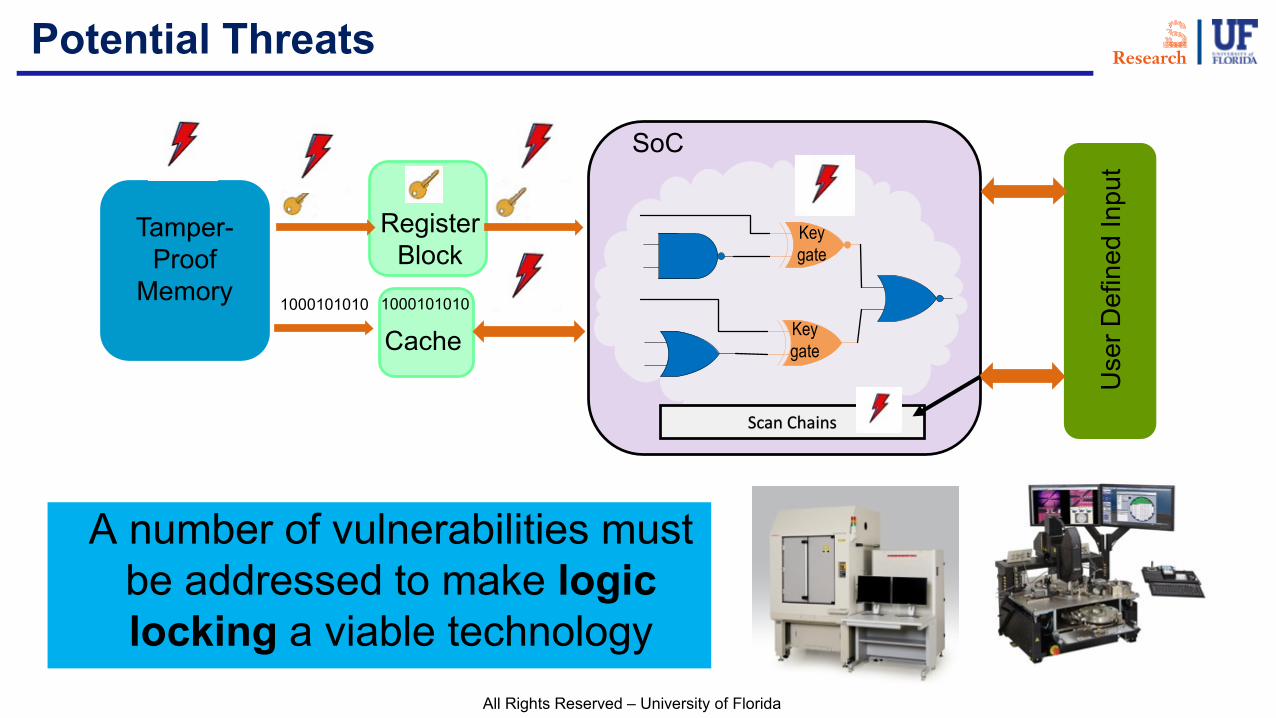
1000101010
Cache
Potential Threats
Tamper-Proof
Memory
Register Block
Use
r Def
ined
Inpu
t
1000101010
SoC
Key gate
Key gate
A number of vulnerabilities must be addressed to make logic locking a viable technology
Scan Chains
All Rights Reserved – University of Florida
Defense-in-Depth To defend a system against any particular attack using several
independent methods
14

All Rights Reserved – University of Florida
Defense-in-Depth for Protecting Obfuscation
15
KeyL1L1 L2L2 L3L3 L4L4 L5L5
All Rights Reserved – University of Florida
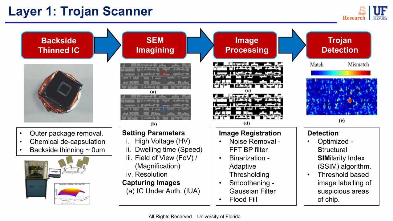
Layer 1: Trojan Scanner
Backside Thinned IC
SEM Imagining
Image Processing
Trojan Detection
• Outer package removal.• Chemical de-capsulation• Backside thinning ~ 0um
Setting Parametersi. High Voltage (HV)ii. Dwelling time (Speed)iii. Field of View (FoV) /
(Magnification)iv. Resolution
Capturing Images(a) IC Under Auth. (IUA)
Image Registration• Noise Removal -
FFT BP filter• Binarization -
Adaptive Thresholding
• Smoothening -Gaussian Filter
• Flood Fill
Detection• Optimized -
Structural SIMilarity Index (SSIM) algorithm.
• Threshold based image labelling of suspicious areas of chip.

All Rights Reserved – University of Florida
Protect Assets

All Rights Reserved – University of Florida
Asset: A resource of value worth protecting from an adversary
Source: Intel
Security Assets in SoCs:On-device keys (developer/OEM)Device configurationManufacturer FirmwareApplication softwareOn-device sensitive dataCommunication credentialsRandom number or entropyE-fuse, PUF, and more…
18
Security Assets

All Rights Reserved – University of Florida
Protect Assets: Strong Algorithms, Weak ImplementationStrong
Algorithm & Architecture
Weak Implementation &
Execution
Algorithms, architectures, and policies could be impacted by design methods that do not
understand Security!
Accesses/attack surfacesRemote Access (E.g., WiFi, Ethernet, Zigbee, etc.)PCB Access (E.g., JTAG and Debug ports)Physical Access
Vulnerabilities• Information Leakage• Side Channel Leakage• Fault Injection• IP Tampering, Trojan Insertion

All Rights Reserved – University of Florida
Gate Level -- Information Leakage
Modeling an asset as a stuck at fault Utilize automatic test pattern generation algorithms to detect that faultA successful detection → Existence of information flow
20
We need to identify all observe points →Asset can be observed

All Rights Reserved – University of Florida
Confidentiality Analysis
TakeawaysAll implementation of AES, RSA and PRESENT encryption modules have vulnerability due to DFT insertionThe ‘Distance’ and ‘Stimulus’ quantitative measure of vulnerability
Higher value less vulnerable
21
EncryptionAlgorithm
Design Seq.Elements
ObservablePoints
Distance Stimulus
Min Max Min Max
AEShigh speed 10769 2 2 3 5 7small area 2575 4 2 2 6 6
ultra-high speed 6720 2 0 1 2 3Single-DES small area 64 32 11 15 15 17
Triple-DES small area 128 48 10 12 29 33high speed 8808 2 2 2 3 3
RSA basic 555 32 4 3 6 6PRESENT light ware 149 2 2 2 3 3

All Rights Reserved – University of Florida
Power Side Channel AttacksNovember 4, 2020

All Rights Reserved – University of Florida
Block Leakage Analysis

All Rights Reserved – University of Florida
Security Rule Check
24
Experimental Security Validation4
Development ofSecurity Rules and Metrics
2
Establishing Secure Design Infrastructure
1
AR
CH
S
3 Development of Security-aware Automated CAD Tools

All Rights Reserved – University of Florida
Security Rule Check
25
Objective: Provide automated security assessment and possible countermeasures of given designs for target vulnerabilities
RTL Gate Layout
RTL level ARCHS
(ARCHS-R)
Gate level ARCHS
(ARCHS-G)
Layout level ARCHS
(ARCHS-L)
Trojan Insertion Vulnerability
Assessment (TIVA)Information
Flow Security (IFS)
MicroprobingVulnerability Assessment
Outcomes: Comprehensive set of formally defined transaction rules with security guarantees and data protection
Security Rules & MetricsUser Input and Constraints

All Rights Reserved – University of Florida
Chip Backside Is A New Backdoor• Frontside: Multiple interconnect layers
obstruct the optical path to transistor devices
• Backside: Active devices are directly accessible
Photon Emission
Laser Stimulation/Fault Injection
Optical Contactless Probing
Source: C. Boit et. al.
Hamamatsu PHEMOS - 1000

All Rights Reserved – University of Florida
Attacking Bitstream Encryption of FPGAs
JTAGBBRAM / eFuse
FPGA
AES DecryptorNVMAES Encryptor
…
Design
Encryptedbitstream
10111001010
Bitstream
010101…
• Device under Test (DUT): Xilinx Kintex 7 development board• Chip’s technology: 28 nm• No chip preparation (e.g., depackaging, silicon polishing, etc.)
• Optical Setup: Hamamatsu PHEMOS-1000• Laser wavelength: 1.3 𝜇𝜇m• Laser spot size: >1 𝜇𝜇m
• Non-destructive• Non-invasive• No Footprint

All Rights Reserved – University of Florida
Localizing the Configuration Logic
Xilinx Kintex 7 in flip-chip package Image acquisition with a infra-red laser scanning microscope
Tajik, S., Lohrke, H., Seifert, J. P., & Boit, C. "On the Power of Optical Contactless Probing: Attacking Bitstream Encryption of FPGAs," In Proceedings of the 2017 ACM SIGSAC Conference on Computer and Communications Security.

All Rights Reserved – University of Florida
Localizing the Configuration Logic
Random Logic

All Rights Reserved – University of Florida
Localizing Decryption Core using EOFM
Main CoreAES Core
Clock activity for unencrypted bitstream

All Rights Reserved – University of Florida
Localizing Decryption Core using EOFM
Main CoreAES Core
Clock activity for encrypted bitstream
All Rights Reserved – University of Florida
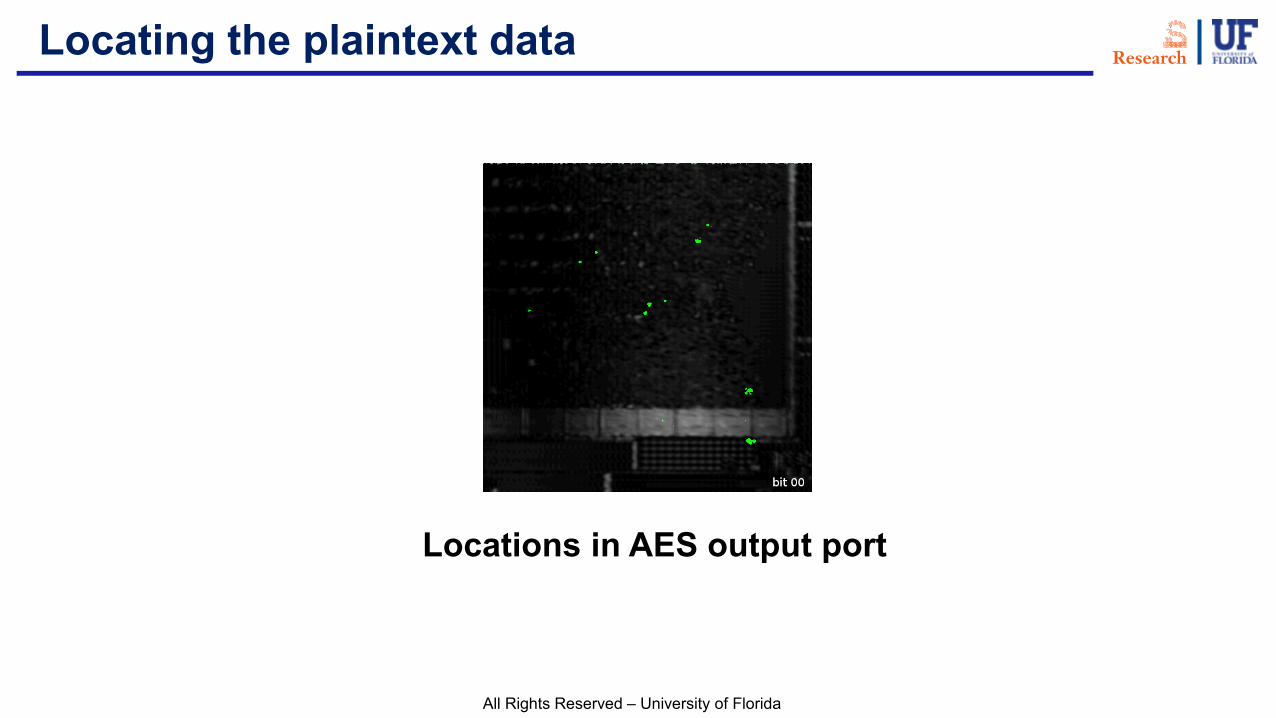
Locating the plaintext data
Locations in AES output port

All Rights Reserved – University of Florida
Key Extraction
BBRAM / eFuse
FPGA
AES DecryptorNVM
Encryptedbitstream
10111001010
Bitstream
010101…
OBIRCH(TLS)
key = 0xd781b86f274630b561f39c9736f512eb
0adf714f0d5c836c7a76ff627aca4923
• Protection• Circuit Level Solutions
• Device Level solutions
• Material Level Solutions
Target Nets Shield Nets

All Rights Reserved – University of Florida
Protect the Supply Chain
All Rights Reserved – University of Florida
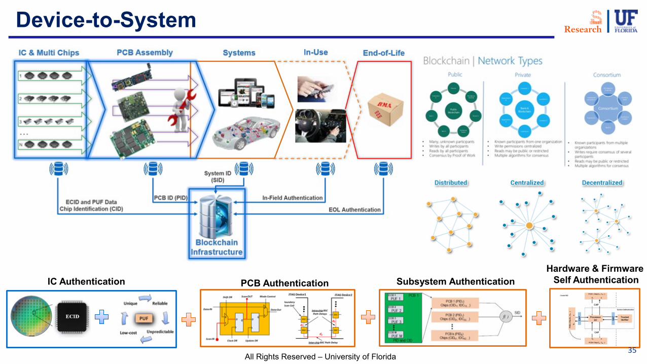
Device-to-System
35
IC Authentication PCB Authentication Subsystem AuthenticationHardware & Firmware
Self Authentication
35

All Rights Reserved – University of Florida
OCM: Enrollment & Ownership Release
36

All Rights Reserved – University of Florida
PCB Assembler: Verification & Ownership Acquire
37

All Rights Reserved – University of Florida
AutoBoM: External Visual Inspection of PCB
Optical Microscopy
Image Pre-processing
Bill of Material• Chips• Resistors• Capacitors• Ports
Analysis and Defect Recognition• Chips• Discrete Components• Solder• Contacts• PCB
Intelligent Microscopy for even lower time/cost!
Smart phone w/ adapter

All Rights Reserved – University of Florida
X-ray CT• Parameter Optimization
• Sample Preparation and Filtering
Image Processing and Segmentation• Separate Layers• Traces• Vias w/ Pads• Vias w/ Anti-Pads• Conductive Planes
CAD File Generation• Vectorization• PCB CAD File (PCB, DWG, DXF, etc..)
PCB Analysis• Trace timing• Signal integrity• Power integrity• Electromagnetic Interference
• Thermal Footprint• Security vulnerabilities
Auto3D: Internal Inspection of PCB
Nondestructive!
Slices

All Rights Reserved – University of Florida
Non-destructive Reverse Engineering

All Rights Reserved – University of Florida
SCAN Lab at FICS Research Institute
Florida Institute for Cybersecurity (FICS) Research

42
• Designed-in security• Standards: Logic Locking, SCA, Backside,
Provenance, Traceability
• Automation• Reduce complexity & cost
• Design with life cycle in mind• Device Systems
• Traceability & provenance
Recommendations

43
• Powerful but low cost inspection
• Hardware upgrade Zero day
• Smart devices DT for secure semiconductors
Recommendations

44
?