hardware architecture of the cell broadband engine ...kemper/cs654/slides/cellweiwei.pdf · between...
TRANSCRIPT
LOGO
Hardware Architecture of the Cell Broadband Engine Processor
Presented by Wei Wei, 04/20/2009
The CELL/B.E. processor
The Cell Broadband Enginee (Cell/B.E.) processor is the first implementation of a new multiprocessor family conforming to the Cell Broadband Engine Architecture (CBEA)
The CBEA and the Cell/B.E. processor are the result of a collaboration between Sony, Toshiba, and IBM known as STI, formally begun in early 2001
Although the Cell/B.E. processor is initially intended for applications in media-rich
consumer-electronics devices such as game
consoles and high-definition televisions, the architecture
has been designed to enable fundamental advances in processor performance
and supports a broad range of compute-intensive applications.
Cell/B.E. Basic Concepts
Compatibility with IBM 64b Power Architecture™Builds on and leverages IBM investment and community
Increased efficiency and performance, especially on media-rich applicationsAttacks on the “Power Wall”
• Heterogeneous Multiprocessor• High design frequency @ a low operating voltage with advanced power management
Attacks on the “Memory Wall”• Streaming DMA architecture• 3-level Memory Model: System memory, Local Store, Register Files
Attacks on the “Frequency Wall”• Highly optimized implementation• Large shared register files and software controlled branching to allow deeper pipelinesReal time responsiveness to the user and the network
Challenges: Real-time and security in a multiprocessor environmentApplicable to a wide range of platforms
Multi-OS support, including RTOS / non-RTOS

Comparison with traditional processors
Intel Tulsa (Xeon MP 7100 series)424mm2, 3.4 GHz@150W2 Cores, ~54 SP GFlops
Cell/B.E.175 mm², 3.2 GHz@60-80W
9 Cores, ~230 SP GFlops
Cell/B.E. vs traditional approaches
½ the space & power
consumption & much higher performance
Please note, both processors use the 65nm process.
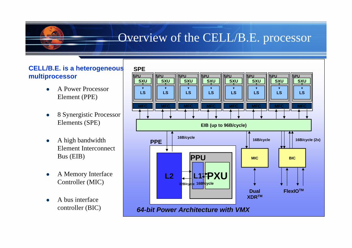
Overview of the CELL/B.E. processor
A Power Processor Element (PPE)
8 Synergistic Processor Elements (SPE)
A high bandwidth Element Interconnect Bus (EIB)
A Memory Interface Controller (MIC)
A bus interface controller (BIC)
16B/cycle (2x)16B/cycle
BIC
FlexIOTM
MIC
Dual XDRTM
16B/cycle
EIB (up to 96B/cycle)
64-bit Power Architecture with VMX
PPE
SPE
LS
SXUSPU
MFC
PXUL1
PPU
16B/cycleL2
32B/cycle
LS
SXUSPU
MFC
LS
SXUSPU
MFC
LS
SXUSPU
MFC
LS
SXUSPU
MFC
LS
SXUSPU
MFC
LS
SXUSPU
MFC
LS
SXUSPU
MFC
CELL/B.E. is a heterogeneousmultiprocessor
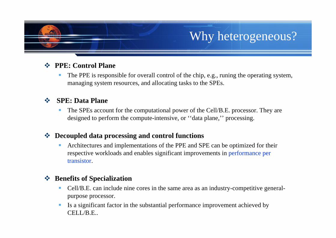
Why heterogeneous?
PPE: Control PlaneThe PPE is responsible for overall control of the chip, e.g., runing the operating system, managing system resources, and allocating tasks to the SPEs.
SPE: Data PlaneThe SPEs account for the computational power of the Cell/B.E. processor. They are designed to perform the compute-intensive, or ‘‘data plane,’’ processing.
Decoupled data processing and control functionsArchitectures and implementations of the PPE and SPE can be optimized for their respective workloads and enables significant improvements in performance per transistor.
Benefits of SpecializationCell/B.E. can include nine cores in the same area as an industry-competitive general-purpose processor. Is a significant factor in the substantial performance improvement achieved by CELL/B.E..
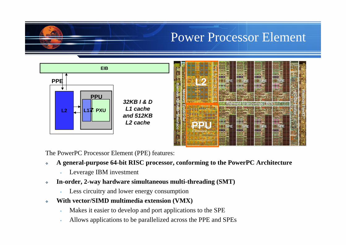
Power Processor Element
The PowerPC Processor Element (PPE) features: A general-purpose 64-bit RISC processor, conforming to the PowerPC Architecture
Leverage IBM investment In-order, 2-way hardware simultaneous multi-threading (SMT)
Less circuitry and lower energy consumptionWith vector/SIMD multimedia extension (VMX)
Makes it easier to develop and port applications to the SPEAllows applications to be parallelized across the PPE and SPEs
EIB
32KB I & D L1 cache
and 512KB L2 cache
PPE
PXUL1
PPU
L2
L2
PPU
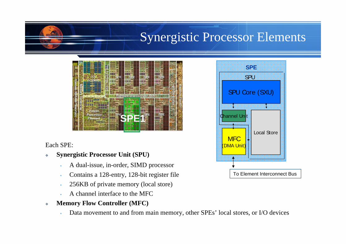
Synergistic Processor Elements
SPE1
SPU Core (SXU)
Channel Unit
Local StoreMFC
(DMA Unit)
SPU
SPE
To Element Interconnect Bus
Each SPE:Synergistic Processor Unit (SPU)
A dual-issue, in-order, SIMD processorContains a 128-entry, 128-bit register file256KB of private memory (local store)A channel interface to the MFC
Memory Flow Controller (MFC)Data movement to and from main memory, other SPEs’ local stores, or I/O devices
SIMD Architecture in Cell/B.E.
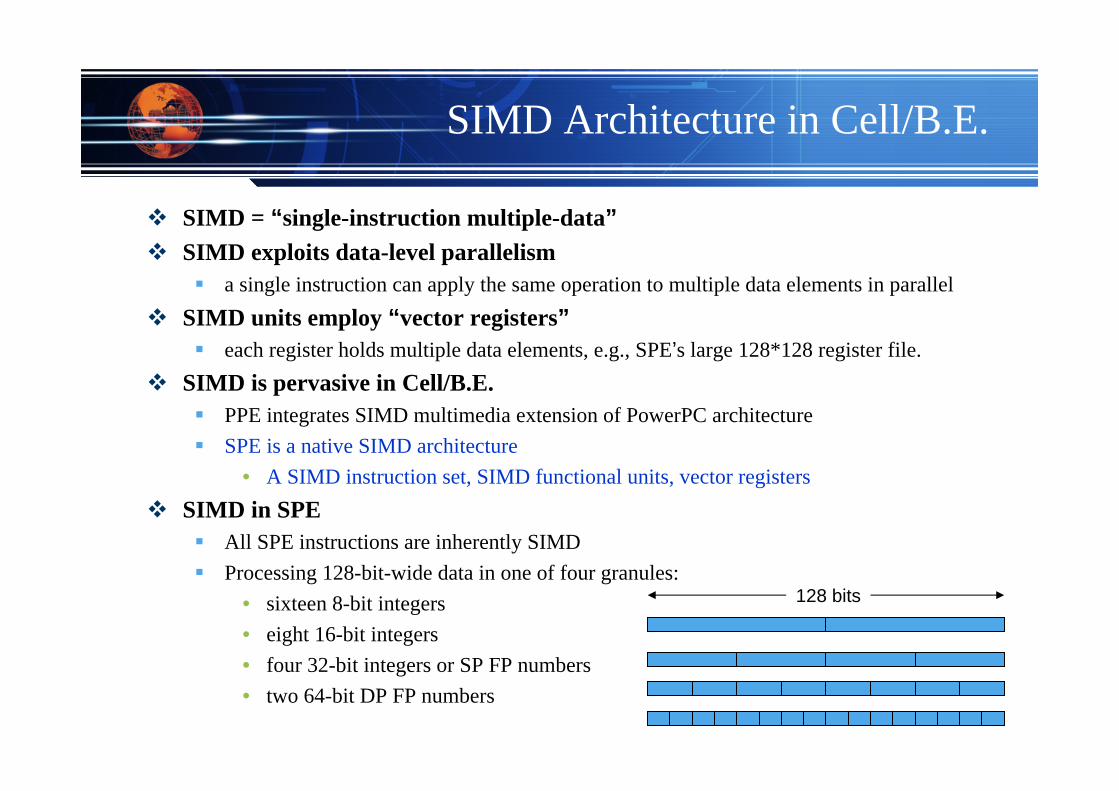
SIMD = “single-instruction multiple-data”SIMD exploits data-level parallelism
a single instruction can apply the same operation to multiple data elements in parallelSIMD units employ “vector registers”
each register holds multiple data elements, e.g., SPE’s large 128*128 register file.SIMD is pervasive in Cell/B.E.
PPE integrates SIMD multimedia extension of PowerPC architectureSPE is a native SIMD architecture
• A SIMD instruction set, SIMD functional units, vector registers SIMD in SPE
All SPE instructions are inherently SIMDProcessing 128-bit-wide data in one of four granules:
• sixteen 8-bit integers• eight 16-bit integers• four 32-bit integers or SP FP numbers• two 64-bit DP FP numbers
128 bits
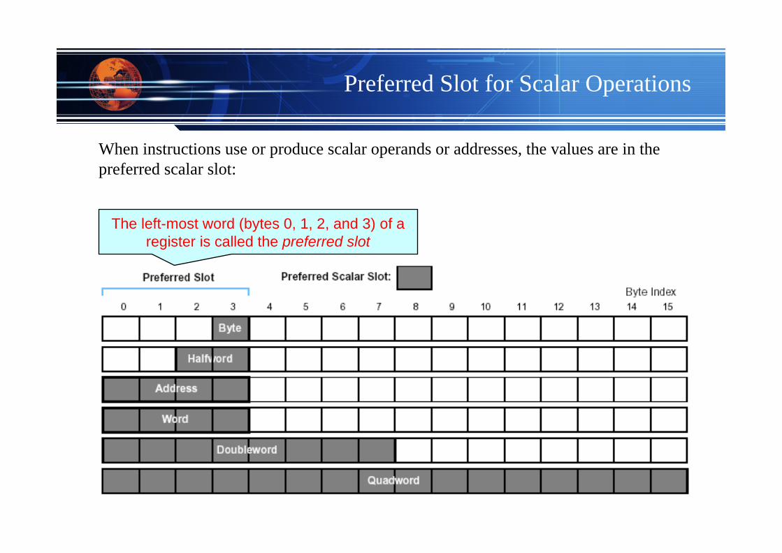
Preferred Slot for Scalar Operations
When instructions use or produce scalar operands or addresses, the values are in the preferred scalar slot:
The left-most word (bytes 0, 1, 2, and 3) of a register is called the preferred slot
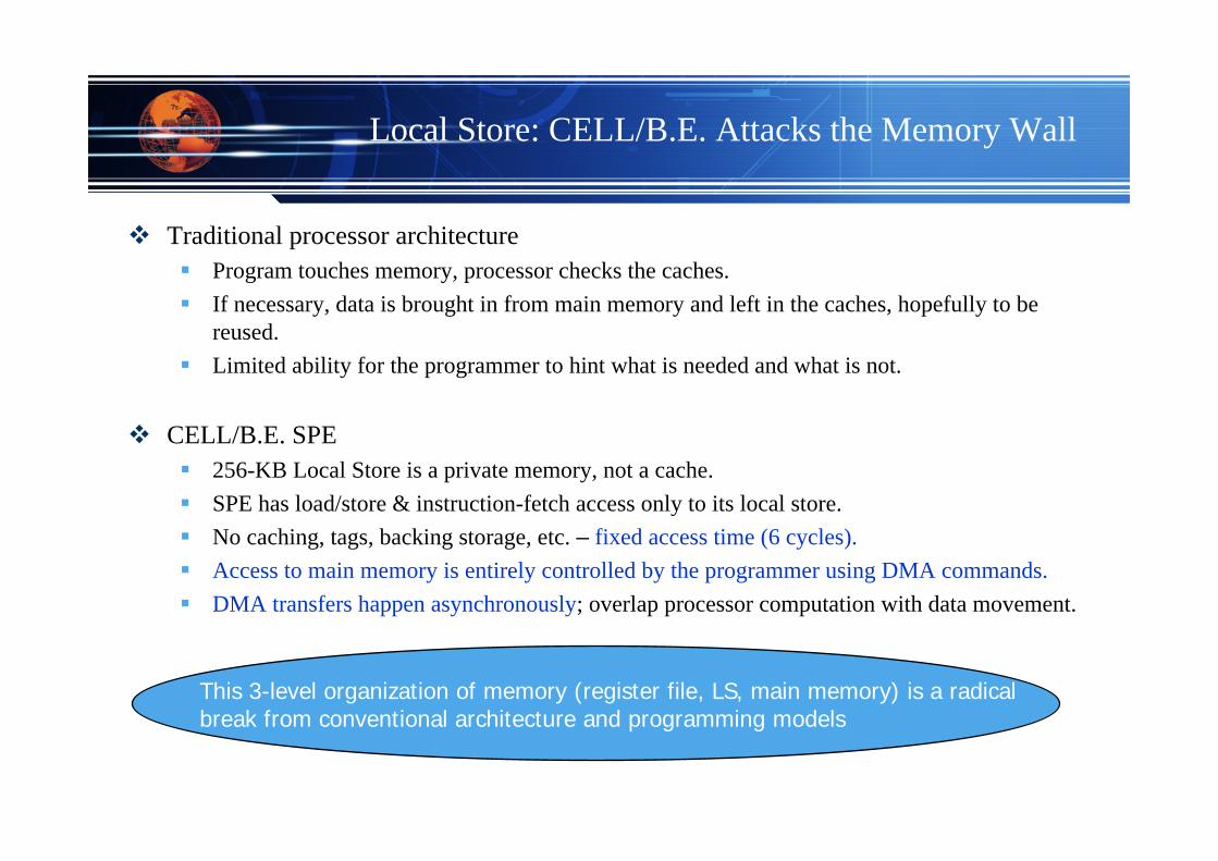
Local Store: CELL/B.E. Attacks the Memory Wall
Traditional processor architectureProgram touches memory, processor checks the caches.If necessary, data is brought in from main memory and left in the caches, hopefully to be reused.Limited ability for the programmer to hint what is needed and what is not.
CELL/B.E. SPE256-KB Local Store is a private memory, not a cache.SPE has load/store & instruction-fetch access only to its local store.No caching, tags, backing storage, etc. – fixed access time (6 cycles).Access to main memory is entirely controlled by the programmer using DMA commands.DMA transfers happen asynchronously; overlap processor computation with data movement.
This 3-level organization of memory (register file, LS, main memory) is a radical break from conventional architecture and programming models
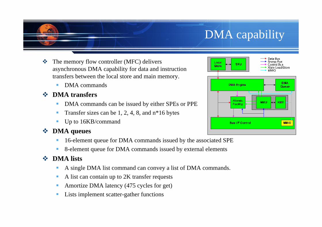
DMA capability
The memory flow controller (MFC) delivers asynchronous DMA capability for data and instruction transfers between the local store and main memory.
DMA commandsDMA transfers
DMA commands can be issued by either SPEs or PPETransfer sizes can be 1, 2, 4, 8, and n*16 bytesUp to 16KB/command
DMA queues16-element queue for DMA commands issued by the associated SPE8-element queue for DMA commands issued by external elements
DMA listsA single DMA list command can convey a list of DMA commands.A list can contain up to 2K transfer requestsAmortize DMA latency (475 cycles for get)Lists implement scatter-gather functions
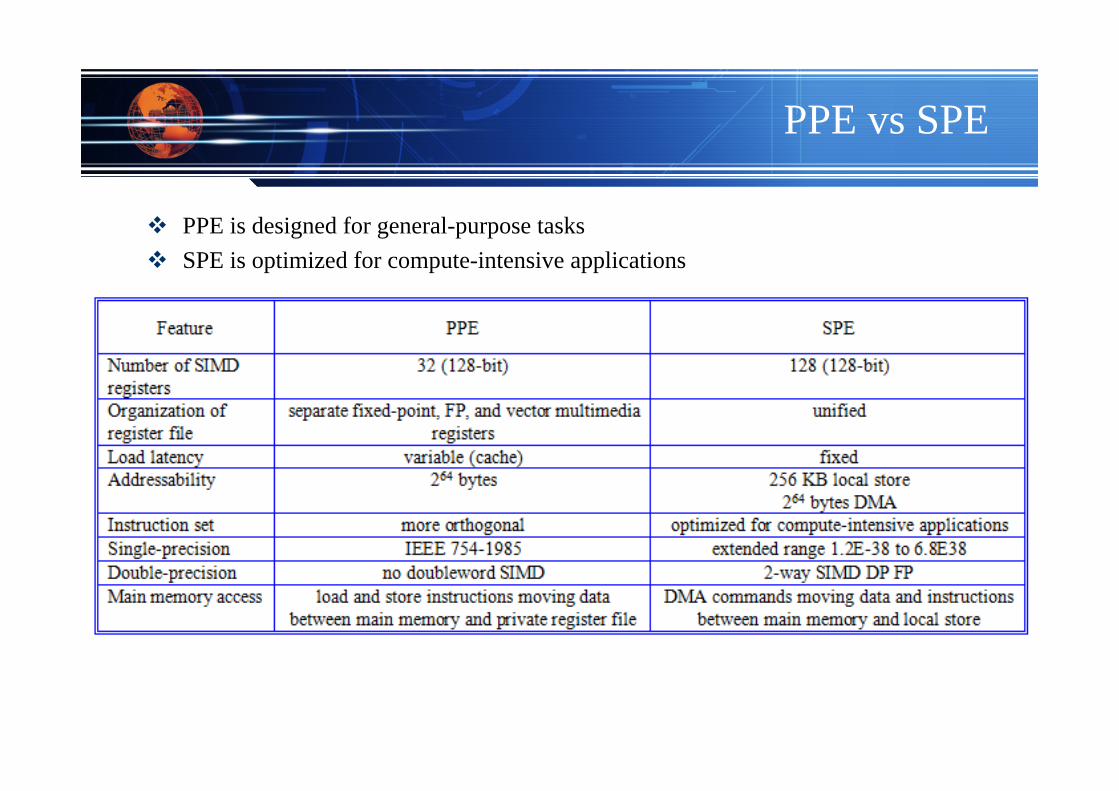
PPE vs SPE
PPE is designed for general-purpose tasksSPE is optimized for compute-intensive applications

Element Interconnect Bus
Interconnects 12 elementsFour 16-byte-wide unidirectional ringsEach ring supports up to three simultaneous data transfersTransfers occur at half the frequency of the processor, i.e., 96 bytes/cycle theoretical peak bandwidth
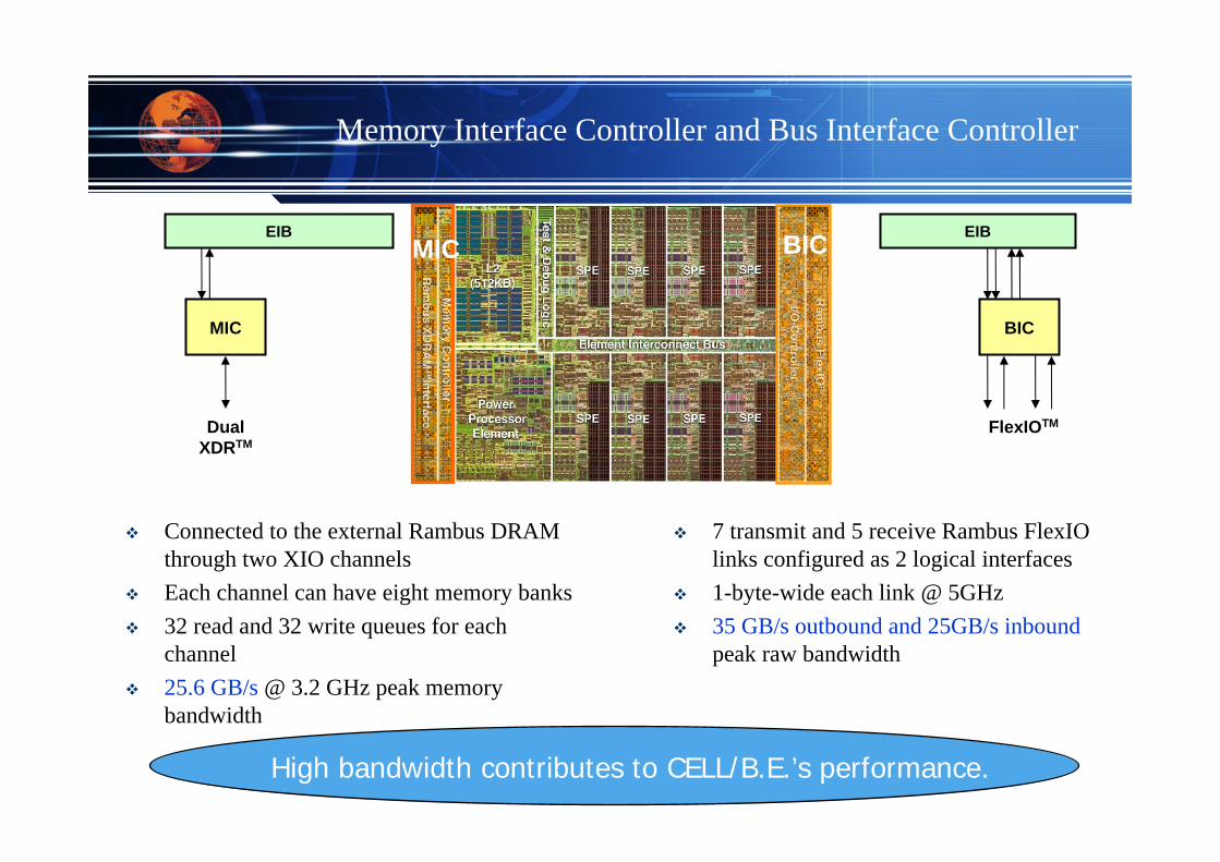
Memory Interface Controller and Bus Interface Controller
Connected to the external Rambus DRAM through two XIO channelsEach channel can have eight memory banks32 read and 32 write queues for each channel25.6 GB/s @ 3.2 GHz peak memory bandwidth
MIC
EIB
Dual XDRTM
BICMIC
7 transmit and 5 receive Rambus FlexIOlinks configured as 2 logical interfaces1-byte-wide each link @ 5GHz35 GB/s outbound and 25GB/s inboundpeak raw bandwidth
BIC
FlexIOTM
EIB
High bandwidth contributes to CELL/B.E.’s performance.
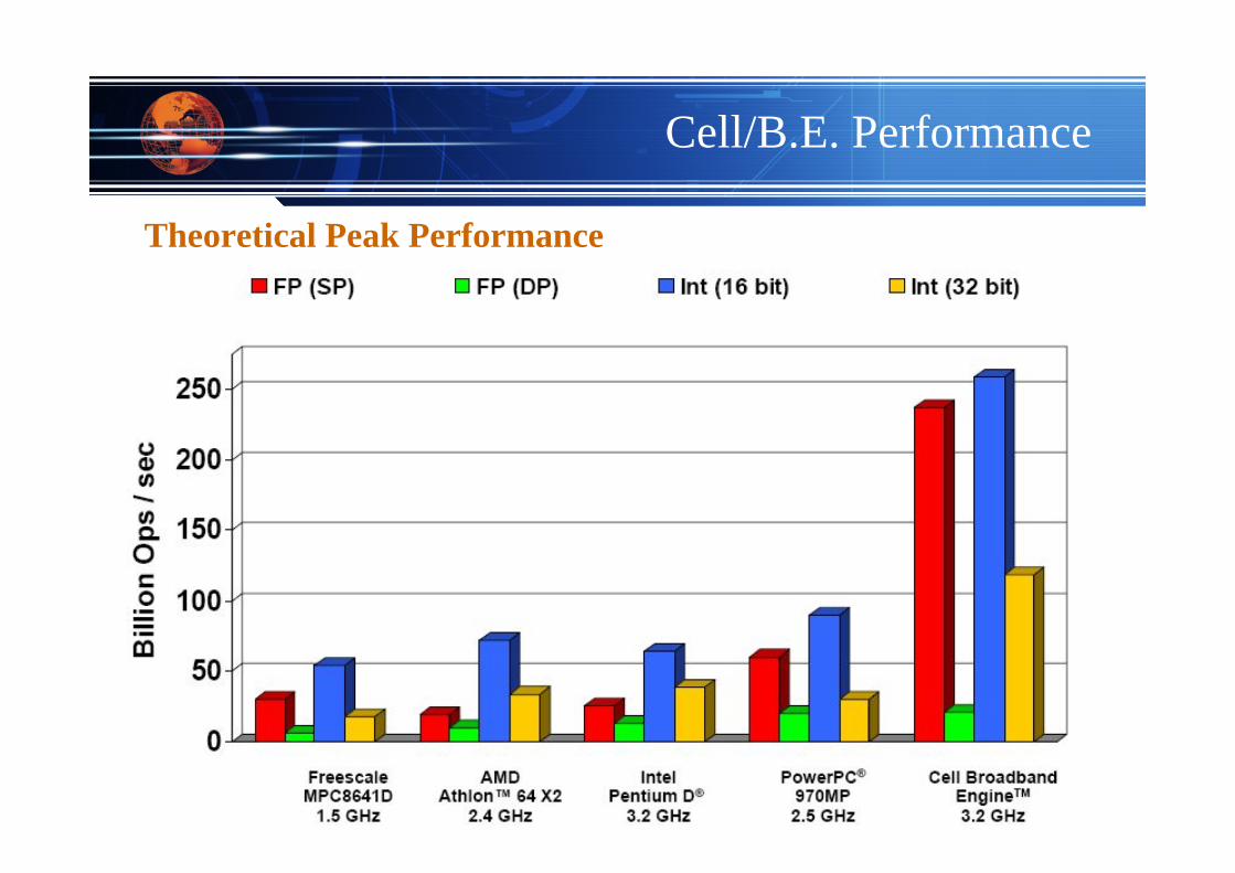
Cell/B.E. Performance
Theoretical Peak Performance
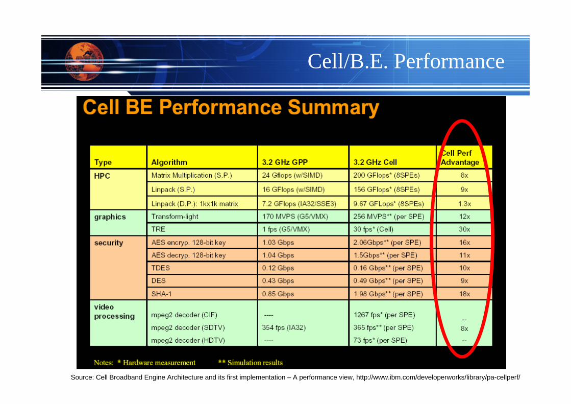
Cell/B.E. Performance
Source: Cell Broadband Engine Architecture and its first implementation – A performance view, http://www.ibm.com/developerworks/library/pa-cellperf/
Why is Cell/B.E. So Fast?
The SPE is a fast lean core optimized for compute-intensive processingEach SPE (3.2 GHz) is up to 3 times faster than the Pentium core (3.6 GHz) when computing FFTsThat is 24X better performance chip to chip
Parallel processing inside chip8 SPEs run concurrently
SpecializationPPE: Control PlaneSPE: Data Plane
High bandwidth205 GB/s sustained ring bandwidth 25.6 GB/s main memory bandwidth60 GB/s I/O bandwidth
High performance DMA transfersDMA transfers can be fully overlapped with core computationSoftware controlled DMA transfers can bring the right data into local store at the right time

Cell/B.E. Products
SCE PS3(Cell/B.E. + GPU)
IBM Cell/B.E. Blade
(2 Cell/B.E.s)
IBM Roadrunner(16,000 Cell/B.E.s
+ AMD)Sony Cell/B.E. Computing Unit
(Cell/B.E. + GPU + AV I/O)
Consumer ProfessionalHigh Perf
ComputingBusiness
Mercury Cell/B.E. PCI Card
(Cell/B.E. + Network)
Common Operating Systems, Infrastructure, Tools, Libraries, Code…
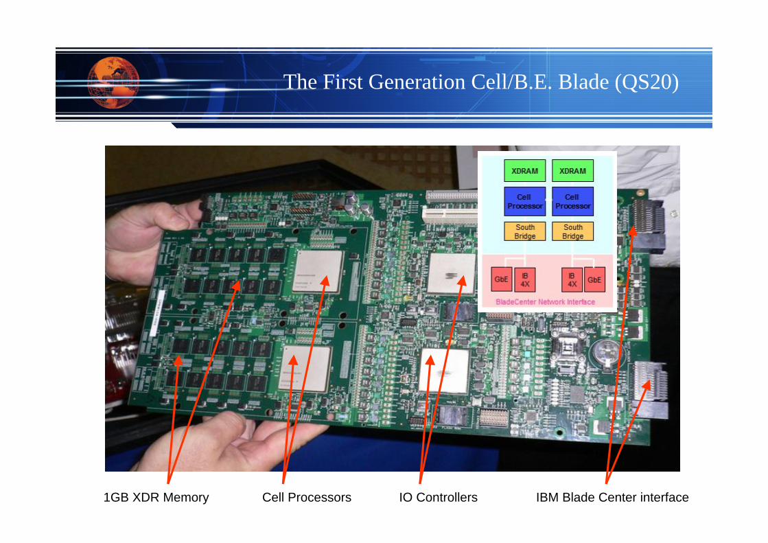
The First Generation Cell/B.E. Blade (QS20)
Cell Processors1GB XDR Memory IO Controllers IBM Blade Center interface
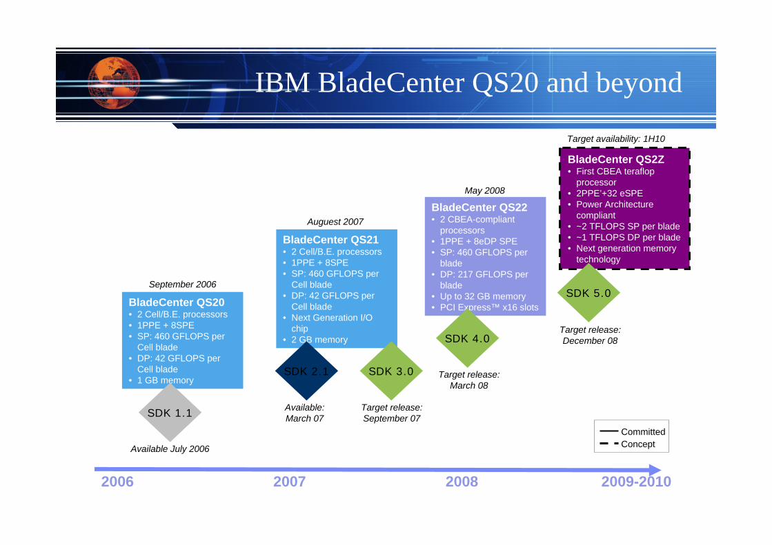
IBM BladeCenter QS20 and beyond
2006 20082007 2009-2010
BladeCenter QS20• 2 Cell/B.E. processors • 1PPE + 8SPE• SP: 460 GFLOPS per
Cell blade• DP: 42 GFLOPS per
Cell blade• 1 GB memory
BladeCenter QS21• 2 Cell/B.E. processors • 1PPE + 8SPE• SP: 460 GFLOPS per
Cell blade• DP: 42 GFLOPS per
Cell blade• Next Generation I/O
chip• 2 GB memory
BladeCenter QS22• 2 CBEA-compliant
processors • 1PPE + 8eDP SPE• SP: 460 GFLOPS per
blade• DP: 217 GFLOPS per
blade• Up to 32 GB memory• PCI Express™ x16 slots
SDK 1.1
SDK 2.1 SDK 3.0
SDK 4.0
September 2006
Auguest 2007
May 2008
Available July 2006
Available:March 07
Target release:September 07
Target release:March 08
BladeCenter QS2Z• First CBEA teraflop
processor• 2PPE’+32 eSPE• Power Architecture
compliant• ~2 TFLOPS SP per blade• ~1 TFLOPS DP per blade• Next generation memory
technology
Target availability: 1H10
SDK 5.0
Target release:December 08
ConceptCommitted
Thank you!