hardware acceleration for image...
TRANSCRIPT

Hardware acceleration for imageprocessing
Semester projectJanuary 2008, EPFL, I&C, BIRGAuthor Lukas BendaSupervisors Pierre-André MudryProf. Auke Ijspeert

ii

iii

Contents
1 Introduction 12 Methods 3
2.1 Image processing . . . . . . . . . . . . . . . . . . . . . . . . . . . . 32.2 Hardware . . . . . . . . . . . . . . . . . . . . . . . . . . . . . . . . 5
2.2.1 Material used . . . . . . . . . . . . . . . . . . . . . . . . . . 62.3 Sliding window architecture . . . . . . . . . . . . . . . . . . . . . . 8
2.3.1 Three images lines FIFO . . . . . . . . . . . . . . . . . . . . 92.3.2 Image border copy . . . . . . . . . . . . . . . . . . . . . . . 92.3.3 5x5 processing window . . . . . . . . . . . . . . . . . . . . . 9
2.4 Communication and memory management . . . . . . . . . . . . . . 102.4.1 Register transfers . . . . . . . . . . . . . . . . . . . . . . . . 112.4.2 DMA transfers . . . . . . . . . . . . . . . . . . . . . . . . . 112.4.3 Parameters transfer . . . . . . . . . . . . . . . . . . . . . . 12
2.5 Processing primitives . . . . . . . . . . . . . . . . . . . . . . . . . . 132.5.1 Implemented primitives . . . . . . . . . . . . . . . . . . . . 132.5.2 Gaussian �lter . . . . . . . . . . . . . . . . . . . . . . . . . 152.5.3 Gradient image . . . . . . . . . . . . . . . . . . . . . . . . . 182.5.4 Median/Min/Max �lter . . . . . . . . . . . . . . . . . . . . 212.5.5 Canny edge detector . . . . . . . . . . . . . . . . . . . . . . 24
2.6 C Program . . . . . . . . . . . . . . . . . . . . . . . . . . . . . . . 292.6.1 Communication with the FPGA . . . . . . . . . . . . . . . 292.6.2 Image processing . . . . . . . . . . . . . . . . . . . . . . . . 292.6.3 OpenCV . . . . . . . . . . . . . . . . . . . . . . . . . . . . . 29
3 Results 313.1 Global comparison . . . . . . . . . . . . . . . . . . . . . . . . . . . 323.2 Relative comparison . . . . . . . . . . . . . . . . . . . . . . . . . . 343.3 Hardware time analysis . . . . . . . . . . . . . . . . . . . . . . . . 35
4 Conclusion 374.1 Future work . . . . . . . . . . . . . . . . . . . . . . . . . . . . . . . 37
4.1.1 External RAM memory . . . . . . . . . . . . . . . . . . . . 374.1.2 Larger processing window . . . . . . . . . . . . . . . . . . . 374.1.3 Processing immediately after reception . . . . . . . . . . . . 38
5 Acknowledgments 41References 43
iv

List of Figures
2.1 Image representations . . . . . . . . . . . . . . . . . . . . . . . . . 42.2 Image processed by a sliding window. The convolution is given here
as an example of processing primitive. . . . . . . . . . . . . . . . . 52.3 Global architecture of the system . . . . . . . . . . . . . . . . . . . 62.4 A Virtex II FPGA similar to the one used in this project . . . . . 62.5 A Logitech QuickCam Web . . . . . . . . . . . . . . . . . . . . . . 72.6 Hardware architecture of the sliding window . . . . . . . . . . . . . 82.7 Image border copy for di�erent sizes of processing window . . . . . 102.8 FPGA usage for the sliding window . . . . . . . . . . . . . . . . . 102.9 Architecture including a block RAM memory . . . . . . . . . . . . 112.10 Software image division . . . . . . . . . . . . . . . . . . . . . . . . 122.11 Operators design . . . . . . . . . . . . . . . . . . . . . . . . . . . . 132.12 FPGA usage for an Operator unit . . . . . . . . . . . . . . . . . . 142.13 FPGA usage for Operator unit (containing four operator unit) . . 142.14 Gaussian distribution with mean (0,0) and σ = 1 . . . . . . . . . . 152.15 Gaussian discrete kernel . . . . . . . . . . . . . . . . . . . . . . . . 152.16 Gaussian �lter convolution . . . . . . . . . . . . . . . . . . . . . . . 162.17 Gaussian �lter example . . . . . . . . . . . . . . . . . . . . . . . . 162.18 FPGA usage for the Gaussian �lter . . . . . . . . . . . . . . . . . . 172.19 Gradient function approximation . . . . . . . . . . . . . . . . . . . 182.20 Gaussian discrete kernel . . . . . . . . . . . . . . . . . . . . . . . . 182.21 Gaussian �lter convolution . . . . . . . . . . . . . . . . . . . . . . . 192.22 Gradient image example . . . . . . . . . . . . . . . . . . . . . . . . 192.23 FPGA usage for the Gradient �lter . . . . . . . . . . . . . . . . . . 202.24 Architecture for sorting 3 pixels . . . . . . . . . . . . . . . . . . . . 212.25 System global architecture . . . . . . . . . . . . . . . . . . . . . . . 222.26 Median �lter example . . . . . . . . . . . . . . . . . . . . . . . . . 222.27 FPGA usage for C2 (two pixel comparator) . . . . . . . . . . . . . 232.28 FPGA usage for C3 (three pixel comparator) . . . . . . . . . . . . 232.29 FPGA usage for median �lter . . . . . . . . . . . . . . . . . . . . 232.30 Canny edge detector algorithm . . . . . . . . . . . . . . . . . . . . 242.31 Possible directions for the gradient phase . . . . . . . . . . . . . . 242.32 Simpli�ed phase calculations . . . . . . . . . . . . . . . . . . . . . 252.33 Hardware schema computing the phase . . . . . . . . . . . . . . . . 252.34 FPGA usage for gradient Magnitude and Phase . . . . . . . . . . . 262.35 Example of non-maxima elimination for a particular pixel . . . . . 262.36 Hardware schema for non-maxima elimination . . . . . . . . . . . . 272.37 FPGA usage for Non-maxima elimination . . . . . . . . . . . . . . 272.38 Canny edge detector steps . . . . . . . . . . . . . . . . . . . . . . . 282.39 Cone and rodes sensitivities . . . . . . . . . . . . . . . . . . . . . . 30
v

3.1 openCV functions processing time . . . . . . . . . . . . . . . . . . 323.2 Hardware processing time . . . . . . . . . . . . . . . . . . . . . . . 323.3 Processing times . . . . . . . . . . . . . . . . . . . . . . . . . . . . 333.4 Processing times relatively to a hardware monopass processing time 343.5 Subdivision of hardware processing time . . . . . . . . . . . . . . . 353.6 Subdivision of hardware processing time . . . . . . . . . . . . . . . 353.7 FPGA usage for the whole system . . . . . . . . . . . . . . . . . . 364.1 Processing times . . . . . . . . . . . . . . . . . . . . . . . . . . . . 38
vi

vii

viii

Chapter 1
Introduction
Today images are more and more part of our everyday life. We use cell phones,webcams and high resolution cameras and we can modify our photos on our com-puter. In industry this trend is visible as well, very often combined with some sortof image processing. We can see security systems identifying cars' licence plates,character recognition systems to recognize addresses on letters as well as medicalimagery we can �nd in hospitals.
The goal of this semester project is to obtain a hardware acceleration systemfor image processing. There are essentially two reasons to implement this kindof processing in a hardware way : speed and implementation in an embeddedsystem. Speed up image processing can be very useful for real-time processingimages coming form a camera. This way we avoid heavy processing with a genericmicroprocessor. Embedding this system can be useful in many �elds, like visionin robotics or a monitoring system.
The idea here is mainly to obtain a system faster than software image pro-cessing. The �nal user should be able to process a stream of images coming froma video camera with a simple call to a set of C functions. The link with hard-ware has to stay invisible to the user. The framework stays limited to grayscaleimages with constant size is going to implement several kinds of �ltering (Gaus-sian blur, median/min/max �lter, gradient image and a Canny edge detector).These operators are based on a 3 by 3 pixels wide sliding window similarly toconvolution.
The system is going to run on a Xilinx FPGA communicating with the com-puter through the PCI port. In order to test and compare the results with soft-ware image processing, the whole process is going to be compared to openCVfunctions [5].
1

2
Chapter 2
Methods
2.1 Image processing
There are di�erent kinds of images and many di�erent processing methods we canapply to an image. We can distinguish three kind of images.
Binary imagesBinary images, where a pixel is black or white. These images are mostly used formorphology processing, the main operators are dilatation and erosion. �The gameof life� is a well known example of this kind of processing.
Greyscale imagesGreyscale images where a pixel is de�ned by an intensity level between black andwhite (included). Theses images are used if we are interested in the shape ofobjects present in the image. There are many operators that can be applied onthese images, like a simple Gaussian blur, an edge detector or a sophisticated facerecognition system.
Color imagesThe last kind of image used in image processing are color images, where a pixel isde�ned as a triplet of intensities of red, green and blue. These images can be seenas a group of three grey images. The processing applied on these images concernsessentially colors, like white balancing, color region classi�cation, etc ...
In this project we choose to work only with grey images which is a good com-plexity compromise between binary and color images. We also needed to choosethe kind or family of operators that we want to apply on our images. Some oper-ators, like histogram equalization, need global informations about the image, likethe min/max pixel of the whole image. Others operations need only partial orlocal information about the image, for example convolution only needs to knowthe currently processed pixel's neighborhood. Operators can also be more com-plex and need several computational steps, for example edge detection discussedlater. We choose to use only operators that use a windowing system, which meansthat we only need to know the currently processed pixel and it's neighborhood.Convolution is a window operation, but there are window operations that are not
3

(a) Binary image (b) Grey image (c) Color image
Figure 2.1: Image representations
convolutions. There is the complete list of the operators choose to be implementedin our project :
• Identity operator• Gaussian blur• Gradient image• Median �lter• Canny edge detectorAll these operators will be discussed later in detail.The approach of image processing using a processing window is described in
�gure 2.2 :The processing window (PW) slides on the image and a speci�c processing is
applied to every pixel. The resulting pixel depends on the operator, the processedpixel and its neighborhood. Of course we need to choose the size of our processingwindow. It can be between 0 and the size of our image. We choose a 3 by 3pixels PW which is simple to handle. Of course a bigger PW is more powerful,but requires more computation, or more precisely a longer delay as our primitivesare made in a combinatorial way.
We mentioned the neighborhood of the currently processed pixel. We realizethat this neighborhood is not de�ned for pixels on the corners or edges of theprocessed image, because the neighborhood is �outside� of the image. Di�erentapproaches are used to solve this problem. We can simply set the unde�ned pixelsto a constant value, for example black. Another way is to imagine the image as atorus, the top edge linked to the bottom edge and the left side linked to the rightside. The adopted solution was to set the unde�ned neighbor pixel to the samegray value as the currently processed pixel.
Convolution is a widely used operation based on a PW and we give it in�gure 2.2 as an example. Each pixel of the current PW is multiplied by thecorresponding �pixel� of the convolution kernel, which is of the same size as thethe PW. The results of these multiplications are summed up to obtain the resulting
4

Figure 2.2: Image processed by a sliding window. The convolution is given hereas an example of processing primitive.
pixel. Once the operation is done the PW �slides� on the next pixel. Convolutioncan be described by the following formula :
X(m,n) = I(m,n)×H(m,n) =J−1∑j=0
K−1∑k=0
H(j, k)I(m− j, n− k) j, k ∈ {0, 1, 2}
In the �gure above, the current pixel is A11, its neighborhood are the pixelsAxy and the convolution kernel is Hxy.
2.2 Hardware
In the previous section we described the theoretic approach to process an image.Now we want to implement this system on hardware keeping in mind that ourgoal is speed gain. A lot of design choices had to be done. There is also a lot oflimitations linked to hardware that are not present in software image processing.That is what we are going to discuss now.
The general architecture of the whole system is shown in �gure 2.2.In order to show our results on a real-time application we choose to use as
input a continuous �ow of images provided by a webcam. Here we had the choiceto connect the webcam directly to the FPGA that contains the image processingsystem and sends directly the result to the computer or to connect the camerato the computer, store the image in the computer memory and only then tosend it to the FPGA. We choose the second approach because we want to makeperformance comparisons between hardware and software computational speed.The whole system is controlled through a C program. This way we can create aninterface that hides the hardware part to the programmer.
5
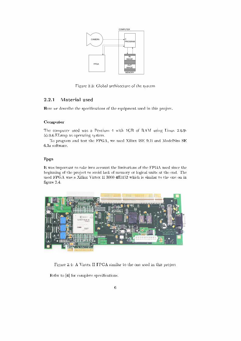
Figure 2.3: Global architecture of the system
2.2.1 Material used
Here we describe the speci�cations of the equipment used in this project.
ComputerThe computer used was a Pentium 4 with 1GB of RAM using Linux 2.6.9-55.0.6.ELsmp as operating system.
To program and test the FPGA, we used Xilinx ISE 9.1i and ModelSim SE6.3a software.
FpgaIt was important to take into account the limitations of the FPGA used since thebeginning of the project to avoid lack of memory or logical units at the end. Theused FPGA was a Xilinx Virtex II 3000-4�1152 which is similar to the one on in�gure 2.4.
Figure 2.4: A Virtex II FPGA similar to the one used in this projectRefer to [4] for complete speci�cations.
6

CameraWe used the Logitech QuickCam Web. It provides color images of size 356 by 292pixels.
Figure 2.5: A Logitech QuickCam Web
Comparative softwareAnthony Edward Nelson [1] has done a project similar to ours, the results wereabout 100 times slower, but the work was done in 2000 and the architecture usedless hardware. In his work the comparison between hardware and software resultswas done using Matlab. Unfortunately, Matlab is not designed for fast real-timeimage processing. We choose to use the openCV [5] library. OpenCV not onlyallows very fast real-time image processing, but is also written in C, which allowsus to run our processing functions and openCV processing functions in the sameC program and make more precise comparisons.
OpenCV also provides very useful input/output functions that we need in anycases. We use openCV functions to acquire images from the camera. Plottingfunctions are not necessary, but are very useful for tests.
7

2.3 Sliding window architecture
The �gure 2.2 shows the theoretical approach of image processing using a slidingprocessing window. Now we want to apply this theoretical model to a hardwarearchitecture.
As we will see later, the communication between the computer and the FPGAis the speed bottleneck of the whole system. For this reason we want to transferthe minimum amount of data. In [1] only the nine pixels of the PW were stored inthe FPGA. Using this approach, after each �slide� of the PW, 3 new pixels werered from the image and three pixels were forgotten. This means that after theprocessing of the whole image each pixel was read three times and it representsa lot or redundant transfers, but the register usage was small. If a 5 by 5 pixelswindows was used each pixel would be read �ve times.
To avoid these redundant transfers we chose to permanently store three linesof the image. The PW slides from left to right on the central line. When itcomes at the right end, a new line is red and the oldest line is forgotten. Theseforgotten pixels will newer be used again and each pixel of the image is red onlyonce. Of course this approach implies much higher amount of registers on theFPGA. Figure 2.6 illustrates this approach :
Figure 2.6: Hardware architecture of the sliding windowIn order to use a standard word length for the PCI transfers, we wanted to
handle pixels using 32 bits long words. As each pixel has a value between 0 and255 and is stored on 8 bits, we process pixels by packets of four. Due to this factwe process always four pixels paralellry. It is why we have four identical processing
8
primitives on the previous schema. Due to this fact, we create a constraint on thesize of our input image which has to have a length which is a multiple of four.There is no constraint on the image height.
2.3.1 Three images lines FIFO
Unlike in the theoretical version, the hardware PW doesn't slide on the pixellines, but the pixels are shifted under the PW. After several versions, the simplestand fastest way to implement the three lines system was to use three large inter-connected FIFOs. The input pixels are pushed in the �rst FIFO and the poppedpixels are the ones processed by the PW. A state machine separates the processinginto three stages.
First stage : �ll the FIFOsFirst we need to wait until all the FIFOs are full. At this stage there is only input.No output and no processing.
Second stage : main processingSecond we can begin to process the image. At this stage we read one input pixelunit, we process it and we get an output as result. The whole is done in one clockcycle. This is another constraint on our processing primitives, each operation hasto be done in one clock cycle. We will see the impact of this constraint later.
Last stage : empty the FIFOsIn the third and last stage, most of the image was already processed and there isno more input to read, because the whole image was red, but the FIFOs are stillfull. In this stage we process and output pixel units until the FIFOs are empty.
2.3.2 Image border copy
As we told above the approach used to manage the unde�ned neighborhood, wasto copy the borders. Here we separate the problem into horizontal and verticalborders. The corners are taken into account in the horizontal part. To managethe borders, we use a vertical and a horizontal counter to know which part of theimage we are processing. The horizontal copy is performed if we are processingthe �rst or the last line of the image. In this case we use multiplexers to copy the�rst or the last line twice as we can see in �gure 2.6.
This way the neighborhood pixels of the �rst and the last line are explicitlyinside the FIFO. Concerning the vertical borders, those are not inside the FIFO,but they are implicitly computed by the PW depending on the vertical counter.This is the best approach we found to reduce complexity and memory usage.
2.3.3 5x5 processing window
Even if this functionality wasn't implemented, it is interesting to consider thechanges necessary to use a 5 by 5 PW to show the scalability of our system. Weneed three modi�cations. First we need �ve lines of the image instead of three,which requires more registers, but is still feasible using our FPGA. The second
9
(a) 3x3window
(b) 5x5window
Figure 2.7: Image border copy for di�erent sizes of processing window
thing to do is the copy of a border of two pixels instead of a border of one pixelas we can see in �gure 2.7.
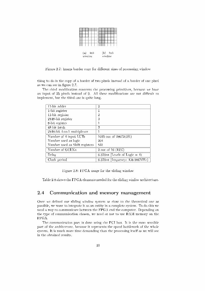
The third modi�cation concerns the processing primitives, because we havean input of 25 pixels instead of 9. All these modi�cations are not di�cult toimplement, but the third one is quite long.
11-bit adder 21-bit register 111-bit register 22848-bit register 38-bit register 148-bit latch 32848-bit 4-to-1 multiplexer 1Number of 4 input LUTs 1035 out of 28672(3%)Number used as logic 204Number used as Shift registers 831Number of GCLKs 2 out of 16 (12%)Delay 6.370ns (Levels of Logic = 4)Clock period 6.370ns (frequency: 156.986MHz)
Figure 2.8: FPGA usage for the sliding windowTable 2.8 shows the FPGA elements needed for the sliding winfow architecture.
2.4 Communication and memory management
Once we de�ned our sliding window system as close to the theoretical one aspossible, we want to integrate it as an entity in a complete system. To do this weneed a way to communicate between the FPGA end the computer. Depending onthe type of communication chosen, we need or not to use RAM memory on theFPGA.
The communication part is done using the PCI bus. It is the most sensiblepart of the architecture, because it represents the speed bottleneck of the wholesystem. It is much more time demanding than the processing itself as we will seein the obtained results.
10

We have the choice between using simple register transfers or DMA bursttransfers. Here we implemented both approches to allow comparisons.
2.4.1 Register transfers
This type of transfer is much easier to implement than the DMA transfer, so it wasimplemented �rst to allow tests on the whole system. The problem here is thatwe can transfer only one 32 bit word at the same time. Each transfer of this kindneeds to open the PCI bus, perform the transfer and then close the PCI bus. Allthis has to be done once per a pixel unit, which is 4 pixels. This approach is veryslow because of the numerous openings/closings of the PCI port. On the otherhand, using using this technique, we don't need to use any additional memory. Weonly �ll the three lines and the resulting output pixels are directly send the resultback to the computer. We don't need to modify the schema, because the inputand output pixels are directly connected to the PCI bus. Once these transferswere working we could �nish the processing part of the project and test the wholesystem very fast, but the speed results were clearly unsatisfying and we had tomodify our approach.
2.4.2 DMA transfers
As the goal of this project was speed, DMA transfers became necessary. Thisway the PCI bus was opened and closed only once per image, and the speed oftransfer became one 32 bit word by clock cycle. The implementation was basedon an example code given by Alpha-Data [3]. Using this approach and unlike theregister transfer, we needed to store the whole image in the FPGA memory beforeprocessing. The memory management is shown in �gure 2.9.
Figure 2.9: Architecture including a block RAM memoryHere the memory used to store the image is again a simple FIFO. Using this
architecture we need three stages. First, during the incoming DMA transfer, the
11

FIFO is �lled up with the complete input image. There is no processing at thisstage. Once the image is inside the FIFO the second stage begins. We pop pixelsinside the processing unit, perform processing and we push them back inside thesame FIFO. The multiplexer chooses to push input pixels in the FIFO if we arein the �rst stage and result pixels if we are in the second stage. Once the wholeimage is processed, which means that the FIFO contains only processed pixelscomes the third stage where the content of the FIFO is transferred back to thecomputer.
Unfortunately, here we reach the limits of our FPGA. Even if the amount ofRAM memory is just su�cient to contain a 356 by 292 pixels wide image, we arenot allowed to generate a single FIFO large enough for the whole image. A �rstapproach to solve this problem would be to generate a large FIFO by connectingtwo smaller ones. We suppose this would be the fastest way to solve the problem,but here we reach memory space limits of our FPGA. To solve this problem andat the same time show the scalability of our system, we choose to �cut� the inputimage using software and we send two half of the image and process it as twoseparated images. If we use a bigger image it's easy to extend this approach tomore image divisions. Once the two images are processed and send back to thecomputer, we need to connect them to provide the real output image. To do thiswe have to manage borders and process the middle line of the image twice as isshown in �gure 2.10.
Figure 2.10: Software image divisionAs we said if we use a bigger image, we can divide it in more than two parts,
but this approach slows the system down.2.4.3 Parameters transfer
We don't only need to transfer the image to be processed. The hardware alsoneeds to know which kind of processing we want to apply (Gaussian, median, ...).To do this we had the choice to use register transfer for the arguments and DMAtransfer for the image. This solution would avoid to attach a header to each imageat the software level. At the other hand if we need to send a lot of arguments, itwould slow down the system. The chosen approach was to attach a header in asoftware way, perform a single DMA transfer and then separate the image fromthe header inside the FPGA.
12

2.5 Processing primitives
This part concerns the image processing itself and describe in detail all the pro-cessing primitives. First we give elements of image processing theory and then weexplain their hardware implementation. Each primitive is followed by an outputimage example and the number of necessary logical units used by the FPGA toimplement the primitive.2.5.1 Implemented primitives
Identity Returns the input image, used for testsGaussian �lter Smooths the imageMedian/Min/Max Filter Removes 'Salt and pepper' noise preserving edgesGradient �lter Returns the gradient imageCanny edge detector Returns thin edges of the image
The whole computational unit �Operators� is compsed of four �Operator� units.This way we can process four pixels in a parallel way. A single �Operator� unitcontains each of the primitives described above. This is shown in Figure 2.11.
Figure 2.11: Operators designTables 2.12 and 2.13 describe the FPGA usage of the �Operator� and �Opera-
tors� modules.
13

10-bit adder 1111-bit adder 811-bit subtractor 412-bit adder 113-bit adder 29-bit adder 102-bit latch 113-bit comparator greater 26-bit comparator greatequal 16-bit comparator greater 88-bit comparator less 182-bit 3-to-1 multiplexer 1Number of 4 input LUTs 806 out of 28672(2%)Delay 38.088ns (Levels of Logic = 63)
Figure 2.12: FPGA usage for an Operator unit10-bit adder 4411-bit adder 3211-bit subtractor 1612-bit adder 413-bit adder 89-bit adder 402-bit latch 413-bit comparator greater 86-bit comparator greatequal 46-bit comparator greater 328-bit comparator less 722-bit 3-to-1 multiplexer 4Number of 4 input LUTs 3206 out of 28672(11%)Delay 38.409ns (Levels of Logic = 64)
Figure 2.13: FPGA usage for Operator unit (containing four operator unit)
14

2.5.2 Gaussian �lter
The Gaussian �lter is a convolution operator which is used to blur images andremove noise. In the continuous domain, we can �nd it for a certain σ through :
G(x, y) =1
2πσ2e−
x2+y2
2σ2
which looks like :
Figure 2.14: Gaussian distribution with mean (0,0) and σ = 1
For our purpose use we will use a discrete version of this kernel with a 3x3window :
Figure 2.15: Gaussian discrete kernelFigure 2.16 shows the hardware implementation of the Gaussian �lter we de-
signed:
15
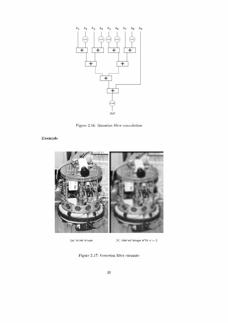
Figure 2.16: Gaussian �lter convolution
Exemple
(a) Input image (b) blurred image with σ = 2
Figure 2.17: Gaussian �lter example
16

FPGA usage
10-bit adder 311-bit adder 212-bit adder 19-bit adder 2Number of 4 input LUTs 64 out of 28672(∼0%)Delay 19.867ns (Levels of Logic = 20)
Figure 2.18: FPGA usage for the Gaussian �lter
17

2.5.3 Gradient image
The gradient of an image is essentially used for edge detection in image processing.The idea is to �rst �nd the horizontal and vertical derivatives of an image, thismeans regions in the image where the di�erence of intensity of close pixels. Forthis reason the �lter is very sensitive to noise and we usually apply a Gaussianblur before using this operator. The �lter is de�ned by the following operation :
5A =δI
δx+
δI
δy= (Hx ×A) + (Hy ×A)
Then we can obtain the gradient magnitude :|∇A| =
√(Hx ×A)2 + (Hy ×A)2
And the gradient direction :θ(∇A) = arctan
(Hx ×A
Hy ×A
)The gradient magnitude is often approximated by :
|∇A| = |Hx ×A|+ |Hy ×A|
(a) real function (b) Approximated function
Figure 2.19: Gradient function approximationWe will also use this approximation in our hardware implementation in order
to reduce complexity. The convolution kernel used is the Sobel operator :
Figure 2.20: Gaussian discrete kernel
18

The following schema shows the hardware implementation of the gradient im-age we designed:
Figure 2.21: Gaussian �lter convolution
Exemple
(a) Input image (b) Gradient image
Figure 2.22: Gradient image example
19

FPGA usage
10-bit adder 411-bit adder 312-bit subtractor 29-bit adder 4Number of 4 input LUTs 113 out of 28672(∼0%)Delay 20.565ns (Levels of Logic = 16)
Figure 2.23: FPGA usage for the Gradient �lter
20

2.5.4 Median/Min/Max �lter
This operator is a bit di�erent from Gaussian �lter and gradient image becauseit is not a convolution. Here the idea is to sort the pixels of the current window.There are three possibilities of �ltering with this approach. We can always takethe median value, or always take the minimum value or always take the maximumvalue. Depending on this choice, the output image will be the following :
Min Erosion of the features of the imageMax Dilatation of the features of the imageMedian Flattening of the image
'Salt and pepper' noise removal
For our purpose we don't need to sort completely the nine pixels of our window.All we need to know is the min, max and median pixel. It is relatively easy tosort n2 pixels in a hardware fashion, but here we have 9 pixels. To solve thisproblem, we �rst de�ne a comparator C3 that sorts 3 pixels and is assembled ofthree binary comparators C2. This architecture is shown in the next �gure :
Figure 2.24: Architecture for sorting 3 pixelsUsing only six of these comparators, and a multiplexer to select the min/max/median
value, we are not able to implement a 9 pixel sorter, but it is su�cient for ourneeds, because we �nd the min/max and median value. The 'X' represent theremaining unsorted pixels.
21

Figure 2.25: System global architecture
Example
(a) Input image (withnoise)
(b) Median �lter 3x3 (c) Median �lter 5x5
Figure 2.26: Median �lter example
22
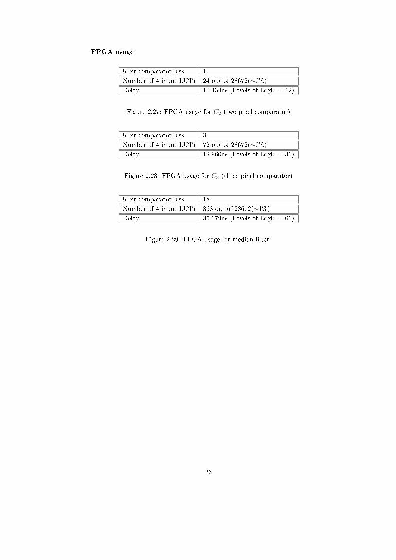
FPGA usage
8-bit comparator less 1Number of 4 input LUTs 24 out of 28672(∼0%)Delay 10.434ns (Levels of Logic = 12)
Figure 2.27: FPGA usage for C2 (two pixel comparator)
8-bit comparator less 3Number of 4 input LUTs 72 out of 28672(∼0%)Delay 19.960ns (Levels of Logic = 31)
Figure 2.28: FPGA usage for C3 (three pixel comparator)
8-bit comparator less 18Number of 4 input LUTs 368 out of 28672(∼1%)Delay 35.179ns (Levels of Logic = 61)
Figure 2.29: FPGA usage for median �lter
23

2.5.5 Canny edge detector
This operator is here to show the usage of a multi-pass �lter. An detailed expla-nation of this algorithm can be found in [2]. The popular Canny edge detectoruses the following steps to �nd contours presents in the image.
Figure 2.30: Canny edge detector algorithmThe �rst stage is achieved using our Gaussian smoothing. The resulting image
is send to the PC that sends it back to the gradient �lter, but here we modi�ed ourgradient �lter a bit because this time we don't only need the gradient magnitudethat is given by our previous operator, but we need separately Gx and Gy. Wealso need the phase or orientation of our gradient which is obtained using thefollowing formula :
θ = arctan
(Gy
Gx
)As we can see this equation contain an arctan and a division. These operators
are very di�cult to implement using hardware. We also don't need a high preci-sion. The �nal θ has to give only one of the four following possible directions, aswe can see on Figure 2.31. The fourth direction is the horizontal direction withzero degrees, not indicated on the �gure.
Figure 2.31: Possible directions for the gradient phaseArctan and the division can be eliminated by simply comparing Gx and Gyvalues. If they are of similar length, we will obtain a diagonal direction, if one
is at last 2.5 times longer than the other, we will obtain a horizontal or verticaldirection. The �gure 2.32 shows this idea.
24

Figure 2.32: Simpli�ed phase calculationsHere we can see a new problem. For the next stage, non-maxima elimination,
we need two informations, the magnitude and the phase at the same time. Oursystem is designed to process only one image at a time. The solution used herewas to store both informations on the same result image. Each possible 8bit pixelstores one of the four possible directions on two bits and the magnitude on the6 remaining bits. The price to pay is the lost of two bits of information of themagnitude. The �gure 2.33 shows the corresponding hardware schema, Table 2.34presents its FPGA usage.
Figure 2.33: Hardware schema computing the phase
25

10-bit adder 411-bit adder 311-bit subtractor 213-bit adder 29-bit adder 42-bit latch 113-bit comparator greater 22-bit 3-to-1 multiplexer 1Number of 4 input LUTs 168 out of 28672(∼0%)Delay 20.707ns (Levels of Logic = 16)
Figure 2.34: FPGA usage for gradient Magnitude and Phase
Non-maxima eliminationThe non-maxima elimination �lter is here to eliminate pixels that are not part ofa continuous line, like isolated pixels even if they have a high gradient magnitude.This technique allows to get ride of a lot of noise.
Figure 2.35: Example of non-maxima elimination for a particular pixelThe �gure 2.35 shows this principle. The Mx is the magnitude of the current
pixel. Ma and Mb are the magnitudes of the neighbor pixels perpendicular to thecurrent pixel's phase.
If (Mx > Ma) AND (Mx > Mb) we eliminate the current pixel, else we keepthe pixel. The �gure 2.36 shows the hardware implementation.
26

Figure 2.36: Hardware schema for non-maxima eliminationFor the last part, the edge detector uses only one threshold instead of the usual
two. But this is not adapted to hardware implementation.6-bit comparator greatequal 16-bit comparator greater 8Number of 4 input LUTs 59 out of 28672(∼0%)Delay 11.845ns (Levels of Logic = 12)
Figure 2.37: FPGA usage for Non-maxima elimination
27

Example
Figure 2.38: Canny edge detector steps
28

2.6 C Program
Three sets of C functions were used through this work. First the functions usedfor communication with the FPGA. Theses functions are not supposed to be usedby the �nal user. The image processing functions that are given to the user andperform calls to the hidden communication functions. Finally we used openCVfunctions for speed comparisons.
2.6.1 Communication with the FPGA
The initFPGA() is a modi�ed and modular version of the example program givenby Alpha-Data. It is called only once in the main() function. It allocates block ofmemory that will be used to communicate. The closeFPGA() frees the allocatedspace. Again it has to be called only once at the end of the main() function.Unfortunately these two functions are necessary and because of them the hardwaresystem is not as hidden as we wanted.
2.6.2 Image processing
The process_image(iin, iout, oper) function receives pointers to input/outputimages and operator type as arguments. We need to copy the input image in thespace allocated by initFPGA(). This is unfortunately a necessary step because wecan transfer only the block of memory allocated above. To transfer the operatortype (identity, Gaussian, ...) and its parameters (min, max or median for themedian �lter and threshold level for the canny edge detector)we �rst copy thisoperator as a header of the image at the beginning of the allocated memory andthen we copy the image itself.
The received resulting image don't need any header when it is transferred backto the computer.
2.6.3 OpenCV
First tests were not done on real images. We used small still images generated byhand. This way we could easily plot the resulting integer value of each pixel. Inorder to get an input image from the camera, we used cvCaptureFromCAM() andcvQueryFrame(). These functions �ve us a color image that has to be transformedinto a grey image. This conversion is done by simply taking the green value ofthe RGB image. Green is used because human sensitivity to green is very closeto the human sensitivity to light intensity as shows �gure 2.39 found in [7].
This is again a necessary software processing that has to be done once peracquisition. Fortunately for multipass primitives as Canny edge detector we don'tapply this operation between di�erent passes, but only before the �rst one, becauseafter the transformation we use the same grey image format.
To obtain an image plot as output we used cvShowImage(...) to test visuallylarge images.openCV image processingWe also used the following image processing functions to compare the processingspeed between hardware and software :
• cvSmooth(input, output, CV_GAUSSIAN, windowSize);
29
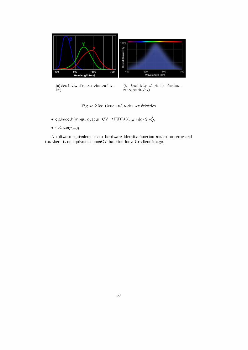
(a) Sensitivity of cones (color sensitiv-ity)
(b) Sensitivity of rhodes (lumines-cence sensitivity)
Figure 2.39: Cone and rodes sensitivities
• cvSmooth(input, output, CV_MEDIAN, windowSize);• cvCanny(...);A software equivalent of our hardware Identity function makes no sense and
the there is no equivalent openCV function for a Gradient image.
30
Chapter 3
Results
It is interesting to note that di�erent openCV functions need more or less pro-cessing time depending on their complexity. For example median �ltering is morecomplex and longer than gradient �ltering. With the FPGA this is not the case.The processing time is equivalent independently of the type of processing. Thisis due to our vhdl implementation constraint which says that any operator has toprocess a block of four pixels in one clock cycle. Knowing this we decided to showprocessing time for each software operator. For the hardware version we give thetime needed for di�erent parts of the processing: DMA transfer length, processinglength, etc ...
An interesting thing to note is that, if available, the Intel Integrated Perfor-mance Primitives(IPP) is used for lower-level operations for OpenCV [6]. In thecase tis option was activated, we were not comparing our system to pure softwareprocessing but to a hardware accelerated software. Unfortunately did not manageto verify if the openCV hardware acceleration was available or activated.
31

3.1 Global comparison
In Figure 3.1 we present processing times of the software implementation of ourprimitives. The name of the primitive is followed by NxN which is the size of theprocessing window. These times are shown in blue in the bar plot of Figure 3.3and are preceded by the mention �soft_XXX�. On the same graph, the resuls areof our hardware implementation using DMA transfers are shown in green andpreceded by the mention �hard_XXX�. The exact times are shown in Figure 3.2.
hard_complete time needed for the whole processinghard_in time needed for incoming DMA transferhard_out time needed for out DMA transferhard_prcessing time needed for image processing
The red bar on the right, �hard_register� is the performance of our hardwareversion implementing register transfers.
Every given time lengths are given in milliseconds[ms].median 7x7 median 5x5 median 3x3 gauss 7x7 gauss 5x5 gauss 3x3 canny0.051606 0.040798 0.013219 0.007561 0.004694 0.003877 0.004051
Figure 3.1: openCV functions processing time
processing transfer IN transfer OUT complete using complete usingDMA transfer register transfer
0.000746 0.001206 0.001302 0.003725 0.054165
Figure 3.2: Hardware processing timeThe �gure 3.3 gives a global comparison between processing using openCV
software, hardware with DMA transfers and hardware with register transfers.
32

Figure 3.3: Processing times
33

3.2 Relative comparison
The �gure 3.4 shows the software and register transfer results of Figure 3.3. Thistime the vertical axis unit is the time needed for a �hard_complete� processing.For example a median �lter using a 7x7 wide processing window takes about 14times more processing time than a hardware primitive using DMA transfers.
Figure 3.4: Processing times relatively to a hardware monopass processing time
34

3.3 Hardware time analysis
In order to analyze more deeply the hardware version using DMA transfers, �g-ure ?? gives time percentage for a full monopass processing. We can see thatthe speed bottleneck of our system is the transfer of data. The �software part�shown here is here because we want to take into account all the software process-ing needed by our hardware system. This processing includes the arrays copiesdiscussed above, image header formatting, image division, etc . . .
processing transfer IN transfer OUT software0.000746 0.001206 0.001302 0.000471
Figure 3.5: Subdivision of hardware processing time
Figure 3.6: Subdivision of hardware processing timeFigure 3.7 shows the �nal usage of the FPGA needed for the whole project.
35

10-bit adder 4411-bit adder 3411-bit subtractor 1612-bit adder 413-bit adder 814-bit adder 115-bit addsub 130-bit subtractor 232-bit adder 19-bit adder 4014-bit up counter 332-bit up counter 21-bit register 8911-bit register 2128-bit register 115-bit register 12-bit register 122-bit register 12848-bit register 33-bit register 232-bit register 34-bit register 18-bit register 12-bit latch 448-bit latch 313-bit comparator greater 817-bit comparator less 131-bit comparator greatequal 131-bit comparator greater 131-bit comparator less 131-bit comparator lessequal 132-bit comparator less 36-bit comparator greatequal 46-bit comparator greater 328-bit comparator less 722-bit 3-to-1 multiplexer 42848-bit 4-to-1 multiplexer 132-bit 4-to-1 multiplexer 11-bit tristate bu�er 232-bit tristate bu�er 1Number of 4 input LUTs 4489 out of 28672(15%)Number used as logic 3913Number used as Shift registers 576Number of BRAMs 32 out of 96 (33%)Number of GCLKs 2 out of 16 (12%)Clock period 9.216ns (frequency: 108.502MHz)Delay 9.216ns (Levels of Logic = 13)
Figure 3.7: FPGA usage for the whole system
36

Chapter 4
Conclusion
For monopass image processing primitives, the results obtained using hardwarewith DMA transfer are faster than their software implementation. For mutipassprocessing this is not always the case, because of numerous transfers that remainthe bottleneck of our system. As the processing is really fast, it would be interest-ing to use much more complex processing primitives so that the transfers wouldbe just a small percentage of the whole process.
4.1 Future work
The results obtained using DMA transfers were satisfying because faster than thesoftware version. Anyway there are several possible ways to get a higher speedup.
4.1.1 External RAM memory
As we saw above, the speed bottleneck of the project are image transfers. Whenwe use a multipass primitive like the canny edge detector, the image is transferredthree times from the computer to the FPGA and back again. To reduce thenumber of transfers, we could use external RAM memory present on the board.This way we could store intermediate images directly on the FPGA instead oftransferring large amount of data several times between the computer and theFPGA. Here we suppose memory transfers are faster than DMA transfers, anassumption that should be tested.
4.1.2 Larger processing window
For this project we choose 3 by 3 pixel wide processing window. We can extendthis to 5 by 5 or 7 by 7 pixels wide window. Doing this we can apply more complexprocessing to our images, but the main advantage is again indirectly the speed up.As we have seen, the hardware processing time stays constant, this seems to betrue (but should be tested) even if we use a larger window. On the software side,it is much longer to process a larger window as we saw in the results chapter.
37

4.1.3 Processing immediately after reception
Another idea that could be interesting to test is to process pixels immediatelyafter their reception. This way we would not wait until the FIFO is �lled withthe incoming image before the processing as the actual implementation does. Do-ing this we could slightly reduce the processing time. Figure 4.1 illustrates thisprocess.
Figure 4.1: Processing times
38

39

40

Chapter 5
Acknowledgments
I would like to thank Pierre-André Mudry, the supervisor of this project as wellas Michel Ganguin, Julien Ru�n and Alessandro Crespi for their great help onthis project.
41

42

Bibliography
[1] Anthony Edward Nelson, 2000, Implementation of image processing algorithmson FPGA hardware, Vanderbilt University.
[2] Dmitrij Csetverikov, Basic Algorithms for Digital Image Analysis: a course,Eötvös Loröand University, Budapest, Hungary.
[3] ADM-XRC SDK 4.8.0 User Guide (Win32).[4] Xilinx, 2005, Virtex-II Platform FPGAs: Complete Data Sheet.[5] Vadim Pisarevsky, 2000, Introduction to OpenCV, Intel Corporation, Software
and Solutions Group.[6] Changsong Shen, Sidney S. Fels and James J. Little, OpenVL: Towards
A Novel Software Architecture for Computer Vision, University of BritishColumbia.
[7] Human color vision :http://photo.net/photo/edscott/vis00010.htm
43

44

Appendix
The attached �les contain the vhdl and C code of the project as well as this �le.Vhdl �lescomp2.vhdcomp3.vhdcomp9.vhdgauss3x3grad3x3.vhdgradPM.vhdnonmax.vhdoperator.vhdoperators.vhdinput1.vhdddma-xrc.vhdimage_pack.vhdC �lesfpga.hfpga.copencv.hopencv.csimple.cMake�le
45