hae-moon seo realizing a cmos rf transceiver for wireless sensor
TRANSCRIPT

Realizing a CMOS RF Transceiver for Wireless Sensor Networks 1
Realizing a CMOS RF Transceiver for Wireless Sensor Networks
Hae-Moon Seo
X
Realizing a CMOS RF Transceiver for Wireless Sensor Networks
Hae-Moon Seo1, 2
1Korea Electronics Technology Institute (KETI), 2Kyungpook National University (KNU) South Korea
1. Introduction
The choice of the CMOS radio frequency (RF) transceiver architecture affects the design of the whole system and is thus a fundamental one. In order to make a good choice, several factors have to be considered, the most important ones being: performance, power consumption, die size, cost, integration level, and time-to-market. The minimum required performance is dictated by the IEEE802.15.4 standard approval. The relative weight of all other factors is determined by the wireless sensor network application at hand. As the RF transceiver developed here targets very small devices such as information-gathering nodes for sensor network applications, a small size and low power consumption are key requirements. In particular, as power consumption sets dimensions and type of the battery, it also has a major impact on size, weight, and cost of the system. In this chapter, we explore the implementation and testing of a fully CMOS integrated RF transceiver for wireless sensor networks in sub-GHz ISM-band applications. A comprehensive description of the radio system architecture, RF transceiver circuits, and measurement results is described in this sub-chapter. At the end of this chapter, a fully CMOS RF transceiver chip is presented to give an impression of the possible die size and floor plan for a highly integrated transceiver chip.
1.1 Introduction of Wireless Sensor Networks Recently, the desire for wireless connectivity has led an exponential growth in wireless communication. In particular, wireless sensor networks are potential wireless network applications for the following future ubiquitous computing system. Ubiquitous sensor networks are an emerging research area with potential applications in environmental monitoring, surveillance, military, health, and security (Y. K. Park et al. 2005), . The power dissipation of wireless sensor networks does require low power consumption for several years’ operation. There has been a great deal of interest in realizing low power, low cost, compact RF transceiver IC for wireless sensor networks. Several technological trends that are driving the technical evolution of wireless technology include the process scaling of CMOS transistors and higher bandwidth available at ISM bands. Almost all of the license free bands propose both linear and nonlinear modulation standards for wireless applications, and thus requiring different design optimizations in the RF transceiver. Along
1
www.intechopen.com

with these issues, there exists the challenge to develop fully integrated wireless solutions in silicon-based substrates (S. Sarkar et al., 2003).
2. The Radio System Architecture for Wireless Sensor Networks
Conventional transceiver architectures as shown in Fig.1 include heterodyne, zero-IF (intermediate-frequency), and low-IF conversion structure (P. S. Choi et al. (2003), C. Cojocaru et al. (2003), M. Valla et al. (2005), Ilku-Nam et al. (2003)), each having their own advantages and disadvantages. However, it becomes further challenging to meet all the specifications of many applications while keeping more competitiveness than the others. The super-heterodyne architecture is without any doubt the most often used transceiver topology and it has been in use for a long time already and its way of operating is very well known. It is the most widely used architecture, mainly because of its high performance. However, it usually requires image-reject and external channel selection filters and is therefore not well suited for fully integrated systems. Also, it has difficulties in the multi-band/mode transceiver and has problems of high power consumption, high cost. The low-IF and zero-IF architectures can achieve much better performance at low-power consumption and are well suited for high integration. The concept of the low-IF (P. S. Choi et al. (2003), C. Cojocaru et al. (2003)) starts from the survey that all information necessary to separate the mirror frequency from the wanted frequency is available in the two low frequencies after quadrature conversion. This scheme can avoid the DC offset problem and eliminate IF SAW and image RF filters. However, it suffers from impairments such as I/Q mismatching, even-order nonlinearity, and local oscillator (LO) pulling/leakage. Some calibration techniques for stringent image rejection may be used at the expense of additional complexity and power consumption. Finally, zero-IF (M. Valla et al. (2005), Ilku-Nam et al. (2003)) architecture performs a direct down-conversion of the wanted frequency to the baseband. The consequence is that the mirror signal is equal to the wanted frequency. This does however not mean that there would not be a mirror signal problem in the zero-IF receiver. But, this architecture remains the most suitable solution for high integration, low power consumption, and low cost. Moreover, it has advantage in elimination of image rejection requirements. However, it may suffer from impairments of DC offset, flicker noise, and complication of LO frequency-planning to evade LO pulling/leakage. The communication nodes for ubiquitous networks are required to be integrated in one die for low power consumption and low cost wireless sensor network applications. The overall wireless personal area networks (WPAN) system architecture is shown in Fig.2. It consists of the RF transceiver and a companion digital baseband (BB) processor, which implements both physical (PHY) and medium access control (MAC) layers of the IEEE 802.15.14 standard (IEEE Computer Society (2003)). Fig.2 shows the architecture of a radio chip, which consists of a receiver, a transmitter and a frequency synthesizer with on-chip voltage-controlled oscillator (VCO). Note that RF transceiver chip includes a 6-bit digital-to-analog converter (DAC) and 4-bit I/Q analog-to-digital converters (ADCs). The receiver adopts zero-IF architecture to have low power consumption, low cost and small size (M. Valla et al. (2005), Ilku- Nam et al. (2003), Kwang-Jin Koh et al. (2004), M. Zargari et al. (2004), S. F. R. Chang et al. (2005), W. Hioe et al. (2004)). The RF front-end circuits of receiver are shown in Fig.3. The sub-GHz RF signal is first amplified by a low noise amplifier (LNA)
(a) Super-heterodyne architectre
(b) Zero-IF architectre
(a) Low-IF architectre
Fig. 1. Transceiver architectures
www.intechopen.com

Realizing a CMOS RF Transceiver for Wireless Sensor Networks 3
with these issues, there exists the challenge to develop fully integrated wireless solutions in silicon-based substrates (S. Sarkar et al., 2003).
2. The Radio System Architecture for Wireless Sensor Networks
Conventional transceiver architectures as shown in Fig.1 include heterodyne, zero-IF (intermediate-frequency), and low-IF conversion structure (P. S. Choi et al. (2003), C. Cojocaru et al. (2003), M. Valla et al. (2005), Ilku-Nam et al. (2003)), each having their own advantages and disadvantages. However, it becomes further challenging to meet all the specifications of many applications while keeping more competitiveness than the others. The super-heterodyne architecture is without any doubt the most often used transceiver topology and it has been in use for a long time already and its way of operating is very well known. It is the most widely used architecture, mainly because of its high performance. However, it usually requires image-reject and external channel selection filters and is therefore not well suited for fully integrated systems. Also, it has difficulties in the multi-band/mode transceiver and has problems of high power consumption, high cost. The low-IF and zero-IF architectures can achieve much better performance at low-power consumption and are well suited for high integration. The concept of the low-IF (P. S. Choi et al. (2003), C. Cojocaru et al. (2003)) starts from the survey that all information necessary to separate the mirror frequency from the wanted frequency is available in the two low frequencies after quadrature conversion. This scheme can avoid the DC offset problem and eliminate IF SAW and image RF filters. However, it suffers from impairments such as I/Q mismatching, even-order nonlinearity, and local oscillator (LO) pulling/leakage. Some calibration techniques for stringent image rejection may be used at the expense of additional complexity and power consumption. Finally, zero-IF (M. Valla et al. (2005), Ilku-Nam et al. (2003)) architecture performs a direct down-conversion of the wanted frequency to the baseband. The consequence is that the mirror signal is equal to the wanted frequency. This does however not mean that there would not be a mirror signal problem in the zero-IF receiver. But, this architecture remains the most suitable solution for high integration, low power consumption, and low cost. Moreover, it has advantage in elimination of image rejection requirements. However, it may suffer from impairments of DC offset, flicker noise, and complication of LO frequency-planning to evade LO pulling/leakage. The communication nodes for ubiquitous networks are required to be integrated in one die for low power consumption and low cost wireless sensor network applications. The overall wireless personal area networks (WPAN) system architecture is shown in Fig.2. It consists of the RF transceiver and a companion digital baseband (BB) processor, which implements both physical (PHY) and medium access control (MAC) layers of the IEEE 802.15.14 standard (IEEE Computer Society (2003)). Fig.2 shows the architecture of a radio chip, which consists of a receiver, a transmitter and a frequency synthesizer with on-chip voltage-controlled oscillator (VCO). Note that RF transceiver chip includes a 6-bit digital-to-analog converter (DAC) and 4-bit I/Q analog-to-digital converters (ADCs). The receiver adopts zero-IF architecture to have low power consumption, low cost and small size (M. Valla et al. (2005), Ilku- Nam et al. (2003), Kwang-Jin Koh et al. (2004), M. Zargari et al. (2004), S. F. R. Chang et al. (2005), W. Hioe et al. (2004)). The RF front-end circuits of receiver are shown in Fig.3. The sub-GHz RF signal is first amplified by a low noise amplifier (LNA)
(a) Super-heterodyne architectre
(b) Zero-IF architectre
(a) Low-IF architectre
Fig. 1. Transceiver architectures
www.intechopen.com

Fig. 2. Overall system architecture supporting wireless sensor networks in sub-GHz ISM-band: RF transceiver & Baseband Processor and then down-converted to zero-IF I/Q signals by two identical mixers driven by quadrature LO signals from a frequency synthesizer. At the analog baseband stage, using a third-order RC filter and programmable gain amplifier simultaneously performs channel selection filtering, signal amplification, and dc-offset cancellation. In addition, I/Q 4-bit dual flash-ADCs are connected to interface of MODEM block. The transmitter adopts a zero-IF modulation with up-conversion mixer using a current mixing scheme. Baseband BPSK signals generated by digital modulator in MODEM block are followed by a 6-bit DAC. A mixer does directly up-convert the baseband signals directly 900-MHz, which is combined by RC low-pass filter. Since BPSK modulation is a constant envelop modulation, a nonlinear power amplifier with high efficiency can be used for high power emission. For generating 900-MHz LO signals with 2-MHz channel spacing, an integer-N frequency synthesizer derived from a 30-MHz crystal oscillator with 30-ppm accuracy is implemented. A 1.8GHz LO signals are generated by a VCO with a small area and high Q (quality factor) on-chip inductor. A divide-by-two circuit then produces the 900-MHz LO I/Q signals for frequency mixing of TX and RX mode. The frequency synthesizer is implemented in fully differential type, for immunity to common mode noise. In consideration of RF transceiver IC implementation for WSN applications, the low power consumption is a key issue. To achieve this, adequate trade-offs are required for system power consumption, chip area, gain, noise figure, and linearity. Since the radio will operate with a very low-duty cycle for WSN applications, the sleep mode current and battery leakage current can be reduced with the optimization of current sources. Also, the use of
Power AMP
Ant.
LNA
I-DownMix
Q-DownMix
4bitADC
RSSI
T/RSW BPF
Frequency Synthsizer
DividersBaseband/MAC
(Modem,Processor)
6bitDAC
RF Modulated Signal
LPF / PGAI/Q offset rej.
DC- Correct & LPF
RF Transceiver
Xtal
RXIdata[0:3]
RXQdata[0:3]
TXdata[0:5]
VCO[1.8GHz]
Serial interfacecontrol
SPILogic
small devices with a small active area, regardless of system IC performance degradation, can be applied for the reduction of sleep mode current. The power dissipation in driving pad and trace parasitic capacitances for off-chip inductors is removed with an on-
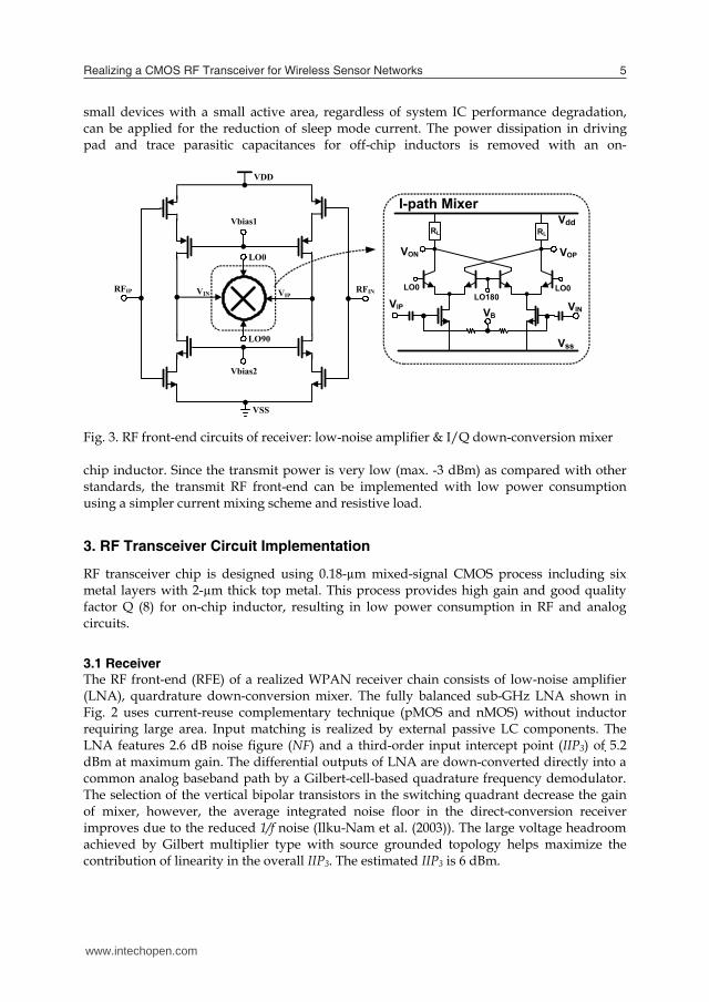
Fig. 3. RF front-end circuits of receiver: low-noise amplifier & I/Q down-conversion mixer chip inductor. Since the transmit power is very low (max. -3 dBm) as compared with other standards, the transmit RF front-end can be implemented with low power consumption using a simpler current mixing scheme and resistive load.
3. RF Transceiver Circuit Implementation
RF transceiver chip is designed using 0.18-µm mixed-signal CMOS process including six metal layers with 2-µm thick top metal. This process provides high gain and good quality factor Q (8) for on-chip inductor, resulting in low power consumption in RF and analog circuits.
3.1 Receiver The RF front-end (RFE) of a realized WPAN receiver chain consists of low-noise amplifier (LNA), quardrature down-conversion mixer. The fully balanced sub-GHz LNA shown in Fig. 2 uses current-reuse complementary technique (pMOS and nMOS) without inductor requiring large area. Input matching is realized by external passive LC components. The LNA features 2.6 dB noise figure (NF) and a third-order input intercept point (IIP3) of 5.2 dBm at maximum gain. The differential outputs of LNA are down-converted directly into a common analog baseband path by a Gilbert-cell-based quadrature frequency demodulator. The selection of the vertical bipolar transistors in the switching quadrant decrease the gain of mixer, however, the average integrated noise floor in the direct-conversion receiver improves due to the reduced 1/f noise (Ilku-Nam et al. (2003)). The large voltage headroom achieved by Gilbert multiplier type with source grounded topology helps maximize the contribution of linearity in the overall IIP3. The estimated IIP3 is 6 dBm.
VIN
VDD
VSS
Vbias1
Vbias2
RFIP RFINVIP
LO0
LO90
VIPLO180
LO0LO0
VddRL RL
Vss
VON VOP
VBVIN
I-path Mixer
www.intechopen.com
Realizing a CMOS RF Transceiver for Wireless Sensor Networks 5
Fig. 2. Overall system architecture supporting wireless sensor networks in sub-GHz ISM-band: RF transceiver & Baseband Processor and then down-converted to zero-IF I/Q signals by two identical mixers driven by quadrature LO signals from a frequency synthesizer. At the analog baseband stage, using a third-order RC filter and programmable gain amplifier simultaneously performs channel selection filtering, signal amplification, and dc-offset cancellation. In addition, I/Q 4-bit dual flash-ADCs are connected to interface of MODEM block. The transmitter adopts a zero-IF modulation with up-conversion mixer using a current mixing scheme. Baseband BPSK signals generated by digital modulator in MODEM block are followed by a 6-bit DAC. A mixer does directly up-convert the baseband signals directly 900-MHz, which is combined by RC low-pass filter. Since BPSK modulation is a constant envelop modulation, a nonlinear power amplifier with high efficiency can be used for high power emission. For generating 900-MHz LO signals with 2-MHz channel spacing, an integer-N frequency synthesizer derived from a 30-MHz crystal oscillator with 30-ppm accuracy is implemented. A 1.8GHz LO signals are generated by a VCO with a small area and high Q (quality factor) on-chip inductor. A divide-by-two circuit then produces the 900-MHz LO I/Q signals for frequency mixing of TX and RX mode. The frequency synthesizer is implemented in fully differential type, for immunity to common mode noise. In consideration of RF transceiver IC implementation for WSN applications, the low power consumption is a key issue. To achieve this, adequate trade-offs are required for system power consumption, chip area, gain, noise figure, and linearity. Since the radio will operate with a very low-duty cycle for WSN applications, the sleep mode current and battery leakage current can be reduced with the optimization of current sources. Also, the use of
Power AMP
Ant.
LNA
I-DownMix
Q-DownMix
4bitADC
RSSI
T/RSW BPF
Frequency Synthsizer
DividersBaseband/MAC
(Modem,Processor)
6bitDAC
RF Modulated Signal
LPF / PGAI/Q offset rej.
DC- Correct & LPF
RF Transceiver
Xtal
RXIdata[0:3]
RXQdata[0:3]
TXdata[0:5]
VCO[1.8GHz]
Serial interfacecontrol
SPILogic
small devices with a small active area, regardless of system IC performance degradation, can be applied for the reduction of sleep mode current. The power dissipation in driving pad and trace parasitic capacitances for off-chip inductors is removed with an on-
Fig. 3. RF front-end circuits of receiver: low-noise amplifier & I/Q down-conversion mixer chip inductor. Since the transmit power is very low (max. -3 dBm) as compared with other standards, the transmit RF front-end can be implemented with low power consumption using a simpler current mixing scheme and resistive load.
3. RF Transceiver Circuit Implementation
RF transceiver chip is designed using 0.18-µm mixed-signal CMOS process including six metal layers with 2-µm thick top metal. This process provides high gain and good quality factor Q (8) for on-chip inductor, resulting in low power consumption in RF and analog circuits.
3.1 Receiver The RF front-end (RFE) of a realized WPAN receiver chain consists of low-noise amplifier (LNA), quardrature down-conversion mixer. The fully balanced sub-GHz LNA shown in Fig. 2 uses current-reuse complementary technique (pMOS and nMOS) without inductor requiring large area. Input matching is realized by external passive LC components. The LNA features 2.6 dB noise figure (NF) and a third-order input intercept point (IIP3) of 5.2 dBm at maximum gain. The differential outputs of LNA are down-converted directly into a common analog baseband path by a Gilbert-cell-based quadrature frequency demodulator. The selection of the vertical bipolar transistors in the switching quadrant decrease the gain of mixer, however, the average integrated noise floor in the direct-conversion receiver improves due to the reduced 1/f noise (Ilku-Nam et al. (2003)). The large voltage headroom achieved by Gilbert multiplier type with source grounded topology helps maximize the contribution of linearity in the overall IIP3. The estimated IIP3 is 6 dBm.
VIN
VDD
VSS
Vbias1
Vbias2
RFIP RFINVIP
LO0
LO90
VIPLO180
LO0LO0
VddRL RL
Vss
VON VOP
VBVIN
I-path Mixer
www.intechopen.com
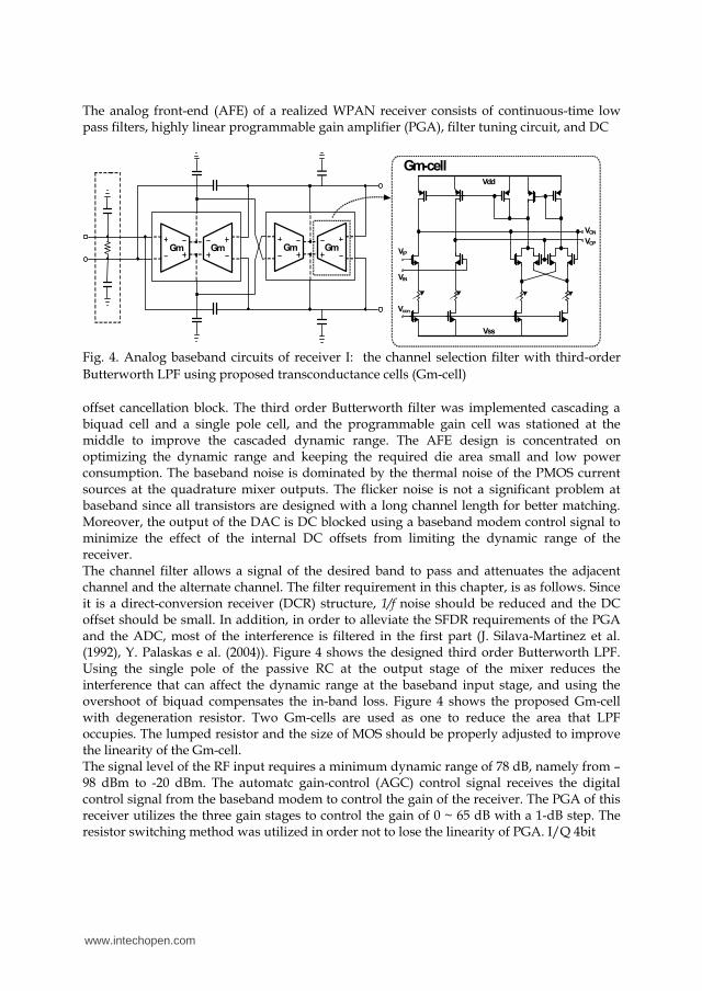
The analog front-end (AFE) of a realized WPAN receiver consists of continuous-time low pass filters, highly linear programmable gain amplifier (PGA), filter tuning circuit, and DC
Gm Gm Gm Gm VIP
Vcon
VIN
Vdd
Vss
VOP
VON
Gm-cell
Fig. 4. Analog baseband circuits of receiver I: the channel selection filter with third-order Butterworth LPF using proposed transconductance cells (Gm-cell) offset cancellation block. The third order Butterworth filter was implemented cascading a biquad cell and a single pole cell, and the programmable gain cell was stationed at the middle to improve the cascaded dynamic range. The AFE design is concentrated on optimizing the dynamic range and keeping the required die area small and low power consumption. The baseband noise is dominated by the thermal noise of the PMOS current sources at the quadrature mixer outputs. The flicker noise is not a significant problem at baseband since all transistors are designed with a long channel length for better matching. Moreover, the output of the DAC is DC blocked using a baseband modem control signal to minimize the effect of the internal DC offsets from limiting the dynamic range of the receiver. The channel filter allows a signal of the desired band to pass and attenuates the adjacent channel and the alternate channel. The filter requirement in this chapter, is as follows. Since it is a direct-conversion receiver (DCR) structure, 1/f noise should be reduced and the DC offset should be small. In addition, in order to alleviate the SFDR requirements of the PGA and the ADC, most of the interference is filtered in the first part (J. Silava-Martinez et al. (1992), Y. Palaskas e al. (2004)). Figure 4 shows the designed third order Butterworth LPF. Using the single pole of the passive RC at the output stage of the mixer reduces the interference that can affect the dynamic range at the baseband input stage, and using the overshoot of biquad compensates the in-band loss. Figure 4 shows the proposed Gm-cell with degeneration resistor. Two Gm-cells are used as one to reduce the area that LPF occupies. The lumped resistor and the size of MOS should be properly adjusted to improve the linearity of the Gm-cell. The signal level of the RF input requires a minimum dynamic range of 78 dB, namely from – 98 dBm to -20 dBm. The automatc gain-control (AGC) control signal receives the digital control signal from the baseband modem to control the gain of the receiver. The PGA of this receiver utilizes the three gain stages to control the gain of 0 ~ 65 dB with a 1-dB step. The resistor switching method was utilized in order not to lose the linearity of PGA. I/Q 4bit
Fig. 5. Analog baseband circuits of receiver II: (a) The tuning circuit for channel selection filter, (b) The circuit of a fusing cell for filter-tuning, (c) DAC schematic for DC offset adjustment dual flash-ADCs are designed for interface of baseband modem block. The simulated maximum DC current consumption of an overall receiver path is 6 mA. Figure 5 shows the automatic-tuning circuit, which is based on indirect tuning method. Since the characteristics of the Gm-C filter are determined by the transconductance value, the gm has to be controlled to keep a fixed pole frequency. The gm value should not be changed even by process variations or outer environment changes. As shown in Fig. 5(a), it is important to keep a gm value and a ratio of gm output current to gm input voltage equal. And the required current for sinking or sourcing is designed to minimize changes of gm by reducing current change due to the temperature variation from bias block. The current I1 in Fig. 5(a) offsets the MOS of the bias part as well as the temperature variation of resistance so as to minimize the changes of voltage Vab due to the temperature and to evenly maintain the input voltage of the gm-cell. The converging time of tuning circuit is designed to less than 100 msec. If the cut-off frequency differs from the designed value, as a parameter set up the first time it distorts the value of gm by the process variations, gm should be adjusted by changing current I2 by fusing. Fusing is controlled by serial port
4
Fusing Point
Zenb
dinb
PoR
do
I
M1
a
VcmR
R
I1
I1
Gm
C
CI2
I2
Vref1
Vref2
Up/DnCnt
Comparator
a
b
(a) (b)
d7
d0b
d1b
d2b
d3b
d4b
d5b
d6b
d0b
d7
d1b
d2b
d3b
d4b
d5b
d6b
d7b
d7b
VcmR
R
Iref Vinp
VinnM1
M2 M3M4 M5
P1 P2 P3 P4 P5
(c)
www.intechopen.com

Realizing a CMOS RF Transceiver for Wireless Sensor Networks 7
The analog front-end (AFE) of a realized WPAN receiver consists of continuous-time low pass filters, highly linear programmable gain amplifier (PGA), filter tuning circuit, and DC
Gm Gm Gm Gm VIP
Vcon
VIN
Vdd
Vss
VOP
VON
Gm-cell
Fig. 4. Analog baseband circuits of receiver I: the channel selection filter with third-order Butterworth LPF using proposed transconductance cells (Gm-cell) offset cancellation block. The third order Butterworth filter was implemented cascading a biquad cell and a single pole cell, and the programmable gain cell was stationed at the middle to improve the cascaded dynamic range. The AFE design is concentrated on optimizing the dynamic range and keeping the required die area small and low power consumption. The baseband noise is dominated by the thermal noise of the PMOS current sources at the quadrature mixer outputs. The flicker noise is not a significant problem at baseband since all transistors are designed with a long channel length for better matching. Moreover, the output of the DAC is DC blocked using a baseband modem control signal to minimize the effect of the internal DC offsets from limiting the dynamic range of the receiver. The channel filter allows a signal of the desired band to pass and attenuates the adjacent channel and the alternate channel. The filter requirement in this chapter, is as follows. Since it is a direct-conversion receiver (DCR) structure, 1/f noise should be reduced and the DC offset should be small. In addition, in order to alleviate the SFDR requirements of the PGA and the ADC, most of the interference is filtered in the first part (J. Silava-Martinez et al. (1992), Y. Palaskas e al. (2004)). Figure 4 shows the designed third order Butterworth LPF. Using the single pole of the passive RC at the output stage of the mixer reduces the interference that can affect the dynamic range at the baseband input stage, and using the overshoot of biquad compensates the in-band loss. Figure 4 shows the proposed Gm-cell with degeneration resistor. Two Gm-cells are used as one to reduce the area that LPF occupies. The lumped resistor and the size of MOS should be properly adjusted to improve the linearity of the Gm-cell. The signal level of the RF input requires a minimum dynamic range of 78 dB, namely from – 98 dBm to -20 dBm. The automatc gain-control (AGC) control signal receives the digital control signal from the baseband modem to control the gain of the receiver. The PGA of this receiver utilizes the three gain stages to control the gain of 0 ~ 65 dB with a 1-dB step. The resistor switching method was utilized in order not to lose the linearity of PGA. I/Q 4bit
Fig. 5. Analog baseband circuits of receiver II: (a) The tuning circuit for channel selection filter, (b) The circuit of a fusing cell for filter-tuning, (c) DAC schematic for DC offset adjustment dual flash-ADCs are designed for interface of baseband modem block. The simulated maximum DC current consumption of an overall receiver path is 6 mA. Figure 5 shows the automatic-tuning circuit, which is based on indirect tuning method. Since the characteristics of the Gm-C filter are determined by the transconductance value, the gm has to be controlled to keep a fixed pole frequency. The gm value should not be changed even by process variations or outer environment changes. As shown in Fig. 5(a), it is important to keep a gm value and a ratio of gm output current to gm input voltage equal. And the required current for sinking or sourcing is designed to minimize changes of gm by reducing current change due to the temperature variation from bias block. The current I1 in Fig. 5(a) offsets the MOS of the bias part as well as the temperature variation of resistance so as to minimize the changes of voltage Vab due to the temperature and to evenly maintain the input voltage of the gm-cell. The converging time of tuning circuit is designed to less than 100 msec. If the cut-off frequency differs from the designed value, as a parameter set up the first time it distorts the value of gm by the process variations, gm should be adjusted by changing current I2 by fusing. Fusing is controlled by serial port
4
Fusing Point
Zenb
dinb
PoR
do
I
M1
a
VcmR
R
I1
I1
Gm
C
CI2
I2
Vref1
Vref2
Up/DnCnt
Comparator
a
b
(a) (b)
d7
d0b
d1b
d2b
d3b
d4b
d5b
d6b
d0b
d7
d1b
d2b
d3b
d4b
d5b
d6b
d7b
d7b
VcmR
R
Iref Vinp
VinnM1
M2 M3M4 M5
P1 P2 P3 P4 P5
(c)
www.intechopen.com

Fig. 6. Transmitter circuits: (a) Up-conversion I/Q-modulator using current-mixing scheme (b) Drive-amplifier with off-chip inductor interface (SPI), and there is no change in value once it is put in. Figure 5(b) represents the circuit diagram of fusing cell. The fusing cell is a circuit which amplifies the voltage, which is set in ratio of PMOS channel resistance to NMOS channel resistance within the range of power on reset (‘Low’ PoR signal) at power-on. To inverting amplifier, the signal is latched and displays the latched value without change while normal operation (‘High’ PoR signal). The ‘Zenb’ is a signal of ‘fusing enable’, ‘dinb’ is a ‘data input signal’ controllable via SPI. The ‘PoR’ is a signal for ‘enable’ at the mode of ‘power on reset’, while ‘do’ is an output signal of fusing cell. Once the fusing signal turns to ‘enable’, the output signal of fusing cell is fixed regardless of the data input signal. The current capacity of M1 should have more than 1 mA in order to disconnect the node of a fusing point at transmitting the fusing enable signal. For DC offset adjustment, it is important for the cancellation of DC-offsets generated at the back side of PGA1 and to use the feedback loop to reduce the offset at the LPF output. Figure 5(c) shows the DAC to convert the 8-bit data into the input voltage of the PGA. The resolution for 1 bit is 5 mV, and the DC offset change at the LPF output is ±640 mV. The size of MOS (P1~P5, M1~M5) used, as a current mirror of the DAC circuit has to be appropriate in consideration of the current mismatch. The aspect ratio of the MOS is used by 20μm/2μm.
3.2 Transmitter In the transmitter path, the BPSK modulated baseband signal is converted from digital to analog before being applied to frequency up-translation block. Fig.6 (a) shows the schematic of up-conversion mixer with RC low-pass filter. The baseband analog signal is filtered by second RC low-pass filter, and then is translated into RF frequency by up-conversion
VINVIP
LO180LO0
ISS/2
LO0
Cf
ISS/2
RdRf Rd Rf
VDDRL RL
VSS
VON VOP
Pon
VDD
VSS
Pop
Vbias
Pip Pin
Loff chip
On ChipLdown bond
(a) (b)
modulator with balanced Gilbert-cell using current-mixing scheme. The major advantage of current mixing relaxes a requirement of heavy linearity of modulator inputs from high Fig. 7. Frequency synthesizer block-diagram with LC voltage-controlled oscillator voltage-driving DAC output signal. In addition, this scheme for frequency-up modulation can produce satisfactory results for high modulation quality, low-power consumption, and good linearity. This balanced mixer converts baseband signal directly up to 900 MHz and deliver -20 dBm differential signal to power amplifier. LO emission is due to differential mismatch in the modulator circuit, while spectrum re-growth is due to LO (0/90-degree) quardrature imbalance and nonlinearity of the Gilbert-cell. Layout is fulfilled very carefully to maintain symmetry for differential and quardrature signals, which minimizes both LO emission and spectrum re-growth. Fig.6 (b) shows the driver amplifier of a differential common source topology with off-chip inductor having a high Q. The multiple down-bond wire inductors are applied for the minimization of spectrum re-growth. The simulated DC current consumption of an overall transmitter path is 7 mA.
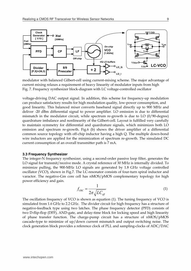
3.3 Frequency Synthesizer The integer-N frequency synthesizer, using a second-order passive loop filter, generates the LO signal for transmit/receive mode. A crystal reference of 30 MHz is internally divided. To minimize pulling, the 900-MHz LO signals are generated by 1.8 GHz voltage controlled oscillator (VCO), shown in Fig.7. The LC-resonator consists of four-turn spiral inductor and varactor. The negative-Gm core cell has nMOS/pMOS complementary topology for high power efficiency and gain.
12OSC
eff
fLC (1)
The oscillation frequency of VCO is shown as equation (1). The tuning frequency of VCO is simulated from 1.6 GHz to 2.2 GHz. The divider circuit for high frequency has a structure of negative-feedback type using two latches. The phase frequency detector (PFD) consists of two D-flip-flop (DFF), AND-gate, and delay-time block for locking speed and high linearity of phase transfer function. The charge-pump circuit has a structure of nMOS/pMOS cascade-type to minimize of up/down current mismatch and output switching noise. The clock generation block provides a reference clock of PLL and sampling-clocks of ADC/DAC
PFD CP LF
ClockGenerator
[ 1/15 ]Xtal[30MHz]
[2MHz]Fref.
[1.8GHz]VCO
Off-chip
÷ 2Divider[P,S]=(56,5)
8/9Prescaler
I/Q LO buffers
LO_I
LO_Q
Vop Von
VDD
VSSVbias
Vc
LC-VCO
On-chip
www.intechopen.com
Realizing a CMOS RF Transceiver for Wireless Sensor Networks 9
Fig. 6. Transmitter circuits: (a) Up-conversion I/Q-modulator using current-mixing scheme (b) Drive-amplifier with off-chip inductor interface (SPI), and there is no change in value once it is put in. Figure 5(b) represents the circuit diagram of fusing cell. The fusing cell is a circuit which amplifies the voltage, which is set in ratio of PMOS channel resistance to NMOS channel resistance within the range of power on reset (‘Low’ PoR signal) at power-on. To inverting amplifier, the signal is latched and displays the latched value without change while normal operation (‘High’ PoR signal). The ‘Zenb’ is a signal of ‘fusing enable’, ‘dinb’ is a ‘data input signal’ controllable via SPI. The ‘PoR’ is a signal for ‘enable’ at the mode of ‘power on reset’, while ‘do’ is an output signal of fusing cell. Once the fusing signal turns to ‘enable’, the output signal of fusing cell is fixed regardless of the data input signal. The current capacity of M1 should have more than 1 mA in order to disconnect the node of a fusing point at transmitting the fusing enable signal. For DC offset adjustment, it is important for the cancellation of DC-offsets generated at the back side of PGA1 and to use the feedback loop to reduce the offset at the LPF output. Figure 5(c) shows the DAC to convert the 8-bit data into the input voltage of the PGA. The resolution for 1 bit is 5 mV, and the DC offset change at the LPF output is ±640 mV. The size of MOS (P1~P5, M1~M5) used, as a current mirror of the DAC circuit has to be appropriate in consideration of the current mismatch. The aspect ratio of the MOS is used by 20μm/2μm.
3.2 Transmitter In the transmitter path, the BPSK modulated baseband signal is converted from digital to analog before being applied to frequency up-translation block. Fig.6 (a) shows the schematic of up-conversion mixer with RC low-pass filter. The baseband analog signal is filtered by second RC low-pass filter, and then is translated into RF frequency by up-conversion
VINVIP
LO180LO0
ISS/2
LO0
Cf
ISS/2
RdRf Rd Rf
VDDRL RL
VSS
VON VOP
Pon
VDD
VSS
Pop
Vbias
Pip Pin
Loff chip
On ChipLdown bond
(a) (b)
modulator with balanced Gilbert-cell using current-mixing scheme. The major advantage of current mixing relaxes a requirement of heavy linearity of modulator inputs from high Fig. 7. Frequency synthesizer block-diagram with LC voltage-controlled oscillator voltage-driving DAC output signal. In addition, this scheme for frequency-up modulation can produce satisfactory results for high modulation quality, low-power consumption, and good linearity. This balanced mixer converts baseband signal directly up to 900 MHz and deliver -20 dBm differential signal to power amplifier. LO emission is due to differential mismatch in the modulator circuit, while spectrum re-growth is due to LO (0/90-degree) quardrature imbalance and nonlinearity of the Gilbert-cell. Layout is fulfilled very carefully to maintain symmetry for differential and quardrature signals, which minimizes both LO emission and spectrum re-growth. Fig.6 (b) shows the driver amplifier of a differential common source topology with off-chip inductor having a high Q. The multiple down-bond wire inductors are applied for the minimization of spectrum re-growth. The simulated DC current consumption of an overall transmitter path is 7 mA.
3.3 Frequency Synthesizer The integer-N frequency synthesizer, using a second-order passive loop filter, generates the LO signal for transmit/receive mode. A crystal reference of 30 MHz is internally divided. To minimize pulling, the 900-MHz LO signals are generated by 1.8 GHz voltage controlled oscillator (VCO), shown in Fig.7. The LC-resonator consists of four-turn spiral inductor and varactor. The negative-Gm core cell has nMOS/pMOS complementary topology for high power efficiency and gain.
12OSC
eff
fLC (1)
The oscillation frequency of VCO is shown as equation (1). The tuning frequency of VCO is simulated from 1.6 GHz to 2.2 GHz. The divider circuit for high frequency has a structure of negative-feedback type using two latches. The phase frequency detector (PFD) consists of two D-flip-flop (DFF), AND-gate, and delay-time block for locking speed and high linearity of phase transfer function. The charge-pump circuit has a structure of nMOS/pMOS cascade-type to minimize of up/down current mismatch and output switching noise. The clock generation block provides a reference clock of PLL and sampling-clocks of ADC/DAC
PFD CP LF
ClockGenerator
[ 1/15 ]Xtal[30MHz]
[2MHz]Fref.
[1.8GHz]VCO
Off-chip
÷ 2Divider[P,S]=(56,5)
8/9Prescaler
I/Q LO buffers
LO_I
LO_Q
Vop Von
VDD
VSSVbias
Vc
LC-VCO
On-chip
www.intechopen.com

using an external 30-MHz crystal-oscillator. The simulated DC current consumption of an overall frequency synthesizer path is 8 mA. Fig. 9. Measured results: (a) cascaded noise figure (NF), (b) cascaded IIP3 of overall receiver
4. Measured Results
Fig. 10. Measured result of spectrum mask of transmitter
SPI
RX
PLL
TX
Fig. 8. Die microphotograph
Frequency [MHz]905 910 915 920 925
NF
[dB
]
8.0
8.5
9.0
9.5
10.0
10.5
11.0
RF Input Power [dBm]
-60 -50 -40 -30 -20 -10 0
Out
put P
ower
[dBm
]
-60
-40
-20
0 IIP3
(a) (b)
Fig. 11. Measured result of vector signal analysis of transmitter
A radio transceiver die microphotograph, which consists of transmitter, receiver, and frequency synthesizer with on-chip VCO, is shown in Fig. 8. The total die area is 1.8 2.2-mm2 and it consumes only 29 mW in the transmit-mode, 25-mW in the receive-mode and a LPCC48 package is used. The overall receiver features a cascaded-NF of 9.5 dB for 900 MHz band as shown in Fig. 9(a). Overall receive cascaded- IIP3 as shown in Fig. 9(b) is -10 dBm and the maximum gain of receiver is 88dB. The automatic gain control (AGC) of receiver is 86dB with 1dB step and selectivity is -48 dBc at 5 MHz offset frequency. The 40 kHz baseband single signal is up-converted by 906 MHz RF carrier signal and wanted-signals are 25dB higher than third-order harmonics. The spectrum density at the output of transmitter satisfies the required spectrum mask as shown in Fig. 10, which is above 28 dBc at the ±1.2-MHz offset frequency. Due to the low in-band integrated phase noise and the digital calibration that eliminates I/Q mismatch and baseband filter mismatch, transmitter EVM is dominated by nonlinearities (Behzad Razzavi (1997), I. Vassiliou et al. (2003), K. Vavelidis et al. (2004)). As shown in Fig. 11, a reference design achieves 6.3 % EVM for an output power
(a)
www.intechopen.com

Realizing a CMOS RF Transceiver for Wireless Sensor Networks 11
using an external 30-MHz crystal-oscillator. The simulated DC current consumption of an overall frequency synthesizer path is 8 mA. Fig. 9. Measured results: (a) cascaded noise figure (NF), (b) cascaded IIP3 of overall receiver
4. Measured Results
Fig. 10. Measured result of spectrum mask of transmitter
SPI
RX
PLL
TX
Fig. 8. Die microphotograph
Frequency [MHz]905 910 915 920 925
NF
[dB
]
8.0
8.5
9.0
9.5
10.0
10.5
11.0
RF Input Power [dBm]
-60 -50 -40 -30 -20 -10 0
Out
put P
ower
[dBm
]
-60
-40
-20
0 IIP3
(a) (b)
Fig. 11. Measured result of vector signal analysis of transmitter
A radio transceiver die microphotograph, which consists of transmitter, receiver, and frequency synthesizer with on-chip VCO, is shown in Fig. 8. The total die area is 1.8 2.2-mm2 and it consumes only 29 mW in the transmit-mode, 25-mW in the receive-mode and a LPCC48 package is used. The overall receiver features a cascaded-NF of 9.5 dB for 900 MHz band as shown in Fig. 9(a). Overall receive cascaded- IIP3 as shown in Fig. 9(b) is -10 dBm and the maximum gain of receiver is 88dB. The automatic gain control (AGC) of receiver is 86dB with 1dB step and selectivity is -48 dBc at 5 MHz offset frequency. The 40 kHz baseband single signal is up-converted by 906 MHz RF carrier signal and wanted-signals are 25dB higher than third-order harmonics. The spectrum density at the output of transmitter satisfies the required spectrum mask as shown in Fig. 10, which is above 28 dBc at the ±1.2-MHz offset frequency. Due to the low in-band integrated phase noise and the digital calibration that eliminates I/Q mismatch and baseband filter mismatch, transmitter EVM is dominated by nonlinearities (Behzad Razzavi (1997), I. Vassiliou et al. (2003), K. Vavelidis et al. (2004)). As shown in Fig. 11, a reference design achieves 6.3 % EVM for an output power
(a)
www.intechopen.com

Frequency offset100 Hz 1 MHz100 kHz10 kHz1 kHz
-110
-90
-130
-150
(b)
Fig. 12. Measured result of phase lock loop (PLL): (a) settling time, (b) phase noise of –3dBm for sub-GHz ISM-band. Measured results of settling time and phase-noise plot of phase locked loop (PLL) are shown in Fig. 12. Table 1 summarizes the UHF RF transceiver’s characteristics. The specifications of two RF transceivers (Walter Schucher et al. (2001)) and (Hiroshi Komurasaki et al. (2003)) for UHF applications are also shown for comparison in this table. The RX current is not the lowest; however, the power dissipation in RX mode is the smallest because of the 1.8 V supply voltage. Although the TX output power and RX IIP3 are a little worse due to the antenna switch and the matching network, this work has great advantages.
Specification This work Walter Schucher et al. (2001)
Hiroshi Komurasaki et al. (2003)
VDD 1.8V 2.8V 1.8V Current consum. Rx./Tx.:14/16mA Rx./Tx.: 11/20mA Rx./Tx.: 34/26mA
Die size 3.96 mm2 10 mm2 NF 9.5dB 11.8dB -76dBm IIP3 -10dBm -23.2dBm +3dBm
Max. Gain 88dB - - AGC gain range 86 - -
Selectivity -48dBc (@5MHz) - -21dBc (@4MHz) TX power +0dBm +10dBm +0dBm
EVM 6.3% - - OP1-dB +1dBm - -
LO PN. (@1MHz) -108dBc -115dBc - Table 1. The Measured Results of UHF Transceivers
5. Conclusion
A low power fully CMOS integrated RF transceiver chip for wireless sensor networks in sub-GHz ISM-band applications is implemented and measured. The IC is fabricated in 0.18-µm mixed-signal CMOS process and packaged in LPCC package. The fully monolithic transceiver consists of a receiver, a transmitter and a RF synthesizer with on-chip VCO. The overall receiver cascaded noise-figure, and cascade IIP3 are 9.5 dB, and -10 dBm,
respectively. The overall transmitter achieves less than 6.3 % error vector magnitude (EVM) for 40kbps mode. The chip uses 1.8V power supply and the current consumption is 25 mW for reception mode and 29 mW for transmission mode. This chip fully supports the IEEE 802.15.4 WPAN standard in sub-GHz mode.
6. References
Behzad Razavi (1997). Design Considerations for Direct-Conversion, IEEE Transactions on circuit and systems-II, 14, 251-260, June.
C. Cojocaru, T. Pamir, F. Balteanu, A. Namdar, D. Payer, I. Gheorghe, T. Lipan, K. Sheikh, J. Pingot, H. Paananen, M. Littow, M. Cloutier, and E. MacRobbie (2003). A 43mW Bluetooth transceiver with –91dBm sensitivity, ISSCC Dig. Tech. Papers, 90-91.
Hiroshi Komurasaki, Tomohiro Sano, Tetsuya Heima, Kazuya Yamamoto, Hideyuki Wakada, Ikuo Yasui, Masayoshi Ono, Takahiro Miki, and Naoyuki Kato (2003). A 1.8 V Operation RF CMOS Transceiver for 2.4 GHz Band GFSK Applications, IEEE Journal of Solid-State Circuit, 38, May.
IEEE Computer Society (2003). IEEE Standard for Part 15.4: Wireless Medium Access Control (MAC) and Physical Layer (PHY) specifications for Low Rate Wireless Personal Area Networks (LR-WPANs), IEEE Standard 802.15.4TM.
Ilku Nam, Young Jin Kim, and Kwyro Lee (2003). Low 1/f Noise and DC offset RF mixer for direct conversion receiver using parasitic vertical NPN bipolar transistor in deep N-well CMOS Technology, IEEE symposium on VLSI circuits digest of technical.
I. Vassiliou, K. Vavelidis, T. Georgantas, S. Plevridis, N. Haralabidis, G. Kamoulakos, C. Kapnistis, S. Kavadias, Y. Kokolakis, P. Merakos, J.C. Rudell, A. Yamanaka, S. Bouras, and I. Bouras (2003). A single-chip digitally calibrated 5.15 GHz-5.825 GHz 0.18 μm CMOS transceiver for 802.11a wireless LAN, IEEE J. Solid-State Circuits, 38, 2221–2231, December.
J. Bouras, S. Bouras, T. Georgantas, N. Haralabidis, G. Kamoulakos, C. Kapnistis, S. Kavadias, Y. Kokolakis, P. Merakos, J. Rudell, S. Plevridis, I. Vassiliou, K. Vavelidis, and A. Yamanaka (2003). A digitally calibrated 5.15– 5.825 GHz transceiver for 802.11a wireless LANS in 0.18 μm CMOS, IEEE Int. Solid-State Conf. Dig.Tech. Papers, February.
J. Silva-Martinez, M.S.J. Steyaert, and W. Sansen (1992). A 10.7 MHz, 68 dB SNR CMOS Continuous-Time Filter with On-Chip Automatic Tunig, IEEE J. Solid-State Circuits, 27, 1843-1853, December.
Kwang-Jin Koh, Mun-Yang Park, Cheon-Soo Kim, and Hyun-Kyu Yu (2004). Subharmonically Pumped CMOS Frequency Conversion (Up and Down) Circuits For 2 GHz WCDMA Direct-Conversion Transceiver, IEEE J. Solid-State Circuits, 39, 871-884, June.
K. Vavelidis, I. Vassiliou, T. Georgantas, A. Yamanaka, S. Kavadias, G. Kamoulakos, C. Kapnistis, Y. Kokolakis, A. Kyranas, P. Merakos, I. Bouras, S. Bouras, S. Plevridis, and N. Haralabidis (2004). A dual- band 5.15-5.35 GHz, 2.4-2.5 GHz 0.18 μm CMOS Transceiver for 802.11a/b/g wireless LAN, IEEE J. Solid-State Circuits, 39, 1180-1185, July.
www.intechopen.com

Realizing a CMOS RF Transceiver for Wireless Sensor Networks 13
Frequency offset100 Hz 1 MHz100 kHz10 kHz1 kHz
-110
-90
-130
-150
(b)
Fig. 12. Measured result of phase lock loop (PLL): (a) settling time, (b) phase noise of –3dBm for sub-GHz ISM-band. Measured results of settling time and phase-noise plot of phase locked loop (PLL) are shown in Fig. 12. Table 1 summarizes the UHF RF transceiver’s characteristics. The specifications of two RF transceivers (Walter Schucher et al. (2001)) and (Hiroshi Komurasaki et al. (2003)) for UHF applications are also shown for comparison in this table. The RX current is not the lowest; however, the power dissipation in RX mode is the smallest because of the 1.8 V supply voltage. Although the TX output power and RX IIP3 are a little worse due to the antenna switch and the matching network, this work has great advantages.
Specification This work Walter Schucher et al. (2001)
Hiroshi Komurasaki et al. (2003)
VDD 1.8V 2.8V 1.8V Current consum. Rx./Tx.:14/16mA Rx./Tx.: 11/20mA Rx./Tx.: 34/26mA
Die size 3.96 mm2 10 mm2 NF 9.5dB 11.8dB -76dBm IIP3 -10dBm -23.2dBm +3dBm
Max. Gain 88dB - - AGC gain range 86 - -
Selectivity -48dBc (@5MHz) - -21dBc (@4MHz) TX power +0dBm +10dBm +0dBm
EVM 6.3% - - OP1-dB +1dBm - -
LO PN. (@1MHz) -108dBc -115dBc - Table 1. The Measured Results of UHF Transceivers
5. Conclusion
A low power fully CMOS integrated RF transceiver chip for wireless sensor networks in sub-GHz ISM-band applications is implemented and measured. The IC is fabricated in 0.18-µm mixed-signal CMOS process and packaged in LPCC package. The fully monolithic transceiver consists of a receiver, a transmitter and a RF synthesizer with on-chip VCO. The overall receiver cascaded noise-figure, and cascade IIP3 are 9.5 dB, and -10 dBm,
respectively. The overall transmitter achieves less than 6.3 % error vector magnitude (EVM) for 40kbps mode. The chip uses 1.8V power supply and the current consumption is 25 mW for reception mode and 29 mW for transmission mode. This chip fully supports the IEEE 802.15.4 WPAN standard in sub-GHz mode.
6. References
Behzad Razavi (1997). Design Considerations for Direct-Conversion, IEEE Transactions on circuit and systems-II, 14, 251-260, June.
C. Cojocaru, T. Pamir, F. Balteanu, A. Namdar, D. Payer, I. Gheorghe, T. Lipan, K. Sheikh, J. Pingot, H. Paananen, M. Littow, M. Cloutier, and E. MacRobbie (2003). A 43mW Bluetooth transceiver with –91dBm sensitivity, ISSCC Dig. Tech. Papers, 90-91.
Hiroshi Komurasaki, Tomohiro Sano, Tetsuya Heima, Kazuya Yamamoto, Hideyuki Wakada, Ikuo Yasui, Masayoshi Ono, Takahiro Miki, and Naoyuki Kato (2003). A 1.8 V Operation RF CMOS Transceiver for 2.4 GHz Band GFSK Applications, IEEE Journal of Solid-State Circuit, 38, May.
IEEE Computer Society (2003). IEEE Standard for Part 15.4: Wireless Medium Access Control (MAC) and Physical Layer (PHY) specifications for Low Rate Wireless Personal Area Networks (LR-WPANs), IEEE Standard 802.15.4TM.
Ilku Nam, Young Jin Kim, and Kwyro Lee (2003). Low 1/f Noise and DC offset RF mixer for direct conversion receiver using parasitic vertical NPN bipolar transistor in deep N-well CMOS Technology, IEEE symposium on VLSI circuits digest of technical.
I. Vassiliou, K. Vavelidis, T. Georgantas, S. Plevridis, N. Haralabidis, G. Kamoulakos, C. Kapnistis, S. Kavadias, Y. Kokolakis, P. Merakos, J.C. Rudell, A. Yamanaka, S. Bouras, and I. Bouras (2003). A single-chip digitally calibrated 5.15 GHz-5.825 GHz 0.18 μm CMOS transceiver for 802.11a wireless LAN, IEEE J. Solid-State Circuits, 38, 2221–2231, December.
J. Bouras, S. Bouras, T. Georgantas, N. Haralabidis, G. Kamoulakos, C. Kapnistis, S. Kavadias, Y. Kokolakis, P. Merakos, J. Rudell, S. Plevridis, I. Vassiliou, K. Vavelidis, and A. Yamanaka (2003). A digitally calibrated 5.15– 5.825 GHz transceiver for 802.11a wireless LANS in 0.18 μm CMOS, IEEE Int. Solid-State Conf. Dig.Tech. Papers, February.
J. Silva-Martinez, M.S.J. Steyaert, and W. Sansen (1992). A 10.7 MHz, 68 dB SNR CMOS Continuous-Time Filter with On-Chip Automatic Tunig, IEEE J. Solid-State Circuits, 27, 1843-1853, December.
Kwang-Jin Koh, Mun-Yang Park, Cheon-Soo Kim, and Hyun-Kyu Yu (2004). Subharmonically Pumped CMOS Frequency Conversion (Up and Down) Circuits For 2 GHz WCDMA Direct-Conversion Transceiver, IEEE J. Solid-State Circuits, 39, 871-884, June.
K. Vavelidis, I. Vassiliou, T. Georgantas, A. Yamanaka, S. Kavadias, G. Kamoulakos, C. Kapnistis, Y. Kokolakis, A. Kyranas, P. Merakos, I. Bouras, S. Bouras, S. Plevridis, and N. Haralabidis (2004). A dual- band 5.15-5.35 GHz, 2.4-2.5 GHz 0.18 μm CMOS Transceiver for 802.11a/b/g wireless LAN, IEEE J. Solid-State Circuits, 39, 1180-1185, July.
www.intechopen.com

M. Zargari, M. Terrovitis, S.H.M. Jen, B.J. Kaczynski, MeeLan Lee, M.P. Mack, S.S. Mehta, S. Mendis, K. Onodera, H. Samavati, W.W. Si, K. Singh, A. Tabatabaei, D. Weber, D.K. Su, and B.A. Wooley (2004). A Single-Chip Dual-Band Tri-Mode CMOS Transceiver for IEEE 802.11a/b/g Wireless LAN”, IEEE J. Solid-State Circuits, 39, 2239-2249, December.
M. Valla, G. Montagna, R. Castello, R. Tonietto, and I. Bietti (2005). A 72 mW CMOS 802.11a Direct Conversion Front-End with 3.5 dB NF and 200 kHz 1/f Noise Corner, IEEE J. Solid-State Circuits, 40, 970-977, April.
Pengfei Zhang, T. Nguyen, C. Lam, D. Gambetta, T. Soorapanth, Baohong Cheng, S. Hart, I. Sever, T. Bourdi, A. Tham, and B. Razavi (2003). “A 5 GHz Direct-Conversion CMOS Transceiver” IEEE Journal of Solid-State Circuit, 38, December.
P. S. Choi, H. C. Park, S. Y. Kim, S. C. Park, I. K. Nam, T. W. Kim, S. J. Park, S. H. Shin, M. S. Kim, K. C. Kang, Y. W. Ku; H. J. Choi, S. M. Park, and K. R. Lee (2003). “An Experimental Coin-Sized Radio for Extremely Low-Power WPAN Application at 2.4GHz,” IEEE J. Solid-State Circuits, 12, 2258-2268, December.
S.F.R. Chang, Wen-Lin Chen, Shuen-Chien Chang, Chi-Kang Tu, Chang-Lin Wei, Chih-Hung Chien, Cheng-Hua Tsai, J. Chen, and A. Chen (2005), A Dual-Band RF Transceiver for Multistandard WLAN Applications. IEEE Transaction on Microwave Theory and Techniques, 53, 1040-1055, March.
S. Sarkar, P. Sen, A. Raghavan, S. Chakarborty, and J. Laskar (2003). Development of 2.4 GHz RF Transceiver Front-end Chipset in 0.25µm CMOS, Proceedings of the 16th International Conference on VLSI Design.
Walter Schuchter, Guenter Krasser, and Guenter Hofer (2001). A Single Chip FSK/ASK 900MHz Transceiver in a Standard 0.25um CMOS Technology, IEEE RFIC Symposium.
W. Hioe, K. Maio, T. Oshima, Y. Shibahara, T. Doi, K. Ozaki, and S. Arayashiki, “0.18-um CMOS Bluetooth Analog Receiver With 88-dBm Sensitivity (2004). IEEE J. Solid-State Circuits, 39, 374-377, February.
Y. J. Jung, H. S. Jeong, E. S. Song, J. H. Lee, S. W. Lee, D. Y. Seo, I. H. Song, S. H. Jung, J. B. Park, D. K. Jeong, S. I. Chae, and W. Kim (2004). A 2.4-GHz 0.25um CMOS dual-mode direct-conversion transceiver for bluetooth and 802.11b, IEEE Journal of solid-state circuits, 39, July..
Y. K. Park, H. M. Seo, Y. K. Moon, K. H. Won, and S. D. Kim (2005). Low Power Radio Receiver Specifications of Ubiquitous System for Coexistence with Various Wireless Devices in 2.4GHz ISM-band, The 20th International Technical Conference on Circuits/System, Computers and Communications, July.
Y. Palaskas, Y. Tsividis, V. Prodanov, and V. Boccuzzi (2004). A Divide and Conquer Technique for Implementing Wide Dynamic Range Continuous-Time Filters, IEEE J. Solid-State Circuits, 39, 297-307, February.
www.intechopen.com

Wireless Sensor NetworksEdited by
ISBN 978-953-307-325-5Hard cover, 342 pagesPublisher InTechPublished online 29, June, 2011Published in print edition June, 2011
InTech EuropeUniversity Campus STeP Ri Slavka Krautzeka 83/A 51000 Rijeka, Croatia Phone: +385 (51) 770 447 Fax: +385 (51) 686 166www.intechopen.com
InTech ChinaUnit 405, Office Block, Hotel Equatorial Shanghai No.65, Yan An Road (West), Shanghai, 200040, China
Phone: +86-21-62489820 Fax: +86-21-62489821
How to referenceIn order to correctly reference this scholarly work, feel free to copy and paste the following:
Hae-Moon Seo (2011). Realizing a CMOS RF Transceiver for Wireless Sensor Networks, Wireless SensorNetworks, (Ed.), ISBN: 978-953-307-325-5, InTech, Available from:http://www.intechopen.com/books/wireless-sensor-networks/realizing-a-cmos-rf-transceiver-for-wireless-sensor-networks

© 2011 The Author(s). Licensee IntechOpen. This chapter is distributedunder the terms of the Creative Commons Attribution-NonCommercial-ShareAlike-3.0 License, which permits use, distribution and reproduction fornon-commercial purposes, provided the original is properly cited andderivative works building on this content are distributed under the samelicense.