guidelines for reticle data management ver.2.0 (english ... · pdf filesub-committee on...
TRANSCRIPT

1
Guidelines for Reticle Data Management Ver.2.0(English Version)
JEITA (Japan Electronics and Information Technology Industries Association)Committee on Semiconductor Production EngineeringSub-committee on Reticle Management System
Sub-committee MembersMichio Honma (NECEL)NEC Electronics CorporationCorporate Strategic Planning Unit
Nobuyuki Iriki (Renesas)RENESAS Technology Co.LSI Manufacturing UnitWafer Process Engineering Development Div.
Takashi Satoh (Toshiba)TOSHIBA CORPORATIONProcess & Manufacturing Engineering CenterAdvanced ULSI Engineering Dept.II
Norihiko Miyazaki (Fujitsu)FUJITSU LIMITED Semiconductor GroupManufacturing Technology Development Div.MASK Technology Dept.
Toshio Onodera (Oki)Oki Electric Industry Co., Ltd.Silicon Manufacturing Company (SiMC)WP Business Div.WP Business Dept.
Toshiharu Matsuda (SANYO)SANYO Electric Co.,Ltd.Semiconductor CompanyLSI BUEngineering Dept.
Tamotsu Uga (ROHM)ROHM Co.,Ltd.MASK Production Dept.VLSI Operation Div.
ObserversSEMI Japan Reticle Data Management TF: Hidehiro Higashino (Oki)
Selete: Iwao Higashikawa , Nobuyuki Yoshioka
Oki Electric Industry Co., Ltd.Silicon Manufacturing Company (SiMC)WP Business Div.WP Business Dept.
Semiconductor Leading Edge Technologies Inc.Advanced Technology Dept.

2
Contents
1. Introduction 1.1 Preface 1.2 The overview of Ver11.3 Background from Ver1 to Ver21.4 Purpose of Ver21.5 Scope 1.6 Standardization objects and definition1.7 Relationship with the related standardization requirement
2. General guideline 2.1 Sharing of reticle data2.2 The standardized expression for usability of pattern data
3. Guideline for application 3.1 Creative association among applications that use design information 3.2 Comprehensive reusability in process module optimization3.3 Strengthening linkage between design and manufacturing3.4 The prospect through the process (extension from a design to a back process)
4. The model of Global Joint Guidance

3
1. Introduction
1.1 Preface
Our semiconductor business has experienced the period of severe depression when market shrank and there was severe competition. Now we are getting over crisis. The market is recovering and business restructuring progresses. And then we are trying evolutional change. In this state Market Innovation and Synergistic Innovation will be important.
The trend of speed requirements The trend of cost requirements The mask feed and preparation for
production that correspond to completion of 20 sheets in 3 days including the previous process
The mask feed preparation for production that corresponds to completion of 5 sheets in 1 day including the wiring process
A mask cost becomes more important in SoC business
To shorten a manufacturing work flow (including a work flow of engineering)
To reduce personnel (personnel required to compensate for loss generated by insufficient introduction of IT)
Opportunity loss Inquiry through IT~scheduling~order-
taking process becomes shorter---Speedy action, information war
Risk of losing an order due to plan confusion by rework
Standardization of reticle data
10
100
1000
2001(130nm)
2004(90nm)
2007(65nm)
YEAR(node)
MPU Chip Cost(microcents/transistors)Data Volume(GB)
The unit price for each function must be reduced sharply. The data volume of a mask increases sharply. Therefore, epoch-making increase in efficiency is required for cost and date of delivery.
FIG. 1Figure 1. ITRS2003 roadmap

4
1.2 The overview of Ver1
We proposed the guideline Ver.1 for the efficient data handling except pattern data, in order to respond to the time of Engineering Collaboration when production manufacturing and design are performed over plural companies.
FIG.2 shows Guideline Ver1's scope. For SoC Business we must improve efficiency of all works concerning each one reticle through Design, Mask Fab, and Wafer Fab. Based on consideration about this work-flow, we focused communication at interfaces. In this diagram, design area has design activities based on design tool such as circuit design, pattern design, and design rule check and so on. Mask shop has data conversion and process step such as OPC generation, EB exposure, inspection. Wafer Fab has incoming QA and frame specifications. The numbers from 1 to 5 show focused standardization scope. We think these interfaces need improvement of efficiency most.
FIG.3 shows summary. Order entry, Recipe Maintenance, Defect Analysis, and Equipment clustering have QC data standardization as common part. If QC data standardization should be comprehensive, standardization for application would be more efficient. In other words, heterogeneous representation of QC data in each application area could be integrated to common representation. Then, for example, data in Order Entry would be reused in Recipe Maintenance or Defect Analysis.
Logic, circuit design
EB conversion
EB exposure
Mask shipment
Mask order sheetInspection specification
Transport
MaskAcceptanceIncoming QA
DRC
Frame generation, frame specification
Design department
Production control department
Mask manufacturing department
Wafer manufacturing department
In-house processing
Frame specification
Inspection data
Mask order sheetInspection specification
Wafer fab.
Mask Shop
1
3
2
5
4
Design
Process engineering department
Data serverGDSII data transfer server
ORC OPC generation
Inspection data
Inspection Recipe
Dummy generation
Mask Inspection
Specification code registrationFrame specificationapproval, issue
Pattern design
Dummy OPC Frame 1 3
2 4
5
StandardizationScope
Order Entry
Recipe Maintenance
Defect/Repair/Reviewclustering
SEMI-WG-C
SEMI-WG-B
SEMI-WG-A
Pattern data are excluded from V1.0
Logic, circuit design
EB conversion
EB exposureEB exposure
Mask shipment
Mask order sheetInspection specification
Trans-port
MaskAcceptanceIncoming QA
DRC
Frame generation, frame specification
Design department
Production control department
Mask manufacturing department
Wafer manufacturing department
In-house processing
Frame specification
Inspection data
Mask order sheetInspection specification
Wafer fab.
Mask Shop
1
3
2
5
4
Design
Process engineering department
Data serverGDSII data transfer server
ORC OPC generation
Inspection data
Inspection Recipe
Dummy generation
Mask Inspection
Specification code registrationFrame specificationapproval, issue
Pattern design
Dummy OPC Frame 1 3
2 4
5
StandardizationScope
Order Entry
Recipe Maintenance
Defect/Repair/Reviewclustering
SEMI-WG-C
SEMI-WG-B
SEMI-WG-A
Pattern data are excluded from V1.0
FIG. 2

5
Introduced Application Topicsin JEITA Guideline Ver.1.0
QC Data Standardization
Recipe Parameter Data Matching
Spec Sheet
Focused
Defect AnalysisOrder Entry
Recipe Maintenance Clustering of Equipment
Data MatchingDictionary
Procedure
Imagedata
Additionaldata
Patterndata
QC data
(with structure)
Calibrationdata
Framework
Deliveryspecification
Processspecification
Geometrystructure
Introduced Application Topicsin JEITA Guideline Ver.1.0
QC Data Standardization
Recipe Parameter Data Matching
Spec Sheet
Focused
Defect AnalysisOrder Entry
Recipe Maintenance Clustering of Equipment
Data Matching
QC Data Standardization
Recipe Parameter Data Matching
Spec Sheet
Focused
Defect AnalysisOrder Entry
Recipe Maintenance Clustering of Equipment
Data Matching
QC data Standardizationshould be Comprehensive
FIG. 3

6
1.3 Background from Ver1 to Ver2
With progress of device scaling, because it becomes necessary to optimize in every individual product, the optimization which considers lithography and etching process and further optimization of the whole which took the design into consideration have begun beyond the conventional optimization of an exposure process only. Therefore, the efficiency of data handling should be improved in order to do the linkage with the design information on an individual mask efficiently.
For example, it is considered to introduce production systems such as IP shuttle that carries two or more products on one reticle for the purpose of mask cost reduction indispensable to SoC business. It is necessary to share a means to solve the complicated data handling accompanying this among designer shops in plural companies and manufacturers.
New Engineering Chain Management Concept is emergingfor Collaborative Innovation.
Design
Mask Process
Wafer Process
Design
Mask Process
Wafer Process
Design
Mask Process
Wafer Process
Design
Mask Process
Wafer Process
Synergistic InnovationIntegrated Domestic Manufacturing(Vertical Integration)
20th Century 21st Century
FIG. 4

7
1.4 Purpose of Ver2
The purpose is the linkage between design and manufacturing for the synergisticinnovation.
The key of the synergistic innovation is deign optimization based on manufacturability, pattern printability, process specification,
and manufacturing optimization based onintegrated process module, pattern dependency device specification.

8
1.5 Scope
This guideline deals with expression for usage of the information relevant to the reticle. This expression will be considered from the view of engineer's activity using pattern data. This guideline dose not deal with pattern data format itself, that handled in EDA tool such as Stream Format. If both sides are well standardized, these will be connected easily in successive activity.
The Outline of Guideline Ver2.0
1. Optimization of Process Modules
1. Device Technology
2. OPC/PSM/Pattern Assurance
1. Pattern Application soft
2. RDM handling Data
1. IP Shuttle
2. Consortium Linkage
3. UDM Linkage
2. Pattern Data Usability Model
3. The Prospect through the Process
4. Linkage with Design Information
5. Consideration on the collaboration of standard activity
Differentiation Technology
Standardization Technology
Collaboration Technology
The scope of Guideline Ver2.0The Outline of Guideline Ver2.0
1. Optimization of Process Modules
1. Device Technology
2. OPC/PSM/Pattern Assurance
1. Pattern Application soft
2. RDM handling Data
1. IP Shuttle
2. Consortium Linkage
3. UDM Linkage
2. Pattern Data Usability Model
3. The Prospect through the Process
4. Linkage with Design Information
5. Consideration on the collaboration of standard activity
Differentiation Technology
Standardization Technology
Collaboration Technology
The Scope of Guideline Ver2.0
The Outline and Scope of Guideline Ver2.0
FIG. 5
9
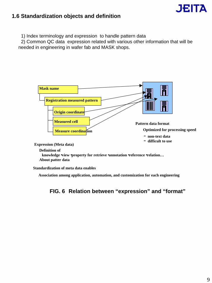
1.6 Standardization objects and definition
1) Index terminology and expression to handle pattern data2) Common QC data expression related with various other information that will be
needed in engineering in wafer fab and MASK shops.
Pattern data formatOptimized for processing speed
→non-text data→difficult to use
Registration measured pattern
Origin coordinate
Measured cell
Mask name
Measure coordination
Expression (Meta data)Definition of knowledge・view・property for retrieve・annotation・reference・relation…About patter data
Standardization of meta data enables
Association among application, automation, and customization for each engineering
Relation between “expression” and “format”FIG. 6

10
1.7 Relationship with the related standardization requirement
The activities of the overseas organizations that have complementary relationship are mentioned below:
・SEMI-Japan Reticle Data Management Task ForceThe standardization activities of micro patterning divisiona) It discusses the data-exchange method of the information relevant to a reticle.b) It intends to draft a guideline.c) It incorporates mask data into stepper recipe data preparation. It performs standardization of communication of reticle-related information among design ~ mask vender ~ wafer fab.
・SEMI-NA Mask Data Path Task ForceStandardization activities of UDM (Universal Data Mode) Working Group.a) It discusses the data-exchange method of the information relevant to a reticle.b) It intends to draft a guideline.c) In this, Open Access Coalition of Silicon Integration Initiative (Si2) is introduced.This consortium aims at offering the open standard to the IC design data access.
・MOPXE (Mask Order Processing in the Extended Enterprise)This activity about the mask supply chain is proposed from IMS (Intelligent Manufacturing System). The activity is carried out mainly in Europe.

11
2. General guideline
2.1 Sharing of reticle data
The standardization of expression of reticle related information including design information such as pattern data should be established, in order to make easy information exchange (it contains when it consists of two or more companies) relevant to the reticle, covering mask manufacture and wafer manufacture from a design.
The environment that can be utilized in common from design to wafer fab. must be established to fulfill the following conditions.
Conditions : 1. Reticle data and reticle-related data must be correlated with a hierarchic configuration. 2. Reticle data and reticle-related data must be delivered in a standardized method at each interface. 3. Reticle data and reticle-related data must be defined clearly in their contents. 4. Reticle data and reticle-related data must be stored for each fab. so that the required data can be taken out whenever necessary. 5. Reticle data and reticle-related data must be protected by the reasonable security system.
In Ver2, these include standardized expression to use design information such as pattern data.In SEMI-TF activities based on guideline ver1, standardized expression are
considered with XML technology.

12
2.2 The standardized expression for usability of pattern data
Apart from standardization of the data format of the pattern data itself, expression of referencing pattern data and other additional information that are associated in case pattern data is utilized should be standardized.
Pattern data itself is complexly structured and huge in volume. If it will be used in wafer fab, standardized expression is necessary considered from the point of view how engineers use it. Such expression works as indexing, annotating, relating with other useful information and combining several application. Figure 7 shows the image of this standardized expression. Engineering Chain Management must refer to Design Data through Quality Consideration, Process Consideration, and Cost Consideration.
Ex) Specification in desired pattern based on check Rule A1. Check Pattern (must be assessed impact on wafer)a. Minimum space in dense pattern
address center of the arealocation to be checked area to be observed
b. Gap between Line End and CornerAddress
center of the arealocation to be checked area to be observedgap definitionupper edgedown edge
c. Severe Line for performance
1. Check Pattern (must be assessed impact on wafer)
address center of the arealocation to be checked area to be observed
b. Gap between Line End and Corner
center of the arealocation to be checked area to be observedgap definitionupper edgedown edge
FIG. 7

13
3. Guideline for application3.1 Creative association among applications that use design information
The standardized representation should be considered with practical usage in order to make it possible to associate applications using design information.
For example, the Flexible Mask Specification Methodology proposed from TOSHIBA in 2002 Photo Mask Japan associates several concepts of applications. The Hot Spot Pattern is selected as most critical each reticle by verification tool. And Mask Specification is decided considering process window by simulation.
Pattern Data Usability Models for example....Flexible mask specification
DoseFo
cus
Lithography Window with mask errors
Devicepatterns
Hot spot patterns
Specificpatterns
S.Nojima et. al.(TOSHIBA ) /PMJ 2002
Flexibility identified patterns to decide mask specification
conventional
Pattern Data Usability Models
Design Data
Quality Considerations
ProcessConstraints
CostConsiderations
OtherKnowledge
Source
Engineering Chain Management(Integrated Process Optimization)
Usability Models would be proposed that are abstracted and constructed based on consideration about such examples.
Pattern Data Usability Models for example....Flexible mask specification
DoseFo
cus
DoseFo
cus
Lithography Window with mask errors
patternsHot spot patterns
Specificpatterns
S.Nojima et. al.(TOSHIBA ) /PMJ 2002
Flexibility identified patterns to decide mask specification
conventional
Pattern Data Usability ModelsPattern Data Usability Models
Design Data
Quality Considerations
ProcessConstraints
CostConsiderations
OtherKnowledge
Source
Engineering Chain Management(Integrated Process Optimization)
Usability Models would be proposed that are abstracted and constructed based on consideration about such examples.
FIG. 8

14
3.2 Comprehensive reusability in process module optimization
Standardized expression should be comprehensible for every process in a module and be reusable.
Recently process optimization is considered based on integrated process modules. Like this device process consists of multiple process modules. And each process module consists of many process steps like this. And then nowadays all process steps need to be aware of pattern layout dependency. For this reason process engineers must refer to huge storage of design information. If there are comprehensive models between process modules and Mega Storage of design information, they will be convenient to optimize for engineering chain management. As Figure 9 shows, they are thin layer that process engineers use to index design information. This guideline is intensive only on Reticle Data Management, but naturally, they would be reused in all process modules,
Process Optimization is consideredbased on Integrated Process Module.
Channel InterconnectIsolation Gate Contact
[1] Optimization of the Integrated process module
Each mask/wafer fabrication processes is compacted to one integrated process module that is categorized by quality and steps of fabrication. And this one module should be unified as a single function unit.
EtchLithoDepo Depo CMPCMP
InspectionInspectionInspectionInspectionInspectionInspection
All Process Steps need to be aware of pattern layout dependency
Mega Storage of Information in UDM and legacy in-house systems
Ver2.0: Comprehensive Usability Model for end-user application
Process Optimization is consideredbased on Integrated Process Module.
Channel InterconnectIsolation Gate ContactChannel InterconnectIsolation Gate Contact
[1] Optimization of the Integrated process module
Each mask/wafer fabrication processes is compacted to one integrated process module that is categorized by quality and steps of fabrication. And this one module should be unified as a single function unit.
EtchLithoDepo Depo CMPCMP
InspectionInspectionInspectionInspectionInspectionInspection
All Process Steps need to be aware of pattern layout dependency[1] Optimization of the Integrated process module
Each mask/wafer fabrication processes is compacted to one integrated process module that is categorized by quality and steps of fabrication. And this one module should be unified as a single function unit.
EtchLithoDepo Depo CMPCMP
InspectionInspectionInspectionInspectionInspectionInspection
All Process Steps need to be aware of pattern layout dependency
Mega Storage of Information in UDM and legacy in-house systemsMega Storage of Information in UDM and legacy in-house systems
Ver2.0: Comprehensive Usability Model for end-user application
FIG. 9

15
3.3 Strengthening linkage between design and manufacturing
Standardized expression should be able to strengthen linkage between design and manufacturing that can improve mutual optimization based on understanding relations with extensibility and reusability.
Corresponding to the future production system of design/manufacture cooperation, the standardized expression should be extensible so that the design side information such as DRC information, adding to pattern data, and the manufacture side information such as process margin evaluation can communicate mutually, and so that it is reusable to optimization of pattern data dependency even with processes other than lithography process. Like Figure 10, Design and Manufacturing are depending and encouraging each other. Through this circulating communication, optimizations will be improved. In Design these are Optimizations based on Manufacturability, Pattern Printability, and Process Specification. In manufacturing these are Optimizations based on Integrated Process Module Performance, Pattern Dependency, and Device Specification.
Enforcement of Linkages between Design and Manufacturing
Depending& Encouraging
Depending& Encouraging
Design
Ver.1.0 Ver.2.0
Manufacturing
Ver.1.0Ver.2.0
Optimization based onIntegrated Process Module,Pattern DependencyDevice Specification…
Defect Analysis
Order EntryRecipe Maintenance
Clustering of Equipment
Reticle Frame Data
Defect CoordinatesQC point Coordinates
Optimization based onManufacturability,Pattern PrintabilityProcess Specification…
(Design Rule Check)
(Pattern Image)(Electric Characteristics)
(Quality Control)(Robust Design)
(Flexible Methods)
Depending& Encouraging
Depending& Encouraging
Design
Ver.1.0 Ver.2.0
Manufacturing
Ver.1.0Ver.2.0
Optimization based onIntegrated Process Module,Pattern DependencyDevice Specification…
Defect Analysis
Order EntryRecipe Maintenance
Clustering of Equipment
Reticle Frame Data
Defect CoordinatesQC point Coordinates
Optimization based onManufacturability,Pattern PrintabilityProcess Specification…
(Design Rule Check)
(Pattern Image)(Electric Characteristics)
(Quality Control)(Robust Design)
(Flexible Methods)
FIG. 10
16
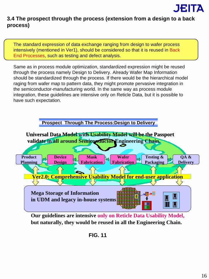
3.4 The prospect through the process (extension from a design to a back process)
The standard expression of data exchange ranging from design to wafer process intensively (mentioned in Ver1), should be considered so that it is reused in Back End Processes, such as testing and defect analysis.
Same as in process module optimization, standardized expression might be reused through the process namely Design to Delivery. Already Wafer Map Information should be standardized through the process. If there would be the hierarchical model raging from wafer map to pattern data, they might promote pervasive integration in the semiconductor-manufacturing world. In the same way as process module integration, these guidelines are intensive only on Reticle Data, but it is possible to have such expectation.
Prospect Through The Process:Design to Delivery
Universal Data Model with Usability Model will be the Passportvalidate in all around Semiconductor Engineering Chain.
ProductPlanning
DeviceDesign
MaskFabrication
WaferFabrication
Testing &Packaging
QA &Delivery
Mega Storage of Information in UDM and legacy in-house systems
Ver2.0: Comprehensive Usability Model for end-user application
Our Guidelines are intensive only on Reticle Data Usability Model,but naturally,they would be reused in all the Engineering Chain.
Ver2.0: Comprehensive Usability Model for end-user application
Our Guidelines are intensive only on Reticle Data Usability Model,but naturally,they would be reused in all the Engineering Chain.Our guidelines are intensive only on Reticle Data Usability Model,but naturally, they would be reused in all the Engineering Chain.
FIG. 11

17
4. The model of Global Joint Guidance
So that standard expression of RDM may cooperate with the standardization activities for the common interface of database storing information used in RDM, they should be considered to be convertible.
Exposure ToolOpen Functionfor Access EDA data
DataModel
API
API
DRCPattern DataUsability Model
OPC Tune
Defect Analysis
Inspection Recipi
temporary or extended data
All EDAData
P10
Pattern DataUsability Model Simulation
Positioning of Ver2
XML Representationof Standard TAG System
Standard TAG Systemfor user engineer's usage
Standard Data Modelfor all EDA Tool
example Exposure ToolOpen Functionfor Access EDA dataOpen Functionfor Access EDA data
DataModel
APIAPI
APIAPI
DRCPattern DataUsability Model
OPC Tune
Defect Analysis
Inspection Recipi
temporary or extended data
All EDAData
P10
Pattern DataUsability Model Simulation
Positioning of Ver2
XML Representationof Standard TAG System
Standard TAG Systemfor user engineer's usage
Standard Data Modelfor all EDA Tool
example
Temporary or extended data
FIG. 12

18
Contact JEITA Reticle Management Subcommittee Members
Sub-Leader
Leader
Role Name Company Address
Oki Electric Industry Co.,Ltd.
Toshio Onodera
TOSHIBA CORPORATIONTakashi Satoh
SANYO Electric Co.,Ltd.Toshiharu Matsuda
NEC Electronics CorporationMichio Honma
FUJITSU LIMITEDNorihiko Miyazaki
Nobuyuki Iriki
ROHM CO., LTD.Tamotsu Uga
Silicon Manufacturing CompanyWP Business Div.WP Business Dept.
Process & Manufacturing Engineering Center
Advanced ULSI EngineeringDept.Ⅱ
Semiconductor CompanyLSI BUEngineering Dept.
Corporate Strategic Planning Unit
Semiconductor GroupManufacturing TechnologyDevelopment Div.
MASK Technology Dept.
MASK Production Dept.VLSI Operation Div.
〒193-8550550-1 Higashi-asakawacho Hachiouji-shi TokyoTEL (0426)62-6234FAX (0426)62-6709E-M [email protected]
〒235-85228 Shinsugita Isogo-ku Yokohama-shi KanagawaYokohama OfficeTEL (045)770-3605FAX (045)770-3570E-M [email protected]
〒370-05961-1-1 Sakata Oizumi-Machi Ora-gun GunmaTEL (0276)61-8043FAX (0276)61-8836E-M [email protected]
〒211-86681753 Shimonumabe, Nakahara-Ku,Kawasaki Kanagawa
TEL (044)435-1406FAX (044)435-1870E-M [email protected]
〒197-083350 Fuchigami Akiruno-shi Tokyo(Akiruno Technology Center)TEL (042)532-2158FAX (042)532-2882E-M [email protected]
〒615-858521, Saiin Mizosaki-cho, Ukyo-ku, Kyoto, Japan
TEL (075)321-5120FAX (075)315-3231E-M [email protected]
〒312-85046-16-3 Horiguchi Hitachinakashi,Ibaraki-kenTEL (029)270-2185FAX (029)270-1792E-M [email protected]
RENESAS Technology Co.LSI Manufacturing UnitWafer Process EngineeringDevelopment Div.

19
Appendix
Guidelines for Reticle Data Management Ver.1.0(English Version)

20
Contents
1. Introduction 1.1 Background 1.2 Purpose 1.3 Scope 1.4 Standardization objects and definition1.5 Relationship with the related standardization Requirement 1.6 Requirement
2. General guideline 2.1 Sharing of reticle data2.2 Sharing that covers design mask fabrication and wafer fabrication
3. Guideline for application 3.1 B to B of order taking and ordering of mask3.2 Increase in efficiency of reticle defect analysis 3.3 Increase in efficiency of recipe maintenance in wafer fab. 3.4 Clustering of device in mask fab.3.5 Standardization of QC data
4. Standardization and implementation procedure 4.1 Activity organization and schedule
1. Introduction
21
The trend of speed requirements
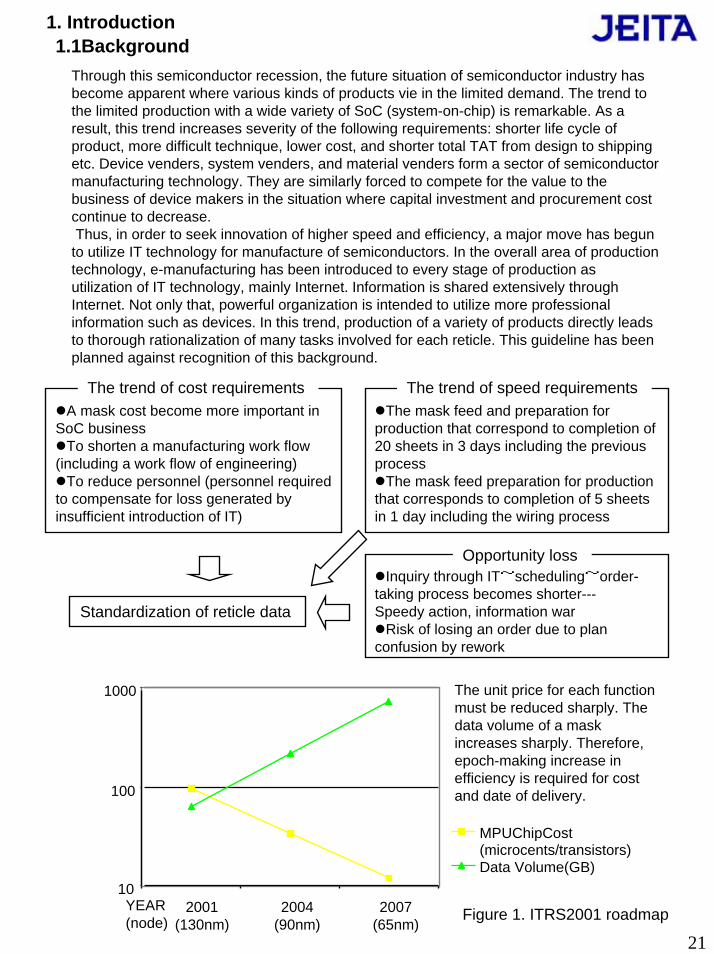
1.1BackgroundThrough this semiconductor recession, the future situation of semiconductor industry has become apparent where various kinds of products vie in the limited demand. The trend to the limited production with a wide variety of SoC (system-on-chip) is remarkable. As a result, this trend increases severity of the following requirements: shorter life cycle of product, more difficult technique, lower cost, and shorter total TAT from design to shipping etc. Device venders, system venders, and material venders form a sector of semiconductor manufacturing technology. They are similarly forced to compete for the value to the business of device makers in the situation where capital investment and procurement cost continue to decrease.Thus, in order to seek innovation of higher speed and efficiency, a major move has begun
to utilize IT technology for manufacture of semiconductors. In the overall area of production technology, e-manufacturing has been introduced to every stage of production as utilization of IT technology, mainly Internet. Information is shared extensively through Internet. Not only that, powerful organization is intended to utilize more professional information such as devices. In this trend, production of a variety of products directly leads to thorough rationalization of many tasks involved for each reticle. This guideline has been planned against recognition of this background.
The trend of cost requirements The mask feed and preparation for
production that correspond to completion of 20 sheets in 3 days including the previous process
The mask feed preparation for production that corresponds to completion of 5 sheets in 1 day including the wiring process
A mask cost become more important in SoC business
To shorten a manufacturing work flow (including a work flow of engineering)
To reduce personnel (personnel required to compensate for loss generated by insufficient introduction of IT)
Opportunity loss Inquiry through IT~scheduling~order-
taking process becomes shorter---Speedy action, information war
Risk of losing an order due to plan confusion by rework
Standardization of reticle data
10
100
1000
2001(130nm)
2004(90nm)
2007(65nm)
YEAR(node)
MPUChipCost(microcents/transistors)Data Volume(GB)
The unit price for each function must be reduced sharply. The data volume of a mask increases sharply. Therefore, epoch-making increase in efficiency is required for cost and date of delivery.
Figure 1. ITRS2001 roadmap

22
1.2 PurposeAs mentioned in 1.1 Background, the speed from design to merchandising is critical for digital electric household appliance and Internet-related devices. These devices are represented by SoC. Especially, in order to cope with the limited production with a wide variety of products, the speed for reticle tasks becomes critical. They include reticle feed, reticle-related preparation in manufacture, analysis of defect caused by reticle etc. The information related to reticle covers widely design, mask manufacture, and wafer manufacture. Despite a progress of partial automation, many exchanges of data rely on a conventional method such as telephone, resulting in loss of person-hours and time.
This guideline is primarily intended to address this issue by increasing efficiency consistently based on standardization that ranges from design, to mask manufacture, and to wafer manufacture.
Secondly, this guideline is intended to support efficient deployment of new automation application business of device and production system venders, by enabling them to share information among the systems in the innovation where a variety of product are produced in a small quantity.
Design
Mask Fab
Wafer Fab
0) Business(environment)
5) Security
3) Recipe Maintenance
2) Defect Analysis
4) Clustering Equipments in Mask Fab
1) B to B
Items to be improved:

23
1.3 Scope
The following items, (1) through (5), are related to interfaces for information exchange(necessary minimum data structure for universal use of information) .The scope proposes the guidelines for standardization of these interfaces.
(1)Production schedule, WIP tracking(2) or (4)Quality Control in wafer fab.(recipe, device management, process monitor) (3)Interchange and utilization of inspection, measurement data, and defect data(5)Preparation of recipe of device in mask fab. However, we exclude device H/W that is used for pattern data(graphic data required for CAD, OPC, PSM, TEG, and exposure/inspection),
communication medium (network circuit, protocol), and device that is used forinformation interchange. In addition, the interfaces of above-mentioned
(1) through (5) are so structured as to permit the mutual reuse of information.
Logic, circuit design
EB conversion
EB exposure
Mask shipment
Mask order sheetInspection specification
Transport
MaskAcceptanceIncomming QA
DRC
Frame generation, frame specification
Design department
Production control department
Mask manufacturing department
Wafer manufacturing department
In-house processing
Frame specification
Inspection data
Mask order sheetInspection specification
Wafer fab. Mask fab.
1
3
2
5
4
DesignPattern data are excluded
Standardization target
Process engineering department
Data serverGDSII data transfer server
ORC OPC generation
Inspection data
Inspection Recipe
Dummy generation
Mask Inspection
Specification code registrationFrame specificationapproval, issue
Pattern design
Dummy OPC Frame
24
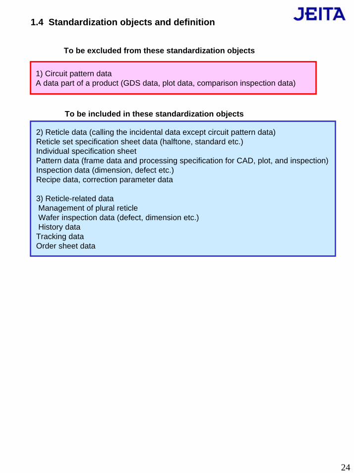
1.4 Standardization objects and definition
1) Circuit pattern dataA data part of a product (GDS data, plot data, comparison inspection data)
To be excluded from these standardization objects
To be included in these standardization objects
2) Reticle data (calling the incidental data except circuit pattern data) Reticle set specification sheet data (halftone, standard etc.) Individual specification sheet Pattern data (frame data and processing specification for CAD, plot, and inspection) Inspection data (dimension, defect etc.) Recipe data, correction parameter data
3) Reticle-related dataManagement of plural reticleWafer inspection data (defect, dimension etc.) History data
Tracking data Order sheet data

25
Wafer Fab.
Design house
Mask Fab.
Reticle order sheet
Reticle specification sheet
Delivery control sheet
Reticle data fabrication sheet
Defect inspection sheet Reticle shipment inspection sheet Frame data sheet
Wafer map sheet
Frame data sheet
Wafer map data sheet Frame fabrication sheet
Exposure Equipment recipe sheet CD measurement Equipment recipe sheet
Defect inspection Equipment
Alignment measurement Equipment recipe sheet
Defect inspection Equipment result sheet
Delivery/change sheet
Defect correction sheet
CD inspection sheet
Coordinate inspection sheet
Supplement The above-mentioned standardization objects are controlled by the example sheets
mentioned below.
CAD, WP device, WP
Mask vender, WP
Mask vender, mask device
CAD, WP device, WP
Related to frame data (exposure device mark, inspection device mark, TEG, etc.)1)WP device vender (exposure device, CD, alignment, defect inspection device) 2)CAD (frame CAD vender) 3)Wafer fab. user (JEITA)
Related to order-taking and ordering, specification, delivery, change, inspection result1)Mask vender 2)Wafer fab. user (JEITA)
Related to reticle data handling in mask house 1)Mask vender 2)Mask device vender 3)Selete

26
1.5 Relationship with related standardization
This guideline deals with the interface of the data exchange of the informationrelevant to the reticle except pattern data. The activities of the overseas organizationsthat have complementary relationship are mentioned below..
(1) SEMI-Japan Reticle Data Management Task Force The standardization activities of micro patterning division ·It discusses the data-exchange method of the information relevant to a reticle.·It intends to draft a guideline.·It incorporates mask data into stepper recipe data preparation. It performs standardizationof communication of reticle-related information among design~mask vender~ wafer fab.
(2) SEMI-NA Mask Data Path Task Force Standardization activities of UDM(Universal Data Model) Working Group ·It discusses the data-exchange method of the information relevant to a reticle. ·It intends to draft a guideline.·In this, Open Access Coalition of Silicon Integration Initiative (Si2) is introduced. This consortium aims at offering the open standard to the IC design data access.
(3) MOPXE(Mask Order Processing In the eXtended Enterprise). ·This activity about the mask supply chain is proposed from IMS (Intelligent Manufacturing System). The activity is carried out mainly in Europe

27
systematization oftechnology
Requirement for quality Flexibility(to address a change)
Security
Low-pricing(cost reduction)
Speed(to shorten total TAT)
Growth of business (ROI)
Requirements forestablishment ofcommon platform
Requirements for total IT integration
1.6 Requirement for establishment of common languagefor reticle-related information
The requirements for SoC business of small production of many kinds of products lead to requirement for establishment of common language through requirementfor total IT utilization. Utilization of many techniques that is based on XML in IT areamust be so developed as to support the requirements for SoC business.
1) Technical systematization The speed of technical accumulation is accelerated by IT technology. For that purpose, technical systematization that aims at high availability is required. The reticle-related information must be formulized in terminology/definition/methodology about several aspects of utilization, accumulation, and exchange in a wide area.
Litho process
Litho Equip.
Lithoprocess
Mask manufacture
Mask Equip.
Maskprocess
Recipemaintenance
Equipmentsclustering
Patterndesign
Chippattern
Framepattern
Design
Data preparation
Order-taking and ordering
Delivery control QC data
BtoB
Quality standard
Defect analysis
Productionplan
Domain ofbusiness unit
Domain of technology
Domain ofapplication
Necessity of interoperability among various domains
Reticle-related information is used by the entire area of domains through partial relationship.
Necessity of semantic interoperability is large.

28
Different kinds ofinformation sources
Information sourcebased on common platform
Standard data exchangeof XML base
Application
ApplicationApplication
Application
Informationsource
Informationsource
Informationsource
1) Application eliminates the connection cost,and emphasizes functions that create values.It is possible to obtain the development flexibilitythat overcomes the speed of obsolescence. Both distribution and IP of application are attempted.
2) By controlling the meaning and source of information, it is possible to measure the value ofinformation supplied and to activate business.
3) It is possible to instantly monitor various informationthat is generated widely and asynchronously in Internet.
4) Data are standardized by XML and wrapped for dataexchange. It is possible to permit Inconsistence of variousdata between different kinds of information sources. Thus, it promotes development of individual information sources.
2) FlexibilityProduction technology must continue to innovate obsolete technology to cope withan ever-changing market, and IT technology must be easily updated. In addition,
the reticle-related information is generated and use in various aspects, and a data modelwith high flexibility is required.
4) Security The information about a reticle must be maintained at high security for a customer. Share information must be systematized to set up security management that is partitionedappropriately and efficiently for various security requirements and usability requirements.
3) Return of investment in businessActivation of information service based on standardization is required to reducethe introduction cost. Owners and users should be clarified according to information
classification. Collaboration should be realized among device makers, mask makers, equipment makers, and system makers. For that purpose, various business modelshould be built where security is precisely set up and license and fees are established.
Security managementtechnique bases onprecise classification
Different kinds ofinformation sources
Information sourcebased on common platform
Standard data exchangeof XML base
Informationsource
Informationsource
Informationsource
Different kinds ofinformation sources
Information sourcebased on common platform
Standard data exchangeof XML base
Informationsource
Informationsource
Informationsource

29
5) Quality As the technology becomes more difficult, lack of consideration about quality generates the maximum loss. Application of IT technology to semiconductorproduction technology is not limited to a superficial support for quality control
. It needs to support by incorporating analysis, which was difficult because ofshortage of labor in the past. The requirements for quality of a reticle are also
increased. Therefore, efficient development should be supported.
Visualization of potential influence relationship
Preset filter
6) Cost In order to reduce the cost for every reticle under small production of various products, it is necessary to eliminate every loss that is dispersed and generatedin an extensive area and to obtain an integral effect. Not only that, it is necessaryto establish standardization that is suitable for Internet technology in order to
realize a wide information exchange inexpensively.7) TAT In order to make it contribute to ultimate product TAT realization, you should eliminate break and leakage in a total work flow. For that purpose, you should consider main stream design data that range from design to mask manufactureand to wafer manufacture. Not only that, you should include information that is
information generated derivatively and consider possibility of wide reuse.Parallel processing of preparation and postprocessing Conversion task
loss loss
lossloss
lossloss
loss loss

30
2. General guideline
2.1 Sharing of reticle data
The environment that can be utilized in common from design to wafer fab. must be established being fulfilled the following conditions.
Conditions : 1. Reticle data and reticle-related data must be correlatedwith a hierarchic configuration.
2. Reticle data and reticle-related data must be deliveredin a standardized method at each interface.
3. Reticle data and reticle-related data must be defined clearly in their contents. 4. Reticle data and reticle-related data must be stored for each fab. so that the required data can be taken out whenever necessary. 5. Reticle data and reticle-related data must be protected by the reasonable security system.
SpecsSheet
Delivery Info.
OrderEntry
Qualitydata(CD)
QualityData(Defect)
Design House
Mask Fab.
Wafer Fab.
ExampleExample
·Minimum data structurerequired to share information
Platform ·Security ·Data matching
·It extends freely according to a business
·Standardized information isavailable at any time. ·Connection isunrestricted

31
2.2 Outline of shared guideline covering design, mask manufacture and wafer manufacture
Interchange of various data that were explained above has been built by individual association at B to B until now. The left-hand figure shows continuing building of individualassociation, while the right-hand figure is based on standardization of processes
that ranges from design of reticle data and reticle-related data to mask manufacture and to wafer manufacture. The individual know-how and the common data exchange are associated and controlled respectively, and overall complex processes can be simplified.
Design MaskWaferFab. Design Mask
WaferFab.
Mask fab. Wafer fab.
Design houseMask fab
Wafer fab. Design house.
Guideline related to frame data(exposure device mark, inspection
device mark etc.)(toward creation of standardization format)Guideline for design (technology unit)and photolitho manufacture standard
(wafer, reticle accuracy)(toward creation of standardization format)
Guideline for mask order-taking and ordering system and data handling(toward creation of standardization
format) (ref: P10)
B to B Shared data
Chip sizeBlock configurationReticle set markCD (On wafer/reticle)DefectOrthogonalityShrinkAlignment mark
Items for standardization
QC flow Data handling

32
3. Guidelines for Applications3.1 Order-taking and Ordering of Mask(1)Guideline for Order-taking and Ordering of Mask
Mask order-taking and ordering information must be shared from design to mask fab. and to wafer fab
For data handling, a business model must be flexible enough to meet the requirementsof both parties concerning various formats for drawing, text, GDS, Mebes etc.
The status report of each mask must be shared among order-taking, ordering, and production control of reticle database in order to report mask making progress reportand forecast delivery it for customer. This mask supply is and will be a key for a fine patterned device. This will be an issue whether you produce a mask in-house or not.
[Effects] •You can service all customers more quickly than now•You can reduce system development cost
Design MaskWafer Fab.
[Common items for order-taking and ordering of mask] 1) Design data (drawing, GDS II, Mebes etc) (including frame data) 2) Manufacture request sheet (a masking name, new edition, revision, reprint, size, pellicle class, specified date of delivery, destination) 3) Manufacture conditions (manufacture data specification, exposure data arrangementspecification, manufacture specification, and inspection specification)
4) Progress 5) Specification (grade) 6) Quality (dimension, arrangement, defect, phase difference, transmittance) 7) Inquiry
Shared environment of
order-taking and ordering

33
Production planat wafer fab.
(2) Mask Progress report and Delivery forecast program
Mask fab. should offer wafer fab. the updated information including delivery scheduleof rework of reticle manufacture. Both should offer the standardized interface.
Reticle data management ―Just-in-time program
Timely prediction of delivery(● part) is added to the conventional B to B (○ part)in the standardization. Thus, B to B cooperation can eliminate waste that is observedby a customer.
LSI chip delivery date(specified by a LSI chip customer)
Keepdelivery date of chip
Improved accuracy of production plan
Defect occurrenceduring manufacture
Preset delivery dateat the order of the reticle
Change (delay)information
Rework plan simulation
Reticle manufacture
Wafer fab. Productionplan check
Production planat mask fab.
Progress report during manufacture
Observance ofdelivery date of reticle
Wafer fab. Productionplan re-simulation

34
(3) Mask Ordering Data forXML (Structured Reticle Data for Order)
Mask OrderMask Order
Mask NameMask Name
Order codeOrder code
Accountinginfo.
Accountinginfo.
Logisticinfo.
Logisticinfo.
ProcessingTool
ProcessingTool
ProcessingSpec.
ProcessingSpec.
Manufacturespec code
Manufacturespec code
Data processingcode
Data processingcode MaterialMaterial ToleranceTolerance Processing
Tool
ProcessingTool
Manufacturecontrol code
Manufacturecontrol code
Logisticinfo.
Logisticinfo.
Worksheet
Worksheet
Manufactureprocess code
Manufactureprocess code
Qualityinfo.
Qualityinfo.
Toolinfo.
Toolinfo.

35
3.2 Increase in efficiency of analysis of reticle defect
The reticle data and reticle-related data must be ready for wafer fab. to referthose for analysis of quality in wafer fab. (defect, dimension etc.) whenever necessary.
Example 1) You use the reticle data and reticle-related data so that you can judge whether the quality in wafer fab. originates in a reticle or not.
Example 2) You correlate quality information of a reticle with that of wafer so thatyou can increase efficiency of the process improvement of reticle manufacture.
[Examples of effects] · You can improve the quality of mask· You can increase efficiency of the quality analysis in wafer fab. · You can clarify the criteria of quality, optimize mask production process, and
reduce a manufacturing cost· You can reduce the cost to develop a tool to analyze correlation between mask
quality and wafer printing characteristics. [Example of methods] · You feed back the wafer printing result to the mask fab. and accumulate the
data about correlation between mask quality and wafer printing characteristics · You feed forward the quality information of mask manufacture process to the
wafer fab. and utilize it for the quality analysis at wafer fab.
Wafer Fab. Mask Fab.
Coordinate transformation Mask
Fab.WaferFab.
Common language
Mask nameWafer quality data
Dimension data
Others
Defect dataPosition data
Defect informationon wafer
Defect informationand correction
information on reticle
Wafer quality inspection Tool
Reticle quality inspection Tool Reticle repair Tool
Mask nameDimension dataDefect dataPosition data
Mask quality data
Others
Coordinate transformation

36
3.3 Increase in efficiency of recipe build in wafer fab
Guideline of Standardized Reticle design information and QC datato make reusable it for recipe build in Wafer Fab.
1) The data that are related to recipe build of systems, such as exposure tools, inspection tools, APC, MES, etc. are generated in various data sources throughout the design shop, mask fab. and wafer fab. In order to address various quality requirements in the future, you need a flexible method based on the common formats of data.
[Effects] · The time of recipe building at wafer fab. will become quick.· The cost for developing recipe build system will be minimized.
[Methods] · Mask flame information, mask quality information, wafer map and sample
plans are provided as standardized format data from each site. Recipe builders import these data and make recipe.
QC DataFlame Information
Design Mask Fab
Conversion
Wafer Fab
Conversion Conversion
Exposure ToolRecipe
CD SEMRecipe
Defect InspectionRecipe
Wafer Map,Sample plan, etc
Standardization
RecipeBuilder A
RecipeBuilder B
RecipeBuilder C

37
3.4 Data sharing within mask fab.
The data and information within Mask Fab.; inspection, defect correct and review tool, should be able to be shared for mutual reference of data as necessary.
1) Reticle defect correction process use many tools;inspection, defect correction and review. This correction will be efficient, if tools can share there results and recipe.
[Effects] - Can shorten the time to create a recipe at the process of mask defect inspection, defect
correction and review by reuse of information i.e. coordinates information etc. - Can reduce the development cost of a recipe by preparing standard or flexible data format- Can improve mask quality by integrate information related to mask defect.
[Methods] - Collect, store, report and analyze the information about mask defect and processing
information.- Associate and integrate the information about mask defect at wafer manufacture process
and the information at mask manufacture process.
ReviewReview
InspectionInspection
RepairRepairRepair recipe
Review recipe
Defect Data
Repair Data
Defect Record
Repair Record
Review Record
Inspection recipe
Automatic
Automatic
MESMES
DBDBDBDB
DBDB

38
Example) XML Data Tree of Inspection Tool
Process No Tool Information_n
Basic
Inspection Result_n
Start Date
Start Time
Complete Date
Complete Time
Processing Hours
Origin_n
Tool_No
Date of Preparation
Data of Inspection Area
Operator of Preparation
Reference Area DB
Date
Time
Chip Number
Chip Size Chip Size_x
Rotation
Mirror
Flip
Size_x
Size_y
Chip_n_x
Chip_n_y
Chip Size_y
Basic Area DB Coordinate Definition
Image Data
Coordinate_y
Coordinate_x
Inspection Method
Tool Information_X
1)
3)
4)
Date/Time Stamps
Inspection Area
Defect No. n Position_x
Position_y
Judge
Image Data n
Summary of Detection
Operator
Inspection Result n Summary
Total No
Class Code n: Total No
Defect No. X
Judge
Repair_n
Image Data
Fatal/Repair/No need Class Code
Evaluation Updated Evaluation
Recipe
Mode/Level Customer/Supplier Agreement
Name of Recipe
Inspection Result X
Data Post Repair QC
1)
2)
4)
2)
Date/Time Stamps Start Date
Start Time
Complete Date
Complete Time
Processing Hours

39
At B to B, standards information should be exchanged in the standardized items.
3.5 Reusable QC Data
1. Classification of information 1) Wafer Fab. standards information - Order sheet - Spec sheet 2) Mask Fab. standards information - QC sheet 2. Merit: Improvement of productivity and reduction of cost
Methods :Expansion of reusability of QC information by standardization of different section(definition and usage of QC data at Wafer, Mask and Design)
1) As to QC data, you standardize such components that can be stratified and shared. You should deal with data handling in a standardized method.
2) You should use classification and stratification for communalization. You shouldpromote first the area that is easy to communalize, namely that is highly commonor highly abstract.
dictionary
procedure
Imagedata
Additionaldata
Patterndata
QC data
(with structure)
Calibrationdata
Framework
deliveryspec.
Processspec.
Geometrystructure
QC Data Standardization
Recipe Parameter Data Matching
Spec Sheet
Focused
Defect AnalysisOrder Entry
Recipe Maintenance Clustering of Equipment
Data Matching
Introduced Topics QC data Standardization

40
Examples of sharing of procedure and pattern data
dictionary
Price-data
Imagedata
Addition-naldata
Patterndata
QC data
(with structure)
Calibrationdata
Framework
deliveryspec.
Processspec.
Geometrystructure
QC Data Standardization
Recipe Parameter Data Matching
Spec Sheet
Focused
Defect AnalysisOrder Entry
Recipe Maintenance Clustering of Equipment
Data Matching
Introduced Topics QC data Standardization
Dictionary
Procedure PatternDataGDSII, Mebes etc
XSD
Conversion Rule
XSL
ExampleExample
TranslatorTranslator
TranslatorTranslator
FormatterFormatter
QC Data With StructureQC Data With Structure
TranslatorTranslator
Reticle Data Management
Target

41
Example) QC data of order-taking and ordering of mask
1) Shipped Mask Number(for each type of product, each grade, each technology, each size, new edition, revision, reprint)
2) Just-in-time Delivery Reticle Ratio 3)TAT 4)Quality (CD:uniformity/mean to target, Distortion, Defect) 5)Tool (Tool Up Ratio, QC/Pre Maintenance result ) 6)Failure data
* : Data must be read on a platform. Production control and quality control should be shown daily, weekly, and monthly. Those data must be updated to reticle production plan and development plan.

42
Contact JEITA Reticle Management Subcommittee Members
Sub-Leader
Leader
Role Name Company Address
Oki Electric Industry Co.,Ltd.
Toshio Onodera
TOSHIBA CORPORATIONTakashi Satoh
SANYO Electric Co.,Ltd.Toshiharu Matsuda
NEC Electronics CorporationMichio Honma
FUJITSU LIMITEDNorihiko Miyazaki
Nobuyuki Iriki
Matsushita Electric IndustrialCo., Ltd.
MITSUBISHI ELECTRIC CORPORATION
Masayoshi Mori
Tadashi Imoriya
Silicon Manufacturing CompanyWP Business Div.WP Business Dept.
Process & Manufacturing Engineering Center
Advanced ULSI EngineeringDept.Ⅱ
Semiconductor CompanyLSI BUEngineering Dept.
Corporate Strategic Planning Unit
Semiconductor GroupManufacturing TechnologyDevelopment Div.
MASK Technology Dept.
Semiconductor CompanyCorporate Manufacturing& Development Div.
Design Support Group
ULSI Development CenterULSI Process
Integration Dept.
〒193-8550550-1 Higashi-asakawacho Hachiouji-shi TokyoTEL (0426)62-6234FAX (0426)62-6709E-M [email protected]
〒235-85228 Shinsugita Isogo-ku Yokohama-shi KanagawaYokohama OfficeTEL (045)770-3605FAX (045)770-3570E-M [email protected]
〒370-05961-1-1 Sakata Oizumi-Machi Ora-gun GunmaTEL (0276)61-8043FAX (0276)61-8836E-M [email protected]
〒211-86681753 Shimonumabe, Nakahara-Ku,Kawasaki Kanagawa
TEL (044)435-1406FAX (044)1870E-M [email protected]
〒197-083350 Fuchigami Akiruno-shi Tokyo(Akiruno Technology Center)TEL (042)532-2158FAX (042)532-2882E-M [email protected]
〒601-841319 Nishikujokasugamati Minami-ku
Kyoto-shi KyotoTEL (075)662-7357FAX (075)662-6154E-M [email protected]
〒664-86414-1 Zuihara Itami-shi HyogoTEL (0727)84-7532FAX (0727)80-2597E-M [email protected]
〒312-85046-16-3 Horiguchi Hitachinakashi,Ibaraki-ken
TEL (029)270-2185FAX (029)270-1792E-M [email protected]
RENESAS Technology Co.LSI Manufacturing UnitWafer Process EngineeringDevelopment Div.