gtx 680 kepler whitepaper -...
TRANSCRIPT

Whitepaper
NVIDIA GeForce GTX 680 The fastest, most efficient GPU ever built.
V1.0
Table of Contents
Table of Contents .......................................................................................................................................... 1
Introduction .................................................................................................................................................. 3
Performance Per Watt .................................................................................................................................. 3
Kepler Architecture In-Depth (GeForce GTX 680) ......................................................................................... 5
GPC ............................................................................................................................................................ 6
Next Generation SM (SMX) Overview ....................................................................................................... 7
Next Generation SM (SMX) Architectural Details ................................................................................... 10
PolyMorph Engine 2.0 ............................................................................................................................. 11
L2 Cache .................................................................................................................................................. 12
Bindless textures ..................................................................................................................................... 13
World’s Fastest GDDR5 ........................................................................................................................... 14
GPU Boost ................................................................................................................................................... 15
Adaptive VSync ........................................................................................................................................... 17
FXAA ............................................................................................................................................................ 20
TXAA ............................................................................................................................................................ 23
New Display/Video Engine .......................................................................................................................... 26
NVENC ..................................................................................................................................................... 26
Conclusion ................................................................................................................................................... 28

3
Introduction
Since our inception, NVIDIA has strived to bring the highest quality 3D graphics to gamers, with each
new generation pushing the performance envelope, and delivering the latest graphics effects and
stunning visuals for the PC platform. Enthusiast-class PC games that took full advantage of our most
recent Fermi GPU generation were able to incorporate highly detailed, geometrically complex 3D
graphics scenes, and convincing character renderings, animations, and physical simulations.
With the introduction of NVIDIA’s latest GPU architecture, codenamed “Kepler,” our goal was to
continue to push the limits in graphics processing capabilities, and also create an extremely power-
efficient GPU.
NVIDIA’s Kepler architecture builds on the foundation first established in 2010 with NVIDIA's Fermi GPU
architecture. Fermi introduced an entirely new parallel geometry pipeline optimized for tessellation and
displacement mapping. This made it possible for games such as Battlefield 3, Batman: Arkham City, and
Crysis 2 to use richly detailed characters and environments while retaining high performance. Kepler
continues to provide the best tessellation performance and combines this with new features specifically
designed to deliver a faster, smoother, richer gaming experience.
The first GPU based on our new Kepler architecture, codenamed “GK104,” is not only our highest
performing GPU to date, it is also the most efficient in terms of power consumption. GK104 is fabricated
on an optimized 28nm process, and every internal unit was designed for the best perf/watt possible. The
first product being introduced based on GK104 is the GeForce GTX 680.
The introduction of NVIDIA’s Kepler GPU architecture will allow game developers to incorporate even
greater levels of geometric complexity, physical simulations, stereoscopic 3D processing, and advanced
antialiasing effects into their next generation of DX11 titles.
But the next generation of PC gaming isn’t just about clock speeds, raw performance, perf/watt, and
new graphics effects. It’s also about providing consistent frame rates and a smoother gaming
experience. In this whitepaper you will learn about the new smooth gaming technologies implemented
in Kepler to enable this.
Performance Per Watt
When designing our prior generation Fermi GPU architecture, NVIDIA engineers focused on dramatically
improving performance over the Tesla (GT200) GPU generation, with special emphasis on geometry,
tessellation, and compute performance for DirectX 11. Though managing power consumption was an
important consideration during Fermi’s development, achieving breakthrough levels of DX11
performance was the primary objective.
For Kepler we took a different approach. While maintaining our graphics performance leadership was
still the most important goal, the overarching theme driving Kepler’s design was dramatically improving

4
performance per watt. NVIDIA engineers applied everything learned from Fermi to better optimize the
Kepler architecture for highly efficient operation, in addition to significantly enhanced performance.
TSMC’s 28nm manufacturing process plays an important role in lowering power consumption, but many
GPU architecture modifications were required to further reduce power consumption while maintaining
high performance.
Every hardware unit in Kepler was designed and scrubbed to provide outstanding performance per watt.
The most notable example of great perf/watt can be found in the design of Kepler’s new Streaming
Multiprocessor, called “SMX.” In SMX we saw a large opportunity to reduce GPU power consumption
through a new architectural approach. For improved power efficiency, the SMX now runs at graphics
clock rather than 2x graphics clock; but with 1536 CUDA cores in GK104, the GeForce GTX 680 SMX
provides 2x the performance per watt of Fermi’s SM (GF110). This allows the GeForce GTX 680 to deliver
revolutionary performance/watt when compared to GeForce GTX 580:
SMX’s design for power efficiency is discussed in more depth in the “Next Generation SM” section
below.

5
Kepler Architecture In-Depth (GeForce GTX 680)
Like Fermi, Kepler GPUs are composed of different configurations of Graphics Processing Clusters
(GPCs), Streaming Multiprocessors (SMs), and memory controllers. The GeForce GTX 680 GPU consists
of four GPCs, eight next-generation Streaming Multiprocessors (SMX), and four memory controllers.
Figure 1: GeForce GTX 680 Block Diagram

6
In GeForce GTX 680, each GPC has a dedicated raster engine and two SMX units. With a total of eight
SMX units, the GeForce GTX 680 implementation has 1536 CUDA Cores.
GeForce GTX 680’s memory subsystem was also completely revamped, resulting in dramatically higher
memory clock speeds. Operating at 6008MHz data rate, GeForce GTX 680 offers the highest memory
clock speeds of any GPU in the industry.
Tied to each memory controller are 128KB L2 cache and eight ROP units (each of the eight ROP units
processes a single color sample). With four memory controllers, a full GeForce GTX 680 GPU has 512KB
L2 cache and 32 ROPs (i.e., 32 color samples).
We’ll be discussing the SMXs, ROPs and other units in greater detail in the following pages. We assume
you already have a basic understanding of the pipeline changes introduced with NVIDIA’s GPC
architecture first implemented in Fermi. If you are not well versed in NVIDIA’s GPC architecture, we
suggest you first read the GF100 whitepaper.
The following table provides a high-level comparison of Kepler vs. previous generation NVIDIA GPUs:
GPU GT200 (Tesla) GF110 (Fermi) GK104 (Kepler)
Transistors 1.4 billion 3.0 billion 3.54 billion
CUDA Cores 240 512 1536
Graphics Core Clock 648MHz 772MHz 1006MHz
Shader Core Clock 1476MHz 1544MHz n/a
GFLOPs 1063 1581 3090
Texture Units 80 64 128
Texel fill-rate 51.8 Gigatexels/sec 49.4 Gigatexels/sec 128.8 Gigatexels/sec
Memory Clock 2484 MHz 4008 MHz 6008MHz
Memory Bandwidth 159 GB/sec 192.4 GB/sec 192.26 GB/sec
Max # of Active Displays 2 2 4
TDP 183W 244W 195W
The overall configuration of GTX 680 was chosen to provide a large increase in shader and texture
horsepower vs. the GTX 580, while maintaining per clock operand throughputs for most other metrics
(which also benefit from the increased core clock frequency).
GPC
The GPC continues to be the dominant high-level hardware block in Kepler. With its own dedicated
resources for rasterization, shading, texturing, and compute, most of the GPU’s core graphics functions
are performed inside the GPC. GeForce GTX 680 contains four GPCs, delivering 32 pixels per clock.

7
Next Generation SM (SMX) Overview
The SM is the heart of NVIDIA’s unified GPU architecture. Most of the key hardware units for graphics
processing reside in the SM. The SM’s CUDA cores perform pixel/vertex/geometry shading and
physics/compute calculations. Texture units perform texture filtering and load/store units fetch and
save data to memory. Special Function Units (SFUs) handle transcendental and graphics interpolation
instructions. Finally, the PolyMorph Engine handles vertex fetch, tessellation, viewport transform,
attribute setup, and stream output.
One of the keys to GeForce GTX 680’s extraordinary performance is the next generation SM design,
called SMX. SMX contains several important architectural changes that combine to deliver
unprecedented performance and power efficiency.
To understand SMX performance, it helps to start by comparing the chip level unit counts for GeForce
GTX 580 (containing 16 SMs) to GeForce GTX 680 (containing 8 SMXs):
GPU GF110 (Fermi)
GK104 (Kepler)
Ratio Ratio (w/ clk freq)
Total unit counts :
CUDA Cores 512 1536 3.0x
SFU 64 256 4.0x
LD/ST 256 256 1.0x
Tex 64 128 2.0x
Polymorph 16 8 0.5x
Warp schedulers 32 32 1.0x
Throughput per graphics clock :
FMA32 1024 1536 1.5x 2.0x
SFU 128 256 2.0x 2.6x
LD/ST (64b operations) 256 256 1.0x 1.3x
Tex 64 128 2.0x 2.6x
Polygon/clk 4 4 1.0x 1.3x
Inst/clk 32*32 64*32 2.0x 2.6x
At the chip level, the per-clock throughput for key graphics operations (FMA32, SFU operations, and
texture operations) have all been increased substantially, while other operations retain per-clock
throughput equal to GeForce GTX 580. GeForce GTX 680’s substantially higher clock frequency provides
a further throughput boost for all operations.

8
In GeForce GTX 680, for area efficiency reasons, we chose to divide the aggregate horsepower into 8
total SMX units (rather than dividing the aggregate horsepower into 16 SM units as we did in GeForce
GTX 580). Considering this and the other factors above, the per-SMX unit count and throughput can be
compared as follows:
GPU GF110 (Fermi)
GK104 (Kepler)
Ratio Ratio (w/ clk freq)
Per SM unit counts :
CUDA Cores 32 192 6.0x
SFU 4 32 8.0x
LD/ST 16 32 2.0x
Tex 4 16 4.0x
Polymorph 1 1 1.0x
Warp schedulers 2 4 2.0x
Throughput per graphics clock :
FMA32 64 192 3.0x 3.9x
SFU 8 32 4.0x 5.2x
LD/ST (64b operations) 16 32 2.0x 2.6x
Tex 4 16 4.0x 5.2x
Polygon/clk 0.25 0.5 2.0x 2.6x
Inst/clk 32*2 32*8 4.0x 5.2x
See below for the block diagram illustration of the functional units in SMX.

9
Figure 2: GeForce GTX 680 SMX

10
Next Generation SM (SMX) Architectural Details
To feed the execution resources of SMX, each unit contains four warp schedulers, and each warp
scheduler is capable of dispatching two instructions per warp every clock.
More importantly, the scheduling functions have been redesigned with a focus on power efficiency. For
example: Both Kepler and Fermi schedulers contain similar hardware units to handle scheduling
functions, including, (a) register scoreboarding for long latency operations (texture and load), (b) inter-
warp scheduling decisions (e.g., pick the best warp to go next among eligible candidates), and (c) thread
block level scheduling (e.g., the GigaThread engine); however, Fermi’s scheduler also contains a complex
hardware stage to prevent data hazards in the math datapath itself. A multi-port register scoreboard
keeps track of any registers that are not yet ready with valid data, and a dependency checker block
analyzes register usage across a multitude of fully decoded warp instructions against the scoreboard, to
determine which are eligible to issue.
For Kepler, we realized that since this information is deterministic (the math pipeline latencies are not
variable), it is possible for the compiler to determine up front when instructions will be ready to issue,
and provide this information in the instruction itself. This allowed us to replace several complex and
power-expensive blocks with a simple hardware block that extracts the pre-determined latency
information and uses it to mask out warps from eligibility at the inter-warp scheduler stage.
We also developed a new design for the processor execution core, again with a focus on best
performance per watt. Each processing unit was scrubbed to maximize clock gating efficiency and
minimize wiring and retiming overheads.

11
The biggest visible change for the processor core is the elimination of shader clock. Shader clock was
introduced in the Tesla architecture as an area optimization. Running execution units at a higher clock
rate allows a chip to achieve a given target throughput with fewer copies of the execution unit.
However, the higher clock rate also implies more power, especially clock power. Doubling the clock
frequency implies twice as many pipeline stages, each running at twice the clock rate—so 4x power per
unit. Even with half as many units required for a given throughput target, a 2x power penalty for the
retiming stage units remains.
For Kepler, our priority was perf/W. While we made many optimizations that benefitted both area and
power, this was an example of a case where we chose to optimize for power even at the expense of
added area.
PolyMorph Engine 2.0
The final SMX unit to receive significant modifications in Kepler is the PolyMorph Engine. The PolyMorph
Engine is the key unit responsible for Fermi’s extraordinary performance on DX11 tessellation
workloads. It is designed to ensure that even as tessellation is increased to very high expansion factors
(i.e., ratio of output polygons emitted per input patch), the impact on rendering performance is
minimized.
GeForce GTX 680 contains 8 PolyMorph Engines, compared to 16 for GeForce GTX 580; however, the
Kepler PolyMorph engine was redesigned to deliver roughly double the per-clock performance of the
Fermi version. GeForce GTX 680’s 30% higher shipping clock speed ensures a significant overall
improvement in tessellation workloads.

12
GeForce GTX 680 provides a significant tessellation performance boost vs. GeForce GTX 580. Compared
to the competition, GeForce GTX 680 also maintains a large performance lead at high expansion factors,
which we expect will become increasingly important as developers increase their usage of tessellation
and begin authoring content natively, assuming a tessellation-capable API.
L2 Cache
In addition to offering dedicated L1, texture, uniform, and instruction caches, Kepler also features a
unified 512KB L2 cache that provides an additional storage buffer for the above-listed units and is
shared across the GPU.
To support the increased processing horsepower of the SMX cores, GeForce GTX 680’s L2 cache hit
bandwidth has increased by 73%. Atomic operation throughput has also been significantly increased—
particularly for atomic operations to a single common address. The following table summarizes GeForce
GTX 580 vs. GeForce GTX 680 throughput for L2 operations:
GF110 (Fermi)
GK104 (Kepler)
Ratio Ratio (w/ clk freq)
L2 Bandwidth 384B/clk 512B/clk 1.3x 1.7x
Atomic op (shared address) 1/9th per clock 1 per clock 9.0x 11.7x
Atomic op (independent address)
24 per clock 64 per clock 2.7x 3.5x
13
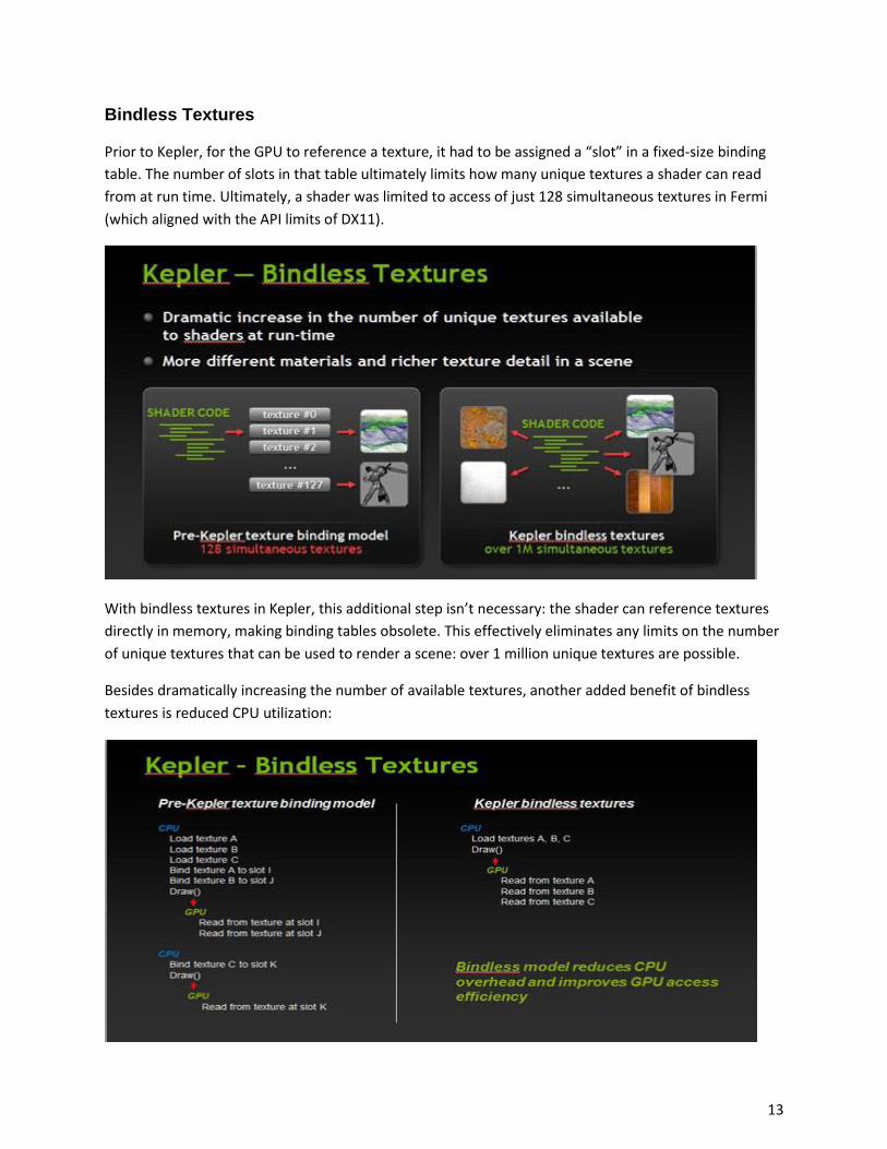
Bindless Textures
Prior to Kepler, for the GPU to reference a texture, it had to be assigned a “slot” in a fixed-size binding
table. The number of slots in that table ultimately limits how many unique textures a shader can read
from at run time. Ultimately, a shader was limited to access of just 128 simultaneous textures in Fermi
(which aligned with the API limits of DX11).
With bindless textures in Kepler, this additional step isn’t necessary: the shader can reference textures
directly in memory, making binding tables obsolete. This effectively eliminates any limits on the number
of unique textures that can be used to render a scene: over 1 million unique textures are possible.
Besides dramatically increasing the number of available textures, another added benefit of bindless
textures is reduced CPU utilization:

14
At this time, bindless textures is only exposed in OpenGL. But in the future it’s possible this could be
exposed in DirectX via NVAPI, or future versions of DirectX.
World’s Fastest GDDR5
For Kepler, the memory team developed a completely new IO design built to push to the theoretical
limits of GDDR5 signaling speed. In order to meet this ambitious goal, extensive improvements in circuit
and physical design, link training, and signal integrity were made based on in-depth study of our existing
silicon. The significant improvement in speed was only made possible by a highly integrated cross-
functional effort that enables the co-optimization of these three major areas of improvements. The
result was the industry’s first 6Gbps GDDR5 product.

15
GPU Boost
When determining the thermal design power (TDP) limit of our GPUs, NVIDIA engineers monitor the
GPU’s power consumption while running a wide range of real-world 3D applications in a worst-case
thermal environment. We then set the GPU’s clock speeds based on these results.
Under real world conditions running today’s latest games, however, most GPUs will never approach
their TDP; power consumption varies from one application to another, and most users don’t run their
GPUs under worst-case environmental conditions.
In cases where the GPU isn’t fully taxed, it would be beneficial if the GPU could increase its clock
frequency to deliver improved 3D performance and/or higher image quality with richer graphics effects
enabled. This is where NVIDIA’s GPU Boost technology comes in.
A combination of hardware and software technology that works with the GeForce GTX 680, GPU Boost
works in the background, dynamically adjusting the GPU’s graphics clock speed automatically, based on
GPU operating conditions. Dedicated hardware circuitry continually monitors GPU power consumption.
GPU Boost automatically adjusts clocks to achieve the maximum possible clock speed while remaining
within a predefined power target.
170W is the typical board power NVIDIA has defined for the GeForce GTX 680 and GPU Boost. Under
load, most cards will typically operate at this power level. After careful consideration, we ultimately
determined this power level delivers the optimal combination of GPU power, temps, and acoustics,
providing an exquisite experience for GeForce GTX 680 users.

16
GPU Boost operates completely autonomously with no game profiles and no intervention required by
the end user, providing an instant performance boost to gamers.
GeForce GTX 680’s base 3D frequency is 1006MHz, which is called the “Base Clock.” This is the minimum
3D frequency the GPU is guaranteed to achieve running under load in TDP apps (strenuous real-world
applications that push power utilization to the Thermal Design Power limits of a GPU).
The “Boost Clock” is the average clock frequency the GPU will run under load in many typical non-TDP
apps that require less GPU power consumption. On average, the typical Boost Clock provided by GPU
Boost in GeForce GTX 680 is 1058MHz, an improvement of just over 5%. The Boost Clock is a typical
clock level achieved while running a typical game in a typical environment.
However, in many cases the GPU will have additional power headroom available and will automatically
increase the Boost Clock even higher than 1058MHz. As long as the GPU remains under its power target,
GPU Boost will seamlessly increase the GPU Clock: clock speeds of 1.1GHz or higher have been observed
internally in testing various non-TDP apps.
GPU Boost is fully compatible with GPU overclocking. Using third-party overclocking utilities provided by
NVIDIA board partners, GeForce GTX 680 users can adjust the GPU’s power target to enable higher clock
speeds. Once the power target has been increased, the GPU can be overclocked by raising the GPU clock
offset. As you can see in the screenshot below, some GeForce GTX 680 cards are able to scale to much
higher clock speeds:
Figure 3: GeForce GTX 680 runs Heaven at over 1.2GHz with complete stability!

17
Adaptive VSync
Long ago, game content was rendered by presenting new frames synchronously with display refresh
intervals (aka Vertical sync.). However, this approach leads to noticeable stuttering or hitching effects
whenever the rendering rate drops below the refresh rate (typically 60Hz)—if the rendering rate is only
a little slower, the synchronization step will drop from 60Hz to 30Hz (and other multiples of 60, such as
20 or 15Hz), leading to stuttering.
To avoid this undesirable effect, one approach has been to run with VSync disabled. Instead, new frames
are presented immediately, with a “tear line” visible on the screen at the switch point between old and
new frames. This is a better approach at low frame rates, but when rendering is fast, the tearing
introduces an unnecessary and very noticeable visual artifact. Tearing can be visually distracting to the
end user, leading to a less enjoyable gaming experience. (Tearing can also occur when frame rates are
less than the refresh rate, but it’s more noticeable at higher fps.)

18
To tackle this challenge, NVIDIA software engineers have developed Adaptive VSync. NVIDIA’s Adaptive
VSync technology, introduced with our Release 300 drivers, dynamically varies VSync on and off to
display frames at a more regular cadence, minimizing stuttering in games.
When frame rates drop below 60 frames per second, NVIDIA Adaptive VSync technology automatically
disables VSync, allowing frame rates to run at their natural rate, effectively reducing stutter. Once frame
rates return to 60 fps, Adaptive VSync turns VSync back on to reduce tearing.
The end result is a smoother, more enjoyable gaming experience.

19
Adaptive VSync is a new feature shipping with our R300 drivers and is compatible with GeForce GTX 680
as well as prior generation GeForce GPUs. Adaptive VSync can be found within the Vertical sync setting
in the NVIDIA control panel:
Two Adaptive VSync options are available within the control panel: Adaptive and Adaptive (half refresh
rate).
The half refresh rate option is useful in situations where your performance is generally between 25 – 50
frames per second. In these cases, the half refresh rate setting will lock VSync at 30 when frame rates
are 30 fps or more, and dynamically turn VSync off as the frame rate goes below 30 fps for a smoother
experience with reduced stuttering.

20
FXAA
NVIDIA FXAA technology harnesses the power of the GPU’s CUDA Cores to reduce visible aliasing. FXAA
is a pixel shader-based image filter that is applied along with other post processing steps like motion
blur and bloom. For game engines making use of deferred shading, FXAA provides a performance and
memory advantage over deferred shading with multi-sample anti-aliasing (MSAA).
FXAA targets edge aliasing and also aliasing on single-pixel and sub-pixel sized features, which tend to
flicker as they move from frame to frame. FXAA reduces the visual contrast of these features so that
they are less jarring to the eye. Note that FXAA cannot completely solve the sub-pixel aliasing problem,
but it does substantially reduce it. The overall effect is smoother visual quality.
FXAA reduces but does not completely eliminate shader aliasing. FXAA’s chief advantage over traditional
MSAA is higher performance. In many cases, FXAA can be applied at a cost of 1ms per frame or less,
resulting in frame rates that are often 2x higher than 4xMSAA with comparable image quality.
NVIDIA FXAA was first implemented in games last year beginning with Age of Conan. Since then, FXAA
has shipped in 15 additional titles.
FXAA has been added to the driver control panel beginning with the release of our R300 drivers. With
FXAA support now built in to the graphics driver, FXAA can be enabled in hundreds of games.

21
Please note that there are multiple versions of FXAA:
Developer-integrated FXAA: Initial versions of FXAA (FXAA 1) shipped with games like Age of
Conan, F.E.A.R.3, and Duke Nukem Forever. It was designed to provide high visual quality, at the
cost of slower performance. The most current version of FXAA (FXAA 3) is available for game
developers to integrate into their game engines as a drop-in AA solution. It provides a more
optimal combination of performance and image quality than the original version of FXAA and it
works across DX9 through DX11 and OpenGL. It has a configurable performance, quality, and
sharpness tradeoff that will vary from title to title depending on what choices the developer
makes during integration. FXAA 3 is used in Battlefield 3.
Control-panel FXAA: This is the version used in the R300 driver control panel. It is a mixture of
FXAA 1 and FXAA 3 with some modifications to look better than FXAA 1 on text. In comparison
to FXAA 3 integrated into games, control-panel FXAA will provide better image quality except for
the HUD and text, since it is applied after they are rendered in the graphics pipeline. This version
of FXAA also performs slower than FXAA 3.
As you can see, over the last year FXAA has evolved to become a popular AA option for game developers
who need a high performance AA solution that can be tweaked to their specific game engine needs.
Gamers benefit because they can play their favorite games with high image quality without paying the
performance tax of MSAA; and now that we’re providing a driver-based FXAA option that’s built-in to
the control panel, gamers can experience the benefits of FXAA firsthand in most of their games.
NOTE: If you would like to take screenshots of our control panel-based FXAA while in-game, you will need to press the Print Screen button. FRAPS isn’t able to capture screenshots that accurately reflect our driver-based control panel FXAA.

22
At the Game Developers Conference in San Francisco last year, Epic demonstrated their Samaritan
demo, providing a sneak peak at what next-generation DX11 games may look like. Running on three
GeForce GTX 580 GPUs in 3-Way SLI configuration, the Samaritan demo stunned the crowd with its DX11
tessellation and displacement mapping, subsurface scattering, depth of field, reflections, dynamic
shadows, and more.
Utilizing the power of the Kepler architecture and NVIDIA FXAA technology, one year later that same
demo can now be run on one GeForce GTX 680 GPU!

23
TXAA
TXAA is a new film-style AA technique that is designed to exploit GeForce GTX 680’s high FP16 texture
performance. TXAA is a mix of hardware anti-aliasing, custom CG film style AA resolve, and in the case of
2xTXAA, an optional temporal component for better image quality. The bulk of TXAA is a high-quality
resolve filter, which is carefully designed to work with the HDR-correct post processing pipeline.

24
TXAA is available with two modes: TXAA 1, and TXAA 2. TXAA 1 offers visual quality on par with 8xMSAA
with the performance hit of 2xMSAA, while TXAA 2 offers image quality that is superior to 8xMSAA, but
with performance comparable to 4xMSAA.
25
Like our FXAA technology, TXAA will first be implemented in upcoming game titles shipping later this
year.
The following games and game engines/developers have committed to offering TXAA support so far: MechWarrior Online, Secret World, Eve Online, Borderlands 2, Unreal 4 Engine, BitSquid, Slant Six Games, and Crytek.

26
New Display/Video Engine
All Kepler GPUs feature an all-new display engine that has been tailored for next-generation 4k and
3GHz HDMI displays, multi-display gaming with NVIDIA Surround, multi-stream audio, and enhanced
video transcoding.
GeForce GTX 680’s display engine is capable of driving up to four displays simultaneously, and provides
native Surround support from one GeForce GTX 680 card.
Figure 4: GeForce GTX 680 natively supports up to 4 display gaming
The GeForce GTX 680 reference board design ships with two dual-link DVI connectors, as well as HDMI
and DisplayPort outputs. Based on NVIDIA research, DVI is still the most common display output. And
with full-size HDMI and DisplayPort connections, no adapters are needed to support most displays on
the market.
NVENC
All Kepler GPUs also incorporate a new hardware-based H.264 video encoder, NVENC.
Prior to the introduction of Kepler, video encoding on previous GeForce products was handled by
encode software running on the GPU’s array of CUDA Cores. While the CUDA Cores were able to deliver
tremendous performance speedups compared to CPU-based encoding, one downside of using these
high-speed processor cores to process video encoding was increased power consumption.
By using specialized circuitry for H.264 encoding, the NVENC hardware encoder in Kepler is almost four
times faster than our previous CUDA-based encoder while consuming much less power.

27
It is important to note that an application can choose to encode using both NVENC hardware and
NVIDIA’s legacy CUDA encoder in parallel, without negatively affecting each other. However, some video
pre-processing algorithms may require CUDA, and this will result in reduced performance from the
CUDA encoder since the available CUDA Cores will be shared by the encoder and pre-processor.
NVENC provides the following:
Can encode full HD resolution (1080p) videos up to 8x faster than real-time. For example, in high
performance mode, encoding of a 16 minute long 1080p, 30 fps video will take approximately 2
minutes.
Support for H.264 Base, Main, and High Profile Level 4.1 (same as Blu-ray standard)
Supports MVC (Multiview Video Coding) for stereoscopic video—an extension of H.264 which is
used for Blu-ray 3D.
Up to 4096x4096 encode
We currently expose NVENC through proprietary APIs, and provide an SDK for development using
NVENC. Later this year, CUDA developers will also be able to use the high performance NVENC video
encoder. For example, you could use the compute engines for video pre-processing and then do the
actual H.264 encoding in NVENC. Alternatively, you can choose to improve overall video encoding
performance by running simultaneous parallel encoders in CUDA and NVENC, without affecting each
other’s performance.
NVENC enables a wide range of new use cases for consumers:
HD videoconferencing on mainstream notebooks
Sending the contents of the desktop to the big screen TV (gaming, video) through a wireless
connection
Authoring high quality Blu-ray discs from your HD camcorder
A beta version of Cyberlink MediaEspresso with NVENC support is now available on the GeForce GTX
680 press FTP. Support will be coming soon for Cyberlink PowerDirector and Arcsoft MediaConverter.

28
Conclusion
Through a combination of hardware and software advancements, GeForce GTX 680 has been crafted to
provide PC gamers with a delightful gaming experience.
GeForce GTX 680’s new SMX unit features a number of architecture changes that allow it to deliver
unparalleled levels of performance and power efficiency. In order to reduce power consumption while
still improving GPU performance, we have eliminated the shader clock and significantly increased the
number of CUDA Cores, Special Function Units, and texture units. In addition, the SMX PolyMorph
Engine has been redesigned to deliver roughly double the performance of the unit used in Fermi. To
improve performance even further, GeForce GTX 680 also features new GPU Boost technology that
automatically increases the graphics clock speed to maximize frame rate in games.
GeForce GTX 680 supports a number of new features that have been designed to deliver a smoother
experience for gamers. NVIDIA Adaptive VSync technology dynamically turns VSync on and off as
needed for reduced tearing and stutter. NVIDIA FXAA technology—already a hit with gamers—is now
coming to the GeForce GTX 680’s driver control panel. Lastly, TXAA, an upcoming AA technique
developed by NVIDIA, brings greater than 8xMSAA image quality at the performance cost of 4xMSAA.
Offering built-in support for up to four displays, one GeForce GTX 680 card natively supports 3D Vision
Surround. GeForce GTX 680 also features a new hardware-based H.264 video encoder, NVENC. NVENC is
almost four times faster than our previous CUDA-based encoder while consuming much less power.
With its new SMX architecture and increased clock speeds provided by GPU Boost, the GeForce GTX 680
delivers breakthrough levels of performance and power efficiency. With advancements like Adaptive
VSync, FXAA, and TXAA, games have never looked and run smoother. And the ability to run 3D Vision
Surround on a single GTX 680 provides gamers with a richer experience.
The GeForce GTX 680 is the “must-have” GPU for enthusiast gamers today. It’s the fastest, most efficient
GPU ever built.

29
Notice ALL INFORMATION PROVIDED IN THIS WHITE PAPER, INCLUDING COMMENTARY, OPINION, NVIDIA DESIGN SPECIFICATIONS, REFERENCE BOARDS, FILES, DRAWINGS, DIAGNOSTICS, LISTS, AND OTHER DOCUMENTS (TOGETHER AND SEPARATELY, “MATERIALS”) ARE BEING PROVIDED “AS IS.” NVIDIA MAKES NO WARRANTIES, EXPRESSED, IMPLIED, STATUTORY, OR OTHERWISE WITH RESPECT TO MATERIALS, AND EXPRESSLY DISCLAIMS ALL IMPLIED WARRANTIES OF NONINFRINGEMENT, MERCHANTABILITY, AND FITNESS FOR A PARTICULAR PURPOSE. Information furnished is believed to be accurate and reliable. However, NVIDIA Corporation assumes no responsibility for the consequences of use of such information or for any infringement of patents or other rights of third parties that may result from its use. No license is granted by implication or otherwise under any patent or patent rights of NVIDIA Corporation. Specifications mentioned in this publication are subject to change without notice. This publication supersedes and replaces all information previously supplied. NVIDIA Corporation products are not authorized for use as critical components in life support devices or systems without express written approval of NVIDIA Corporation. Trademarks NVIDIA, the NVIDIA logo, CUDA, FERMI, KEPLER and GeForce are trademarks or registered trademarks of NVIDIA Corporation in the United States and other countries. Other company and product names may be trademarks of the respective companies with which they are associated. Copyright © 2012 NVIDIA Corporation. All rights reserved.