gsfc preferred parts list ppl-17 - ntrs.nasa.gov
TRANSCRIPT
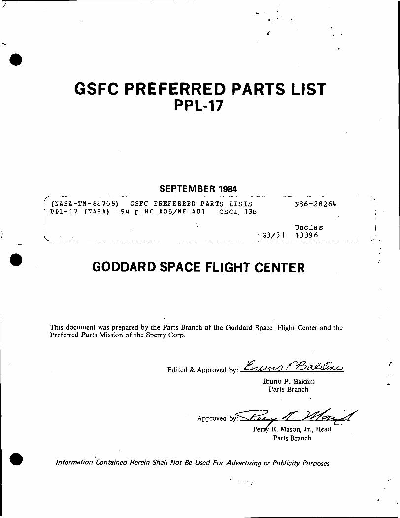
GSFC PREFERRED PARTS LISTPPL-17
SEPTEMBER 1984
I N A S A - T M - 8 8 7 6 S ) GSFC PBEFEBEED PABTS.LISTS N86-28264PPL-17 ( N A S A ) .94 p HC. A05/HF A01 CSCL. 13B
v :..._:Duclas
G3/31 43396
GODDARD SPACE FLIGHT CENTER
This document was prepared by the Parts Branch of the Goddard Space Flight Center and thePreferred Parts Mission of the Sperry Corp.
Edited & Approved by: _i=si
Bruno P. BaldiniParts Branch
Approved ^ v - ^ r * , x r ^/
Perny R. Mason, Jr., HeadParts Branch
Information Contained Herein Shall Not Be Used For Advertising or Publicity Purposes

PREFACE
PURPOSE
This document contains a listing of preferred parts, part upgrading procedures, part deratingguidelines, and part screening procedures to be used in the selection, procurement, and applicationof parts for GSFC space systems and ground support equipment.
AUTHORITY
The GSFC PPL is authorized and invoked by Goddard Management Instructions (GMI)5330.6, Implementation of the Goddard Space Flight Center Parts Program.
STANDARDIZATION
MIL-STD-975, the NASA Standard (EEE) Parts List (NSPL), is the prime referencedocument for preferred electronic parts for NASA. The GSFC Preferred Parts List (PPL-17),complements MIL-STD-975 by listing additional part types and part categories not included inMIL-STD-975. Parts or styles listed in MIL-STD-975 are identified in PPL-17 as a convenience tousers. Several part types listed in MIL-STD-975 are not identified in PPL-17. They are consideredto be nonstandard, and are so noted in the PPL. Where conflicts exist between the NSPL andPPL-17, PPL-17 takes precedence.
All parts not specifically identified in the current issues of MIL-STD-975 or the GSFC PPLor which are not procured to the specification given in MIL-STD 975 or PPL are non-standard.These parts shall be used only, with the approval of the GSFC Project Office, if needs cannot besatisfied with a standard part.
QUALITY LEVELS
Consistent with MIL-STD-975, PPL-17 specifies two levels of quality. Grade 1 parts are higherquality, government-specification-controlled parts intended for critical applications. Grade 2 partsare high quality government-specification-controlled parts for use in applications where grade 1parts are not required.
The parts listed in this document meet the requirements of a Military or NASA specification.When a PPL listed part is purchased, the specification listed for the part and the recommendedmanufacturer(s) or the manufacturers on the QPL for the part must be referenced in theprocurement request.
All specifications listed in the PPL are maintained on file in the Parts Branch for referencepurposes. GSFC personnel can obtain copies of specifications through their division offices fromthe Parts Branch Library, code 310.1, telephone (301) 344-7240. Contractors, approved domesticand foreign experimenters, and international cooperative project working groups can obtain copies
111PRECEDING P&GE BLANK WV FILLED

of the PPL and copies of referenced documents, except MIL specifications, by a written requestvia the cognizant project office. All others may obtain copies of the PPL through the NationalTechnical Information Service (NTIS), Springfield, VA 22161 or the GIDEP data bank. Requestsfor Military Specifications should be directed to:
Commanding OfficerNaval Publications and Forms Center, Code 30155801 Tabor AvenuePhiladelphia, PA 19120
REVISIONS
The PPL will be reissued during 1986. Portions may be changed and updated prior to thatdate, as required. Parts not now listed, for which a substantial or critical usage is anticipated,should be brought to the attention of the Parts Branch so that those parts may be considered ascandidates for evaluation and possible future listing in MIL-STD-975 or the GSFC PPL. Call(301) 344-8923 or (301) 344-6485.
PART CHARACTERISTICS
Electrical characteristics are specified at 25°C ambient, unless otherwise noted.
CRITERIA FOR LISTING PARTS
Parts are listed in the PPL based on the following criteria:(1) they can be procured to a high reliability military or NASA specification;(2) they have complied with an approved series of qualifying criteria;(3) they are judged by the GSFC Parts Branch to be available and not redundant to other
parts in the GSFC PPL or MIL-STD-975.
USER RESPONSIBILITY
MIL-STD-975 and the PPL serve the Center covering both Flight and Ground SupportEquipment applications and needs. It is the responsibility of the user, the product assuranceengineer, and flight assurance manager to insure that the proper grade level parts are selectedfrom MIL-STD-975 and the PPL commensurate with the criticality of the application.
IV

PARTS APPLICATIONS
MIL-HDBK-978, NASA Parts Application Handbook, is intended to maintain a partstechnology baseline for NASA centers and NASA contractors and to maximize standard partsusage. It is an integral part of the NASA standard parts program.
Those part categories covered in MIL-HDBK-978 that are also found in PPL-17 are:Microcircuits (Microelectronic Devices), Transistors, Diodes, Capacitors, Resistors, Connectors,Filters, Protective Devices, Relays, Transformers and Inductors. Some other features found in thehandbook are: Cost Factors, Definitions, Construction Details, Operating Characteristics, FailureMechanisms, Screening Techniques, Environmental Considerations, Selection Criteria, CircuitApplication, Failure Rates and Radiation Effects.
PARTS UPGRADING
For some types of parts listed in MIL-STD-975 and the PPL, Grade 1 parts are not listed.Appendix A gives guidelines for upgrading a Grade 2 part for use in a Grade 1 application. In allcases, upgrading must be approved by submission of a non-standard part approval rquest. Thisadditional testing does not provide a part that is equivalent to the Grade 1 part. Subsequenttesting never can duplicate design and processing controls that are imposed during manufacturing.
PARTS DERATING
Conservative application stresses are an important design tool for decreasing part degrada-tion, improving failure rates, and prolonging the useful life of parts. For guidance, recommendedpart derating factors are tabulated in Appendix B.
PARTS SCREENING
Screening is designed to eliminate quality defects that will prevent a part from meeting itsintended performance requirements. Screening is not a substitute for the design and processingcontrols that can be applied to a part during manufacturing to improve its reliability. Appendix Cgives screening guidelines that should be used when a nonstandard part must be procured becauseno standard part is available.
PARTS RADIATION EFFECTS
Space radiation can present a hazard to electronic parts on space missions. Appendix D givesinformation on radiation effects on electronic parts.
REFERENCED SPECIFICATIONS
Unless noted otherwise, all specifications referenced in the PPL are the issue in effect on thedate of PPL issue.

PARTS INFORMATION DIRECTORY
Assistance in the selection of parts, parts specifications, manufacturers surveys, incominginspection, screening evaluation tests and failure analysis services for all parts are available from theParts Branch of the Product Assurance Division.
For assistance on electronic parts problems and questions in direct support of specific projects,users should contact the cognizant parts specialist assigned to the respective project. If unknown,the identity can be determined by contacting the project office.
For general evaluation information of electronic parts, part specifications, and part qualifi-cations, users may contact a specialist in the particular part category, as listed below:
PART CATEGORY SPECIALIST . TELEPHONE(301) 344-
Capacitors P. Jones 5910Connectors J. Lawrence 5640Crystals V. Patel 6382Diodes M. Robertson 5910Electro Optics L. Milliard 5987Filters V. Patel 6382Fuses J. Henegar 5345Inductors F. Kreis 7339Microcircuits S. Bryant 7437PC Boards j H. Chernikoff 5984
|F. Kreis 7339Relays J. Lawrence 5640Resistors F. Kreis 7339Thermistors J. Henegar 5345Transformers F. Kreis 7339Transistors M. Robertson 5910Wire and Cable J. Lawrence 5640All Preferred Parts J6588
J6220
Additional services in support of the GSFC parts program are:
FUNCTION CONTACT TELEPHONE(301) 344-
Electronic Parts Qualification 1 _ _ ... . „_,„T ,. ., . , - ,. nnT B. Baldim 8923Testing, Maintenance of the PPL)Electronic Parts Incoming Test,) w Owens 6134
Inspection, and Screening IData Systems G. Ritter 7635Failure Analysisn . .. TO. , A , • i B. Baldini 8923Destructive Physical Analysis)
VI

FUNCTION CONTACT TELEPHONE(301)344-
„ . . D c • r * IH- Chernikoff 5984Packaging Process Specialist <p .
D ,. .. crp . (J. Adolphsen 8896Radiation Effects J „. _. F. , _ .,_D. Cleveland 7437
vn
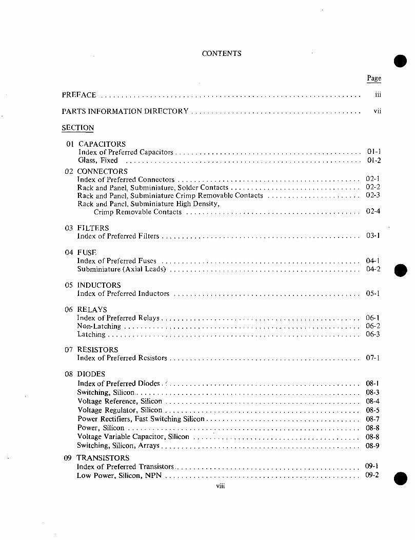
CONTENTS
Page
PREFACE iii
PARTS INFORMATION DIRECTORY vii
SECTION
01 CAPACITORSIndex of Preferred Capacitors 01-1Glass, Fixed 01-2
02 CONNECTORSIndex of Preferred Connectors 02-1Rack and Panel, Subminiature, Solder Contacts 02-2Rack and Panel, Subminiature Crimp Removable Contacts 02-3Rack and Panel, Subminiature High Density,
Crimp Removable Contacts 02-4
03 FILTERSIndex of Preferred Filters 03-1
04 FUSEIndex of Preferred Fuses 04-1Subminiature (Axial Leads) , 04-2
05 INDUCTORSIndex of Preferred Inductors 05-1
06 RELAYSIndex of Preferred Relays 06-1Non-Latching 06-2Latching 06-3
07 RESISTORSIndex of Preferred Resistors 07-1
08 DIODESIndex of Preferred Diodes . 08-1Switching, Silicon 08-3Voltage Reference, Silicon 08-4Voltage Regulator, Silicon 08-5Power Rectifiers, Fast Switching Silicon 08-7Power, Silicon 08-8Voltage Variable Capacitor, Silicon 08-8Switching, Silicon, Arrays 08-9
09 TRANSISTORSIndex of Preferred Transistors 09-1Low Power, Silicon, NPN 09-2
viii

SECTION
CONTENTS (cont.)
Page
09 (cont.)Low Power, Silicon, PNP 09-2Medium Power, Silicon, PNP 09-2Medium Power, Silicon, NPN 09-3Chopper, Low Power, Silicon, PNP 09-3High Power, Silicon, NPN 09-4High Power, Silicon, PNP 09-4Field Effect, N—Channel, Junction, Silicon 09-5
10 MICROCIRCUITSIndex to Preferred Microcircuits 10-1Microcircuit Information 10-3Digital, MIL-M-38510 Advanced Low Power Schott Ky TTL 10-4Digital, MIL-M--38510 CMOS 10-5
14 THERMISTORSIndex of Preferred Thermistors 14-1Negative Temperature Coefficient 14-2
15 TRANSFORMERSIndex of Preferred Transformers 15-1
16 WIRE AND CABLEIndex of Preferred Wire and Cable 16-1Electrical, Insulated, High Temperature 16-2Electrical, Insulated, Lightweight 16-3Electrical, Insulated -. 16-6Color Code Designators for Wire According to MIL-STD-681 16-7
APPENDIX A - Upgrading Grade 2 Devices for Use inGrade 1 Applications A-l
— Upgrading Guidelines A-2
APPENDIX B — Parts Derating Factors B-l
APPENDIX C — Screening of Non-Standard Parts C-l
APPENDIX D — Radiation Effects D-l
APPENDIX E — Screening Verification E-l
IX

Index of Preferred Capacitors
Style
CCR
CDR
CKR2
CLR3. i
CRH
CSR5.6
CWR
CYR
Description
Ceramic, Temperature-compensating, Fixed
Ceramic, Chip, Multiple-layered, Fixed
Styles CDR01, 03, 04, 05, 06
Ceramic, Fixed
Tantalum (non-solid) electrolytic. Fixed
Plastic (metalized), Fixed
Tantalum (solid) electrolytic, Fixed
Tantalum Chip, Fixed
Glass, Fixed
Styles CYR 10, 15, 20, 30
Styles CYR13, 41, 42, 43, 51, 52, 53
Specification
MIL-C-20
MIL-C-55681
MIL-C-39014
MIL-C-39006
MIL-C-83421
MIL-C-39003
MIL-C-55365
MIL-C-23269
Refer To
MIL-STD-975
MIL-STD-975
MIL-STD-975
MIL-STD-975
MIL-STD-975
MIL-STD-975
MIL-STD-975
MIL-STD-975
Pages 01-2 to 01-7
NOTES:1. CKR styles are to be limited to maximum capacitance values as follows:
CKR05- 33,000 pf CKR11- 4,700 pf CKR14- 47,000 pfCKR06-333,000 pf CKR12- 10,000 pf CKR15- 180,000 pfCKR styles shall be purchased to revision C of MIL-C-39014.
2. CLR styles with ratings above 100 volts are not to be used for Grade I applications.
3. A non-standard parts approval is needed if the requirements of notes 1 and 2 are to be waived.
4. The CLR79 style wet slug tantalum capacitors shall be subjected to an acid indicator leak test in accordance withparagraphs III and IV of GSFC screening procedure SP01.23.
5. EFFECTIVE SERIES RESISTANCE SEEN BY CSR STYLE CAPACITORS SHOULD BE EQUAL TO OR GREATERTHAN ONE OHM/VOLT. AS NOTED IN MIL-STD-975, THE CSR STYLE OF CAPACITOR IS NOTRECOMMENDED FOR USE IN APPLICATIONS OF LESS THAN ONE OHM/VOLT, AS IN POWER SUPPLY FILTERS.
6. Surge current testing shall be performed on CSR style capacitors for all Grade 1 applications per MIL-STD-975.
01-1 PPL 17September, 1984

MIL-C-23269, CAPACITORSFixed, Glass Dielectric, Established Reliability
Part Number example:
ParrNumber
M23269/05
M23269/09
Style
CYR13
CYR41CYR42CYR43
M23269 /XX XXXX
M-Number - identifies "CYR" fixed, glass /XX - identifies the appropriate military specification XXXX - uniquely specifies the nominal capacitancedielectric, established reliability capacitors sheet that uniquely specifies the capacitor family. value, capacitance tolerance, rated dc voltage, andconforming to MIL-C-23269. failure rate level (%/1000 hours).
SeePage01-
3,4
567
CapacitanceRange
(pF)
0.5-300
0.5-10000.5-300330-1200
MaximumDissipation
Factor(%)
0 7 0 3 0 1
0.1
RatedVoltage
(volts, dc)
300, 500
10050-50050-300
Temperature
Range°C
-55° Cto
+125°C
Coefficient(ppm/°C)
105 ±25
0±25
MinimumInsulationResistance(megohms)
500 K@25°C
Configuration
CaseType
Rectangular,hermetic
LeadType
Axial orRadial
RadialAxialAxial
Grade 1FRL
R
(Note 1)
Grade 2FRL
P
P
Manufacturer
QPL-23269
NOTES:1. No Grade 1 parts are available at the present time.
01-2 PPL 17September, 1984

M23269/05, STYLE CYR13Fixed, Glass Dielectric, Established Reliability
Capacitance
Value(pF)
0.51 .01.52.2
2.73.0
3.33.6
3.94.3
4.75.15.6
6.2
6.8
7.5
8.2
9.1
10
11
Tolerance(±)
0.25pF0.25pF0.25pF0.25pFO.SOpF0.25pF0.25pFO.SOpF0.25pF0.25pFO.SOpF0.25pF0.25pFO.SOpF0.25pF0.25pF0.25pF
5%0.25pF
5%0.25pF
5%0.25PF
5%0.25pF
5%0.25pF
5%0.25pF
5%0.25pF
5%
DissipationFactor
(%)
0.7
0.3
RatedVoltage
(volts, dc)
500
Part Number M23269/05-
Grade 1FRL=R(0.01)
50015002500350045005500650075008500950105011501250135014501550165017501850195020502150225023502450255026502750285029503050315032
Grade 2FRL = P(0.1)
40014002400340044005400640074008400940104011401240134014401540164017401840194020402140224023402440254026402740284029403040314032
Capacitance
Value(pF)
12
13
15
16
18
20
22
24
27
30
33
36
39
43
Tolerance
(±)
0.25pF5%2%5%2%5%2%5%2%5%2%5%2%5%2%5%1%2%5%1%2%5%1%2%5%1%2%5%1%2%5%1%
DissipationFactor(%)
0.3
0.1
RatedVoltage
(volts, dc)
500
Part Number M23269/05-
Grade 1FRL = R(0.01)
50335034503550365037503850395040504150425043504450455046504750485049505050515052505350545055505650575058505950605061506250635064
Grade 2FRL = P(0.1)
40334034403540364037403840394040404140424043404440454046404740484049405040514052405340544055405640574058405940604061406240634064
01-3 PPL 17September, 1984

M23269/05, STYLE CYR13 (continued)Fixed, Glass Dielectric, Established Reliability
Capacitance
Value(PF)
43
47
51
56
62
68
75
82
91
100
110
Tolerance
(± %)
2512512512512512512512512512512
DissipationFactor(%)
0.1
RatedVoltage
(volts, dc)
500
Part Number M23269/05-
Grade 1FRL= R(0.01)
5065506650675068506950705071507250735074507550765077507850795080508150825083508450855086508750885089509050915092509350945095
1 Grade 2FRL = P(0.l)
4065406640674068406940704071407240734074407540764077407840794080408140824083408440854086408740884089409040914092409340944095
Capacitance
Value(pF)
110
120
130
150
160
180
200
220
240
270
300
Tolerance(± %)
5125125125125125125125125125125
DissipationFactor(%)
0.1
RatedVoltage
(volts, dc)
500
300
Part Number M23269/05-
Grade 1FRL = R(0.01)
5096509750985099510051015102510351045105510651075108510951105111511251135114511551165117511851195120512151225123512451255126
Grade 2FRL=P(0.l)
4096409740984099410041014102410341044105410641074108410941104111411241134114411541164117411841194120412141224123412441254126
01-4 PPL 17September, 1984

M23269/09, STYLE CYR41Fixed, Glass Dielectric, Established Reliability
Capacitance
Value(pF)
0.51.52.73.33.94.75.66.8
8.2
10
12
15
18
22
27
33
39
47
56
68
Tolerance(±)
r 0.25pF0.25pF0.25pF0.25Pf0.25pF0.25pF0.25pF0.25Pf
5%0.25pF
5%0.25pF
5%0.25pF
5%0.25pF
2%5%
0.25pF2%5%
0.25pF2%
I 5%1%2%5%1%2%5%1%2%5%1%2%5%1%2%5%1%2%5%
DissipationFactor(%)
0.5
0.3
0.1
RatedVoltage
(volts, dc)
100
Part Number M23269/09-
Grade 2FRL=P(0.1)
400140024003400440054006400740084009401040114012401340144015401640174018401940204021402240234024402540264027402840294030403140324033403440354036403740384039404040414042
Capacitance
Value(pF)
82
100
120
150
180
220
270
330
390
470
560
680
820
1000
Tolerance
(± %)
125125125125125125125125125125125125125125
DissipationFactor(%)
0.1
RatedVoltage
(volts, dc)
100
Part Number M23269/09-
Grade 2FRL=P(0.1)
404340444045404640474048404940504051405240534054405540564057405840594060406140624063406440654066406740684069407040714072407340744075407640774078407940804081408240834084
01-5 PPL 17September, 1984

M23269/09, STYLE CYR42Fixed, Glass Dielectric, Established Reliability
Capacitance
Value(PF)
0.5I .52.73.33.94.75.66.8
8.2
10
12
15
18
22
27
33
39
Tolerance(±)
u_ u_ u_ u_ u_ LL.Q
_ Q
_ Q
_ Q
_ Q
_
aIT
) IT
) U
O IO
U
"> IO
CM
CM
CM
CM
CM
CM
O O
0 0 O
0
0.25pF0.25pF
5%0.25pF
5%0.25pF
5%0.25pF
5%0.25pF
2%5%
0.25pF2%5%
0.25pF2%5%1%2%5%1%2%5%1%2%5%
DissipationFactor
(%)
0.7
0.3
/
0.1
RatedVoltage
(volts, dc)
500
Part Number M23269/09-
Grade 2FRL=P(0.1)
410141024103410441054106410741084109411041114112411341144115411641174118411941204121412241234124412541264127412841294130413141324133
Capacitance
Value(PF)
47
56
68
82
100
120
150
180
220
270
300
Tolerance(± %)
125125125125125125125125125125125
DissipationFactor
(%)
0.1
RatedVoltage
(volts, dc)
500
300
100
50
Part Number M23269/09-
Grade 2FRL=P(0.1)
413441354136413741384139414041414142414341444145414641474148414941504151415241534154415541564157415841594160416141624163416441654166
01-6 PPL 17September, 1984

M23269/09, STYLE CYR431
Fixed, Glass Dielectric, Established Reliability
Capacitance
Value(PF)
330
390
470
560
680
Tolerance(± %)
I
2
5
1
2
5
1
2
5
1
2
5
1
2
5
RatedVoltage
(volts, dc)
100
Part Number M23269/09-
Grade 2FRL=P(0.1)
4301
4302
4303
4304
4305
4306
4307
4308
4309
4310
4311
4312
4313
4314
4315
Capacitance
Value(PF)
820
1000
1200
Tolerance(± %)
1
2
5
1
2
5
1
2
5
RatedVoltage
(volts, dc)
50
Part Number M23269/09-
Grade 2FRL=P(0.1)
4316
4317
4318
4319
4320
4321
4322
4323
4324
NOTE:1. Dissipation factor 0.1%
01-7 PPL 17September, 1984

Index of Preferred Connectors
Style
G311P10
311P409
311P407
NLS
NB
NBS
Description
Power Connectors, Solder Contacts (sub-miniature)
Power Connectors, Crimp Removable Contacts (sub-miniature)
Power connectors, Crimp Removable Contacts(sub-miniature High Density)
High Density, Miniature
Miniature (200°C)
Electrical, Miniature, Circular (200°C)
Specification
GSFC S-311-P-10
GSFC S-311-P-4/9
GSFCS311P-4/7
MSFC 40 M38277
MSFC40 M39569
MSFC 40 M38298
Refer To
Page 02-2
Page 02-3
Page 02-4
MIL-STD-975
MIL-STD-975
MIL-STD-975
NOTES:1. OTHER PARTS ARE LISTED IN MIL-STD-975, BUT GSFC CONSIDERS ONLY THE ONES LISTED ABOVE AS
STANDARD PARTS.
02-1 PPL 17September, 1984

RackPOWER CONNECTORS
and Panel, Sub-Miniature, Solder Contacts
Construction
Receptacle,Rectangular
Plug,Rectangular
Contacts
Qty.
9
15
25
37
50
9
15
25
37
50
Type
Socket
Socket
Socket
Socket
Socket
Pin
Pin
Pin
Pin
Pin
For Use WithWire Size
AWG #20 maxr\il\J £.\J II1UA •
Grade 1 & Grade 2
GSFC Type1
G311P10B-1S-C-15
G311P10B-2S-C-15
G311P10B-3S-C-15
G311P10B-4S-C-15
G311P10B-5S-C-15
G311P10-1P-C-15
G311P10-2P-C-15
G311P10-3P-C-15
G311P10-4P-C-15
G311P10-5P-C-15
SpecificationGSFC
S-31 i-p-io
Manufacturer
ITT CannonElectric
TRW CinchConnectors
Remarks
All GSFC type connectors:"-15" in type indicates 0.154 inch(0.39 mm) dia. mounting hole,0.120 inch (0.31 mm) dia. isavailable; indicated by "-12."
NOTES:1. C = 20 gamma residual magnetism level; other levels B = 200 and 0 = 2 gamma are available.
02-2 PPL 17September, 1984
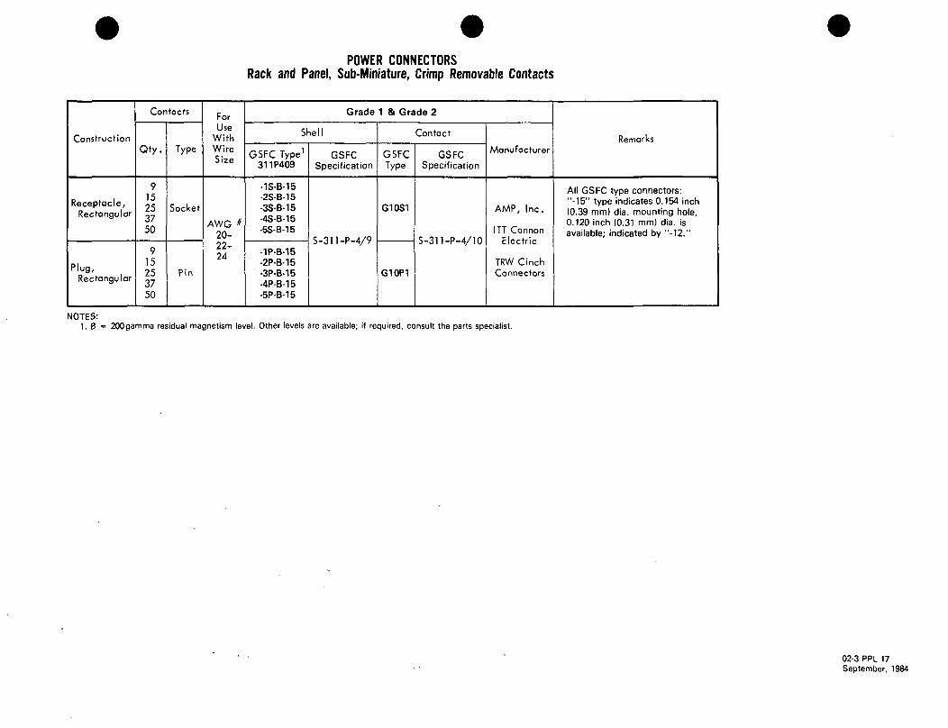
POWER CONNECTORSRack and Panel, Sub-Miniature, Crimp Removable Contacts
Construction
Receptacle,Rectangular
Plug,Rectangular
Contacts
Qry.
915253750
915253750
Type
Socket
Pin
ForUse
WithWire<;;•».=
AWG #20-22-94
Grade 1 & Grade 2
Shell
GSFC Type1
311P409
•1S-B-15-2S-B-15-3S-B-15-4S-B-15-5S-B-15
-1P-B-15-2P-B-15-3P-B-15-4P-B-15-5P-B-15
GSFCSpecification
S-311-P-4/9
Contact
GSFCType
G10S1
G10P1
GSFCSpecification
S-311-P-4/10
Manufacturer
AMP, Inc.
ITT CannonElectric
TRW CinchConnectors
Remarks
All GSFC type connectors:"-15" type indicates 0.154 inch(0.39 mm) dia. mounting hole,0.120 inch (0.31 mm) dia. isavailable; indicated by "-12."
NOTES:1. 8 - 200gamma residual magnetism level. Other levels are available; if required, consult the parts specialist.
02-3 PPL 17September, 1984

POWER CONNECTORSRack and Panel, Sub-Miniature, High Density, Crimp Removable Contacts
Construction
Receptacle,Rectangular
Plug,Rectangular
Contacts
Qty.
1526446278
104
1526446278
104
Type
Socket
Pin
ForUse
WithWirec;7e
AWG #
22-24-26-28
Grade 1 & Grade 2
Shell
GSFC Type'1
311P407
-1S-B-15-2S-B-15-3S-B-15-4S-B-15-5S-B-15-6S-B-15
-1P-B-15-2P-B-15-3P-B-15-4P-B-15-5P-B-15-6P-B-15
SpecificationGSFC
S-3H-P-4/7
Contact
GSFCType
G08S1
G08P1
SpecificationGSFC
S-3H-P-4/8
Manufacturer
Amp, Inc.
Remarks
All GSFC type connectors:"-15" type indicates 0.154 inch(0.39 mm) dia. mounting hole,0.120 inch (0.31 mm) dia. isavailable; indicated by "-12."
NOTES:1. B = 200 gamma residual magnetism level. No other residual magnetism levels are available for this type of connector.
02-4 PPL 17September, 1984
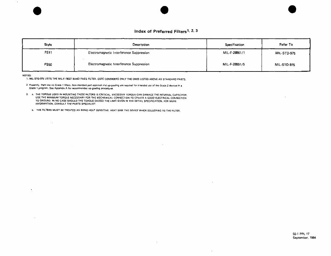
Index of Preferred Filters1- 2- 3
Style
FS11
FS50
Description
Electromagnetic Interference Suppression
Electromagnetic Interference Suppression
Specification
MIL-F-28861/1
MIL-F-28861/5
Refer To
MIL-STD-975
MIL-STD-975
NOTES:1. MIL-STD-975 LISTS THE MIL-F-18327 BAND PASS FILTER. GSFC CONSIDERS ONLY THE ONES LISTED ABOVE AS STANDARD PARTS.
2. Presently, there are no Grade 1 filters. Non-standard part approval and up-grading are required for intended use of the Grade 2 devices in aGrade 1 program. See Appendix A for recommended up-grading procedures.
3. a. THE TORQUE USED IN MOUNTING THESE FILTERS IS CRITICAL. EXCESSIVE TORQUE CAN DAMAGE THE INTERNAL CAPACITOR.USE THE MINIMUM TORQUE NECESSARY FOR THE MECHANICAL CONNECTION TO CREATE A GOOD ELECTRICAL CONNECTIONTO GROUND. IN NO CASE SHOULD THE TORQUE EXCEED THE LIMIT GIVEN IN THE DETAIL SPECIFICATION. FOR MOREINFORMATION, CONSULT THE PARTS SPECIALIST.
b. THE FILTERS MUST BE TREATED AS BEING HEAT SENSITIVE. HEAT SINK THE DEVICE WHEN SOLDERING TO THE FILTER.
03-1 PPL 17September, 1984

Index Of Preferred Fuses
Style Description Specification Refer To
FM04A
FM08A
Fuse, Subminiature
Fuse, Subminiature
MIL-F-23419
MIL-F-23419
Page04-2
Page 04-2
04-1 PPL 17September, 1984

FUSESubminiature7
(Axial Leads)
CurrentRating3'6
(Amperes)
1/8
1/4
3/8
1/2
3/4
1
1-1/2
2
2-1/2
3
4
5
7
10
15
/VIQXI •"
mumRated
Voltage(Volts)
125
32
Maximum^hrtrtO[ IUI L
CircuitInterruptCurrent
@ RatedVDC
(Amperes)
300
Grade 11-4
VoltageDrop
@ RatedCurrent
(Min-Max)(Volts)
.55-7.75
.530-. 800
.527-713
.488 -.660
.145-. 197
.157-. 21 3
.153-. 207
.144-. 196
.125-. 169
.139-. 187
.110-. 150
.087-. 118
.087-.118
.073-.099
.065-.087
Maxi-mumColdResis-tance(ohms)
2.31
.781
.462
.308
.187
.138
.088
.0605
.0462
.0388
.0253
.0154
.0110
.0066
.0044
Mil Part Number
FM08A 125V 1/8A
FM08A 125V 1/4A
FM08A 125V 3/8A
FM08A 125V 1/2A
FM08A125V 3/4A
FM08A125V 1A
FM08A125V 1-1/2A
FM08A125V 2A
FM08A125V 2-1/2A
FM08A125V 3A
FM08A125V 4A
FM08A125V 5A
FM08A125V 7A
FM08A125V IDA
FM08A32V 15A
Specification
Note 6
MIL-F-23419/8
Manu-facturer
QPL-23419
Grade 22
VoltageDrop
@ RatedCurrent
(Min-Max)(Volts)
.85-1.15
.544-.73B
.527 -.7 13
.510-.690
.134-. 182
.157-. 213
.153-. 207
.144-. 196
-
.128-. 173
.110-. 150
.087-. 118
Maxi-mumCold
Resis-tance(ohms)
2.70
.960
.560
.365
.215
.165
.105
.072
-
.047
.029
.019
Mil Part Number
FM04A 125V 1/8A
FM04A 125V 1/4A
FM04A 125V 3/8A
FM04A 125V 1/2A
FM04A125V 3/4A
FM04A125V 1A
FM04A125V 1-1/2A
FM04A125V 2A
Note 5
FM04A125V 3A
FM04A125V 4A
FM04A125V 5A
Specification
Note 6
Ml L-F -234 19/4
Manu-facturer
QPL-23419
Note 5
NOTES:1. GSFC requires additional screening for Grade 1 applications per Appendix C, Table 04.2. GSFC requires additional screening for Grade 2 applications per Appendix C, Table 04.3. Refer to Appendix B, Table 04 for Fuse Derating outline for all applications.4. GSFC recommends the use of redundant circuits for critical flight applications.5. No Grade 2 part exists at the present time. Use the listed Grade 1 part.
6. THE FLIGHT USE OF FUSES RATED 54 AMPERE AND LESS REQUIRES APPLICATIONAPPROVAL BY THE APPLICABLE GSFC PROJECT OFFICE. EVIDENCE OF ACTUALCURRENT LEVELS (INCLUDING STEADY-STATE, REPETITIVE PULSES AND TRANSIENTS)MUST BE SUBMITTED WITH THE APPROVAL REQUEST.
7. Subminiature fuses are not mechanically rugged and are susceptible to handling and assemblydamage. Use special handling and soldering for these heat sensitive parts.
04-2 PPL 17September, 1984

Index ol Preferred Inductors
Style
MIL-T-27/146
MS213671
MS213681
MS213691
MS905381
MS905391
MIL-C-39010/01
MIL-C-39010/02
MIL-C-39010/03
MIL-C-39010/06
MIL-C-39010/07
Description
Audio Frequency, High Q
Coil, Fixed, Radio Frequency, Micro Miniature, Shielded, Iron Core
Coil, Fixed, Radio Frequency, Micro Miniature, Shielded, Iron Core
Coil, Fixed, Radio Frequency, Micro Miniature, Shielded, Iron Core
Coil, Fixed, Radio Frequency, Subminiature, Iron Core
Coil, Fixed, Radio Frequency, Subminiature, Iron Core
Coil, Fixed, Radio Frequency, Micro Miniature, Shielded, Phenolic Core
Coil, Fixed, Radio Frequency, Micro Miniature, Shielded, Iron Core
Coil, Fixed, Radio Frequency, Micro Miniature, Shielded, Ferrite Core
Coil, Fixed, Radio Frequency, Micro Miniature, Phenolic Core
Coil, Fixed, Radio Frequency, Micro Miniature, Powdered Iron Core
Specification
MIL-T-27
MIL-C-15305
MIL-C- 15305
MIL-C-15305
MIL-C-15305
MIL-C-15305
MIL-C-39010
MIL-C-39010
MIL-C-39010
MIL-C-39010
MIL-C-39010
Refer To
MIL-STD-975
MIL-STD-975
MIL-STD-975
MIL-STD-975
MIL-STD-975
MIL-STD-975
MIL-STD-975
MIL-STD-975
MIL-STD-975
MIL-STD-975
MIL-STD-975
NOTES:1. MIL-C-15305 PARTS ARE NOT SCREENED AND ARE CONSIDERED TO BE NON-STANDARD PARTS. FOR
SPACE FLIGHT USE THEY MUST BE SCREENED AS OUTLINED IN APPENDIX C, TABLE 05
05-1 PPL 17September, 1984

Index of Preferred Relays (Grade 1 and Grade 2)
Style
P2/33
P2/37
P2/39
P2/42
P2/47
P2/48
P2/50
P2(06)/19
P2(06)/23
P2(06)/27
P2(06)/35
M39016/6M39016/9M39016/11M39016/12M39016/13M39016/14
M39016/15M39016/20
M39016/21M39016/29M39016/30M39016/31M39016/38MS27400MS27401MS27742
Description
Latching
Latching
Nonlatching
Nonlatching
Nonlatching
Nonlatching
Latching
Nonlatching
Nonlatching
Latching
Latching
NonlatchingNonlatching
NonlatchingLatchingNonlatching
Nonlatching
NonlatchingNonlatching
NonlatchingLatchingLatching .Latching
NonlatchingNonlatchingNonlatchingLatching
Specification
GSFC S311 P2(06)/33
GSF.CS311 P2(06)/37
GSFC S311 P2(06)/39
GSFCS311 P2(06)/42
GSFC S311 P2(06)/47
GSFC S311 P2(06)/48
GSFC S311 P2(06)/50
GSFCS311 P2(06)/19
GSFCS311 P2(06)/23
GSFCS311 P2(06)/27
GSFC S311 P2(06)/35MIL-R-39016/6
MIL-R-39016/9MIL-R-39016/11MIL-R-39016/12
MIL-R-39016/13MIL-R-39016/14
MIL-R-39016/15MIL-R-39016/20
MIL-R-39016/21MIL-R-39016/29
MIL-R-39016/30
MIL-R-39016/31MIL-R-39016/38
MIL-R-6106
MIL-R-6106MIL-R-6106
Refer To
Page 06-3
Page 06-3
Page 06-2
Page 06-2
Page 06-2
Page 06-2
Page 06-3
Page 06-2
Page 06-2
Page 06-3
Page 06-3
MIL-STD-9752.3
Page 06-2'. 3
MIL-STD-9752. 3
Page 06-3'. 3
Page 06-2'. 3
Page 06-2'. 3
Page 06-2'. 3
MIL-STD-9752. 3MIL-STD-9752'3
Page 06-3'. 3
MIL-STD-9752.3
Page 06-3'. 3
MIL-STD-9752. 3
Page 06-2'. 3
Page 06-2'- 3
Page 06-3'. 3
NOTES:1. These military styles are limited to Grade 2 applications. For Grade 1 applications, use equivalent GSFC part
numbers (refer to pages 06-2 and 06-3).
2. These styles listed in MIL-STD-975 are limited to Grade 2 applications. No equivalent Grade 1 parts are currentlyavailable.
3. FOR ALL GRADE 2 PARTS LISTED HERE OR IN MIL-STD-975, THE FOLLOWING SHALL APPLY:A. THE PURCHASE ORDER SHALL SPECIFY THAT THE PARTS SHALL BE SUPPLIED WITH UNPAINTED
ENCLOSURES, AND NO CADMIUM OR ZINC PLATING (INTERNAL OR EXTERNAL) SHALL BE USED.B. A DPA SHALL BE PERFORMED PER GSFC S-311-70 (REFER TO APPENDIX A, PAGE A-1 FOR SAMPLING
PLAN).
06-1 PPL 17September, 1984

Relays, Nonlatching
Electrical Data
ContactRating
at 28 vdcResistive2
(amps)
1.0"
1.0"
1.0"
2.0"
10.0
10.0
Coil Voltage
Nominal(vdc)
26.518.012.0
9.06.0
26.518.012.0
9.06.0
26.512.06.0
26.512.06.0
28.0
28.0
Pick-up(max)(vdc)
18.013.59.06.84.5
18.013.59.06.84.5
13.55.42.7
13.55.42.7
18.0
18.0
Nominaldc
CoilResistance
(ohms)
1560880390220
98
1560880390220
98
72011528
1350210
56
320
290
Mechanical Data
ContactForm3
2 Form C(2PDT)
2 Form C(2PDT)
(4PDT)
2 Form C(2PDT)
2 Form C(2PDT)
4 Form C
PackageType
TO-5Can
TO-5Can
Low^Profile
1/2Crystal
Can
CrystalCan
OneInch
TerminalType
WireLeads
WireLeads
Pins
SolderLugs
SolderLugs
Pins
SolderLugs
Pins
Grade 1
GSFCPart Number'
P2/39-01P2/39-02P2/39-03P2/39-04P2/39-05
P-2/48-01P-2/48-02P-2/48-03P-2/48-04P-2/48-05
P-2/42-03P-2/42-02P-2/42-01
P-2/47-01P-2/47-02P-2/47-03
P-2(06)/23-01
P-2(06)/23-02
P-2(06)/19-01
P-2(06)/19-02
GSFCSpecificationS-311-P-2I06)
/39
/48
/42
/47
/23
/1 9
Mfr.
Teledyne
Teledyne
Genicom
Genicom
Leach
Leach
Grade 26
MILPart Number1
M39016/9-062PM3901 6/9-061 PM39016/9-080PM39016/9-059PM39016/9-058P
M39016/15-081PM39016/15-080PM39016/15-079PM39016/15-078PM39016/15-077P
M39016/14-002MM39016/14-007MM39016/14-005M
M39016/13-060PM39016/13-065PM39016/13-064P
MS27401-13
MS27401-14
MS27400-9
MS27400-10
Specification
MIL-R-39016/9
MIL-R-39016/15
MIL-R-39016/14
MIL-R-39016/13
Mil R filfifi
Mfr.
QPL-39016
OPI fiinfi
Remarks
CoilTransient
Suppression
NOTES:1. GSFC part number is for 1.500 inch min. lead/length, whereas the corresponding MIL part number is for 0.500
inch min. lead length.
2. For contact rating for other types of loads (inductive, capacitive, lamp, motor), contact parts specialist.
3. Refer to NARM Engineers' Relay Handbook for definition of forms (example: form C = single pole, doublethrow, break before make).
4. Contacts also suitable for low level applications.
5. 15.5 mm x 15.5 mm x 8.1 mm high (.610" x .610" x .320").
6. For Grade 2 parts, see requirements on page 06-1.
06-2 PPL 17September, 1984

Relays, Latching
Electrical Data
ContactRating
at 28 vdcResistive2
(amps)
1.0"
1.0"
2.0"
2.04
25.0
Coil Voltage
Nominal(vdc)
26.518.012.09.06.0
26.518.012.09.06.0
24.012.0
24.012.024.012.0
26.5
28.0
Pick-up(max)(vdc)
18.013.59.06.84.5
18.013.59.06.84.5
18.06.8
18.06.8
18.06.8
13.5
18.0
Nominal
CoilResistance
(ohms)
20001130500280120
20001130500280120
1000250
1000250
1000250
975
450
Mechanical Data
ContactForm3
2 Form C(2PDT)
2 Form C(2PDT)
2 Form C(2PDT)
4 Form C(4PDT)
3 Form C(3PDT)
PackageType
TO-5Can
TO-5Can
1/2Crystal
Can
Low5
Profile
OneInch(~..U~
TerminalType
WireLeads
WireLeads
SolderHook
Pins
SolderLugs
Pins
Grade 1
GSFCPart Number1
P2/33-01P2/33-02P2/33-03P2/33-04P2/33-05
P2/37-01P-2/37-02P-2/37-03P-2/37-04P-2/37-05
P2/50-01P2/50-02
P2/50-03P2/50-04P2/50-05P2/50-06 .
P-2(06)/27-01
P-2(06)/35-01
P-2(06)/35-02
oorCSpecificationS-311-P-2I06)
/33
/37
/so
/27
/35
Mfr.
Teledyne
Teledyne
Potter
Brumfield(AMF)
Genicom
Leach
Grade V
MILPart Number1
M39016/12-060PM39016/12-050PM39016/12-058PM39016/12-057PM39016/12-056P
M39016/29-060PM39016/29-059PM39016/29-058PM39016/29-057PM39016/29-056P
Note 6
P-2(06)/27-01
MS27742-1
MS27742-2
Specification
MIL-R-39016/12
MIL-R-39016/29
M1L-R-39016/31
MIL-R-6106
Mfr.
QPL-39016
QPL-6106
CoilTransient
Suppression
NOTES:1. See Note 1 on Page 06-2.
2. See Note 2 on Page 06-2.
3. See Note 3 on Page 06-2.
4. See Note 4 on Page 06-2.
5. See Note 5 on Page 06-2.
6. Use Grade 1 parts.
7. FOR GRADE 2 PARTS, SEE REQUIREMENTS ON PAGE 06-1.
06-3 PPL 17September, 1984

Index of Preferred Resistors
Style
RBR
RWR
RCR1
RER
RLR
RTR
RJR
RN(X)2
RZO3
Description
Wire wound, Accurate
Wire wound. Power
Composition
Wire wound, Power, Chassis Mounted Non-inductive andInductive winding
Film, General Purpose
Wire wound, Variable
Non-wire wound, variable
Film, High Stability
Fixed Film Networks
Specification
MIL-R-39005
MIL-R-39007
MIL-R -39008
MIL-R-39009
MIL-R-39017
MIL-R-39015
MIL-R -39035
MIL-R-55182
MIL-R-83401
Refer To
MIL-STD-975
MIL-STD-975
MIL-STD-975
MIL-STD-975
MIL-STD-975
MIL-STD-975
MIL-STD-975
MIL-STD-975
MIL-STD-975
NOTES:1. GSFC considers RCR styles at the "S" failure rate suitable for both Grade 1 and Grade 2 applications.
2. GSFC does not consider type "C" terminal material to be readily weldable, and recommends using type "N" inwelding applications. Type "C" and "R" may be used in soldering applications. Styles 75 and 90 are availableonly with type "C" terminal material.
3. GSFC considers RZO styles listed in MIL-STD-975 acceptable for use in Grade 2 applications. For Grade 1applications, consult the Parts Specialist.
07-1 PPL 17September, 1984

Index of Preferred Diodes1-3
Grade 1'Type
DesignationJANS
Grade 22Type
DesignationJANTXV
Type No.
IN754A-1thru
IN759A-1
IN962B-1thru
IN973B-1
IN645-1IN647-1IN649-1IN746A-1
thruIN759A-1IN821-1IN823-1IN825-1IN827-1IN829-1IN935BIN937B
thruIN940BIN941BIN943BIN944BIN945BIN962B
thruIN992BIN962B-1
thruIN973B-1IN1202AIN2970B
thruIN3051B
IN3595IN3600IN3821A
thruIN3828AIN3891IN3893IN4099
thruIN4135
Description
Small Signal
Zener Voltage Regulator
Voltage Reference
Zener Voltage Reference
Voltage Reference
Zener Voltage Regulator
High Power
Zener Voltage Regulator
Switching
Voltage Regulator
Fast SwitchingPower Rectifier
Voltage Regulator
Refer To
MIL-STD-975
MIL-STD-975
Page 08-3
MIL-STD-975
Page 08-2
MIL-STD-975
Page 08-4
Grade 11Type
DesignationJANS
Grade 22Type
DesignationJANTXV
Type No.IN4148-1 IN4148-1
IN4150-1IN4153-1IN4245IN4247IN4249IN4306IN4307IN4370A-1
thruIN4372A-1IN4454-1IN4460
thruIN4496IN4531IN4565A
thruIN4569AIN4570A
thruIN4574AIN4614
thruIN4627IN4942IN4944IN4946IN4947IN4948IN4954
thruIN4995
Description
Small Signal
Switching
Power
Switching
Voltage Regulator
Switching
Zener Voltage Regulator
Switching
Voltage Reference
Zener Voltage Reference
Voltage Regulator
Fast SwitchingPower Rectifier
Voltage Regulator
Refer To
MIL-STD-975
Page 08-7
Page 08-2
MIL-STD-975
Page 08-2
MIL-STD-975
Page 08-2
MIL-STD-975
Page 08-6
MIL-STD-975
NOTES:1. When no JANS diode is listed on the QPL, a Grade 2 diode may be upgraded for use in Grade 1 applications in
accordance with Appendix A. A non-standard part approval is required.
2. JANTXV diodes must be subjected to the screening verification tests of Appendix E.
3. Refer to Appendix D for information on radiation effects. 08-1 PPL 17September, 1984

Index of Preferred Diodes'1-3 (continued)
Grade 11Type
DesignationJANS
Grade 22Type
DesignationJANTXV
Type No.IN5139A
thruIN5148AIN5285
thruIN5314IN5415
thruIN5420IN5550
thruIN5554IN5611IN5614IN5615
IN5616IN5617
IN5618IN5619
IN5620IN5621
IN5622IN5623
IN5629Athru
IN5665A
Description
Voltage VariableCapacitor
Current Regulator
Fast SwitchingPower Rectifier
Power Rectifier
Voltage SuppressorPower RectifierFast SwitchingPower RectifierPower RectifierFast SwitchingPower RectifierPower RectifierFast SwitchingPower RectifierPower RectifierFast SwitchingPower RectifierPower RectifierFast SwitchingPower Rectifier
Zener VoltageSuppressor
Refer To
Page 08-7
MIL-STD-975
Grade 11Type
DesignationJANS
Grade 22Type
DesignationJANTXV
Type No.IN5711IN5712IN5768IN5770IN5772IN5774IN5804IN5806IN5809IN5811IN5814IN5816IN5907
IN6073thru
IN6081IN6100IN6108IN6102A
thruIN6173AIN6320
thruIN63362N2323A2N2324A2N2326A2N2328A
Description
SchottkyBarrier Switching
Array
High Power
Power Rectifier
Zener VoltageSuppressor
Fast SwitchingPower Rectifier
Array
Transient VoltageSuppressor
Voltage Regulator
SCR
Refer To
MIL-STD-975
Page 08-6
MIL-STD-975Page 08-8
MIL-STD-975
Page 08-5
MIL-STD-975
08-2 PPL 17September, 1984

DIODESSwitching, Silicon1
Grade 1 2
TypeDesignation
JANS
Grade 23
TypeDesignationJANTXV
1N3595
1N3600
1IM4306
1N4307
1N4454-1
1N4531
SpecificationMIL-S-19500
/241
/231
/278
/284
/1 44
/1 16
Manufacturer
QPL- 19500
Maximum ,- ,Forward ~ F°rward
Voltage @ ^rrent(Vdc) (mAdc>
0.88
0.86
0.81
0.81
1.0
1.0
50
50
10
10
10
10
Maximum Dn KeverseReverse ^ ,, ..Current ©Voltage(Mdc) (Vdc)
0.001
0.10
5.0
5.0
0.1
5.0
125
50
75
75
50
75
ReverseRecoveryTime (trr)
(nsec)
3000
4
4
5
Capacitance(pF)
8.0
2.5
2.0
2.0
2.0
4.0
CaseDwg.
Note 4
4 leadflat pack
5
8 leadflat packNote 6
DO35
Note 4
Remarks
Two matched discrete her-metically sealed diodes areencapsulated in a plasticmodule .
Four matched discretehermetically sealed diodesare encapsulated in aplastic module.
NOTES:1. See MIL-STD-975 for additional types.2. See Note 1 on Page 08-1.3. See Note 2 on Page 08-1.4. This case does not meet the dimensional criteria for any JEDEC outline. See MIL-S-19500 detail specification for case outline dimensions.5. 11.30mm x 4.37mm x 7.62mm.6. 11.30 mm x 4.37 mm x 12.45 mm.
08-3 PPL 17September, 1984

DIODESVoltage Reference, Silicon
Grade I2
TypeDesignation
JANS
Grade 23
TypeDesignation. JANTXV
1N944B1N945B
SpecificationMIL-S-19500
/157
Manufacturer
QPL- 19500
Reference _Voltage ^ Zener
f(min/max) @ Curren
(Vdc) (mAdc>
11.12/12.28 7.5
Voltage ° TChange v Temperature
(Vdc) e Range
0.0240.012 -55°C - 150°C
Impedance „ _Zenet\^ @ t;edc;
30 7.5
CaseDwg.
D07
NOTES:1. See MIL-STD-975 for additional types.2. See Note 1 on Page 08-1.3. See Note 2 on Page 08-1.
08-4 PPL 17September, 1984

DIODES (Page 1 of 2)Voltage Regulator, Silicon1
Grade 12
TypeDesignation
JANS
Grade 23
TypeDesignationJANTXV3
1N40991N41001N41011N41021N41031N41041N41051N41061N41071N41081N41091N41101N41111N41121N41131N41141N41151N41161N41171N4118
1N41191N41201N41211N41221N41231N41241N41251N41261N41271N41281N41291N41301N41311N41321N41331N41341N4135
SpecificationMIL-S-19500
/435
Manufacturer
QPL- 19500
NominalReference VoltageVz (V) @ lz (mA)
6.87.58.28.79.1
10.011.012.013.014.015.016.017.018.019.020.022.024.025.027.028.030.033.036.039.043.047.051.056.060.062.068.075.082.087.091.0
100.0
5651464442383532292725242221201917161514141312119.88.98.17.56.76.46.15.65.14.64.44.23.8
Max.ImpedanceZ2 (Ohms)
200
100
150
200
250
300
400500
700
800100012001500
Max. Diss.TA = 25° C
(W)
0.40
Voltage Temp.Coefficient
(%/°C)
+0.060+0.065+0.070+0.075
+0.080
+0.085
+0.090
+0.095
+0.100
Max.StorageTemp.
<°C)
175°C
CaseDwg.
0014
Remarks
Low Noise Devices
NOTES:1. See MIL-STD-975 for additional types.2. See Note 1 on Page 08-1.3. See Note 2 on Page 08-1.
08-5 PPL 17September, 1984

DIODES (Page 2 of 2)Voltage Regulator, Silicon1
Grade 12
TypeDesignation
JANS
Grade 23
TypeDesignationJANTXV
IN6320
IN6321IN6322
IN6323
IN6324
IN6325
IN6326IN6327
IN6328IN6329IN6330
IN6331
IN6332
IN6333IN6334
IN6335
IN6336
SpecificationMIL-S-19500
/533
Manufacturer
QPL- 19500
NominalReference VoltageVz (V) @ lz (mA)
6.8 207.5 208.2 209.1 2010 2011 2012 2013 9.515 8.516 7.818 7.020 6.222 5.624 5.227 4.630 4.233 3.8
Max.ImpedanceZz (Ohms)
3.04.05.06.06.07.07.08.0101214182024273240
Max Diss.TL - 75°C
(W)Note 5
0.500
Voltage Temp.Coefficient
(%/°C)
.062
.068
.075
.076
.079
.082
.083
.079
.082
.083
.085
.086
.087
.088
.090
.091
.092
Max.StorageTemp.
(°C)
200
CaseDwg.
Note 4
Remarks
Low Power
NOTES:1. See MIL-STD-975 (or additional types.2. See Note 1 on Page 08-1.3. See Note 2 on Page 08-1.4. Microminiature, solid glass, non-cavity construction with dimensions 2.3mm ODX 5mm long.5. Lead temperature (TL) at 3/8 inch from diode case.
08-6 PPL 17September, 1984

DIODESPower Rectifiers, Fast Switching, Silicon1
Grade 12
TypeDesignation
JANS
Grade 23
TypeDesignationJANTXV
1 N4942
1 N4944
1N4946
1 N4947
1 N4948
1 N6073
1 N6074
1N6075
1 N6076
1N6077
1 N6078
1 N6079
1 N6080
1N6081
SpecificationMlL-S-19500
/359
/503
Manufacturer
QPL- 19500
io(Adc)
1.0
0.85
1.3
2.0
@TA = 55° C
@TA = 55° C
VRM (wkg)[V (pk)]
200
400
600
800
100050
100
150
50
100
150
50
100
150
ReverseRecovery
Time(trr)
(nsec)
150
150
150
250
500
30
Maximum D
S-w1.0
1.0
5.0
10.0
200
400
600
800
100050
100
150
50
100
150
50
100
150
IFSM(1/1 20 sec)
(Apk)
10
15
10
35
75
175
CaseDwg.
DO15
Note 4
NOTES:1. See MIL-STD-975 for additional types.2. See Note Ion Page 08-1.3. See Note 2 on Page 08-1.4. This case does not meet the dimensional criteria for any JEDEC outline. See MIL-S-19500 detail specification for case outline dimensions.
08-7 PPL 17September, 1984

DIODESPower, Silicon1
Grade 12
TypeDesignation
JANS
Grade 23
TypeDesignationJANTXV
1N42451 N42471 N4249
SpecificationMIL-S- 19500
7286
Manufacturer
QPL- 19500
MaximumForwardVoltage[V (pk)]
1.3
ForwardCurrent[A(pk|]
3.0
Maximum Reverse Current
25°C n 150°C "efrse
(MAdc) @ (mAdc) ® V(°jg
e
1.0 .15200600
1000
ReverseRecoveryTime trr
(Msec)
5
CaseDwg.
D015
DIODESVoltage Variable Capacitor, Silicon
Grade 12
TypeDesignation
JANS
Grade 23
TypeDesignationJANTXV
1N5139A
1N5140A
1N5141A
1N5142A
1N5143A
1N5144A
1N5145A
1N5146A
1N5147A
1N5148A
SpecificationMIL-S- 19500
/383
Manufacturer
QPL- 19500
Nominal Cap.@VR = 4Vdc
(pF)
6.8
10
12
15
18
22
27
33
39
47
Cap. RatioVR =4v to 60v
(times)
2.7
2.8
3.2
Max. Cont.Work. VoltsVR (volts)
60
Min. Q@f = 50MHzVR = 4vdc
350
300
250
200
Max.Diss.(W)
TA = 25°C
0.4
Max.Temp.
(°C)
175°C
CaseDwg.
DO 7
NOTES: 1. See MIL-STD-975 for additional types.2. See Note 1 on Page 08-1.3. See Note 2 on Page 08-1.
08-8 PPL 17September, 1984

DIODESSwitching, Silicon1, Arrays
Garde 12
TypeDesignation
JANS
Grade 23
TypeDesignationJANTXV
1N6101
SpecificationMIL-S-19500
/517
Manufacturer
QPL-19500
Maximum_ . ForwardForward <g>Voltage (mAd )
(Vdc)
1.0 100
MaximumReverse ,Current(ijAdc)
25
Reversev Voltage
(Vdc)
20
ReverseRecoveryTime (trr)
(nsec)
5
Capacitance(pF)
3
CaseDwg.
Note 4
Remarks
Monolithic
NOTES:1. See MIL-STD-975 for additional types.2. See Note 1 on Page 08-1.3. See Note 2 on Page 08-1.4. PLackage is 16-pin ceramic dual in-line package (DIP).
08-9 PPL 17September, 1984

Index of Preferred Transistors'. 3
Grade 1'
TypeDesigna-tionJANS
2N918
2N2219AL
2N2222A
2N2369A
2N2905AL
2N2907A
Grade 22
TypeDesigna-tionJANTXV
2N718A
2N918
2N1613
2N2060
2N2219A
2N2222A
2N2369A
2N2432A2N2484
2N2605
2N2857
2N2880
2N2905A
2N2907A
2N2920
2N2944A
2N2945A
2N2946A2N3019
2N3251A
2N3375
2N34682N3501
2N3553
2N36372N37002N37162N3741
Description
Low Power— NPN
RF-NPN
Medium Power— NPN
Dual- NPN
Medium Power— NPN
Lower Power— NPN
Chopper- NPNLow Power— NPN
Low Power- PNP
RF-NPNHigh Power- NPN
Medium Power— PNP
Low Power— PNP
Dual-NPN
Chopper— PNP
Chopper- PNP
Chopper— PNPMedium Power— NPN
Low Power— PNP
RF-NPN
Low Power- PNPLow Power— NPN
RF-NPN
Medium Power-PNPLow Power— NPNLow Power— NPNHigh Power-PNP
Refer To
Page 09-2
MIL-STD-975
Page 09-3
MIL-STD-975
Page 09-4
MIL-STD-975
Page 09-3
MIL-STD-975
Page 09-3
MIL-STD-975
Grade I1
TypeDesigna-tionJANS
Grade 22
TypeDesigna-tionJANTXV
2N3743
2N37492N37632N3765
2N37922N38102N38112N38212N38222N3823
2N3866
2N3868
2N39962N4150
2N4399
2N4416A
2N48562N48572N4858
2N4931
2N4957
2N5038
2N51142N51152N5116
Description
Low Power— PNP
High Power- NPNMedium Power— PNPLow Power— PNP
High Power-PNPDual- PNPDual-PNPJ-FET(N-CH)J-FET (N-CH)J-FET(N-CH)
RF-NPN
Medium Power— PNP
High Power— NPNMedium Power— NPN
High Power-PNP
J-FET (N-CH)
J-FET (N-CH)J-FET (N-CH)J-FET (N-CH)
Medium Power— PNP
RF-PNP
High Power- NPN
J-FET (P-CH)J-FET (P-CH)J-FET (P-CH)
Refer To
Page 09-3
MIL-STD-995
Page 09-2
MIL-STD-975
Page 09-2
MIL-STD-975
Gtade 1'
TypeDesigna-tionJANS
Grade 22
TypeDesigna-tionJANTXV
2N5250
2N5415S2N5416
2N56602N5662
2N56642N5665
2N56662N56672N56722N57452N6308
2N6546
4N234N23A4N244N24A4N474N484N49
Description
High Power- NPN
Low Power— PNPLow Power— PNP
High Power- NPNMedium Power— NPN
High Power- NPNHigh Power- NPN
High Power- NPNHigh Power- NPNHigh Power- NPNHigh Power-PNPHigh Power- NPN
High Power- NPN
Photocoupler
Refer To
Page 09-4
Page 09-2MIL-STD-975
Page 09-4Page 09-3
MIL-STD-975
Page 09-4
MIL-STD-975
NOTES:1. When no JANS transistor is listed on the QPL, a Grade 2 transistor may be upgraded for use in Grade 1
applications in accordance with Appendix A. A non-standard part approval is required.2. JANTXV transistors must be subjected to the screening verification of Appendix E.3. Refer to Appendix D for information on radiation effects.
09-1 PPL 17September, 1984
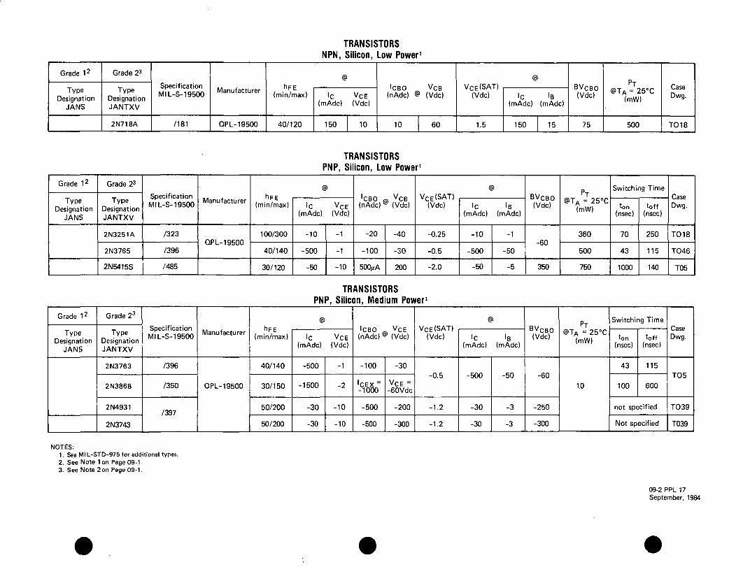
TRANSISTORSNPN, Silicon, Low Power1
Grade 12
TypeDesignation
JANS
Grade 23
TypeDesignationJANTXV
2N718A
SpecificationMIL-S- 19500
7181
Manufacturer
QPL- 19500
hFE(min/max)
40/120
@
ic(mAdc)
150
VCE(Vdc)
10
ICBO(nAdc) <3
10
VCB> (Vdc)
60
VCE(SAT)(Vdc)
1.5
@
ic(mAdc)
150
IB(mAdc)
15
BVcBO(Vdc)
75
PT<S>TA - 9^°r
(mW)
500
CaseDwg.
TO18
TRANSISTORSPNP, Silicon, Low Power1
Grade 12
TypeDesignation
JANS
Grade 23
TypeDesignationJANTXV
2N3251A
2N3765
2N5415S
SpecificationMIL-S- 19500
/323
7396
/485
Manufacturer
QPL- 19500
hFE(min/max)
100/300
40/140
30/120
@
ic VCE(mAdc) (Vdc)
-10
-500
-50
-1
-1
-10
ICBO ,5, VCB(nAdc) ® (Vdc)
-20
-100
500^A
-40
-30
200
VCE (SAT)(Vdc)
-0.25
-0.5
-2.0
@
ic IB(mAdc) (mAdc)
-10
-500
-50
-1
-50
-5
BVcBO(Vdc)
-60
350
PT@TA = 25°C
(mW)
360
500
750
Switching Time
ton(nsec)
70
43
1000
toff(nsec)
250
115
140
CaseDwg.
T018
TO46
T05
TRANSISTORSPNP, Silicon, Medium Power1
Grade 12
TypeDesignation
JANS
Grade 23
TypeDesignationJANTXV
2N3763
2N3868
2N4931
2N3743
SpecificationMIL-S- 19500
/396
/350
/397
Manufacturer
QPL-19500
hFE(min/max)
40/140
30/150
50/200
50/200
@
ic VCE(mAdc) (Vdc)
-500
-1500
-30
-30
-1
-2
-10
-10
ICBO ^ VCE(nAdc) @ (Vdc)
-100
-CIEOXOO=
-500
-500
-30
VCE =-eovdc
-200
-300
VCE (SAT)(Vdc)
-0.5
-1.2
-1.2
@
ic IB(mAdc) (mAdc)
-500
-30
-30
-50
-3
-3
BVCBO(Vdc)
-60
-250
-300
PT@TA = 25°c
(mW)
1.0
Switching Time
ton(nsec)
43
100
toff(nsec)
115
600
not specified
Not specified
CaseDwg.
TO 5
T039
T039
NOTES:1. See Ml L-STD-975 for additional types.2. See Note 1 on Page 09-1.3. See Note 2 on Page 09-1.
09-2 PPL 17September, 1984

TRANSISTORSNPN, Silicon, Medium Power1
Grade 12
TypeDesignation
JANS
Grade 23
TypeDesignationJANTXV
2N1613
2N3019
2N5662
SpecificationMIL-S- 19500
/181
/391
/454
Manufacturer
QPL- 19500
hFE(min/max)
40/120
100/300
40/120
<a
lc VCE(mAdc) (Vdc)
150
150
500
10
10
5
'CBO _ VCB(nAdc)@(Vdc)
10
ICES =
10nAdc
100
60
VCE =90Vdc
200
VCE (SAT)(Vdc)
1.5
0.2
0.4
@
lc IB(mAdc) (mAdc)
150
150
1000
15
15
100
BVCBO
(Vdc)
75
140
250
PT@TA =25°C
(mW)
800
1200
Switching Time
ton(nsec)
toff(nsec)
not specified
250 850
CaseDwg.
T05
TRANSISTORSPNP, Chopper, Low Power, Silicon1
Grade 12
TypeDesignation
JANS
Grade 23
TypeDesignationJANTXV
2N2944A
2N2946A
MIL-S- 19500
/•3OO
Manufacture
DPI iQ^nn
her
(min)
100
50
@
lc(mAdc)
VCE(Vdc)
n c.
(max)(Ohms)
4
8
f = 1kHzi_ — nIE u
@> andIB U
(mAdc) (M A)
1 inn
(max)(Vdc)
-0.6
-2.0
<£
IE(mAdc)
o
IB(mAdc)
i
BVnorv
(Vdc)
-15
-40
p<t-"T@TA = 25°c
(mW)
4nn
CaseDwg.
TOdfi
NOTES:1. See MIL-STD-975 for additional types.2. See Note 2 on Page 09-1.3. See Note 3 on Page 09-1.
09-3 PPL 17September, 1984

TRANSISTORSNPN, Silicon, High Power1 3
Grade 12
TypeDesignation
JANS
Grade 23
TypeDesignationJANTXV
2N2880
2N5250
2N5660
2N6546
SpecificationMIL-S-19500
/315
7380
/454
/525
Manufacturer
QPL- 19500
hFE(min/max)
40/120
30/90
40/120
16/30
<°>
ic VCE(Adc) (Vdc)
1
20
0.5
10
5
5
5
2
ICBO a -VCB(mAdc) ® (Vdc)
0.0004
ICES =0.1 mAdc
0.0001
1
80
VCE =125 Vdc
200
600
VCE (SAT)(Vdc)
0.25
1.0
0.4
1.5
<5>
lc IB(Adc) (Adc)
1
40
1
10
0.1
4
0.1
2
BVcBO(Vdc)
110
125
250
300
@TC =T25°C(Watts)
30@TC=125°C
350
20@TC = 125°C
175
CaseDwg.
Note 4
Note 4
T066
T03
TRANSISTORSPNP, Silicon, High Power1
Grade 12
TypeDesignation
JANS
Grade 23
TypeDesignationJANTXV
2N3741
2N3792
2N5745
SpecificationMIL-S-19500
/441
/379
/433
Manufacturer
QPL- 19500
hFE(min/max)
30/100
50/150
15/60
@
ic VCE(Adc) (Vdc)
-0.250
-1
-10
-1
-2
-2
ICBO @ VCB(mAdc) L (Vdc)
-0.0001
ICES =-1mAdc
-1
-80
VCE =-70Vdc
-80
VCE(SAT)(Vdc)
-0.6
-1
-1
<a
ic IB(Adc) (Adc)
-1
-5
-10
-0.125
-0.5
-1
BVcBO(Vdc)
-80
• PT@TC = 25°C
(Watts)
25
150
200
Switching Time
ton(/u sec)
0.4
1.5
1.0
toff(AI sec)
1.0
2.0
3.0
CaseDwg.
T066
T03
NOTES:1. See MIL-STD-975 'or additional types.2. See Note i on Page 09-1.3. See Note 2 on Page 09-1.4. This case does not meet the dimensional criteria for any JEDEC outline. See MIL-S-19500 detail specification for case outline dimensions.
09-4 PPL 17September, 1984

TRANSISTORSField-Effect, N-Channel, Junction, Silicon^
Grade 12
TypeDesignation
JANS
Grade 23"
TypeDesignationJANTXV
2N3821
2N3822
2N4857
2N4858
SpecificationMIL-S-19500
/375
/385
Manufacturer
QPL-19500
VDG and VDS(max)(Vdc)
50
40
VGS(max)(Vdc)
-50
-40
IG(mA)
10
50
VGs(off)max.(Vdc)
-4
-6
-4
@
VDS ID(Vdc) (nA)
15 0.5
IDSS(min/max)
(mA)
0.5/2.5
2/10
20/100
8/80
@
VDS VGS(Vdc) (Vdc)
15 0
PT(mW)
300
360
CaseDwg.
T072
T018
NOTES:1. See MIL-STD-975 for additional types.2. See Note 1 on Page 09-1.3. See Note 2on Page 09-1.
09-5 PPL 17September, 1984

INDEX TO PREFERRED MICROCIRCUITSi 2,3.4DIGITAL
(Generic Part Numbers Shown)
Low Power Schottky.TTL
54LSOO 54LS51 54LS139 54LS241 54LS39554LS02 54LS54 54LS148 54LS244 54LS49054LS03 54LS73 54LS151 54LS245 54LS67054LS04 54LS74 54LS153 54LS25154LS05 54LS75 54LS156 54LS25354LS08 54LS76 54LS157 54LS25754LS10 54LS83A 54LS158 54LS25854LS11 54LS85 54LS160 54LS25954LS12 54LS86 54LS161 54LS26654LS13 54LS90 54LS162 54LS27354LS14 54LS92 54LS163 54LS279
.54LS15 54LS93 54LS164 54LS28354LS20 54LS95 54LS165 54LS290 '54LS21 54LS96 54LS166 54LS29354LS22 54LS107 54LS174 54LS29554LS26 54LS109 54LS175 54LS29854LS27 54LS112 54LS190 54LS34854LS28 54LS113 54LS191 54LS36554LS30 54LS114 54LS192 54LS36654LS32 54LS122 54LS193 54LS36754LS37 54LS123 54LS194 54LS36854LS38 54LS126 54LS195 54LS37554LS42 54LS132 54LS197 54LS39054LS47 54LS138 54LS240 54LS393
Advanced Low Power Schottky, TTL (Refer to page 10-4)
54ALSOO 54ALS08 54ALS20 54ALS13354ALS02 54ALS10 54ALS27 54ALS13854ALS04 54ALS11 54ALS30 54ALS200A
54ALS244A
5401 5423 5470 54121 541635406 5425 5472 54145 54180A ' "5407 5450 5477 541505416 5453 5482 54154
CMOS/Bulk
4000A 4019A 4069UB"4002A 4020A 4070B4006A 4021 A 4071 B4007A 4022A 4072B4008A 4023A 4073B4009A 4024A. 4075B" .4010A 4025A 4077B"4011 A 4027A 4081 BR
401 3A 4031 A 4082BR
401 4A 4043A 4085BR
401 5A 4049A 4086B"401 6A 4050A 4098B"4018A 4066A 4099BR
4502BR
(Refer to page 10-5)
4001 B 401 2BR 40308"."4017B" 4020B"
Memory
• Prom, Schottky TTL
82S126 82S131 82S18182S129 82S136 82S18582S130 82S137 82S191
82S2708
• Ram, Schottky TTLQQI /I09 Q*3I A99A Q*3I A'jf*yj \J\££. JoLH l̂H 3OL*i£D
...._„ 93L415• Ram, NMOSMK2164
Microprocessor, NMOS
8080A 8086 Z80A Z8002
Microprocessor, I2L
9989
Hybrid(Refer to page 10-3)
NOTES:1. All parts are listed in MIL-STD-975 except as referenced otherwise. The parts must be purchased to the part
numbers specified in MIL-M-38510.2. When no Grade 1 microcircuit is listed, a Grade 2 microcircuit may be upgraded for use in Grade 1 applications
in accordance with Appendix A. A non-standard part approval is required.3. Refer to Appendix D for information on radiation effects.4. The part types marked with superscripts R and H can be procured as radiation hard parts, hardened to 1 x 10⁵ rads
and 1 x 10⁶ rads, respectively.10-1 PPL 17September, 1984

INDEX TO PREFERRED MICROCIRCUITSi-2,3,4 (Continued)
LINEARBIPOLAR AND BI-FeT
Operational Amplifiers
HA2600 LM101AHA2101A LM108AHA2500 LM118HA2510 LM124HA2520 LM148LF155 LM741LF156 LM747ALF156A LM1558LF157A LH2101A
Line Drivers961455113
Voltage Regulators
LM109 LM120K-15LM723 LM140H-12LM120H-05 LM140H-15LM120H-12 LM140K-05LM120H-15 LM140K-12LM120K-05 LM140K-15LM120K-12
Line Receivers Precision Timers
9615 55555107 55655108
Voltage Comparators
LM111LM139LM710
DAC Switches08 155 A08A 200
201
10-2 PPL 17September, 1984

HYBRID MICROCIRCUITS
Hybrid microcircuits are defined as microcircuits in which the circuits elements are contained on more than onedie or chip, as compared to a monolithic microcircuit where all the circuit elements are contained on a singledie. A hybrid microcircuit generally contains an insulating substrate or substrates on which are deposited aconductor network and sometimes thick film resistors. Semiconductor dice and sometimes passive elementsare attached to the substrate. Additional connections are made between the active and passive elements, thesubstrate, and the package leads using interconnection wires. Hybrid microcircuits are normally low volumenon-standard parts. A non-standard part approval is required for all non-standard types. General requirementsfor hybrid microcircuits are presented in GSFC specification S-311-200.
10-3 PPL 17September, 1984

MICROCIRCUITSDigital, MIL-M-38510 Advanced Low Power Schottky TTL
CommercialPart Number'
54ALSOO
54ALS02
54ALS04
54ALS08
54ALS10
54ALS11
54ALS20
54ALS27
54ALS30
54ALS133
54ALS240A
54ALS244A
54ALS138
Function
Gates
Buffers
Decoders
NAND, quad 2-input
NOR, quad 2-input
Hex Inverter
And, quad 2-input
NAND, Triple 3-input
AND, Triple 3-input
NAND, dual 4-input
NOR, Triple 3-input
NAND, 8-input
NAND, 13-input
Octal, inverting buffer
Octal, noninverting buffer
Single 3 to 8 line decoder
Grade 1
Part No. Manu-JANM38510 facturer
Note 3
Grade 2
Part No.2
JANM38510
/37001BXX
/37301BXX
/37006BXX
/37401 BXX
/37002BXX
/37402BXX
/37003BXX
/373002BXX
/37004BXX
/37005BXX
/38301BXX
/38303BXX
/37701BXX
Manu-facturer
PerQPL-38510
NOTES:1. Use the JANM38510 part number for ordering, not the commercial part number.2. The "XX's" are for choice of case outline and lead finish respectively. Refer to QPL-38510 for specific choices
available.3. No Grade 1 version of this part is presently being supplied by any manufacturer. The Grade 2 part may be used
for Grade 1 applications by upgrading in accordance with Appendix A. A non-standard part approval is required.
10-4 PPL 17September, 1984
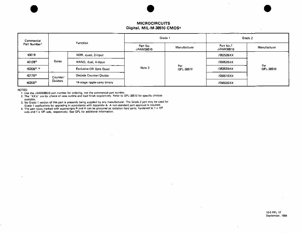
MICROCIRCUITSDigital, MIL-M-38510 CMOS'*
CommercialPart Number'
4001 B
4012B"
4030B". H
4017BR
4020B"
Function
Gates
Counter/Dividers
NOR, quad, 2-input
NAND, dual, 4-input
Exclusive-OR Gate Quad
Decade Counter/ Divider
14-stage ripple-carry binary
Grade 1
Part No.JANM38510
Note 3
Manufacturer
PerQPL-38510
Grade 2
Part No.2
JANM38510
/05252BXX
/05052BXX
/05353BXX
/05651BXX
/05653BXX
Manufacturer
PerQPL-38510
NOTES:1. Use the JANM38510 part number for ordering, not the commercial part number.2. The "XX's" are for choice of case outline and lead finish respectively. Refer to QPL-38510 for specific choices
available.3. No Grade 1 version of this part is presently being supplied by any manufacturer. The Grade 2 part may be used for
Grade 1 applications by upgrading in accordance with Appendix A. A non-standard part approval is required.4. The part types marked with superscripts R and H can be procured as radiation hard parts, hardened to 1 x 10⁵
rads and 1 x 10⁶ rads, respectively. See QPL for additional information.
10-5 PPL 17September, 1984

Index of Preferred Thermistors
Style
311P18
RTH
Description
Thermistor, Insulated, Negative Temp. Coeff.
Thermistor, Insulated, Positive Temp. Coeff.
Specification
GSFC S311-P-18
MIL-T-23648
Refer To
Page 14-2
MIL-STD-975
14-1 PPL 17September, 1984

THERMISTORS1
Temp.Coeff.
Neg.
Resistance(ohms)
2252
2252
3000
3000
5000
5000
10000
10000
30000
30000
Toleranceat 25°C
(±%)
1
0.5
1
0.5
1
0.5
1
0.5
1
0.5
OperatingTemperature
Range<°C)
-55 to 90
-55 to 70
-55 to 90
-55 to 70
-55 to 90
-55 to 70
-55 to 90
-55 to 70
-55 to 90
-55 to 70
ResistanceRatio
R25°C/RMAX
10.93
5.71
10.91
5.71
10.91
5.71
9.23
5.03
10.72
5.60
Grade 1 and Grade 2
Part Number2
311P18-01LXXX
311P18-02LXXX
311P18-03LXXX
311P18-04LXXX
311P18-05LXXX
311P18-06LXXX
311P18-07LXXX
311P18-08LXXX
311P18-09LXXX
311P18-10LXXX
Specification
GSFCS-311-P-18
Manufacturer
YellowSprings
Instrument
NOTES:1. WARNING: Use heat sinks when soldering or welding to thermistor leads.2. The complete part number is 311P18- AA L XXX
DASH NUMBER LEAD STYLE:(01,02, etc.) S= 32 AWG, Type C per MIL-STD-1276
T= 28 AWG, Type ET per MIL-W-1687-16878N= 32 AWG, Type N-2 per MIL-STD-1276E = Insulated lead (TFE), 32 AWG per
MIL-1-22129; Bare lead, Style S; Tubing(FEP),M23053/11-105c.
LEAD LENGTH:Specify length in centimeters.1RO = 1.0, 10R = 10, 101 = 100.Minimum length is 7.6cm.
14-2 PPL 17September, 1984

Index of Preferred Transformers
Style1
M27/103
M27/165
M27/166
M27/197
M21 038/9-005
Description
Audio Frequency
Audio Frequency
Audio Frequency
Audio Frequency
Pulse, Low Power
Specification
MIL-T-27
MIL-T-27
MIL-T-27
MIL-T-27
MIL-T-21038
Refer To
MIL-STD-975
MIL-STD-975
MIL-STD-975
MIL-STD-975
MIL-STD-975
NOTES:1. The purchase order must specify that 100% screening is required. Otherwise, when unscreened parts are purchased,
they shall be subjected to screening tests, as outlined in Table 15 of Appendix C prior to use.
15-1 PPL 17September, 1984

Index of Preferred Wire/Cable^
Style
M22759/9
M22759/18
M22759/32/33/34/35
S311P13
M22759/3/11/12/22/23
M22759/16
M81381
M 16878
M5086
M17
M27500-
Description
Wire, High temperature
Wire, Light weight, ETFE
Wire, Lightweight, crosslinked ETFE
Wire, High voltage
Wire, Extruded TFE
Wire, ETFE
Wire, Fluorocarbon-Polyimide
Wire, High Temperature
Wire, PVC insulated
Cable, RF, Flexible, Coaxial
Cable, Electrical, Shielded and Unshielded
Specification
MIL-W-22759
MIL-W-22759
MIL-W-22759
GSFC S-311-P-13
MIL-W-22759
MIL-W-22759
MIL-W-81381
MIL-W-16878
MIL-W-5086
MIL-C-17
MIL-C-27500
Refer To
Page 16-2
Page 16-3
Pages 16-3, 4, 5
Page 16-
MIL-STD-975
MIL-STD-975
MIL-STD-975
MIL-STD-975
MIL-STD-975
MIL-STD-975
MIL-STD-975
NOTES:1. GSFC WAIVES THE RESTRICTIONS AND REQUIREMENTS OF MIL-STD-975 ON THE USE OF SILVER
COATED COPPER CONDUCTOR WIRE AND CABLE.2. Flammability properties of these wires are controlled by the applicable specifications. However, applications in
Space Transportation System (STS) payloads may require that the specific STS flammability hazards be addressed.Users are advised to consult the appropriate project systems safety officer.
16-1 PPL 17September, 1984

WIREElectrical, Insulated, High Temperature
Style1
M22759/9-22-X
M22759/9-20-X
M22759/9-18-X
M22759/9-16-X
StrandsNo. x AWG #
1 9 x 3 4
1 9 x 3 2
1 9 x 3 0
1 9 x 2 9
Diameter overInsulation, mm
Minimum
1.47
1.68
1.93
2.11
Maximum
1.57
1.78
2.03
2.21
Voltage Rating,Maximum
(volts/RMS)
1000
SpecificationMIL-W-22759
/9
Grade 1 Grade 2
Manufacturer
QPL-22759/9
Remarks
NOTES:1. For the "X" suffix, substitute the appropriate color code designator from MIL-STD-681 (listed on page 16-7).
PPL 17fctember, 1984

WIREElectrical, Insulated, Lightweight (Page 1 of 3)
Style'
M22759/18-26-X
M22759/18-24-X
M22759/18-22-X
M22759/18-20-X
M22759/18-18-X
M22759/18-16-X
M22759/18-14-X
M22759/18-12-X
M22759/18-10-X
StrandsNo. x AWG #
19x38
19 x 36
19 x 34
19 x 32
19 x 30
19x29
1 9 x 2 7
37x28
37x26
Diameter overInsulation, mm
Minimum
.762
.864
1.04
1.24
1.50
1.65
2.01
2.57
3.15
Maximum
.864
.965
1.14
1.35
1.60
1.75
2.11
2.67
3.25
Voltage Rating,Maximum
(volts/RMS)
600
SpecificationMIL-W-22759
/1 8
Grade 1 Grade 2
Manufacturer
QPL-22759/18
Remarks
Tin-coatedcopper conductor
Insulated withextruded ETFE
Maximum tem-perature 1 50°C;suitable for useas hookup wire. .
NOTES:1. For the "X" suffix, substitute the appropriate color code designator from MIL-STD-681 (listed on Page 16-7).
16-3 PPL 17September, 1984

WIREElectrical, Insulated, Lightweight (Page 2 of 3)
Style1
M22759/32-30-XM22759/32-28-XM22759/32-26-XM22759/32-24-XM22759/32-22-XM22759/32-20-XM22759/32-18-XM22759/32-16-XM22759/32-14-XM22759/32-12-X
M22759/33-30-XM22759/33-28-XM22759/33-26-XM22759/33-24-XM22759/33-22-XM22759/33-20-X
StrandsMn v AWfi*IMU. A AAVVVJfr
7 x 3 87 x 3 6
19x3819 x3619 x3419x3219x3019x2919x2737 x28
7x387 x 3 6
19x3819x3619x3419x32
Diameter overInsulation, MM
Minimum
.559
.635
.762
.8891.041.221.471.682.082.54
.559
.635
.762
.8891.041.22
Maximum
.660
.737
.864
.9911.141.371.631.832.292.74
.660
.737
.864
.9911.141.37
Voltage Rating,Maximum
(volts, RMS)
600
600
Specification|\/1 1 1 \ A/ O9~7CQiviiL-vv-zz/Dy
/32
/33
Grade 1 Grade 2
Manufacturer
QPL-22759
QPL-22759
Remarks
Tin-coatedcopper conductor,insulated withcrosslined ETFE
Maximum temperature150°C
Silver coatedhigh strength copperalloy, Insulated withcrosslinked ETFE
Maximum temperature150°C
NOTES:1. For the "X" suffix, substitute the appropriate color code designator from MIL-STD-681 (Listed on Page 16-7).
16-4 PPL 17September, 1984

WIREElectrical, Insulated, Lightweight (Page 3 of 3)
Style'
M22759/34-24-XM22759/34-22-XM22759/34-20-XM22759/34-18-XM22759/34-16-XM22759/34-14-XM22759/34-12-XM22759/34-10-XM22759/34-8-XM22759/34-6-XM22759/34-4-XM22759/34-2-XM22759/34-1-XM22759/34-0-XM22759/34-00-X
M22759/35-26-XM22759/35-24-XM22759/35-22-X .M22759/35-20-X
StrandsMn v A\A/rc#tMU. A /AVVOrr
19x3619 x3419x3219x3019x2919x2737 x2837x26133x29133x27133 x 25665 x 30817 x 301045 x 301330 x 36
19 x3819x3619x3419x32
Diameter overInsulation, mm
Minimum
1.091.121.421.701.882.312.743.304.755.877.629.88
10.9011.9113.39
.9651.091.221.42
Maximum
1.191.371.571.852.082.512.953.615.166.388.13
10.7011.7112.7314.30
1.071.191.371.52
Voltage RatingsMaximum
(Volts/RMS)
600
600
Specification• yi|| %»/ OOTCQMIL-W-Zii/ba
/34
/35
Grade 1 Grade 2
Manufacturer
QPL-22759
QPL-22759
Remarks
Tin-coatedcopper conductorInsulated withcrosslinked ETFE.
Maximum temperature150°C
Silver-coated HighStrength Copper AlloyInsulated withcrosslinked ETFE.
Maximum temperature,200 °C.
NOTES:1. For the "X" suffix, substitute the appropriate color code designator from MIL-STD-681 (listed on page 16-7)
except that for sizes 2 and larger the braid color shall be dark green and the designator shall be 5D.
16-5 PPL 17September, 1984
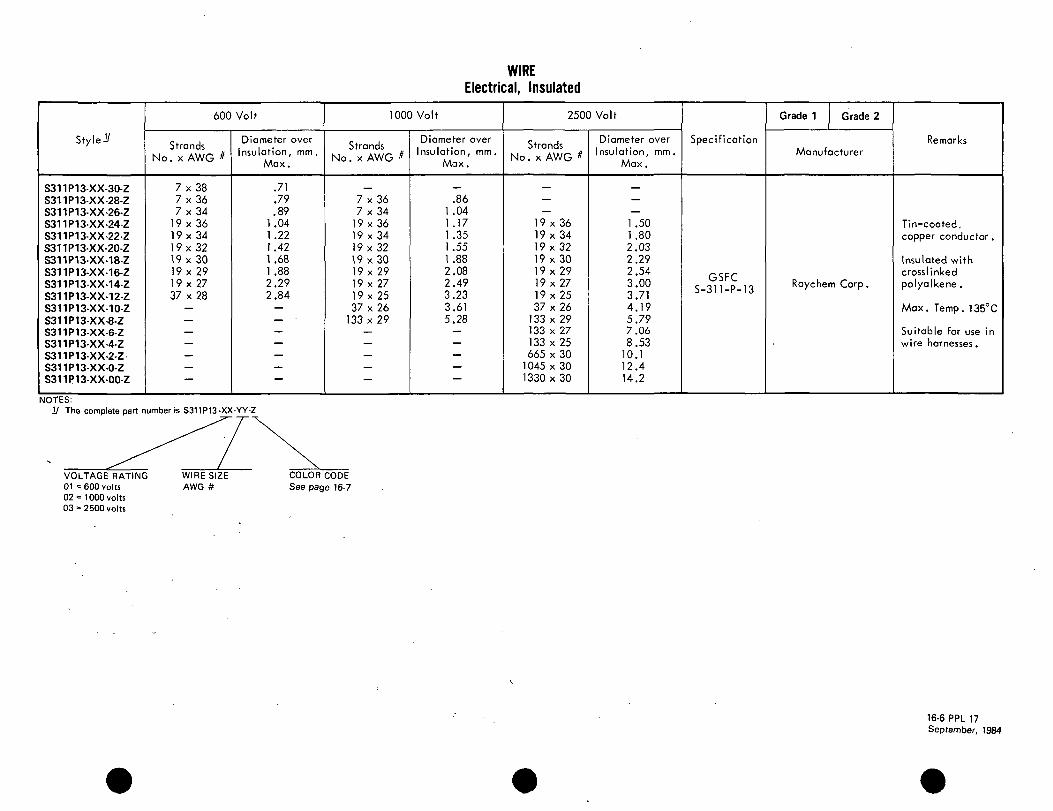
WIREElectrical, Insulated
Stylet
S311P13-XX-30-ZS311P13-XX-28-ZS311P13-XX-26-ZS311P13-XX-24-ZS311P13-XX-22-ZS311P13-XX-20-ZS311P13-XX-18-ZS311P13-XX-16-ZS311P13-XX-14-ZS311P13-XX-12-ZS311P13-XX-10-ZS311P13-XX-8-ZS311P13-XX-6-ZS311P13-XX-4-ZS311P13-XX-2-ZS311P13-XX-0-ZS311P13-XX-00-Z
600 Volt
StrandsNo . x AWG *
7 x387 x 3 67 x34
1 9 x 3 61 9 x 3 41 9 x 3 21 9 x 3 01 9 x 2 919 x 273 7 x 2 8
——_————
Diameter overInsulation, mm .
Max.
.71
.79
.891.041.221.421.681 .882.292.84
—— •————^
1000 Volt
StrandsNo . x AWG #
_,_
7 x367 x 3 4
1 9 x 3 61 9 x 3 419x3219x301 9 x 2 91 9 x 2 71 9 x 2 537 x 26
133 x 29__———
Diameter overInsulation, mm.
Max.
.861.041 .171.351.551 .882.082.493.233.615.28
—————
2500 Volt
StrandsNo . x AWG #
——
1 9 x 3 61 9 x 3 419x3219 x301 9 x 2 919 x 271 9 x 2 53 7 x 2 6
133 x 29133 x27133 x 25665 x 30
1045 x301330x30
Diameter overInsulation, mm .
Max .
——1.501.802.032.292.543.003.714.195.797.068.53
10.112.414.2
Specification
c;<;Fr\J jr v*.
S-311-P-13
Grade 1 Grade 2
Manufacturer
Raychem Corp.
Remarks
Tin-coated,copper conductor .
Insulated withcrosslinkedpolyalkene .
Max. Temp. 135°C
Suitable for use inwire harnesses .
NOTES:l/ The.complete part number is S311P13-XX-YY-Z
VOLTAGE RATING01 =600 volts02 = 1000 volts03 = 2500 volts
WIRE SIZEAWG#
COLOR CODESee page 16-7
16-6 PPL 17September, 1984

Color Code Designatorsfor Wire According to MIL-STD-681
BaseColor
BlockBrownRedOrangeYellowGreenBlueVioletGrayWhite
WhiteWhiteWhiteWhiteWhiteWhiteWhiteWhiteWhite
1stStripe
BlackBrownRedOrangeYellowGreenBlueVioletGray
2ndStripe
Designator
0123456789
909192939495969798
BaseColor
WhiteWhiteWhiteWhiteWhiteWhiteWhiteWhite
WhiteWhiteWhiteWhiteWhiteWhiteWhite
WhiteWhiteWhiteWhiteWhiteWhite
1stStripe
BlackBlackBlackBlackBlackBlackBlackBlack
BrownBrownBrownBrownBrownBrownBrown
RedRedRedRedRedRed
2ndStripe
BrownRedOrangeYellowGreenBlueVioletGray
RedOrangeYellowGreenBlueVioletGray
OrangeYellowGreenBlueVioletGray
Designator
901902903904905906907908
912913914915916917918
923924925926927928
BaseColor
WhiteWhiteWhiteWhiteWhite
WhiteWhiteWhiteWhite
WhiteWhiteWhite
WhiteWhite
1stStripe
OrangeOrangeOrangeOrangeOrange
YellowYellowYellowYellow
GreenGreenGreen
BlueBlue
2ndStripe
YellowGreenBlueVioletGray
GreenBlueVioletGray
BlueVioletGray
VioletGray
Designator
934935936937938
945946947948
956957958
967968
16-7 PL 17September, 1984

APPENDIX AUpgrading Grade 2 Devices
for Use in Grade 1 Applications
Both PPL-17 and MIL-STD-975 have sections in which no Grade 1 part is listed. This Ap-pendix lists what is recommended by GSFC to upgrade a Grade 2 part for use in a Grade 1 ap-plication. In most cases, GSFC guidelines are the same as those in MIL-STD-975. Where dif-ferences exist, they are defined in the appropriate paragraphs. In addition, the PPL providesupgrading alternatives to those described in MIL-STD-975 for semiconductor devices. Upgradedparts should be identified by a special marking on each piece or on the package. Where packagemarking is used, parts control procedures must be instituted so that the identity of upgraded partsis not lost. In all cases, the upgrading of a Grade 2 part for use in a Grade 1 application requiresa non-standard part approval request.
For the upgrading of diodes, transistors, microcircuits and filters, GSFC requires the sam-pling plan for destructive physical analysis (DPA) to be based on a "lot". A lot is defined as allparts with identical part numbers and lot-date codes.
The sampling plan for DPA, used in this Appendix, is taken from GSFC S-311-70. The sam-ple sizes shown below apply to all methods of upgrading of semiconductor devices given in thisAppendix.
Lot Size No. Samples<T~ I
5-15 216-50 3>50 5
A-1 PPL 17September, 1984

UPGRADING GUIDELINES
Section 1 — CAPACITORS
For styles listed in MIL-STD-975, see Appendix B of that document. For styles listed inPPL-17, where the appropriate Failure Rate is not available, a non-standard part approval is re-quired to use a part with the next higher failure rate.
Section 3 — FILTERS
Grade 2 filters listed in PPL-17 and MIL-STD-975 may be upgraded for use in Grade 1 ap-plications by performing the following additional sequence of tests and examinations:
(a) Visually examine the filters externally, for any damage or evidence of poor workmanshipin accordance with 4.6.1.1 of MIL-F-28861.
(b) Radiographic examination in accordance with 4.6.8 of MIL-F-28861.
(c) Thermal shock test in accordance with 4.6.2.1 of MIL-F-28861. The filters shall bemounted in accordance with 4.6.2.1b, therein. Following the test and measurements, thefilters shall be maintained in their torqued and mounted configuration for the subsequentvoltage conditioning tests.
(d) Voltage condition the filters for 168 hours in accordance with 4.6.2.2.2 of MIL-F-28861.In addition to the electrical measurements required after the conditioning, visually ex-amine the filters for any damage or evidence of physical degradation.
(e) Hermeticity tests on hermetically sealed filters in accordance with 4.6.9b of MIL-F-28861.The fine leak rate shall not exceed 1 x 10~7 atm cc/sec, and there shall be no continuousstream of bubbles emanating from the filter during gross leak tests.
(f) Destructive physical analysis in accordance with Appendix D of MIL-F-28861, except thatthe sample size shall be as shown on page A-l of this Appendix.
Section 4 — FUSES
GSFC considers the fuses in Section 4 of PPL-17 to be suitable for Grade 1 use when theyare screened according to Table 04 in Appendix C.
A-2 PPL 17September, 1984
Section 5 — INDUCTORS
For styles listed in MIL-STD-975, see Appendix B of that document.
Section 6 — RELAYS
If it is not possible to use one of the S-311-P-2(06) relays listed in PPL-17, then consult theparts specialist for advice in selection of a suitable relay.
Section 7 — RESISTORS
(a) When the appropriate Failure Rate is not available, a non-standard part approval is re-quired to use the next higher available rate.
(b) For resistor networks listed in MIL-STD-975, see Appendix B of that document, exceptthat a DPA shall be performed on a sample prior to the upgrading tests. See page A-l ofthis Appendix for the DPA sample size.
Section 8 — DIODES
Grade 2 JANTXV diodes listed in PPL-17 and MIL-STD-975 may be upgraded for use inGrade 1 applications by two methods:
(a) In accordance with Appendix B of MIL-STD-975.
(b) When a procurement consists of not more than 200 parts, perform destructive physicalanalysis on samples in accordance with GSFC S-311-70. Rescreen the JTXV diodes to theJANS screening requirements (except for internal visual inspection and stability tests).Power burn-in test on all parts in the lot should be extended to 360 hours with a P.O.A.of 10 percent. Measurements of electrical parameters for which delta limits are prescribedshall be made before and after the burn-in. All other electrical measurements should bemade only at the completion of the burn-in with limits as specified in the detail specifica-tion.
Referring to note 1, MIL-STD-975, Page B.4, diodes can be upgraded for Grade 1 use
without first rescreening them to Grade 2 level. If they have been subjected to screening verifica-tion tests (Appendix E), then tests already completed do not have to be repeated in upgrading theparts to Grade 1.
A-3 PPL 17September, 1984
Section 9 — TRANSISTORS
Grade 2 JANTXV transistors listed in PPL-17 and MIL-STD-975 may be upgraded for use inGrade 1 applications by two methods:
(a) In accordance with Appendix B of MIL-STD-975.
(b) When a procurement consists of not more than 200 parts, perform destructive physicalanalysis on samples in accordance with GSFC S-311-70. Rescreen the JTXV transistors tothe JANS screening requirements (except for internal visual inspection and stability tests).Power burn-in test on all parts in the lot should be extended to 360 hours with a P.O.A.of 10 percent. Measurements of electrical parameters for which delta limits are prescribedshall be made before and after the burn-in. All other electrical measurements should bemade only at the completion of the burn-in with limits as specified in the detail specifica-tion.
Referring to note 1, MIL-STD-975, Page B.4, transistors can be upgraded for Grade 1 usewithout first rescreening them to Grade 2 level. If they have been subjected to screening verifica-tion tests (Appendix E), then tests already completed do not have to be repeated in upgrading theparts to Grade 1.
Section 10 — MICROCIRCUITS
Grade 2 microcircuits may be upgraded for use in Grade 1 applications by two methods:
(a) In accordance with Appendix B of MIL-STD-975.
(b) When a procurement consists of not more than 200 parts, the upgrading requirementsgiven in Table 3.2 of Appendix B of MIL-STD-975 shall be used except that the DPA, :therein, shall be replaced with a DPA in accordance with GSFC S-311-70 and the GroupB tests of Appendix B eliminated.
Section 14 — THERMISTORS
For styles listed in MIL-STD-975, consult the parts specialist.
Section 15 — TRANSFORMERS
For styles listed in MIL-STD-975, see Appendix B of that document.
Section 16 — WIRE and CABLE
For styles listed in MIL-STD-975, consult the parts specialist.
MISCELLANEOUS
For device types listed in MIL-STD-975 but not in PPL-17, consult the parts specialist.
A-4 PPL 17September 1984

APPENDIX BParts Derating Factors
This Appendix tabulates GSFC's guidelines for the derating of the parts and device typeslisted in MIL-STD-975 and PPL-17. Many of these derating guidelines are identical to those givenin MIL-STD-975. However, where differences occur, the GSFC derating factors shall haveprecedence. If a derating factor is not provided here for a specific part type, consult the PartsSpecialist.
B-1 PPL 17September, 1984

Table 01.Derating Outline for Capacitors
Dielectric Class
Ceramic (CKR), (CDR), (CCR)
Plastic Film (CRH) (Note 1)
Glass or Porcelain (CYR)
Tantalum (Solid Electrolyte) (CSR)
> 1 ohm/volt effective circuitimpedance (Note 2)
Tantalum (Wet Electrolyte) (CLR)
Tantalum Foil (CLR)
Maximum AmbientOperating
Temperature °C
85
70
70
Derate to Following Percentage (%)
Rated Voltage
60
60
50
60
60
50
Ripple Voltage
N/A
75
NOTES:1. CRH styles are not approved for use in circuits where the energy is less than 250 jj joultes.
2. For applications where the effective circuit resistance is less than one ohm per volt, contact the PartsSpecialist.
B-2 PPL 17September, 1984

Table 02. Derating Outline for Connectors
Number of ContactsUsed in Connector
1 to 4
1 to 4
1 to 4
5 to 14
5 to 14
5 to 14
15 or more
15 or more
15 or more
Contact Size
16
20
22
16
20
22
16
20
22
Maximum Current Per Contact1 (Amperes)
Wire Size (AWG)
16
13.0
9.0
6.5
18
9.2
7.0
5.0
20
6.5
6.0
5.0
5.0
3.7
3.7
22
4.5
4.5
3.5
3.5
2.5
2.5
24
3.3
3.3
2.7
2.7
2.0
2.0
26
2.5
1.9
1.4
28
1.8
1.4
1.0
Maximum Operating Voltage
25% of rated DielectricWithstanding Voltage
NOTE:1. Maximum current may be carried by only 10% of the contacts at one time. At such time, other contacts should be limited to 100mA.
Table 03. Derating Outline for EMI Filters
Class
All Filters
Derate To
50% rated feed through current and50% rated DC working voltage
Maximum Ambient Temperature
85° C
B-3 PPL 17September, 1984

Table 04. Derating Outline for Fuses
Subminiature1'2-3'4
Fuse Current Rating(Amperes)
15, 10,7, 54,3 ,214,2
r/2, 1%
1/23/81/41/8
Derate to the Following(%) of Rated Current
50%45%40%
40%35%30%25%
Remarks
THE FLIGHT USE OF FUSES RATED V4 AMPERE ANDLESS REQUIRES APPLICATION APPROVAL BY THEAPPLICABLE GSFC PROJECT OFFICE.
NOTES:1. Derating factors are based on data from fuses mounted on printed circuit boards and conformally coated. For other type mount-
ings, consult the parts specialist for recommendations.2. Derating of fuses also allows for possible loss of internal gases in a space environment, which lowers the blow current
rating and allows for a decrease of current capability with time.3. Fuse current ratings are based on a measured blow current of 200% rated current for a maximum of 5 seconds to blow the fuse and
a minimum ratio of 4/1 of blow to operating current. The minimum of 4/1 of blow to operating currents corresponds to the 50%derating factor. An 8/1 ratio of blow to operating currents corresponds to the 25% derating factor for the 1/8 ampere fuse. Formaximum life in critical space applications, GSFC recommends an 8/1 ratio.
B-4 PPL 17September, 1984

Table 05.Derating Outline for Inductors/Coils1
ClassPer MIL-C-39010
-
A
B
• ClassPer MIL-C- 15305
O
A
B
Maximum OperatingTemperature
65° C
85° C
105°C
Derate To
50% of Maximum rated voltage .
NOTES:1. a) Maximum operating temperature equals ambient temperature + temperature rise 4- 10°C (allowance for hot spot).
Compute temperature rise as follows:Temperature rise (°C) = — (T + 234.5) - (T-t)
b)
Where R = Winding resistance under loadr = No load winding resistance at ambient temperature T(°C).
The insulation classes of MIL style inductive parts have maximum operating temperature ratings which are generally based upona life expectancy of at least 10,000 hrs. The maximum operating temperatures in this table are selected to extend the lifeexpectancy to 50,000 hrs.Custom made inductive devices shall be evaluated on a materials basis and stressed at levels below the maximum rated operatingtemperature for the materials used. Devices having a maximum rated operating temperature in the range of 85° C to 130°C, shallbe derated to: Maximum Operating Temperature (°C) = .75 x Maximum Rated Operating Temperature (°C). For devices withmaximum rated temperatures outside this temperature interval consult the parts specialist for temperature derating recom-mendations.
B-5 PPL 17September, 1984

Table 06.Derating Outline for Relays1
Class
All Relays
Derate To
50% of rated contact current
Remarks
Users are cautioned not to derate coil current or voltage,can result in non-operation of the device.
as this
NOTES:1. For additional derating guidelines, see MIL-STD-975, Appendix A.
Table 07.Derating Outline for Resistors
Type
Carbon composition, Style RCR
Film, General Purpose, Style RLR
Wirewound, Accurate, Style RBR
1 % Tolerance0.5% Tolerance0.1% Tolerance, or less
Wirewound, Power, .Chassis Mount, Style RER
Wirewound, Power, Style RWR
Variable Trimmers, Styles RTR & RJR
Film, High Stability, Style RNC
Film, Fixed, Networks, Style R20
Derate To
60% of Rated Power
60% of Rated Power
60% of Rated Power35% of Rated Power25% of Rated Power
60% of Rated Power
60% of Rated Power
70% of Rated Current
60% of Rated Power
60% of Rated Power
Remarks
All resistors:
(a) Maximum voltage shall not exceed 80% of themaximum rated voltage on any resistor.
(b) Resistors with weldable nickel leads shall bederated by an additional factor of 0.5
B-6 PPL 16September, 1984
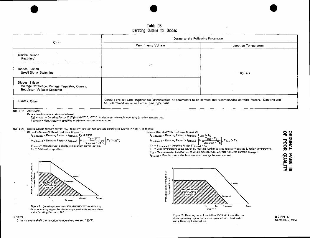
Table 08.Derating Outline for Diodes
Class
Diodes, SiliconRectifiers'
Diodes, SiliconSmall Signal Switching
Diodes, SiliconVoltage Reference, Voltage Regulator, CurrentRegulator, Variable Capacitor
Diodes, Other
Derate to the Following Percentage
Peak Inverse Voltage
75
Junction Temperature
60'. 2. 3
Consult project parts engineer for identification of parameters to be derated and recommended derating factors. Derating willbe determined on an individual part type basis.
NOTE 1: All DevicesDerate junction temperature as follows:
Tj(derated) = Derating Factor X (Tj(max)-25°C]+25°C. = Maximum allowable operating junction temperature.Tj(max) = Manufacturer's specified maximum junction temperature.
NOTE 2: Derate average forward current (lo) to satisfy junction temperature derating calculated in note 1, as follows:Devices Operated Without Heat Sink (Figure 1 )
loiallowed) ° Derating Factor X lo(max). TA < 25°C
lo(allowed) = Derating Factor X lo(max) l-= -I Tjtde
'o(max) = Manufacturer's absolute maximum current rating.TA • Ambient temperature.
- - zrs^ ,erated) - 25 CJ
TA > 25°C
Figure 1. Derating curve from MIL-HDBK-217 modified toshow operating region for devices operated without heat sinksand a Derating Factor of 0.6.
NOTES:3. In no event shall the junction temperature exceed 125°C.
Devices Operated With Heat Sink (Figure 2)loiallowedl = Derating Factor X lo(max|. Tease < TD
o o•n a
loisllowed) = Derating Factor X lo(max) I-Tcase ' TD 1
Tjlderated) - TDJ-TCase>TD
TD = Tj(deratedl - Derating Factor (Tj(rnax> - TM)TO = Case temperature above which IQ must be further derated to satisfy derated junction temperature.TM = Maximum case temperature at which manufacturer permits full rated current, (lomax).'loimax) = Manufacturer's absolute maximum average forward current.
TCASE —"
Figure 2. Derating curve from MIL-HDBK-217 modified toshow operating region for devices operated with heat sinksand a Derating Factor of 0.6.
B-7 PPL 17September, 1984

Table 09.Derating Outline for Transistors
Class
Silicon NPN, PNPLow power, Med. power, High power, Switching,Dual, Complimentary, Chopper, Unijunction.
J-FET, MOSFET, N-Channel, P-Channel, SiliconGeneral Purpose, Med. Power, High Power,High Speed Switching
RFNPN,Other
Derate to the Following Percentage
Voltage
75
Current
75
Power
60
Junction Temperature
60'. 2. 3
Consult project parts engineer for identification of parameters to be derated and recommended derating factors. Derating willbe determined on an individual part type basis.
NOTE 1: All devices:Derate junction temperature as follows:
Tj(derated) = Derating Factor X [Tj(max)-25°C]+25°C = Maximum recommended operating junction temperature.Tjmax = Manufacturer's specified maximum junction temperature.
NOTE 2: Derate power dissipation to satisfy the junction temperature derating calculated in Note 1,Devices operated without heat sink (Figure 1 )
PD (allowed) = Derating Factor X PD (max), TA < 25°C
.R0J-A
Pnmax = Mfr's absolute maximum power rating.R0j_A - Junction to ambient thermal resistance from mfr's data sheet ( C/watt).TA = Ambient temperature.
Slope =R0JA
Figure 1. Derating curve from MIL-HDBK-217 modified toshow operating region for devices operated without heat sinksand a Derating Factor of 0.6.
NOTE 3: In no event shall the junction temperature exceed 125°C.
as follows:Devices operated with heat sink (Figure 2)
PD (allowed) = Derating Factor X Pc(max), Tca.
PD(allowed) . ̂ (derated)-Tcase > '
R0jcTD = Tj(derated) - Rflj-c(Derating Factor X Pomax).TD = Case temperature above which power must be further reduced to satisfy junction temperature requirements.Pomax = Mfr's specified absolute maximum power rating.RfiJC = Junction to case thermal resistance specified in mfr's data sheet (°C/watt).
Slope •ROJC
Tjlderated} Tj(max)
Figure 2. Derating curve from MIL-HDBK-217 modified toshow operating region for devices operated with heat sinksand a Derating Factor of 0.6.
B-8 PPL 17September, 1984

Table 10Derating, Outline for Microcircuits1
MicrocircuitsParameters
1. Supply Voltages
2. Supply Current
3. Power Dissipation1
(percent of ratedpower at casetemperature)
4. Frequency(percent ofmaximum rating)
5. Output Current(percent ofrated current)
6. Input Voltage
Digital
BIPOLAR
±5% ofnominal
80%
90%
80%
CMOS4000
Series
90% ofrated
80%
90%
80%
Interface
A/DConverters
±5% ofnominal
80%
90%
D/AConverters
±5% ofnominal
80%
90%
LineReceivers
±5% ofnominal
80%
90%
80%
LineDrivers
+ 5% ofnominal
80%
90%
80%
AnalogSwitches
90% ofrated
80%
90%
Linear
Opera'l.Anpl.
80%of rated
75%
90%
80%
70%
VoltageCompara
tors
90% ofrated
75%
80%
VoltageReq.
75%
80%
90%
AnalogSwitches
90%of rated
75%
90%
80%
Processors, Peripheralsand Memories
CMOS
± 5% ofnominal
75%
90%
TTL
±5% ofnominal
75%
90%
NMOS
±5% ofnominal
75%
90%
|2L
± 3% ofnominal
75%
90%
NOTES:1. The maximum case temperature is 85°C for all microcircuits.
B-9 PPL 17September, 1984

Table 14.Derating Outline for Thermistors
(Temperature Sensitive Resistor]
Class
All Thermistors
Derate To
50% of rated power
Table 15.Derating Outline for Transformers
ClassPer MIL-T-27
Q
R
. .s
ClassPer MIL-T-21038
Q
R
S
Maximum OperatingTemperature^
65° C
85°C
105°C
Derate To
50% of Maximum rated voltage .
NOTES:1. a) Maximum operating temperature equals ambient temperature + temperature rise + 10°C (allowance for hot spot).
Compute temperature rise as follows: pTemperature rise (°C) = ̂ (T + 234.5) • (T -1)
Where R = Winding resistance under load.r = No load winding resistance at ambient temperature T(°C).t = Initial ambient temperature (°C).T = Ambient temperature at power shutoff. T shall not differ from t by more than 5°C.
b) The insulation classes of MIL style inductive parts have maximum operating temperature ratings which are generally based upona life expectancy of at least 10,000 hrs. The maximum operating temperatures in this table are selected to extend the lifeexpectancy to 50,000 hrs.
c) Custom made inductive devices shall be evaluated on a materials basis and stressed at levels below the maximum ratedoperating temperature for the materials used. Devices having a maximum rated operating temperature in the range of 85°Cto 130°C, shall be derated to: Maximum Operating Temperature (°C) = .75 x Maximum Rated Operating Temperature (°C).For devices with maximum rated temperatures outside this temperature interval consult the parts specialist for temperaturederating recommedations.
B-10 PPL 17September, 1984
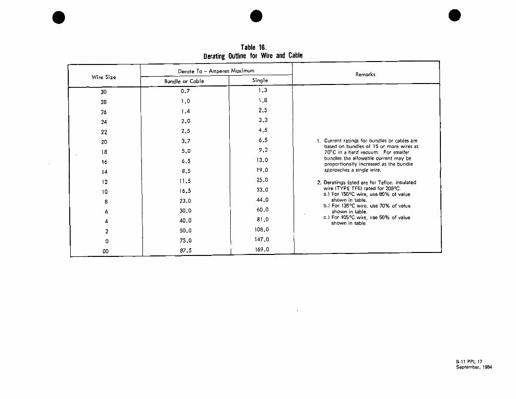
Table 16.Derating Outline for Wire and Cable
Wire Size
30
28
26
24
22
20
18
16
14
12
10
8
6
4
2
0
00
Derate To - Amperes Maximum
Bundle or Cable
0.7
1.0
1.4
2.0
2.5
3.7
5.0
6.5
8.5
11.5
16.5
23.0
30.0
40.0
50.0
75.0
87.5
Single
1.3
1.8
2.5
3.3
4.5
6.5
9.2
13.0
19.0
25.0
33.0
44.0
60.0
81.0
108.0
147.0
169.0
Remarks
1. Current ratings for bundles or cables arebased on bundles of 15 or more wires at70°C in a hard vacuum. For smallerbundles the allowable current may beproportionally increased as the bundleapproaches a single wire.
2. Deratings listed are for Teflon insulatedwire (TYPE TFE) rated for 200°C.a.) For 150°C wire, use 80% of value
shown in table.b.) For 135 °C wire, use 70% of value
shown in table.c.) For 105 °C wire, use 50% of value
shown in table.
B-11 PPL 17September, 1984

APPENDIX CScreening of Non-standard Parts
This PPL is intended to serve as a selection source for standard parts that are properly pro-cessed and screened for use in high-reliability space flight applications. Where non-standard partsare selected for use, proper processing and screening of those parts must be determined and ap-plied. Such determinations are the responsibility of the user, with parts engineering assistance, andmust consider the type of part, its function, its design, construction, and manufacturing, as well asits significant failure modes and sensitivities. Such a screening program must be developed with theknowledge of the part's response to use, and to qualification and evaluation testing exercises.
This appendix tabulates a series of recommended screening tests for various types of parts. Itis not the intent to delineate an exacting or all-inclusive set of detailed test procedures and re-quirements for each of a myriad of possible non-standard part selections. Rather, it is intended tostimulate the design of a detailed screening regimen to be incorporated in the part procurementdocument or screening specification. It brings to bear the combined experiences and knowledge ofGSFC and GSFC contractor parts engineers to act as a guide in developing screening for specificparts. It is not intended to be a "cookbook" to be applied without careful consideration of thepart to be screened. Furthermore, since there is generally a smaller data base for non-standardparts than preferred parts, the user must assure himself that the specified screens are non-destructive, appropriate parameters and limits are prescribed, and a lot "Percent DefectiveAllowable" (PDA) is included.
Other techniques, such as Destructive Physical Analysis (DPA), Residual Gas Analysis(RGA), Lot Acceptance Inspections, etc. should be applied where appropriate.
C-1 PPL 17September, 1984

Table 01.Screening Outline for Capacitors
^^^^ Test Sequence
Category • ^^^^
(a) Air or Glass, Variable
(b) Ceramic
(c) Glass & Porcelain
(d) Mica
(e) Paper and/orplastic film
(f) Polycarbonate,metallized film
(g) Tantalum Electrolytic,Wet Slug
Foil
(h) Tantalum Electrolytic,Solid
UiHermetically sealed
(2INon-hermetically sealed
(i) High Voltage Ceramic(Note 7)
12,3
Initial Examinationsand Electrical Tests
Visual &C, Q, DWV
IR, Driving Torque
Visual &C, DF, DWV, IR
Visual &C, DF
DC Leakage
Visual &C, DF, IR, DWV,
Corona
2
Thermal ShockMIL-STD-202,
Method 107
Test Condition A,except step 3
shall be @ max.rated temperature
Test Condition B,except step 1
shall be @ - 55°C
Test Condition A,except step 3
shall be @ max.rated temperature
Test Condition A,except step 3
shall be @ 100°C.
TestCondition
A
Test ConditionA
38
Seal Leak TestsMIL-STD-202,
Method 112
N/A
Test Condition D
Test ConditionsC, D
Acid Indicatortest per GSFC
SP 01 .23
Test ConditionsD
Test Condition D
N/A
N/A
4
RadiographicMIL-STD-202,
Method 209
N/A
In accordance withMIL-C-39014.N/A to chip
styles
N/A
In accordance withMIL-C-19978
N/A
In accordance withMIL-C-39003
N/A
5 .
Conditioning
N/A
2 x rated voltage @max. rated tempera-
ture for 96 hours(Note 4)
2 x rated voltage @125°C for 96 hours
2 x rated voltage @max. rated tempera-
ture for 96 hours
1.4 x rated voltage@rated temperature
for 96 hours
1 .4 x rated voltage @100°C for 96 hours
Rated voltage (3>85° C for 168 hours
Rated voltage. @ 85°C(Note 5)
Rated Voltage @ 85°Cand
Surge Current TestPer MIL-C-39003/6
(Note 6)
Rated Voltagerated Temperature
100 hours
69
Final Examination
RepeatInitial
Examinationand
ElectricalMeasurements
ReferenceDocuments
MIL-STD-202
Ml L-C- 14409
MIL-C-20MIL-C-39014MIL-C-55681
MIL-C-23269
MIL-C-39001
MIL-C-19978
MIL-C-83421
MIL-C-39006GSFC
SP 01 .23
MIL-C-39003
GSFCS-311-P-17(01)
GSFCS-311-P-15(01)
O Q
§g50 !-•
o 3c >>r~ rn
3a
(I/ i ny •
NOTES: i.2.3.4.5.6.7.8.
C-2 PPL 17September, 1984
Test procedures and requirements in accordance with those in the applicable Military or NASA referenced document. For additional information see the referenced document.Legend: C = Capacitance, DF = Dissipation Factor, DWV = Dielectric Withstanding Voltage, IR = Insulation Resistance, Q = Quality Factor (initial electrical tests are optional).Insulation resistance measurements are normally performed at +25°C, but the option is made to perform this measurement at maximum rated temperature as well.Voltage conditioning shall be performed using procedures and requirements of MIL-C-39014 Rev. C or later.Voltage conditioning shall be conducted for 168 hours for polarized styles. For non-polarized styles, voltage conditioning shall be conducted for 192 hours with the voltage polarity reversed after 96 hours.Surge current testing shall be performed on CSR style capacitors for all Grade 1 applications. Where the effective series resistance is < one ohm/volt, consult Part Specialist.Testing at high voltage (DWV, corona) shall be limited to the rated voltage.Seal leak tests apply only to hermetically sealed, unsleeved styles; however, the acid indicator test is requiredon all tantalum wet slug styles.Final IR measurements to be made at both +25°C and at max. rated temperature.

Table 03.Screening Outline for EMI Suppression Filters2
\ Test\Sequence
Category^V
Filters, EMISuppression(with CeramicCapacitorElements)
For Both
Grade 1/Grade 2 parts
1
Initial Measurementsand examination
1. Visual2. Dielectric Withstanding
Voltage (DWV)3. Capacitance (when
applicable)4. Dissipation Factor
(DF) (when applicable)5. Insulation Resistance
(IR) at + 25°Cand op-tional at max. ratedtemperature.
6. D.C. Resistance7. Radiographic examina-
tion, Grade 1 only.
2
Thermal Shock3'4
As per MIL-STD-202,Method 107 Test ConditionCondition A; exceptthat in step 3, sampleunits shall be tested at125°C, or max. ratedtemperature.
3
Seal Leak Test
Fine and Gross Leaktests (applicable tohermetically sealeddevices only).
4
Voltage
Conditioning^ 6
As per MIL-STD-202, Method108 at testtemperature+ 125°C, or max.rated temperature,±3°C. DC ratedfilter is 2X ratedvoltage for 164 ± 4hours. AC ratedfilter is 1 .2X ratedvoltage for 164 ± 4hours.
5
Final Measurementsand examination
Repeat initialexaminations andmeasurements.except radiographicexaminations. Finalmeasurements to bemade at both + 25°C'and at max. ratedtemperature.
ReferenceDocuments
MIL-F-28861
MIL-STD-202
NOTES:1. Performance of initial electrical tests is optional.2. Consult the parts specialist for assistance in screening other types of filters.3. Filters shall be mounted in a thru-hole and torqued in place on a rigid metal plate to the specified value. Not
applicable to solder-in types.4. At completion of or during the final cycle and before the filter is removed from the plate, measure and record
insulation resistance at + 125°C, or maximum rated temperature.5. For voltage conditioning, use the test circuit described in MIL-F-28861, par. 4.6.2.2.2d.6. After completion of voltage conditioning and while still at + 125°C, or maximum rated temperature, the insulation
resistance shall be measured per MIL-F-28861, par. 4.6.13.
C-3 PPL 17September, 1984
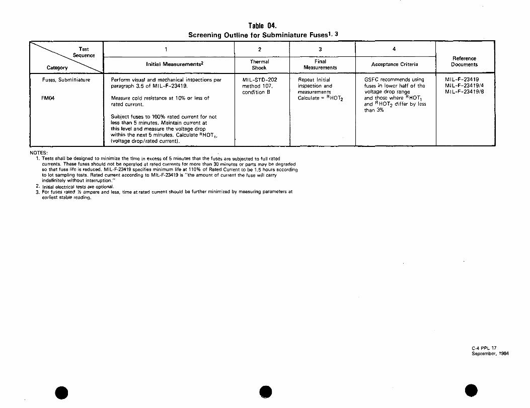
Table 04.Screening Outline for Subminiature Fuses'1- 3
^^-^^ Test^^ Sequence
Category ^^\^^
Fuses, Subminiature
FM04
1
Initial Measurements2
Perform visual and mechanical inspections perparagraph 3.5 of MIL-F-23419.
Measure cold resistance at 10% or less ofrated current.
Subject fuses to 100% rated current for notless than 5 minutes. Maintain current atthis level and measure the voltage dropwithin the next 5 minutes. Calculate RHOT,,(voltage drop/rated current).
2
ThermalShock
MIL-STD-202method 107,condition B
3
FinalMeasurements
Repeat Initialinspection andmeasurementsCalculate = RHOT2
4
Acceptance Criteria
GSFC recommends usingfuses in lower half of thevoltage drop rangeand those where RHOT1
and RHOT2 differ by lessthan 3%
ReferenceDocuments
MIL-F-23419MIL-F-23419/4MIL-F-23419/8
NOTES:1. Tests shall be designed to minimize the time in excess of 5 minutes that the fuses are subjected to full rated
currents. These fuses should not be operated at rated currents for more than 30 minutes or parts may be degradedso that fuse life is reduced. MIL-F-23419 specifies minimum life at 110% of Rated Current to be 1.5 hours accordingto lot sampling tests. Rated current according to MIL-F-23419 is "the amount of current the fuse will carryindefinitely without interruption."
2- Initial electrical tests are optional.3. For fuses rated Vi ampere and less, time at rated current should be further minimized by measuring parameters at
earliest stable reading.
C-4 PPL 17September, 1984

Table 05.Screening Outline for Inductors/Coils
^\^ Test^^^Sequence
Category v^^
Coils, Fixed,Molded, RF
Coils, Audioand Power
1
Initial Measurements
1 . Visual Inspection2. D . C . Resistance3. Insulation Resistance (IR)4. Dielectric Withstanding Voltage (DWV)5. Inductance (L)6. Q7. Self Resonant Frequency (SRF)
1. Visual Inspection2. D.C. Resistance3. Insulation Resistance (IR)4. Dielectric Withstanding Voltage (DWV)5. Inductance (L)6. Q7. Self Resonant Frequency (SRF)
2
Thermal Shock
MIL-STD-202 Method107, Condition A-l ,use maximum operatingtemperature of coil .
MIL-STD-202 Method 107,Condition A-1, Usemaximum operatingtemperature of coil.
3
Burn-In
MIL-STD-981Par. 30.1.2.2
MIL-STD-981Par. 30.1.2.1.2
4
Final Measurementsand Delta
Reject Criteria
Visual InspectionRepeat initialmeasurements .
RejectAR>±5%AL>±5%
Visual Inspection.Repeat initialmeasurements.Reject:
AR>±5%AL> ±5%
ReferenceDocument
MIL-C-39010MIL-STD-981
MIL-T-27MIL-STD-981
C-5 PPL 17September, 1984

Table 06.General Screening Outline for Relays1 6
Test Sequence
Category
Relays - Latchingand Non-Latching
1
InitialVisual
Examination
a. ExternalVisual a
b. Pre-CapVisual
2
InitialSeal Leak
Tests
MIL-STD-202Method 112
Fine leaksTest Cond. C
Gross leakTest Cond. D
3
InitialElectrical
Measurements3
CoilResistance
Pull In andDrop OutVoltage5
ContactResistance
ContactTransfer
Characteristics
InsulationResistance
DielectricStrength
4
SinusodialVibration4
10-2000 Hz30 g peak
5
High TempSoak Test
8 hrs. soakat 125°C
6
Low TempMiss Test
1000operationmiss testat -65°C
7
Room TempMiss Test
5000operationmiss testat 25°C
8
FinalSeal Leak
Test
Repeat testsequence
no. 2
9
FinalElectrical
Measurements
Repeat testsequence
no . 3
10
FinalVisual
Examination
ExternalVisual
NOTES:1. These screening tests are to be performed per GSFC S-311-P2I06) in the sequence shown. When the screening is
performed by the relay manufacturer, the initial external visual (1), seal leak (2) and electrical measurements (3) areoptional. For additional information, consult the Parts Specialist.
2. Pre-cap visuals are applicable only to parts procured to specification, e.g. a source control drawing (SCO), whichincludes pre-cap visual accept/reject criteria.
3. The test sequence of electrical measurements is optional; also, the performance of initial electrical measurements is optional.4. For relays rated at higher than 30g, consult the Parts Specialist for screening g-level.5. Drop out voltage is not applicable to latching relays.6. A DESTRUCTIVE PHYSICAL ANALYSIS (DPA) SHALL BE PERFORMED PER GSFC-S-311-70 IF PRE CAP
VISUAL IS NOT PERFORMED.
C-6 PPL 17September, 1984

Table 07. (Page 1 of 2)Screening Outline for Resistors
^^-^^ Test^ •̂̂ ^^ Sequence
Category -^^^
Resistors, Fixed, CarbonComp.
Resistors, Fixed, Film,General Purpose
Resistors, Fixed, Film,High Stability
Resistors, Fixed, Wirewound,Power
Resistors, Fixed,Wirewound, Power,
Resistors, Fixed,Wirewound, Power, ChassisMount
1
InitialMeasurements
Visual InspectionResistance
Visual InspectionResistance
Visual InspectionResistance
Visual InspectionResistance
Visual InspectionResistance
Visual InspectionResistance
2
Thermal Shock
—
-
MIL-STD-202Method 107Cond . F
—
—
-
3
Conditioning
-
1 .5 x rated power at room temperaturefor 24 hours .
Mil. equivalent styles:Style 50, 55, 60: 5 x rated power at
room temperature for 1 hour.Style 65: 4 x rated power at room
temperature for 1 hour.Style 70 and 75: 2.25 x rated power
at room temperature for 1 hour.Style 90: 6.25 x rated power for 5
seconds at room temperature.
1 .0 x rated power for 1 .5 hours on,0.5 hour off for 100 hours at 25°C.
1 .0 x rated power for 1 .5 hours on,0.5 hour off for 100 hours at 25°C .
1 .0 x rated "free air" power for 1 .5hours on, 0.5 hour off for 96 hoursat 25° C .
4
Seal Leak Test1
—
-
MIL-STD-883Method 1014Cond. D(For hermeticallysealed units)
-
-
—
5
Final Measurements andDelta Reject Criteria
-
Visual InspectionResistanceReject; AR>±0.5%
Visual InspectionResistanceReject: AR>±0.2%Style 90: AR>±0.05%
Visual InspectionResistanceReject: AR>±0.01%
Visual InspectionResistanceReject: AR>±0.2%
Visual InspectionResistanceReject: AR>±0.2%
ReferenceDocument
MIL-R-39008
MIL-R-39017
MIL-R-55182
MIL-R-39005
MIL-R-39007
MIL-R-39009
NOTES:1. For resistors with nontransparent envelopes, perform the dye penetrant leak test of MIL-STD-883, Method 1014,
Cond. D, except substitute the following post exposure inspection procedure:(a) thoroughly cleanse the resistors to remove external dye;(b) at a minimum temperature of 80°C rotate the resistors about their longitudinal axes (maintain the longitudinal
axes horizontal) for a minimum of 2 minutes;(c) Inspect for evidence of dye leakage.
C-7 PPL 17September, 1984

Table 07. (Page 2 of 2)Screening Outline for Resistors
^ •̂̂ ^ Test^̂ .̂̂ Sequence
Category ^^ -̂̂ ^
Resistors, Variable, Wirewound,Low Power
Resistors, Variable, Non-Wirebound, Low Power
Resistors, FixedNetworks
1
InitialMeasurements
Visual InspectionResistance
Visual InspectionResistance
Visual InspectionResistance
2
Thermal Shock
-
-
MIL-STD-202Method 107Cond. B
3
Conditioning
1 watt power for 1.5 hours on, 0.5hour off for 50 hours at 25°C.
1.5 x rated power for 1.5 hours on,0.5 hour off for 50 hours at 25°C.
1.0 x rated power for 1.5 hours on,0.5 hour off for 100 hours at 25°C.
4
Seal Leak Test2
-
-
MIL-STD-202Method 112Cond. C(For hermeticallysealed units)
5
Final Measurementsand Delta Reject Criteria
Visual Inspection, Resistance, PeakNoise, Continuity, End Resistance,Torque Reject: AR> ±0.5%
Visual Inspection, Resistance,Contact Resistance, End ResistanceTorqueReject: AR> ±2% (char. C)
AR> ±1.5% (char. F)AR>±1% (char. H)
Visual Inspection, Resistance,Reject: AR> ±0.25% (char. C)
AR> ±0.50% (char. H)AR>±2.0% (char. M)
ReferenceDocument
MIL-R-39015
MIL-R-39035'
MIL-R-83401
C-8 PPL 17September, 1984

Table 08. (page 1 of 4)Screening Outline for Diodes1
N. jest>v Sequence
Part >s.Cetegory ^v
a. Diodes,Small Signal,Silicon
b. Diodes,Switching,
c. Diodes,VoltageReference,Silicon
d. Diodes,VoltageRegulator,Silicon
.
Rectifier,Silicon, (FastRecovery orGen. Purpose)
1
InternalVisual
(Precap)I nspection
MIL-STD-750 Method2074. Thistest can onlybe performedby the manu-facturer,whenspecified inprocurement
2
Initial Insp.& ElectricalParameter
Measurements
1. Visual Insp.per MIL-STD-750Method 2071.3X min
2 Electricalparametermeasurements(Note 1.)
3
High TemperatureStorage
MIL-STD-750Method 1032Store for48hrs.
(Note 2.)
4
Thermal Shock(Temperature Cycling)
MIL-STD-202 Method 107
Test Condition C, except 10cycles; except the maximumtemperature shall be 125°C
(Note 3.)
5
Acceleration
MIL-STD-750Method 2006,
shall be20,000 G inYI orientationonly, one time
aboveexcept5000G
6
PIND>2
MIL-STD-750Method 2052O I for Trade1 screening.
(Note 4.)
7
Seal Leak Tests
MIL-STD-750Method 1071.1.
Condition G orH. Gross Leak:Test ConditionC.
(Note 5.)
8
Pre-Power andReverse Bias Burn-
In ElectricalMeasurements
Read andrecordVFand IR.
Read andrecordBV and 2.
Read andrecordBV, IR and 2.
Read andrecord V, andIR-
9
Reverse Bias Burn-In
(Notes 2, 6)
MIL-STD-750 Method1038 Test Cond. V 72hrs
Same as above except 96hrs\z<* rated value.
Same as above except 96hrsUB maximum ratedvalue.
o o•n 30
O 2O >•JO r-
O TJC >,> tor- m
NOTES:1. Performance of electrical measurements at sequence 2 is optional. Measurements at high and low temperatures are also optional at this point,
however, if performed here they need not be performed in sequence 13. For Grade 1 applications, high and low temperature measurementsshall be made on all parts; whereas LTPD sampling is permissible for Grade 2 applications.
2. Tests shall be conducted at the maximum operating temperature. If parts have leads that are not gold-plated, they may be subject to tarnishingat temperatures greater than 125°C. Therefore, such parts must be tested in an inert atmosphere. After test, leads should be inspected fortarnishing, and refinished if necessary.
3. For axial lead glass body diodes, 10 cycles of thermal shock (glass strain) in accordance with MIL-STD-750, method 1056, test condition A,over the temperature range 0° to + 100°C shall be substituted for this test.
4. Particle Impact Noise Detection (PIND) shall be performed only on parts with internal package cavities.5. For Grade 2 applications, the seal leak tests may be performed at either test sequence 7 or 14. For Grade 1 applications, the tests must be performed
in test sequence 14; in addition the test may be performed in test sequence 7, as well.6. Reverse bias remains applied at the end of burn-in until TA reaches 30°C.
C-9 PPL 17September, 1984

Table OB. (page 2 of 4)Screening Outline for Diodes
\^ Test^v. Sequence
Part ^~\^Category x^
a. Diodes,Small SignalSilicon
b. Diodes,SwitchingSilicon
c. Diodes,VoltageReference,Silicon
d. Diodes,Voltage
Silicon
e. Diodes, PowerRectifiers,Silicon (FastRecovery or
Purpose)
10
Post Reverse BiasBurn-In Electrical
Measurements
Read and record VF and IR.
Read and record BV and Z and calculatedeltas.
Read and record 8V, FR and Z and calculatedeltas.
11
Power Burn-In
MIL-STD-750 Method 1038 Test
specified vr and lo with f =60 Hz.
TA = 25°C
Same as (a.) above except ltc =100°C For stud mfg) with 60 Hzwaveform applied to diode.During the half cycle when thediode is fwd biased, 10 - maxrated value. During reversed biashalf cycle, vr = max rated value.
12
Post Power Burn-InElectrical Measurements
Read and record VF and IR andcalculate deltas.
Read and record VF and IR andcalculate deltas.
13
Final ElectricalParameter Measurements
1.) Measure 25°C electricalparameters except thosemeasured in sequence 122.) Electrical parameters atmaximum operating
•temperature extremes.(Note 1)
14
Seal Leak Tests
MIL-STD-750Method 1071.1.Fine Leak: Test
Test ConditionC.
(Note 5)
15
Radiography
MIL-STD-750Method 2076required forGrade 1, Optional
16
ExternalVisual
Examination
MIL-STD-750Method 2071;3X min
C-10 PPL 17September, 1984

Table 08. (page 3 of 4)Screening Outline for Diodes1
^^ Test^s. Sequence
Category ^v
f. Diodes,Voltage-VariableCapacitor,Silicon
g. Thyristors,(SiliconControlledRectifiers)
h. Diodes,CurrentRegulator,Silicon
i. Diodes,Switching,SchottkyBarrier,Silicon
j. Diodes,Switching,PIN
k. Diodes,LightEmitting
1
InternalVisual
(PrecapJInspection
MIL-STD-750 Method2074.This testcan only beperformedby manu-facturerwhen specifiedin procure-mentdocument.
2
Initial Insp.& ElectricalParameter
Measurements
1.)Visual Insp.per MIL-STD-750 Method2071.3Xmin.
2.)Electricalparametermeasurements(Note 1}
3
High TemperatureStorage
MIL-STD-750Method 1032Store for 48hrs.
(Note 2)
4
Thermal Shock(Temperature Cycling)
MIL-STD-202 Method 107
Test Condition C, except10 cycles, exceptthe maximumtemperatureshall be 125°C.
{Note 3)
5
Acceleration
MIL-STD-750Method 2006except testshall be 20,000gin Y.J orientationonly, one timeonly.
Same asabove exceptaccelerationin 2,direction.
6
PIND2
MIL-STD-750Method 2052Only for Grade1 screening
(Note 4)
7
Seal Leak Tests
MIL-STD-750,Method 1071.1.Fine Leak: TestCondition G orH. Gross Leak:Test ConditionC.
(Note 5)
MIL-STD-750Method 1071Fine Leak: TestCondition H.Gross Leak:Test ConditionE.
(Note 5)
8
Pre-Power andReverse Bias Burn-
In ElectricalMeasurements
Read andrecord IR
Read andrecord
'RBXM.'FBXM,VF,VGT,and
'GT-
Read andrecordIp
Read andrecordln and VB
Read andrecordIR and VB.
Read andrecordVF and P0.
9
Reverse Bias Burn-InI Notes 2, 6)
MIL-STD-750 Method1038 Test Cond. A. 72hrs
Same os obove except96 hrs at TA = 125 Cwith ROR and VFBXM
at rated values. Note:Thyristors which turnon during this burn-inshall be rejected.
00•n »TJSo -z.
ss> &r- m
C-11 PPL 17September, 1984
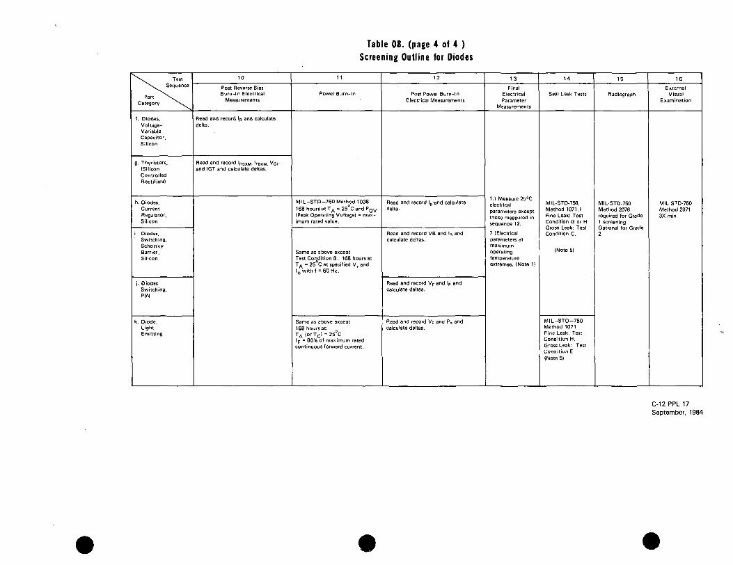
Table 08. (page 4 of 4 )Screening Outline for Diodes
^X. Test^•^ Sequence
Part ^s*\Category ^x.
f. Diodes,Voltage-VariableCapacitor,Silicon
g. Thyristors,(SiliconControlledRectifiers)
h. Diodes,CurrentRegulator,Silicon
i. Diodes,Switching,SchottkyBarrier,Silicon
j. DiodesSwitching,PIN
k. Diode,LightEmitting
10
Post Reverse BiasBurn-In Electrical
Measurements
Read and record IR and calculatedelta.
Read and record IHBXM, IFBXM, VGTand IGT and calculate deltas.
11
Power Burn-In
MIL-STD-750 Method 1038168 hours at TA - 25°C and PQV
(Peak Operating Voltage) = max-imum rated value.
Same as above exceptTest Condition B. 168 hours atTA = 25°C at specified Vr and10 withf • 60 Hz,
Same as above except168 hours at:TA (orTcl =25 CIp = 80% of maximum ratedcontinuous forward current.
12
Post Power Burn-InElectrical Measurements
Read and record lp-and calculatedelta.
Read and record VB and IR andcalculate deltas.
Read and record VF and IR andcalculate deltas.
Read and record VF and P0 andcalculate deltas.
13
FinalElectricalParameter
Measurements
1.) Measure 25°Celectricalparameters exceptthose measured insequence 12.
2. (Electricalparameters atmaximumoperatingtemperatureextremes. (Note 1)
14
Seal Leak Tests
MIL-STD-750,Method 1071.1Fine Leak: TestCondition G or H.
Condition C.
(Note 5}
MIL-STD-750Method 1071Fine Leak: TestCondition H.Gross Leak: TestCondition E(Note 5)
15
Radiograph
MIL-STD-750Method 2076required for' Grade1 screeningOptional for Grade2
16
ExternalVisual
Examination
MIL-STD-750Method 20713X min.
C-12 PPL 17September, 1984

Table 09. (page 1 of 4)
Screening Outline for Transistors1
\^ Test^\^ Sequence
Part ^^^Category ^-^
a. Transistors,Silicon, NPN,Low, Medium Power,Switching orGeneral Purpose
b. Transistors,Silicon, PNP,Low, MediumPower,Switching orGeneral Purpose
c. Transistors,Silicon, PNP,High Power
d. Transistors,Silicon, NPN,High Power
e. Transistors,Fie Id -Effect,Junction,N -Channel,Silicon
f. Transistors,Field-Effect,Junction,PrChannel,Silicon
1
Internal Visual(Precap) Inspection
MIL-STD-750 Method2072. (This test canonly be performed bythe manufacturer,when specified inprocurementdocument.)
2
Initial Inspection &Electrical Parameter
Measurements
1. Visual Inspectionper MIL-STD-750,Method 2071. 3Xmin.
2. Electricalparametermeasurements (Note1)
3
High TemperatureStorage
MIL-STD-750Method 1032
Store for 48 hours
(Note 2}
4
Thermal Shock(Temperature Cycling)
MIL-STD-202 Method107Test Condition C,except 10 cycles,except the maximumtemperature shall be125°C
5
Acceleration
MIL-STD-750 Method2006 except that testshall be 20,000 g in Y^orientation, onetime only. The 1 minhold-time requirementshall not apply.
Same as above except5,000 g.
Same as above except20,000 g.
6
PIND2
MIL-STD-750Method 2052
Only for Grade1 screening
(Note 3}
7
Seal Leak Tests
MIL-STD-750 Method1071. Fine Leak. TestCondition G or H. GrossLeak: Test Condition C.Only for Grade 2screening
(Note 4)
Same as above exceptfine leak rejectionvalue of 5 x 10 atmcc/sec. Only for Grade 2screening
MIL-STD-750 Method1071.1 Fine Leak: TestCondition G or H GrossLeak: Test Condition C.
Only for Grade 2screening
NOTES:1. Performance of electrical measurements at sequence 2 is optional. Measurements at high and low temperatures are also optional at this point;
however, if performed here they need not be performed at sequence 12. For Grade 1 applications, high and low temperature measurementsshall be made on all parts; whereas, LPTD sampling is permissible for Grade 2 applications.
2. Tests shall be conducted at the maximum operating temperature. If parts have leads that are not gold-plated they may be subject totarnishing at temperature greater than 125°C. Therefore, such parts must be tested in an inert atmosphere. After test, leads should beinspected for tarnishing, and refinished if necessary.
3. Particle Impact Noise Detection (PIND) shall be performed only on parts with internal package cavities.4. For Grade 2 applications, the seal leak tests may be performed at either test sequence 7 or 14. For Grade 1 applications, the tests must be
performed in test sequence 14; in addition, the test may be performed in test sequence 7.5. Reverse bias remains applied at the end of burn-in until TA reaches 30°C in test sequence 8.
C-13 PPL 17September, 1984

Table 09. (page 2 of 4)
Screening Outline for Transistors
^X. Test^•xSequence
Part ^\.Category ^X.
a. Transistors,Silicon, NPN,Low, MediumPower, Switchingor GeneralPurpose
b. Transistors,Silicon, PNP,Low, MediumPower, Switchingor General PurposePurpose
Silicon, PNP,High Power
d. Transistors,Silicon, NPN,High Power
e. Transistors,Field-Effect,Junction,N-Channel.Silicon
f. Transistors,Field-Effect,
-Junction,P-Channel,Silicon
8
Reverse Bias Burn-in(Notes 2, 5)
MIL-STD-750Method 1039
48 Hours at:Vpo = 80% of VponI E - 0
9
Pre-Burn-lnElectrical
Measurements
Read and recordICBO (or ICESand hFE.
Read and recordIGSS- 'DSSand IYf»l.
10
Burn-in(Notes 2, 5)
MIL-STD-750Method 1039168 hrs at specifiedVCB (or VCE)and PT (max.rated power dissipationat TA).
Same as above ex-cept Pj at casetemperaturespecified.
Same as above exceptat specified V^g andVDS-
11
Post Burn-In TestsMeasurements
Read and record ICBO andhFE and calculatedeltas.
Read and record IGSS, |DSS and IY,SLand calculate deltas.
12
FinalElectrical Parameter
Measurements
1.) Measure 25°Celectricalparameters exceptthose measured insequence 11 .
2.) Electricalparameters atmaximumoperatingtemperatureextremes.
(Note 1)
13
Seal Leak Tests(Note 4}
MIL-STD-750Method 1071.1. FineLeak: Test ConditionG orH Gross Leak:Test Condition C.
Only for Grade 1screening
Same as above exceptfine teak rejectionvalue 5 x 10 atmcc/sec. Only forGrade 1 screening
Same as aboveexcept Fine Leak: TestCondition G or HGross Leak: Test Con-dition C.
14
Radiography
MIL— STD— 750Method 2026Optional forGrade 2,Required forGrade 1
15
ExternalVisual
Examination
MIL— STD— 750Method 20723X min.
C-14 PPL 17September, 1984

Table 09. (page 3 of 4)
Screening Outline for Transistors1
^^^ Test^x. Sequence
Category ^s.
g. Transistors,Silicon,Unijunction
h. Transistors,Silicon,Chopper
i. Phototransistor
j. OpticallyCoupledIsolator
1
Internal Visual(Precap) Inspection
MIL-STD-750 Method2072. This test canonly be performedby the manufacturer.when specified inprocurement document.)
2
Initial Inspection &Electrical Parameter
Measurements
1. Visual Inspectionper MIL-STD-750Method 2071.3X mm.
2. Electricalparametermeasurements(Note 1)
3
High TemperatureStorage(Note 2)
MIL-STD-750Method 1032Store for 48 hours.
(Note 2)
4
Thermal Shock(Temperature Cycling)
MIL-STD-202 Method107 details.) TestConditions C, except10 cycles, except themaximum temperature
5
Acceleration
MIL-STD-750 Method2006 except that testshall be 20,000 g in YTorientation, one timeonly. The 1 min. hold-time requirement shallnot apply.
6
FIND2
MIL-STD-750Method 2052
Only for Grade 1screening
7
Seal Leak Tests(Note 4)
MIL-STD-750 Method1071.1. Fine Leak:Test Condition G or HGross Leak: TestCondition C. Only forGrade 2 screening.
MIL-STD-750 Method1071. Fine Leak: TestCondition H. Gross Leak:Test Condition C. Onlyfor Grade 2 Screening
MIL-STD-750 Method1071.1. Fine Leak: TestCondition G or H GrossLeak: Test Condition C.Only for Grade 2 Screening
o 2•n 5013 QO 2iP
m
C-15 PPL 17September, 1984

Table 09. (page 4 of 4)Screening Outline for Transistors
•̂s. Tesl•̂s. Sequence
Part ^x^Category ^x.
gl Transistors,Silicon,Unijunction
h. Transistors;Silicon,Chopper
, .
j. OpticallyCoupledIsolator
8
Reverse Bias Burn-in(Notes 2, 5)
MIL-STD-750 Method1039 48 Hours at: VCB =80% of VCBO U = 0
Same as above except48 hrs at:V C E =80%ofV C E O
Ee (Incident RadiantEnergy = 0)
Same as above exceptTest Condition A.
V C E =80%ofV C E O
gPre Burn-tn
ElectricalMeasurements
Read and record ltBTO
RBBOandri.
Read and record I ceoand hFE (inverted).
Rad and recordIQ and 1 1 .
Read and recordPhototransistor
IC (OFF)1C(ON)nFE
LED
'R
10
Burn-in(Note 2}
MIL-STD-750 Method1039
168 hrsat specified Vg2giand lg-|. (Maximumrated power.)
Same as above exceptat specified Vpp (orVC E) andPj. (Maxrated power dissi-pation at T A ) .
at specifiedVQE. Adjust Ee (inci-dent radiant energy)for PT = 80% of
device dissipation
Same as aboveexcept atmax. rated VCE.
PT = 80% of maxi-mum continousdevice dissipation
11
Post-Burn-InElectrical Measurements
Read and record 1EB20 RBBQ and nand calculate deltas.
Read and record ICBO and hFE (inverted) and calculatedeltas.
Read and record In and li and calculate deltas
Read Vlc (OFF), IC(ON), hFE, and IR and record andcalculate deltas.
12
FinalElectrical Parameter
Measurements
1.) Measure 25°Celectrical parametersexcept thosemeasured insequence 11,
2.) Electricalparameters ofmaximum operatingtemperatureextremes. (Note 11
13
Seal Leak Tests(Note 4)
MIL-STD-750Method 1071.1.Fine Leak: TestCondition G orH. Gross Leak:Test Condition C.
MIL— STD 750Method 1071Fine Leak: TestCondition H.Gross Leak:
C.
MIL-STD-750Method 1071.1Fine Leak: TestCondition G or HGross Leak: TestCondition C.
14
Radiography
MIL-STD-750Method 2026
Required forGrade 1
Optional forGrade2
15
ExternalVisual
Examination
MIL-STD-750Method 2072 3Xmin.
C-16 PPL 17September, 1984

Table 10.Screening Outline For Microcircuits
\ Screening
\
Grade \\
1
9
\ Screening\Sequence
Grade \^
1
2
1
Internal Visual(Precap)
Can only be per-formed by mfr.Specifyrequirement
MIL-STD-883Method 2010Condition A
Same as Grade 1
condition B
2
ElectricalMeasurements
(Note 1)
Same asGrade 1
y
Burn-In
MIL-STD-883Method 1015240hrs @ 125°C(Dynamic) Specify testcond. and burn-in cir-cuitry
Same as Grade 1 except160 hrs.
32
StabilizationBake
MIL-STD-883Method 1008condition C
Same asGrade 1
10
Interim ElectricalParameter
Measurements
Remeasure parametersspecified in step 8.Calculate delta and per-cent defective.
CMOS only
4
TemperatureCycling
MIL-STD-883Method 1010condition C,except the max-imum temperatureshall be 125°C.
Same asGrade 1
116.7
Reverse BiasBurn-In
MIL-STD 883Method 1015Condition A
Same as Grade 1
53
ConstantAcceleration
MIL-STD-883Method 2001condition E.Y Orientation only.
Same asGrade 1
125.8
Final ElectricalMeasurements
Measure DC, AC anddelta parameters @25 °C. Measure DCparameters @ min. andmax. operatingtemperatures.
Same as Grade 1
6
ParticleImpact Noise
Detection(PIND)
MIL-STD-883Method 2020Condition A.Lot acceptance permethod 2020
Same asGrade 1
13"
Radiographic
MIL-STD-883Method 2012
Not required
7"
Seal
MIL-STD-883Method 1014Fine Leak: cond. Aor B.Gross Leak: Cond.C.
Same asGrade 1
14
ExternalVisual
MIL-STD-883Method 2009
Same as Grade 1
85
InterimElectrical
ParameterMeasurements
Measure +25°CDC & ACparameters andrecord parametersrequiring deltacalculations
Same asGrade 1
NOTES:1. Performance of electrical measurements at this point is optional. However, if high and low measurements are
performed here, they need not be repeated in sequence 12. High and low temperature DC parameter measurementsshall be made on all parts. AC parameter measurements are only required at +25°C.
2. If parts have leads that are not gold-plated, they may be subject to tarnishing at temperatures greater than 125°C.Therefore, such parts must be tested in an inert atmosphere. After test, leads should be inspected for tarnishing,and refinished if necessary.
3. For microcircuit packages having an inner seal or cavity perimeter greater than 2 inches, or a mass greater than 5grams, refer to MIL-STD-883B, Method 5004, paragraph 3.2 for acceleration instructions.
4. Seal and radiographic tests may be performed in any sequence after PIND test.5. The parameter measurements and delta calculations required for both grade 1 & grade 2 screening shall include
those parameters and deltas (including measurements for each test condition for each parameter) specified in theMIL-M-38510 slash sheet for the selected part. If no slash sheet is available for the selected part, model theparameter and delta requirements from a slash sheet for a similar part type. If no slash sheet is available forselected or similar part types, consult the Parts Specialist for recommendations.
6. Screening sequence 11 not required except for CMOS parts. Also, for CMOS parts, a Static I and Static II burn-inis required per MIL-M-38510 for class S devices.
7. The order of the burn-ins for steps 9 and 11 is optional.8. Min. and Max. operating temperature parameter measurements are optional here if performed in sequence 2. C-17 PPL 17
September, 1984

Table 14.Screening Outline for Thermistors
"^X. Test^ •̂v. Sequence
Category ^\N^
(a) Thermistors,(ThermallySensitiveRegister)(NegativeTemp. Coef.)
(b) Thermistors,Fixed Silicon(PositiveTemp. Coef.)
1
ExternalVisual
Examination
MIL-T-23648Paragraph
4.6.1
2
InitialMeasurements
Zero-PowerResistance at25°C and IR
Zero-PowerResistance
at 25° C
3
Bake
1 00 hrs atMaximumSpecifiedOperating
Temperature
NotRequired
4
TemperatureCycle
MIL-STD-202Method 107
Cond. B
5
Burn-In
NotRequired
1.5 x rated pwr. for 96 hrs at 25°C
6
FinalMeasurements
and Tests
Zero-PowerResistanceat 25° C
7
ExternalVisual
Examination
MIL-T-23648Paragraph
4.6.1
C-18 PPL 17September, 1984

Table 15.Screening Outline for Transformers1
^\ Test^x^^ C
Category ^^^^
Transformers, Audioand Power
Transformers, Pulse,Low Power
1
Initial Measurements
1 . Visual Examination2. Dielectric Withstanding
Voltage (DWV)3. Induced Voltage4. Insulation Resistance (IR)5. D.C. Resistance (OCR)
of each winding6. Primary Inductance (L)
1 . Visual Examination2. Dielectric Withstanding
Voltage (DWV)3. Induced Voltage4. Insulation Resistance (IR)5. DC Resistance (OCR)6. Open Circuit Inductance
(OCL)7. Leakage Inductance8. Turns Ratio
2
Thermal Shock
MIL-STD-202, Method107, Test Condition A-l .Use maximum temperaturespecified for transformeras maximum temperature.
NotRequired
3
Burn-In
MIL-STD-981Par. 30.1.2.1.
MIL-T-21038Para. 4.7.4
4
Seal Leak Test
Do not perform thesetests on encapsulatedunits. MIL-STD-202,Method 112. TestCondition C for FineLeak. Test ConditionD for Gross Leak . Usemaximum temperaturespecified for transformeras bath temperature .
MIL-T-21038Para. 4.7.7(Gross Leak Test)
5
Final Measurementsand Delta Reject Criteria
Repeat initial examinationsand measurements.Reject;AL>±5%ADCR> ±5%
Repeat initial measurementsand examinations .Reject;ADCR> ±5%
D C
Documents
MIL-T-27
MIL-STD-202
MIL-STD-981
MIL-T-21038
C-19 PPL 17September, 1984

APPENDIX DRadiation Effects
The charged particles in the natural space environment pose a radiation risk to some elec-tronic parts, because when these particles pass through them, they can significantly degrade their:performance. Ground radiation tests on different electronic part types have indicated that whileparts like resistors and capacitors show no noticeable degradation, many microcircuits are verysensitive to ionizing radiation. In comparison with microcircuits, most discrete semiconductordevices — with some exceptions such as microwave and MOS transistors — show much lessdegradation. However, some transistors, particularly small signal types, are very susceptible toradiation induced failures when operated at low collector currents. Further, the radiation environ-ment seen by a device differs from one application to another depending upon the orbitparameters and upon location within the spacecraft, i.e., the equivalent shielding between it andthe outside environment. Therefore, while selecting electronic parts, it is necessary not only to con-sider the device hardness, but also the application and the projected radiation environment for theapplication.
In dealing with the natural space environment, designers have to be concerned with two typesof radiation damage, namely total dose effect and single event phenomena. The total dose effectis due to the cumulative ionization caused by the passage of all the ionizing particles through thedevice and is uniform over the device. This effect causes shifts in the threshold voltages of MOStransistors and can also decrease the carrier mobility in channels resulting in increased propagationdelay times. In bipolar devices, current gain and junction leakage currents are adversely affected.The extent of total dose damage depends not only on the total absorbed dose but also on the doserate and annealing characteristic of the device.
In contrast to the total dose effect, the single event upset is a localized effect which occurswhen a single heavy ion or proton of high energy causes logic upset in semiconductor devices con-taining memory cells. This type of error is called a "soft error" as it causes no permanent damageand the device can be reprogrammed for correct functioning. However, single heavy ions can alsocause latch-up, or hard errors, in devices with technologies where four layer SCR action is possi-ble. Once latch-up is initiated in a device, control and functionality are lost. Device destructionmay also result unless current is limited or power is turned off and on again.
The available radiation test data indicates that the radiation hardness of microcircuits can beexpected to vary not only with the device type and technology, but also with subtle process varia-tions continually being made by the manufacturers, i.e., with different manufacturing lots. Also,the radiation test results are strongly dependent upon the bias conditions and other details ofradiation testing, such as the dose rate and the nature of irradiating source. Furthermore, the samedevice type can be hard with respect to single event upsets while being soft to total dose effects orvice versa. All these factors make it very difficult to specify the hardness levels for a particularpart type and/or technology. However, in recent years a data base on the relative hardness of dif-ferent technologies to total dose and single event upsets has emerged from the radiation tests per-formed by different experimenters. Table 1 gives a comparison of the susceptibilities of differenttechnologies to the two types of natural radiation effects discussed above.
D-1 PPL 17September, 1984

Table 1. Comparison of Radiation Susceptibility forMicrocircuits of Different Technologies. 1
TechnologyTotal Dose2
Hardness LevelRads (Si) Soft Error
Relative Susceptibility3 To:
Latch-Up
DIGITAL
NMOS
CMOS/Bulk (unhardened)
CMOS/Bulk (hardened)
CMOS/SOS
TTL, Low Power TTL
Schottky TTL, Low PowerSchottky TTL
Advanced Low PowerSchottky TTL
5x10² - 104 High Immune
103 - 105 Moderate to high Moderate
2x10³ _ 1Q6 Low Low
103 - 105 Very low Immune
105 - 107 Low to High Low
105 - 107 Low to High None to Low
2x10⁴ - 106 — No Data Available —
I2L
ECL
LINEAR
CMOS
Bipolar, BI-FeT
2x10⁴ _ 106
£5x10⁶
103 _ 2x10⁷
6x10³'- 107
Moderate None too Low
Low None to Low
— No Data Available —
— No Data Available —
NOTES:
1. Refer to pages 10-1 and 10-2 for the technologies of different microcircuits listed in this PPL.
2. These figures define process averages. However, some devices may not meet these levels whileothers may exceed them, e.g. some Schottky TTL RAM's fail much below the lower limitlisted in the Table while most other devices with this technology fall within the range shown.
3. The single event susceptibility "ratings" listed here are relative to each other. However, a"moderate" error rate in a specific application may be unacceptably high if the application iscritical.
D-2 PPL 17September, 1984

Table 1 provides only a qualitative guideline of radiation sensitivity of microcircuits and isderived from published radiation test data.'. 2 This often may not be sufficient as the rapidchanges which have been occuring in microcircuit technology have been accompanied by changesin the radiation hardness of the parts. In general, lot sample testing may be necessary to determinethe hardness levels of a procured lot of devices prior to their usage in a particular application.However, it may be noted that a number of vendors are making efforts to qualify their parts tofour standard radiation levels: namely 2.5 K, 10 K, 100 K and 1 M rads. The parts qualified tothese levels are identified in MIL-specifications by the symbols, M, D, R and H respectively, in-serted in place of the slash mark in part markings. For more information and guidelines, consultthe radiation effects specialists listed in this PPL.
BIBLIOGRAPHY
1. "Microcircuit Radiation Data Bank", NTIS, Access # N83-27903.
2. Proceedings of IEEE Annual Conference on Nuclear and Space Radiation Effects, from 1977through 1983, published in the December issue of IEEE Transaction on Nuclear Science, vol.24 through Vol. 30.
D-3 PPL 17September, 1984

APPENDIX E
SCREENING VERIFICATION
All JANTXV semiconductors purchased to the requirements of MIL-S-19500 shall besubjected to the following 100% screening verification tests before use as Grade 2 parts. Thisrequirement shall not apply to JANS semiconductors. These tests may be used in lieu of theJANTXV rescreening requirements specified in MIL-STD-975. Screening verification shall alsobe performed on nonstandard JANTX and JANTXV parts.
1. External Visual
2. PIND
3. Fine Leak
4. Gross Leak
5. Initial Electrical
6. Power Burn-In orBurn-In per slash sheet
7. Post Burn-In Electrical
8. Delta Calculation
9. PDA
MIL-S-19500Requirement Paragraph
4.6.4.2
MIL-STD-750Test Method
2071
2052 (Condition A or B)
1071 Test Condition G, H
1071 Test Condition, A, C, E, F
as specified (25 °C only)
1039 (Transistors)1038 (Diodes)
as specified (25 °C only)
as specified
4.6.1
E-1 PPL 17September, 1984