gs9091b ds - semtech anc data checksum, and edh crc error detection and correction programmable anc...
TRANSCRIPT

GenLINX® II 270Mb/s Deserializer for SDI and DVB-ASI
GS9091B
Key Features• SMPTE 259M-C compliant descrambling and NRZI to
NRZ decoding (with bypass)
• DVB-ASI 8b/10b decoding
• Integrated Cable Equalizer
• 500m typical equalization of Belden 1694A cable
• Integrated line-based FIFO for data alignment/delay, clock phase interchange, DVB-ASI data packet extraction and clock rate interchange, and ancillary data packet extraction
• Integrated VCO and reclocker
• User selectable additional processing features including:
TRS, ANC data checksum, and EDH CRC error detection and correction
programmable ANC data detection
illegal code remapping
• Internal flywheel for noise immune H, V, F extraction
• Automatic standards detection and indication
• Enhanced Gennum Serial Peripheral Interface (GSPI)
• JTAG test interface
• Polarity insensitive for DVB-ASI and SMPTE signals
• +1.8V core power supply with optional +1.8V or +3.3V I/O power supply
• Small footprint (11mm x 11mm)
• Low power operation (typically 350mW)
• Pb-free and RoHS compliant
Applications• SMPTE 259M-C Serial Digital Interfaces
• DVB-ASI Serial Digital Interfaces
DescriptionThe GS9091B is a 270Mb/s equalizing and reclocking dese-rializer with an internal FIFO. It provides a complete re-ceive solution for SD-SDI and DVB-ASI applications.
In addition to equalizing, reclocking and deserializing the input data stream, the GS9091B performs NRZI -to-NRZ de-coding, descrambling as per SMPTE 259M-C, and word alignment when operating in SMPTE mode. When operat-ing in DVB-ASI mode, the device will word align the data to K28.5 sync characters and 8b/10b decode the received stream.
The integrated equalizer is optimized for 270Mb/s and can typically equalize up to 500m of Belden 1694A cable. Both the equalizer and the internal reclocker are fully compati-ble with both SMPTE and DVB-ASI input streams.
The GS9091B includes a range of data processing functions such as EDH support (error detection and handling), and automatic standards detection. The device can also detect and extract SMPTE 352M payload identifier packets and in-dependently identify the received video standard. This in-formation is read from internal registers via the host interface port.
The GS9091B also incorporates a video line-based FIFO. This FIFO may be used in four user-selectable modes to car-ry out tasks such as data alignment / delay, clock phase in-terchange, MPEG packet extraction and clock rate interchange, and ancillary data packet extraction.
Parallel data outputs are provided in 10-bit multiplexed format, with the associated parallel clock output signal op-erating at 27MHz.
The device may also be used in a low-latency data pass through mode where only descrambling and word align-ment will be performed in SMPTE mode.
1 of 73
Proprietary & Confidential
GS9091B GenLINX® II 270Mb/s Deserializer for SDI and DVB-ASIFinal Data Sheet 38910 - 3 February 2013
www.semtech.com
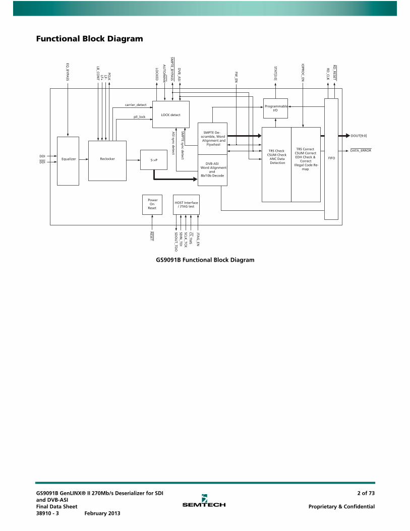
Functional Block Diagram
GS9091B Functional Block Diagram
Reclocker S->P
SMPTE De-scramble, WordAlignment and
Flywheel
DOUT[9:0]
carrier_detect
ASI syn
c detect
HOST Interface/ JTAG test
CS_TM
SSC
LK_TC
KSD
IN_TD
ISD
OU
T_TDO
DDI
DDI
DATA_ERROR
Power OnReset
JTAG
_EN
TRS CheckCSUM Check
ANC DataDetectionDVB-ASI
Word Alignmentand
8b/10b Decode
TRS CorrectCSUM CorrectEDH Check &
CorrectIllegal Code Re-
map
DV
B_A
SI
pll_lock
LF+LB
_CO
NT
PCLK
LOC
KED
LOCK detect
SMPTE_B
YPA
SS
SMPTE syn
c detect
LF-
AU
TO/M
AN
Programmable I/O
STAT[3:0]
FIFO
FW_EN
IOPR
OC
_EN
RD
_CLK
RD
_RESET
RESET
Equalizer
EQ_B
YPA
SS
GS9091B GenLINX® II 270Mb/s Deserializer for SDI and DVB-ASIFinal Data Sheet 38910 - 3 February 2013
2 of 73
Proprietary & Confidential
Revision History
Contents
Key Features ........................................................................................................................................................1
Applications.........................................................................................................................................................1
Description...........................................................................................................................................................1
Functional Block Diagram ..............................................................................................................................2
Revision History .................................................................................................................................................3
1. Pin Out...............................................................................................................................................................5
1.1 Pin Assignment ..................................................................................................................................5
2. Electrical Characteristics ......................................................................................................................... 12
2.1 DC Electrical Characteristics ..................................................................................................... 12
2.2 AC Electrical Characteristics ..................................................................................................... 14
2.3 Solder Reflow Profiles .................................................................................................................. 16
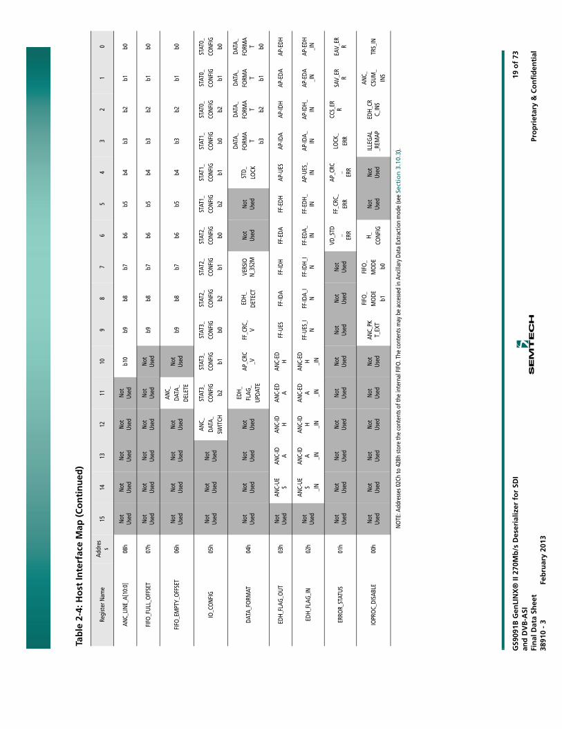
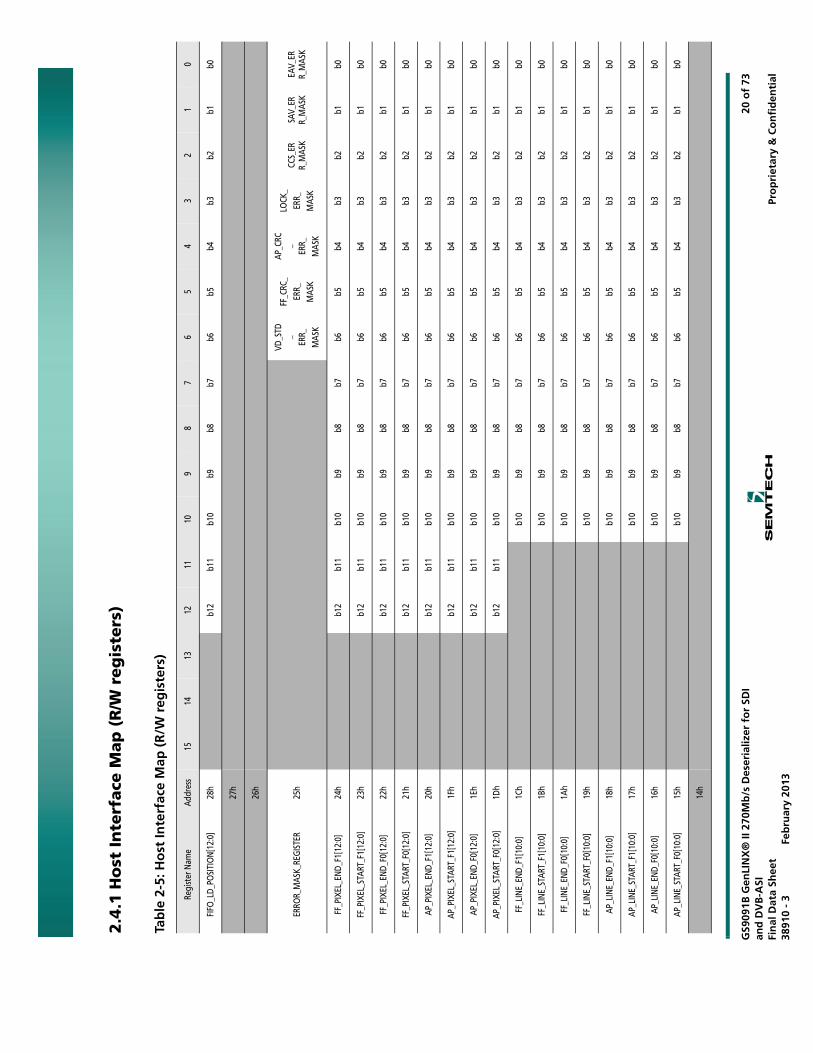
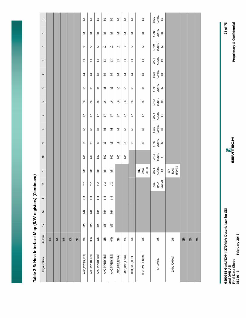
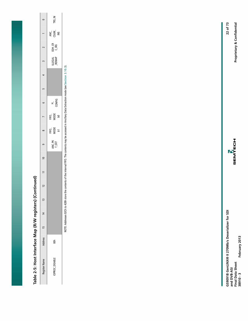
2.4 Host Interface Map ........................................................................................................................ 17
2.4.1 Host Interface Map (R/W registers) ............................................................................. 20
2.4.2 Host Interface Map (Read only registers) .................................................................. 23
3. Detailed Description.................................................................................................................................. 26
3.1 Functional Overview .................................................................................................................... 26
3.2 Cable Equalization ........................................................................................................................ 27
3.3 Clock and Data Recovery ............................................................................................................ 27
3.3.1 Internal VCO and Phase Detector................................................................................ 27
3.4 Serial-To-Parallel Conversion ................................................................................................... 27
3.5 Modes Of Operation ..................................................................................................................... 27
3.5.1 Lock Detect .......................................................................................................................... 28
3.5.2 Auto Mode............................................................................................................................ 29
3.5.3 Manual Mode ...................................................................................................................... 29
3.6 SMPTE Functionality .................................................................................................................... 30
3.6.1 SMPTE Descrambling and Word Alignment ............................................................ 30
3.6.2 Internal Flywheel .............................................................................................................. 30
3.6.3 Switch Line Lock Handling............................................................................................. 31
3.6.4 HVF Timing Signal Generation ..................................................................................... 32
3.7 DVB-ASI Functionality ................................................................................................................ 33
3.7.1 DVB-ASI 8b/10b Decoding............................................................................................. 34
Version ECO PCN Date Changes and/or Modifications
3 011367 – February 2013 Updated to the Semtech template.
2 150199 50711 July 2008 DVB_ASI operation specification change in Auto mode.
1 144807 – April 2007 Converting to Data Sheet. Modified Electrical Characteristics.
0 139930 – November 2006 New Document.
GS9091B GenLINX® II 270Mb/s Deserializer for SDI and DVB-ASIFinal Data Sheet 38910 - 3 February 2013
3 of 73
Proprietary & Confidential
3.7.2 Status Signal Outputs ....................................................................................................... 34
3.8 Data-Through Functionality ...................................................................................................... 34
3.9 Additional Processing Features ................................................................................................ 35
3.9.1 FIFO Load Pulse ................................................................................................................. 35
3.9.2 Ancillary Data Detection and Indication................................................................... 36
3.9.3 EDH Packet Detection...................................................................................................... 37
3.9.4 EDH Flag Detection........................................................................................................... 38
3.9.5 SMPTE 352M Payload Identifier................................................................................... 41
3.9.6 Automatic Video Standard and Data Format Detection ...................................... 42
3.9.7 Error Detection and Indication ..................................................................................... 43
3.9.8 Additional SMPTE Mode Processing ........................................................................... 48
3.10 Internal FIFO Operation ........................................................................................................... 51
3.10.1 Video Mode ....................................................................................................................... 51
3.10.2 DVB-ASI Mode ................................................................................................................. 53
3.10.3 Ancillary Data Extraction Mode ................................................................................ 56
3.10.4 Bypass Mode..................................................................................................................... 58
3.11 Parallel Data Outputs ................................................................................................................. 59
3.11.1 Parallel Data Bus Output Buffers ............................................................................... 59
3.11.2 Parallel Output in SMPTE Mode................................................................................. 60
3.11.3 Parallel Output in DVB-ASI Mode............................................................................. 60
3.11.4 Parallel Output in Data-Through Mode................................................................... 60
3.12 Programmable Multi-Function Outputs .............................................................................. 60
3.13 GS9091B Low-latency Mode ................................................................................................... 62
3.14 GSPI Host Interface ..................................................................................................................... 63
3.14.1 Command Word Description ...................................................................................... 63
3.14.2 Data Read and Write Timing ....................................................................................... 64
3.14.3 Configuration and Status Registers........................................................................... 66
3.15 JTAG operation ............................................................................................................................ 67
3.16 Device Power Up ......................................................................................................................... 68
4. References & Relevant Standards ......................................................................................................... 69
5. Application Information .......................................................................................................................... 70
5.1 Typical Application Circuit ........................................................................................................ 70
6. Package & Ordering Information .......................................................................................................... 71
6.1 Package Dimensions ..................................................................................................................... 71
6.2 Packaging Data ............................................................................................................................... 72
6.3 Marking Diagram ........................................................................................................................... 72
6.4 Ordering Information ................................................................................................................... 72
GS9091B GenLINX® II 270Mb/s Deserializer for SDI and DVB-ASIFinal Data Sheet 38910 - 3 February 2013
4 of 73
Proprietary & Confidential

1. Pin Out
1.1 Pin Assignment
Figure 1-1: Pin Assignment
1 32 4 5 6 7 8 9 10
A
B
C
D
E
F
G
H
J
K
LOCKED PCLK LB_CONT
VBG DOUT9
DOUT8
DOUT0
DOUT7
DOUT6
DOUT5
DOUT4
DOUT2
DOUT1JTAG_EN
IO_VDD
IO_VDD
IO_GND
IO_VDD
CORE_VDD
CORE_GND
CORE_GND
DATA_
ERROR
FW_EN DVB_ASISMPTE_BYPASS
NC
HEAT_SINK_GND
SDIN_TDI
SCLK_TCK
SDOUT_TDO
CS_TMS
NC
NC
NC
NCANA_VDD
NCNC NC
NCTERM
SDI
IOPROC_EN RESET
VCO_VDD
LF+
PLL_VDD
EQ_GND
AGC+
RD_CLK
STAT2
NC
NC FIFO_EN AUTO/MAN
LF-PLL_GND
VCO_GND
ANA_VDD NC NC
ANA_GND
ANA_GND
IO_GND
IO_GNDCORE_GND
CORE_GND
IO_GND
HEAT_SINK_GND
IO_GNDCORE_GND
IO_GND IO_VDDNCCORE_GND
DOUT3HEAT_SINK_GND
SDIHEAT_SINK_GND
IO_GNDCORE_GND
IO_GND NCCORE_GND
NC
EQ_VDDHEAT_SINK_GND
HEAT_SINK_GND
NCNC NC NC RD_RESET
EQ_BYPASS
CORE_VDD
STAT3
AGC- NC STAT0 STAT1
GS9091B GenLINX® II 270Mb/s Deserializer for SDI and DVB-ASIFinal Data Sheet 38910 - 3 February 2013
5 of 73
Proprietary & Confidential
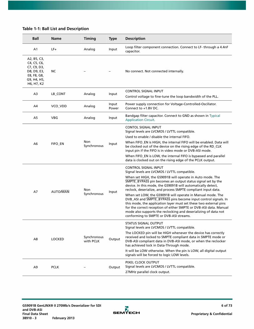
Table 1-1: Ball List and Description
Ball Name Timing Type Description
A1 LF+ Analog InputLoop filter component connection. Connect to LF- through a 4.4nF capacitor.
A2, B5, C3, C4, C5, C6, C7, C9, D3, D8, D9, E3, E8, F8, G8, G9, H4, H5, H6, H7, K2
NC – – No connect. Not connected internally.
A3 LB_CONT Analog InputCONTROL SIGNAL INPUT
Control voltage to fine-tune the loop bandwidth of the PLL.
A4 VCO_VDD AnalogInput Power
Power supply connection for Voltage-Controlled-Oscillator. Connect to +1.8V DC.
A5 VBG Analog InputBandgap filter capacitor. Connect to GND as shown in Typical Application Circuit.
A6 FIFO_ENNon Synchronous
Input
CONTOL SIGNAL INPUT Signal levels are LVCMOS / LVTTL compatible.
Used to enable / disable the internal FIFO.
When FIFO_EN is HIGH, the internal FIFO will be enabled. Data will be clocked out of the device on the rising edge of the RD_CLK input pin if the FIFO is in video mode or DVB-ASI mode.
When FIFO_EN is LOW, the internal FIFO is bypassed and parallel data is clocked out on the rising edge of the PCLK output.
A7 AUTO/MANNon Synchronous
Input
CONTROL SIGNAL INPUT Signal levels are LVCMOS / LVTTL compatible.
When set HIGH, the GS9091B will operate in Auto mode. The SMPTE_BYPASS pin becomes an output status signal set by the device. In this mode, the GS9091B will automatically detect, reclock, deserialize, and process SMPTE compliant input data.
When set LOW, the GS9091B will operate in Manual mode. The DVB_ASI and SMPTE_BYPASS pins become input control signals. In this mode, the application layer must set these two external pins for the correct reception of either SMPTE or DVB-ASI data. Manual mode also supports the reclocking and deserializing of data not conforming to SMPTE or DVB-ASI streams.
A8 LOCKEDSynchronous with PCLK
Output
STATUS SIGNAL OUTPUT Signal levels are LVCMOS / LVTTL compatible.
The LOCKED pin will be HIGH whenever the device has correctly received and locked to SMPTE compliant data in SMPTE mode or DVB-ASI compliant data in DVB-ASI mode, or when the reclocker has achieved lock in Data-Through mode.
It will be LOW otherwise. When the pin is LOW, all digital output signals will be forced to logic LOW levels.
A9 PCLK – OutputPIXEL CLOCK OUTPUT Signal levels are LVCMOS / LVTTL compatible.
27MHz parallel clock output.
GS9091B GenLINX® II 270Mb/s Deserializer for SDI and DVB-ASIFinal Data Sheet 38910 - 3 February 2013
6 of 73
Proprietary & Confidential
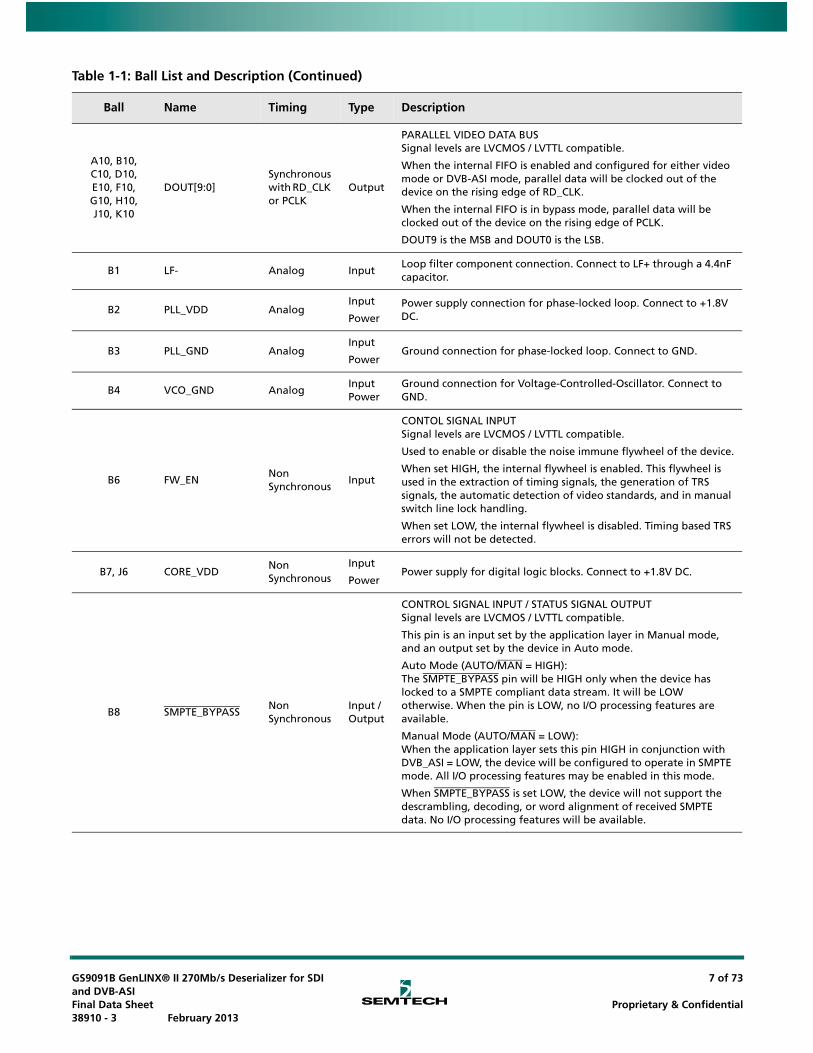
A10, B10, C10, D10, E10, F10, G10, H10, J10, K10
DOUT[9:0]Synchronous with RD_CLK or PCLK
Output
PARALLEL VIDEO DATA BUS Signal levels are LVCMOS / LVTTL compatible.
When the internal FIFO is enabled and configured for either video mode or DVB-ASI mode, parallel data will be clocked out of the device on the rising edge of RD_CLK.
When the internal FIFO is in bypass mode, parallel data will be clocked out of the device on the rising edge of PCLK.
DOUT9 is the MSB and DOUT0 is the LSB.
B1 LF- Analog InputLoop filter component connection. Connect to LF+ through a 4.4nF capacitor.
B2 PLL_VDD AnalogInput
PowerPower supply connection for phase-locked loop. Connect to +1.8V DC.
B3 PLL_GND AnalogInput
PowerGround connection for phase-locked loop. Connect to GND.
B4 VCO_GND AnalogInput Power
Ground connection for Voltage-Controlled-Oscillator. Connect to GND.
B6 FW_ENNon Synchronous
Input
CONTOL SIGNAL INPUT Signal levels are LVCMOS / LVTTL compatible.
Used to enable or disable the noise immune flywheel of the device.
When set HIGH, the internal flywheel is enabled. This flywheel is used in the extraction of timing signals, the generation of TRS signals, the automatic detection of video standards, and in manual switch line lock handling.
When set LOW, the internal flywheel is disabled. Timing based TRS errors will not be detected.
B7, J6 CORE_VDDNon Synchronous
Input
PowerPower supply for digital logic blocks. Connect to +1.8V DC.
B8 SMPTE_BYPASSNon Synchronous
Input / Output
CONTROL SIGNAL INPUT / STATUS SIGNAL OUTPUT Signal levels are LVCMOS / LVTTL compatible.
This pin is an input set by the application layer in Manual mode, and an output set by the device in Auto mode.
Auto Mode (AUTO/MAN = HIGH): The SMPTE_BYPASS pin will be HIGH only when the device has locked to a SMPTE compliant data stream. It will be LOW otherwise. When the pin is LOW, no I/O processing features are available.
Manual Mode (AUTO/MAN = LOW): When the application layer sets this pin HIGH in conjunction with DVB_ASI = LOW, the device will be configured to operate in SMPTE mode. All I/O processing features may be enabled in this mode.
When SMPTE_BYPASS is set LOW, the device will not support the descrambling, decoding, or word alignment of received SMPTE data. No I/O processing features will be available.
Table 1-1: Ball List and Description (Continued)
Ball Name Timing Type Description
GS9091B GenLINX® II 270Mb/s Deserializer for SDI and DVB-ASIFinal Data Sheet 38910 - 3 February 2013
7 of 73
Proprietary & Confidential
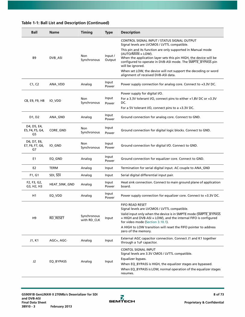
B9 DVB_ASINon Synchronous
Input / Output
CONTROL SIGNAL INPUT / STATUS SIGNAL OUTPUT Signal levels are LVCMOS / LVTTL compatible.
This pin and its function are only supported in Manual mode (AUTO/MAN = LOW). When the application layer sets this pin HIGH, the device will be configured to operate in DVB-ASI mode. The SMPTE_BYPASS pin will be ignored.
When set LOW, the device will not support the decoding or word alignment of received DVB-ASI data.
C1, C2 ANA_VDD AnalogInput Power
Power supply connection for analog core. Connect to +3.3V DC.
C8, E9, F9, H8 IO_VDDNon Synchronous
Input
Power
Power supply for digital I/O.
For a 3.3V tolerant I/O, connect pins to either +1.8V DC or +3.3V DC.
For a 5V tolerant I/O, connect pins to a +3.3V DC.
D1, D2 ANA_GND AnalogInput Power
Ground connection for analog core. Connect to GND.
D4, D5, E4, E5, F4, F5, G4,
G5CORE_GND
Non Synchronous
Input
PowerGround connection for digital logic blocks. Connect to GND.
D6, D7, E6, E7, F6, F7, G6,
G7IO_GND
Non Synchronous
Input Power
Ground connection for digital I/O. Connect to GND.
E1 EQ_GND AnalogInput Power
Ground connection for equalizer core. Connect to GND.
E2 TERM Analog Input Termination for serial digital input. AC couple to ANA_GND
F1, G1 SDI, SDI Analog Input Serial digital differential input pair.
F2, F3, G2, G3, H2, H3
HEAT_SINK_GND AnalogInput Power
Heat sink connection. Connect to main ground plane of application board.
H1 EQ_VDD AnalogInput Power
Power supply connection for equalizer core. Connect to +3.3V DC.
H9 RD_RESETSynchronous with RD_CLK
Input
FIFO READ RESET Signal levels are LVCMOS / LVTTL compatible.
Valid input only when the device is in SMPTE mode (SMPTE_BYPASS = HIGH and DVB-ASI = LOW), and the internal FIFO is configured for video mode (Section 3.10.1).
A HIGH to LOW transition will reset the FIFO pointer to address zero of the memory.
J1, K1 AGC+, AGC- Analog InputExternal AGC capacitor connection. Connect J1 and K1 together through a 1uF capacitor.
J2 EQ_BYPASS Analog Input
CONTOL SIGNAL INPUT Signal levels are 3.3V CMOS / LVTTL compatible.
Equalizer bypass.
When EQ_BYPASS is HIGH, the equalizer stages are bypassed.
When EQ_BYPASS is LOW, normal operation of the equalizer stages resumes.
Table 1-1: Ball List and Description (Continued)
Ball Name Timing Type Description
GS9091B GenLINX® II 270Mb/s Deserializer for SDI and DVB-ASIFinal Data Sheet 38910 - 3 February 2013
8 of 73
Proprietary & Confidential

J3 JTAG_ENNon Synchronous
Input
CONTROL SIGNAL INPUT Signal levels are LVCMOS / LVTTL compatible.
Used to select JTAG Test Mode or Host Interface Mode.
When set HIGH, CS_TMS, SCLK_TCK, SDOUT_TDO, and SDIN_TDI are configured for JTAG boundary scan testing.
When set LOW, CS_TMS, SCLK_TCK, SDOUT_TDO, and SDIN_TDI are configured as GSPI pins for normal host interface operation.
J4 CS_TMSSynchronous with SCLK_TCK
Input
CONTROL SIGNAL INPUT Signal levels are LVCMOS / LVTTL compatible.
Chip Select / Test Mode Select
Host Mode (JTAG_EN = LOW): CS_TMS operates as the host interface chip select, CS, and is active LOW.
JTAG Test Mode (JTAG_EN = HIGH): CS_TMS operates as the JTAG test mode select, TMS, and is active HIGH.
J5 SDOUT_TDOSynchronous with SCLK_TCK
Output
CONTROL SIGNAL INPUT Signal levels are LVCMOS / LVTTL compatible.
Serial Data Output / Test Data Output
Host Mode (JTAG_EN = LOW): SDOUT_TDO operates as the host interface serial output, SDOUT, used to read status and configuration information from the internal registers of the device.
JTAG Test Mode (JTAG_EN = HIGH): SDOUT_TDO operates as the JTAG test data output, TDO.
J7 DATA_ERRORSynchronous with PCLK
Output
STATUS SIGNAL OUTPUT. Signal levels are LVCMOS / LVTTL compatible.
The DATA_ERROR pin will be LOW when an error within the received data stream has been detected by the device. This pin is an inverted logical OR-ing of all detectable errors listed in the internal ERROR_STATUS register.
Once an error is detected, DATA_ERROR will remain LOW until the start of the next video frame / field, or until the ERROR_STATUS register is read via the host interface.
The DATA_ERROR pin will be HIGH when the received data stream has been detected without error.
NOTE: It is possible to program which error conditions are monitored by the device by setting appropriate bits in the ERROR_MASK register HIGH. All error conditions are detected by default.
Table 1-1: Ball List and Description (Continued)
Ball Name Timing Type Description
GS9091B GenLINX® II 270Mb/s Deserializer for SDI and DVB-ASIFinal Data Sheet 38910 - 3 February 2013
9 of 73
Proprietary & Confidential
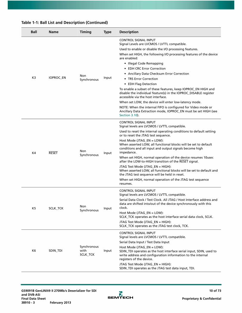
K3 IOPROC_ENNon Synchronous
Input
CONTROL SIGNAL INPUT Signal Levels are LVCMOS / LVTTL compatible.
Used to enable or disable the I/O processing features.
When set HIGH, the following I/O processing features of the device are enabled:
• Illegal Code Remapping
• EDH CRC Error Correction
• Ancillary Data Checksum Error Correction
• TRS Error Correction
• EDH Flag Detection
To enable a subset of these features, keep IOPROC_EN HIGH and disable the individual feature(s) in the IOPROC_DISABLE register accessible via the host interface.
When set LOW, the device will enter low-latency mode.
NOTE: When the internal FIFO is configured for Video mode or Ancillary Data Extraction mode, IOPROC_EN must be set HIGH (see Section 3.10).
K4 RESETNon Synchronous
Input
CONTROL SIGNAL INPUT Signal levels are LVCMOS / LVTTL compatible.
Used to reset the internal operating conditions to default setting or to reset the JTAG test sequence.
Host Mode (JTAG_EN = LOW): When asserted LOW, all functional blocks will be set to default conditions and all input and output signals become high impedance.
When set HIGH, normal operation of the device resumes 10usec after the LOW-to-HIGH transition of the RESET signal.
JTAG Test Mode (JTAG_EN = HIGH): When asserted LOW, all functional blocks will be set to default and the JTAG test sequence will be held in reset.
When set HIGH, normal operation of the JTAG test sequence resumes.
K5 SCLK_TCKNon Synchronous
Input
CONTROL SIGNAL INPUT Signal levels are LVCMOS / LVTTL compatible.
Serial Data Clock / Test Clock. All JTAG / Host Interface address and data are shifted into/out of the device synchronously with this clock.
Host Mode (JTAG_EN = LOW): SCLK_TCK operates as the host interface serial data clock, SCLK.
JTAG Test Mode (JTAG_EN = HIGH): SCLK_TCK operates as the JTAG test clock, TCK.
K6 SDIN_TDISynchronous with SCLK_TCK
Input
CONTROL SIGNAL INPUT Signal levels are LVCMOS / LVTTL compatible.
Serial Data Input / Test Data Input
Host Mode (JTAG_EN = LOW): SDIN_TDI operates as the host interface serial input, SDIN, used to write address and configuration information to the internal registers of the device.
JTAG Test Mode (JTAG_EN = HIGH): SDIN_TDI operates as the JTAG test data input, TDI.
Table 1-1: Ball List and Description (Continued)
Ball Name Timing Type Description
GS9091B GenLINX® II 270Mb/s Deserializer for SDI and DVB-ASIFinal Data Sheet 38910 - 3 February 2013
10 of 73
Proprietary & Confidential
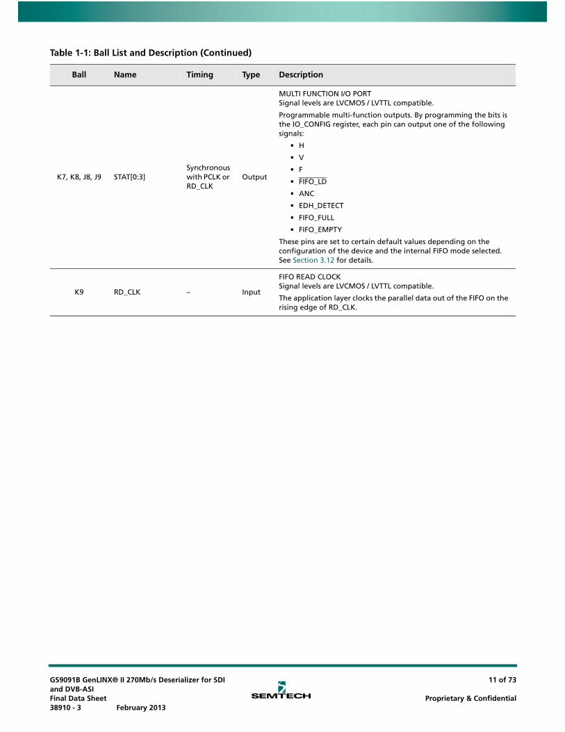
K7, K8, J8, J9 STAT[0:3]Synchronous with PCLK or RD_CLK
Output
MULTI FUNCTION I/O PORT Signal levels are LVCMOS / LVTTL compatible.
Programmable multi-function outputs. By programming the bits is the IO_CONFIG register, each pin can output one of the following signals:
• H
• V
• F
• FIFO_LD
• ANC
• EDH_DETECT
• FIFO_FULL
• FIFO_EMPTY
These pins are set to certain default values depending on the configuration of the device and the internal FIFO mode selected. See Section 3.12 for details.
K9 RD_CLK – Input
FIFO READ CLOCK Signal levels are LVCMOS / LVTTL compatible.
The application layer clocks the parallel data out of the FIFO on the rising edge of RD_CLK.
Table 1-1: Ball List and Description (Continued)
Ball Name Timing Type Description
GS9091B GenLINX® II 270Mb/s Deserializer for SDI and DVB-ASIFinal Data Sheet 38910 - 3 February 2013
11 of 73
Proprietary & Confidential

2. Electrical Characteristics
2.1 DC Electrical Characteristics
Table 2-1: Absolute Maximum Ratings
Parameter Value/Units
Supply Voltage Core -0.3V to +2.1V
Supply Voltage I/O -0.3V to +3.47V
Input Voltage Range (LF+, LF-, LB_CONT, VBG) -0.5V to +2.3V
Input Voltage Range (SDI, SDI, AGC+, AGC-, EQ_BYPASS) -0.5V to +3.6V
Input Voltage Range (All Other) -0.5V to +5.25V
Ambient Operating Temperature -20°C < TA < 85°C
Storage Temperature -40°C < TSTG < 125°C
ESD protection on all pins (see Note 1) 1kV
Notes:
1. MIL STD 883 ESD protection will be applied to all pins on the device.
2. Absolute Maximum Ratings are those values beyond which damage to the device may occur. Functional operation under these conditions or at any other condition beyond those indicated in the AC/DC Electrical Characteristic sections is not implied.
Table 2-2: DC Electrical Characteristics
VDD = 1.8V ±5%, 3.3V ±5%; TA = 0°C to 70°C, unless otherwise specified. Typical values: VCC = 1.8V, 3.3V and TA =25°C
Parameter Symbol Condition Min Typ Max Units Notes
System
Operating Temperature Range TA – 0 25 70 °C 1
Core Power Supply Voltage CORE_VDD – 1.71 1.8 1.89 V –
Analog Core Power Supply Voltage ANA_VDD – 3.13 3.3 3.47 V –
Digital I/O Buffer Power Supply Voltage
IO_VDD 1.8V Operation 1.71 1.8 1.89 V –
IO_VDD 3.3V Operation 3.13 3.3 3.47 V –
PLL Power Supply Voltage PLL_VDD – 1.71 1.8 1.89 V –
VCO Power Supply Voltage VCO_VDD – 1.71 1.8 1.89 V –
Equalizer Power Supply Voltage EQ_VDD – 3.13 3.3 3.47 V –
Core Supply Current IDDTotal 1.8V Supply – 64 80 mA 2
Total 3.3V Supply – 69 92 mA 3
GS9091B GenLINX® II 270Mb/s Deserializer for SDI and DVB-ASIFinal Data Sheet 38910 - 3 February 2013
12 of 73
Proprietary & Confidential
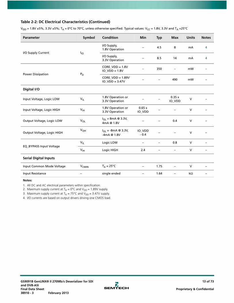
I/O Supply Current IIO
I/O Supply, 1.8V Operation
– 4.5 8 mA 4
I/O Supply, 3.3V Operation
– 8.5 14 mA 4
Power Dissipation PD
CORE_VDD = 1.8V IO_VDD = 1.8V
– 350 – mW –
CORE_VDD = 1.89V IO_VDD = 3.47V
– – 490 mW –
Digital I/O
Input Voltage, Logic LOW VIL1.8V Operation or 3.3V Operation
– –0.35 x
IO_VDDV –
Input Voltage, Logic HIGH VIH1.8V Operation or 3.3V Operation
0.65 x IO_VDD
– – V –
Output Voltage, Logic LOW VOLIOL = 8mA @ 3.3V, 4mA @ 1.8V
– – 0.4 V –
Output Voltage, Logic HIGHVOH IOL = -8mA @ 3.3V,
-4mA @ 1.8VIO_VDD
- 0.4– – V –
EQ_BYPASS Input VoltageVIL Logic LOW – – 0.8 V –
VIH Logic HIGH 2.4 – – V –
Serial Digital Inputs
Input Common Mode Voltage VCMIN TA = 25°C – 1.75 – V –
Input Resistance – single ended – 1.64 – kΩ –
Notes:
1. All DC and AC electrical parameters within specification.2. Maximum supply current at TA = 0°C and VDD = 1.89V supply.3. Maximum supply current at TA = 75°C and VDD = 3.47V supply.4. I/O currents are based on output drivers driving one CMOS load.
Table 2-2: DC Electrical Characteristics (Continued)
VDD = 1.8V ±5%, 3.3V ±5%; TA = 0°C to 70°C, unless otherwise specified. Typical values: VCC = 1.8V, 3.3V and TA =25°C
Parameter Symbol Condition Min Typ Max Units Notes
GS9091B GenLINX® II 270Mb/s Deserializer for SDI and DVB-ASIFinal Data Sheet 38910 - 3 February 2013
13 of 73
Proprietary & Confidential
2.2 AC Electrical Characteristics
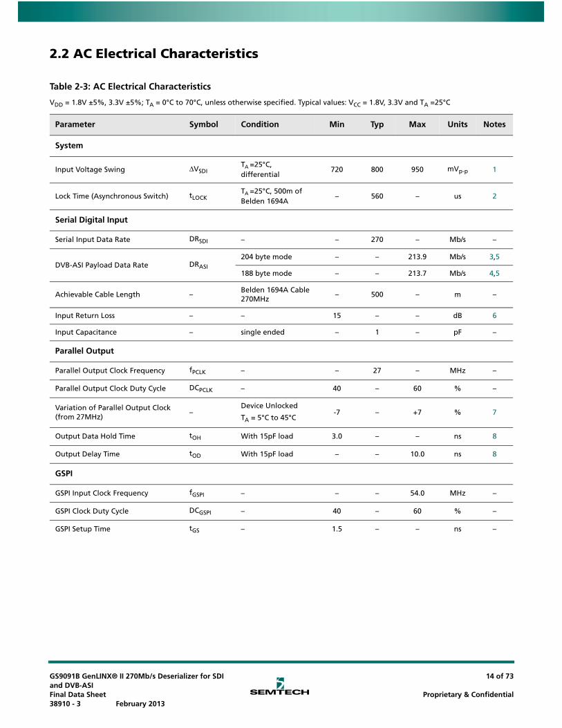
Table 2-3: AC Electrical Characteristics
VDD = 1.8V ±5%, 3.3V ±5%; TA = 0°C to 70°C, unless otherwise specified. Typical values: VCC = 1.8V, 3.3V and TA =25°C
Parameter Symbol Condition Min Typ Max Units Notes
System
Input Voltage Swing ΔVSDITA =25°C, differential
720 800 950 mVp-p 1
Lock Time (Asynchronous Switch) tLOCKTA =25°C, 500m of Belden 1694A
– 560 – us 2
Serial Digital Input
Serial Input Data Rate DRSDI – – 270 – Mb/s –
DVB-ASI Payload Data Rate DRASI
204 byte mode – – 213.9 Mb/s 3,5
188 byte mode – – 213.7 Mb/s 4,5
Achievable Cable Length –Belden 1694A Cable 270MHz
– 500 – m –
Input Return Loss – – 15 – – dB 6
Input Capacitance – single ended – 1 – pF –
Parallel Output
Parallel Output Clock Frequency fPCLK – – 27 – MHz –
Parallel Output Clock Duty Cycle DCPCLK – 40 – 60 % –
Variation of Parallel Output Clock (from 27MHz)
–Device Unlocked
TA = 5°C to 45°C-7 – +7 % 7
Output Data Hold Time tOH With 15pF load 3.0 – – ns 8
Output Delay Time tOD With 15pF load – – 10.0 ns 8
GSPI
GSPI Input Clock Frequency fGSPI – – – 54.0 MHz –
GSPI Clock Duty Cycle DCGSPI – 40 – 60 % –
GSPI Setup Time tGS – 1.5 – – ns –
GS9091B GenLINX® II 270Mb/s Deserializer for SDI and DVB-ASIFinal Data Sheet 38910 - 3 February 2013
14 of 73
Proprietary & Confidential

GSPI Hold Time tGH – 1.5 – – ns –
Notes:
1. 0m cable length.2. Time from input no-data to data switch and LOCKED pin set HIGH.3. Transmission format includes 204 byte data packets preceded by two K28.5 synchronization characters. Payload data rate excludes the two
K28.5 synchronization characters.4. Transmission format includes 188 byte data packets preceded by two K28.5 synchronization characters. Payload data rate excludes the two
K28.5 synchronization characters.5. Maximum payload is achieved via data packet mode, however, any combination of burst and packet mode is supported as long as each byte
or packet is preceded by two K28.5 characters.6. 5MHz to 270MHz.7. When the serial input to the GS9091B is removed, the PCLK output signal will continue to operate at 27MHz and the internal VCO will remain
at this frequency within +/-7% over the range 5oC to 45oC. Over the full operating temperature range (0oC to 70oC), the VCO may deviate from 27MHz up to +/-13%.
8. Timing includes the following outputs: DOUT[9:0], H, V, F, ANC, EDH_DETECT, FIFO_FULL, FIFO_EMPTY, FIFO_LD, WORDERR, SYNCOUT. When the FIFO is enabled, the outputs are measured with respect to RD_CLK.
Table 2-3: AC Electrical Characteristics (Continued)
VDD = 1.8V ±5%, 3.3V ±5%; TA = 0°C to 70°C, unless otherwise specified. Typical values: VCC = 1.8V, 3.3V and TA =25°C
Parameter Symbol Condition Min Typ Max Units Notes
GS9091B GenLINX® II 270Mb/s Deserializer for SDI and DVB-ASIFinal Data Sheet 38910 - 3 February 2013
15 of 73
Proprietary & Confidential

2.3 Solder Reflow ProfilesThe device is manufactured with Matte-Sn terminations and is compatible with both standard eutectic and Pb-free solder reflow profiles. MSL qualification was performed using the maximum Pb-free reflow profile shown in Figure 2-1. The recommended standard eutectic reflow profile is shown in Figure 2-2.
Figure 2-1: Maximum Pb-free Solder Reflow Profile (Preferred)
Figure 2-2: Standard Eutectic Solder Reflow Profile
25°C
150°C
200°C
217°C
260°C250°C
Time
Temperature
8 min. max
60-180 sec. max
60-150 sec.
20-40 sec.
3°C/sec max
6°C/sec max
25°C
100°C
150°C
183°C
230°C220°C
Time
Temperature
6 min. max
120 sec. max
60-150 sec.
10-20 sec.
3°C/sec max
6°C/sec max
GS9091B GenLINX® II 270Mb/s Deserializer for SDI and DVB-ASIFinal Data Sheet 38910 - 3 February 2013
16 of 73
Proprietary & Confidential
GS9
091B
Gen
LIN
X®
II 2
70M
b/s
Des
eria
lizer
fo
r SD
I an
d D
VB
-ASI
Fin
al D
ata
Shee
t
3891
0 -
3Fe
bru
ary
2013
17 o
f 73
Pro
pri
etar
y &
Co
nfi
den
tial
R K
2.4
Ho
st I
nte
rface
Map
Tab
le 2
-4: H
ost
Inte
rfac
e M
ap
Regi
ster
Nam
eAd
dres
s15
1413
1211
109
87
65
43
21
0
FIFO
_LD_
POSI
TIO
N[12
:0]
28h
Not
Used
Not
Used
Not
Used
b12
b11
b10
b9b8
b7b6
b5b4
b3b2
b1b0
27h
26h
ERRO
R_M
ASK_
REGI
STER
25h
Not
Used
Not
Used
Not
Used
Not
Used
Not
Used
Not
Used
Not
Used
Not
Used
Not
Used
VD_S
TD_
ERR_
MAS
K
FF_C
RC_
ERR_
MAS
K
AP_C
RC_
ERR_
MAS
K
LOCK
_ER
R_M
ASK
CCS_
ERR_
MAS
KSA
V_ER
R_M
ASK
EAV_
ER_
MAS
FF_P
IXEL
_END
_F1[
12:0
]24
hNo
t Us
edNo
t Us
edNo
t Us
edb1
2b1
1b1
0b9
b8b7
b6b5
b4b3
b2b1
b0
FF_P
IXEL
_STA
RT_F
1[12
:0]
23h
Not
Used
Not
Used
Not
Used
b12
b11
b10
b9b8
b7b6
b5b4
b3b2
b1b0
FF_P
IXEL
_END
_F0[
12:0
]22
hNo
t Us
edNo
t Us
edNo
t Us
edb1
2b1
1b1
0b9
b8b7
b6b5
b4b3
b2b1
b0
FF_P
IXEL
_STA
RT_F
0[12
:0]
21h
Not
Used
Not
Used
Not
Used
b12
b11
b10
b9b8
b7b6
b5b4
b3b2
b1b0
AP_P
IXEL
_END
_F1[
12:0
]20
hNo
t Us
edNo
t Us
edNo
t Us
edb1
2b1
1b1
0b9
b8b7
b6b5
b4b3
b2b1
b0
AP_P
IXEL
_STA
RT_F
1[12
:0]
1Fh
Not
Used
Not
Used
Not
Used
b12
b11
b10
b9b8
b7b6
b5b4
b3b2
b1b0
AP_P
IXEL
_END
_F0[
12:0
]1E
hNo
t Us
edNo
t Us
edNo
t Us
edb1
2b1
1b1
0b9
b8b7
b6b5
b4b3
b2b1
b0
AP_P
IXEL
_STA
RT_F
0[12
:0]
1Dh
Not
Used
Not
Used
Not
Used
b12
b11
b10
b9b8
b7b6
b5b4
b3b2
b1b0
FF_L
INE_
END_
F1[1
0:0]
1Ch
Not
Used
Not
Used
Not
Used
Not
Used
Not
Used
b10
b9b8
b7b6
b5b4
b3b2
b1b0
FF_L
INE_
STAR
T_F1
[10:
0]1B
hNo
t Us
edNo
t Us
edNo
t Us
edNo
t Us
edNo
t Us
edb1
0b9
b8b7
b6b5
b4b3
b2b1
b0
GS9
091B
Gen
LIN
X®
II 2
70M
b/s
Des
eria
lizer
fo
r SD
I an
d D
VB
-ASI
Fin
al D
ata
Shee
t
3891
0 -
3Fe
bru
ary
2013
18 o
f 73
Pro
pri
etar
y &
Co
nfi
den
tial
b b
FF_L
INE_
END_
F0[1
0:0]
1Ah
Not
Used
Not
Used
Not
Used
Not
Used
Not
Used
b10
b9b8
b7b6
b5b4
b3b2
b1b0
FF_L
INE_
STAR
T_F0
[10:
0]19
hNo
t Us
edNo
t Us
edNo
t Us
edNo
t Us
edNo
t Us
edb1
0b9
b8b7
b6b5
b4b3
b2b1
b0
AP_L
INE_
END_
F1[1
0:0]
18h
Not
Used
Not
Used
Not
Used
Not
Used
Not
Used
b10
b9b8
b7b6
b5b4
b3b2
b1b0
AP_L
INE_
STAR
T_F1
[10:
0]17
hNo
t Us
edNo
t Us
edNo
t Us
edNo
t Us
edNo
t Us
edb1
0b9
b8b7
b6b5
b4b3
b2b1
b0
AP_L
INE_
END_
F0[1
0:0]
16h
Not
Used
Not
Used
Not
Used
Not
Used
Not
Used
b10
b9b8
b7b6
b5b4
b3b2
b1b0
AP_L
INE_
STAR
T_F0
[10:
0]15
hNo
t Us
edNo
t Us
edNo
t Us
edNo
t Us
edNo
t Us
edb1
0b9
b8b7
b6b5
b4b3
b2b1
b0
RAST
ER_S
TRUC
TURE
4[10
:0]
14h
Not
Used
Not
Used
Not
Used
Not
Used
Not
Used
b10
b9b8
b7b6
b5b4
b3b2
b1b0
RAST
ER_S
TRUC
TURE
3[12
:0]
13h
Not
Used
Not
Used
Not
Used
b12
b11
b10
b9b8
b7b6
b5b4
b3b2
b1b0
RAST
ER_S
TRUC
TURE
2[12
:0]
12h
Not
Used
Not
Used
Not
Used
b12
b11
b10
b9b8
b7b6
b5b4
b3b2
b1b0
RAST
ER_S
TRUC
TURE
1[10
:0]
11h
Not
Used
Not
Used
Not
Used
Not
Used
Not
Used
b10
b9b8
b7b6
b5b4
b3b2
b1b0
VIDE
O_F
ORM
AT_O
UT_B
(4,3
)10
hVF
O4-
b7
VFO
4-b
6VF
O4-
b5
VFO
4-b
4VF
O4-
b3
VFO
4-b
2VF
O4-
b1
VFO
4-b
0VF
O3-
b7
VFO
3-b
6VF
O3-
b5
VFO
3-b
4VF
O3-
b3
VFO
3-b
2VF
O3-
b1
VFO
3- 0
VIDE
O_F
ORM
AT_O
UT_A
(2,1
)0F
hVF
O2-
b7
VFO
2-b
6VF
O2-
b5
VFO
2-b
4VF
O2-
b3
VFO
2-b
2VF
O2-
b1
VFO
2-b
0VF
O1-
b7
VFO
1-b
6VF
O1-
b5
VFO
1-b
4VF
O1-
b3
VFO
1-b
2VF
O1-
b1
VFO
1- 0
ANC_
TYPE
(5)[1
5:0]
0Eh
b15
b14
b13
b12
b11
b10
b9b8
b7b6
b5b4
b3b2
b1b0
ANC_
TYPE
(4)[1
5:0]
0Dh
b15
b14
b13
b12
b11
b10
b9b8
b7b6
b5b4
b3b2
b1b0
ANC_
TYPE
(3)[1
5:0]
0Ch
b15
b14
b13
b12
b11
b10
b9b8
b7b6
b5b4
b3b2
b1b0
ANC_
TYPE
(2)[1
5:0]
0Bh
b15
b14
b13
b12
b11
b10
b9b8
b7b6
b5b4
b3b2
b1b0
ANC_
TYPE
(1)[1
5:0]
0Ah
b15
b14
b13
b12
b11
b10
b9b8
b7b6
b5b4
b3b2
b1b0
ANC_
LINE
_B[1
0:0]
09h
Not
Used
Not
Used
Not
Used
Not
Used
Not
Used
b10
b9b8
b7b6
b5b4
b3b2
b1b0
Tab
le 2
-4: H
ost
Inte
rfac
e M
ap (
Co
nti
nu
ed)
Regi
ster
Nam
eAd
dres
s15
1413
1211
109
87
65
43
21
0
GS9
091B
Gen
LIN
X®
II 2
70M
b/s
Des
eria
lizer
fo
r SD
I an
d D
VB
-ASI
Fin
al D
ata
Shee
t
3891
0 -
3Fe
bru
ary
2013
19 o
f 73
Pro
pri
etar
y &
Co
nfi
den
tial
_ G H H R
ANC_
LINE
_A[1
0:0]
08h
Not
Used
Not
Used
Not
Used
Not
Used
Not
Used
b10
b9b8
b7b6
b5b4
b3b2
b1b0
FIFO
_FUL
L_O
FFSE
T07
hNo
t Us
edNo
t Us
edNo
t Us
edNo
t Us
edNo
t Us
edNo
t Us
edb9
b8b7
b6b5
b4b3
b2b1
b0
FIFO
_EM
PTY_
OFF
SET
06h
Not
Used
Not
Used
Not
Used
Not
Used
ANC_
DATA
_DE
LETE
Not
Used
b9b8
b7b6
b5b4
b3b2
b1b0
IO_C
ONF
IG05
hNo
t Us
edNo
t Us
edNo
t Us
ed
ANC_
DATA
_SW
ITCH
STAT
3_CO
NFIG
b2
STAT
3_CO
NFIG
b1
STAT
3_CO
NFIG
b0
STAT
2_CO
NFIG
b2
STAT
2_CO
NFIG
b1
STAT
2_CO
NFIG
b0
STAT
1_CO
NFIG
b2
STAT
1_CO
NFIG
b1
STAT
1_CO
NFIG
b0
STAT
0_CO
NFIG
b2
STAT
0_CO
NFIG
b1
STAT
0CO
NFI
b0
DATA
_FO
RMAT
04h
Not
Used
Not
Used
Not
Used
Not
Used
EDH_
FLAG
_UP
DATE
AP_C
RC_V
FF_C
RC_
VED
H_DE
TECT
VERS
ION_
352M
Not
Used
Not
Used
STD_
LOCK
DATA
_FO
RMA
T b3
DATA
_FO
RMA
T b2
DATA
_FO
RMA
T b1
DATA
_FO
RMA
T b0
EDH_
FLAG
_OUT
03h
Not
Used
ANC-
UES
ANC-
IDA
ANC-
IDH
ANC-
EDA
ANC-
EDH
FF-U
ESFF
-IDA
FF-ID
HFF
-EDA
FF-E
DHAP
-UES
AP-ID
AAP
-IDH
AP-E
DAAP
-ED
EDH_
FLAG
_IN
02h
Not
Used
ANC-
UES _IN
ANC-
IDA _IN
ANC-
IDH _IN
ANC-
EDA _IN
ANC-
EDH _IN
FF-U
ES_I
NFF
-IDA_
IN
FF-ID
H_I
NFF
-EDA
_IN
FF-E
DH_
INAP
-UES
_IN
AP-ID
A_IN
AP-ID
H_IN
AP-E
DA_I
NAP
-ED
_IN
ERRO
R_ST
ATUS
01h
Not
Used
Not
Used
Not
Used
Not
Used
Not
Used
Not
Used
Not
Used
Not
Used
Not
Used
VD_S
TD_ ERR
FF_C
RC_
ERR
AP_C
RC_ ERR
LOCK
_ER
R
CCS_
ERR
SAV_
ERR
EAV_
ER
IOPR
OC_
DISA
BLE
00h
Not
Used
Not
Used
Not
Used
Not
Used
Not
Used
Not
Used
ANC_
PKT_
EXT
FIFO
_M
ODE
b1
FIFO
_M
ODE
b0
H_CO
NFIG
Not
Used
Not
Used
ILLE
GAL
_REM
APED
H_CR
C_IN
S
ANC_
CSUM
_IN
STR
S_IN
NOTE
: Add
ress
es 0
2Ch
to 4
2Bh
stor
e th
e co
nten
ts o
f the
inte
rnal
FIF
O. T
he co
nten
ts m
ay b
e ac
cess
ed in
Anc
illar
y Da
ta E
xtra
ctio
n m
ode
(see
Sect
ion
3.1
0.3)
.
Tab
le 2
-4: H
ost
Inte
rfac
e M
ap (
Co
nti
nu
ed)
Regi
ster
Nam
eAd
dres
s15
1413
1211
109
87
65
43
21
0
GS9
091B
Gen
LIN
X®
II 2
70M
b/s
Des
eria
lizer
fo
r SD
I an
d D
VB
-ASI
Fin
al D
ata
Shee
t
3891
0 -
3Fe
bru
ary
2013
20 o
f 73
Pro
pri
etar
y &
Co
nfi
den
tial
R SK
2.4
.1 H
ost
In
terf
ace
Map
(R
/W r
eg
iste
rs)
Tab
le 2
-5: H
ost
Inte
rfac
e M
ap (
R/W
reg
iste
rs)
Regi
ster
Nam
eAd
dres
s15
1413
1211
109
87
65
43
21
0
FIFO
_LD_
POSI
TIO
N[12
:0]
28h
b12
b11
b10
b9b8
b7b6
b5b4
b3b2
b1b0
27h
26h
ERRO
R_M
ASK_
REGI
STER
25h
VD_S
TD_
ERR_
MAS
K
FF_C
RC_
ERR_
MAS
K
AP_C
RC_
ERR_
MAS
K
LOCK
_ER
R_M
ASK
CCS_
ERR_
MAS
KSA
V_ER
R_M
ASK
EAV_
ER_
MA
FF_P
IXEL
_END
_F1[
12:0
]24
hb1
2b1
1b1
0b9
b8b7
b6b5
b4b3
b2b1
b0
FF_P
IXEL
_STA
RT_F
1[12
:0]
23h
b12
b11
b10
b9b8
b7b6
b5b4
b3b2
b1b0
FF_P
IXEL
_END
_F0[
12:0
]22
hb1
2b1
1b1
0b9
b8b7
b6b5
b4b3
b2b1
b0
FF_P
IXEL
_STA
RT_F
0[12
:0]
21h
b12
b11
b10
b9b8
b7b6
b5b4
b3b2
b1b0
AP_P
IXEL
_END
_F1[
12:0
]20
hb1
2b1
1b1
0b9
b8b7
b6b5
b4b3
b2b1
b0
AP_P
IXEL
_STA
RT_F
1[12
:0]
1Fh
b12
b11
b10
b9b8
b7b6
b5b4
b3b2
b1b0
AP_P
IXEL
_END
_F0[
12:0
]1E
hb1
2b1
1b1
0b9
b8b7
b6b5
b4b3
b2b1
b0
AP_P
IXEL
_STA
RT_F
0[12
:0]
1Dh
b12
b11
b10
b9b8
b7b6
b5b4
b3b2
b1b0
FF_L
INE_
END_
F1[1
0:0]
1Ch
b10
b9b8
b7b6
b5b4
b3b2
b1b0
FF_L
INE_
STAR
T_F1
[10:
0]1B
hb1
0b9
b8b7
b6b5
b4b3
b2b1
b0
FF_L
INE_
END_
F0[1
0:0]
1Ah
b10
b9b8
b7b6
b5b4
b3b2
b1b0
FF_L
INE_
STAR
T_F0
[10:
0]19
hb1
0b9
b8b7
b6b5
b4b3
b2b1
b0
AP_L
INE_
END_
F1[1
0:0]
18h
b10
b9b8
b7b6
b5b4
b3b2
b1b0
AP_L
INE_
STAR
T_F1
[10:
0]17
hb1
0b9
b8b7
b6b5
b4b3
b2b1
b0
AP_L
INE_
END_
F0[1
0:0]
16h
b10
b9b8
b7b6
b5b4
b3b2
b1b0
AP_L
INE_
STAR
T_F0
[10:
0]15
hb1
0b9
b8b7
b6b5
b4b3
b2b1
b0
14h
GS9
091B
Gen
LIN
X®
II 2
70M
b/s
Des
eria
lizer
fo
r SD
I an
d D
VB
-ASI
Fin
al D
ata
Shee
t
3891
0 -
3Fe
bru
ary
2013
21 o
f 73
Pro
pri
etar
y &
Co
nfi
den
tial
_ IG
13h
12h
11h
10h
0Fh
ANC_
TYPE
(5)[1
5:0]
0Eh
b15
b14
b13
b12
b11
b10
b9b8
b7b6
b5b4
b3b2
b1b0
ANC_
TYPE
(4)[1
5:0]
0Dh
b15
b14
b13
b12
b11
b10
b9b8
b7b6
b5b4
b3b2
b1b0
ANC_
TYPE
(3)[1
5:0]
0Ch
b15
b14
b13
b12
b11
b10
b9b8
b7b6
b5b4
b3b2
b1b0
ANC_
TYPE
(2)[1
5:0]
0Bh
b15
b14
b13
b12
b11
b10
b9b8
b7b6
b5b4
b3b2
b1b0
ANC_
TYPE
(1)[1
5:0]
0Ah
b15
b14
b13
b12
b11
b10
b9b8
b7b6
b5b4
b3b2
b1b0
ANC_
LINE
_B[1
0:0]
09h
b10
b9b8
b7b6
b5b4
b3b2
b1b0
ANC_
LINE
_A[1
0:0]
08h
b10
b9b8
b7b6
b5b4
b3b2
b1b0
FIFO
_FUL
L_O
FFSE
T07
hb9
b8b7
b6b5
b4b3
b2b1
b0
FIFO
_EM
PTY_
OFF
SET
06h
ANC_
DATA
_DE
LETE
b9b8
b7b6
b5b4
b3b2
b1b0
IO_C
ONF
IG05
hAN
C_DA
TA_
SWIT
CH
STAT
3_CO
NFIG
b2
STAT
3_CO
NFIG
b1
STAT
3_CO
NFIG
b0
STAT
2_CO
NFIG
b2
STAT
2_CO
NFIG
b1
STAT
2_CO
NFIG
b0
STAT
1_CO
NFIG
b2
STAT
1_CO
NFIG
b1
STAT
1_CO
NFIG
b0
STAT
0_CO
NFIG
b2
STAT
0_CO
NFIG
b1
STAT
0CO
NF b0
DATA
_FO
RMAT
04h
EDH_
FLAG
_UP
DATE
03h
02h
01h
Tab
le 2
-5: H
ost
Inte
rfac
e M
ap (
R/W
reg
iste
rs)
(Co
nti
nu
ed)
Regi
ster
Nam
eAd
dres
s15
1413
1211
109
87
65
43
21
0
GS9
091B
Gen
LIN
X®
II 2
70M
b/s
Des
eria
lizer
fo
r SD
I an
d D
VB
-ASI
Fin
al D
ata
Shee
t
3891
0 -
3Fe
bru
ary
2013
22 o
f 73
Pro
pri
etar
y &
Co
nfi
den
tial
N
IOPRO
C_DI
SABL
E00
hAN
C_PK
T_EX
T
FIFO
_M
ODE
b1
FIFO
_M
ODE
b0
H_CO
NFIG
ILLE
GAL
_REM
APED
H_CR
C_IN
S
ANC_
CSUM
_IN
STR
S_I
NOTE
: Add
ress
es 0
2Ch
to 4
2Bh
stor
e th
e co
nten
ts o
f the
inte
rnal
FIF
O. T
he co
nten
ts m
ay b
e ac
cess
ed in
Anc
illar
y Da
ta E
xtra
ctio
n m
ode
(see
Sect
ion
3.1
0.3)
.
Tab
le 2
-5: H
ost
Inte
rfac
e M
ap (
R/W
reg
iste
rs)
(Co
nti
nu
ed)
Regi
ster
Nam
eAd
dres
s15
1413
1211
109
87
65
43
21
0

GS9
091B
Gen
LIN
X®
II 2
70M
b/s
Des
eria
lizer
fo
r SD
I an
d D
VB
-ASI
Fin
al D
ata
Shee
t
3891
0 -
3Fe
bru
ary
2013
23 o
f 73
Pro
pri
etar
y &
Co
nfi
den
tial
2.4
.2 H
ost
In
terf
ace
Map
(R
ead
on
ly r
eg
iste
rs)
Tab
le 2
-6: H
ost
Inte
rfac
e M
ap (
Rea
d o
nly
reg
iste
rs)
Regi
ster
Nam
eAd
dres
s15
1413
1211
109
87
65
43
21
0
28h
27h
26h
25h
24h
23h
22h
21h
20h
1Fh
1Eh
1Dh
1Ch
1Bh
1Ah
19h
18h
17h
16h
15h
RAST
ER_S
TRUC
TURE
4[10
:0]
14h
b10
b9b8
b7b6
b5b4
b3b2
b1b0
RAST
ER_S
TRUC
TURE
3[12
:0]
13h
b12
b11
b10
b9b8
b7b6
b5b4
b3b2
b1b0

GS9
091B
Gen
LIN
X®
II 2
70M
b/s
Des
eria
lizer
fo
r SD
I an
d D
VB
-ASI
Fin
al D
ata
Shee
t
3891
0 -
3Fe
bru
ary
2013
24 o
f 73
Pro
pri
etar
y &
Co
nfi
den
tial
-b -b _ A DH DH ER
RAST
ER_S
TRUC
TURE
2[12
:0]
12h
b12
b11
b10
b9b8
b7b6
b5b4
b3b2
b1b0
RAST
ER_S
TRUC
TURE
1[10
:0]
11h
b10
b9b8
b7b6
b5b4
b3b2
b1b0
VIDE
O_F
ORM
AT_O
UT_B
(4,3
)10
hVF
O4-
b7
VFO
4-b
6VF
O4-
b5
VFO
4-b
4VF
O4-
b3
VFO
4-b
2VF
O4-
b1
VFO
4-b
0VF
O3-
b7
VFO
3-b
6VF
O3-
b5
VFO
3-b
4VF
O3-
b3
VFO
3-b
2VF
O3-
b1
VFO
3 0
VIDE
O_F
ORM
AT_O
UT_A
(2,1
)0F
hVF
O2-
b7
VFO
2-b
6VF
O2-
b5
VFO
2-b
4VF
O2-
b3
VFO
2-b
2VF
O2-
b1
VFO
2-b
0VF
O1-
b7
VFO
1-b
6VF
O1-
b5
VFO
1-b
4VF
O1-
b3
VFO
1-b
2VF
O1-
b1
VFO
1 0
0Eh
0Dh
0Ch
0Bh
0Ah
09h
08h
07h
06h
05h
DATA
_FO
RMAT
04h
AP_C
RC_V
FF_C
RC_
VED
H_DE
TECT
VERS
ION_
352M
STD_
LOCK
DATA
_FO
RMA
T b3
DATA
_FO
RMA
T b2
DATA
_FO
RMA
T b1
DATA
FORM T b0
EDH_
FLAG
_OUT
03h
Not
Used
ANC-
UES
ANC-
IDA
ANC-
IDH
ANC-
EDA
ANC-
EDH
FF-U
ESFF
-IDA
FF-ID
HFF
-EDA
FF-E
DHAP
-UES
AP-ID
AAP
-IDH
AP-E
DAAP
-E
EDH_
FLAG
_IN
02h
Not
Used
ANC-
UES _IN
ANC-
IDA _IN
ANC-
IDH _IN
ANC-
EDA _IN
ANC-
EDH _IN
FF-U
ES_I
NFF
-IDA_
IN
FF-ID
H_I
NFF
-EDA
_IN
FF-E
DH_
INAP
-UES
_IN
AP-ID
A_IN
AP-ID
H_IN
AP-E
DA_I
NAP
-E _IN
ERRO
R_ST
ATUS
01h
VD_S
TD_ ERR
FF_C
RC_
ERR
AP_C
RC_ ERR
LOCK
_ER
R
CCS_
ERR
SAV_
ERR
EAV_ R
Tab
le 2
-6: H
ost
Inte
rfac
e M
ap (
Rea
d o
nly
reg
iste
rs)
(Co
nti
nu
ed)
Regi
ster
Nam
eAd
dres
s15
1413
1211
109
87
65
43
21
0

GS9
091B
Gen
LIN
X®
II 2
70M
b/s
Des
eria
lizer
fo
r SD
I an
d D
VB
-ASI
Fin
al D
ata
Shee
t
3891
0 -
3Fe
bru
ary
2013
25 o
f 73
Pro
pri
etar
y &
Co
nfi
den
tial
00h
NOTE
: Add
ress
es 0
2Ch
to 4
2Bh
stor
e th
e co
nten
ts o
f the
inte
rnal
FIF
O. T
he co
nten
ts m
ay b
e ac
cess
ed in
Anc
illar
y Da
ta E
xtra
ctio
n m
ode
(see
Sect
ion
3.1
0.3)
.
Tab
le 2
-6: H
ost
Inte
rfac
e M
ap (
Rea
d o
nly
reg
iste
rs)
(Co
nti
nu
ed)
Regi
ster
Nam
eAd
dres
s15
1413
1211
109
87
65
43
21
0

3. Detailed Description
• Functional Overview
• Cable Equalization
• Clock and Data Recovery
• Serial-To-Parallel Conversion
• Modes Of Operation
• SMPTE Functionality
• DVB-ASI Functionality
• Data-Through Functionality
• Additional Processing Features
• Internal FIFO Operation
• Parallel Data Outputs
• Programmable Multi-Function Outputs
• GS9091B Low-latency Mode
• GSPI Host Interface
• JTAG operation
• Device Power Up
3.1 Functional OverviewThe GS9091B is a 270Mb/s equalizing and reclocking deserializer with an internal FIFO and programmable multi-function output port. The device has two basic modes of operation. In Auto mode, the GS9091B can automatically detect SMPTE data streams at its input. In Manual mode, the device can be set to process SMPTE or DVB/ASI data streams.
The digital signal processing core handles ancillary data detection/indication, error detection and handling (EDH), SMPTE352M extraction, and automatic video standards detection. These features are all enabled by default, but may be individually disabled via internal registers accessible through the GSPI host interface.
The provided programmable multi-function output pins may be configured to output various status signals including H, V, and F timing, ancillary data detection, EDH detection, and a FIFO load pulse. The internal FIFO supports 4 modes of operation, which may be used for data alignment, data delay, MPEG packet extraction, or ancillary data extraction.
The GS9091B contains a JTAG interface for boundary scan test implementations.
GS9091B GenLINX® II 270Mb/s Deserializer for SDI and DVB-ASIFinal Data Sheet 38910 - 3 February 2013
26 of 73
Proprietary & Confidential
3.2 Cable EqualizationThe input signal passes through a variable gain equalizing stage whose frequency response closely matches the inverse of the cable loss characteristic.
The serial data signal may be connected to the input pins (SDI/SDI) in either a differential or single ended configuration. AC coupling of the inputs is recommended, as the SDI and SDI inputs are internally biased at approximately 1.8V.
The cable equalization block is powered by the EQ_VDD and EQ_GND pins. The cable equalizer can be bypassed by setting the EQ_BYPASS pin HIGH.
3.3 Clock and Data RecoveryThe GS9091B contains an integrated clock and data recovery block. The function of this block is to lock to the input data stream, extract a clean clock, and retime the serial digital data to remove high frequency jitter. The operating centre frequency of the reclocker is 270Mb/s.
3.3.1 Internal VCO and Phase Detector
The GS9091B uses an internal VCO and PFD as part of the reclocker's phase-locked loop. Each block requires a +1.8V DC power supply, which is supplied via the VCO_VDD / VCO_GND and PLL_VDD / PLL_GND pins.
3.4 Serial-To-Parallel ConversionThe function of this block is to extract 10-bit parallel data words from the reclocked serial data stream and simultaneously present them to the SMPTE and DVB-ASI word alignment blocks.
3.5 Modes Of OperationThe GS9091B has two basic modes of operation: Auto mode and Manual mode. Auto mode is enabled when AUTO/MAN is set HIGH, and Manual mode is enabled when AUTO/MAN is set LOW. As indicated in Figure 3-1. DVB_ASI and data through are only supported in Manual mode.
In Auto mode (AUTO/MAN = HIGH), the GS9091B will automatically detect, equalize, reclock, deserialize, and process SMPTE 259M-C input data.
In Manual mode (AUTO/MAN = LOW), the SMPTE_BYPASS and DVB_ASI pins must be set as per Table 3-2 for the correct reception of either SMPTE or DVB-ASI data. Manual mode also supports the equalizing, reclocking and deserializing of 270Mb/s data not conforming to SMPTE or DVB-ASI streams.
GS9091B GenLINX® II 270Mb/s Deserializer for SDI and DVB-ASIFinal Data Sheet 38910 - 3 February 2013
27 of 73
Proprietary & Confidential

Figure 3-1: GS9091B’s Modes of Operation
3.5.1 Lock Detect
Once the reclocker has locked to the received serial digital data stream, the lock detect block of the GS9091B searches for the appropriate sync words, and indicates via the LOCKED output pin when the device has successfully achieved lock. The LOCKED pin is designed to be stable. It will not toggle during the locking process, nor will it glitch during a SMPTE synchronous switch.
The lock detection process is summarized in Figure 3-2.
Figure 3-2: Lock Detection Process
GS9091
Manual Mode(Section 3.6.3)
Data-Through Functionality (Section 3.9)
Auto Mode(Section 3.6.2)
SMPTE Functionality (section 3.7)
DVB-ASI Functionality (section 3.8)
SMPTE Functionality (section 3.7)
Power Up or RESET
NO
YES
(Device inManual Mode)
Valid SerialDigital Input?
Internal reclocker locked?
Device in Auto Mode? (Section 3.6.2)
SMPTE TRS wordsdetected?
SMPTE_BYPASS and DVB_ASI pins must be set to support different functionalities (Section 3.6.3).
sets SMPTE_BYPASS pin LOW
Device
Devicesets LOCKED pin LOW
Device setsLOCKED pin HIGH
Device sets SMPTE_BYPASSstatus pin
(Section 3.6.2)
Device outputs accurate27MHz clock on PCLK pin
Deviceoutputs 27MHz +/- 7% clock on PCLK pin
Device sets all otheroutput pins LOW
(Input data invalid)
YES
NO
NO
NO
YES
YES
GS9091B GenLINX® II 270Mb/s Deserializer for SDI and DVB-ASIFinal Data Sheet 38910 - 3 February 2013
28 of 73
Proprietary & Confidential
The lock detection algorithm (Figure 3-2) first determines if the input is a 270Mb/s serial digital data stream.
When the serial data input signal is considered invalid, the LOCKED pin will be set LOW, and all device outputs will be forced LOW, except PCLK.
If a valid serial digital input signal has been detected, and the device is in Auto mode, the lock algorithm will attempt to detect the presence of SMPTE TRS words. Assuming that a valid 270Mb/s SMPTE signal has been applied to the device, the LOCKED pin will be set HIGH.
For serial inputs that do not conform to SMPTE or DVB-ASI formats, the device can achieve the locked state in manual mode. In Auto mode, the LOCKED signal will be asserted LOW, the parallel outputs will be latched to logic LOW, and the SMPTE_BYPASS output signal will also be set LOW.
In Manual mode, the SMPTE_BYPASS and DVB_ASI input pins must be set LOW. If the GS9091B achieves lock to the input data signal, data will be passed directly to the parallel outputs without any further processing (see Section 3.8).
3.5.2 Auto Mode
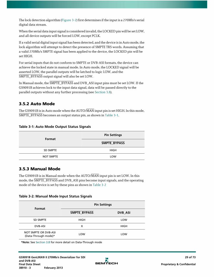
The GS9091B is in Auto mode when the AUTO/MAN input pin is set HIGH. In this mode, SMPTE_BYPASS becomes an output status pin, as shown in Table 3-1.
3.5.3 Manual Mode
The GS9091B is in Manual mode when the AUTO/MAN input pin is set LOW. In this mode, the SMPTE_BYPASS and DVB_ASI pins become input signals, and the operating mode of the device is set by these pins as shown in Table 3-2
.
Table 3-1: Auto Mode Output Status Signals
FormatPin Settings
SMPTE_BYPASS
SD SMPTE HIGH
NOT SMPTE LOW
Table 3-2: Manual Mode Input Status Signals
FormatPin Settings
SMPTE_BYPASS DVB_ASI
SD SMPTE HIGH LOW
DVB-ASI X HIGH
NOT SMPTE OR DVB-ASI (Data-Through mode)*
LOW LOW
*Note: See Section 3.8 for more detail on Data-Through mode
GS9091B GenLINX® II 270Mb/s Deserializer for SDI and DVB-ASIFinal Data Sheet 38910 - 3 February 2013
29 of 73
Proprietary & Confidential

3.6 SMPTE FunctionalityThe GS9091B is in SMPTE mode once the device has detected two SMPTE TRS sync words. The GS9091B will remain in SMPTE mode until six SMPTE TRS sync words fail to be detected.
TRS word detection is a continuous process, and the device will identify both 8-bit and 10-bit TRS words.
In Auto mode, the GS9091B sets the SMPTE_BYPASS pin HIGH to indicate that it has locked to a SMPTE input data stream. When operating in Manual mode, the DVB_ASI pin must be set LOW and the SMPTE_BYPASS pin must be set HIGH in order to enable SMPTE operation.
3.6.1 SMPTE Descrambling and Word Alignment
The GS9091B performs NRZI-to-NRZ decoding, descrambling according to SMPTE 259M-C, and word alignment of the data to the TRS sync words when in SMPTE mode.
Note: When 8-bit data is embedded into the SMPTE signal, the source must have the two LSBs of the 10-bit stream set to logic LOW in order for word alignment to function correctly.
3.6.2 Internal Flywheel
The GS9091B has an internal flywheel for the generation of internal / external timing signals, the detection and correction of certain error conditions, and the automatic detection of video standards. The flywheel is only operational in SMPTE mode.
The flywheel 'learns' the video standard by timing the horizontal and vertical reference information contained in the TRS ID words of the received video stream. The flywheel maintains information about the total line length, active line length, total number of lines per field / frame, and total active lines per field / frame for the received video stream. Full synchronization of the flywheel to the received video standard therefore requires one complete video frame.
Once synchronization has been achieved, the flywheel will continue to monitor the received TRS timing information to maintain synchronization.
The FW_EN input pin controls the synchronization mechanism of the flywheel. When this input signal is LOW, the flywheel will re-synchronize all pixel and line based counters on every received TRS ID word.
When FW_EN is set to logic HIGH, re-synchronization occurs when the flywheel detects three to four consecutive video lines containing mistimed TRS information. This provides a measure of noise immunity to internal and external timing signal generation.
The flywheel will be disabled if the device loses lock, or a LOW-to-HIGH transition occurs on the RESET pin.
GS9091B GenLINX® II 270Mb/s Deserializer for SDI and DVB-ASIFinal Data Sheet 38910 - 3 February 2013
30 of 73
Proprietary & Confidential
3.6.3 Switch Line Lock Handling
The principle of switch line lock handling is that the switching of synchronous video sources will only disturb the horizontal timing and alignment of the stream, whereas the vertical timing remains in synchronization.
3.6.3.1 Automatic Switch Line Lock Handling
The GS9091B also implements automatic switch line lock handling. By utilizing both the synchronous switch point defined in SMPTE RP168, and the automatic video standards detect function, the device automatically re-synchronizes the flywheel at the switch point. This will occur whether or not the device has detected TRS word errors. Word alignment re-synchronization will also take place at this time.
Automatic switch line lock handling will occur regardless of the setting of the FW_EN pin.
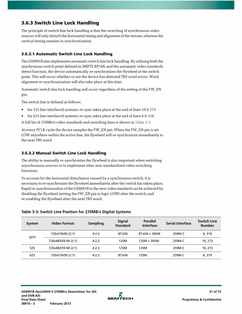
The switch line is defined as follows:
• for 525 line interlaced systems: re-sync takes place at the end of lines 10 & 273
• for 625 line interlaced systems: re-sync takes place at the end of lines 6 & 319
A full list of 270Mb/s video standards and switching lines is shown in Table 3-3.
At every PCLK cycle the device samples the FW_EN pin. When the FW_EN pin is set LOW anywhere within the active line, the flywheel will re-synchronize immediately to the next TRS word.
3.6.3.2 Manual Switch Line Lock Handling
The ability to manually re-synchronize the flywheel is also important when switching asynchronous sources or to implement other non-standardized video switching functions.
To account for the horizontal disturbance caused by a synchronous switch, it is necessary to re-synchronize the flywheel immediately after the switch has taken place. Rapid re-synchronization of the GS9091B to the new video standard can be achieved by disabling the flywheel (setting the FW_EN pin to logic LOW) after the switch, and re-enabling the flywheel after the next TRS word.
Table 3-3: Switch Line Position for 270MB/s Digital Systems
System Video Format SamplingSignal
StandardParallel
InterfaceSerial Interface
Switch Line Number
SDTI720x576/50 (2:1) 4:2:2 BT.656 BT.656 + 305M 259M-C 6, 319
720x483/59.94 (2:1) 4:2:2 125M 125M + 305M 259M-C 10, 273
525 720x483/59.94 (2:1) 4:2:2 125M 125M 259M-C 10, 273
625 720x576/50 (2:1) 4:2:2 BT.656 125M 259M-C 6, 319
GS9091B GenLINX® II 270Mb/s Deserializer for SDI and DVB-ASIFinal Data Sheet 38910 - 3 February 2013
31 of 73
Proprietary & Confidential

3.6.4 HVF Timing Signal Generation
The GS9091B extracts timing parameters, and outputs them to the F, V and H pins, from either the received TRS signals (FW_EN = LOW) or from the internal flywheel-timing generator (FW_EN = HIGH).
Horizontal blanking period (H), vertical blanking period (V), and field odd / even timing (F) are extracted and are available for output on any of the multi-function output port pins, if so programmed (see Section 3.12).
The H signal timing is configurable via the H_CONFIG bit of the internal IOPROC_DISABLE register as either active line-based blanking, or TRS-based blanking (see Table 3-14 in Section 3.9.8).
Active line-based blanking is enabled when the H_CONFIG bit is set LOW. In this mode, the H output is HIGH for the entire horizontal blanking period, including the EAV and SAV TRS words. This is the default H timing used by the device.
When H_CONFIG is set HIGH, TRS based blanking is enabled. In this case, the H output will be HIGH for the entire horizontal blanking period as indicated by the H bit in the received TRS ID words.
The timing of these signals is shown in Figure 3-3.
Note 1: When the internal FIFO is configured for video mode, the H, V, and F signals will be timed to the data output from the FIFO (see Section 3.10.1).
Note 2: When the GS9091B is configured for Low-latency mode, the H, V, and F output timing will be TRS-based as shown in Section 3.13. Active line-based timing is not available in this mode, and the setting of the H_CONFIG host interface bit will be ignored.
Figure 3-3: H,V,F Timing
Y/Cr/Cb DATA OUT
PCLK
H
V
F
XYZ(eav)0000003FF XYZ
(sav)0000003FF
H SIGNAL TIMING:
H_CONFIG = LOW
H_CONFIG = HIGH
GS9091B GenLINX® II 270Mb/s Deserializer for SDI and DVB-ASIFinal Data Sheet 38910 - 3 February 2013
32 of 73
Proprietary & Confidential

3.7 DVB-ASI FunctionalityDVB_ASI functionality is only supported in Manual mode.
In Manual mode, the DVB_ASI pin must be set to logic HIGH in order to enable DVB-ASI operation. The SMPTE_BYPASS pin will be ignored.
When using DVB-ASI mode, the use of application circuit in Figure 3-4 on page 33 is suggested. The use of this application circuit will prevent the internal PLL from false locking to a DVB-ASI signal harmonic rather than the 270MHz fundamental. This application circuit will detect the false lock state and restart the on-chip PLL. The application circuit does this by detecting if the LOCK has been de-asserted for longer than ~700μs, and if so resets the PLL by discharging the loop filter capacitor through a CMOS switch.
The applications circuit below show how this can be implemented by using a STG719 switch as a reference. Other low leakage CMOS switches may also be substituted within the circuit.
Figure 3-4: GS9091B False Lock Restart Circuit
The circuit above can be implemented using either a small state machine in an FPGA or general purpose I/O on a microcontroller in combination with some firmware. Typically, a system using the GS9091B will have an existing FPGA and/or microcontroller that may have some spare I/O that can be used to implement the false lock restart circuit. The choice of method will depend on what spare system resources are available. In either case, the waveform shown in Figure 3-5 on page 33 represents how the PLL restart must be driven. The delay values of 700μs and 20μs are nominal but the values can be longer. In the case where the SDI inputs are not driven with a valid DVB-ASI signal, the RESTART_PLL signal should be repeated indefinitely as long as LOCKED remains de-asserted.
Figure 3-5: GS9091B False Lock Restart Circuit Waveforms of False Lock After Power-up and False Lock After a Signal Switch.
FPGA or Microcontroller
GPIO
GS9090BGS9091B
LOCKED
INOUT
LF+
LF-
D
S1
In S21 6
2 5
3 4STG719
5
61
STG719
RESTART_PLL
DDI
POWER_OK
LOCKED
RES TART_PL L
~700µs~20µs
~700µs~20µs
VALID DVB-ASI INPUT SIGNAL VALID DVB-ASI INPUT SIGNAL
GS9091B GenLINX® II 270Mb/s Deserializer for SDI and DVB-ASIFinal Data Sheet 38910 - 3 February 2013
33 of 73
Proprietary & Confidential

3.7.1 DVB-ASI 8b/10b Decoding
The GS9091B will word align the data to the K28.5 sync characters, and 8b/10b decode and bit-swap the data to achieve bit alignment with the data outputs.
Note: DVB-ASI sync words must be immediately followed by an MPEG packet header for word alignment to correctly function.
The extracted 8-bit data will be presented to DOUT [7:0], bypassing all internal SMPTE mode data processing.
3.7.2 Status Signal Outputs
In DVB-ASI mode, the DOUT9 and DOUT8 pins will be configured as DVB-ASI status signals WORDERR and SYNCOUT respectively.
SYNCOUT will be HIGH whenever a K28.5 sync character is present on the output. WORDERR will be HIGH whenever the device has detected an illegal 8b/10b code word or there is a running disparity error.
3.8 Data-Through FunctionalityThe GS9091B may be configured to operate as a simple serial-to-parallel converter. In this mode, the data is output to the parallel output without performing any decoding, descrambling, or word-alignment.
Data-Through functionality is enabled when the AUTO/MAN, SMPTE_BYPASS, and DVB_ASI input pins are set to logic LOW. Under these conditions, the GS9091B allows 270Mb/s input data not conforming to SMPTE or DVB-ASI streams to be reclocked and deserialized. If the device is in Data-Through mode, and the reclocker locks to the data stream, the LOCKED pin will be representative of the serial digital input data frequency.
GS9091B GenLINX® II 270Mb/s Deserializer for SDI and DVB-ASIFinal Data Sheet 38910 - 3 February 2013
34 of 73
Proprietary & Confidential
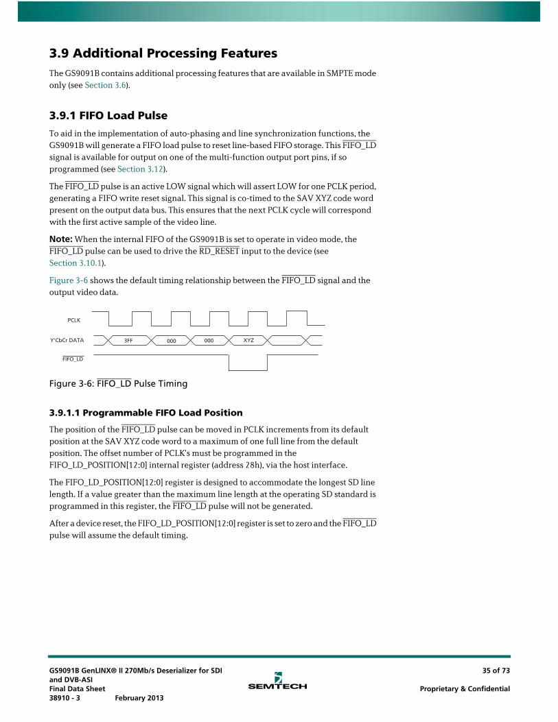
3.9 Additional Processing FeaturesThe GS9091B contains additional processing features that are available in SMPTE mode only (see Section 3.6).
3.9.1 FIFO Load Pulse
To aid in the implementation of auto-phasing and line synchronization functions, the GS9091B will generate a FIFO load pulse to reset line-based FIFO storage. This FIFO_LD signal is available for output on one of the multi-function output port pins, if so programmed (see Section 3.12).
The FIFO_LD pulse is an active LOW signal which will assert LOW for one PCLK period, generating a FIFO write reset signal. This signal is co-timed to the SAV XYZ code word present on the output data bus. This ensures that the next PCLK cycle will correspond with the first active sample of the video line.
Note: When the internal FIFO of the GS9091B is set to operate in video mode, the FIFO_LD pulse can be used to drive the RD_RESET input to the device (see Section 3.10.1).
Figure 3-6 shows the default timing relationship between the FIFO_LD signal and the output video data.
Figure 3-6: FIFO_LD Pulse Timing
3.9.1.1 Programmable FIFO Load Position
The position of the FIFO_LD pulse can be moved in PCLK increments from its default position at the SAV XYZ code word to a maximum of one full line from the default position. The offset number of PCLK's must be programmed in the FIFO_LD_POSITION[12:0] internal register (address 28h), via the host interface.
The FIFO_LD_POSITION[12:0] register is designed to accommodate the longest SD line length. If a value greater than the maximum line length at the operating SD standard is programmed in this register, the FIFO_LD pulse will not be generated.
After a device reset, the FIFO_LD_POSITION[12:0] register is set to zero and the FIFO_LD pulse will assume the default timing.
0003FF 000 XYZY'CbCr DATA
PCLK
FIFO_LD
GS9091B GenLINX® II 270Mb/s Deserializer for SDI and DVB-ASIFinal Data Sheet 38910 - 3 February 2013
35 of 73
Proprietary & Confidential
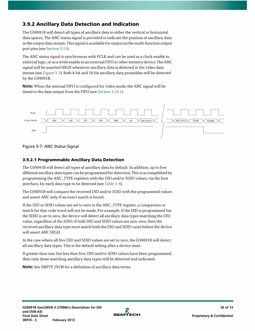
3.9.2 Ancillary Data Detection and Indication
The GS9091B will detect all types of ancillary data in either the vertical or horizontal data spaces. The ANC status signal is provided to indicate the position of ancillary data in the output data stream. This signal is available for output on the multi-function output port pins (see Section 3.12).
The ANC status signal is synchronous with PCLK and can be used as a clock enable to external logic, or as a write enable to an external FIFO or other memory device. The ANC signal will be asserted HIGH whenever ancillary data is detected in the video data stream (see Figure 3-7). Both 8-bit and 10-bit ancillary data preambles will be detected by the GS9091B.
Note: When the internal FIFO is configured for video mode, the ANC signal will be timed to the data output from the FIFO (see Section 3.10.1).
Figure 3-7: ANC Status Signal
3.9.2.1 Programmable Ancillary Data Detection
The GS9091B will detect all types of ancillary data by default. In addition, up to five different ancillary data types can be programmed for detection. This is accomplished by programming the ANC_TYPE registers with the DID and/or SDID values, via the host interface, for each data type to be detected (see Table 3-4).
The GS9091B will compare the received DID and/or SDID with the programmed values and assert ANC only if an exact match is found.
If the DID or SDID values are set to zero in the ANC_TYPE register, a comparison or match for that code word will not be made. For example, if the DID is programmed but the SDID is set to zero, the device will detect all ancillary data types matching the DID value, regardless of the SDID. If both DID and SDID values are non-zero, then the received ancillary data type must match both the DID and SDID cases before the device will assert ANC HIGH.
In the case where all five DID and SDID values are set to zero, the GS9091B will detect all ancillary data types. This is the default setting after a device reset.
If greater than one, but less than five, DID and/or SDID values have been programmed, then only those matching ancillary data types will be detected and indicated.
Note: See SMPTE 291M for a definition of ancillary data terms.
3FF000 3FF DID DBN ANC DATA CSUM BLANK
ANC
Y'CbCr DATA
PCLK
DC ANC DATA
GS9091B GenLINX® II 270Mb/s Deserializer for SDI and DVB-ASIFinal Data Sheet 38910 - 3 February 2013
36 of 73
Proprietary & Confidential

3.9.3 EDH Packet Detection
The GS9091B will determine if EDH packets are present in the incoming video data and assert the EDH_DETECT output status signal appropriately.
EDH_DETECT will be set HIGH when EDH packets have been detected and will remain HIGH until EDH packets are no longer present. The signal will be set LOW at the end of the vertical blanking (falling edge of V) if an EDH packet has not been received and detected during vertical blanking.
EDH_DETECT can be programmed to be available for output on the multi-function output port pins (see Section 3.12). The EDH_DETECT bit is also available in the DATA_FORMAT register at address 04h (see Table 3-7).
Table 3-4: Host Interface Description for Programmable Ancillary Data Type registers
Register Name Bit Name Description R/W Default
ANC_TYPE 1 Address: 0Ah
15-8 ANC_TYPE1[15:8]Used to program the DID for ancillary data detection at ANC output
R/W 0
7-0 ANC_TYPE1[7:0]
Used to program the SDID for ancillary data detection at ANC output. Should be set to zero if no SDID is present in the ancillary data packet to be detected.
R/W 0
ANC_TYPE 2 Address: 0Bh
15-8 ANC_TYPE2[15:8]Used to program the DID for ancillary data detection at ANC output
R/W 0
7-0 ANC_TYPE2[7:0]
Used to program the SDID for ancillary data detection at ANC output. Should be set to zero if no SDID is present in the ancillary data packet to be detected.
R/W 0
ANC_TYPE 3 Address: 0Ch
15-8 ANC_TYPE3[15:8]Used to program the DID for ancillary data detection at ANC output
R/W 0
7-0 ANC_TYPE3[7:0]
Used to program the SDID for ancillary data detection at ANC output. Should be set to zero if no SDID is present in the ancillary data packet to be detected.
R/W 0
ANC_TYPE 4 Address: 0Dh
15-8 ANC_TYPE4[15:8]Used to program the DID for ancillary data detection at ANC output
R/W 0
7-0 ANC_TYPE4[7:0]
Used to program the SDID for ancillary data detection at ANC output. Should be set to zero if no SDID is present in the ancillary data packet to be detected.
R/W 0
ANC_TYPE 5 Address: 0Eh
15-8 ANC_TYPE5[15:8]Used to program the DID for ancillary data detection at ANC output
R/W 0
7-0 ANC_TYPE5[7:0]
Used to program the SDID for ancillary data detection at ANC output. Should be set to zero if no SDID is present in the ancillary data packet to be detected.
R/W 0
GS9091B GenLINX® II 270Mb/s Deserializer for SDI and DVB-ASIFinal Data Sheet 38910 - 3 February 2013
37 of 73
Proprietary & Confidential
3.9.4 EDH Flag Detection
As described in Section 3.9.3, the GS9091B can detect EDH packets in the received data stream. The EDH flags for ancillary data, active picture, and full field areas are extracted from the detected EDH packets and placed in the EDH_FLAG_IN register at address 02h (Table 3-5).
When the EDH_FLAG_UPDATE bit in the DATA_FORMAT register 04h (Table 3-7) is set HIGH, the GS9091B will update the ancillary data, full field, and active picture EDH flags according to SMPTE RP165. The updated EDH flags are available in the EDH_FLAG_OUT register at address 03h (Table 3-6). The EDH packet output from the device will contain the updated flags.
One set of flags is provided for both fields 1 and 2. Field 1 flag data will be overwritten by field 2 flag data.
When EDH packets are not detected, the UES flags in the EDH_FLAG_OUT register will be set HIGH to signify that the received signal does not support Error Detection and Handling. In addition, the EDH_DETECT bit will be set LOW. These flags are set regardless of the setting of the EDH_FLAG_UPDATE bit.
EDH_FLAG_OUT and EDH_FLAG_UPDATE may be read by the host interface at any time during the received frame except on the lines defined in SMPTE RP165, where these flags are updated.
The GS9091B will indicate the CRC validity for both active picture and full field CRCs. The AP_CRC_V bit in the DATA_FORMAT register indicates the active picture CRC validity, and the FF_CRC_V bit indicates the full field CRC validity (see Table 3-7). When EDH_DETECT = LOW, these bits will be cleared.
The EDH_FLAG_OUT and EDH_FLAG_UPDATE register values remain set until overwritten by the decoded flags in the next received EDH packet in the following field. When an EDH packet is not detected during vertical blanking, the flag registers will be cleared at the end of the vertical blanking period.
GS9091B GenLINX® II 270Mb/s Deserializer for SDI and DVB-ASIFinal Data Sheet 38910 - 3 February 2013
38 of 73
Proprietary & Confidential

Table 3-5: Host Interface Description for EDH Flag Registers
Register Name Bit Name Description R/W Default
EDH_FLAG_IN
Address: 02h
15 – Not Used – –
14 ANC-UES_IN Ancillary Unknown Error Status Flag R 0
13 ANC-IDA_IN Ancillary Internal device error Detected Already Flag. R 0
12 ANC-IDH_IN Ancillary Internal device error Detected Here Flag. R 0
11 ANC-EDA_IN Ancillary Error Detected Already Flag. R 0
10 ANC-EDH_IN Ancillary Error Detected Here Flag. R 0
9 FF-UES_IN Full Field Unknown Error Status Flag. R 0
8 FF-IDA_IN Full Field Internal device error Detected Already Flag. R 0
7 FF-IDH_IN Full Field Internal device error Detected Here Flag. R 0
6 FF-EDA_IN Full Field Error Detected Already Flag. R 0
5 FF-EDH_IN Full Field Error Detected Here Flag. R 0
4 AP-UES_IN Active Picture Unknown Error Status Flag. R 0
3 AP-IDA_INActive Picture Internal device error Detected Already Flag.
R 0
2 AP-IDH_INActive Picture Internal device error Detected Here Flag
R 0
1 AP-EDA_IN Active Picture Error Detected Already Flag. R 0
0 AP-EDH_IN Active Picture Error Detected Here Flag. R 0
GS9091B GenLINX® II 270Mb/s Deserializer for SDI and DVB-ASIFinal Data Sheet 38910 - 3 February 2013
39 of 73
Proprietary & Confidential
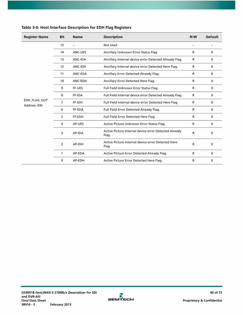
Table 3-6: Host Interface Description for EDH Flag Registers
Register Name Bit Name Description R/W Default
EDH_FLAG_OUT
Address: 03h
15 – Not Used – –
14 ANC-UES Ancillary Unknown Error Status Flag R 0
13 ANC-IDA Ancillary Internal device error Detected Already Flag. R 0
12 ANC-IDH Ancillary Internal device error Detected Here Flag. R 0
11 ANC-EDA Ancillary Error Detected Already Flag. R 0
10 ANC-EDH Ancillary Error Detected Here Flag. R 0
9 FF-UES Full Field Unknown Error Status Flag. R 0
8 FF-IDA Full Field Internal device error Detected Already Flag. R 0
7 FF-IDH Full Field Internal device error Detected Here Flag. R 0
6 FF-EDA Full Field Error Detected Already Flag. R 0
5 FF-EDH Full Field Error Detected Here Flag. R 0
4 AP-UES Active Picture Unknown Error Status Flag. R 0
3 AP-IDAActive Picture Internal device error Detected Already Flag.
R 0
2 AP-IDHActive Picture Internal device error Detected Here Flag
R 0
1 AP-EDA Active Picture Error Detected Already Flag. R 0
0 AP-EDH Active Picture Error Detected Here Flag. R 0
GS9091B GenLINX® II 270Mb/s Deserializer for SDI and DVB-ASIFinal Data Sheet 38910 - 3 February 2013
40 of 73
Proprietary & Confidential

3.9.5 SMPTE 352M Payload Identifier
The GS9091B can receive and detect the presence of the SMPTE 352M payload identifier.
Upon detection of this packet, the device will extract the four words contained in the packet to the VIDEO_FORMAT_OUT_A and VIDEO_FORMAT_OUT_B registers at addresses 10h and 0fh (Table 3-8). The device will also indicate the version of the payload packet in bit 7 of the DATA_FORMAT register (Table 3-7). When bit 7 is set HIGH the received SMPTE 352M packet is version 1, otherwise it is version 0.
The VIDEO_FORMAT registers will only be updated if the received checksum is the same as the locally calculated checksum.
If the device loses lock to the input data stream (LOCKED = LOW), or if the SMPTE_BYPASS pin is asserted LOW, the VIDEO_FORMAT_OUT_A and VIDEO_FORMAT_OUT_B registers will be cleared to zero, indicating an undefined format. This is also the default setting after a device reset.
Table 3-7: Host Interface Description for Data Format Register
Register Name
Bit Name Description R/W Default
DATA_FORMAT
Address: 04h
15-12 – Not Used – –
11 EDH_FLAG_UPDATEWhen set HIGH by the application layer, the device will update the ancillary data, full field, and active picture EDH flags according to SMPTE RP165.
R/W 0
10 AP_CRC_V Active Picture CRC Valid bit. R 0
9 FF_CRC_V Full Field CRC Valid bit. R 0
8 EDH_DETECTSet HIGH by the device when EDH packets are detected in the incoming video data.
R 0
7 VERSION_352MIndicates whether decoded SMPTE 352M packet is version 0 or version 1. See Section 3.9.5.
R 0
6-5 – Not Used – –
4 STD_LOCKStandard Lock bit. This bit will be set HIGH when the flywheel has achieved full synchronization to the received video standard. See Section 3.9.6.
R 0
3-0 DATA_FORMAT[3:0]Displays the data format being carried on the serial digital interface. See Section 3.9.6.1.
R 0
GS9091B GenLINX® II 270Mb/s Deserializer for SDI and DVB-ASIFinal Data Sheet 38910 - 3 February 2013
41 of 73
Proprietary & Confidential

3.9.6 Automatic Video Standard and Data Format Detection
The GS9091B can detect the input video standard and data format by using the timing parameters extracted from the received TRS ID. Total samples per line, active samples per line, total lines per frame, and active lines per field are all calculated and presented to the host interface via the RASTER_STRUCTURE registers (Table 3-9).
Also associated with the RASTER_STRUCTURE registers is the STD_LOCK status bit. The GS9091B will set STD_LOCK HIGH when the flywheel has achieved full synchronization to the received video standard. STD_LOCK is stored in the DATA_FORMAT register (Table 3-7).
The four RASTER_STRUCTURE registers, as well as the STD_LOCK status bit will default to zero after a device reset, or if the device loses lock to the input data stream (LOCKED = LOW).
Table 3-8: Host Interface Description for SMPTE 352M Payload Identifier Registers
Register Name Bit Name Description R/W Default
VIDEO_FORMAT_OUT_B Address: 10h
15-8 SMPTE 352M Byte 4Data will be available in this register when Video Payload Identification Packets are detected in the data stream.
R 0
7-0 SMPTE 352M Byte 3Data will be available in this register when Video Payload Identification Packets are detected in the data stream.
R 0
VIDEO_FORMAT_OUT_A Address: 0Fh
15-8 SMPTE 352M Byte 2Data will be available in this register when Video Payload Identification Packets are detected in the data stream.
R 0
7-0 SMPTE 352M Byte 1Data will be available in this register when Video Payload Identification Packets are detected in the data stream.
R 0
Table 3-9: Host Interface Description for Raster Structure Registers
Register Name Bit Name Description R/W Default
RASTER_STRUCTURE1 Address: 11h
15-11 – Not Used – –
10-0 RASTER_STRUCTURE1[10:0] Total Lines Per Frame R 0
RASTER_STRUCTURE2 Address: 12h
15-13 – Not Used – –
12-0 RASTER_STRUCTURE2[12:0] Total Words Per Line R 0
RASTER_STRUCTURE3 Address: 13h
15-13 – Not Used – –
12-0 RASTER_STRUCTURE3[12:0] Words Per Active Line R 0
RASTER_STRUCTURE4 Address: 14h
15-11 – Not Used – –
10-0 RASTER_STRUCTURE4[10:0] Active Lines Per Field R 0
GS9091B GenLINX® II 270Mb/s Deserializer for SDI and DVB-ASIFinal Data Sheet 38910 - 3 February 2013
42 of 73
Proprietary & Confidential
3.9.6.1 Data Format Indication
The GS9091B can extract the data format being carried on the serial digital interface (i.e. SDTI, SDI, or DVB-ASI). This information is represented by bits 0 to 3 of the DATA_FORMAT register (Table 3-7).
DATA_FORMAT[3:0] register codes are shown in Table 3-10.
The DATA_FORMAT[3:0] register defaults to Fh (undefined) after a system reset. The register will also be set to its default value if the device is not locked (LOCKED = LOW), or if both SMPTE_BYPASS and DVB_ASI pins are LOW.
3.9.7 Error Detection and Indication
The GS9091B contains a number of error detection functions to enhance operation of the device when operating in SMPTE mode. These functions, except lock error detection, will not be available in DVB-ASI mode (Section 3.7) or Data-Through mode (Section 3.8).
The ERROR_STATUS register is at address 01h (Table 3-11). All bits, except the LOCK_ERR bit, will be cleared at the start of each video field or when read by the host interface, whichever condition occurs first.
All bits, with the exception of the LOCK_ERR, will also be cleared if a change in the video standard is detected, if the device loses lock to the input data stream (LOCKED = LOW), or if the SMPTE_BYPASS pin is asserted LOW.
The ERROR_STATUS register, including the LOCK_ERR bit, will be set LOW during a system reset (RESET = LOW).
Table 3-10: Data Format Register Codes
Data Format[3:0] Data Format Applicable Standards
0h SDTI DVCPRO - No ECC SMPTE 321M
1h SDTI DVCPRO - ECC SMPTE 321M
2h SDTI DVCAM SMPTE 322M
3h SDTI CP SMPTE 326M
4h Other SDTI fixed block size –
5h Other SDTI variable block size –
6h SDI –
7h DVB-ASI –
8h ~ Eh Reserved –
Fh Unknown data format –
GS9091B GenLINX® II 270Mb/s Deserializer for SDI and DVB-ASIFinal Data Sheet 38910 - 3 February 2013
43 of 73
Proprietary & Confidential

The ERROR_MASK register (Table 3-12) is available to individually mask each error type in the ERROR_STATUS register. Each error type may be individually masked by setting its corresponding bit HIGH. The bits of the ERROR_MASK register will default to '0' after a device reset, thus allowing all error types to be detected.
The DATA_ERROR signal pin indicates the status of the ERROR_STATUS register. This output pin is an inverted logical OR of each error status flag stored in the ERROR_STATUS register. DATA_ERROR will be set LOW by the device when an error condition that has not been masked is detected.
Table 3-11: Host Interface Description for Error Status Register
Register Name Bit Name Description R/W Default
ERROR_STATUS
Address: 01h
15-7 – Not Used – –
6 VD_STD_ERR
Video Standard Error Flag. Set HIGH when a mismatch between the received SMPTE 352M packets (version 1 or version 0) and the calculated video standard occurs.
R 0
5 FF_CRC_ERRFull Field CRC Error Flag. Set HIGH when a Full Field (FF) CRC mismatch has been detected in Field 1 or 2
R 0
4 AP_CRC_ERRActive Picture CRC Error Flag. Set HIGH when an Active Picture (AP) CRC mismatch has been detected in Field 1 or 2.
R 0
3 LOCK_ERRLock Error Flag. Set HIGH whenever the LOCKED pin is LOW (indicating the device is not correctly locked).
R 0
2 CS_ERRChecksum Error Flag. Set HIGH when ancillary data packet checksum error has been detected.
R 0
1 SAV_ERRStart of Active Video Error Flag. Set HIGH when TRS errors are detected in either 8-bit or 10-bit TRS words.
R 0
0 EAV_ERREnd of Active Video Error Flag. Set HIGH when TRS errors are detected in either 8-bit or 10-bit TRS words.
R 0
GS9091B GenLINX® II 270Mb/s Deserializer for SDI and DVB-ASIFinal Data Sheet 38910 - 3 February 2013
44 of 73
Proprietary & Confidential
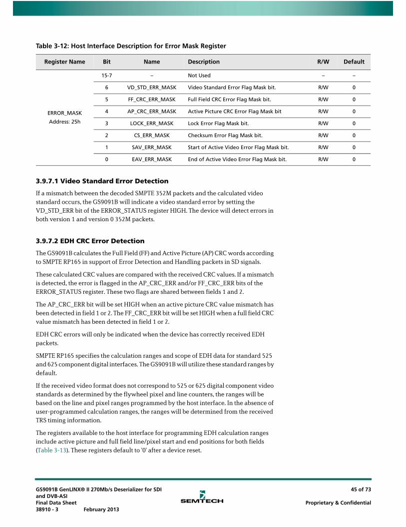
3.9.7.1 Video Standard Error Detection
If a mismatch between the decoded SMPTE 352M packets and the calculated video standard occurs, the GS9091B will indicate a video standard error by setting the VD_STD_ERR bit of the ERROR_STATUS register HIGH. The device will detect errors in both version 1 and version 0 352M packets.
3.9.7.2 EDH CRC Error Detection
The GS9091B calculates the Full Field (FF) and Active Picture (AP) CRC words according to SMPTE RP165 in support of Error Detection and Handling packets in SD signals.
These calculated CRC values are compared with the received CRC values. If a mismatch is detected, the error is flagged in the AP_CRC_ERR and/or FF_CRC_ERR bits of the ERROR_STATUS register. These two flags are shared between fields 1 and 2.
The AP_CRC_ERR bit will be set HIGH when an active picture CRC value mismatch has been detected in field 1 or 2. The FF_CRC_ERR bit will be set HIGH when a full field CRC value mismatch has been detected in field 1 or 2.
EDH CRC errors will only be indicated when the device has correctly received EDH packets.
SMPTE RP165 specifies the calculation ranges and scope of EDH data for standard 525 and 625 component digital interfaces. The GS9091B will utilize these standard ranges by default.
If the received video format does not correspond to 525 or 625 digital component video standards as determined by the flywheel pixel and line counters, the ranges will be based on the line and pixel ranges programmed by the host interface. In the absence of user-programmed calculation ranges, the ranges will be determined from the received TRS timing information.
The registers available to the host interface for programming EDH calculation ranges include active picture and full field line/pixel start and end positions for both fields (Table 3-13). These registers default to '0' after a device reset.
Table 3-12: Host Interface Description for Error Mask Register
Register Name Bit Name Description R/W Default
ERROR_MASK
Address: 25h
15-7 – Not Used – –
6 VD_STD_ERR_MASK Video Standard Error Flag Mask bit. R/W 0
5 FF_CRC_ERR_MASK Full Field CRC Error Flag Mask bit. R/W 0
4 AP_CRC_ERR_MASK Active Picture CRC Error Flag Mask bit R/W 0
3 LOCK_ERR_MASK Lock Error Flag Mask bit. R/W 0
2 CS_ERR_MASK Checksum Error Flag Mask bit. R/W 0
1 SAV_ERR_MASK Start of Active Video Error Flag Mask bit. R/W 0
0 EAV_ERR_MASK End of Active Video Error Flag Mask bit. R/W 0
GS9091B GenLINX® II 270Mb/s Deserializer for SDI and DVB-ASIFinal Data Sheet 38910 - 3 February 2013
45 of 73
Proprietary & Confidential

If any or all of these register values are zero, then the EDH CRC calculation ranges will be determined from the flywheel generated timing. The first active and full field pixel will always be the first pixel after the SAV TRS code word. The last active and full field pixel will always be the last pixel before the start of the EAV TRS code words.
Table 3-13: Host Interface Description for EDH Calculation Range Registers
Register Name Bit Name Description R/W Default
AP_LINE_START_F0 Address: 15h
15-11 – Not Used – –
10-0 AP_LINE_START_F0[10:0]Field 0 Active Picture start line data used to set EDH calculation range outside of SMPTE RP 165 values.
R/W 0
AP_LINE_END_F0 Address: 16h
15-11 – Not Used – –
10-0 AP_LINE_END_F0[10:0]Field 0 Active Picture end line data used to set EDH calculation range outside of SMPTE RP 165 values.
R/W 0
AP_LINE_START_F1 Address: 17h
15-11 – Not Used – –
10-0 AP_LINE_START_F1[10:0]Field 1 Active Picture start line data used to set EDH calculation range outside of SMPTE RP 165 values.
R/W 0
AP_LINE_END_F1 Address: 18h
15-11 – Not Used – –
10-0 AP_LINE_END_F1[10:0]Field 1 Active Picture end line data used to set EDH calculation range outside of SMPTE RP 165 values.
R/W 0
FF_LINE_START_F0 Address: 19h
15-11 – Not Used – –
10-0 FF_LINE_START_F0[10:0]Field 0 Full Field start line data used to set EDH calculation range outside of SMPTE RP 165 values.
R/W 0
FF_LINE_END_F0 Address: 1Ah
15-11 – Not Used – –
10-0 FF_LINE_END_F0[10:0]Field 0 Full Field end line data used to set EDH calculation range outside of SMPTE RP 165 values.
R/W 0
FF_LINE_START_F1 Address: 1Bh
15-11 – Not Used – –
10-0 FF_LINE_START_F1[10:0]Field 1 Full Field start line data used to set EDH calculation range outside of SMPTE RP 165 values.
R/W 0
FF_LINE_END_F1 Address: 1Ch
15-11 – Not Used – –
10-0 FF_LINE_END_F1[10:0]Field 1 Full Field end line data used to set EDH calculation range outside of SMPTE RP 165 values.
R/W 0
AP_PIXEL_START_F0 Address: 1Dh
15-13 – Not Used – –
12-0 AP_PIXEL_START_F0[12:0]Field 0 Active Picture start pixel data used to set EDH calculation range outside of SMPTE RP 165 values.
R/W 0
GS9091B GenLINX® II 270Mb/s Deserializer for SDI and DVB-ASIFinal Data Sheet 38910 - 3 February 2013
46 of 73
Proprietary & Confidential
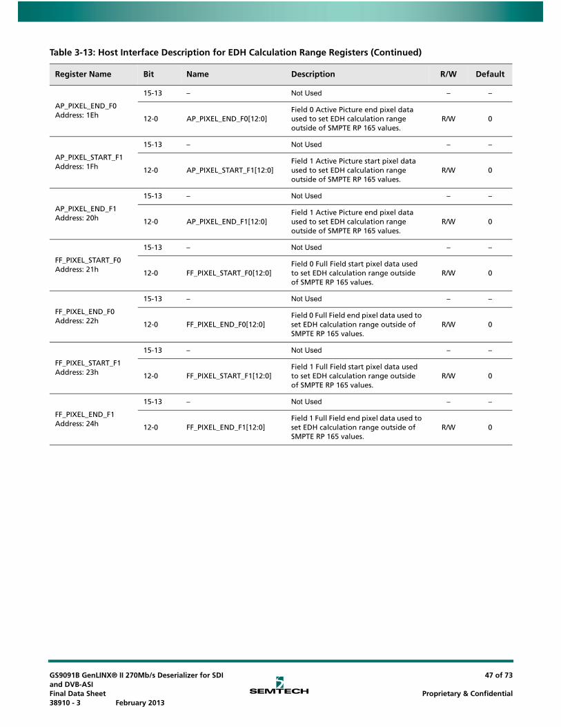
AP_PIXEL_END_F0 Address: 1Eh
15-13 – Not Used – –
12-0 AP_PIXEL_END_F0[12:0]Field 0 Active Picture end pixel data used to set EDH calculation range outside of SMPTE RP 165 values.
R/W 0
AP_PIXEL_START_F1 Address: 1Fh
15-13 – Not Used – –
12-0 AP_PIXEL_START_F1[12:0]Field 1 Active Picture start pixel data used to set EDH calculation range outside of SMPTE RP 165 values.
R/W 0
AP_PIXEL_END_F1 Address: 20h
15-13 – Not Used – –
12-0 AP_PIXEL_END_F1[12:0]Field 1 Active Picture end pixel data used to set EDH calculation range outside of SMPTE RP 165 values.
R/W 0
FF_PIXEL_START_F0 Address: 21h
15-13 – Not Used – –
12-0 FF_PIXEL_START_F0[12:0]Field 0 Full Field start pixel data used to set EDH calculation range outside of SMPTE RP 165 values.
R/W 0
FF_PIXEL_END_F0 Address: 22h
15-13 – Not Used – –
12-0 FF_PIXEL_END_F0[12:0]Field 0 Full Field end pixel data used to set EDH calculation range outside of SMPTE RP 165 values.
R/W 0
FF_PIXEL_START_F1 Address: 23h
15-13 – Not Used – –
12-0 FF_PIXEL_START_F1[12:0]Field 1 Full Field start pixel data used to set EDH calculation range outside of SMPTE RP 165 values.
R/W 0
FF_PIXEL_END_F1 Address: 24h
15-13 – Not Used – –
12-0 FF_PIXEL_END_F1[12:0]Field 1 Full Field end pixel data used to set EDH calculation range outside of SMPTE RP 165 values.
R/W 0
Table 3-13: Host Interface Description for EDH Calculation Range Registers (Continued)
Register Name Bit Name Description R/W Default
GS9091B GenLINX® II 270Mb/s Deserializer for SDI and DVB-ASIFinal Data Sheet 38910 - 3 February 2013
47 of 73
Proprietary & Confidential
3.9.7.3 Lock Error Detection
The LOCKED pin of the GS9091B asserts HIGH when the device has correctly locked to the received data stream (see Section 3.5.1).
The GS9091B will also indicate lock error to the host interface when LOCKED = LOW by setting the LOCK_ERR bit in the ERROR_STATUS register HIGH (Table 3-11).
3.9.7.4 Ancillary Data Checksum Error Detection
The GS9091B will calculate checksums for all received ancillary data types and compare the calculated values to the received checksum words. If a mismatch is detected, the CS_ERR bit of the ERROR_STATUS register will be set HIGH (Table 3-11).
Although the GS9091B will calculate and compare checksum values for all ancillary data types by default, the host interface may be programmed to check only certain types of ancillary data checksums, as described in Section 3.9.2.1.
3.9.7.5 TRS Error Detection
TRS error flags are generated by the GS9091B when the received TRS H timing does not correspond to the internal flywheel timing, or when the received TRS Hamming codes are incorrect.
These errors are flagged via the SAV_ERR and/or EAV_ERR bits of the ERROR_STATUS register (Table 3-11). Both 8-bit and 10-bit SAV and EAV errors are handled by the GS9091B.
Note: H timing based TRS errors will only be detected if the FW_EN pin is set HIGH. F & V timing errors are not detected or corrected.
3.9.8 Additional SMPTE Mode Processing
The GS9091B contains an additional processing block which is available in SMPTE mode only. The IOPROC_EN pin must be set HIGH to enable these functions. These functions, which are all enabled by default, may be enabled or disabled individually by setting bits 0 to 3 in the IOPROC_DISABLE register (Table 3-14).
Note: After a device reset, these functions will revert to their default values.
GS9091B GenLINX® II 270Mb/s Deserializer for SDI and DVB-ASIFinal Data Sheet 38910 - 3 February 2013
48 of 73
Proprietary & Confidential

Table 3-14: Host Interface Description for Internal Processing Disable Register
Register Name Bit Name Description R/W Default
IOPROC_DISABLE
Address: 00h
15-10 – Not Used – –
9 ANC_PKT_EXT
Ancillary Packet Extraction. When the FIFO is configured for Ancillary Data Extraction mode, the application layer must set this bit HIGH to begin extraction.
NOTE: Setting ANC_PKT_EXT LOW will not automatically disable ancillary data extraction (see Section 3.10.3.1).
R/W 0
8-7 FIFO_MODE[1:0]FIFO Mode: These bits control which mode the internal FIFO is operating in (see Table 3-15)
R/W 0
6 H_CONFIG
Horizontal sync timing output configuration. Set LOW for active line blanking timing. Set HIGH for H blanking based on the H bit setting of the TRS word. See Figure 3-3 in Section 3.6.4.
R/W 0
5-4 Not Used.
3 ILLEGAL_REMAPIllegal Code re-mapping. Correction of illegal code words within the active picture. Set HIGH to disable. The IOPROC_EN pin must be set HIGH.
R/W 0
2 EDH_CRC_INS
Error Detection & Handling (EDH) Cyclical Redundancy Check (CRC) error correction insertion. Set HIGH to disable. The IOPROC_EN pin must be set HIGH.
R/W 0
1 ANC_CSUM_INSAncillary Data Checksum insertion. Set HIGH to disable. The IOPROC_EN pin must be set HIGH.
R/W 0
0 TRS_INS
Timing Reference Signal Insertion. The device will correct TRS based errors when set LOW (see Section 3.9.8.4). The IOPROC_EN pin must also be HIGH.
Set this bit HIGH to disable.
R/W 0
GS9091B GenLINX® II 270Mb/s Deserializer for SDI and DVB-ASIFinal Data Sheet 38910 - 3 February 2013
49 of 73
Proprietary & Confidential
3.9.8.1 Illegal Code Remapping
If the ILLEGAL_REMAP bit of the IOPROC_DISABLE register is set LOW, the GS9091B will remap all codes within the active picture between the values 3FCh and 3FFh to 3FBh. All codes within the active picture area between the values 00h and 03h will be re-mapped to 04h. In addition, 8-bit TRS and ancillary data preambles will be remapped to 10-bit values.
3.9.8.2 EDH CRC Error Correction
If the EDH_CRC_INS bit of the IOPROC_DISABLE register is set LOW, the GS9091B will calculate and overwrite the active picture and full field CRC words into the EDH data packets received by the device.
Additionally, when EDH_CRC_INS is LOW, the device will set the active picture and full field CRC ‘V’ bits HIGH in the EDH packet (see Section 3.9.4). The AP_CRC_V and FF_CRC_V register bits will only report the received EDH validity flags.
EDH CRC calculation ranges are described in Section 3.9.7.2.
Note: Although the GS9091B will modify and insert EDH CRC words and EDH packet checksums, the device will only update EDH error flags when the EDH_FLAG_UPDATE bit is set HIGH (see Section 3.9.4).
3.9.8.3 Ancillary Data Checksum Error Correction
If the ANC_CSUM_INS bit of the IOPROC_DISABLE register is set LOW, ancillary checksum error correction and insertion is enabled, and the GS9091B will calculate and overwrite ancillary data checksums for all ancillary data words by default. If the Ancillary Data type has been specified in the ANC_TYPE registers of the host interface (see Section 3.9.2.1), only the checksums for the ancillary data programmed will be updated.
3.9.8.4 TRS Error Correction
If the TRS_INS bit of the IOPROC_DISABLE register is set LOW, TRS error correction and insertion is enabled. In this mode, the GS9091B will calculate and overwrite 10-bit TRS code words as required.
TRS code word generation will be performed using the timing parameters generated by the flywheel to provide an element of noise immunity, and will only take place if the flywheel in enabled (FW_EN = HIGH).
Note: Only H timing based errors will be corrected (see Section 3.9.7.5).
GS9091B GenLINX® II 270Mb/s Deserializer for SDI and DVB-ASIFinal Data Sheet 38910 - 3 February 2013
50 of 73
Proprietary & Confidential
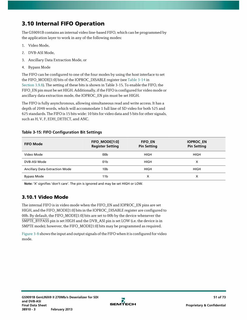
3.10 Internal FIFO OperationThe GS9091B contains an internal video line-based FIFO, which can be programmed by the application layer to work in any of the following modes:
1. Video Mode,
2. DVB-ASI Mode,
3. Ancillary Data Extraction Mode, or
4. Bypass Mode
The FIFO can be configured to one of the four modes by using the host interface to set the FIFO_MODE[1:0] bits of the IOPROC_DISABLE register (see Table 3-14 in Section 3.9.8). The setting of these bits is shown in Table 3-15. To enable the FIFO, the FIFO_EN pin must be set HIGH. Additionally, if the FIFO is configured for video mode or ancillary data extraction mode, the IOPROC_EN pin must be set HIGH.
The FIFO is fully asynchronous, allowing simultaneous read and write access. It has a depth of 2048 words, which will accommodate 1 full line of SD video for both 525 and 625 standards. The FIFO is 15 bits wide: 10 bits for video data and 5 bits for other signals, such as H, V, F, EDH_DETECT, and ANC.
3.10.1 Video Mode
The internal FIFO is in video mode when the FIFO_EN and IOPROC_EN pins are set HIGH, and the FIFO_MODE[1:0] bits in the IOPROC_DISABLE register are configured to 00b. By default, the FIFO_MODE[1:0] bits are set to 00b by the device whenever the SMPTE_BYPASS pin is set HIGH and the DVB_ASI pin is set LOW (i.e. the device is in SMPTE mode); however, the FIFO_MODE[1:0] bits may be programmed as required.
Figure 3-8 shows the input and output signals of the FIFO when it is configured for video mode.
Table 3-15: FIFO Configuration Bit Settings
FIFO ModeFIFO_MODE[1:0] Register Setting
FIFO_ENPin Setting
IOPROC_ENPin Setting
Video Mode 00b HIGH HIGH
DVB-ASI Mode 01b HIGH X
Ancillary Data Extraction Mode 10b HIGH HIGH
Bypass Mode 11b X X
Note: ‘X’ signifies ‘don’t care’. The pin is ignored and may be set HIGH or LOW.
GS9091B GenLINX® II 270Mb/s Deserializer for SDI and DVB-ASIFinal Data Sheet 38910 - 3 February 2013
51 of 73
Proprietary & Confidential

Figure 3-8: FIFO in Video Mode
When operating in video mode, the GS9091B will write data sequentially into the FIFO, starting with the first active pixel in location zero of the memory. In this mode, it is possible to use the FIFO for clock phase interchange and data alignment / delay. The extracted H, V, and F information will also be written into the FIFO. The H, V, and F outputs will be timed to the video data read from the FIFO (see Section 3.6.4).
The device will ensure write-side synchronization is maintained, according to the extracted PCLK and flywheel timing information.
Full read-control of the FIFO is made available such that data will be clocked out of the FIFO on the rising edge of the externally provided RD_CLK signal. When there is a HIGH-to-LOW transition at the RD_RESET pin, the first pixel presented to the video data bus will be the first 000 of the SAV (see Figure 3-9). The FIFO_LD pulse may be used to control the RD_RESET pin.
Note: The RD_RESET pulse should not be held LOW for more than one RD_CLK cycle.
Figure 3-9: RD_RESET Pulse Timing
In video mode, the ANC output signal will be timed to the data output from the FIFO (see Section 3.9.2 for more detail).
WR_CLK (PCLK)
H
FIFO (Video Mode)
RD_CLK
Application Interface
10-bit Video Data 10-bit Video Data
V
F
H
V
F
ANC ANC
WR_RESET RD_RESET
Internal
EDH_DETECT EDH_DETECT
0003FF 000 XYZY'CbCr DATA
RD_CLK
RD_RESET
GS9091B GenLINX® II 270Mb/s Deserializer for SDI and DVB-ASIFinal Data Sheet 38910 - 3 February 2013
52 of 73
Proprietary & Confidential

3.10.2 DVB-ASI Mode
The internal FIFO is in DVB-ASI mode when the FIFO_EN pin is set HIGH, and the FIFO_MODE[1:0] bits in the IOPROC_DISABLE register are configured to 01b. By default, the FIFO_MODE[1:0] bits are set to 01b by the device whenever the DVB_ASI pin is set HIGH (i.e. the device is in DVB-ASI mode); however, the FIFO_MODE[1:0] bits may be programmed as required.
Figure 3-10 shows the input and output signals of the FIFO when it is configured for DVB-ASI Mode.
Figure 3-10: FIFO in DVB-ASI Mode
When operating in DVB-ASI mode, the GS9091B's FIFO can be used for clock rate interchange operation. The extracted 8-bit MPEG packets will be written into the FIFO at 27MHz based on the SYNCOUT signal from the internal DVB-ASI decoder block. The SYNCOUT and WORDERR bits are also stored in the FIFO (see Section 3.7.2).
When SYNCOUT goes HIGH, K28.5 stuffing characters have been detected and no data will be written into the FIFO.
Data is read out of the FIFO using the RD_CLK pin. In DVB-ASI mode, the RD_RESET pin is not used.
Note: With the internal FIFO enabled in DVB-ASI mode, SYNCOUT will always be LOW since the K28.5 sync characters are not stored in the FIFO.
WR_CLK(PCLK gated with SYNCOUT)
SYNCOUT
WORDERR
FIFO(DVB-ASI Mode)
RD_CLK
8-bit MPEG Data 8-bit MPEG Data
WORDERR
SYNCOUT
FIFO_FULL
FIFO_EMPTY
Internal Application Interface
GS9091B GenLINX® II 270Mb/s Deserializer for SDI and DVB-ASIFinal Data Sheet 38910 - 3 February 2013
53 of 73
Proprietary & Confidential

3.10.2.1 Reading From the FIFO
The FIFO contains internal read and write pointers used to designate which spot in the FIFO the MPEG packet will be read from or written to. These internal pointers control the status flags FIFO_EMPTY and FIFO_FULL, which are available for output on the multi-function output port pins, if so programmed (see Section 3.12).
In the case where the write pointer is originally ahead of the read pointer, the FIFO_EMPTY flag will be set HIGH when both pointers arrive at the same address (see block A in Figure 3-12). This flag can be used to determine when to stop reading from the device.
A write and read pointer offset may be programmed in the FIFO_EMPTY_OFFSET[9:0] register of the host interface. If an offset value is programmed in this register, the FIFO_EMPTY flag will be set HIGH when the read and write pointers of the FIFO are at the same address, and will remain HIGH until the write pointer reaches the programmed offset. Once the pointer offset has been exceeded, the FIFO_EMPTY flag will go LOW (see block B in Figure 3-12).
In the case where the read pointer is originally ahead of the write pointer, the FIFO_FULL flag will be set HIGH when both pointers arrive at the same address (see block C in Figure 3-12). This flag can be used to determine when to begin reading from the device.
A read and write pointer offset may also be programmed in the FIFO_FULL_OFFSET[9:0] register of the host interface. If an offset value is programmed in this register, the FIFO_FULL flag will be set HIGH when the read and write pointers of the FIFO are at the same address, and will remain set HIGH until the read pointer reaches the programmed offset. Once the pointer offset has been exceeded, the FIFO_FULL flag will be cleared (see block D in Figure 3-12).
Gating the RD_CLK Using the FIFO_EMPTY Flag
Using the asynchronous FIFO_EMPTY flag to gate RD_CLK requires external clock gating circuity. The recommended circuit for this application is shown in Figure 3-11.
Figure 3-11: Recommended Circuit to Gate RD_CLK Using the FIFO_EMPTY Flag
FIFO_EMPTY
Q
QSET
CLR
D
Q
QD
Q
QD
RD_CLK
GATEDRD_CLK
FIFO_EMPTY
GATEDRD_CLK
RD_CLK
SET
CLR
SET
CLR
GS9091B GenLINX® II 270Mb/s Deserializer for SDI and DVB-ASIFinal Data Sheet 38910 - 3 February 2013
54 of 73
Proprietary & Confidential

Figure 3-12: Reading From the FIFO in DVB-ASI Mode
FIFO_EMPTY
Address
ReadPointer Exmple 2: FIFO Empty Flag Operation when
FIFO_EMPTY[9:0] = 3FFh
WritePointer
FIFO
1023 20470
FIFO_EMPTY
ReadPointer
WritePointer
Exmple 1: FIFO Empty Flag Operation whenFIFO_EMPTY[9:0] = 0h
0 2047
FIFO
Address
20475
ReadPointer
Address
WritePointer
FIFO_FULL
FIFO
Exmple 3: FIFO Full Flag Operation whenFIFO_FULL[9:0] = 0h
FIFO_FULL
WritePointer
ReadPointer
Exmple 4: FIFO Full Flag Operation when FIFO_FULL[9:0] = 3FFh
204710230Address
A
C
B
D
GS9091B GenLINX® II 270Mb/s Deserializer for SDI and DVB-ASIFinal Data Sheet 38910 - 3 February 2013
55 of 73
Proprietary & Confidential
3.10.3 Ancillary Data Extraction Mode
The internal FIFO is ancillary data extraction mode when the FIFO_EN and IOPROC_EN pins are set HIGH, and the FIFO_MODE[1:0] bits in the IOPROC_DISABLE register are configured to 10b.
Once the FIFO enters ancillary data extraction mode, it takes 2200 PCLKs (82μs) to initialize the FIFO before ancillary data extraction can begin.
In this mode, the FIFO is divided into two separate blocks of 1024 words each. This allows ancillary data to be written to one side of the FIFO and from the other. Thus, in each half of the FIFO, the GS9091B will write the contents of the packets up to a maximum of 1024 8-bit words.
As described in Section 3.9.2.1, up to five specific types of ancillary data to be extracted can be programmed in the ANC_TYPE registers. If the ANC_TYPE registers are all set to zero, the device will extract all types of ancillary data.
The entire packet, including the ancillary data flag (ADF), data identification (DID), secondary data identification (SDID), data count (DC), and checksum word will be written into the memory. The device will detect ancillary data packet DID's placed anywhere in the video data stream, including the active picture area.
Additionally, the lines from which the packets are to be extracted from can be programmed into the ANC_LINE_A[10:0] and ANC_LINE_B[10:0] registers, allowing ancillary data from a maximum of two lines per frame to be extracted. If only one line number register is programmed (with the other set to zero), ancillary data packets will be extracted from one line per frame only. When both registers are set to zero, the device will extract packets from all lines.
The extracted ancillary data is read through the host interface starting at address 02Ch up to 42Bh inclusive (1024 words). This must be done while there is a valid video signal present at the serial input and the device is locked (LOCKED = HIGH).
3.10.3.1 Ancillary Data Extraction and Reading
To start ancillary data extraction, the ANC_PKT_EXT bit of the IOPROC_DISABLE register must be set HIGH (see Table 3-14 in Section 3.9.8). Packet extraction will begin in the following frame after this bit has been set HIGH.
Note: Ancillary data extraction will not begin until 2200 PCLKs (82us) after the device has entered into ancillary data extraction mode (FIFO_MODE[1:0] = 10b), regardless of the setting of the ANC_PKT_EXT bit.
When the FIFO is configured for ancillary data extraction mode, setting the IOPROC_EN pin LOW will disable packet extraction. If IOPROC_EN is LOW, the setting of the ANC_PKT_EXT host interface bit will be ignored.
Clearing the ANC_PKT_EXT bit will not automatically disable ancillary data extraction. To disable ancillary data extraction, switch the FIFO into bypass mode by setting FIFO_MODE[1:0] = 11b. 2200 PCLK cycles after the device re-enters ancillary data extraction mode, data extraction will commence immediately if ANC_PKT_EXT is still HIGH.
The ANC output flag available on the I/O output pin (see Section 3.12) can be used to determine the length of the ancillary data extracted and when to begin reading the
GS9091B GenLINX® II 270Mb/s Deserializer for SDI and DVB-ASIFinal Data Sheet 38910 - 3 February 2013
56 of 73
Proprietary & Confidential
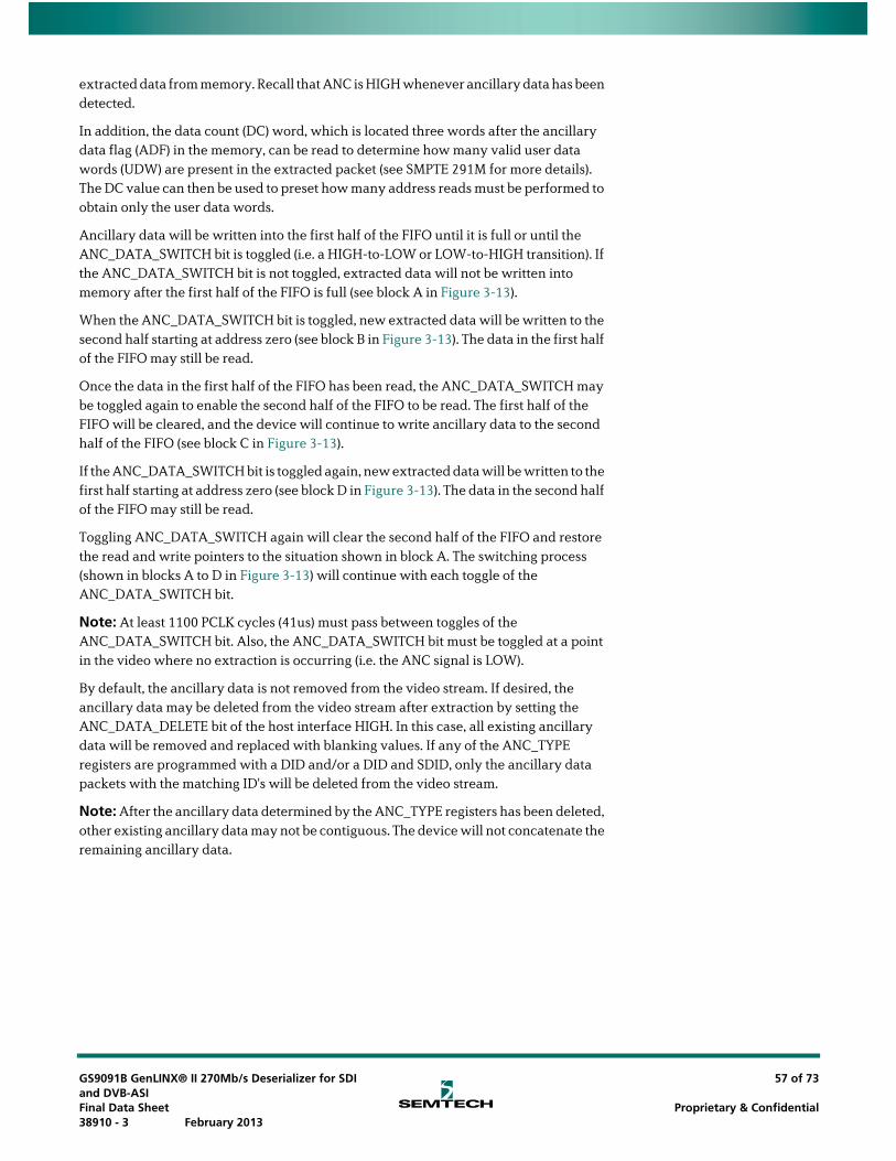
extracted data from memory. Recall that ANC is HIGH whenever ancillary data has been detected.
In addition, the data count (DC) word, which is located three words after the ancillary data flag (ADF) in the memory, can be read to determine how many valid user data words (UDW) are present in the extracted packet (see SMPTE 291M for more details). The DC value can then be used to preset how many address reads must be performed to obtain only the user data words.
Ancillary data will be written into the first half of the FIFO until it is full or until the ANC_DATA_SWITCH bit is toggled (i.e. a HIGH-to-LOW or LOW-to-HIGH transition). If the ANC_DATA_SWITCH bit is not toggled, extracted data will not be written into memory after the first half of the FIFO is full (see block A in Figure 3-13).
When the ANC_DATA_SWITCH bit is toggled, new extracted data will be written to the second half starting at address zero (see block B in Figure 3-13). The data in the first half of the FIFO may still be read.
Once the data in the first half of the FIFO has been read, the ANC_DATA_SWITCH may be toggled again to enable the second half of the FIFO to be read. The first half of the FIFO will be cleared, and the device will continue to write ancillary data to the second half of the FIFO (see block C in Figure 3-13).
If the ANC_DATA_SWITCH bit is toggled again, new extracted data will be written to the first half starting at address zero (see block D in Figure 3-13). The data in the second half of the FIFO may still be read.
Toggling ANC_DATA_SWITCH again will clear the second half of the FIFO and restore the read and write pointers to the situation shown in block A. The switching process (shown in blocks A to D in Figure 3-13) will continue with each toggle of the ANC_DATA_SWITCH bit.
Note: At least 1100 PCLK cycles (41us) must pass between toggles of the ANC_DATA_SWITCH bit. Also, the ANC_DATA_SWITCH bit must be toggled at a point in the video where no extraction is occurring (i.e. the ANC signal is LOW).
By default, the ancillary data is not removed from the video stream. If desired, the ancillary data may be deleted from the video stream after extraction by setting the ANC_DATA_DELETE bit of the host interface HIGH. In this case, all existing ancillary data will be removed and replaced with blanking values. If any of the ANC_TYPE registers are programmed with a DID and/or a DID and SDID, only the ancillary data packets with the matching ID's will be deleted from the video stream.
Note: After the ancillary data determined by the ANC_TYPE registers has been deleted, other existing ancillary data may not be contiguous. The device will not concatenate the remaining ancillary data.
GS9091B GenLINX® II 270Mb/s Deserializer for SDI and DVB-ASIFinal Data Sheet 38910 - 3 February 2013
57 of 73
Proprietary & Confidential
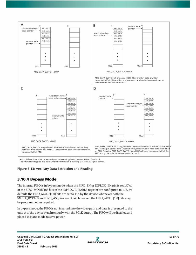
Figure 3-13: Ancillary Data Extraction and Reading
3.10.4 Bypass Mode
The internal FIFO is in bypass mode when the FIFO_EN or IOPROC_EN pin is set LOW, or the FIFO_MODE[1:0] bits in the IOPROC_DISABLE register are configured to 11b. By default, the FIFO_MODE[1:0] bits are set to 11b by the device whenever both the SMPTE_BYPASS and DVB_ASI pins are LOW; however, the FIFO_MODE[1:0] bits may be programmed as required.
In bypass mode, the FIFO is not inserted into the video path and data is presented to the output of the device synchronously with the PCLK output. The FIFO will be disabled and placed in static mode to save power.
%%
ANC_DATA_SWITCH = HIGH
ANC_DATA_SWITCH bit is toggled HIGH. New ancillary data is written to second half of FIFO starting at adress zero. Application layer continues to read from the first half of the FIFO.
Application layerread pointer
Internal writepointer
0
1023 1023
0
Application layerread pointer
Internal writepointer
0 0
1023 1023
ANC_DATA_SWITCH = LOW
0
1023
Internal writepointer
Application layerread pointer
ANC_DATA_SWITCH = HIGH
0
1023
ANC_DATA_SWITCH bit is toggled HIGH. New ancillary data is written to first half ofFIFO starting at address zero. Application layer continues to read from second halfof FIFO. Toggling ANC_DATA_SWITCH back LOW will clear the second half of the FIFO and go back the situation depicted in box A.
Application layerread pointer
Internal writepointer
%%
0
ANC_DATA_SWITCH = LOW
1023
0
1023
ANC_DATA_SWITCH toggled LOW. First half of FIFO cleared and ancillary data read from second half of FIFO. Device continues to write ancillary datato second half of FIFO.
A B
C D
ANC_DATA
ANC_DATA
ANC_DATA
ANC_DATA
ANC_DATA
ANC_DATA
ANC_DATA
ANC_DATA
ANC_DATA
ANC_DATA
ANC_DATA
ANC_DATA
ANC_DATA
ANC_DATA
ANC_DATA
ANC_DATA
ANC_DATA
ANC_DATA
ANC_DATA
ANC_DATA
ANC_DATA
ANC_DATA
ANC_DATA
ANC_DATA
ANC_DATA
ANC_DATA
ANC_DATA
ANC_DATA
NOTE: At least 1100 PCLK cycles must pass between toggles of the ANC_DATA_SWITCH bit.The bit must be toggled at a point where no extraction is occuring (i.e. the ANC signal is LOW).
GS9091B GenLINX® II 270Mb/s Deserializer for SDI and DVB-ASIFinal Data Sheet 38910 - 3 February 2013
58 of 73
Proprietary & Confidential
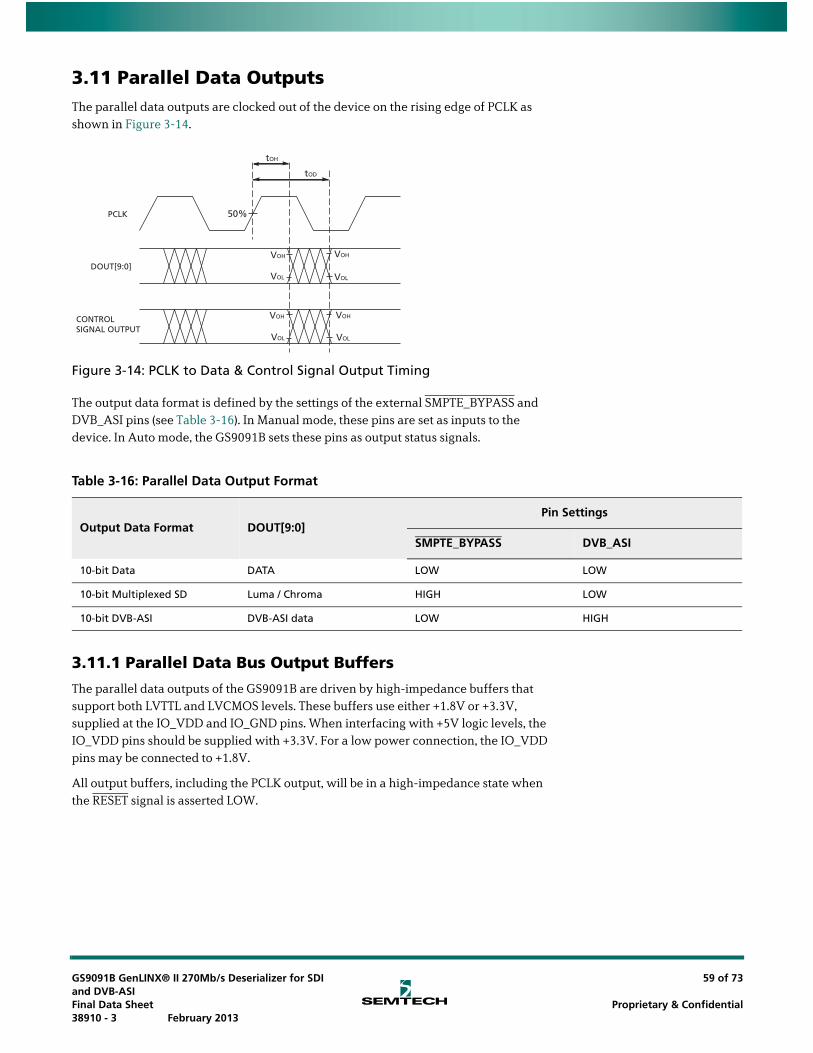
3.11 Parallel Data OutputsThe parallel data outputs are clocked out of the device on the rising edge of PCLK as shown in Figure 3-14.
Figure 3-14: PCLK to Data & Control Signal Output Timing
The output data format is defined by the settings of the external SMPTE_BYPASS and DVB_ASI pins (see Table 3-16). In Manual mode, these pins are set as inputs to the device. In Auto mode, the GS9091B sets these pins as output status signals.
3.11.1 Parallel Data Bus Output Buffers
The parallel data outputs of the GS9091B are driven by high-impedance buffers that support both LVTTL and LVCMOS levels. These buffers use either +1.8V or +3.3V, supplied at the IO_VDD and IO_GND pins. When interfacing with +5V logic levels, the IO_VDD pins should be supplied with +3.3V. For a low power connection, the IO_VDD pins may be connected to +1.8V.
All output buffers, including the PCLK output, will be in a high-impedance state when the RESET signal is asserted LOW.
50%
tOH
tOD
VOH
VOL
VOH
VOL
VOH
VOL
VOH
VOL
CONTROL SIGNAL OUTPUT
DOUT[9:0]
PCLK
Table 3-16: Parallel Data Output Format
Output Data Format DOUT[9:0]Pin Settings
SMPTE_BYPASS DVB_ASI
10-bit Data DATA LOW LOW
10-bit Multiplexed SD Luma / Chroma HIGH LOW
10-bit DVB-ASI DVB-ASI data LOW HIGH
GS9091B GenLINX® II 270Mb/s Deserializer for SDI and DVB-ASIFinal Data Sheet 38910 - 3 February 2013
59 of 73
Proprietary & Confidential
3.11.2 Parallel Output in SMPTE Mode
When the device is operating in SMPTE mode (see Section 3.6), SMPTE data is output on the DOUT[9:0] pins.
3.11.3 Parallel Output in DVB-ASI Mode
When operating in DVB-ASI mode (see Section 3.7), the decoded 8-bit data words will be presented on DOUT[7:0]. DOUT7 = HOUT is the most significant bit of the decoded transport stream data and DOUT0 = AOUT is the least significant bit. DOUT9 will be configured as the DVB-ASI status signal WORDERR and DOUT8 as SYNCOUT. See Section 3.7.2 for a description of these DVB-ASI specific output signals.
3.11.4 Parallel Output in Data-Through Mode
When operating in Data-Through mode (see Section 3.8), the GS9091B presents data to the output data bus without performing any decoding, descrambling, or word-alignment.
3.12 Programmable Multi-Function OutputsThe GS9091B has a 4-pin multi-function output port, STAT[3:0]. Each pin can be programmed to output one of the following signals: H, V, F, FIFO_LD, ANC, EDH_DETECT, FIFO_FULL, and FIFO_EMPTY.
Each of the STAT[3:0] pins can be configured individually using the STAT0_CONFIG[2:0], STAT1_CONFIG[2:0], STAT2_CONFIG[2:0], and STAT3_CONFIG[2:0] registers. Table 3-18 shows the setting of the IO_CONFIG registers for each of the available output signals.
Table 3-17: Output Signals Available on Multi-Function Output Ports
Output Status Signal Reference
H Section 3.6.4
V Section 3.6.4
F Section 3.6.4
FIFO_LD Section 3.9.1
ANC Section 3.9.2
EDH_DETECT Section 3.9.3
FIFO_FULL Section 3.10.2.1
FIFO_EMPTY Section 3.10.2.1
GS9091B GenLINX® II 270Mb/s Deserializer for SDI and DVB-ASIFinal Data Sheet 38910 - 3 February 2013
60 of 73
Proprietary & Confidential
The default setting for each IO_CONFIG register depends on the configuration of the device and the internal FIFO mode selected. This is shown in Table 3-19.
If the programmed signal is not relevant to the current mode of operation, the output will be set to a high-impedance state.
Table 3-18: IO_CONFIG Settings
Function I/O IO_CONFIG Setting
H Output 000b
V Output 001b
F Output 010b
FIFO_LD Output 011b
ANC Output 100b
EDH_DETECT Output 101b
FIFO_FULL Output 110b
FIFO_EMPTY Output 111b
Table 3-19: IO_CONFIG Default Configuration
Device Configuration IO_CONFIG Register
I/O Function Default IO_CONFIG Setting
SMPTE Functionality SMPTE_BYPASS = HIGH DVB_ASI = LOW FIFO: Video Mode or Ancillary Data Extraction Mode
STAT0_CONFIG Output H 000b
STAT1_CONFIG Output V 001b
STAT2_CONFIG Output F 010b
STAT3_CONFIG Output FIFO_LD 011b
DVB-ASI DVB_ASI = HIGH FIFO: DVB-ASI Mode
STAT0_CONFIG Output FIFO_FULL 110b
STAT1_CONFIG Output FIFO_EMPTY 111b
STAT2_CONFIG Output High Z 000b
STAT3_CONFIG Output High Z 000b
Data-Through SMPTE_BYPASS = LOW DVB_ASI = LOW
STAT0_CONFIG Output High Z 000b
STAT1_CONFIG Output High Z 000b
STAT2_CONFIG Output High Z 000b
STAT3_CONFIG Output High Z 000b
GS9091B GenLINX® II 270Mb/s Deserializer for SDI and DVB-ASIFinal Data Sheet 38910 - 3 February 2013
61 of 73
Proprietary & Confidential

3.13 GS9091B Low-latency ModeWhen the IOPROC_EN pin is set LOW, the GS9091B will be set into low-latency mode. The parallel data will be output with the minimum PCLK latency possible. The FIFO and all processing blocks except the descrambling and word alignment blocks will be bypassed when SMPTE_BYPASS is HIGH.
Low-latency mode will also be selected when SMPTE_BYPASS is set LOW, regardless of the setting of the IOPROC_EN signal (see Table 3-20).
In DVB-ASI mode, the device latency is less than in SMPTE mode.
When the GS9091B is configured for low-latency mode, the H,V, and F output timing will be based on the incoming TRS codes as shown in Figure 3-14. Active line-based timing is not available and the setting of the H_CONFIG host interface bit will be ignored.
Figure 3-15: H,V,F Timing In Low-latency Mode
Table 3-20: Pin Settings in Low-latency Mode
IOPROC_EN Setting SMPTE_BYPASS Setting Latency (PCLK Cycles)
LOW LOW 9
HIGH LOW 10
LOW HIGH 10
HIGH HIGH 25
Note: Latency applies to parallel processing core only.
Y/Cr/Cb DATA OUT
PCLK
H
V
F
XYZ(eav)0000003FF XYZ
(sav)0000003FF
GS9091B GenLINX® II 270Mb/s Deserializer for SDI and DVB-ASIFinal Data Sheet 38910 - 3 February 2013
62 of 73
Proprietary & Confidential
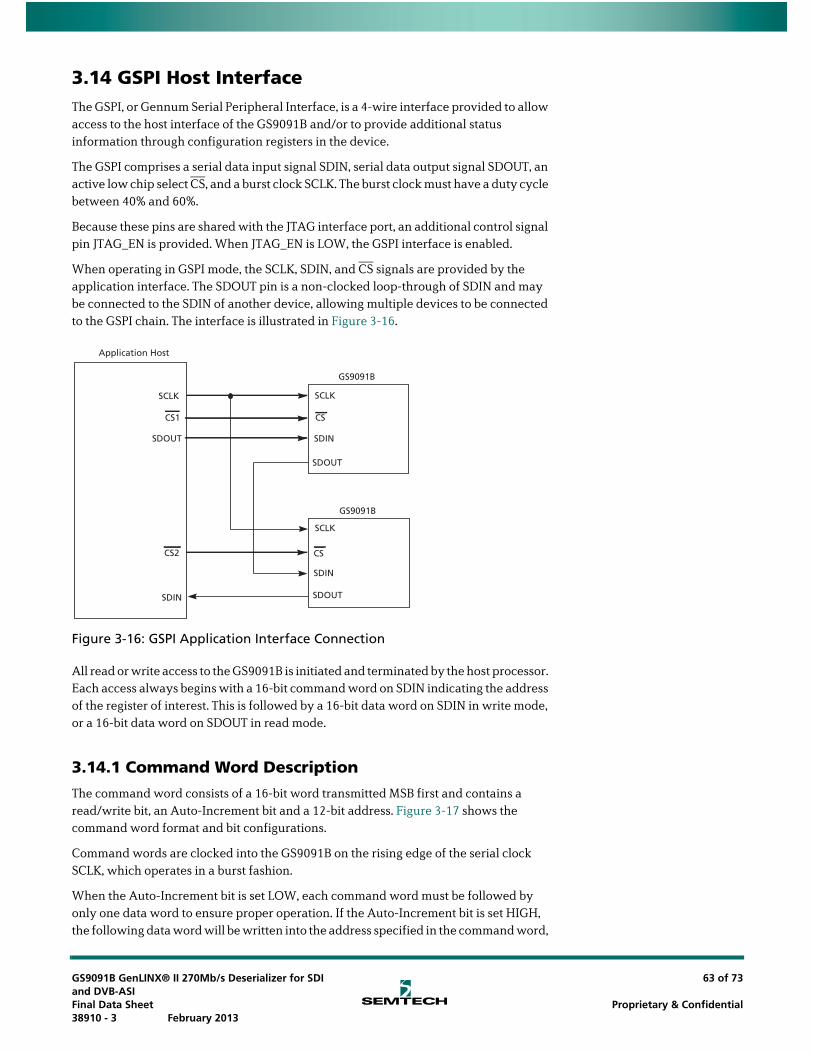
3.14 GSPI Host InterfaceThe GSPI, or Gennum Serial Peripheral Interface, is a 4-wire interface provided to allow access to the host interface of the GS9091B and/or to provide additional status information through configuration registers in the device.
The GSPI comprises a serial data input signal SDIN, serial data output signal SDOUT, an active low chip select CS, and a burst clock SCLK. The burst clock must have a duty cycle between 40% and 60%.
Because these pins are shared with the JTAG interface port, an additional control signal pin JTAG_EN is provided. When JTAG_EN is LOW, the GSPI interface is enabled.
When operating in GSPI mode, the SCLK, SDIN, and CS signals are provided by the application interface. The SDOUT pin is a non-clocked loop-through of SDIN and may be connected to the SDIN of another device, allowing multiple devices to be connected to the GSPI chain. The interface is illustrated in Figure 3-16.
Figure 3-16: GSPI Application Interface Connection
All read or write access to the GS9091B is initiated and terminated by the host processor. Each access always begins with a 16-bit command word on SDIN indicating the address of the register of interest. This is followed by a 16-bit data word on SDIN in write mode, or a 16-bit data word on SDOUT in read mode.
3.14.1 Command Word Description
The command word consists of a 16-bit word transmitted MSB first and contains a read/write bit, an Auto-Increment bit and a 12-bit address. Figure 3-17 shows the command word format and bit configurations.
Command words are clocked into the GS9091B on the rising edge of the serial clock SCLK, which operates in a burst fashion.
When the Auto-Increment bit is set LOW, each command word must be followed by only one data word to ensure proper operation. If the Auto-Increment bit is set HIGH, the following data word will be written into the address specified in the command word,
Application Host
SCLK SCLK
SCLK
CS1
SDOUT SDIN
SDOUT
SDOUT
CS
SDIN
SDIN
CS2
GS9091B
GS9091B
CS
GS9091B GenLINX® II 270Mb/s Deserializer for SDI and DVB-ASIFinal Data Sheet 38910 - 3 February 2013
63 of 73
Proprietary & Confidential
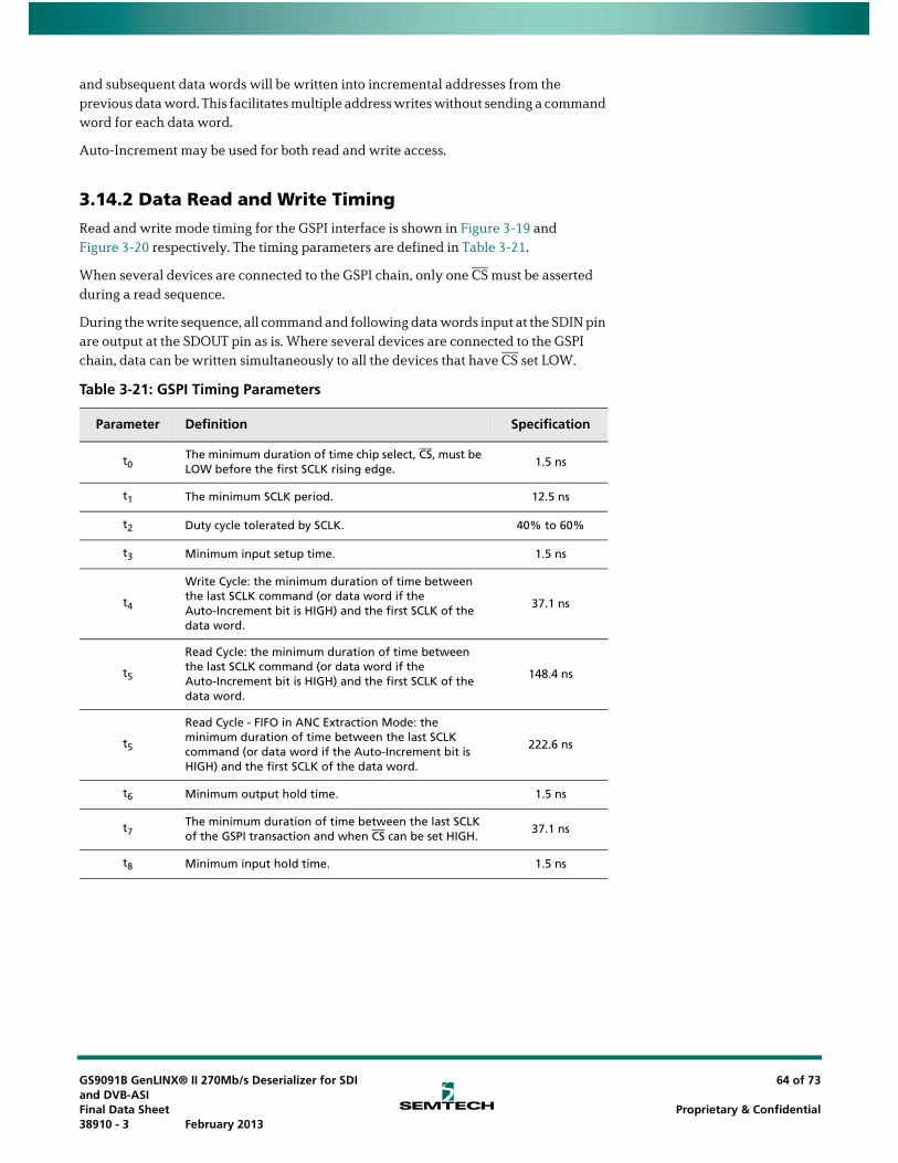
and subsequent data words will be written into incremental addresses from the previous data word. This facilitates multiple address writes without sending a command word for each data word.
Auto-Increment may be used for both read and write access.
3.14.2 Data Read and Write Timing
Read and write mode timing for the GSPI interface is shown in Figure 3-19 and Figure 3-20 respectively. The timing parameters are defined in Table 3-21.
When several devices are connected to the GSPI chain, only one CS must be asserted during a read sequence.
During the write sequence, all command and following data words input at the SDIN pin are output at the SDOUT pin as is. Where several devices are connected to the GSPI chain, data can be written simultaneously to all the devices that have CS set LOW.
Table 3-21: GSPI Timing Parameters
Parameter Definition Specification
t0The minimum duration of time chip select, CS, must be LOW before the first SCLK rising edge.
1.5 ns
t1 The minimum SCLK period. 12.5 ns
t2 Duty cycle tolerated by SCLK. 40% to 60%
t3 Minimum input setup time. 1.5 ns
t4
Write Cycle: the minimum duration of time between the last SCLK command (or data word if the Auto-Increment bit is HIGH) and the first SCLK of the data word.
37.1 ns
t5
Read Cycle: the minimum duration of time between the last SCLK command (or data word if the Auto-Increment bit is HIGH) and the first SCLK of the data word.
148.4 ns
t5
Read Cycle - FIFO in ANC Extraction Mode: the minimum duration of time between the last SCLK command (or data word if the Auto-Increment bit is HIGH) and the first SCLK of the data word.
222.6 ns
t6 Minimum output hold time. 1.5 ns
t7The minimum duration of time between the last SCLK of the GSPI transaction and when CS can be set HIGH.
37.1 ns
t8 Minimum input hold time. 1.5 ns
GS9091B GenLINX® II 270Mb/s Deserializer for SDI and DVB-ASIFinal Data Sheet 38910 - 3 February 2013
64 of 73
Proprietary & Confidential
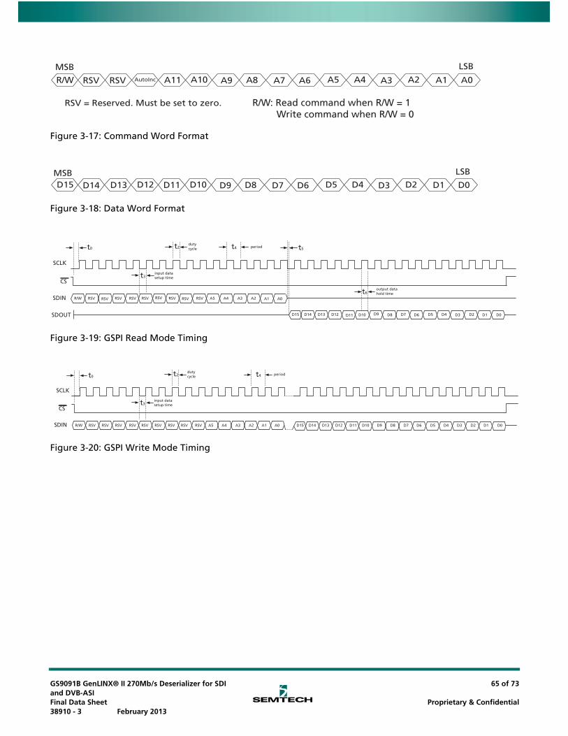
Figure 3-17: Command Word Format
Figure 3-18: Data Word Format
Figure 3-19: GSPI Read Mode Timing
Figure 3-20: GSPI Write Mode Timing
MSB LSB
A4A5A6A8 A7A9 A3 A2 A1 A0A10A11AutoIncRSVRSVR/W
RSV = Reserved. Must be set to zero. R/W: Read command when R/W = 1 Write command when R/W = 0
MSB LSB
D4D5D6D8 D7D9 D3 D2 D1 D0D10D11D12D13D14D15
SDOUT
R/W RSV RSV A0A1A2A3A4A5RSVRSVRSVRSVRSVRSV
D15 D14 D13 D12 D0D1D2D3D4D5D6D7D8D9D11 D10
SCLK
CS
SDIN RSV
t0 t2
t3input data setup time
dutycycle t4 period t5
t6output datahold time
R/W RSV RSV A0A1A2A3A4A5RSVRSVRSVRSVRSVRSV D15 D14 D13 D12 D0D1D2D3D4D5D6D7D8D9D11 D10
SCLK
CS
SDIN RSV
t0 t2
t3input data setup time
dutycycle t4 period
GS9091B GenLINX® II 270Mb/s Deserializer for SDI and DVB-ASIFinal Data Sheet 38910 - 3 February 2013
65 of 73
Proprietary & Confidential
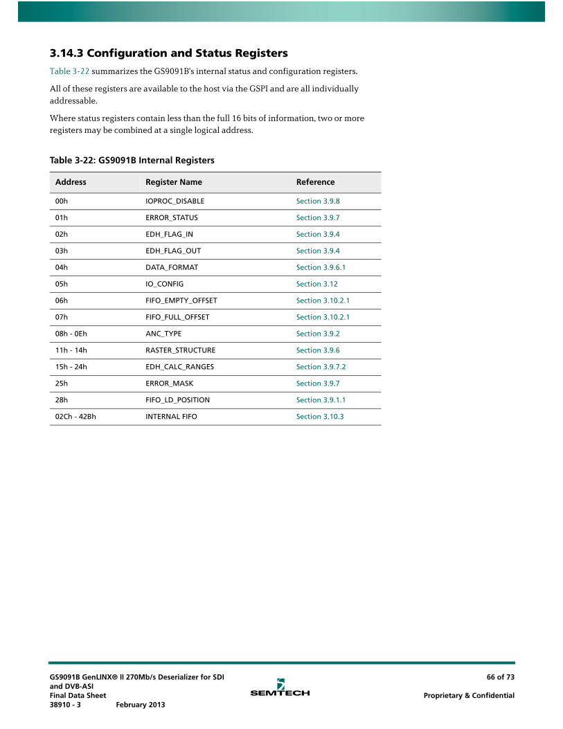
3.14.3 Configuration and Status Registers
Table 3-22 summarizes the GS9091B's internal status and configuration registers.
All of these registers are available to the host via the GSPI and are all individually addressable.
Where status registers contain less than the full 16 bits of information, two or more registers may be combined at a single logical address.
Table 3-22: GS9091B Internal Registers
Address Register Name Reference
00h IOPROC_DISABLE Section 3.9.8
01h ERROR_STATUS Section 3.9.7
02h EDH_FLAG_IN Section 3.9.4
03h EDH_FLAG_OUT Section 3.9.4
04h DATA_FORMAT Section 3.9.6.1
05h IO_CONFIG Section 3.12
06h FIFO_EMPTY_OFFSET Section 3.10.2.1
07h FIFO_FULL_OFFSET Section 3.10.2.1
08h - 0Eh ANC_TYPE Section 3.9.2
11h - 14h RASTER_STRUCTURE Section 3.9.6
15h - 24h EDH_CALC_RANGES Section 3.9.7.2
25h ERROR_MASK Section 3.9.7
28h FIFO_LD_POSITION Section 3.9.1.1
02Ch - 42Bh INTERNAL FIFO Section 3.10.3
GS9091B GenLINX® II 270Mb/s Deserializer for SDI and DVB-ASIFinal Data Sheet 38910 - 3 February 2013
66 of 73
Proprietary & Confidential
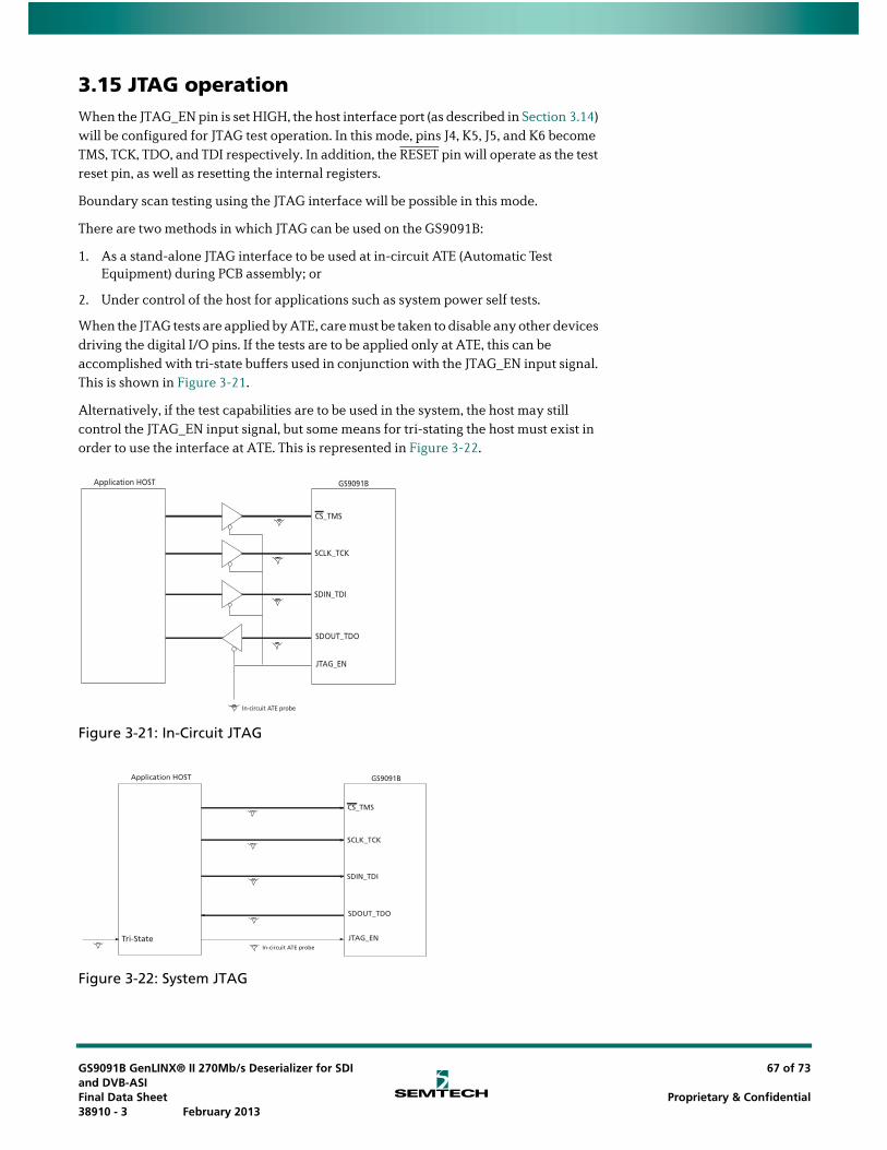
3.15 JTAG operationWhen the JTAG_EN pin is set HIGH, the host interface port (as described in Section 3.14) will be configured for JTAG test operation. In this mode, pins J4, K5, J5, and K6 become TMS, TCK, TDO, and TDI respectively. In addition, the RESET pin will operate as the test reset pin, as well as resetting the internal registers.
Boundary scan testing using the JTAG interface will be possible in this mode.
There are two methods in which JTAG can be used on the GS9091B:
1. As a stand-alone JTAG interface to be used at in-circuit ATE (Automatic Test Equipment) during PCB assembly; or
2. Under control of the host for applications such as system power self tests.
When the JTAG tests are applied by ATE, care must be taken to disable any other devices driving the digital I/O pins. If the tests are to be applied only at ATE, this can be accomplished with tri-state buffers used in conjunction with the JTAG_EN input signal. This is shown in Figure 3-21.
Alternatively, if the test capabilities are to be used in the system, the host may still control the JTAG_EN input signal, but some means for tri-stating the host must exist in order to use the interface at ATE. This is represented in Figure 3-22.
Figure 3-21: In-Circuit JTAG
Figure 3-22: System JTAG
Application HOST GS9091B
CS_TMS
SCLK_TCK
SDIN_TDI
SDOUT_TDO
JTAG_EN
In-circuit ATE probe
Application HOST GS9091B
CS_TMS
SCLK_TCK
SDIN_TDI
SDOUT_TDO
JTAG_ENIn-circuit ATE probe
Tri-State
GS9091B GenLINX® II 270Mb/s Deserializer for SDI and DVB-ASIFinal Data Sheet 38910 - 3 February 2013
67 of 73
Proprietary & Confidential

3.16 Device Power UpThe GS9091B has a recommended power supply sequence. To ensure correct power up, power the CORE_VDD pins before the IO_VDD pins. In order to initialize all internal operating conditions to their default state the application layer must hold the RESET pin LOW for a minimum of treset = 1ms. (See Figure 3-23)
Device pins can be driven prior to power up without causing damage.
Figure 3-23: Reset pulse
CORE_VDD
RESET
treset
+1.71V+1.8V
Reset Reset
treset
GS9091B GenLINX® II 270Mb/s Deserializer for SDI and DVB-ASIFinal Data Sheet 38910 - 3 February 2013
68 of 73
Proprietary & Confidential
4. References & Relevant Standards
Table 4-1: References and Relevant Standards
SMPTE 125M Component video signal 4:2:2 – bit parallel interface
SMPTE 259M10-Bit 4:2:2 Component and 4fSC Composite Digital Signals - Serial Digital Interface
SMPTE 291M Ancillary Data Packet and Space Formatting
SMPTE 293M720 x 483 active line at 59.94 Hz progressive scan production – digital representation
SMPTE 305.2M Serial Data Transport Interface
SMPTE 352M Video Payload Identification for Digital Television Interfaces
SMPTE RP165Error Detection Checkwords and Status Flags for Use in Bit-Serial Digital Interfaces for Television
SMPTE RP168Definition of Vertical Interval Switching Point for Synchronous Video Switching
GS9091B GenLINX® II 270Mb/s Deserializer for SDI and DVB-ASIFinal Data Sheet 38910 - 3 February 2013
69 of 73
Proprietary & Confidential
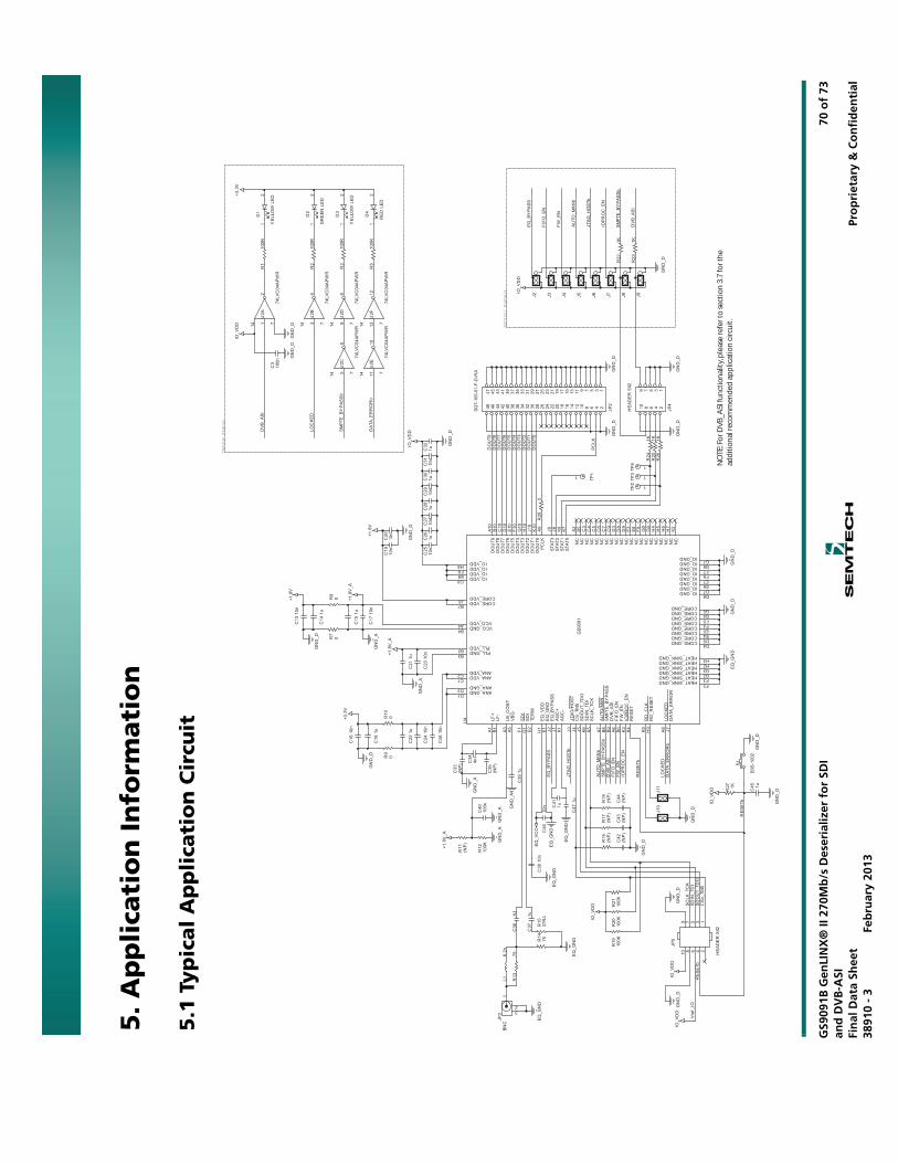
GS9
091B
Gen
LIN
X®
II 2
70M
b/s
Des
eria
lizer
fo
r SD
I an
d D
VB
-ASI
Fin
al D
ata
Shee
t
3891
0 -
3Fe
bru
ary
2013
70 o
f 73
Pro
pri
etar
y &
Co
nfi
den
tial
5. A
pp
lica
tio
n I
nfo
rmati
on
5.1
Ty
pic
al
Ap
pli
cati
on
Cir
cuit
C47
1uJT
AG
_HO
STb
LF+
A1
LF-
B1
EQ
_GN
DE
1
SD
IF
1
SD
IG
1
TER
ME
2
EQ
_VD
DH
1
AG
C+
J1
AG
C-
K1
EQ
_BY
PA
SS
J2
DO
UT9
A10
DO
UT8
B10
DO
UT7
C10
DO
UT6
D10
DO
UT5
E10
DO
UT4
F10
DO
UT3
G10
DO
UT2
H10
DO
UT1
J10
DO
UT0
K10
AU
TO/M
AN
A7
SM
PTE
_BY
PA
SS
B8
DV
B_A
SI
B9
VB
GA
5
FIF
O_E
NA
6
CORE_VDDB7
IOP
RO
C_E
NK
3
JTA
G/H
OS
TJ3
CS
_TM
SJ4
SD
OU
T_TD
OJ5
SD
IN_T
DI
K6
SC
LK_T
CK
K5
STA
T0K
7S
TAT1
K8
STA
T2J8
STA
T3J9
PC
LKA
9
RE
SE
TK
4
LOC
KE
DA
8
DA
TA_E
RR
OR
J7
HEAT_SINK_GNDF2
HEAT_SINK_GNDF3
HEAT_SINK_GNDG2
HEAT_SINK_GNDG3
HEAT_SINK_GNDH2
HEAT_SINK_GNDH3
CORE_GNDD4
CORE_GNDD5
CORE_GNDE4
CORE_GNDE5
CORE_GNDF4
CORE_GNDF5
CORE_GNDG4
CORE_GNDG5
IO_GNDD6
IO_GNDD7
IO_GNDE6
IO_GNDE7
IO_GNDF6
IO_GNDF7
IO_GNDG6
IO_GNDG7
IO_VDDC8
IO_VDDE9
IO_VDDF9
IO_VDDH8
FW
_EN
B6
CORE_VDDJ6
LB_C
ON
TA
3
PLL_VDDB2 PLL_GNDB3
VCO_VDDA4 VCO_GNDB4
NC
A2
NC
B5
NC
C3
NC
C4
NC
C5
NC
C6
NC
C7
NC
C9
NC
D3
NC
D8
NC
D9
NC
E3
NC
E8
NC
F8
NC
G8
NC
G9
NC
H4
NC
H5
NC
H6
NC
H7
NC
K2
RD
_CLK
K9
RD
_RE
SE
TH
9
ANA_VDDC1
ANA_VDDC2
ANA_GNDD1
ANA_GNDD2
U4
GS
9091
C38
10n
C39
1u
GN
D_A
R14
75
L16.
2n
EQ
_GN
D
C37
1u
1
TP4
R13
75
1
TP3
R15
37R
4
1
TP2
C36
1U
1
32
JP3
BN
C
1
TP1
EQ
_GN
D
GN
D_D
R10
0
EQ
_GN
D
C16
10n
C24
10n
R9
0
+3.3
V
C18
1u
C22
1u
EQ
_GN
D
GN
D_D
GN
D_D
EQ
_VC
C
J8
DV
B_A
SI
J9
R22
1K
J11
SM
PTE
_BY
PA
SS
b
12
34
56
78
910
1112
1314
1516
1718
1920
2122
2324
2526
2728
2930
3132
3334
3536
3738
3940
4142
4344
4546
4748 JP
2
SQ
T-10
5-01
-F-D
-RA
GN
D_DJ1
0G
ND
_D
IO_V
DD
AU
TO_M
AN
b
JTA
G_H
OS
Tb
IOP
RO
C_E
N
FIF
O_E
N
FW
_EN
Control Signals
R23
1K
J7G
ND
_D
J3
GN
D_D
J4 J5 J6
12
34
56
78
910 JP
4
HE
AD
ER
5X2
GN
D_D
+1.8
V_A
R16
(NP
)
GN
D_D
R8
0
C42
(NP
)
C13
10n
GN
D_D
R18
(NP
)
C17
10n
C44
(NP
)
DO
UT9
R7
0
R17
(NP
)
C43
(NP
)
+1.8
V
C14
1u
C15
1u
GN
D_A
DO
UT8
J2
DO
UT7
EQ
_BY
PA
SS
C35
(NP
)
C33
(NP
) C34
4n7
DO
UT6
+1.8
V_A
DO
UT5
C23
10n
GN
D_A
GN
D_A
C21
1u
DO
UT4
IO_V
DD
IO_V
DD
C48
10n
98
14 7
U2D
74LV
C04
AP
WR
RE
SE
Tb
R1
100R
1312
14 7
U2F
74LV
C04
AP
WR
SM
PTE
_BY
PA
SS
b
246810
13579
JP5
HE
AD
ER
5X2
21
D2
GR
EE
N L
ED
21
D1
YE
LLO
W L
ED
GN
D_D
RE
SE
Tb
Vre
f_IOG
ND
_D
12
14 7
U2A
74LV
C04
AP
WR
DO
UT3
34
14 7
U2B
74LV
C04
AP
WR
56
14 7
U2C
74LV
C04
AP
WR
R2
100R
R3
100R
R5
100R
DA
TA_E
RR
OR
b
GN
D_D
Device Status
IO_V
DD
+3.3
V
C3
100n
1110
14 7
U2E
74LV
C04
AP
WR
GN
D_D
DV
B_A
SI
DO
UT2
21
D3
YE
LLO
W L
ED 2
1D
4
RE
D L
ED
LOC
KE
D
DO
UT1
DO
UT0
GN
D_D
+1.8
V
C19
10n
PC
LK
R21
100K
R20
100K
R19
100K
IO_V
DD
C20
10n
GN
D_D
CS
b_TM
SS
DO
UT_
TDO
SD
IN_T
DI
GN
D_D
C31
10n
C32
1u
IO_V
DD
R24
1KR
251K
R26
1K
SC
LK_T
CK
C29
10n
C30
1uC
2710
nC
281u
C25
10n
C26
1u
EQ
_BY
PA
SS
AU
TO_M
AN
b
R28
0
SM
PTE
_BY
PA
SS
bD
VB
_AS
I
EQ
_GN
D
FIF
O_E
N
C45 1u
IO_V
DD
S1
B3S
-100
2
C46
10n
R27 1K
GN
D_D
GN
D_D
FW
_EN
IOP
RO
C_E
N
GN
D_A
GN
D_A
R11
(NP
)
+1.8
V_A
C40
100n
R12
100K
RE
SE
Tb
EQ
_GN
D
LOC
KE
DD
ATA
_ER
RO
Rb
C41
1u
NO
TE: F
or D
VB
_ASI
fun
ctio
nal
ity,
ple
ase
refe
r to
sec
tio
n 3
.7 fo
r th
e ad
dit
ion
al re
com
men
ded
ap
plic
atio
n c
ircu
it.

6. Package & Ordering Information
6.1 Package Dimensions
Figure 6-1: Packaging Dimensions
* THE BALL DIAMETER, BALL PITCH, STAND-OFF & PACKAGE THICKNESS
ARE DIFFERENT FROM JEDEC SPEC M0192 (LOW PROFILE BGA FAMILY)
BOTTOM VIEWTOP VIEW
11±
0.10
9.00
1.00
11 ± 0.10
9.00
1.00
10 9 8 7 6 5 4 3 2 1
A
B
C
D
E
F
G
H
J
K
H
K
J
D
F
G
E
C
B
A
109876542 31PIN 1 CORNER
PIN 1 CORNER
-A-
0.20(4X)
-B-
Ø0.25 S C A B
Ø0.10 S C
Ø0.40~0.60(100X)
0.25
C
0.70
±0.
05(0
.61)
-C- SEATING PLANE
0.15
0.30
~0.
50
1.71
REF
.
Ball Pitch :
Ball Diameter : Mold Thickness :
Substrate Thickness :
1.00
0.50
0.61
0.70
GS9091B GenLINX® II 270Mb/s Deserializer for SDI and DVB-ASIFinal Data Sheet 38910 - 3 February 2013
71 of 73
Proprietary & Confidential
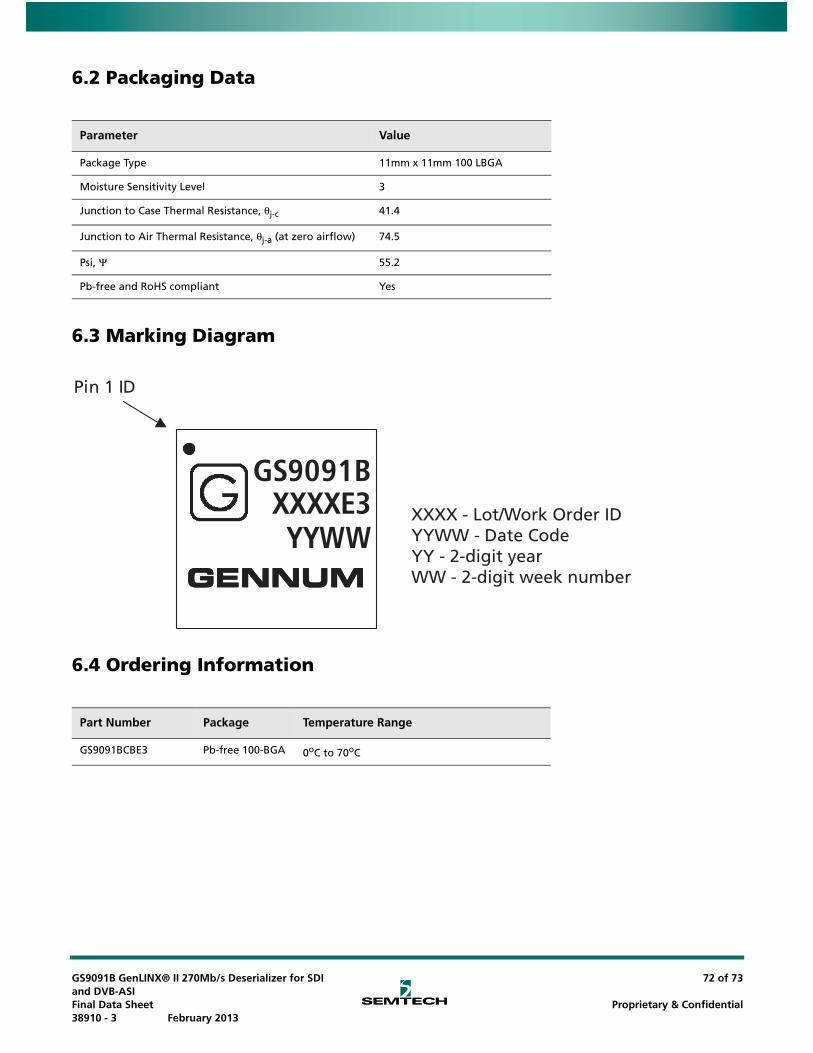
6.2 Packaging Data
6.3 Marking Diagram
6.4 Ordering Information
Parameter Value
Package Type 11mm x 11mm 100 LBGA
Moisture Sensitivity Level 3
Junction to Case Thermal Resistance, θj-c 41.4
Junction to Air Thermal Resistance, θj-a (at zero airflow) 74.5
Psi, Ψ 55.2
Pb-free and RoHS compliant Yes
Pin 1 ID
GS9091BXXXXE3YYWW
XXXX - Lot/Work Order IDYYWW - Date CodeYY - 2-digit yearWW - 2-digit week number
Part Number Package Temperature Range
GS9091BCBE3 Pb-free 100-BGA 0oC to 70oC
GS9091B GenLINX® II 270Mb/s Deserializer for SDI and DVB-ASIFinal Data Sheet 38910 - 3 February 2013
72 of 73
Proprietary & Confidential
© Semtech 2012
All rights reserved. Reproduction in whole or in part is prohibited without the prior written consent of the copyright owner. The information presented in this document does not form part of any quotation or contract, is believed to be accurate and reliable and may be changed without notice. No liability will be accepted by the publisher for any consequence of its use. Publication thereof does not convey nor imply any license under patent or other industrial or intellectual property rights. Semtech assumes no responsibility or liability whatsoever for any failure or unexpected operation resulting from misuse, neglect improper installation, repair or improper handling or unusual physical or electrical stress including, but not limited to, exposure to parameters beyond the specified maximum ratings or operation outside the specified range.
SEMTECH PRODUCTS ARE NOT DESIGNED, INTENDED, AUTHORIZED OR WARRANTED TO BE SUITABLE FOR USE IN LIFE-SUPPORT APPLICATIONS, DEVICES OR SYSTEMS OR OTHER CRITICAL APPLICATIONS. INCLUSION OF SEMTECH PRODUCTS IN SUCH APPLICATIONS IS UNDERSTOOD TO BE UNDERTAKEN SOLELY AT THE CUSTOMER’S OWN RISK. Should a customer purchase or use Semtech products for any such unauthorized application, the customer shall indemnify and hold Semtech and its officers, employees, subsidiaries, affiliates, and distributors harmless against all claims, costs damages and attorney fees which could arise.
Notice: All referenced brands, product names, service names and trademarks are the property of their respective owners.
DOCUMENT IDENTIFICATIONFINAL DATA SHEETInformation relating to this product and the application or design described herein is believed to be reliable, however such information is provided as a guide only and Semtech assumes no liability for any errors in this document, or for the application or design described herein. Semtech reserves the right to make changes to the product or this document at any time without notice.
GS9091B GenLINX® II 270Mb/s Deserializer for SDI and DVB-ASIFinal Data Sheet 38910 - 3 February 2013
73 of 7373
Proprietary & Confidential
Contact Information
Semtech CorporationGennum Products Division
200 Flynn Road, Camarillo, CA 93012Phone: (805) 498-2111, Fax: (805) 498-3804
www.semtech.com
CAUTIONELECTROSTATIC SENSITIVE DEVICES
DO NOT OPEN PACKAGES OR HANDLE EXCEPT AT A STATIC-FREE WORKSTATION