gs-dl020 - sequential digital logic trainer
TRANSCRIPT

Copyright © 2011 by Enoch Hwang, Ph.D. and Global Specialties ®
All rights reserved.
Printed in Taiwan.
No part of this publication may be reproduced, stored in a retrieval system or transmitted, in any form
or by any means, electronic, mechanical, photocopying, recording or otherwise, without the prior
written permission of the author.

Sequential Logic Design
Table of Contents Page
Chapter 1 Sequential Logic Design Trainer, Model DL-020 .............................................................. 1
Chapter 2 Microprocessors ................................................................................................................. 5
Section 2.1 Introduction to Microprocessors ............................................................................. 5
Section 2.2 Combinational and Sequential Circuit Analogy ..................................................... 8
Chapter 3 Sequential Logic Circuits ................................................................................................... 9
Section 3.1 Identifying Sequential Circuits ................................................................................ 9
Section 3.2 Analysis of Sequential Circuits ................................................................................. 9
Section 3.3 Finite State Machines ............................................................................................. 11
Section 3.4 Synthesis of Sequential Circuits ............................................................................. 12
Chapter 4 Labs .................................................................................................................................. 17
Section 4.1 Lab 1: The NAND gate ............................................................................................ 17
Section 4.2 Lab 2: SR Latch ........................................................................................................ 21
Section 4.3 Lab 3: D Latch ......................................................................................................... 25
Section 4.4 Lab 4: D Latch with Enable .................................................................................... 27
Section 4.5 Lab 5: D Flip-Flop .................................................................................................... 29
Section 4.6 Lab 6: D Flip-Flop with Enable ............................................................................... 35
Section 4.7 Lab 7: Register ........................................................................................................ 37
Section 4.8 Lab 8: Binary Up Counter ....................................................................................... 39
Section 4.9 Lab 9: Car Security System Version 2 ..................................................................... 41
Section 4.10 Lab 10: Rotating Lights Controller ...................................................................... 45
Section 4.11 Lab 11: Jeopardy® Contestant Response Controller .......................................... 53
Section4.12Lab12:TrafficLightController ............................................................................ 57


Chapter 1 Sequential Logic Design Trainer, Model DL-020
www.globalspecialties.com 1
Chapter 1
Sequential Logic Design Trainer, Model DL-020The Sequential Logic Design Trainer that you have contains all of the necessary tools for you to
easily implement many combinational and sequential digital logic circuits. Combinational and se-
quential logic circuits are the two major types of circuits found inside microprocessors. The layout of
the trainer is shown in Figure 1.
Figure 1: Sequential Logic Design Trainer layout. All of the logic gates and I / O’s are pre-mounted with wire connection points.
The following is a list of all of the components on the trainer:
> Twelve NOT gates
> Eight 4-input AND gates
> Twelve 2-input AND gates
> Eight 4-input OR gates
> Eight 2-input OR gates

Sequential Logic Design
Global Specialties 2
> Twelve 2-input XOR gates
> Eight 2-input NAND gates
> FourDflip-flopswithenableandasynchronousclear
> Four 4-to-1 multiplexers
> Selectable 1 Hz/20 Hz clock
> Eight multi-color LEDs
> Two 7-segment LED displays
> Eight toggle switches
> Three push button switches
> VCC and GND connection points
> General bread board area with 270 tie points
> Hook-up wires of various lengths
The eight LEDs and the LED segments of the 7-segment displays are active high, which means that
a logic 1 will turn the light on, and a logic 0 will turn the light off. The three push buttons, PB0, PB1
and PB2, are also active high, so pressing the button will produce a logic 1 signal. All of the eight
switches,SW0toSW7,areconfiguredsothatwhentheswitchisintheuppositiontheoutputisa
logic 1, and when the switch is in the down position the output is a logic 0.
You can also connect a wire to one of the VCC connection points to directly get a logic 1 signal.
Similarly, connecting a wire to one of the GND connection points will get a logic 0 signal.
InadditiontothestandardlogicgatesandI/O’s,thetraineralsoprovidesfourDflip-flopswith
enable and asynchronous clear for building larger sequential circuits. Sequential circuits in a com-
puter system also require precise timing, and this is accomplished by using a clock signal which is a
square-waveofafixedfrequency.Thetrainerhasasquarewaveclockgeneratorfortwodifferent
frequencies,1Hzand20Hz,selectableusingatoggleswitch.Theuseoftheflip-flopsandtheclock
will be explained in detail in later sections of this manual. Finally, the trainer also includes four 4-to-1
multiplexers for building larger circuits.
Allofthelogicgates,flip-flops,multiplexersandI/O’sarepre-mountedforeasywiringofacircuit.
All component inputs are connected to one wire connection point, and all component outputs have
multiple wire connection points. To connect from the output of a component to the input of another
component, simply use a hook-up wire to connect between the two wire connection points. For
example, push button PB0 has six common wire connection points, so to use PB0 you can connect a
wire to any one of these six connection points. Connect the other end of the hook-up wire to the one
connection point for LED0. When you press the push button, the LED should turn on. Try this simple
connection now to see that it works.
The logic gates on the trainer are also numbered for easy reference for when connecting a circuit
up. For instance, the eight 4-input AND gates are numbered from 1 to 8. There are also eight 4-input
OR gates, and they are also numbered from 1 to 8. So be careful when a circuit diagram says gate
number 1 that you know which type of gate it is referring to, i.e., whether it is the 4-input AND gate,

Chapter 1 Sequential Logic Design Trainer, Model DL-020
www.globalspecialties.com 3
the 4-input OR gate or even one of the other gates. For example, the following circuit diagram uses
the number-1 4-input AND gate, the number-2 2-input AND gate and the number-6 2-input OR gate.
In this courseware, we will use the notation 4-AND#1, 2-AND#2 and 2-OR#6 to refer to these three
gates respectively. 16
2
The general breadboard area allows you to connect other components that are not available on
the trainer together with your circuit. The breadboard consists of many holes for you to connect
hook-up wires and integrated circuit (IC) chips. All of the holes are already connected together in
groups. This way, you can connect two wires together (or connect a wire to an IC pin) simply by plug-
ging the two wires into two holes that are already connected together. The layout of the breadboard
is shown in Figure 2.
Section 1
Section 2
Section 3
Section 4
Figure 2: Breadboard layout. The holes in section 1 are connected horizontally. The holes in sec-tion 2 are connected vertically. The holes in section 3 are connected vertically. The holes in section 4 are connected horizontally. Holes in any two different sections are not connected.
There are four general sections on the breadboard. All of the holes in section 1 are connected in
common horizontally. The holes in this section are usually connected to VCC to provide power or the
logic 1 signal to your circuit on the breadboard. Like section 1, all of the holes in section 4 are also
connected in common horizontally. The holes in this section are usually connected to GND to provide
a common ground or the logic 0 signal to your circuit. The holes in section 2 are connected vertically,
sothefiveholesineachcolumnareconnectedincommon,buttheverticalcolumnsarenotconnected
together.Theholesinsection3arealsoconnectedverticallylikethoseinsection2,sothefiveholes
in each column are connected in common, but the vertical columns between section 2 and section 3
are not connected together. Finally, holes in any two different sections are not connected together.
In the case where you might need more connection points for a component on the trainer, you can
use the breadboard to give you extra connection points. Typically, you use a breadboard to connect
wires to an IC chip. A standard dual-in-line (DIP) IC chip would be plugged into the breadboard with
one row of pins in section 2 and the second row of pins in section 3.

Sequential Logic Design
Global Specialties 4
Figure 1A: DL-020 trainer with three jumper wires.
Let us now test out the trainer. The three thick lines in Figure 1A show three wires connected from
the two switches, SW0 and SW1, to the inputs of the number-8 2-input NAND gate, and the output
of this NAND gate is connected to LED0. In a schematic circuit drawing, this circuit would be shown
as follows
SW1SW0
LED08
Using three pieces of hook-up wires, make these same connections now on your trainer. Slide the
two switches up and down and see how the LED turns on and off. At this point you may not under-
standwhytheLEDturnsonandoffthewayitdoes.Justkeepreadingandyouwillfindoutvery
quickly, and you will be well on your way to designing your very own microprocessors.

Chapter 2 Microprocessors
www.globalspecialties.com5
Chapter 2
Introduction to Microprocessors
2.1. Introduction to Microprocessors
Whether you like it or not, microprocessors (also known as microcontrollers) control many aspects
of our lives today – either directly or indirectly. In the morning, a microcontroller inside your alarm
clock wakes you up, and another microcontroller adjusts the temperature in your coffee pot and
alerts you when your coffee is ready. When you turn on the TV for the morning news, it is a microcon-
troller that controls the operation of the TV such as adjusting the volume and changing the channel.
A microcontroller opens your garage door, and another inside your car releases your anti-lock break
whenyoudriveyourcarout.Atthetrafficlight,amicrocontrollersensestheflowoftrafficandturns
on (hopefully) the green light for you when you reach the intersection. You stop by a gas station and
a microcontroller reads and accepts your credit card, and let you pump your gas. When you walk up
toyourofficebuilding,asensorsensesyourpresenceandinformsamicrocontrollertoopentheglass
door for you. You press button eight inside the elevator, and a microprocessor controls the elevator to
take you up to the 8thfloor.Duringlunchbreak,youstopbyagiftshoptobuyamusicalbirthdaycard
forafriendandfindoutthatthebirthdaysongisbeinggeneratedbyamicroprocessorthatlookslike
a dried-up pressed-down piece of gum inside the card. I can continue on with this list of things that
are controlled by microprocessors, but I think you got the idea. Oh, one last example, do you know
that it is also a microprocessor that is at the heart of your personal computer, whether it is a PC or a
Mac? That’s right the Intel Duo Core® CPU inside a PC is a general-purpose microprocessor.
So you see, microprocessors are at the heart of all “smart” devices, whether they be electronic de-
vices or otherwise, and their smartness comes as a direct result of the decisions and controls that the
microprocessors make. In this three part award-winning series on microprocessor design training kits,
you will learn how to design and actually implement real working custom microprocessors. Designing
and building microprocessors may sound very complicated, but don’t let that scare you, because it is
notreallyallthatdifficulttounderstandthebasicprinciplesofhowmicroprocessorsaredesigned.
After you have learned the materials presented in these labs, you will have the basic knowledge of
how microprocessors are designed, and be able to design and implement your very own custom mi-
croprocessors!
There are generally two types of microprocessors: general-purpose microprocessors and dedicated
microprocessors. General-purpose microprocessors, such as the Intel Pentium® CPU, can perform dif-
ferent tasks under the control of software instructions. General-purpose microprocessors are used in
all personal computers.
Dedicated microprocessors, also known as microcontrollers, on the other hand, are designed to
performjustonespecifictask.Soforexample,insideyourcellphone,thereisadedicatedmicropro-
cessor that controls its entire operation. The embedded microprocessor inside the cell phone does
nothing else but controls the operation of the phone. Dedicated microprocessors are therefore usu-

Sequential Logic Design
Global Specialties 6
ally much smaller, and not as complex as general-purpose microprocessors. Although the small dedi-
cated microprocessors are not as powerful as the general-purpose microprocessors, they are being
sold and used in a lot more places than the powerful general-purpose microprocessors that are used
in personal computers.
The electronic circuitry inside a microprocessor is called a digital logic circuit or just digital circuit,
as opposed to an analog circuit. Digital circuits deal with just two discrete values, usually represented
by either a 0 or a 1, whereas analog circuits deal with a continuous range of values. The main com-
ponents in an analog circuit usually consist of discrete resistors, capacitors, inductors, and transistors,
whereas the main components in a digital circuit consist of the AND, OR and NOT logic gates. From
these three basic types of logic gates, the most powerful computer can be made. Logic gates are built
using transistors—the fundamental active component for all digital logic circuits. Transistors are just
electronic binary switches that can be turned on or off. The two binary values, 1 and 0, are used to
represent the on and off states of a transistor. So instead of having to deal with different voltages and
currents as in analog circuits, digital circuits only deal with the two abstract values of 0 and 1. Hence,
it is usually easier to design digital circuits than analog circuits.
Figure 3 (a) is a picture of a discrete transistor. Above the transistor is a shiny piece of raw silicon
which is the main ingredient for making transistors. As you can see in the picture, the transistor has
three connections: one for the signal input, one for the signal output, and one for turning on and
off the transistor. Figure 3 (b) is a picture of hundreds of transistors inside an integrated circuit (IC)
chipasviewedthroughanelectronmicroscope.Therighthalfofthepictureisamagnificationofthe
rectangle area in the left half. Each junction is a transistor.
(a) (b)
Figure 3: Pictures of transistors: (a) a discrete transistor with a piece of silicon; (b) hundreds of transistors inside an IC chip as viewed through an electron microscope. The right half of the picture is a magnification of the rectangle area in the left half.
Figure 4 is a picture with several generations of integrated circuit chips. Going clockwise from the
top-left corner is a lump of silicon which can be used to make many transistors; an Intel® 8085 micro-
processor with its top opened. The 8085 is an 8-bit general-purpose microprocessor with a maximum
clock speed of around 10 MHz, and contains around 29,000 transistors; an Intel® 486 DX microproces-
sor. The 486 has a maximum clock speed of 100 MHz and contains around 1.2 million transistors; the
2732 erasable-programmable-read-only-memory (EPROM) which has a non-volatile storage capacity
of 4,096 bytes. The 2732 contains around 32,000 transistors; the tip of a pen which contains no transis-
tor;the7440chipwhichhastwo4-inputNANDgatesandcontains20transistors;andfinallyasingle
discrete transistor.

Chapter 2 Microprocessors
www.globalspecialties.com7
Figure 4: Picture of various integrated circuit chips. Going clockwise from the top-left corner is a lump of silicon, an eight-bit Intel® 8085 microprocessor with its top opened, an Intel® 486 DX microprocessor, the 2732 erasable-programmable-read-only-memory (EPROM) with a capac-ity of 4,096 bytes, the tip of a pen, the 7440 chip which contains two 4-input NAND gates, and a transistor.
Every digital circuit is categorized as either a combinational circuit or a sequential circuit. A micro-
processor circuit is composed of many different combinational circuits and many different sequential
circuits. In part I of this three-part series on microprocessor design training kits you will learn how to
designcombinationalcircuits.InpartIIyouwilllearnhowtodesignsequentialcircuits.Andfinally
in part III you will learn how to put these different combinational and sequential circuits together to
make a real working microprocessor. The diagram below depicts the major parts of a microprocessor,
and the sequential components are noted in bold italic font.

Sequential Logic Design
Global Specialties 8
2.2. Combinational and Sequential Circuit Analogy
A simple analogy of the difference between a combination and sequential circuit can be illustrated
using the mechanical combination locks shown in Figure 5. There are actually two different types of
combination locks. For the lock in Figure 5 (a), you just turn the three number dials in any order you
like to the correct number and the lock will open. For the lock in Figure 5 (b), you also have three
numbers that you need to turn to, but you need to turn to these three numbers in the correct se-
quence. If you turn to these three numbers in the wrong sequence the lock will not open even if you
have the numbers correct. The lock in (a) is like a combinational circuit where the order in which the
inputs are entered into the circuit does not matter, whereas, a sequential circuit is like the lock in (b)
where the sequence of the inputs does matter.
(a) (b)
Figure 5: Two types of combination locks: (a) the order in which you enter the numbers does not matter; (b) the order in which you enter the numbers does matter.
So a sequential circuit is one where the output of the circuit (like opening the Figure 5 (b) lock) is
dependent not only on the current inputs (as for combinational circuits), but also on all the previous
inputs and the order in which these previous inputs were entered. In other words, a sequential circuit
has to remember its past history of inputs and also the ordering of the inputs. The up-channel but-
ton on a TV remote is another example of a sequential circuit. Pressing the up-channel button is the
input to the circuit. However, just having this input is not enough for the circuit to determine what
TV channel to display next. In addition to the up-channel button input, the circuit must also know the
current channel that is being displayed, (i.e., knowing the history). If the current channel is channel 3,
then pressing the up-channel button will change the channel to channel 4.
Examples of sequential circuits used inside a microprocessor circuit include all storage elements
suchaslatches,flip-flops,registersandmemories.Themostimportantsequentialcircuitinsideami-
croprocessoristhecontrolunit,alsoknownasafinitestatemachine(FSM).Inthiscoursewareyou
will learn how to design these and many other sequential circuits.
Combinational logic circuit design concepts are needed for designing sequential circuits. So if you
have forgotten how to design combinational circuits, you might want to do a quick review before
proceeding.

Chapter 3 Sequential Logic Circuits
www.globalspecialties.com9
Chapter 3
Sequential Logic Circuits
3.1. Identifying Sequential Circuits
Before learning how to design sequential circuits, we need to be able to determine whether a
given digital circuit is a sequential circuit or not. And if it is a sequential circuit, then we want to be
able to formally describe its operation by deriving the state diagram for it.
YoumayrecallfromthediscussionintheCombinationalLogicDesignTrainerontheidentification
of combinational circuits that it is very easy to tell whether a given digital circuit is a combinational or
sequential circuit. Combinational circuits do not have any feedback loops, whereas, sequential circuits
have one or more feedback loops as shown in Figure 6. A feedback loop exists when the output of a
gate is connected back to one of its own input either directly or indirectly via other gates.
xyz f
(a)
yz f
(b)
Figure 6: Identification of digital circuits: (a) combinational circuit; (b) sequential circuit.
Therearegenerallytwotypesofsequentialcircuits:(1)standardlibrarycomponentssuchasflip-
flops, registers,memories,andcounters;and(2)customcontrollersalsoreferredtoasfinitestate
machines (FSM).
3.2. Analysis of Sequential Circuits
Analyzing a circuit means determining its functional operation. In analyzing a sequential circuit,
wearegivenasequentialcircuitandwewanttofindouthowitoperates.Atruthtableisusedto
describe the operation of a combinational circuit; however the functional operation of a sequential
circuit is described formally with a state diagram. So what we want to do is to derive the state dia-
gram for a given sequential circuit.
A state diagram is a graph with nodes and directed edges connecting the nodes as shown in Fig-
ure 7. The nodes are labeled with the states of the circuit, which are all of its possible output values.
For example, the node that is labeled f=0 means that when the circuit is in this state then the output
signal f is a 0. The directed edges are labeled with the input signal(s) that cause the transition to go
from one state of the circuit to the next, going in the direction of the directed edge. For example, the
directed edge going from node f=0 to node f=1 is labeled yz = ×1. This edge means that if the circuit is
currently in state f=0, and the input value for y is either a 0 or a 1 (denoted by the “don’t care” symbol
×) and the input value for z is a 1, then this edge will be traversed and the circuit will go to state f=1.

Sequential Logic Design
Global Specialties 10
Figure 7: State diagram for the sequential circuit in Figure 6 (b).
The sequential circuit in Figure 6 (b) has one output f, which can have either a 0 or a 1 value.
Hence, the state diagram for this circuit will have two nodes, one labeled f=0 and the second labeled
f=1 as shown in Figure 7. Looking at the circuit, if f is currently a 0 then it doesn’t matter what the
input value for y is, as long as z is a 0, f will remain at a 0. In the state diagram, this is denoted by
the edge labeled yz = ×0 that originates from the state labeled f=0 and goes back to the same state.
However, if z is a 1 then regardless of the value of y, f will change to a 1. This is denoted by the edge
labeled yz = ×1 that originates from the state labeled f = 0 and goes to the state labeled f=1.
Continuing on with the analysis of the circuit in Figure 6 (b), if the circuit is currently in state f=1
then regardless of the value of y, as long as z is a 1, f will remain at a 1. Furthermore, if y is a 1 and z
is a 0 then f will also remain at a 1. This is denoted by the edge labeled yz = ×1 or 10 that originates
from the state labeled f=1 and goes back to the same state. Finally, if both y and z are 0’s then f will
output a 0 and the circuit will go back to state f=0 as denoted by the edge labeled yz = 00 that goes
from state f=1 to state f=0.
For every node in the state diagram, there must be outgoing edges with labels for all possible com-
binations of input values. For example, if the circuit has two input variables then there must be ex-
actly four labels for the four combinations (00, 01, 10 and 11) on the outgoing edges from each node.
The don’t care symbol × can be used to replace both values of a variable. Sometimes for simplicity,
there might only be one outgoing edge from a state with no label at all. This would mean that from
this state, this one edge would be taken regardless of what the inputs are. Because of this condition,
the state diagram is said to be deterministic, meaning that from any state and given any combination
of input values, you will know exactly which state to go to next, i.e., which edge to follow.
As another example, consider the sequential circuit in Figure 8 (a), and its state diagram in Figure
8 (b). There is only one output Q, so the circuit has two possible states, which are represented by the
two nodes labeled Q=0 and Q=1.
QS
R
(a)
Q=0 Q=1
SR = 0×
SR = 10SR = 0× or 11SR = 1×
(b)
x y f
0 0 10 1 11 0 11 1 0
(c)
Figure 8: Analysis of a sequential circuit: (a) sample sequential circuit; (b) state diagram for circuit; (c) NAND gate truth table.
f=0 f=1
yz = ×1
yz = 00yz = ×1 or 10yz = ×0

Chapter 3 Sequential Logic Circuits
www.globalspecialties.com11
For this analysis, we need to start with some obvious facts about the operation of the NAND gate.
The truth table for the NAND gate is again shown in Figure 8 (c) just in case you have forgotten its
operation. Notice in the NAND gate truth table that if one input is a 0, then it doesn’t matter what
the other input is, the output will always be a 1. Applying this fact to the top NAND gate in the circuit
and letting input S be a 0, we can immediately conclude that it doesn’t matter what the current state
of the circuit is, i.e., what the current output value of Q is, and it doesn’t matter what the other input
to the NAND gate is, the output of the NAND gate, which is Q, will always be a 1. From this observa-
tion, we get two edges, one labeled SR = 0X that goes from state Q=0 to Q=1, and the second edge
also labeled SR = 0X but goes from state Q=1 back to itself. In other words, it doesn’t matter what the
value of R and Q are, as long as S is a 0, Q will be a 1.
Knowing that from every node there must be outgoing edges with labels of all possible input com-
binations. So from node Q=1, we still have the two labels SR = 11 and SR = 10 to consider. (Remember
that the label 0X takes care of the two combinations 00 and 01.) Consider what happens when in
state Q=1 and the inputs SR are 11? Q and R are the two inputs to the bottom NAND gate, and with
both of them being a 1, the output from the bottom NAND gate will be a 0. This 0 is directed back
to the input of the top NAND gate, and so, regardless of the S input, the output from this top NAND
gate, which is also Q, will be a 1. This is represented by the edge SR = 11 that goes from state Q=1
back to itself.
For the last input condition, SR = 10, from state Q=1, the output of the bottom NAND gate will be
a 1 because Q is a 1 and R is a 0. The 1 from the output of the bottom NAND gate is also the input to
the top NAND gate. This 1, NANDed with the 1 from input S, will produce a 0 output at Q. So for the
input condition SR = 10, the state changes from Q=1 to Q=0, as denoted by the edge labeled SR = 10
that goes from node Q=1 to Q=0. Notice that if you continue to trace through the circuit with the
same input values, Q will not change anymore.
From state Q=0, we have already considered the case for SR = 0×. There are two remaining cases
to be considered from this state, SR = 10 and 11. With Q being 0 as an input to the bottom NAND
gate, the output of this NAND gate is again a 1 regardless of the value of R. This 1, NANDed with the
1 from input S, will produce a 0 output at Q. So for the input condition SR = 1X from state Q=0, the
edge will go back to itself.
3.3. Finite State Machines
Finite state machines (FSM), also known as control units or controllers, are a special type of se-
quential circuits. The control unit, as you have already learned, is at the heart of all microprocessors
and all other electronic devices. It is this control unit that controls the entire operation of a computer
system or an electronic device. There are custom controllers for controlling the operation of a single
dedicated electronic device such as your cell phone, and then there are the control units found inside
a general-purpose microprocessor for performing different tasks.
Like all sequential circuits, a FSM needs to remember what it has done so far, what it is currently
doing and then determines what it needs to do next. It is sort of like you following a recipe for mak-
ing your favorite dish. At each step in your recipe, you need to know the current step that you are

Sequential Logic Design
Global Specialties 12
working on, and then you need to know what your next step will be. As the name suggests, a FSM
onlyhasafinitenumberofstatesthatitcangoto,justlikethereareonlyafinitenumberofsteps
in your recipe. The states in the FSM are equivalent to the steps in your recipe. The FSM operates by
transitioning from one state to the next. At each state, the FSM will determine the next state to go to
depending on the inputs from the external world (i.e., user inputs). Furthermore, at each step in your
recipe, there are certain things that you need to do. Likewise, at each state, the FSM also needs to do
something by generating outputs for the external world such as turning on a light.
Figure 9 shows a general block diagram of the different parts of a FSM. The state memory, which
consistsofoneormoreDflip-flops,istostorethecurrentstateoftheFSM.Thenext-statelogiccircuit
is a combinational circuit for determining the next state that the FSM should go to, and this depends
on the current state that the FSM is in and the values of the input signals. The output logic circuit,
also a combinational circuit, generates the appropriate output signals based on the current state that
the FSM is in.
The clock signal connected to the state memory determines the speed in which the FSM operates.
At every clock pulse, the state memory will change its contents, thereby, changing to a new state.
Clock
Current State Output SignalsExcitation
Input SignalsState
Memory
OutputLogicCircuit
Next-stateLogicCircuit
Figure 9: Block diagram of a FSM.
The above description of the FSM might sound a bit familiar to you, and it should, because it is
basically the same description that we presented in the last section about the state diagram. In fact,
a state diagram is used to formally describe the operation of a FSM.
3.4. Synthesis of Sequential Circuits
Inthesynthesisofsequentialcircuits,wearefirstgiveneitheraninformaldescription1 of the cir-
cuit’s operation or a formal description with a state diagram. If we start with an informal description,
thenweneedtofirstconstructtheformalstatediagramforit.Fromthestatediagram,wecanderive
the FSM circuit for it.
As you saw in Figure 9, a FSM consists of three components: the next-state logic circuit, the state
memory and the output logic circuit. In synthesizing a FSM, we need to create these three individual
components, and then connect them together to form the complete FSM circuit.
ThestatememorysimplyconsistsofoneormoreDflip-flops,whichyouwilllearnmoreaboutin1 As in when your supervisor gives you a verbal imprecise description of a circuit that he or she
wants.

Chapter 3 Sequential Logic Circuits
www.globalspecialties.com13
Lab5andLab6.ADflip-flopisasimplememorycircuitforstoringonebitofinformation.Oneor
moreDflip-flopsareusedtostorethecurrentstateoftheFSM.Thenumberofflip-flopsrequiredby
thestatememorydependsonhowmanystatestheFSMwillhave.Sinceoneflip-flopcanstoreone
bit,thereforeoneflip-flopcanrepresenttwodifferentstatesoftheFSM.Astatememorywithnflip-
flopscanthereforerepresentupto2n different states. For example, if your FSM has four states, then
itsstatememorywillneedatleasttwoDflip-flopssincetwoflip-flopscanrepresentfourdifferent
things.
ADflip-flophasoneinputknownastheD input (hence its name), and one output known as the
Q output. The value of Qrepresentsthestateoftheflip-flop.Sotochangethestateoftheflip-flop,
which is to change the value of Q, you simply have to set D to be that value. In other words, whatever
value you set D to be, Qisgoingtobethatsamevalue.TheinputstotheDflip-flopsaretheexcita-
tionvaluesfromtheoutputofthenext-statelogiccircuit.ThecombinedoutputsfromtheDflip-flops
constitute the current state of the state memory. The current state value is used as inputs to both the
next-state logic circuit and the output logic circuit.
Both the next-state logic circuit and the output logic circuit are combinational circuits, and having
completed the Combinational Logic Design Trainer, you should be able to synthesize any combina-
tional circuit given its truth table. The truth table for the next-state logic circuit will have for its in-
puts, the input signals to the FSM and the current state information from the state memory, which are
the QoutputsfromtheDflip-flops.Theoutputsforthistruthtablearetheexcitationvaluesneeded
to change the state memory. The equations for the next-state logic circuit are referred to as the exci-
tationequations.TherewillbeoneexcitationequationforeachDflip-flopused.
The truth table for the output logic circuit will have for its inputs, the current state values from
thestatememory,whicharetheoutputsfromtheDflip-flops.Theoutputsforthistruthtablewill
be whatever output signals you want the FSM to generate for controlling external components or
devices.
Let us now synthesize the FSM circuit for the state diagram shown in Figure 10. It has two states,
Q=0 and Q=1, two inputs, S and R, and one output f.
Q=0 Q=1
SR = 0×
SR = 10SR = 0× or 11SR = 1×
f = 1f = 0
Figure 10: State diagram for the synthesis of a FSM.
Inordertorepresenttwodifferentstates,wewillneedoneDflip-flopforthestatememory.The
inputs to the next-state logic circuit are Q(thecurrentstatevaluefromtheoutputoftheDflip-flop),
S and R. The output from the next-state logic circuit is the excitation value for changing the state of
theDflip-flop,andsincethestateoftheDflip-flopreflectsthevalueattheD input, therefore, we
want to set DtobethevalueofthenextstatethatwewanttheDflip-floptobein.Knowingthisfact

Sequential Logic Design
Global Specialties 14
abouthowtheDflip-flopworks,wecanderivethetruthtableforthenext-statelogiccircuitdirectly
from the information presented in the state diagram as shown in Figure 11.
Figure 11: Truth table for the next-state logic circuit as obtained from the state diagram from Figure 10.
The inputs for this truth table are Q (the current state), and S and R (the inputs to the FSM). The
output for this truth table is D (the next state). The Q values are the state values from which the
directed edge in the state diagram originates. The S and R values are the values in the labels on the
edges. And the D values are the state values from which the directed edge in the state diagram ter-
minates.
Forexample,forthefirstrowinthetruthtablewhereQSR = 000, we see in the state diagram that
from state Q=0, the edge with the label SR = 0× (which is for SR = 00) goes to state Q=1. Hence the
next state is Q=1, and so in the truth table, we want D (the next state value) to be a 1.
As another example, for the seventh row in the truth table where QSR = 110, we see in the state
diagram that from state Q=1, the edge with the label SR = 10 goes to state Q=0. Hence the next state
is Q=0, and so in the truth table, we want D (the next state value) to be a 0. Reasoning this way, you
should be able to complete the truth table as shown in Figure 11.
Having obtained the truth table for the next-state logic circuit, we can proceed to derive and sim-
plify the excitation equation for the next-state logic circuit as follows.
D = Q’S’R’ + Q’S’R + QS’R’ + QS’R + QSR
= Q’S’R’ + Q’S’R + QS’R’ + QS’R + QS’R + QSR
= Q’S’(R’ + R) + QS’(R’ + R) + QR(S’ + S)
= Q’S’ + QS’ + QR
= S’(Q’ + Q) + QR
= S’ + QR
Q(current state)
S RD
(next state)
0 0 0 10 0 1 10 1 0 00 1 1 01 0 0 11 0 1 11 1 0 01 1 1 1

Chapter 3 Sequential Logic Circuits
www.globalspecialties.com15
For the output logic circuit, the input is Q(thecurrentstatevaluefromtheoutputoftheDflip-
flop).Theoutputfromtheoutputlogiccircuitisf. Since we want f to be a 0 when the FSM is in state
Q=0, and f to be a 1 when in state Q=1, therefore, the equation for the output logic circuit is simply
f = Q
The complete FSM circuit with the next-state logic circuit, the state memory, and the output logic
circuit is shown in Figure 12.
OutputLogic
Clk
D Q
R
Clock
S
Next-stateLogic
StateMemory
f
Figure 12: The complete FSM circuit for the state diagram from Figure 10.
Notice that this FSM circuit is completely different from the circuit shown in Figure 8 (a). But we
synthesized this FSM from the state diagram that was obtained from the analysis of the circuit shown
in Figure 8 (a). So just like with combinational circuits, if you start out with a sequential circuit, derive
the state diagram for it, and then derive the FSM circuit from the state diagram, you will not get the
same circuit that you started out with.

Sequential Logic Design
Global Specialties 16

Chapter 4 Labs
www.globalspecialties.com17
Chapter 4
LabsThe following labs will teach you how to design and implement sequential circuits. Many of these
circuits are standard components used in microprocessor circuits. Others, such as the FSMs, are custom
controller sequential circuits. You will need to understand these circuits in order for you to use them
and to construct the control unit in our Microprocessor Design Trainer where you will actually design
and implement your very own custom real working microprocessor!
4.1. Lab 1: The NAND gate
Purpose
In this lab you will learn how to use the Sequential Logic Trainer by connecting the basic logic gates
andI/Oscorrectlyforagivencircuit.YouwillusethetrainertoconfirmtheoperationsoftheNAND
gate and the 4-to-1 multiplexer.
Introduction
In the Combinational Logic Design Trainer you learned that the AND, OR and NOT gates are the
basic building blocks for building any digital logic circuits because no matter how large or complex
the circuit is, you can always build it using these three gates. However, you also learned that the
NAND gate is also used very frequently in digital logic circuits and that it is also considered part of the
basic building blocks. In the next few labs you will see that many of the simplest sequential circuits
are built using the NAND gate. In fact, all digital circuits can be built using only the NAND gate, and
in practice it turns out that the NAND gate is the best choice for implementing digital circuits. So in
addition to familiarizing yourself with the use of the Sequential Logic Design Trainer, this lab will help
you to refresh your memory to the operation of the NAND gate.
You recall that the name NAND stands for Not-AND because the NAND gate’s logical operation is
equivalent to connecting the output of an AND gate to a NOT gate. The opposite is also true, if you
connect the output of a NAND gate to a NOT gate, you will get back the AND gate. Once again, the
truth table for a 2-input NAND gate is shown next. x and y are the two inputs, and f is the output.
x y f
0 0 10 1 11 0 11 1 0
There are four key points to remember from this truth table:
1) If one of the inputs is a 0, then it doesn’t matter what the other input is, the output will always

Sequential Logic Design
Global Specialties 18
bea1.Forexample,inthefirsttworowsofthetruthtablewhenx=0,thenf=1regardlessof
the value of y.
2) If one of the inputs is a 1, then the output is always the inverse of the other input. For example,
in the last two rows of the truth table when x = 1, then f = 1 when y = 0, and f = 0 when y = 1.
3) The output is a 0 only if both inputs are a 1. You can see this from the last row of the truth
table.
4) If the two inputs are connected together so that the value of the two inputs is always the same,
thentheoutputisalwaystheinverseoftheinput.Forexample,inthefirstrowofthetruth
table when x = y = 0, then f = 1. And in the last row of the truth table when x = y = 1, then f = 0.
Experiments - Lab 1
1. The three thick lines in Figure 1A show three wires connected from the two switches SW1 and
SW0 to the inputs of a two-input NAND gate, and the output of the NAND gate is connected to
LED0. Using three pieces of wire make these three simple connections now on your trainer. Slide
the two switches up and down and record the output on LED0 in the blank truth table below. You
should see that it matches the NAND gate truth table shown above.
SW1 SW0 LED0
0 00 11 01 1
2. Verify that the NAND gate operates exactly like an AND gate connected to a NOT gate. Con-
nect two switches to the inputs of a two-input AND gate, connect the output of the AND gate to
theinputoftheNOTgate,andfinallyconnecttheoutputoftheNOTgatetoaLED.Slidethetwo
switches up and down and record the output of the LED in a truth table. You should see that it
matches the NAND gate truth table shown above.
3. Verify key point number 1 above regarding the NAND gate. Connect one input of the NAND
gate to GND, the other input to switch SW0, and the output to LED0. What is the output on LED0
when you slide switch SW0 up and down? Reverse the two connections on the two NAND gate
inputs. Do you get the same result?
4. Verify key point number 2 above regarding the NAND gate. Connect one input of the NAND
gate to VCC, the other input to switch SW0, and the output to LED0. What is the output on LED0
when you slide switch SW0 up and down? Reverse the two connections on the two NAND gate
inputs. Do you get the same result?
5. Verify key point number 3 above regarding the NAND gate. Connect both inputs of the NAND
gate to VCC and the output to LED0. What is the output on LED0?
6. Verify key point number 4 above regarding the NAND gate. Connect both inputs of the NAND

Chapter 4 Labs
www.globalspecialties.com19
gate to SW0, and the output to LED0. What is the output on LED0 when you slide switch SW0 up
and down?
7. The operation of the multiplexer was discussed in the Combinational Logic Design Trainer.
Verify the operation of the 4-to-1 mux. Connect the output y of a 4-to-1 mux to a LED. Connect
s0 of that mux to switch SW0. Connect s1 of that mux to switch SW1. Connect input 0 to VCC and
connect the other inputs, 1, 2 and 3, to GND. Slide the two switches SW0 and SW1 up and down
to determine when the LED is lit. Record your result in the truth table below.
Repeat the above but connect input 1 of the mux to VCC and connect the other inputs, 0, 2 and
3, to GND. Slide the two switches SW0 and SW1 up and down to determine when the LED is lit.
Repeat but connect input 2 to VCC and connect the other inputs, 0, 1 and 3, to GND. Slide the two
switches SW0 and SW1 up and down to determine when the LED is lit. Repeat but connect input
3 to VCC and connect the other inputs, 0, 1 and 2, to GND. Slide the two switches SW0 and SW1
up and down to determine when the LED is lit.
s1 s0 y
0 00 11 01 1
What you should have observed is that when SW1 = 0 and SW0 = 0 then the output is the same
as input 0. When SW1 = 0 and SW0 = 1 then the output is the same as input 1. When SW1 = 1 and
SW0 = 0 then the output is the same as input 2. When SW1 = 1 and SW0 = 1 then the output is
the same as input 3.
8. The 4-to-1 mux on the trainer is connected in such a way so that if you only need to use a
2-to-1 mux, you do not need to connect anything to inputs s1, 2, and 32. Verify the operation of
this 4-to-1 mux operating as a 2-to-1 mux by only connecting s0 to SW0, input 0 to GND and input
1 to VCC. Connect output y to a LED. Slide SW0 up and down to determine when the LED is lit.
Reverse the GND and VCC connections on inputs 0 and 1, and again see what happens. What you
should have noticed is that when SW0 is 0, y always has the value of input 0, and when SW0 is 1,
y always has the value of input 1.
2 This is because s1 is pulled down to GND with a resistor.

Sequential Logic Design
Global Specialties 20

Chapter 4 Labs
www.globalspecialties.com21
4.2. Lab 2: SR Latch
Purpose
In this lab you will learn about the SR latch. The SR latch is a memory element for storing one bit
of data. It is one of the simplest sequential circuits. You will design the SR latch circuit, learn about its
operation, and implement it on the trainer.
Introduction
The SR latch is capable of storing one bit of data, that is, either a 0 or a 1. The circuit is extremely
simple; it consists of only two NAND gates connected in a loop as shown in Figure 13 (a). The output
of the top NAND gate is connected to one input of the bottom NAND gate, and the output of the
bottom NAND gate is connected to one input of the top NAND gate. The second input to both NAND
gates are the two primary inputs to the SR latch. One input is labeled S’ (which stands for Set) and the
other input is labeled R’ (which stands for Reset), thus, giving the latch its name. These two primary
inputs allow the user to specify whether a logic 1 or a logic 0 is to be stored in the latch, respectively.
There are also two outputs Q and Q’. Q is the output from the NAND gate with the S’ input, and Q’
is the output from the NAND gate with the R’ input. The SR latch can be in either one of two states;
when it is storing a logic 1 it is in the set state, and when it is storing a logic 0 it is in the reset state.
The value that the latch is currently storing is always available at the Q output. So by reading the
value at the Qoutputwecanfindoutthestatethatthelatchisin.
Q
Q'
S'
R'
(a)
Q=0 Q=1
S'R' = 0×
S'R' = 10S'R' = 0× or 11S'R' = 1×
(b)
S’ R’ Q Qnext Qnext’
0 0 × 1 10 1 × 1 01 0 × 0 11 1 0 0 11 1 1 1 0
S'
R'
Q
Q't0 t1 t2 t3 t4
Undefined
Undefined
t5
(c) (d) (e)
Figure 13: SR latch: (a) circuit using two NAND gates; (b) state diagram; (c) truth table; (d) sample operation trace; (e) logic symbol.
Q
Q'
S'
R'

Sequential Logic Design
Global Specialties 22
The naming convention for input signals in digital logic is that the primes (‘ ) in the names S’ and
R’ denote that these input signals are active low, which means that a logic 0 will assert or enable the
signal. Conversely, if a signal name does not have a prime then the signal is active high, which means
that a logic 1 will assert or enable the signal. When we use appropriate input signal names that fol-
low this convention, we can easily understand the operation of a circuit by knowing when an input
signal is asserted or enabled.
Thus, to make the SR latch go to the set state, we simply assert S’ by setting the input S’ to 0, and
de-assert R’ by setting the input R’ to 1. Remember the operation of the NAND gate from Lab 1 is that
as long as one input is a 0, the output of the NAND gate will always be a 1 regardless of the value at
the second input. Hence Q is a 1 when S’ is a 0. This situation is shown in row two of the truth table
shown in Figure 13 (c). Since Q is both an input and an output in the circuit, we differentiate it in the
truth table by labeling Q as the input and Qnext as the output. The ´ in truth table means “don’t care”
so it can be either a 0 or a 1. This same situation is also shown at time t0 in the sample operation trace
shown in Figure 13 (d). For each signal name in the trace, drawing the horizontal line below the signal
name denotes a logic 0 value and drawing the horizontal line above the signal name denotes a logic
1. So at time t0, S’ is 0, R’ is 1, Q is 1, and Q’ is 0.
On the other hand, if we assert R’ by setting it to 0, and de-assert S’ by setting it to 1, we will reset
the latch by making Q = 0. To see this, we need to trace through the circuit starting from the primary
input R’. With R’ being a 0, Q’ will be a 1 regardless of the value of the second input to this NAND
gate (recall from the operation of a NAND gate). Q’ is connected to one input of the top NAND gate
and S’ is connected to the second input. So with both Q’ and S’ being a 1, and since 1 NAND 1 is 0,
thus Q will be a 0 and the latch is reset. This situation is shown in row three of the truth table shown
in Figure 13 (c), and at time t2 in the sample operation trace shown in Figure 13 (d).
Now that we know how to set and reset the latch, the next question we want to ask is how does
thelatchrememberavalue?Letusgobacktothefirstsituationwherewehadsetthelatchbyset-
ting S’ to 0 and R’ to 1, which resulted in Q being a 1. Since Q is also one input to the bottom NAND
gate, therefore both inputs to the bottom NAND gate are a 1, and so the output of the bottom NAND
gate at Q’ will be a 0. This 0 value from Q’ is routed back to one input of the top NAND gate, and so
if we de-assert S’ by setting S’ to a 1, it will not affect the output of the top NAND gate which will
remain at a 1. With no further changes to the two primary inputs S’ and R’, the latch will remain in
thesetstateasshowninthefifthrowofthetruthtableinFigure13(c),andattimet1 in the sample
operation trace in Figure 13 (d).
Now let us repeat the above analysis but starting with the second situation where we had reset the
latch by setting S’ to 1 and R’ to 0, which resulted in Q being a 0. This 0 value from Q is routed back to
one input of the bottom NAND gate, and so if we de-assert R’ by setting R’ to a 1, it will not affect the
output of the bottom NAND gate which will remain at a 1. Since Q’ is also one input to the top NAND
gate, therefore both inputs to the top NAND gate are a 1, and so the output of the top NAND gate at
Q will be a 0. Again, with no further changes to the two primary inputs S’ and R’, the latch, this time
however, will remain in the reset state as shown in the fourth row of the truth table in Figure 13 (c),
and at time t3 in the sample operation trace in Figure 13 (d).

Chapter 4 Labs
www.globalspecialties.com23
The main point to notice is that when we de-assert both S’ and R’, i.e. setting both of them to a 1,
the latch remains in the state that it started out with. In other words, when S’ and R’ are both 1 then
if the latch started out in the set state, then it will continue or remain in the set state, however, if it
started out in the reset state, then it will continue or remain in the reset state. Looking again at the
sample operation trace, at time t1 when S’ and R’ are both 1, Q is a 1 because before t1 at time t0, Q
was also a 1. However, at time t3 again when S’ and R’ are both 1, Q is a 0 because before t3 at time
t2, Q was also a 0. So the conclusion is that when both inputs are de-asserted, the SR latch remembers
its previous state, and this is how the latch remembers one bit of data.
One last point to note is that if both S’ and R’ are asserted (i.e., S’ = R’ = 0), then both Q and Q’ are
equal to a 1 since 0 NAND anyvaluegivesa1.Thisisshowninthefirstrowinthetruthtable,andat
time t4 in the sample operation trace. Note that there is nothing wrong with having Q equal to Q’. It
is just because we named these two points Q and Q’ that we don’t like them to be equal. However,
we could have used another name instead of Q’. A problem occurs, however, when we de-assert both
of them at exactly the same time because it might cause Q and Q’tobeundefinedasshownattime
t5 in the sample operation trace. In other words, sometimes Q is a 1 and Q’ is a 0, and sometimes it is
reversed where Q is a 0 and Q’ is a 1. See Experiment 2 below.
The state diagram for the SR latch is shown in Figure 13 (b), and the logic symbol used for repre-
senting the SR latch in circuit diagrams is shown in Figure 13 (e).
Experiments - Lab 2
1. ImplementtheSRlatchcircuitasshowninFigure13(a),andconfirmthatitoperatesaccord-
ing to the truth table shown in Figure 13 (c). Connect the two inputs S’ and R’ to two switches, and
connect the two outputs Q and Q’ to two LEDs. Slide the two switches up and down and record the
output of the two LEDs in a truth table. You should see that it matches the truth table in Figure
13 (c).
2. Connect the two inputs S’ and R’ to the same push button, and connect Q and Q’ to two LEDs.
What happens when you press the button? Replace one of the NAND gate with another one. Do
you get the same result? Repeat this several times with other NAND gates and/or different length
of wires and see what happens.
What you should observe is that initially when both S’ and R’ are at a 0, both LEDs should be on.
When you press the button, one of the LED will turn off. However, you will not know which LED
will turn off because it depends on which NAND gate you use. Sometimes, the LED connected to
Q will turn off and sometimes the LED connected to Q’ will turn off. The reason is that one input
signal will always get de-asserted before the other, but you don’t know which one because of
theconnectionsmade.ThisiswhyQandQ’areundefinedwhenyoude-assertbothofthemat
exactly the same time.
3. Instead of using two NAND gates, the SR latch can also be constructed by using two NOR
gates. Using NOR gates, the two primary inputs are active high instead of active low, so their labels
are S and R, instead of S’ and R’. Implement the SR latch circuit with two NOR gates and determine
its operation by deriving the truth table for it.

Sequential Logic Design
Global Specialties 24
4. Sometimes it is useful to have an enable input signal for the SR latch. This can be formed by
adding two more NAND gates to the SR latch as shown next.
Q
Q'
S'
R'
S
E
R
The active high set S and reset R inputs are only passed to the main section of the latch when the
enable input E is a 1. If E is a 0, then both S’ and R’ will be 1 and Q will remember its previous
value. Implement this SR latch with enable circuit and determine its operation by deriving the
truth table for it.

Chapter 4 Labs
www.globalspecialties.com25
4.3. Lab 3: D Latch
Purpose
In this lab you will learn about the D latch. The D latch is a memory element for storing one bit of
data. You will design the D latch circuit, learn about its operation, and implement it on the trainer.
Introduction
Like the SR latch, the D latch is also a memory element for storing one bit of data, but instead of
having two inputs for changing the state of the latch, the D latch has only one input called D, (which
stands for Data) for changing the state of the latch. The circuit for the D latch is shown in Figure 14
(a). As you can see, the circuit is almost identical to that of the SR latch. The only thing different is the
NOT gate added between the S’ and R’ inputs, and the R’ input becomes the D input.
By connecting a NOT gate between the S’ and R’ inputs, S’ and R’ can never have the same value,
and so they will always be inverses of each other. In other words, in the SR latch truth table in Figure
13 (c), we have eliminated the three rows where S’ and R’ have the same value. What is left are only
the two rows where S’ and R’ are different, and that reduces to the two rows shown in the truth table
for the D latch in Figure 14 (c).
The state diagram for the D latch is shown in Figure 14 (b), and its logic symbol in Figure 14 (d).
If you look at the D latch truth table and understand its operation, may be you can see that the D
latch is pretty useless, because what the truth table is saying is that the output Qnext is always the same
as the input D. Well, isn’t this exactly what a piece of wire does? If you connect one end of a wire to
a 0, the other end will have a 0, and if you connect one end to a 1, then the other end will have a 1.
In other words, the circuit has lost its capability to remember a previous value. This should have been
obvious since in the SR latch, the circuit remembers a value only when S’ and R’ are both 1 (i.e. they
have to be the same).
Q
Q'
S'
R'D
(a)
Q=0 Q=1
D = 1
D = 0D = 1D = 0
(b)
D Q Qnext Qnext’
0 × 0 11 × 1 0
(c)
Q
Q'
D
(d)
Figure 14: D latch: (a) circuit; (b) state diagram; (c) truth table; (d) logic symbol.

Sequential Logic Design
Global Specialties 26
Experiments - Lab 4
1. ImplementtheDlatchcircuitasshowninFigure14(a),andconfirmthatitoperatesaccording
to the truth table shown in Figure 14 (c). Connect the input D to a switch, and connect the two
outputs Q and Q’ to two LEDs. Slide the input switch up and down and record the output of the
two LEDs in a truth table. You should see that it matches the truth table in Figure 14 (c).
2. What happens if you replace the two NAND gates in the D latch circuit with two NOR gates?

Chapter 4 Labs
www.globalspecialties.com27
4.4. Lab 4: D Latch with Enable
Purpose
In this lab you will learn about the D latch with enable. The D latch with enable is a level-sensitive
memory element for storing one bit of data. You will design the D latch with enable circuit, learn
about its operation, and implement it on the trainer.
Introduction
We found out from the previous lab that the D latch cannot remember its previous state because
the output Q always changes to whatever the input D is. In order to restore this memory capability,
we need to add an enable signal E to the D latch. The circuit for the D latch with enable is shown in
Figure 15 (a). Like the D latch, the output Q follows the D input but only as long as the enable signal
E is asserted. However, when E is de-asserted Q will not change regardless of the value of D. In other
words, when E is a 1 (i.e., enabled) then the value of Q is the same as the value of D. However, when E
is a 0 then Q will not change and remains the same regardless of the value of D. So the latch remem-
bers its current value when E = 0.
Notice in the circuit shown in Figure 15 (a) that the right half of the circuit is identical to the SR
latch. On the left half, the S and R inputs are connected together via a NOT gate so that R is always
the inverse of S and vice versa. The two NAND gates on the left half act as a switch because when E
is 0, the output of the two NAND gates is a 1 regardless of the other input. So with S’ = R’ = 1, the SR
latch on the right half of the circuit will remember the current value of Qasshowninthefirsttwo
rows of the truth table in Figure 15 (c), and at times t0 and t1 in the sample operation trace in Figure
15 (d). When E is 1, the output of the two NAND gates will be the inverse of the other input. So when
D is 0, then S’ = 1 and R’ = 0 and so Q will be a 0 (the same as D) as shown in the third row of the truth
table in Figure 15 (c), and at time t2 in the sample operation trace in Figure 15 (d). However, when D
is 1, then S’ = 0 and R’ = 1 and so Q will be a 1 (again the same as D) as shown in the fourth row of
the truth table in Figure 15 (c), and at time t3 in the sample operation trace in Figure 15 (d). In other
words, when E is 1, then Q = D, but when E is 0, then Q stays the same.
The state diagram for the D latch with enable is shown in Figure 15 (b), and the logic symbol in
Figure 15 (e).
S
R
Q
Q'
E
R'
S'D
(a)
Q=0 Q=1
ED = 11
ED = 10ED =
0× or 11ED =
0× or 10
(b)
Figure 15: D latch with enable: (a) circuit; (b) state diagram

Sequential Logic Design
Global Specialties 28
E D Q Qnext Qnext’
0 × 0 0 10 × 1 1 01 0 × 0 11 1 × 1 0
(c)
E
D
Q
Q't0 t2 t3t1
(d)
Q
Q'
D
E
(e)
Figure 15: D latch with enable: (c) truth table; (d) sample operation trace; (e) logic symbol.
Experiments - Lab 4
1. ImplementtheDlatchwithenablecircuitasshowninFigure15(a),andconfirmthatitoper-
ates according to the truth table shown in Figure 15 (c). Connect the two inputs D and E to two
switches, and connect the two outputs Q and Q’ to two LEDs. Slide the two switches up and down
and record the output of the two LEDs in a truth table. You should see that it matches the truth
table in Figure 15 (c).
2. What happens if you replace the four NAND gates in the D latch with enable circuit with four
NOR gates?
3. What happens if you reverse the NOT gate and connect the input D to R?
4. The D latch with enable can also be constructed using a 2-to-1 mux in conjunction with the D
latch circuit instead of the two additional NAND gates as shown next.
Implement this version of the D latch with enable circuit and see that it operates exactly the same.
Another variation of the D latch with enable circuit is adding both a Set’ and Clear’ input signals
to set or clear the state of the latch regardless of the D input. This circuit is shown next.
Implement this circuit and test out its operation especially with the two new inputs. Keep in mind
that these two new inputs are active low.
Q
Q'
S'
R'D
E
ys
01
S
R
Q
Q'
E
R'
S'D
Set'
Clear'

Chapter 4 Labs
www.globalspecialties.com29
4.5. Lab 5: D Flip-Flop
Purpose
InthislabyouwilllearnabouttheDflip-flop.TheDflip-flopisanedge-triggeredmemoryele-
mentforstoringonebitofdata.YouwilldesigntheDflip-flopcircuit,learnaboutitsoperation,and
implement it on the trainer.
Introduction
One problem with the D latch with enable is that it is level sensitive. What that means is that
whenever the enable signal E is asserted (i.e. set to a 1) the state of the latch will change according to
the D input. But if D changes several times while E is asserted then Q, which is the state of the latch,
will also change several times. In a computer system we do not want this to happen. Instead what
we want is for all memory elements to change their states only once at exactly the same time and at
regular intervals. With this, all memory elements in the system will capture and store a value at one
precisemomentintime.Toachievethis,weuseaDflip-flopwhichisedgetriggeredasopposedtoa
Dlatchwhichislevelsensitive.Inanedge-triggeredDflip-flop,avalueiscapturedandstoredonlyat
the rising edge of the enable signal, that is, not when the enable signal is at a steady 0 or a steady 1,
but rather only at the moment when the enable signal changes from a 0 to a 1.
ThecircuitfortheDflip-flopisshowninFigure16(a).ItiscomposedoftwoDlatcheswithenable
connected in series where the QofthefirstlatchisconnectedtotheD of the second latch. Using
a NOT gate, the two enable inputs E are connected such that one latch is always enabled while the
other is disabled. The new enabled signal is renamed as the Clocksignal.ThekeytotheDflip-flopbe-
ing edge-triggered is that the two latches are never enabled at the same time. As a result, the signal
from the primary input D signal is never passed straight through to the primary output Q signal in
one time period because the signal is always blocked by one disabled latch.
D
Clock
Q
Q'
QM
Master Slave
Q
Q'
D
E
Q
Q'
D
E
(a)
Q=0 Q=1
D = 1
D = 0D = 1D = 0
(b)
Clock D Q Qnext Qnext’
0 × 0 0 10 × 1 1 01 × 0 0 11 × 1 1 0
↑ 0 × 0 1
↑ 1 × 1 0
(c)
Clock
D
QM
Qt1t0 t2 t3
(d)
Q
Q'
D
Clock
(e)
Figure 16: D flip-flop: (a) circuit; (b) state diagram; (c) truth table; (d) sample operation trace; (e) logic symbol.

Sequential Logic Design
Global Specialties 30
Thefirstlatch(calledtheMaster)isenabledwhenClock = 0 because of the inverter, and so QM
follows the primary input D. However, the signal at QM cannot pass over to the primary output Q, be-
cause the second latch (called the Slave) is disabled when Clock = 0. When Clock = 1, the master latch
is disabled, but the slave latch is enabled so that the output from the master latch, QM, is transferred
to the primary output Q. The slave latch is enabled all the while that Clock = 1, but its content changes
only once at the rising edge of the clock, because once Clock is 1, the master latch is disabled, and the
input to the slave latch, QM, will be constant. Therefore, after the Clock changes to a 1 and the slave
latch is enabled, the primary output Q will not change again because the input QM is not changing.
Asaresult,thestateoftheDflip-flop,i.e.,thevalueattheprimaryoutputQ will only change once
at each rising edge of the clock.
ThestatediagramfortheDflip-flopisshowninFigure16(b).NoticethattheClock input signal is
not included in this state diagram, and that this state diagram is exactly the same as the state diagram
fortheDlatchshowninFigure14(b).Whenworkingwithflip-flops,theClock input signal is always
assumed to be there, and so for convenience, it is never implicitly labeled. Furthermore, because of
theexistenceoftheclock,theflip-flopwillalwayschangeitsstateattheactiveedgeoftheclock
signal.
Figure16(c)showstheoperationtablefortheDflip-flop.Theásymbolsignifiestherisingedge
of the clock. When Clockiseitherat0or1,theflip-flopretainsitscurrentvalue(i.e.,Qnext = Q). Qnext
changes and follows the primary input D only at the rising edge of the clock. Figure 16 (d) shows a
sampletracefortheDflip-flop.NoticethatwhenClock = 0, QM follows D, and the output of the slave
latch, Q, remains constant. On the other hand, when Clock = 1, Q follows QM, and the output of the
master latch, QM, remains constant.
Thelogicsymbolforthepositiveedge-triggeredDflip-flopisshowninFigure16(e).Thesmall
triangle at the clock input indicates that the circuit is triggered by the edge of the signal, and so it is
aflip-flop.Withoutthesmalltriangle,thesymbolwouldbeforalatch.
Clock
As mentioned in the introduction, latches are level sensitive because their outputs are affected
by their inputs as long as they are enabled. Their memory state can change several times as long as
the enable signal is asserted. In a computer system, we like to synchronize all of the state changes to
happen at precisely the same moment and at regular intervals. In order to achieve this, two things
are needed: (1) an edge-triggered memory element, and (2) a synchronizing signal. We have already
lookedattheDflip-flopastheedge-triggeredmemoryelement.Thesynchronizingsignalinacom-
puter system is the clock signal.
The clock is simply a very regular square wave signal, as shown in Figure 17. The rising edge of the
clock signal is when the signal changes from 0 to 1. Conversely, the falling edge of the clock is when
thesignalchangesfrom1to0.Wewillusethesymbolátodenotetherisingedgeandâforthefall-
ing edge. In a computer system, either the rising edge or the falling edge of the clock can be used as
the synchronizing signal for writing data into a memory element. This edge signal is referred to as
the active edge of the clock. In this trainer, we will use the rising clock edge as the active edge un-

Chapter 4 Labs
www.globalspecialties.com31
less noted otherwise. Thus, at every rising clock edge, data will be clocked or stored into the memory
element.
Figure 17: Clock signal.
A clock cycle is the time from one rising edge to the next rising edge or from one falling edge
to the next falling edge. The speed of the clock, measured in hertz (Hz), is the number of cycles per
second. Typically, the clock speed for a microprocessor in an embedded system runs around 20 MHz,
while the microprocessor in a personal computer runs upwards of 2 GHz and higher. A clock period is
the time for one clock cycle (seconds per cycle), so it is just the inverse of the clock speed.
The speed of the clock is determined by how fast a circuit can produce valid results. For example,
a small two-level combinational circuit can produce valid results at its output much sooner than, say,
a more complex ALU circuit can. Of course, we want the clock speed to be as fast as possible, but it
can only be as fast as the slowest circuit in the entire system. We want the clock period to be the time
that it takes for the slowest circuit to get its input from a memory element, operate on the data, and
then write the data back into a memory element.
Experiments - Lab 5
1. ImplementtheDflip-flopcircuitfromFigure16(a)andshownindetailbelow.Confirmthatit
operates according to the truth table shown in Figure 16 (c). Connect the Clock input to the clock
source on the trainer, connect the D input to a switch, and connect the two outputs Q and Q’ to
two LEDs. Set the clock speed on the trainer to 1 Hz. Slide the D input switch up and down and
record the output of the two LEDs in a truth table. You should see that it matches the truth table
in Figure 16 (c).
Q
Q'
E
R'
S'D 1
2
3
42
Q
Q'
E
R'
S'DD
Clock
Q
Q'
Master Slave
1
2
3
41
2
2. You may have noticed that sometimes when you change the D input that there is a slight de-
lay before the Q LED follows the change in D. This is because the change occurs only at the rising
edge of the clock and with the clock speed set at 1 Hz, there will be one rising edge in every sec-
ond. Try changing the D input several times in one second and see what happens to the Q output.
One Clock Cycle
Falling Edge Rising Edge

Sequential Logic Design
Global Specialties 32
3. AmoreefficientDflip-flopcircuit,butmoredifficulttounderstand,isshownnext.
D
Clock
Q
Q'3
3
5
42
1
n3
n2
Output Latch
Reset Latch
Set Latch
R'
S'
n4
n1
(D')
(D)
(D)
(D')
ImplementthisversionoftheDflip-flopcircuitandseethatitoperatesexactlythesame.
4. In experiment 2 you saw that the output Q does not change immediately when you change
the D input. There are times when you want Q to change immediately and not having to wait until
therisingedgeoftheclock.AvariationoftheDflip-flophasanasynchronousSet’ and Clear’ input
signalstosetandclearthestateoftheflip-flopasynchronouslyregardlessoftheclocksignalor
the Dinput.ThecircuitfortheDflip-flopwithasynchronouslysetandclearinputsisshownnext.
D
Clock
Q
Q'
Clear'
Set'
1
2
3
4
5
6
Implement this circuit and test out its operation especially with the two new inputs. Connect the Clock input to the clock source on the trainer, connect the D, Set’ and Clear’ inputs to three switches, and connect the two outputs Q and Q’ to two LEDs. Set the clock speed on the trainer to 1 Hz. Keep in mind that the two new inputs, Set’ and Clear’, are active low and that they are not dependent on the clock. Notice that when you change D, Q may not change immediately be-cause the change takes place at the rising clock edge, however, when you change Set’ or Clear’, Q changes immediately.
5. Traditionally,inadditiontotheDflip-flop,therearethreeothertypesofflip-flops.Theyare
theSRflip-flop,theJKflip-flopandtheTflip-flop.Thesethreeflip-flopscanallbederivedfrom
theDflip-flopbyaddingasmallcombinationalcircuitbeforetheDinputoftheDflip-flop.The
statediagramsandcircuitsforthesethreeflip-flopsareshowninFigure18.Implementthesethree

Chapter 4 Labs
www.globalspecialties.com33
differentflip-flopsandseethattheyoperateaccordingtotheircorrespondingstatediagram.
Q=0 Q=1
SR = 01
SR = 00 or 10
SR = 00 or 01
SR = 10
Clk
D
Q'
Q
Clk
RS Q
Q'
(a)
Q=0 Q=1
JK = 01 or 11
JK = 00 or 10
JK = 00 or 01
JK = 10 or 11Clk
D
Q'
QJK
Clk
Q
Q'
(b)
Q=0 Q=1
T = 1
T = 0
T = 0
T = 1
Clk
D
Q'
Q
ClkT
Q'
Q
(c)
Figure 18: State diagram and circuit for other types of flip-flops: (a) SR flip-flop; (b) JK flip-flop; (c)
T flip-flop.

Sequential Logic Design
Global Specialties 34

Chapter 4 Labs
www.globalspecialties.com35
4.6. Lab 6: D Flip-Flop with Enable
Purpose
InthislabyouwilllearnabouttheDflip-flopwithenable.TheDflip-flopwithenableislikethe
Dflip-flopbutwithanaddedenableEinput.YouwilldesigntheDflip-flopwithenablecircuit,learn
about its operation, and implement it on the trainer.
Introduction
AkeenstudentmighthavenoticedthatincreatingtheDflip-flop,wehaveagainre-introduced
a recurring problem, and that is it cannot remember its previous state. Just like the D latch, the Q
outputalwaysreflectstheDinput,butthistimeitonlychangesattherisingedgeoftheclock.Just
liketheDlatch,weneedtoaddanenableEsignaltotheDflip-flopinordertorestoreitsmemory
capability.ThecircuitfortheDflip-flopwithenableisshowninFigure19(a).
TocreatetheenableEsignaltotheDflip-flop,westartwiththeDflip-flop.A2-to-1multiplexeris
addedsothattheoutputofthemuxisconnectedtotheDinputoftheflip-flop.TheQoutputofthe
flip-flopistheprimaryQoutputandisalsoconnectedtothe0inputofthemux.ThenewprimaryD
input is connected to the 1 input of the mux. The select line of the mux becomes the enable E signal.
WhenE=0,thecurrentstateoftheflip-flop,i.e.thevalueatQ,isroutedbacktotheDinputof
theflip-flopviathe0inputofthemux.Hence,whenE=0,thestateofthecircuitremainsthesame,
which means that it remembers the previous value. On the other hand, when E = 1, the primary D
inputisroutedviathe1inputofthemuxtotheDinputoftheflip-flop.Hence,attherisingedgeof
theclock,thestateoftheflip-flopatQwillchangetothesamevalueasD.
ThestatediagramfortheDflip-flopwithenableisshowninFigure19(b),itstruthtableinFigure
19(c),anditslogicsymbolinFigure19(d).Keepinmindthat,justliketheDflip-flop,thestateofthis
circuit, i.e., the value at output Q changes only at the rising edge of the clock, and that the existence
of the Clock signal is implied. Other than this, the state diagram is exactly the same as that for the D
latch with enable.
D
EClock
Q
Q'
ys
01
Q
Q'
D
Clock
(a)
Q=0 Q=1
ED = 11
ED = 10ED =
0× or 11ED =
0× or 10
(b)
Figure 19: D flip-flop with enable: (a) circuit; (b) state diagram;

Sequential Logic Design
Global Specialties 36
Clock E D Q Qnext Qnext’
0 × × 0 0 10 × × 1 1 01 × × 0 0 11 × × 1 1 0
↑ 0 × 0 0 1
↑ 0 × 1 1 0
↑ 1 0 × 0 1
↑ 1 1 × 1 0
(c)
Q
Q'
D
Clock
E
(d)
Figure 19: D flip-flop with enable: (c) truth table; (d) logic symbol.
Experiments - Lab 6
1. ImplementtheDflip-flopwithenablecircuitfromFigure19(a)andshownindetailbelow.
ConfirmthatitoperatesaccordingtothetruthtableshowninFigure19(c).Usea4-to-1muxfor
the 2-to-1 mux in the circuit. Connect E to s0 of this mux, connect D to input 1 of this mux, and
connect the primary output Q to input 0 of this mux. Connect the Clock input to the clock source
on the trainer, connect the two inputs D and E to two switches, and connect the two outputs Q
and Q’ to two LEDs. Set the clock speed on the trainer to 1 Hz. Slide the two input switches for D
and E up and down and record the output of the two LEDs in a truth table. You should see that it
matches the truth table in Figure 19 (c).
Q
Q'
E
R'
S'D 1
2
3
42
Q
Q'
E
R'
S'DD
Clock
Q
Q'
Master Slave
1
2
3
41
2
ys
01
E
2. Thetrainercomeswithfourbuilt-inDflip-flopswithenable.Comparetheoperationofyour
Dflip-flopwithenablecircuitwiththebuilt-inDflip-flopwithenablecircuitonthetrainerand
verify that their operations are identical.
3. The Eenablesignalforthesebuilt-inflip-flopsispulled-upwitharesistortoVCCsothatifyou
don’t connect anything to it, it is asserted, i.e. set to a 1. Disconnect the wire from the E input and
see that the Q output still follows the D input.
4. Thebuilt-inDflip-floponthetraineralsohasanasynchronousClear input to reset Q to 0 im-
mediately rather than having to wait until the rising edge of the clock. This Clear input is active
high. Connect the Clock signal to the 1 Hz clock source, connect the Clear and D inputs to two
switches, connect the E input to VCC, and connect the output Q to a LED. See how the D and Clear
inputs affect the Q output differently.

Chapter 4 Labs
www.globalspecialties.com37
4.7. Lab 7: Register
Purpose
In this lab you will learn about the register. The register is an edge-triggered memory element for
storing one or more bits of data together as a single unit. You will design a 4-bit register circuit, learn
about its operation, and implement it on the trainer.
IntroductionVery often in a computer system, we need to store a value that requires more than one bit. For
example, a byte of data requires eight bits of storage. We need to treat these eight bits as one entity
ratherthanaseightseparatebits.ThisiseasilyaccomplishedbyconnectingoneormoreDflip-flops
withenabletogetherinparallelasshowninFigure20(a).Theclocksignalsfromalloftheflip-flops
areconnectedtogetherincommon,similarlytheenablesignalsfromalloftheflip-flopsarealsocon-
nected together in common, and the asynchronous clear signals are also connected together in com-
mon. The multiple D input signals and the multiple Q output signals form the individual bits of the
unit. The common enable signal is usually given the name Load, because when this signal is asserted,
the multi-bit value from the Dinputswillbestoredintotheflip-flops,allatexactlythesametimeat
the next rising edge of the clock. Asserting the asynchronous Clear signal will immediately zero the
register, and does not have to wait for the next rising clock edge. The multi-bit value stored in the
flip-flopscanbereadatanytimefromtheQoutputs.Byconvention,theright-mostflip-flopisbit0
of the value, the next bit to the left is bit 1, etc. The circuit shown in Figure 20 (a), consisting of four
Dflip-flops,iscalleda4-bitregister.
Clear
LoadClock
D Q
E
Clear
Clock
D Q
E
Clear
Clock
D Q
E
Clear
Clock Clock
D Q
E
Clear
D3 D2 D1 D0
Q0Q1Q2Q3
(a)
4-bit Registerwith Parallel Load andAsynchronous Clear
Clear
Clock
D3 D2 D1 D0
Q3 Q2 Q1 Q0Load
(b)
Clear Load Operation1 × Reset register to zero asynchronously0 0 No change at output Q, i.e., retains its
current value0 1 Load in value from the D inputs at next
rising clock edge
(c)
Figure 20: 4-bit register: (a) circuit; (b) logic symbol; (c) operation table.

Sequential Logic Design
Global Specialties 38
Experiments - Lab 7
1. Implement the circuit shown in Figure 20 (a) and verify that it operates according to the op-
erationtableshowninFigure20(c).Usethefourbuilt-inDflip-flopsonthetrainer.Connectthe
four D inputs to four switches SW3, SW2, SW1 and SW0, and connect the four Q outputs to the
four LEDs LED3, LED2, LED1 and LED0. Connect all four Clear input signals to push button PB1 and
all four Load input signals to push button PB0. Connect the Clock signal to the clock generator on
the trainer. For the clock generator, slide the toggle switch to the up position to select the 20 Hz
clock speed. Set the four data switches to any 4-bit value that you like. Press PB0 to load in the
value from the data switches and observe the LEDs which should match the setting on the data
switches. Press PB1 and see that the LEDs are all cleared immediately.
2. Experiment by changing the data switches and pressing the load button each time.
3. What happens when you press PB1 to clear the register?
4. Set the clock speed to 1 Hz and press PB0 to load in the value from the data switches. Did
you notice a slight delay from the time you pressed the load button to the time the LEDs changed
toreflectthedataswitches?Repeatthisseveraltimes,eachtimechangingthedataswitches,to
confirmthisfact.Howdoyouexplainthisphenomenon?
5. Set the clock speed to 1 Hz and press PB0 to load in the value from the data switches. Now
press PB1 to clear the register. Did you notice any delay for the register to clear? Repeat this sev-
eraltimestoconfirmthisfact.Howdoyouexplainthisphenomenon?

Chapter 4 Labs
www.globalspecialties.com39
4.8. Lab 8: Binary Up Counter
Purpose
In this lab you will learn about counters. A binary up counter counts in binary (base two) starting
from zero and going up in increments of one. You will implement a 4-bit binary up counter circuit
and verify its operations.
Introduction
A binary up counter counts in binary starting from zero and going up in increments of one. When
it reaches the last count where all the bits are a 1, it reverts back to zero on the next count and out-
putsanoverflowsignal.
Thebinarycountercanbeconstructedusingamodifiedregisterwherethedatainputsforthe
register come from an adder. To get the next count, we simply take the current value stored in the
register, add a 1 to this value using the adder, and then store the result back into the register. To con-
struct our adder, we do not need to use the full adder as discussed in the Combinational Logic Design
Trainer because the full adder adds two operands and the carry bit. What we need is just to add one
operand with a 1, and this 1 can be provided through the carry bit. In other words, we can eliminate
one operand from the full adder. This reduced adder is called a half adder (HA), and its truth table is
shown in Figure 21 (a). We have a as the only input operand, cin and cout are the carry-in and carry-out
signals, respectively, and s is the sum of the addition. In the truth table, we are simply adding a plus
cin to give the sum s and possibly a carry-out, cout. From the truth table, we obtain the two equations
for cout and s shown in Figure 21 (b). The HA circuit is shown in Figure 21 (c) and its logic symbol in (d).
a cin cout s
0 0 0 00 1 0 11 0 0 11 1 1 0
(a)
cout = a cin
s = a ⊕ cin
(b)
cinas
cout
(c)
s acout cin
HA
(d)
Figure 21: Half adder: (a) truth table; (b) equations; (c) circuit; (d) logic symbol.
To build our 4-bit binary up counter, four half adders are daisy-chained together through the cin
and cout signals, and connected to a 4-bit register as shown in Figure 22 (a). Each of the adder operand
input a comes from the Q output of the register for the current value. The sum result s from the ad-
der is connected to the D input of the register so that the incremented value is stored back into the
register. The initial carry-in signal, c0, is used as the count enable signal, since a 1 on c0 will result in
adding a 1 to the register value, and a 0 will not. Just like the register, the current count value can be
read from the Q outputs. As long as Count is asserted, the counter will increment by 1 on each rising

Sequential Logic Design
Global Specialties 40
edge of the clock pulse until Count is de-asserted. When the count reaches 24 – 1 (which is equivalent
to the binary number 1111), the next count will revert back to 0, because adding a 1 to 1111 is 10000,
and so the Overflow bit will be a 1 and the original four bits will reset to 0. The Clear signal allows an
asynchronous reset of the counter to 0.
Weareassumingthattheflip-flopsarealwaysenabled,i.e.,theE signals are asserted all the time.
D1 Q1
Clear
Clock
c2
s a
cout cin
HA
D2 Q2
Clear
Clock
c3
s a
cout cin
HA
D3 Q3
Clear
Clock
s a
cout cin
HA
ClockClear
Overflow
Count
Q3 Q2 Q1 Q0
Clock
D0 Q0
Clear
c1
s a
cout cin
HA
c0
(a)
4-bit BinaryUp Counter
Overflow
Q3 Q2 Q1 Q0
Clear
Count
Clock
(b)
Clear Count Operation
1 × Reset counter to zero0 0 No change0 1 Count up
(c)
Figure 22: A 4-bit binary up counter: (a) circuit; (b) logic symbol; (c) operation table.
Experiments - Lab 8
1. Implement the circuit shown in Figure 22 (a) and verify that it operates according to the op-
erationtableshowninFigure22(c).Usethefourbuilt-inDflip-flopsonthetrainer.Foreachofthe
four HA circuits, you need to connect the circuit shown in Figure 21 (c). Connect the four Q outputs
to the four LEDs LED3, LED2, LED1 and LED0. Connect the Overflow signal to LED4. Connect the
four Clear input signals to push button PB1 and the Count input signal to push button PB0. Con-
nect the Clock signal to the clock generator on the trainer, and set the clock generator speed to 1
Hz.Forthebuilt-inflip-flopsonthetrainer,youdon’tneedtoconnectanythingtotheE enable
signal because it is pulled-up with a resistor to VCC. Normally, you will need to connect E to VCC
toenabletheflip-flop.PressPB0tostartthecountandobservetheLEDswhichshouldincrement
in binary at a rate of 1 count per second.
2. Experiment by pressing and releasing the count button PB0. Notice what happens when the
count reaches 1111.
3. What happens when you press PB1 to clear the register?
4. Set the clock speed to 20 Hz and press PB0 to count. Can you still see the count?

Chapter 4 Labs
www.globalspecialties.com41
4.9. Lab 9: Car Security System Version 2
Purpose
In this lab you will design and implement an improved version of the car security system that you
implemented in Lab 3 in the Combinational Logic Design Trainer.
Introduction
In Lab 3 of the Combinational Logic Design Trainer, we designed a combinational circuit for a car
security system where the siren will come on when the master switch is on and either the door switch
or the vibration switch is also on. The problem with this combinational circuit, however, is that as soon
as both the door switch and the vibration switch are turned off, the siren will turn off immediately,
even though the master switch is still on. In practice, what we really want is to have the siren remain
on after it has been triggered, even after both the door and vibration switches are turned off, until
we turn the system off with the master switch. In order to do this, we need to remember the state of
the siren. In other words, for the siren to remain on, it should be dependent not only on whether the
door or the vibration switch is on, but also on the fact that the siren is currently on.
The improved sequential siren circuit is shown in Figure 23. We will use the state of a SR latch to
remember the state of the siren. In other words, the output of the latch at Q will drive the siren. The
state of the latch is set by the original combinational siren circuit. In other words, the siren output sig-
nal from the original combinational siren circuit is used to set the latch, so that the latch is set when
the master switch is on and either the door switch or the vibration switch is also on. Only the master
switch is connected to the reset signal R’ of the latch because once the latch has been set, we want
it to remain set until it is reset by the master switch. So once the latch is set, the siren will remain on
and will not be turned off even when both the door and vibration switches are turned off. A NOT
gate is needed between the output of the combinational siren circuit and the set input S’ of the latch
because S’ is active low whereas the siren output from the combinational circuit is active high.
QS'
R'
SirenSD
MV
Figure 23: Improved car security system circuit with memory.

Sequential Logic Design
Global Specialties 42
Experiments - Lab 9
1. Implement the car security system circuit shown in Figure 23. Connect the master switch M to
SW0. Connect the door switch D and the vibration switch V to the two push buttons PB0 and PB1.
Connect the siren output at Q to LED0. Verify that the circuit operates as described.
2. Another way to design this version of the car security system is to start with a state diagram
and then derive the FSM circuit for it as shown next.
To derive the state diagram, we note that there are two states that the system can be in: the siren
is off or the siren is on. The siren is turned off in the state Q=0, and turned on in the state Q=1.
There are also the three input signals M, D and V.
Starting from state Q=0 when the siren is off, the siren will be turned on, i.e., go to state Q=1,
only when M=1 and, either D=1 or V=1. From state Q=1, the siren will remain on as long as M=1.
It will go back to state Q=0 only when M=0. From this reasoning, we obtain the following state
diagram.
Q=0 Q=1
MDV = 0××
MDV = 1×1, 11×MDV = 1××MDV =
0××, 100
siren = 1siren = 0
Withjusttwostatesinthestatediagram,onlyoneDflip-flopisrequiredbytheFSMforitsstate
memory.
From the above state diagram we can directly derive the following truth table for the next-state
logic circuit.
Q M D V Qnext0 0 × × 00 1 0 0 00 1 × 1 10 1 1 × 11 1 × × 11 0 × × 0
Remember that to derive the combinational next-state logic equation and circuit, we are only
concerned with when the next state, Qnext, is a 1, therefore, it is not necessary to enumerate all
possible input combinations for the truth table.
From the next-state truth table, we get the following next-state equation for the next-state logic
circuit.
D = Qnext = Q’MV + Q’MD + QM

Chapter 4 Labs
www.globalspecialties.com43
The output equation for the output logic circuit is simply
siren = Q
Referring to the FSM template shown in Figure 9, we can now connect the three components
(next-state logic, state memory and output logic) together resulting in the following FSM circuit
for the car security system.
OutputLogic
Clk
D Q
V
Clock
D
Next-stateLogic
StateMemory
siren
M
Implement this version of the car security system circuit. Connect the master switch M to SW0.
Connect the door switch D and the vibration switch V to the two push buttons PB0 and PB1. Con-
nect the siren output at Q to LED0. Connect the Clock signal to the clock generator on the trainer,
and set the clock speed to 20 Hz. On the trainer, it is not necessary to connect anything to the en-
ablesignaloftheflip-flopbecauseitisenabledbydefault,andwewanttheDflip-floptoalways
be enabled. Verify that the circuit operates as described.

Sequential Logic Design
Global Specialties 44

Chapter 4 Labs
www.globalspecialties.com45
4.10. Lab 10: Rotating Lights Controller
Purpose
In this lab you will learn how to design dedicated standalone controllers. You will design and
implementaFSMcontrollercircuitformakingtheLEDlightsrotateinafixedpattern.Youwillimple-
ment the circuit and verify its operations.
Introduction
Tolearnhowtodesignfinitestatemachines,wewilldesignandimplementasimplebutinterest-
ingcontrollerthatwillmaketheeightLEDlightsrotateinafixedpattern.Thecontrollerwillstartin
state S0. In state S0, it will turn on only the two red LEDs and then go to state S1. In state S1, it will
turn on only the two yellow LEDs and then go to state S2. In state S2, it will turn on only the two
green LEDs and then go to state S3. In state S3, it will turn on only the two blue LEDs and then go
back to state S0. And the cycle repeats, thus causing the lights to rotate. The controller also has one
input signal called Stop. Normally Stop is de-asserted (disabled) and the controller continuously cycles
through the four states making the lights rotate, but when Stop is asserted (enabled), the controller
will stop at the current state and will not move to the next state until Stop is de-asserted.
To visualize the operation of our controller, we will draw a state diagram to precisely describe the
operationofourfinitestatemachine.Astatediagramisjustagraphwithcircles(knownasnodes)
and edges connecting the nodes. You create one node for every state that you have for the FSM, and
these nodes are labeled with their state name. For our rotating lights controller, we have determined
that we needed four states, therefore, we start by drawing four nodes and labeling them S0, S1, S2
and S3 as shown in Figure 24 (a).
S0 S1
S2S3
(a)
S0
S1
(b)
S2 S3
Stop=1
Stop=0
(c)
S2S3
S0 S1
(d)
S2S3
S0 S1
Stop=1
Stop=1 Stop=1
Stop=1
Stop=0
Stop=0
Stop=0Stop=0
(e)
Figure 24: State diagrams: (a) starting out with just the four nodes; (b) with an unconditional directed edge; (c) with two conditional outgoing edges; (d) cycling through four states; (e) with the conditional Stop signal added to the edges.

Sequential Logic Design
Global Specialties 46
For every state transition, there is a directed edge (i.e., a line with an arrow pointing in the direc-
tion of the transition) connecting from the originating state and going to the ending state. In other
words, the directed edge originates from the node for the current state that the FSM is transitioning
from and goes to the node for the next state that the FSM is transitioning to. These edges may or
may not have labels on them depending on whether the transition is dependent on the value of an
input signal or not. Transitions that are not dependent on any input signals will not have a label. In
this case, only one edge can originate from that node as shown in Figure 24 (b). In Figure 24 (b), the
FSM will transition from state S0 to state S1 unconditionally in the next clock cycle.
Transitions that are dependent on an input signal will have a label on the edge. So for each state,
there will be two outgoing edges for each input signal that the transition is dependent on. These
two edges will have the input signal condition labeled on them: one edge with the label for when
the condition is true, and the other edge with the label for when the condition is false as shown in
Figure 24 (c). In Figure 24 (c), the edge going from S2 to S3 has the label Stop=0 which means that
the FSM will transition from state S2 to state S3 if the input signal Stop is a 0. The edge going from S2
back to itself has the label Stop=1 which means that the FSM will stay in the same state if the input
signal Stop is a 1.
If there is more than one input signal, then all possible input conditions must be labeled on the
outgoing edges from the state. You can have multiple conditions labeled on the same edge and/or
you can have more than two outgoing edges from the same node. Just make sure that all possible
input conditions are covered. The state diagram is deterministic because from any node, you should
be able to determine precisely which node to go to next given any possible input conditions.
Continuing with our rotating lights controller, we will draw in four edges: one from S0 to S1, one
from S1 to S2, one from S2 to S3, and one from S3 back to S0 as shown in Figure 24 (d). These edges,
with no conditional labels on them, show that the FSM will continuously transition through these
four states in that sequence.
Notehoweverthatinourspecificationofthecontroller,wehaveaninputsignalStop which when
asserted (i.e., is a 1), the FSM will stop at the current state. The FSM will move from one state to the
next only when Stop is de-asserted (i.e., is a 0). This means that the edges are conditional edges de-
pending on the Stop signal and, therefore, must have a label on them to specify the condition of the
input signal as to when that edge is to be traversed as shown in Figure 24 (e). Every state now has two
outgoing edges: the edge that loops back to itself has the label Stop=1 and the edge that goes to the
next state has the label Stop=0. So at any state when Stop is a 1 the FSM will remain in that state until
Stop changes to a 0 and the FSM will move to the next state.
The last thing we need to do is to specify what output signals are to be generated from each state.
We want to be able to turn on and off the four color LEDs, so we create four output signals with the
names Red, Yellow, Green and Blue for them. To turn on that color LED, we simply set the correspond-
ingoutputsignaltoa1;a0willturnthatcolorLEDoff.Inthespecification,wesaidthatinstateS0
we want to just turn on the two red LEDs and turn off all the others, so inside the node for S0 we add
in the four actions, Red ¬ 1, Yellow ¬ 0, Green ¬ 0 and Blue ¬ 0, as shown in Figure 25. Similarly for
state S1, we want to just turn on the two yellow LEDs and turn off all the others, so we have Yellow ¬

Chapter 4 Labs
www.globalspecialties.com47
1 and all the others assigning a 0. Continuing in this fashion we complete the state diagram by adding
the appropriate actions for the remaining two states.
Stop=1 Stop=1
Stop=1Stop=1
Stop=0
Stop=0
Stop=0Stop=0
S0Red ← 1
Yellow ← 0 Green ← 0 Blue ← 0
S1Red ← 0
Yellow ← 1 Green ← 0 Blue ← 0
S2Red ← 0
Yellow ← 0 Green ← 1 Blue ← 0
S3Red ← 0
Yellow ← 0 Green ← 0 Blue ← 1
Figure 25: Complete state diagram for the rotating lights controller.
Having completed the state diagram, the next step in the FSM design process is to derive the next-
state truth table based on the state diagram. The next-state truth table shows only the transitioning
of the FSM from one state to the next just like in the state diagram but represented in a table format.
The one important difference, however, is that instead of using symbolic names for the states, it uses
the actual encodings for the states. Remember that in a computer system, everything is represented
with a bunch of 0’s and 1’s, so state names such as S0 and S1 are meaningless. What we need to do is
to assign a unique bit string to represent each state. How you assign this unique bit string is more or
less arbitrary as long as they are all unique. Of course some assignments will result in smaller circuits
and some will result in larger circuits. However, optimizing the circuit is beyond the scope of this lab 3.
For our rotating lights controller, we have four states. To represent four different things uniquely, we
need at least two bits because two bits can have the four unique combinations 00, 01, 10 and 11. So
for simplicity, we will simply use the encoding 00 to represent state S0, 01 to represent state S1, 10 to
represent state S2, and 11 to represent state S3.
The next-state truth table for our rotating lights FSM is shown in Figure 26 4. Down the left column,
we list all the state encodings with one row per state. This represents the current state that the FSM is
in. For the remaining columns in the table, we will have one column for each input signal condition.
For our rotating lights FSM, we have one input signal Stop and this signal can have either a 0 or a 1
3 For an in-depth discussion on optimizing sequential circuits, refer to the book “Digital Logic
and Microprocessor Design with VHDL” by E. Hwang.4 The format for this next-state truth table is slightly different from the next-state truth tables
from Lab 9 and Section 3.4. Nevertheless, you should see that both formats are representing the
same information.

Sequential Logic Design
Global Specialties 48
value, so our next-state table has two more columns: one for Stop=0 and the second for Stop=1. So
therowlabelspecifiesthecurrentstatethattheFSMisin,thecolumnlabelspecifiestheinputsignal
condition (as on the outgoing edges in the state diagram), and the table entry at the intersection of
thatrowandcolumnspecifiesthenextstatetogoto.Fillingintheentriesinthetablesimplyinvolves
transferring the information from the state diagram to the appropriate cell in the table. For example,
for row 00 (i.e., current state is 00) and column Stop=0, the next state that the FSM goes to is 01, and
on the same row when Stop=1, the FSM will remain in the current state 00. You should now be able
to complete the rest of the next-state truth table as shown in Figure 26.
Current State
Q1Q0
Next State
D1D0
Stop=0 Stop=1
00 01 00
01 10 01
10 11 10
11 00 11
Figure 26: Next-state truth table for the rotating lights FSM.
In addition to the next-state truth table, we also need to derive the output truth table. The output
truth table records the output signal information from the state diagram. Again as in the next-state
table, we list the state encodings for the current state down the left column of the table as shown in
Figure 27. Then we add one column for each output signal, thus, for our example, we will have four
more columns for the four output signals Red, Yellow, Green and Blue. Recall that in any given state,
we want to turn on or off the output signals. So the entries in the table specify whether that signal
should be on or off in that state (row). Again, all the information is already given in the state diagram
so you just have to transfer that information into the table as shown in Figure 27.
Current StateQ1Q0
Output Signals
Red Yellow Green Blue
00 1 0 0 001 0 1 0 010 0 0 1 011 0 0 0 1
Figure 27: Output table for the rotating lights FSM.
Since the next-state table and the output table are just truth tables for combinational circuits,
therefore, you should be able to derive the combinational circuit for them. There is, however, one ad-
ditionalpointthatrequiresclarification,andthatishowtheFSMremembersitscurrentstate,which,
inourexample,isrepresentedbythetwo-bitstateencoding.TheansweristouseoneDflip-flopto
storeonebitoftheencoding,soforatwo-bitstateencoding,weneedtousetwoDflip-flops.The
currentstatethattheFSMisinisjustthecurrentcontentstoredintheDflip-flops,which,asyou
recalled, can be read from the Qoutputoftheflip-flop.Thisisthereasonwhyinadditiontothe

Chapter 4 Labs
www.globalspecialties.com49
“Current State” label for both the next-state and output tables, there is also the label Q1Q0 to denote
thattheright-sidebitintheencodingisstoredinflip-flop0andtheleft-sidebitintheencodingis
storedinflip-flop1.
Notice also that in the next-state table in Figure 26, the “Next State” label also has the label D1D0.
This, as you may guess, is the D inputoftheflip-flopsincethevalueattheD input will be stored
intotheflip-flopatthenextclockcycle.AndthenewvalueattheD input will be available at the Q
output as the next state of the FSM in the next clock cycle. Again, just like the two bits for Q1Q0, the
right-side bit in the encoding is the Dinputtoflip-flop0andtheleft-sidebitintheencodingisthe
Dinputtoflip-flop1.
Now, we are ready to derive the next-state combinational circuit equations based on the next-
state table, and the output combinational circuit equations based on the output table. There are
two next-state equations, one for D1 and one for D0, and both of them are dependent on the three
variables Q1, Q0 and Stop. For the output equations, there are four of them, Red, Yellow, Green and
Blue, and they are dependent on only the two variables Q1 and Q0.
Remember that in deriving combinational equations and circuits from a truth table, we only take
the cases where the value is a 1. So for D0 (i.e., the right-hand side bit in the two-bit bit string), there
are four 1’s, two in the Stop=0 column and two in the Stop=1column.Forthefirst1inthetopleft
corner cell, the values of the three variables are Q1 = 0 and Q0 = 0 and Stop = 0. For the equation, this
translates to the AND term Q1’Q0’Stop’ where the three variables are ANDed together. We negate
(NOT) the variable denoted by using the prime symbol when the value of the variable is equal to zero.
The second 1 in the same column is when the values of the three variables are Q1 = 1, Q0 = 0 and Stop
= 0, and this translates to the AND term Q1Q0’Stop’. The third 1 in the next column will have the term
Q1’Q0Stop,andfinally,the lastonewillhavethetermQ1Q0Stop. ORing these four terms together
produces the following equation for D0:
D0 = Q1’Q0’Stop’ + Q1Q0’Stop’ + Q1’Q0Stop + Q1Q0StopThe circuit for D0 based on this equation is shown in Figure 28 (a).
For D1 (i.e., the left-hand side bit in the two-bit bit string), there are also four 1’s. Repeating the
same process as before, we get the following equation for D1:
D1 = Q1’Q0Stop’ + Q1Q0’Stop’ + Q1Q0’Stop + Q1Q0StopThe circuit for D1 based on this equation is shown in Figure 28 (b).
For the four output signals, we get the following four equations from the output table:
Red = Q1’Q0’ Green = Q1Q0’
Yellow = Q1’Q0 Blue = Q1Q0
The circuit for these four equations is shown in Figure 28 (c).

Sequential Logic Design
Global Specialties 50
Stop
D0
Q'0Q0
Q'1Q1
(a)
Stop
D1
Q'0Q0
Q'1Q1
(b)
Q'0Q0
Q'1Q1
Blue
Green
Yellow
Red
(c)
Figure 28: Next-state logic and output logic circuits: (a) next-state circuit for D0; (b) next-state circuit for D1; (c) output logic circuits for the four output signals Red, Yellow, Green and Blue.
ThelastandfinalstepintheconstructionoftheFSMistoactuallycomeupwiththecircuitbased
on these six equations. Using the block diagram for a FSM in Figure 9 as a guide, the next-state logic
circuit will consists of the two Dequations,thestatememorywillconsistsoftwoDflip-flops,and
the output logic circuit will consists of the four output equations. The complete rotating lights FSM
circuit is shown in Figure 29. The next-state logic circuit for D0 is connected to the Dinputofflip-flop
0, and the next-state logic circuit for D1 is connected to the Dinputofflip-flop1.Noticedthatinthe
D1 next-state circuit, the connections for the second and last AND gates are the same as for the D0
circuit, hence we can optimize the circuit a little by reusing the two AND gates from the D0 circuit. The
four signals Q1, Q1’, Q0 and Q0’comedirectlyfromthetwoflip-flops.Thetwoclearsignalsfromthe
twoflip-flopsareconnectedincommon,andrenamedasReset because when this signal is asserted,
theflip-flopswillimmediatelycleartozeroandsotheFSMwillstartfromstateS0(00).Thetwoclock
signals are also connected together to a common clock source.
Clock
D0
Q'0
Q0
Clear
Stop
ClockReset
Clock
D1
Q'1
Q1
Clear
Red
Yellow
Green
Blue
3
4
6
5
7
8
7
5
8
9
10
11
Figure 29: The complete FSM circuit for the rotating lights controller.

Chapter 4 Labs
www.globalspecialties.com51
Experiments - Lab 10
1. ImplementtherotatinglightsFSMcircuitshowninFigure29.Usethetwobuilt-inDflip-flops
on the trainer for the state memory. We want the FSM to change state at the active clock edge of
everyclockcyclehence,itisnotnecessarytorequiretheuseoftheenablesignalfortheDflip-flop
becausetheenablesignalallowsyoutodisabletheflip-flop,butwewanttheflip-floptoalways
beenabled.Onthetrainer,itisnotnecessarytoconnectanythingtotheenablesignaloftheflip-
flopbecauseitisenabledbydefault.ConnecttheReset signal to push button PB0, and connect
the Stop signal to push button PB1. Connect the Clock signal to the clock generator on the trainer,
and set the clock speed to 1 Hz. Connect the four output signals to the corresponding color LEDs.
You may want to connect the output signal to both LEDs with the same color. Have fun watching
the lights rotate! Press the Stop key (PB1) to stop the lights.
2. What happens to the lights when you set the clock speed to 20 Hz? Why?
3. For the two next-state equations for D0 and D1, we can simplify them using Boolean algebra
as follows:
D0 = Q1’Q0’Stop’ + Q1Q0’Stop’ + Q1’Q Stop + Q1Q0Stop
= Q0’Stop’ (Q1’ + Q1) + Q0Stop(Q1’ + Q1)
= Q0’Stop’ + Q0Stop
= Q0 Stop
D1 = Q1’Q0Stop’ + Q1Q0’Stop’ + Q1Q0’Stop + Q1Q0Stop
= Stop’ (Q1’Q0 + Q1Q0’) + Q1Stop(Q0’ + Q0)
= Stop’ (Q1 ⊕ Q0) + Q1StopModifytheoriginalnext-statecircuittousethesetwosimplifiedequationsinstead.Testandmake
sure that the lights rotate exactly like before.
4. Design and implement a left-right lights controller FSM circuit. This FSM circuit is similar to the
rotating lights FSM except that instead of the lights going around in a circle, the lights move from
left to right and then back from right to left.

Sequential Logic Design
Global Specialties 52
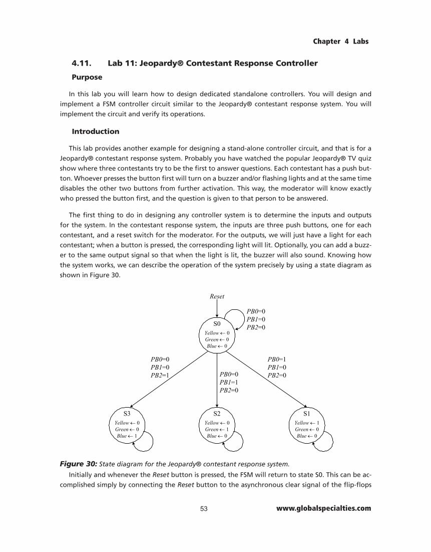
Chapter 4 Labs
www.globalspecialties.com53
4.11. Lab 11: Jeopardy® Contestant Response Controller
Purpose
In this lab you will learn how to design dedicated standalone controllers. You will design and
implement a FSM controller circuit similar to the Jeopardy® contestant response system. You will
implement the circuit and verify its operations.
Introduction
This lab provides another example for designing a stand-alone controller circuit, and that is for a
Jeopardy® contestant response system. Probably you have watched the popular Jeopardy® TV quiz
showwherethreecontestantstrytobethefirsttoanswerquestions.Eachcontestanthasapushbut-
ton.Whoeverpressesthebuttonfirstwillturnonabuzzerand/orflashinglightsandatthesametime
disables the other two buttons from further activation. This way, the moderator will know exactly
whopressedthebuttonfirst,andthequestionisgiventothatpersontobeanswered.
Thefirstthingtodoindesigninganycontrollersystemistodeterminetheinputsandoutputs
for the system. In the contestant response system, the inputs are three push buttons, one for each
contestant, and a reset switch for the moderator. For the outputs, we will just have a light for each
contestant; when a button is pressed, the corresponding light will lit. Optionally, you can add a buzz-
er to the same output signal so that when the light is lit, the buzzer will also sound. Knowing how
the system works, we can describe the operation of the system precisely by using a state diagram as
shown in Figure 30.
S0Yellow ← 0 Green ← 0 Blue ← 0
S1Yellow ← 1 Green ← 0 Blue ← 0
S2Yellow ← 0 Green ← 1 Blue ← 0
S3Yellow ← 0 Green ← 0 Blue ← 1
PB0=0PB1=0PB2=0
Reset
PB0=1PB1=0PB2=0PB0=0
PB1=1PB2=0
PB0=0PB1=0PB2=1
Figure 30: State diagram for the Jeopardy® contestant response system.
Initially and whenever the Reset button is pressed, the FSM will return to state S0. This can be ac-
complished simply by connecting the Resetbuttontotheasynchronousclearsignaloftheflip-flops

Sequential Logic Design
Global Specialties 54
to zero the state memory. This way, the Reset signal does not have to be considered as an input signal
in the FSM design, i.e., not a label on any edges in the diagram. The system starts out in state S0 and
waits for a button press, so in the diagram, there is an edge from state S0 that goes back to S0 when
there are no button presses. When there is a button pressed, the FSM will go to one of the three
states depending on which button was pressed. For example, if PB0 is pressed then the FSM will go
to state S1. In each of the three states the FSM will turn on the corresponding light and turn off the
other two lights. In state S1 the FSM will turn on the Yellow LED and turn off the other two LEDs. In
state S2 it will turn on the Green LED and in state S3 it will turn on the Blue LED. In state S0, all of the
LEDs will be off. Furthermore, after a button has been pressed and the FSM has gone to one of the
correspondingthreestatesS1,S2orS3,theFSMwillstayinthatstateindefinitelyuntilthemoderator
resets the system by pressing the Reset button. Hence the unconditional edges from each of the three
states that loop back to itself.
From this state diagram we can now derive the next-state truth table as shown in Figure 31. Hav-
ing four states, we again use a 2-bit state encoding where 00 is the encoding for state S0, 01 for S1,
10 for S2, and 11 for S3.
When the FSM is in state S0, we are waiting for only one button press. It is safe to assume that even
when two or more contestants seem to press the button at the same time, if you “zoom in” and look
at the time line in the microseconds scale, one button will always have been pressed before another.
Therefore, we should never see the combinations where two or more buttons are pressed at exactly
the same time. If this very unlikely event happens, then we will just ignore it and remain in state S0.
With this assumption, we have eliminated all of the combinations where multiple buttons are pressed
at the same time, thus we are left with only the four combinations PB2PB1PB0 = 000, 001, 010 and
100, i.e., no button pressed, only PB0 is pressed, only PB1 is pressed, and only PB2 is pressed.
In state S0, the FSM will go to one of the other three states only if one of the three button-press
combinations (001, 010, or 100) occurs. For all other combinations, the FSM will remain in state S0.
When the FSM is in state S1, S2 or S3, it will remain in that state no matter what happens further with
the three contestant push buttons. The moderator will have to press the reset key to bring the FSM
back to state S0.
Current StateQ1Q0
Next StateD1D0
PB2PB1PB0 → 000+all other combinations 001 010 100
00 = S0 00 01 10 1101 = S1 01 01 01 0110 = S2 10 10 10 1011 = S3 11 11 11 11
Figure 31: Next-state truth table for the Jeopardy® contestant response system.
In deriving the two next-state equations, one for D0 and one for D1, we look at the 1 bits in the
2-bit bit string in the table entries. Again, the right-most bit is for D0 and the left-most bit is for D1.
MaybeyoumayfinditeasiertovisualizethebitsforD0andD1ifyouseparatethenext-statetable

Chapter 4 Labs
www.globalspecialties.com55
from Figure 31 into two separate tables, one for D0 and one for D1 as shown next.
Current StateQ1Q0
Next StateD0
000 001 010 100
00 = S0 0 1 0 101 = S1 1 1 1 110 = S2 0 0 0 011 = S3 1 1 1 1
Current StateQ1Q0
Next StateD1
000 001 010 100
00 = S0 0 0 1 101 = S1 0 0 0 010 = S2 1 1 1 111 = S3 1 1 1 1
For the D0equation,therearetwo1bitsinthefirsttworows(i.e.,whenQ1 is a 0) and under the
column 001. These two ones can be covered by the AND term Q1’ PB2’ PB1’ PB0. The two 1 bits in the
samefirsttworowsbutunderthecolumn100canbecoveredbytheANDtermQ1’ PB2PB1’ PB0’.
The four 1 bits in the second row (i.e., when Q1Q0=01) and the four 1 bits in the last row (i.e., when
Q1Q0=11) can all be covered by the AND term Q0. In other words, it doesn’t matter what the other
input values are, as long as Q0 is a 1, we want D0 to also be a 1. Since these three AND terms cover all
of the 1 bits for D0, therefore, the equation for D0 is obtained by ORing these three AND terms togeth
er as follows.
D0 = Q1’ PB2’ PB1’ PB0 + Q1’ PB2PB1’ PB0’ + Q0
Proceeding in a similar manner, we get the following equation for D1.
D1 = Q0’ PB2’ PB1 PB0’ + Q0’ PB2PB1’ PB0’ + Q1
The output truth table is shown in Figure 32. The three color LEDs used for the three contestants
are driven by the three output signals, Yellow, Green and Blue. In state S0, all of them are turned off
with a 0. In state S1, only the Yellow output signal is set to a 1 to turn on the yellow LED. In state S2,
only Green is set to a 1, and in state S3, only Blue is set to a 1.
Current StateQ1Q0
Output Signals
Yellow Green Blue
00 = S0 0 0 001 = S1 1 0 010 = S2 0 1 011 = S3 0 0 1
Figure 32: Output truth table for the Jeopardy® contestant response system.
The three output equations as derived from the output truth table are shown next:
Yellow = Q1’Q0
Green = Q1Q0’
Blue = Q1Q0
The complete Jeopardy® contestant response controller circuit is shown in Figure 33.

Sequential Logic Design
Global Specialties 56
Clock
D0
Q'0
Q0
Clear
PB0
ClockReset
Clock
D1
Q'1
Q1
Clear
Yellow
Green
Blue
8
9
10
PB1PB2
8
7
6
5
5
7
Figure 33: The complete FSM circuit for the Jeopardy® contestant response system.
Experiments - Lab 11
1. Implement the Jeopardy® contestant response FSM circuit shown Figure 33. Use the two
built-inDflip-flopsonthetrainer.ConnecttheReset signal to toggle switch SW0, and connect the
three contestant push buttons to PB0, PB1 and PB2. Connect the Clock signal to the clock genera-
tor on the trainer, and set the clock speed to 20 Hz. Connect the three output signals to the cor-
responding color LEDs. Have fun playing Jeopardy! Press the Reset key (SW0) after each round to
reset the lights.
2. What happens to the response of the contestant push buttons when you set the clock speed
to 1 Hz? Why?

Chapter 4 Labs
www.globalspecialties.com57
4.12. Lab 12: Traffic Light Controller
Purpose
In this lab you will learn how to design dedicated standalone controllers. You will design and
implementaFSMcontrollercircuitforcontrollingasimpletrafficlightsystematanintersection.You
will implement the circuit and verify its operations.
Introduction
This lab provides a slightly more complex example for designing a stand-alone controller circuit,
andthatisforasimpletrafficlightsystematanintersection.Forourtrafficlightsystem,wewillhave
two sets of lights where each set consists of the red, yellow and green lights. The sequence for the
lights to turn on in both sets is shown next.
Set 1 Set 2 Time Delay State
yellow red 1 second S0
red green 3 seconds S1
red yellow 1 second S2
green red 3 seconds S3
yellow red 1 second S0
etc. etc. etc. etc.
There is a short delay for each light until it changes to the next light. The green light remains on
for 3 seconds before switching to the yellow light, and the yellow light remains on for one second
before switching to the red light.
The system also has two crosswalk push buttons (matching the two sets of lights) for people to
cross the street. When a button is pressed, we want that matching set of lights to turn red immedi-
ately if it is not already red, i.e., if that set of lights is at green, then we want it to immediately go
to yellow without completing the 3 seconds delay. If it is already at red then it should remain at red.
It will remain at red (while the other set is at green) for 3 seconds for the people to cross the street,
after which the normal cycle repeats.
ThestatediagramforourtrafficlightcontrollerisshowninFigure34.
As you may have noticed in the state diagram, there is no reference to any timing except that on
every active clock edge, the FSM will transition to the next state. If the clock frequency is very high,
then the FSM will cycle through the states so fast that you wouldn’t see the lights pausing at each
sequence. In the description, there are two situations where we want the lights to pause for 1 second,
and this can be accomplished by using a 1 Hz clock frequency, because after 1 second, the FSM will
move on to the next state and so the lights will be changed after 1 second. However, for the situations
where we want the lights to pause for 3 seconds, we can either designate three states for keeping the
same lights on for three seconds, or have only one state but use a counter to count for three times for

Sequential Logic Design
Global Specialties 58
the FSM to stay in that one state before moving on to a new state. In our design, we have used the
latter solution. A 2-bit binary counter is used to count from 0 to 3. After the count of three, the coun-
teroverflows,andtheCountOverflow bit is used to signify that it is time to move on to a new state.
On reset, the FSM will start in state S0 with Yellow1 and Red2 turned on, and the counter is reset to
zero by setting ClearCount to a 1. After 1 second, the FSM transitions to state S1 turning on Red1 and
Green2. At this point, the counter will increment at a rate of 1 second. The FSM will remain in state S1
untileitherthecounteroverflowsbyassertingtheCountOverflow bit, which means that the time is
up, or a pedestrian has pushed PB1 and so we want the light to change immediately.
States S2 and S3 are mirror images of states S0 and S1 for the other set of lights.
CountOverflow=1or PB1=1
S0ClearCount←1
Yellow1←1 Red2←1
S1
Red1←1 Green2←1
S2ClearCount←1
Red1←1 Yellow2←1
S3Green1←1 Red2←1
CountOverflow=1or PB0=1
PB0=1 then ClearCount←1
PB1=1 then ClearCount←1
Reset
Figure 34: State diagram for the traffic light controller.
The next-state table as derived from the state diagram is shown in Figure 35.
Current StateQ1Q0
Next StateD1D0
PB1,PB0,CountOverflow → 000 001 010 011 100 101 110 111
00 = S0 01 01 01 01 01 01 01 0101 = S1 01 10 01 01 10 10 01 0110 = S2 11 11 11 11 11 11 11 1111 = S3 11 00 00 00 11 11 11 11
Figure 35: Next-state table for the traffic light controller. Some of the next-state entries in the next-state table can have different values, and it is up to you,
the designer, to decide on what you want. For instance, from state S1, if PB0 and PB1 are pressed at
the same time, should the FSM stay in S1 or move on to state S2? In the table, this is the row labeled

Chapter 4 Labs
www.globalspecialties.com59
S1 and the column labeled 110. The entry in the table is 01 which is to stay in state S1, thus giving
PB0 priority. There is no reason why you can’t give PB1 priority, and thus moving to state S2 instead.
The two next-state equations as derived from the next-state table are shown next:
D0 = Q0’ + Q1’ PB0 + Q1 PB1 + Q0 PB1’ PB0’ CountOverflow’D1 = Q1 Q0’ + Q1 PB1 + Q1 PB0’ CountOverflow’ + Q0 PB1 PB0’ + Q1’ Q0 PB0’ CountOverflow
The output table is shown in Figure 36. There are two sets of Red, Yellow and Green signals for
turning on and off the corresponding LEDs, and a ClearCount signal to zero the 2-bit counter. Notice
that for the ClearCount signal, it is set to a 1 not just inside a state, but on an edge, i.e., it is depen-
dent on both the current state and on an input signal. For example, in state S1, ClearCount is set to a
1 only when PB0 is also a 1.
Current StateQ1Q0
Output Signals
Red1 Yellow1 Green1 Red2 Yellow2 Green2 ClearCount
00 = S0 0 1 0 1 0 0 101 = S1 1 0 0 0 0 1 1 if PB0=110 = S2 1 0 0 0 1 0 111 = S3 0 0 1 1 0 0 1 if PB1=1
Figure 36: Output table for the traffic light controller.
The seven output equations as derived from the output table are shown next:
Red1 = Q1 ⊕ Q0Yellow1 = Q1’ Q0’
Green1 = Q1 Q0Red2 = Q1 Q0Yellow2 = Q1 Q0’
Green2 = Q1’ Q0ClearCount = Q0’ + Q1’ Q0 PB0 + Q1 Q0 PB1
As mentioned previously, a 2-bit binary up counter is needed to support the count delay. The
ClearCountsignalwillasserttheClearinputsignaltozerothecounter,andtheCountOverflowout-
putsignalisconnectedtothecounter’sOverflowoutputbit.
ThecompletetrafficlightcontrollercircuitisshowninFigure37.

Sequential Logic Design
Global Specialties 60
Clock
D0
Q'0
Q0
Clear
PB0
ClockReset
Clock
D1
Q'1
Q1
Clear
Red1
PB1
Yellow1
Green1
Red2
ClearCount
CountOverflow
8
6
5
4
3 3
Crosswalk buttons
Set 1traffic lights
Set 2traffic lights
6
10
9
7
7
5 6
12
11
8
8Yellow2
7
4
3
3
4
7 8
12
11 LED0
SW0
LED1
LED2
LED7
LED6
Green2 LED5
2-bit BinaryUp Counter
Clear
Clock
Overflow
Figure 37: The complete traffic light controller circuit.
Experiments - Lab 12
Thefollowinggivesstepbystepinstructionstoimplementthetrafficlightcontrollercircuitas
shown in Figure 37. For ease of debugging, you should use the same component/gate number as
given in the circuit diagram.
1. Connect the 2-bit binary up counter circuit as shown next. The operation of the counter cir-
cuitwasdiscussedinLab8.Usethetwobuilt-inDflip-flops1and2onthetrainerforthecounter
memory.
Clk
D Q
Clear
Clk
D Q
Clear
VccClockClear
Overflow 3
4
21
3
4
Connect the two Clocksignalsfrombothflip-flopstotheclockgeneratoronthetrainer.TheOver-
flow output bit will be connected to the CountOverflow input signal to the FSM. The two Clear
signalstotheflip-flopsareconnectedincommon,andtheywillbeconnectedtotheClearCount
output signal from the FSM.

Chapter 4 Labs
www.globalspecialties.com61
2. Because of the limited connection points available on the trainer, we need to add some more
connection points for the state memory. Connect the state memory as shown next. Use the two
built-inDflip-flops3and4onthetrainerforthestatememory.Flip-flop3isforD1,andflip-flop
4 is for D0.
Clock
D0
Q'0
Q0
Clear
Clock
D1
Q'1
Q1
Clear
4
3 9
10
11
12
ClockResetSW0
Q1
Q1
TheQandQ’outputsoftheflip-flopsonthetrainerhaveonlyfourwireconnectionpoints,but
this controller circuit requires more than four connections to them. To overcome this restriction
on the trainer, you can either connect the Q and Q’ outputs to the breadboard to get more con-nection points, or, as shown in the diagram above, connect the Q and Q’ outputs to NOT gates 9 through 12. The outputs of these NOT gates give you an additional six connection points each, which is enough for the circuit. In the diagram, there are two vertical connection lines for each flip-flopoutputsignal.ThetwoverticallinesforoutputsignalQ1 are shown: one is directly con-nected to Q1fromflip-flop3,andthesecondisconnectedtoQ1’ through NOT gate 10 (remem-ber, inverting Q1’ will give you Q1).
ConnectthetwoClearsignalsfrombothflip-flopstosliderswitchSW0.Thisistheresetsignalforthecontroller.ConnectthetwoClocksignalsfrombothflip-flopstotheclockgeneratoronthetrainer, and set the clock speed to 1 Hz.
Thecompletetrafficlightcontrollercircuitwiththemodifiedstatememoryconnectionsisshown
in Figure 38.
3. Connect the output circuit as shown in Figure 38. LED0, LED1 and LED2 are the red, yellow andgreenLEDsforonesetofthetraffic light,andLED5,LED6andLED7aretheLEDsforthesecond set. Remember to use the connections from the output of the NOT gates from the state memory. The ClearCount output signal is connected to the Clear signal of the counter.
4. Connect the next-state circuit as shown in Figure 38. Use as much as possible the Q and Q’ connectionpointsfromthetwostatememoryflip-flops.Ifnotenough,thenusetheconnectionpoints from the NOT gates from the state memory. PB0 and PB1 are the two crosswalk push but-tons. The Overflow signal from the counter is connected to an extra NOT gate, again because more connection points are needed.

Sequential Logic Design
Global Specialties 62
Youshouldseethetrafficlightssequencethroughaccordingtoourstatediagram.Makesurethat
the two crosswalk buttons work according to our design.
Clock
D0
Q'0
Q0
Clear
PB0
ClockReset
Clock
D1
Q'1
Q1
Clear
Red1
PB1
Yellow1
Green1
Red2
ClearCount
CountOverflow
8
6
5
4
3 3
Crosswalk buttons
Set 1traffic lights
Set 2traffic lights
6
10
9
7
7
5 6
12
11
8
8Yellow2
7
4
3
3
4
7 8
12
11 LED0
SW0
LED1
LED2
LED7
LED6
9
10
11
12
Green2 LED5
2-bit BinaryUp Counter
Clear
Clock
Overflow
8
Figure 38: The complete traffic light controller circuit with modified state memory connections.

Chapter 4 Labs
www.globalspecialties.com63

