growth of copper oxide thin films for possible...
TRANSCRIPT
Chapter 4
Growth of copper oxide thin
films for possible transparent
electronic applications
4.1 Introduction
The first reported semiconductor metal oxide was cuprous oxide in
1917 by Kennard et al [230]. It was used for solid state device even
before the era of silicon devices. Several reports on copper oxides
have been published in recent years mainly because of their p-type
conductivity, making these key semiconductor materials for active ap-
plications in the field of transparent electronics [231, 232].
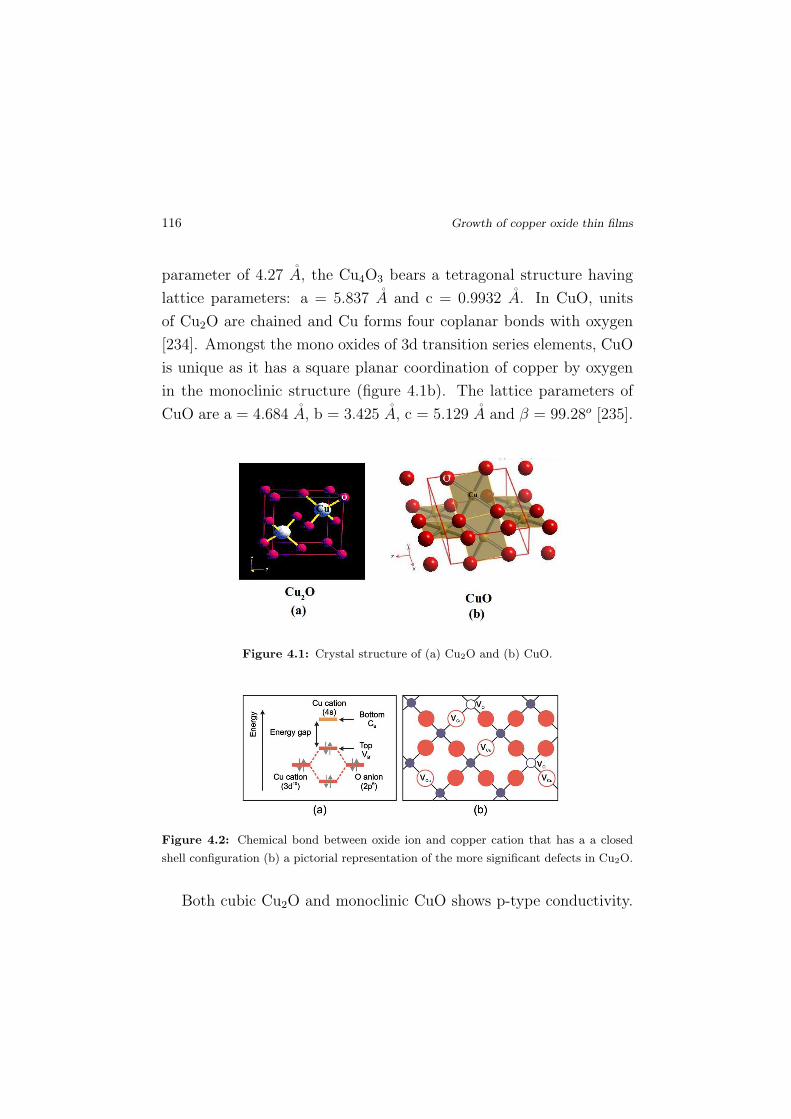
Copper forms two well known oxides: cuprite (Cu2O) and tenorite
(CuO). A metastable copper oxide, paramelaconite (Cu4O3 ), which
is an intermediate compound between the previous two, has also been
reported[233]. Cu2O forms a cubic (figure 4.1a) structure with a lattice
115
116 Growth of copper oxide thin films
parameter of 4.27 A, the Cu4O3 bears a tetragonal structure having
lattice parameters: a = 5.837 A and c = 0.9932 A. In CuO, units
of Cu2O are chained and Cu forms four coplanar bonds with oxygen
[234]. Amongst the mono oxides of 3d transition series elements, CuO
is unique as it has a square planar coordination of copper by oxygen
in the monoclinic structure (figure 4.1b). The lattice parameters of
CuO are a = 4.684 A, b = 3.425 A, c = 5.129 A and β = 99.28o [235].
Figure 4.1: Crystal structure of (a) Cu2O and (b) CuO.
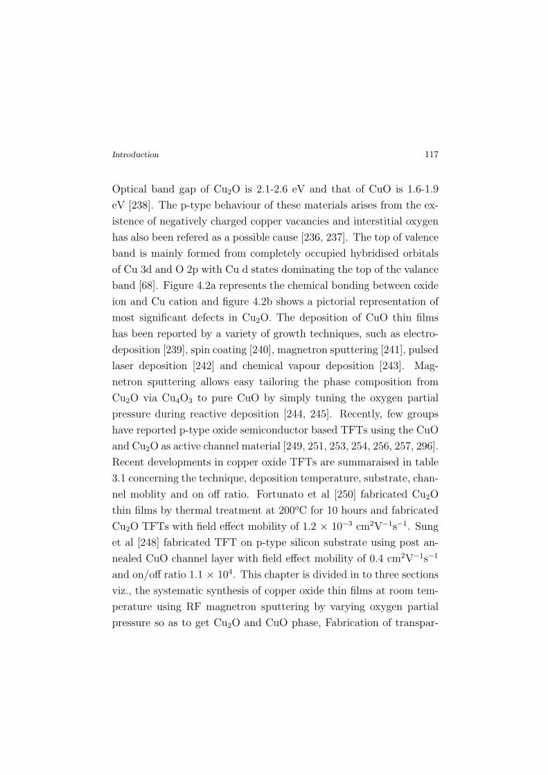
Figure 4.2: Chemical bond between oxide ion and copper cation that has a a closed
shell configuration (b) a pictorial representation of the more significant defects in Cu2O.
Both cubic Cu2O and monoclinic CuO shows p-type conductivity.
Introduction 117
Optical band gap of Cu2O is 2.1-2.6 eV and that of CuO is 1.6-1.9
eV [238]. The p-type behaviour of these materials arises from the ex-
istence of negatively charged copper vacancies and interstitial oxygen
has also been refered as a possible cause [236, 237]. The top of valence
band is mainly formed from completely occupied hybridised orbitals
of Cu 3d and O 2p with Cu d states dominating the top of the valance
band [68]. Figure 4.2a represents the chemical bonding between oxide
ion and Cu cation and figure 4.2b shows a pictorial representation of
most significant defects in Cu2O. The deposition of CuO thin films
has been reported by a variety of growth techniques, such as electro-
deposition [239], spin coating [240], magnetron sputtering [241], pulsed
laser deposition [242] and chemical vapour deposition [243]. Mag-
netron sputtering allows easy tailoring the phase composition from
Cu2O via Cu4O3 to pure CuO by simply tuning the oxygen partial
pressure during reactive deposition [244, 245]. Recently, few groups
have reported p-type oxide semiconductor based TFTs using the CuO
and Cu2O as active channel material [249, 251, 253, 254, 256, 257, 296].
Recent developments in copper oxide TFTs are summaraised in table
3.1 concerning the technique, deposition temperature, substrate, chan-
nel moblity and on off ratio. Fortunato et al [250] fabricated Cu2O
thin films by thermal treatment at 200oC for 10 hours and fabricated
Cu2O TFTs with field effect mobility of 1.2 × 10⁻³ cm2V−1s−1. Sung
et al [248] fabricated TFT on p-type silicon substrate using post an-
nealed CuO channel layer with field effect mobility of 0.4 cm2V−1s−1
and on/off ratio 1.1 × 10⁴. This chapter is divided in to three sections
viz., the systematic synthesis of copper oxide thin films at room tem-
perature using RF magnetron sputtering by varying oxygen partial
pressure so as to get Cu2O and CuO phase, Fabrication of transpar-
118 Growth of copper oxide thin films
ent flexible pn heterojunction in the structure PET/ITO/n-ZnO/p-
CuO/Au and fabrication of room temperature deposited transparent
p-type thin film transistors with Cu2O and CuO channel layers.
Intro
ductio
n119
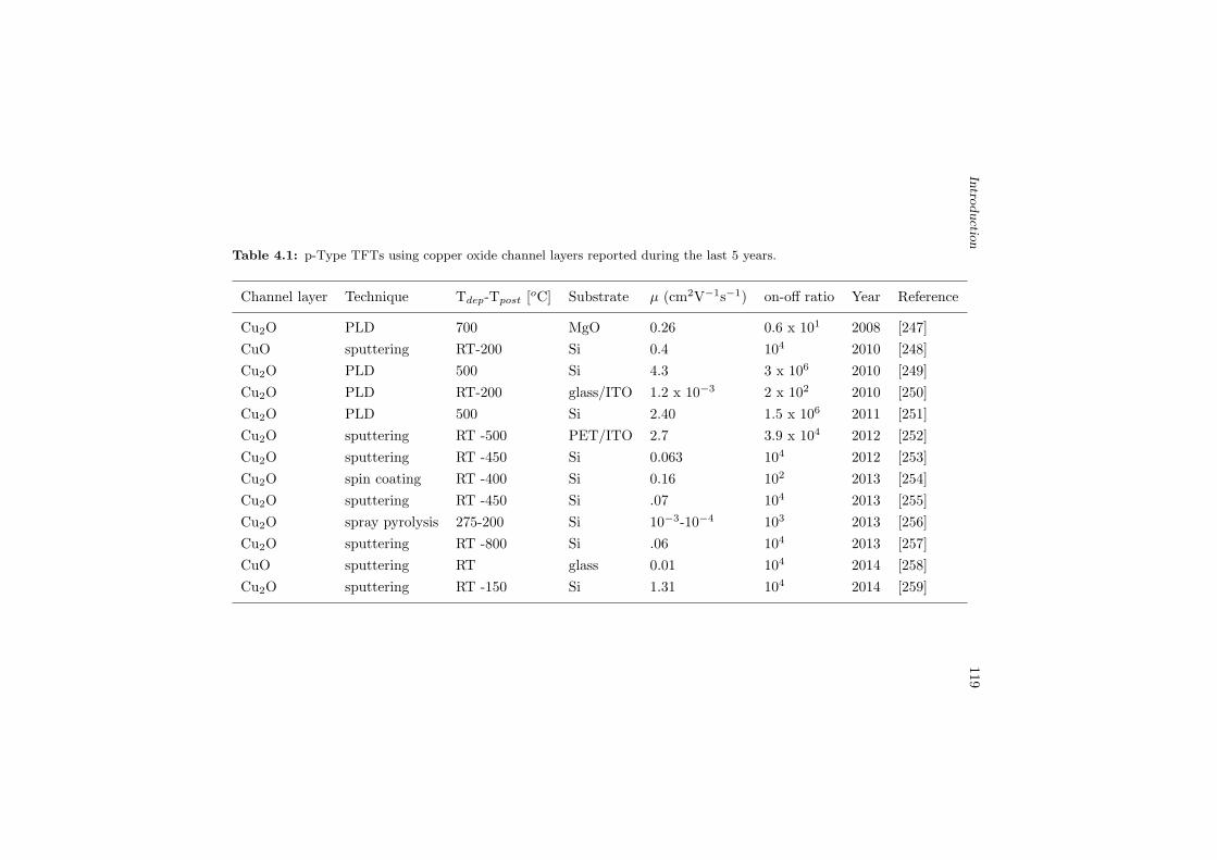
Table 4.1: p-Type TFTs using copper oxide channel layers reported during the last 5 years.
Channel layer Technique Tdep-Tpost [oC] Substrate µ (cm2V−1s−1) on-off ratio Year Reference
Cu2O PLD 700 MgO 0.26 0.6 x 101 2008 [247]
CuO sputtering RT-200 Si 0.4 104 2010 [248]
Cu2O PLD 500 Si 4.3 3 x 10⁶ 2010 [249]
Cu2O PLD RT-200 glass/ITO 1.2 x 10⁻³ 2 x 10² 2010 [250]
Cu2O PLD 500 Si 2.40 1.5 x 10⁶ 2011 [251]
Cu2O sputtering RT -500 PET/ITO 2.7 3.9 x 10⁴ 2012 [252]
Cu2O sputtering RT -450 Si 0.063 104 2012 [253]
Cu2O spin coating RT -400 Si 0.16 102 2013 [254]
Cu2O sputtering RT -450 Si .07 104 2013 [255]
Cu2O spray pyrolysis 275-200 Si 10−3-10−4 103 2013 [256]
Cu2O sputtering RT -800 Si .06 104 2013 [257]
CuO sputtering RT glass 0.01 104 2014 [258]
Cu2O sputtering RT -150 Si 1.31 104 2014 [259]
120 Growth of copper oxide thin films
4.2 Growth and characterisation of copper oxide
thin films
4.2.1 Experimental
Copper oxide thin films were deposited on glass substrates by RF
magnetron sputtering using a metallic copper (99.999% pure, 2 inch
dia) target. Depositions were carried out at room temperature in a
controlled atmosphere of oxygen and argon which favors the formation
of Cu2O or CuO phase depending on the oxygen to argon ratio in the
chamber. Base pressure of the chamber was 6×10⁻⁶ mbar. Target to
substrate distance was kept constant at 10 cm for all depositions. RF
power was fixed at 60 W and substrates were rotated at a speed of
200 o/s. Flow rate of argon to the chamber was 50 sccm for the entire
deposition process and the oxygen flow rate was varied from 0.4 sccm
to 16 sccm. The sputtering was performed for 30 minutes at different
oxygen partial pressure Opp = Po2Po2+PAr
x 100.
The structural characterization of the copper oxide thin films were
carried out by PANalytical X’Pert PRO x-ray diffractometer using Cu
Kα line (1.542512 A). Compositional analysis was carried out by x-ray
photo electron spectroscopy (XPS). The thicknesses of the thin films
were measured by a stylus profiler (Dektak 6M). Surface morphology
of the film was studied by Agilent 5500 series atomic force microscopy
(AFM) in non contact mode. Optical transmittance measurements
were performed with Jasco V-570, UV-vis-NIR spectrophotometer.
Transport properties were studied by Hall effect measurement in the
van der Pauw geometry using Ecopia, HMS-3000.
Results and discussion 121
4.2.2 Results and discussion
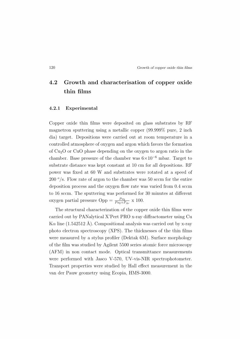
Figure 4.3: Variation of film thickness with oxygen partial pressure.
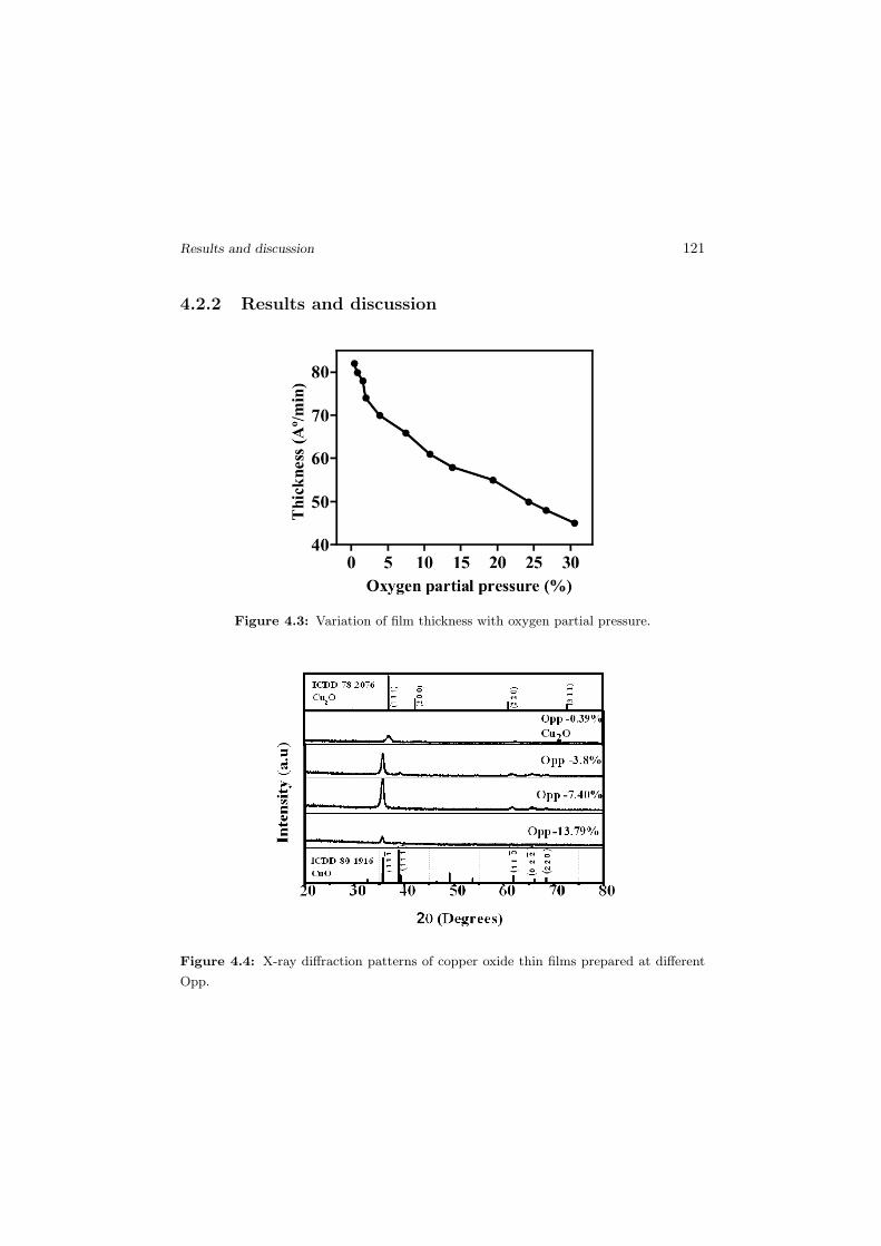
Figure 4.4: X-ray diffraction patterns of copper oxide thin films prepared at different
Opp.
122 Growth of copper oxide thin films
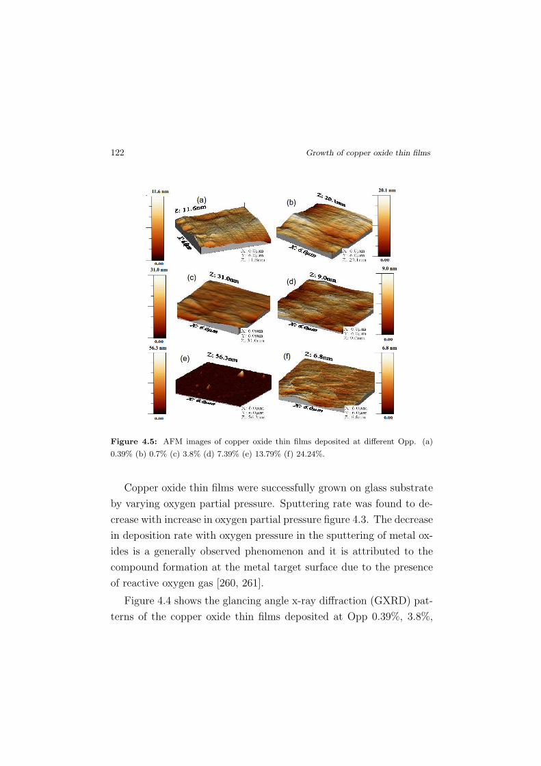
Figure 4.5: AFM images of copper oxide thin films deposited at different Opp. (a)
0.39% (b) 0.7% (c) 3.8% (d) 7.39% (e) 13.79% (f) 24.24%.
Copper oxide thin films were successfully grown on glass substrate
by varying oxygen partial pressure. Sputtering rate was found to de-
crease with increase in oxygen partial pressure figure 4.3. The decrease
in deposition rate with oxygen pressure in the sputtering of metal ox-
ides is a generally observed phenomenon and it is attributed to the
compound formation at the metal target surface due to the presence
of reactive oxygen gas [260, 261].
Figure 4.4 shows the glancing angle x-ray diffraction (GXRD) pat-
terns of the copper oxide thin films deposited at Opp 0.39%, 3.8%,
Results and discussion 123
7.4% and 13.7% respectively for 30 minutes at room temperature. It
can be seen from the figure that at Opp 0.39% Cu2O film with cubical
structure (ICDD-78-2076) is obtained and at higher Opp CuO phase
with monoclinic structure is obtained. This indicates that the oxida-
tion of Cu1+ to Cu2+ when increasing the oxygen partial pressure. All
the diffraction peaks were in line with the reported ICDD (80-1916)
data of CuO.
Surface morphology of the CuO thin films were studied by atomic
force microscopy(AFM). Figure 4.5 shows three dimensional AFM
morhology of copper thin films deposited at different oxygen partial
pressures. Rms roughness values were 1.41 nm, 2.8 nm, 2.37 nm, 1.33
nm , 1.90 nm and 0.63 nm for the copper oxide films deposited at at
0.39%, 0.7%, 3.8%, 7.4%, 13.79% and 24.24% respectively. CuO films
with smooth surface ( Opp: 7.39% and 13.79%) were used for device
fabrications.
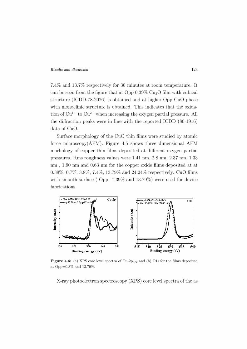
Figure 4.6: (a) XPS core level spectra of Cu-2p3/2 and (b) O1s for the films deposited
at Opp=0.3% and 13.79%.
X-ray photoelectron spectroscopy (XPS) core level spectra of the as
124 Growth of copper oxide thin films
deposited copper oxide thin films at different oxygen pressure is shown
in figure 4.6. By increasing the oxygen partial pressure the binding
energy of Cu 2p3/2 in the as-deposited films increased from 932.5 eV to
933.4 eV due to the oxidation of Cu+ to Cu2+. The binding energies
of O 1s were observed to be 530.45 eV for the as-deposited Cu2O
films and 529.95 eV for CuO films deposited at higher Opp(13.73%).
Binding energy values obtained in this experiment are similar to the
observation made by Ghijsen et al [267]. These results indicated that
copper oxide film deposited at Opp = 0.39% and Opp = 13.73% have
one main peak of Cu+, Cu2+ respectively. It is evident that higher
Opp is required for the formation of CuO phase.
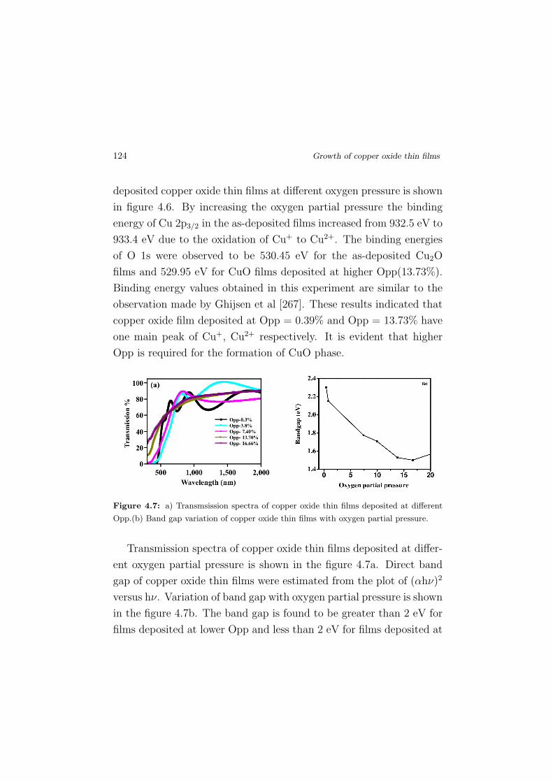
Figure 4.7: a) Transmsission spectra of copper oxide thin films deposited at different
Opp.(b) Band gap variation of copper oxide thin films with oxygen partial pressure.
Transmission spectra of copper oxide thin films deposited at differ-
ent oxygen partial pressure is shown in the figure 4.7a. Direct band
gap of copper oxide thin films were estimated from the plot of (αhν)2
versus hν. Variation of band gap with oxygen partial pressure is shown
in the figure 4.7b. The band gap is found to be greater than 2 eV for
films deposited at lower Opp and less than 2 eV for films deposited at
Results and discussion 125
higher Opp, which indicates conversion of Cu2O phase to CuO phase
as the oxygen partial pressure increases [268].
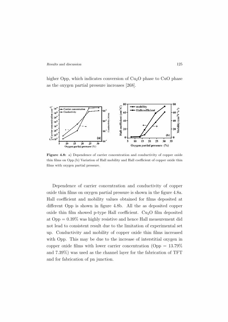
Figure 4.8: a) Dependence of carrier concentration and conductivity of copper oxide
thin films on Opp.(b) Variation of Hall mobility and Hall coefficient of copper oxide thin
films with oxygen partial pressure.
Dependence of carrier concentration and conductivity of copper
oxide thin films on oxygen partial pressure is shown in the figure 4.8a.
Hall coefficient and mobility values obtained for films deposited at
different Opp is shown in figure 4.8b. All the as deposited copper
oxide thin film showed p-type Hall coefficient. Cu2O film deposited
at Opp = 0.39% was highly resistive and hence Hall measurement did
not lead to consistent result due to the limitation of experimental set
up. Conductivity and mobility of copper oxide thin films increased
with Opp. This may be due to the increase of interstitial oxygen in
copper oxide films with lower carrier concentration (Opp = 13.79%
and 7.39%) was used as the channel layer for the fabrication of TFT
and for fabrication of pn junction.
126 Fabrication of pn heterojunction
4.3 Fabrication of pn heterojunction
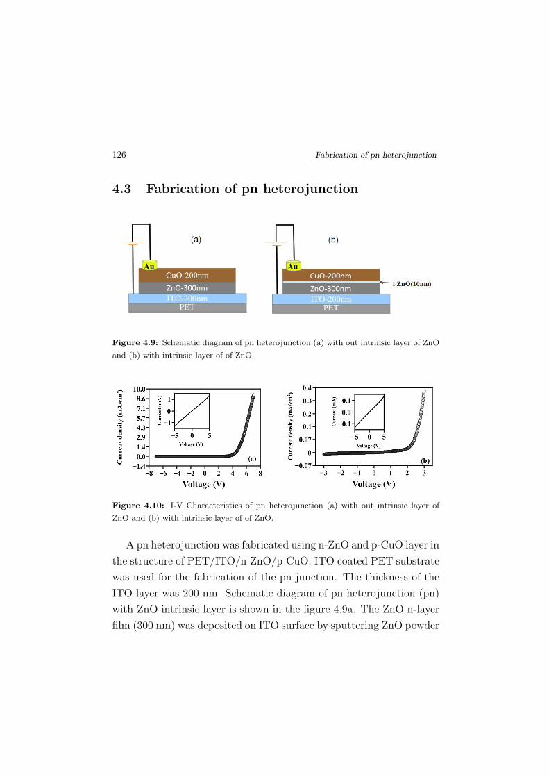
Figure 4.9: Schematic diagram of pn heterojunction (a) with out intrinsic layer of ZnO
and (b) with intrinsic layer of of ZnO.
Figure 4.10: I-V Characteristics of pn heterojunction (a) with out intrinsic layer of
ZnO and (b) with intrinsic layer of of ZnO.
A pn heterojunction was fabricated using n-ZnO and p-CuO layer in
the structure of PET/ITO/n-ZnO/p-CuO. ITO coated PET substrate
was used for the fabrication of the pn junction. The thickness of the
ITO layer was 200 nm. Schematic diagram of pn heterojunction (pn)
with ZnO intrinsic layer is shown in the figure 4.9a. The ZnO n-layer
film (300 nm) was deposited on ITO surface by sputtering ZnO powder
Results and discussion 127
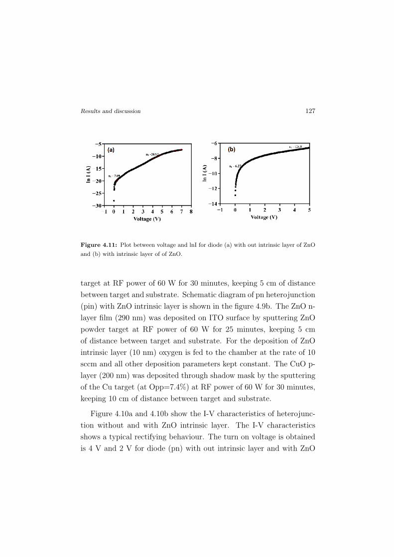
Figure 4.11: Plot between voltage and lnI for diode (a) with out intrinsic layer of ZnO
and (b) with intrinsic layer of of ZnO.
target at RF power of 60 W for 30 minutes, keeping 5 cm of distance
between target and substrate. Schematic diagram of pn heterojunction
(pin) with ZnO intrinsic layer is shown in the figure 4.9b. The ZnO n-
layer film (290 nm) was deposited on ITO surface by sputtering ZnO
powder target at RF power of 60 W for 25 minutes, keeping 5 cm
of distance between target and substrate. For the deposition of ZnO
intrinsic layer (10 nm) oxygen is fed to the chamber at the rate of 10
sccm and all other deposition parameters kept constant. The CuO p-
layer (200 nm) was deposited through shadow mask by the sputtering
of the Cu target (at Opp=7.4%) at RF power of 60 W for 30 minutes,
keeping 10 cm of distance between target and substrate.
Figure 4.10a and 4.10b show the I-V characteristics of heterojunc-
tion without and with ZnO intrinsic layer. The I-V characteristics
shows a typical rectifying behaviour. The turn on voltage is obtained
is 4 V and 2 V for diode (pn) with out intrinsic layer and with ZnO
128 Fabrication of pn heterojunction
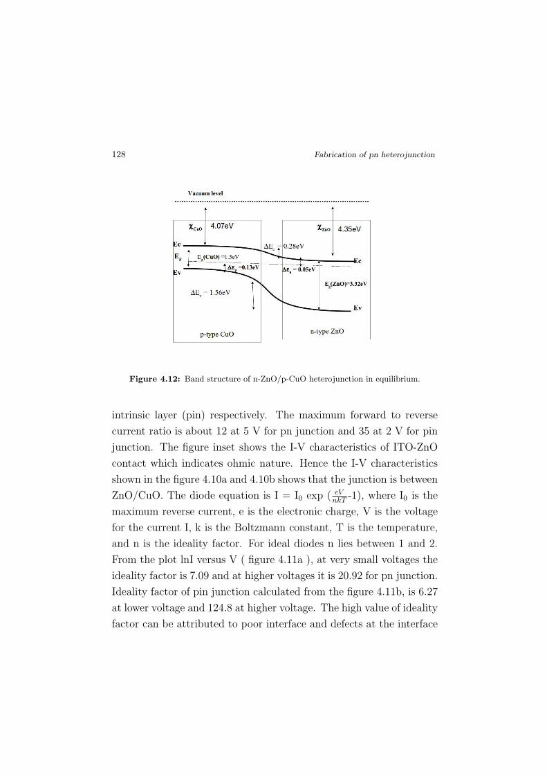
Figure 4.12: Band structure of n-ZnO/p-CuO heterojunction in equilibrium.
intrinsic layer (pin) respectively. The maximum forward to reverse
current ratio is about 12 at 5 V for pn junction and 35 at 2 V for pin
junction. The figure inset shows the I-V characteristics of ITO-ZnO
contact which indicates ohmic nature. Hence the I-V characteristics
shown in the figure 4.10a and 4.10b shows that the junction is between
ZnO/CuO. The diode equation is I = I0 exp ( eVnkT
-1), where I0 is the
maximum reverse current, e is the electronic charge, V is the voltage
for the current I, k is the Boltzmann constant, T is the temperature,
and n is the ideality factor. For ideal diodes n lies between 1 and 2.
From the plot lnI versus V ( figure 4.11a ), at very small voltages the
ideality factor is 7.09 and at higher voltages it is 20.92 for pn junction.
Ideality factor of pin junction calculated from the figure 4.11b, is 6.27
at lower voltage and 124.8 at higher voltage. The high value of ideality
factor can be attributed to poor interface and defects at the interface
Results and discussion 129
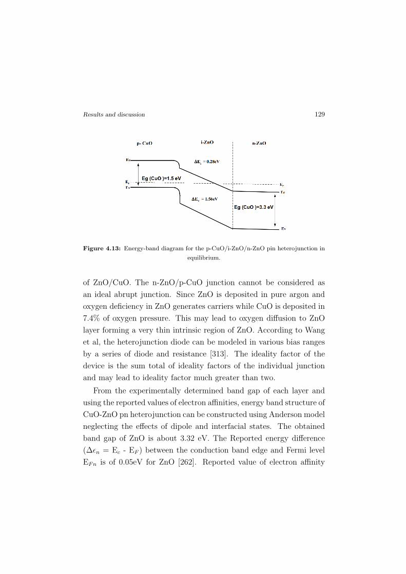
Figure 4.13: Energy-band diagram for the p-CuO/i-ZnO/n-ZnO pin heterojunction in
equilibrium.
of ZnO/CuO. The n-ZnO/p-CuO junction cannot be considered as
an ideal abrupt junction. Since ZnO is deposited in pure argon and
oxygen deficiency in ZnO generates carriers while CuO is deposited in
7.4% of oxygen pressure. This may lead to oxygen diffusion to ZnO
layer forming a very thin intrinsic region of ZnO. According to Wang
et al, the heterojunction diode can be modeled in various bias ranges
by a series of diode and resistance [313]. The ideality factor of the
device is the sum total of ideality factors of the individual junction
and may lead to ideality factor much greater than two.
From the experimentally determined band gap of each layer and
using the reported values of electron affinities, energy band structure of
CuO-ZnO pn heterojunction can be constructed using Anderson model
neglecting the effects of dipole and interfacial states. The obtained
band gap of ZnO is about 3.32 eV. The Reported energy difference
(∆ǫn = Ec - EF ) between the conduction band edge and Fermi level
EFn is of 0.05eV for ZnO [262]. Reported value of electron affinity

130 Fabrication of pn heterojunction
χe−ZnO is 4.35 eV [263]. Band gap of CuO obtained in the present
study is 1.5 eV. The energy difference ∆ǫp between the valence band
and the Fermi level EF−p, and the electron affinity (χp−CuO ) of CuO
were reported to be 0.13 eV, and 4.07 eV, respectively [264, 265]. From
these values the conduction and valence bands discontinuities ∆EC
and ∆EV [( Eg−ZnO -Eg−CuO)-∆EC ] are estimated to be 0.28 eV, and
1.56 eV, respectively. Based on these values the constructed schematic
band diagram of CuO/ZnO heterojunction obtained, is shown in figure
4.12. The energy band diagram of the synthesized CuO/ZnO pn diode
provides a first order estimation of their heterojunction under thermal
equilibrium condition.
The proposed energy-band diagram for the transparent p-CuO/i-
ZnO/In-ZnO pin heterojunction at equilibrium is shown in figure 4.13.
Intrinsic i-ZnO layer sandwiched between p-CuO and n-ZnO act as an
electron blocking layer which stabilizes particular defects and affects
Fermi-level of n-ZnO layer [266]. i-ZnO layer modulates the energy
band between n-ZnO and p-CuO smoother [270]. A thin tunneling
barrier across the pin junction is the result of large valence band off-
set. As the three materials are brought into contact electrons in the
n-ZnO are transferred to the p-CuO through the i-ZnO layer and holes
are transferred in the opposite direction until the Fermi-level is aligned
and a constant Fermi-level will be formed. Forward biasing may inject
electrons from n-ZnO layer into p-CuO layer since the energy barrier
for electrons is lower than that of holes at the heterojunction interface
[266]. When the forward bias voltage is equal to the threshold voltage,
the conduction band minimum of i-ZnO is greater than the interface
state levels [270]. The electrons from the conduction band of n-ZnO
may tunnel through the junction potential barrier into the empty in-
Results and discussion 131
terface states and then transfer in to the valence band of p-CuO to
execute a forward current [271].
4.4 Fabrication of thin film transistors
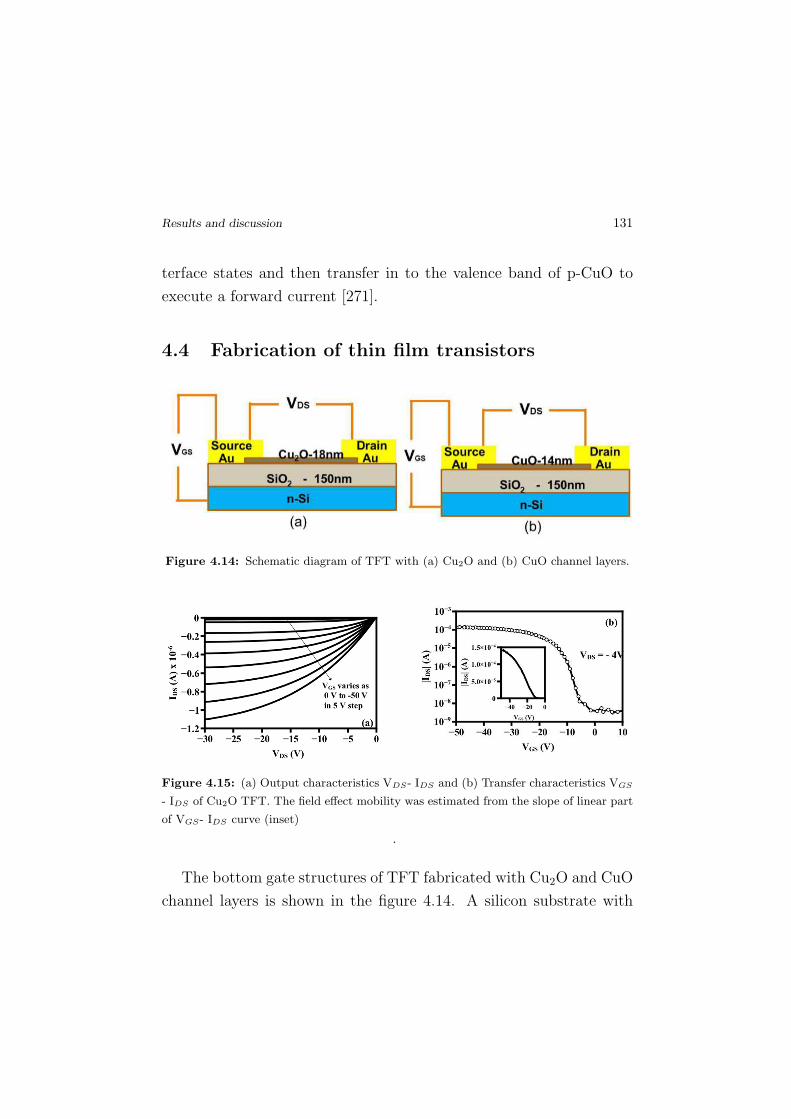
Figure 4.14: Schematic diagram of TFT with (a) Cu2O and (b) CuO channel layers.
Figure 4.15: (a) Output characteristics VDS- IDS and (b) Transfer characteristics VGS
- IDS of Cu2O TFT. The field effect mobility was estimated from the slope of linear part
of VGS- IDS curve (inset)
.
The bottom gate structures of TFT fabricated with Cu2O and CuO
channel layers is shown in the figure 4.14. A silicon substrate with
132 Fabrication of thin film transistors
thermally oxidised 200 nm thick SiO2 layer was used for TFT fab-
rication. Cu2O and CuO (14 nm) channel layers were deposited by
sputtering of copper target at 60 W for 2 minutes with Opp 0.39% and
7.39% respectively. The deposition time for the channel layer was con-
trolled knowing the sputtering rate inorder to get the desired thickness.
Sputtering rate was derived from the film thickness obtained from sty-
lus profiler for thick films. The Au source and drain electrodes were
deposited by thermal evaporation through shadow mask. The channel
width and length were 2500 µm and 60 µm, respectively.
TFT was successfully fabricated with Cu2O as channel layers. As
deposited Cu2O channel layer was annealed at 150 0C for 30 minutes.
The drain current - drain voltage (IDS-VDS) characteristics of the tran-
sistor, given in figure 4.15a, shows typical enhancement mode opera-
tion of p-channel transistor. A negative gate voltage was required to
induce the channel conduction, and the channel conductivity increased
with increase of negative gate voltage. Figure 4.15b shows the transfer
characteristics (IDS- VGS) of the fabricated transistors which give an
on-off ratio of 104. The inset graph of figure 4.15b is the same drain
current plot on a linear scale, the slope of which is used for field effect
mobility calculation. The field effect mobility extracted from the lin-
ear region slope of ID-VGS plot was 1.31 cm2V−1s−1. The threshold
voltage VT , estimated by extrapolating the straight line to the VGS
axis, was -10.35 V. The negative threshold voltage indicates the en-
hancement mode operation of the device. A maximum sub threshold
voltage swing of 2.2 V/dec obtained from the transfer curve of the
devices. Zou et al reported a mobility (4.3 cm2V−1s−1) for Cu2O TFT
fabricated using PLD at 500 0C, which is the highest mobility for a
Cu2O TFT realised so far. Mobility reported for Cu2O TFT fabricated
Results and discussion 133
using room temperature sputtering is less than 1 cm2V−1s−1 only. In
the present study high mobility of 1.31 cm2V−1s−1 were obtained for
Cu2O TFT fabricated using room temperature sputtering followed by
annealing at relatively low temperature of 150 0C. The better TFT
mobility may be due to the decrease in scattering of both ionized de-
fects and the grain boundary for Cu2O channel layer. As prepared
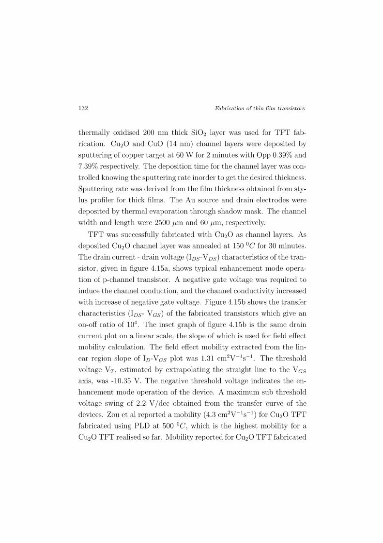
Figure 4.16: (a) Output characteristics VDS- IDS and (b) Transfer characteristics VGS
- IDS of Cu2O TFT. The field effect mobility was estimated from the slope of linear part
of VGS- IDS curve (inset)
.
CuO devices showed good transistor action without any kind of ther-
mal treatment. The drain current - drain voltage (IDS-VDS) charac-
teristics of the transistor is given in figure 4.16a. Non ideal behaviour
of the output characteristics may be due to either the series resistance
of the electrodes or due to the large leakage current [269]. Figure
4.16b shows the transfer characteristics (IDS- VGS) of the fabricated
transistors which give an on-off ratio of 103. The inset graph of figure
4.16b is the same drain current plot on a linear scale from which the
field effect mobility extracted from the slope of linear region was 1.43
× 10−2 cm2V−1s−1. The threshold voltage VT , estimated by extrap-
134 Fabrication of thin film transistors
olating the straight line to the VGS axis, was -19.08 V. A maximum
sub threshold voltage swing of 4.8 V/dec obtained from the transfer
curve of the devices.
4.4.1 Fabrication of p-channel transparent CuO thin film
transistor
Transparent electronics is an advancing science and technology field
aimed on manufacturing invisible electronic circuits. Transparent elec-
tronics came in to a reality only after the development of p-type wide
band gap oxide thin films. Transparent thin film transistors(TTFTs)
are attracting more attention since it is a key device in realising trans-
parent displays. Even though some people have reported copper based
oxide TFTs as mentioned in the literature, up to the date there is
no report on p-channel copper oxide TTFTs. In this section room
temperature deposited transparent CuO thin film transistor on glass
substrate is discussed.
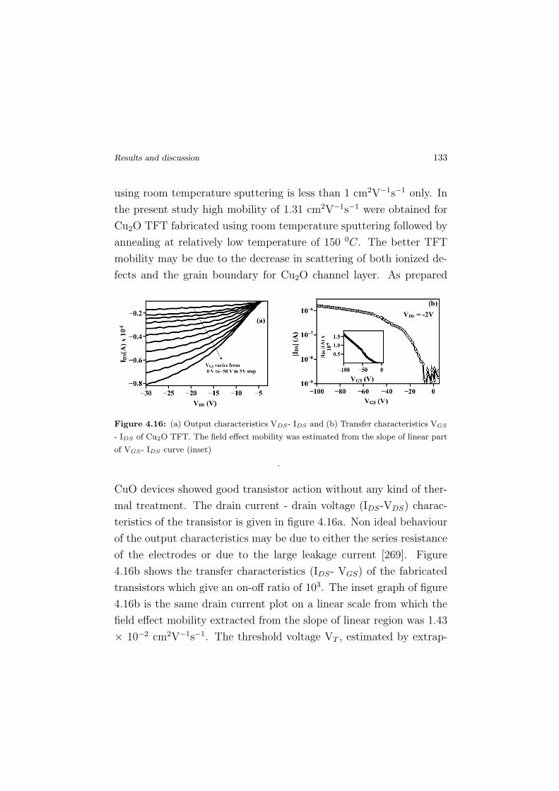
Figure 4.17: Schematic diagram of transparent TFT using p-type CuO as channel
layer.
The bottom gate structures of transparent TFT fabricated with p-

Results and discussion 135
channel CuO is shown in the figure 4.17. A glass substrate deposited
with 200nm thick layer of sputtered ITO and a 220nm thick layer of
aluminium-titanium oxide (ATO), supplied by Planar Systems Inc.,
was used for TFT fabrication. ITO electrode is a highly transparent
n-type conductor (sheet resistance 20Ω/cm2) which acts as the TFT
gate. ATO is an engineered insulator consisting of a superlattice of
alternating layers of Al2O3 and TiO2, which serves as gate insulator.
A 15 nm thick CuO channel layer was deposited by RF sputtering
using a 2 inch diameter metallic copper( 99.99% pure) target at 60 W.
Depositions were carried out at room temperature for two minutes,
in a controlled atmosphere of oxygen (8 sccm) and argon (50 sccm)
to favor the formation of CuO phase. Base pressure of the chamber
was 7 ×10⁻⁶mbar. Target substrate distance was kept at 10 cm for all
depositions. Oxygen flow percentage [Opp = ( Po2Po2+PAr
)× 100] to the
chamber during deposition of CuO channel layer was 13.7%. Thick-
ness of the channel layer was controlled by controlling the deposition
time knowing the sputtering rate. Sputtering rate was calculated by
measuring the thickness of the film using stylus profiler and duration
of sputtering. By knowing the deposition rate we could control the
channel thickness by controlling the deposition time. The TFT cross
sectional analysis was performed using Carl Zeiss Neon 40 FIB/SEM.
From the cross sectional SEM (figure 4.18b), the individual layers of
the device can be distinguished and the thickness of the CuO layer
was found to be 12 nm which is good agreement with the thickness es-
timated from rate of deposition. The Au source and drain electrodes
were deposited by thermal evaporation through shadow mask. The
channel width and length were 2500 µm and 60 µm, respectively.
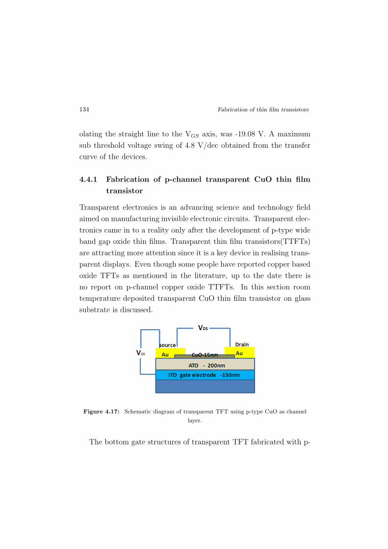
Transmission spectra of CuO channel layer (12 nm) and the device
136 Fabrication of thin film transistors
400 600 800 10000
20
40
60
80
100CuO film Device
T
rans
mis
sion
%
Wavelength (nm)
(a)
Figure 4.18: (a) Transmission spectra of CuO thin film (15nm) and the device. Inset
figure is the photograph of the device (b) cross sectional SEM image of CuO TFT.
along with the photographs of transparent devices is also shown in
the figure 4.18a. TFT shows average transmission greater than 70%
in the visible region. The devices are completely transparent to visible
light which is confirmed by the back ground images visible though the
device structure.
As prepared CuO devices showed good transistor action without
any kind of thermal treatment. The drain current - drain voltage
(IDS-VDS) characteristics of the transistor, given in figure 4.19a, shows
typical enhancement mode operation of p-channel transistor. A nega-
tive gate voltage was required to induce the channel conduction, and
the channel conductivity increased with increase of negative gate volt-
age. Non ideal behaviour of the output characteristics may be due
to either the series resistance of the electrodes or due to the large
leakage current [269]. Figure 4.19b shows the transfer characteristics
(IDS- VGS) of the fabricated transistors which give an on-off ratio of
Conclusion 137
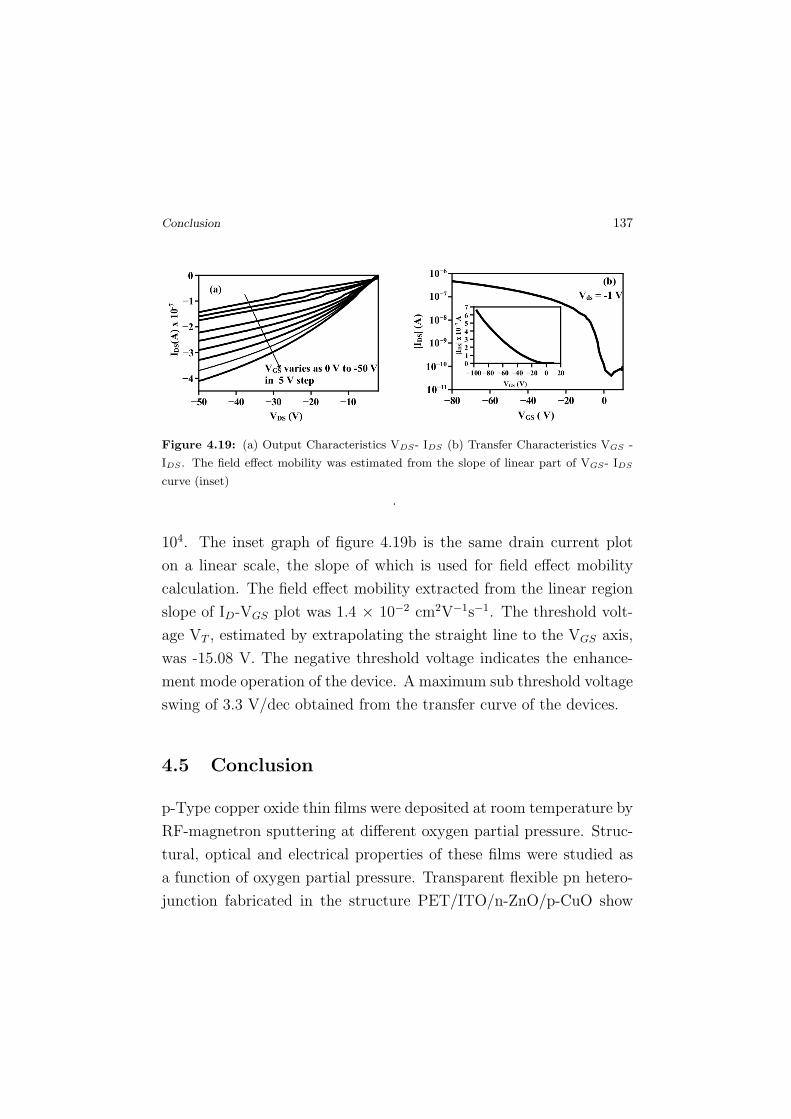
Figure 4.19: (a) Output Characteristics VDS- IDS (b) Transfer Characteristics VGS -
IDS . The field effect mobility was estimated from the slope of linear part of VGS- IDS
curve (inset)
.
104. The inset graph of figure 4.19b is the same drain current plot
on a linear scale, the slope of which is used for field effect mobility
calculation. The field effect mobility extracted from the linear region
slope of ID-VGS plot was 1.4 × 10⁻² cm2V−1s−1. The threshold volt-
age VT , estimated by extrapolating the straight line to the VGS axis,
was -15.08 V. The negative threshold voltage indicates the enhance-
ment mode operation of the device. A maximum sub threshold voltage
swing of 3.3 V/dec obtained from the transfer curve of the devices.
4.5 Conclusion
p-Type copper oxide thin films were deposited at room temperature by
RF-magnetron sputtering at different oxygen partial pressure. Struc-
tural, optical and electrical properties of these films were studied as
a function of oxygen partial pressure. Transparent flexible pn hetero-
junction fabricated in the structure PET/ITO/n-ZnO/p-CuO show

138 Fabrication of thin film transistors
rectifying behaviour. Transparent p-type TFTs with CuO channel
layer were fabricated at room temperature. From the XRD and XPS
data, it was confirmed the Cu2O and CuO phase. Band gap of the
Cu2O and CuO channel layer were 2.1 eV and 1.50 eV respectively
which is relatively low as compared to n-type TCOs. Band gap of
copper oxide films could be enhanced by doping with elements like
boron, chromium etc, which effectively reduces the dimension of cross
linking of Cu ions. The bottom gate structured p-channel CuO TFTs
exhibited an on/off ratio of 104 and the field-effect mobility of 0.01
cm2 V−1s−1. TFT fabricated on Si substrate with Cu2O channel layer
exhibited an on/off ratio 104 and field effect mobility 1.31 cm2V−1s−1
which was the highest mobility obtained so far for a copper oxide TFT
fabricated using room temperature RF magnetron sputtering followed
by post deposition annealing at relatively low temperature of 150 oC in
air. Lithographically pattered source and drain may give better mobil-
ity for a TFT as compared to the shadow mask. The low temperature
process along with the better electrical performance and transparency
of the devices at this stage will contribute for the development of p-
type oxide-based devices and allowing their use in flexible, low cost
and transparent electronic circuits.