graphene and zno nanostructures for nano- optoelectronic...
TRANSCRIPT
Linköping Studies in Science and Technology Dissertations, No. 1458
Graphene and ZnO Nanostructures for Nano- Optoelectronic & Biosensing
Applications
Kamran ul Hasan
Department of Science and Technology Linköpings University, SE-601 74 Norrköping, Sweden
Norrköping 2012
Graphene and ZnO Nanostructures for Nano- Optoelectronic & Biosensing Applications
A dissertation submitted to ITN, Department of Science and Technology, Linköping University, for the degree of Doctor of Technology.
ISBN: 978-91-7519-869-9 ISSN: 0345-7524
Copyright , 2012, Kamran ul Hasan, unless otherwise noted. Linköping University Department of Science and Technology SE-601 74 Norrköping Sweden Printed by LiU-Tryck, Linköping 2012.
Abstract i ___________________________________________________________________________________________________
Abstract
There has been a remarkable excitement in graphene research since the famous discovery in 2004 by isolating a monolayer with the help of scotch tape. Graphene, merely a single layer of carbon atoms, is progressively making inroads into a wide range of applications, from ballistic electronics to biosensors to flexible/transparent displays. Graphene is a matchless material that is strong, light, transparent, and an excellent conductor of heat and electricity. On the other hand, zinc oxide (ZnO) is a wide band semiconductor that demonstrates excellent electrical, optical, catalytic and sensing properties and has numerous applications in various fields. ZnO is a natural n-type semiconductor due to the presence of intrinsic defects such as Zn interstitials and O vacancies that also contribute strongly to optical emissions in the visible region. The amalgamation of the exceptional properties of graphene with good semiconducting properties of ZnO can pave the way towards the realization of future devices (LED, biosensors, photovoltaics etc.). In this thesis, graphene nanosheets and zinc oxide (ZnO) nanostructures have been successfully synthesized by using chemical vapor deposition (CVD), vapor liquid solid (VLS) or wet chemistry routines. These nanostructures were used to fabricate nano and optoelectronic devices, including field effect transistors (FETs), light emitting diodes (LEDs), UV detectors and biosensors. Both nanomaterial’s properties and performances of the devices have been characterized and reported.

Populärvetenskaplig sammanfattning iii ___________________________________________________________________________________________________
Populärvetenskaplig sammanfattning
Det har varit en anmärkningsvärd uppståndelse kring grafenforskningen sedan den berömda upptäckten år 2004 där man isolerade ett monoskikt med hjälp av tejp. Grafen, ett enda lager av kolatomer, gör gradvis inbrytningar i ett brett spektrum av tillämpningar, allt från ballistisk elektronik för biosensorer till flexibla och transparent displayer. Grafen är ett enastående material som är starkt, lätt, transparent, och en utmärkt ledare av värme och elektricitet. Zinkoxid (ZnO) är en halvledare med stort bandgap som har utmärkta elektriska, optiska, katalytiska och avkänningsegenskaper och har därmed en mängd tillämpningar inom diverse områden. ZnO är en naturlig n-typ halvledaren på grund av närvaron av inneboende defekter, som Zn-interstitialer och O-vakanser vilka även bidrar starkt till den optiska emissionen i det synliga området. Sammanslagningen av de exceptionella egenskaperna hos grafen med de goda halvledande egenskaper hos ZnO kan bana väg för förverkligandet av framtida komponenter (LED, biosensorer, solceller etc.). I denna avhandling har nanoskikt av grafen och zinkoxid (ZnO) nanostrukturer framgångsrikt syntetiserats genom chemical vapor deposition (CVD), vapor liquid solid (VLS) och våtkemiska processer. Dessa nanostrukturer har använts för att tillverka nano-optoelektroniska komponenter som fälteffekttransistorer (FET), lysdioder (LED), UV-detektorer och biosensorer. Både egenskaper hos nanomaterialet och prestanda för komponenterna karakteriserats och rapporterats.


Acknowledgements v ___________________________________________________________________________________________________
Acknowledgements
April 26, 2012 (08:30 AM)
I approach to the conclusion of my PhD thesis. For past four years, I had wondered what this day would bring: Exhilaration or Exhaustion? Yet as I reach close to the finish line, I feel a special bond with my work. I have already started missing my lab and workplace. I have established an affiliation with science that will last for the rest of my life. I thank Allah Almighty for providing me with the opportunity and the spirit to reach this goal.
This thesis came up in effort of years since I came to the Linköping University. By that time, I have worked with a great number of people whose contribution in assorted ways deserved special mention. It is a pleasure to convey my gratitude to them all in my sincere acknowledgment.
I am heartily thankful to my supervisor, Prof. Magnus Willander, whose encouragement, guidance and support from the initial to the final level enabled me to surpass all the obstacles in the completion of this research work. He encouraged me to not only grow as an experimentalist but also as an instructor and an independent thinker.
I am deeply grateful to my co-supervisor, associate Prof. Omer Nour, for his detailed and constructive comments, and for his important support throughout this work.
I would like to thank the research administrators Ann-Christin Norén and Sophie Lindesvik for all the administrative help. I thank Lars Gustavsson for his readiness in finding solutions for all our problems in the lab. I am also grateful to the Linköping University administration for the unperturbed support during my difficult moments.
I owe my sincere gratitude to Björn Magnusson from Norstel, for his valuable advice and friendly help. His extensive discussions around my work and interesting explorations in operations have been very helpful for this study.
I warmly thank all personnel at Acreo, especially Annelie Eveborn, Bengt Råsander, Anurak Sawatdee and Darius Jakonis for all the help in the lab and valuable discussions. Particularly, I thank Mats O. Sandberg for his creative input and valuable support during this work.
I am also grateful to Amir Karim and Jawad ul Hassan for their friendly help, support and guidance.
I would like to thank my friends Zia and Gul for helping me through the difficult times, and for all the emotional support, camaraderie, entertainment

vi Acknowledgements ___________________________________________________________________________________________________
and care they provided. I am indebted to all my friends and colleagues for providing a stimulating and fun environment. I am especially grateful to Asif, Ahmed, Artsem, Olga, Jiang, Amanda, Usman, Taras, Naveed, Kishwar, Israr, Sadaf, Saima, Hui, Henrik, Loig, Mahziar, Ghazwan Al-Haji, Riaz and Alim.
In addition, I would like to thank all my teachers during my undergraduate/graduate years, who instilled me with a love of science, especially Prof. Mujahid Kamran, Prof. Arshad Bhatti, Prof. Amir Azam Khan, Prof. Hassan Sayyad, Prof. Jameel-Un Nabi and Prof. Khasan Karimov. Special thanks to Prof. N. M. Butt and Waqar A. Butt, who made sure that my experience at the Lindau Meeting with Nobel Laureates, was very fruitful and who provided me with enthralling inspiration and guidance.
I wish to thank my entire family for providing a loving support for me. My brothers, my brother-in-law and my sister all were particularly supportive. Most importantly, I wish to thank my affectionate parents. They raised me, supported me, taught me, and loved me. I give my parents a lot of credit for my success.
I owe my loving thanks to my wife Yousra and my son Saifan. Without their presence, encouragement and understanding it would have been impossible for me to complete this work. Thank you Yousra, for supporting and taking good care of me during all this time.
Kamran ul Hasan
Norrköping, April 2012.

viii List of publications ___________________________________________________________________________________________________
List of Publications
Papers included in this thesis:
1. Polycation stabilization of graphene suspensions K. ul Hasan, M. Sandberg, O. Nur, and M. Willander, Nanoscale Research Letters, vol. 6, p. 493, 2011.
2. Controlled growth of ZnO nanowires on graphene surface Kamran ul Hasan, Björn Magnusson, Erik Janzén, Omer Nur, Magnus Willander, (submitted).
3. Recent progress on growth and device development of ZnO and CuO nanostructures and graphene nanosheets
M. Willander, K. ul Hasan, O. Nur, A. Zainelabdin, S. Zaman, and G. Amin, Journal of Materials Chemistry, vol. 22, 2012.
4. Structural characterization and biocompatible applications of graphene nanosheets for miniaturization of potentiometric cholesterol biosensor
M. Q. Israr, K. ul Hasan, J. R. Sadaf, I. Engquist, O. Nur, M. Willander, and B. Danielsson, J Biosens Bioelectron 2, vol. 2, 2011.
5. Needle-type glucose sensor based on functionalized graphene K. ul Hasan, M. H. Asif, O. Nur and M. Willander, J Biosens Bioelectron 2, vol. 3, 2012.
6. Graphene-based biosensor for intracellular glucose measurements K. ul Hasan, M.H. Asif, Mats O. Sandberg, O. Nur, M. Willander, Siri Fagerholm, Peter Strålfors, (submitted).
7. Single nanowire-based UV photodetectors for fast switching K. ul Hasan, N. H. Alvi, J. Lu, O. Nur, and M. Willander, Nanoscale Research Letters, vol. 6, p. 348, 2011.
8. Screen printed ZnO UV photoconductive sensor on pencil drawn circuitry over paper
Kamran ul Hasan, Omer Nur, and Magnus Willander, (Accepted for publication in Applied Physics Letters).
9. Electro-optical and cathodoluminescence properties of low temperature grown ZnO nanorods/p-GaN white light emitting diodes
S. Kishwar, K. ul Hasan, G. Tzamalis, O. Nur, M. Willander, H. S. Kwack, and D. L. S. Dang, physica status solidi (a), vol. 207, pp. 67-72, 2009.
List of publications ix ___________________________________________________________________________________________________
10. ZnO/ polyfluorene hybrid LED on an efficient hole transport layer of
graphene oxide and transparent graphene electrode Kamran ul Hasan, Mats O. Sandberg, Omer Nur, Magnus Willander, (submitted). Related Work Not Included in the thesis S. Kishwar, K. ul Hasan, N. H. Alvi, P. Klason, O. Nur, and M. Willander,
"A comparative study of the electrodeposition and the aqueous chemical growth techniques for the utilization of ZnO nanorods on p-GaN for white light emitting diodes," Superlattices and Microstructures, vol. 49, pp. 32-42, 2010.
N. Alvi, K. ul Hasan, O. Nur, and M. Willander, "The origin of the red emission in n-ZnO nanotubes/p-GaN white light emitting diodes," Nanoscale Research Letters, vol. 6, p. 130, 2011.
N. H. Alvi, K. ul Hasan, O. Nur, and M. Willander, "The effect of post-growth annealing on the colour properties of n-ZnO nanorods/p-GaN white LEDs," Lighting Research and Technology, vol. 43, pp. 331-336, September 1, 2011.
K. ul Hasan, N. H. Alvi, U. A. Shah, Jun Lu, O. Nur, and M. Willander, “Single ZnO nanowire biosensor for detection of glucose interactions,” manuscript.
Conferences K. ul Hasan, Jun Lu, O. Nur, and M. Willander, “Zinc Oxide Single
Nanowire UV Photodetector,” EPS 2012, Montreal, Canada. K. ul Hasan, O. Nur, and M. Willander, “Zinc Oxide Flexible
Photoconductive UV Sensors,” Energy Materials and Nanotechnology, EMN 2012, Orlando, USA.
Book Chapter Zinc Oxide nanostructures, growth and applications, by Pan Stanford
Publishing, Chapter 6 “ZnO devices on nonconventional substrates”, in press (2012).


List of abbreviations xi ___________________________________________________________________________________________________
List of Abbreviations
ACG Aqueous chemical growth AFM Atomic force microscopy BLG Bilayer grapheneCNT Carbon nanotube CVD Chemical vapor depositionDCE DichloroethaneDI Deionized DLE Deep level emissionDMF DimethylformamideDOS Density of states DWNT Double walled carbon nanotubesE-beam Electron beamEL Electroluminescence FET Field effect transistorFIB Focused ion beamFWHM Full width half maximum FTIR Fourier transform infrared spectroscopy GNR Graphene nanoribbonGO Graphene oxide HMT HexamethylenetramineHTCVD High temperature chemical vapor deposition IR Infrared LED Light emitting diodeNMP N-methylpyrrolidoneNW Nanowire PBS Phosphate based solutionPECVD Plasma enhanced chemical vapor deposition PL Photoluminescence PQ PolyquaterniumRIE Reactive ion etchingSAED Selected area electron diffraction Sccm Standard cubic centimeter per minuteSEM Scanning electron microscopeSiC Silicon carbide STP Standard temperature and pressure

xii List of abbreviations ___________________________________________________________________________________________________
SWNT Single walled carbon nanotubeTEM Transmission electron microscopeUV Ultraviolet VLS Vapor liquid solidWLED White light emitting diodeXPS X-ray photoelectron spectroscopy XRD X-ray diffractionZnO Zinc Oxide

Contents xiii ___________________________________________________________________________________________________
Contents
Abstract ........................................................................................................................ i
Populärvetenskaplig sammanfattning .................................................... iii
Acknowledgements ............................................................................................... v
List of Publications ............................................................................................. viii
List of Abbreviations ............................................................................................ xi
INTRODUCTION ......................................................................................................... 1
1.1 Background and motivation ............................................................................ 1
1.2 Research overview .......................................................................................... 3
1.3 Goal ................................................................................................................. 3
BACKGROUND AND LITERATURE SURVEY ..................................................... 5
2.1 Graphene ......................................................................................................... 5
2.1.1 Crystal Structure ......................................................................................... 6
2.1.2 Electronic Structure .................................................................................... 9
2.1.3 Optical properties ...................................................................................... 16
2.1.4 Vibrational properties ............................................................................... 17
2.1.5 Mechanical properties ............................................................................... 17
2.2 Graphyne: A competition for graphene ........................................................ 18
2.3 Properties of Zinc oxide ................................................................................ 20
2.3.1 Crystal structure ........................................................................................ 20
2.3.2 Electronic structure ................................................................................... 22
2.3.3 Optical properties ...................................................................................... 23
2.3.4 Mechanical and piezoelectric properties .................................................. 24
2.4 Summary ....................................................................................................... 26
Growth and processing................................................................................................ 29
3.1 Substrate preparation ..................................................................................... 29
3.2 Graphene synthesis ....................................................................................... 29
3.2.1 Graphene by solution based techniques .................................................... 30
3.2.2 Graphene preparation on SiC by sublimation ........................................... 32
3.3 Growth of ZnO nanostructures ..................................................................... 34
3.3.1 Aqueous chemical growth (ACG) ............................................................ 34
3.3.2 Vapor-liquid-solid method (VLS) ............................................................ 37

xiv Contents ___________________________________________________________________________________________________
3.4 Device processing .......................................................................................... 38
Experimental and characterization procedures ........................................................ 41
4.1 Scanning electron microscope (SEM) ........................................................... 41
4.2 Transmission electron microscope (TEM) .................................................... 43
4.3 Focused ion beam (FIB) ................................................................................ 43
4.4 Atomic force microscope (AFM) .................................................................. 44
4.5 Raman spectroscopy ...................................................................................... 45
4.6 X-ray diffraction (XRD) ................................................................................ 46
4.7 Photoluminescence (PL)/ electroluminescence (EL) .................................... 48
Results and Discussion ................................................................................................. 51
5.1 Synthesis, basic devices and junction study .................................................. 51
5.2 Biosensing applications ................................................................................. 58
5.3 UV detectors .................................................................................................. 62
5.4 Light emitting diodes (LEDs) ........................................................................ 64
6 Conclusions and Outlook .................................................................................... 67
6.1 Summary ........................................................................................................ 67
6.2 Future Outlook ............................................................................................... 68
References ..................................................................................................................... 69
C h a p t e r 1
INTRODUCTION
The revolutionary Feynman vision of a mystical field of nanotechnology, based on nanomachines that are built with atomic precision and control, promised great prospects. This prophecy made nanotechnology a buzzword and propelled a global nanotechnology race. At present, nanostructured materials are seen as the essential building blocks of the next generation electronic industries. Their unique physical and chemical properties at the nanoscale encourage invention of novel devices made from nano-circuits and nanomachines, attracting immense investments. Since the US National Nanotechnology Initiative was announced in 2000, almost every developed and developing economy is currently spending an average $10 billion per year on nanotechnology research and development. It is estimated that nearly a quarter of a trillion dollars will have been invested into nanotechnology by 2015 [1], making nanotechnology a big success.
1.1 Background and motivation
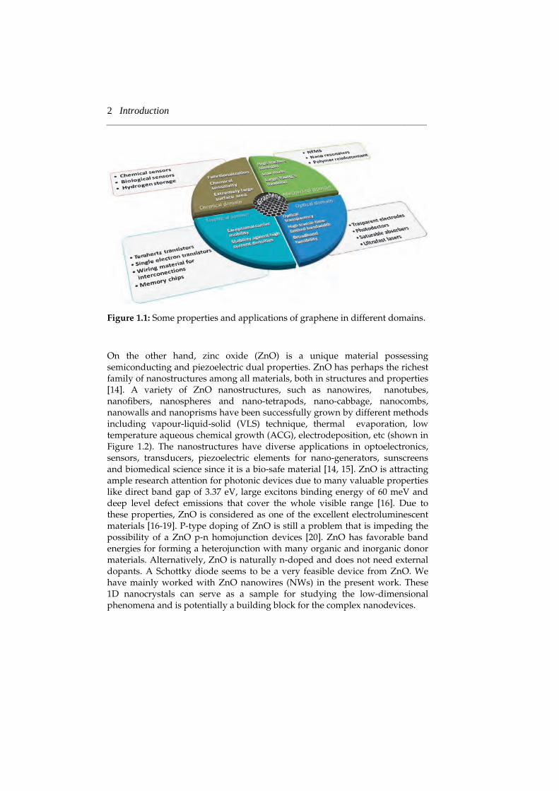
The discovery of new materials and diverse structures has been the beauty of nanotechnology over the years. With every new material come new opportunities, bringing exceptionally exciting and rewarding eras of scientific and technological research. The recent discovery of graphene [2], a perfect two-dimensional (2D) honeycomb network of carbon, has brought us on the verge of such an era. Graphene has drawn remarkable attention since its discovery in 2004, not only in the field of basic research but also in technological applications due to its unique physicochemical dimensions, high sensitivity, extremely large surface area (2630 m2 g-1), high optical transmittance (
97.7%), excellent mechanical (fracture strength, 125 GPa), thermal (thermal conductivity ~5000 W m-1 K-1) and electrical properties (carrier mobility~200 000 cm2 V-1s-1) [3-10]. The graphene gold rush [11] (so to say) began as soon as it was experimentally confirmed that its charge carriers were certainly massless Dirac fermions [12, 13]. This “wonder material” won 2010 Nobel Prize in physics and has been instigated in many applications, as illustrated in Figure 1.1. One objective of this dissertation is the synthesis of cheap solution processed graphene film and its application in optoelectronic devices such as ZnO based light emitting diodes (LEDs).
2 Introduction ___________________________________________________________________________________________________
Figure 1.1: Some properties and applications of graphene in different domains.
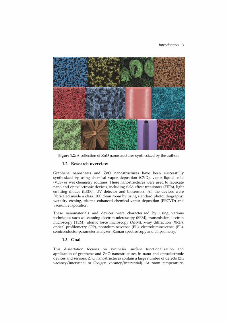
On the other hand, zinc oxide (ZnO) is a unique material possessing semiconducting and piezoelectric dual properties. ZnO has perhaps the richest family of nanostructures among all materials, both in structures and properties [14]. A variety of ZnO nanostructures, such as nanowires, nanotubes, nanofibers, nanospheres and nano-tetrapods, nano-cabbage, nanocombs, nanowalls and nanoprisms have been successfully grown by different methods including vapour-liquid-solid (VLS) technique, thermal evaporation, low temperature aqueous chemical growth (ACG), electrodeposition, etc (shown in Figure 1.2). The nanostructures have diverse applications in optoelectronics, sensors, transducers, piezoelectric elements for nano-generators, sunscreens and biomedical science since it is a bio-safe material [14, 15]. ZnO is attracting ample research attention for photonic devices due to many valuable properties like direct band gap of 3.37 eV, large excitons binding energy of 60 meV and deep level defect emissions that cover the whole visible range [16]. Due to these properties, ZnO is considered as one of the excellent electroluminescent materials [16-19]. P-type doping of ZnO is still a problem that is impeding the possibility of a ZnO p-n homojunction devices [20]. ZnO has favorable band energies for forming a heterojunction with many organic and inorganic donor materials. Alternatively, ZnO is naturally n-doped and does not need external dopants. A Schottky diode seems to be a very feasible device from ZnO. We have mainly worked with ZnO nanowires (NWs) in the present work. These 1D nanocrystals can serve as a sample for studying the low-dimensional phenomena and is potentially a building block for the complex nanodevices.
Introduction 3 ___________________________________________________________________________________________________
Figure 1.2: A collection of ZnO nanostructures synthesized by the author.
1.2 Research overview
Graphene nanosheets and ZnO nanostructures have been successfully synthesized by using chemical vapor deposition (CVD), vapor liquid solid (VLS) or wet chemistry routines. These nanostructures were used to fabricate nano and optoelectronic devices, including field effect transistors (FETs), light emitting diodes (LEDs), UV detector and biosensors. All the devices were fabricated inside a class 1000 clean room by using standard photolithography, wet/dry etching, plasma enhanced chemical vapor deposition (PECVD) and vacuum evaporation.
These nanomaterials and devices were characterized by using various techniques such as scanning electron microscopy (SEM), transmission electron microscopy (TEM), atomic force microscopy (AFM), x-ray diffraction (XRD), optical profilometry (OP), photoluminescence (PL), electroluminescence (EL), semiconductor parameter analyzer, Raman spectroscopy and ellipsometry.
1.3 Goal
This dissertation focuses on synthesis, surface functionalization and application of graphene and ZnO nanostructures in nano and optoelectronic devices and sensors. ZnO nanostructures contain a large number of defects (Zn vacancy/interstitial or Oxygen vacancy/interstitial). At room temperature,
4 Introduction ___________________________________________________________________________________________________
ZnO typically exhibits one emission peak in the UV region owing to the recombination of free excitons, and one or more peaks in the broad visible spectral range. Nevertheless, there is a possibility of enhancing or minimizing this broad defect emission. Our objective is to control and tune the surface properties according to the application requirements, e.g. white light emitting didoes (WLED) or UV detector. Moreover, the biosafety and high ionicity of ZnO seems very promising for biosensing applications.
Another goal of this dissertation is synthesis of cheap solution processed graphene and its application in optoelectronic devices such as ZnO based light emitting diodes (LEDs) and biosensors. Development of the biosensors can potentially be an interesting application of graphene in order to utilize its tremendously large surface area to volume ratio as a dominating and promising parameter. High optical transmittance, high flexibility and exceptional electrical properties make graphene a strong contender for replacing indium tin oxide (ITO) as a transparent conducting electrode in a wide range of applications such as solar cells, LEDs and electronic touch screens.
The amalgamation of the exceptional properties of graphene with good semiconducting properties of ZnO can pave the way towards the realization of future devices such as transparent, flexible electrical and photonic devices. There has been relatively very less work reported on this combination, previously. We also aim to analyze the growth mechanism of ZnO nanowires on high quality (CVD grown, epitaxial) graphene surface and the junction behavior. This combination of 1D ZnO and 2D graphene can be very important for realizing the ultimate goal of 3D assembly at the nanoscale.

C h a p t e r 2
BACKGROUND AND LITERATURE SURVEY
1 Graphene is the building block for all carbon based materials, from bulk graphite
(stacked graphene) to nanostructures such as Buckyballs (wrapped up graphene) and carbon nanotubes (rolled graphene). It was an unexpected discovery as theory prohibits existence of 2D crystals [11] but interesting properties and nature of graphene found another way around. Likewise, ZnO is a wide bandgap material possessing many interesting properties which have led to its demonstration as an alternative material to the nitride semiconductors. In this chapter, we aim to narrate properties of both these materials in a comprehensive manner.
2.1 Graphene
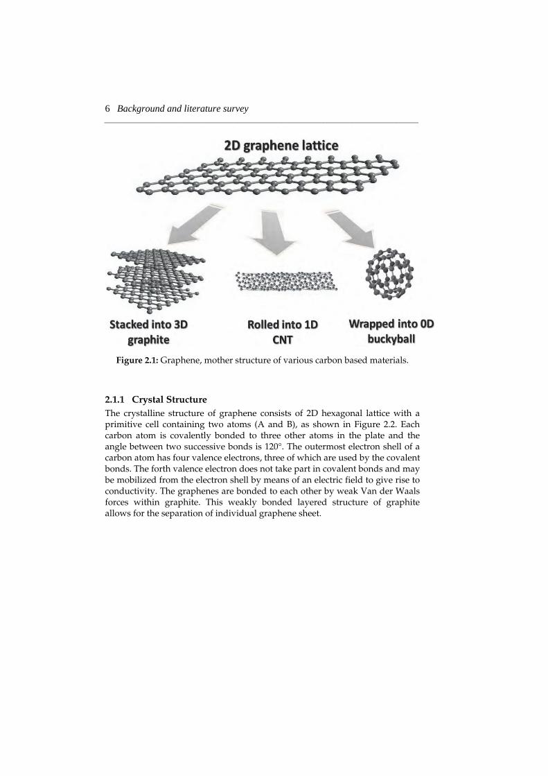
Graphene is a name given to a flat/2D monolayer of sp2 bonded carbon atoms closely packed into a honeycomb lattice with a nearest neighbor distance of 0.14 nm. Graphene can be considered as the mother structure of all the carbon based materials. It has been generally used in the approximation of the crystal structure and properties of graphite, carbon nanotubes and Buckyballs. For instance, graphite is made up of loosely stacked (ABAB type) graphene layers with an interlayer distance of 0.34 nm. This large interlayer separation, compared to the in-plane nearest neighbor distance, makes graphite a quasi 2D system.
Carbon nanotubes are usually considered as graphene layers rolled into hollow seamless cylinders and a C60 buckyball can be considered as a graphene sheet, where some hexagons are replaced by pentagons, which cause a crumbling of the sheet into a final formation of a graphene sphere or a graphene football. Graphene has been extensively studied in the last several years despite the fact that it was discovered only 6-7 years back, for the first time [2]. Andre Geim and Konstantin Novoselov won the 2010 Nobel Prize in Physics for this trailblazing discovery. This graphene gold rush has begun for good reasons, primarily owing to its several exceptional properties which are described in this section of the chapter.
6 Background and literature survey ___________________________________________________________________________________________________
Figure 2.1: Graphene, mother structure of various carbon based materials.
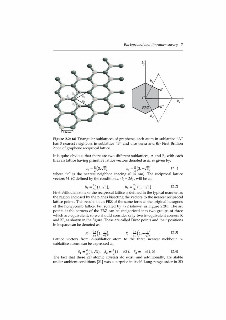
2.1.1 Crystal Structure The crystalline structure of graphene consists of 2D hexagonal lattice with a primitive cell containing two atoms (A and B), as shown in Figure 2.2. Each carbon atom is covalently bonded to three other atoms in the plate and the angle between two successive bonds is 120°. The outermost electron shell of a carbon atom has four valence electrons, three of which are used by the covalent bonds. The forth valence electron does not take part in covalent bonds and may be mobilized from the electron shell by means of an electric field to give rise to conductivity. The graphenes are bonded to each other by weak Van der Waals forces within graphite. This weakly bonded layered structure of graphite allows for the separation of individual graphene sheet.
Background and literature survey 7 ___________________________________________________________________________________________________
Figure 2.2: (a) Triangular sublattices of graphene, each atom in sublattice “A” has 3 nearest neighbors in sublattice “B” and vice versa and (b) First Brillion Zone of graphene reciprocal lattice.
It is quite obvious that there are two different sublattices, A and B, with each Bravais lattice having primitive lattice vectors denoted as a1, a2 given by;
, (2.1)
where “a” is the nearest neighbor spacing (0.14 nm). The reciprocal lattice vectors b1, b2 defined by the condition ai · bj = 2 ij , will be as;
, (2.2)
First Brillouian zone of the reciprocal lattice is defined in the typical manner, as the region enclosed by the planes bisecting the vectors to the nearest reciprocal lattice points. This results in an FBZ of the same form as the original hexagons of the honeycomb lattice, but rotated by /2 (shown in Figure 2.2b). The six points at the corners of the FBZ can be categorized into two groups of three which are equivalent, so we should consider only two in-equivalent corners K and K’, as shown in the figure. These are called Dirac points and their positions in k-space can be denoted as;
, (2.3)
Lattice vectors from A-sublattice atom to the three nearest niehbour B-sublattice atoms, can be expressed as;
, , (2.4)
The fact that these 2D atomic crystals do exist, and additionally, are stable under ambient conditions [21] was a surprise in itself. Long-range order in 2D
8 Background and literature survey ___________________________________________________________________________________________________
is not possible according to well established theory [11, 21, 22]. Thermal fluctuations should destroy the order resulting in melting the 2D lattice at any finite temperature. Actually, these 2D graphene membranes embedded in 3D space have a tendency to get crumpled. These fluctuations can be suppressed by an anharmonic coupling between bending and stretching modes, resulting in the 2D membranes, but with strong height fluctuations [23]. Experimental study of these fluctuations showed that the surface normal varies by several degrees and out-of-plane deformations are up to 1 nm [24].
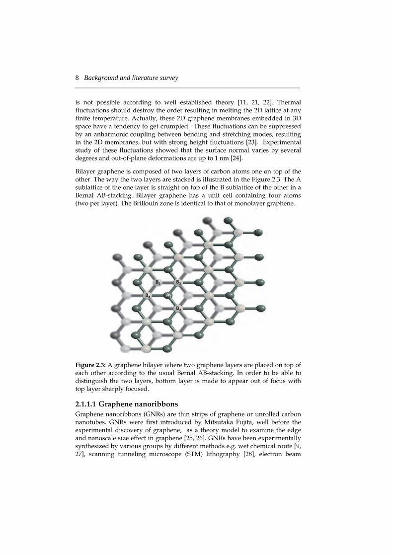
Bilayer graphene is composed of two layers of carbon atoms one on top of the other. The way the two layers are stacked is illustrated in the Figure 2.3. The A sublattice of the one layer is straight on top of the B sublattice of the other in a Bernal AB-stacking. Bilayer graphene has a unit cell containing four atoms (two per layer). The Brillouin zone is identical to that of monolayer graphene.
Figure 2.3: A graphene bilayer where two graphene layers are placed on top of each other according to the usual Bernal AB-stacking. In order to be able to distinguish the two layers, bottom layer is made to appear out of focus with top layer sharply focused.
2.1.1.1 Graphene nanoribbons Graphene nanoribbons (GNRs) are thin strips of graphene or unrolled carbon nanotubes. GNRs were first introduced by Mitsutaka Fujita, well before the experimental discovery of graphene, as a theory model to examine the edge and nanoscale size effect in graphene [25, 26]. GNRs have been experimentally synthesized by various groups by different methods e.g. wet chemical route [9, 27], scanning tunneling microscope (STM) lithography [28], electron beam
Background and literature survey 9 ___________________________________________________________________________________________________
lithography [29], etc. Recently there have been some very interesting reports on GNRs, for instance, GNRs have been synthesized encapsulated in single-walled carbon nanotubes (SWNTs) [30] and also GNRs have been twisted to form SWNTs [31].
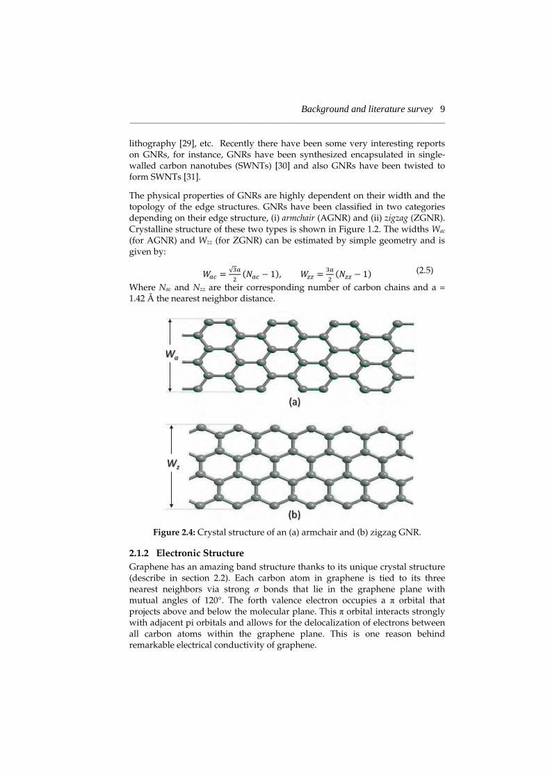
The physical properties of GNRs are highly dependent on their width and the topology of the edge structures. GNRs have been classified in two categories depending on their edge structure, (i) armchair (AGNR) and (ii) zigzag (ZGNR). Crystalline structure of these two types is shown in Figure 1.2. The widths Wac (for AGNR) and Wzz (for ZGNR) can be estimated by simple geometry and is given by:
, (2.5)
Where Nac and Nzz are their corresponding number of carbon chains and a = 1.42 Å the nearest neighbor distance.
Figure 2.4: Crystal structure of an (a) armchair and (b) zigzag GNR.
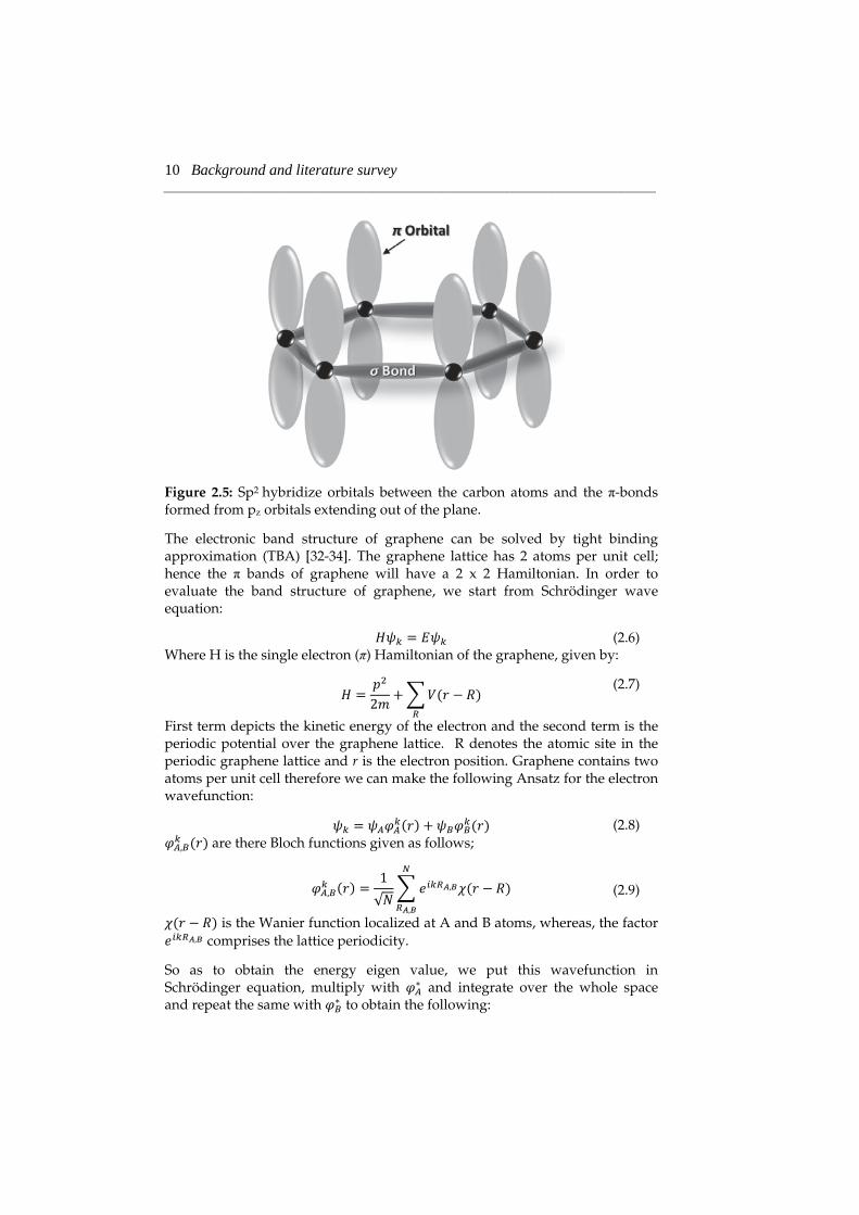
2.1.2 Electronic Structure Graphene has an amazing band structure thanks to its unique crystal structure (describe in section 2.2). Each carbon atom in graphene is tied to its three nearest neighbors via strong bonds that lie in the graphene plane with mutual angles of 120°. The forth valence electron occupies a orbital that projects above and below the molecular plane. This orbital interacts strongly with adjacent pi orbitals and allows for the delocalization of electrons between all carbon atoms within the graphene plane. This is one reason behind remarkable electrical conductivity of graphene.
10 Background and literature survey ___________________________________________________________________________________________________
Figure 2.5: Sp2 hybridize orbitals between the carbon atoms and the -bonds formed from pz orbitals extending out of the plane.
The electronic band structure of graphene can be solved by tight binding approximation (TBA) [32-34]. The graphene lattice has 2 atoms per unit cell; hence the bands of graphene will have a 2 x 2 Hamiltonian. In order to evaluate the band structure of graphene, we start from Schrödinger wave equation:
(2.6) Where H is the single electron ( ) Hamiltonian of the graphene, given by:
(2.7)
First term depicts the kinetic energy of the electron and the second term is the periodic potential over the graphene lattice. R denotes the atomic site in the periodic graphene lattice and r is the electron position. Graphene contains two atoms per unit cell therefore we can make the following Ansatz for the electron wavefunction:
(2.8) are there Bloch functions given as follows;
(2.9)
is the Wanier function localized at A and B atoms, whereas, the factor comprises the lattice periodicity.
So as to obtain the energy eigen value, we put this wavefunction in Schrödinger equation, multiply with and integrate over the whole space and repeat the same with to obtain the following:
Background and literature survey 11 ___________________________________________________________________________________________________
(2.10a)
(2.10b)
It is important to note here that do not depend on r, thus can be pulled out of these integrals. We introduce the following impression here:
(2.11a)
(2.11b)
is termed as transfer integral matrix element and describes the hopping of the electron within different carbon atoms. is termed as the overlap integral matrix element and describes the strength of the overlap of the orbitals of different atoms. We can express the equation in the matrix notation as given by:
(2.12)
For a good approximation, we only take into account the nearest neighbor interactions. Thus the off-diagonal elements need to be calculated.
(2.13)
By inserting the Bloch functions, we have
(2.14)
The term in the exponentional corresponds to the vectors l where
(l=1,2,3), since each atom has 3 nearest neighbors. Thus we can write the equation as
(2.15)
We denote the integral term as
(2.16)
Where “t” is the nearest neighbor hopping energy (hopping between different sublattices). Its value has been calculated to be around 2.8 eV [32]. The we can write
(2.17)
12 Background and literature survey ___________________________________________________________________________________________________
Where f(k) is the geometrical factor and can be calculated by simple geometry, taking into account the values for the 3 nearest neighbor vectors ( l). It is quite obvious that the other off-diagonal element can be evaluated as follows:
(2.18) We employ the same route of inserting the Bloch functions into the equation to evaluate overlap integral matrix element.
(2.19a)
(2.19b)
The Wannier functions are normalized as . Thus, we have
(2.20) For the off-diagonal term, we proceed in a similar manner.
(2.21a)
(2.21b)
(2.21c)
(2.21d)
(2.21e)
Where
(2.22)
This term describes the Wannier function overlaps of the nearest neighbors and has a value of s 0.070 [35]. As this value is very small, we can neglect the off-diagonal terms. Thus we have the following results:
, (2.23)
Background and literature survey 13 ___________________________________________________________________________________________________
Now, the eigenvalues can be extracted by solving
(2.24) which results in the following energy dispersion relation:
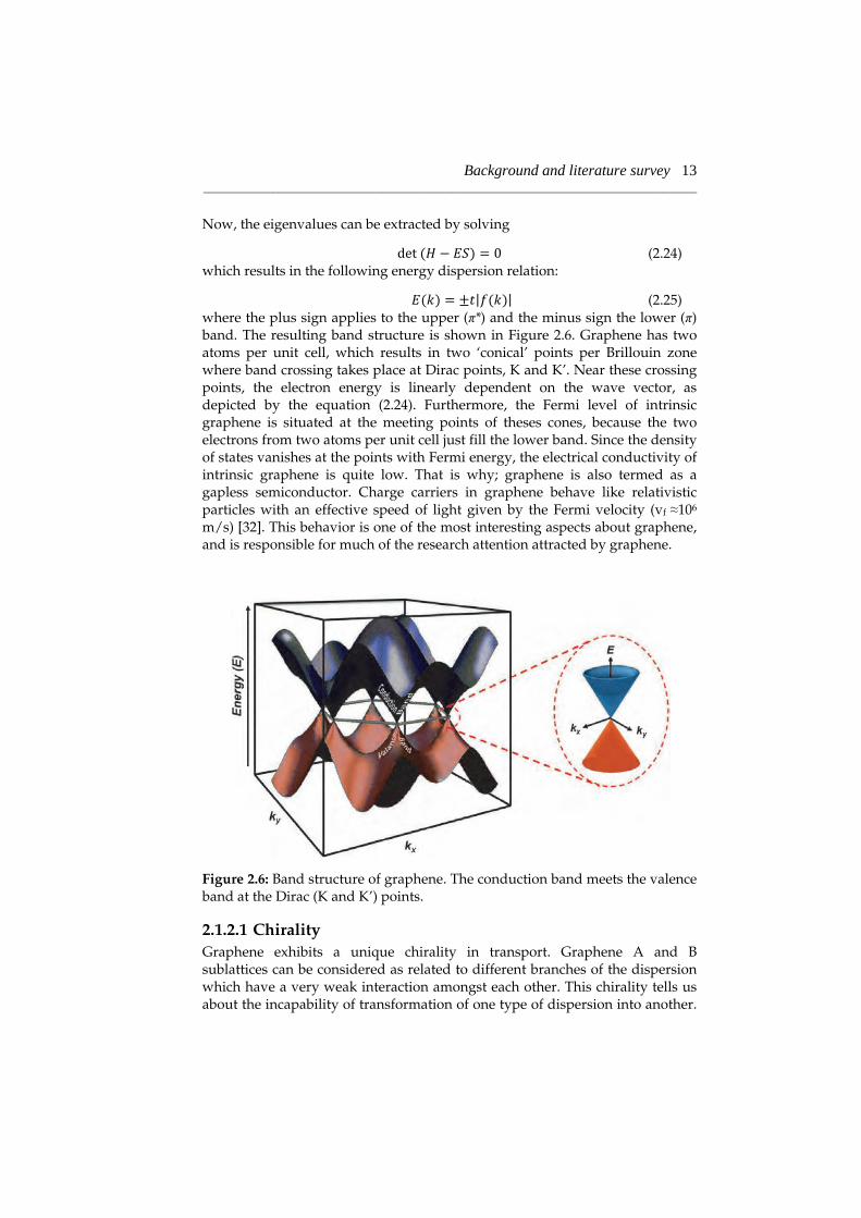
(2.25) where the plus sign applies to the upper ( *) and the minus sign the lower ( ) band. The resulting band structure is shown in Figure 2.6. Graphene has two atoms per unit cell, which results in two ‘conical’ points per Brillouin zone where band crossing takes place at Dirac points, K and K’. Near these crossing points, the electron energy is linearly dependent on the wave vector, as depicted by the equation (2.24). Furthermore, the Fermi level of intrinsic graphene is situated at the meeting points of theses cones, because the two electrons from two atoms per unit cell just fill the lower band. Since the density of states vanishes at the points with Fermi energy, the electrical conductivity of intrinsic graphene is quite low. That is why; graphene is also termed as a gapless semiconductor. Charge carriers in graphene behave like relativistic particles with an effective speed of light given by the Fermi velocity (vf 106 m/s) [32]. This behavior is one of the most interesting aspects about graphene, and is responsible for much of the research attention attracted by graphene.
Figure 2.6: Band structure of graphene. The conduction band meets the valence band at the Dirac (K and K’) points.
2.1.2.1 Chirality Graphene exhibits a unique chirality in transport. Graphene A and B sublattices can be considered as related to different branches of the dispersion which have a very weak interaction amongst each other. This chirality tells us about the incapability of transformation of one type of dispersion into another.
14 Background and literature survey ___________________________________________________________________________________________________
This chiral effect points out a pseudospin quantum number for the charge carriers. This quantum number is comparable to spin but is totally independent of the real spin. This concept of pseudospin lets us single out contributions from any of the two sublattices [36].
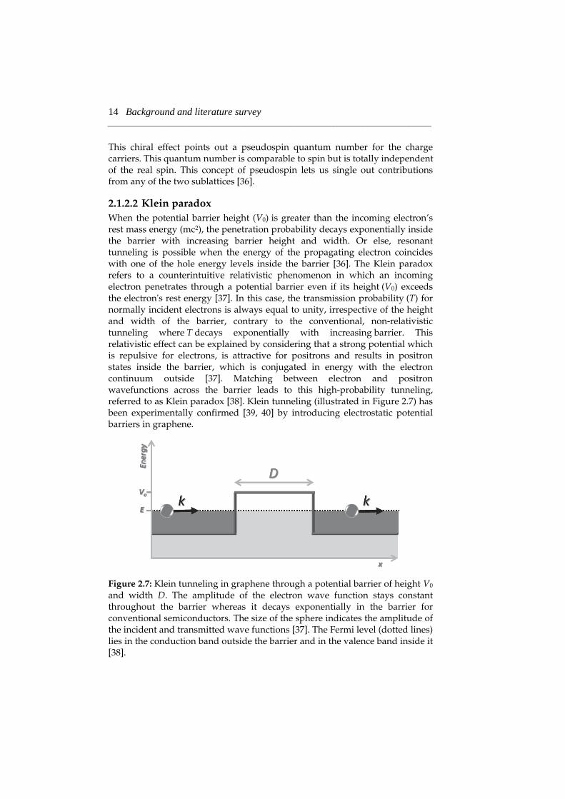
2.1.2.2 Klein paradox When the potential barrier height (V0) is greater than the incoming electron’s rest mass energy (mc2), the penetration probability decays exponentially inside the barrier with increasing barrier height and width. Or else, resonant tunneling is possible when the energy of the propagating electron coincides with one of the hole energy levels inside the barrier [36]. The Klein paradox refers to a counterintuitive relativistic phenomenon in which an incoming electron penetrates through a potential barrier even if its height (V0) exceeds the electron's rest energy [37]. In this case, the transmission probability (T) for normally incident electrons is always equal to unity, irrespective of the height and width of the barrier, contrary to the conventional, non-relativistic tunneling where T decays exponentially with increasing barrier. This relativistic effect can be explained by considering that a strong potential which is repulsive for electrons, is attractive for positrons and results in positron states inside the barrier, which is conjugated in energy with the electron continuum outside [37]. Matching between electron and positron wavefunctions across the barrier leads to this high-probability tunneling, referred to as Klein paradox [38]. Klein tunneling (illustrated in Figure 2.7) has been experimentally confirmed [39, 40] by introducing electrostatic potential barriers in graphene.
Figure 2.7: Klein tunneling in graphene through a potential barrier of height V0 and width D. The amplitude of the electron wave function stays constant throughout the barrier whereas it decays exponentially in the barrier for conventional semiconductors. The size of the sphere indicates the amplitude of the incident and transmitted wave functions [37]. The Fermi level (dotted lines) lies in the conduction band outside the barrier and in the valence band inside it [38].
Background and literature survey 15 ___________________________________________________________________________________________________
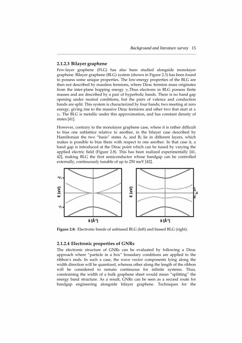
2.1.2.3 Bilayer graphene Few-layer graphene (FLG) has also been studied alongside monolayer graphene. Bilayer graphene (BLG) system (shown in Figure 2.3) has been found to possess some unique properties. The low-energy properties of the BLG are then not described by massless fermions, where Dirac fermion mass originates from the inter-plane hopping energy 1.Thus electrons in BLG possess finite masses and are described by a pair of hyperbolic bands. There is no band gap opening under neutral conditions, but the pairs of valence and conduction bands are split. This system is characterized by four bands; two meeting at zero energy, giving rise to the massive Dirac fermions and other two that start at ±
1. The BLG is metallic under this approximation, and has constant density of states [41].
However, contrary to the monolayer graphene case, where it is rather difficult to bias one sublattice relative to another, in the bilayer case described by Hamiltonian the two “basis” states A1 and B2 lie in different layers, which makes is possible to bias them with respect to one another. In that case it, a band gap is introduced at the Dirac point which can be tuned by varying the applied electric field (Figure 2.8). This has been realized experimentally [41, 42], making BLG the first semiconductor whose bandgap can be controlled externally, continuously tunable of up to 250 meV [42].
Figure 2.8: Electronic bands of unbiased BLG (left) and biased BLG (right).
2.1.2.4 Electronic properties of GNRs The electronic structure of GNRs can be evaluated by following a Dirac approach where “particle in a box” boundary conditions are applied to the ribbon’s ends. In such a case, the wave vector components lying along the width direction will be quantized, whereas other along the length of the ribbon will be considered to remain continuous for infinite systems. Thus, constraining the width of a bulk graphene sheet would mean “splitting” the energy band structure. As a result, GNRs can be seen as a second route for bandgap engineering alongside bilayer graphene. Techniques for the
16 Background and literature survey ___________________________________________________________________________________________________
production of GNRs can be put in two general categories, (i) chemical synthesis and (ii) lithographic patterning.
Chemical synthesis [9, 27] produces nanoribbons with smooth edges with widths in the sub-10 nm range. However, this method leads to a distribution of ribbon sizes and makes their positioning problematic. All this makes it unfeasible for industrial scale device fabrication.
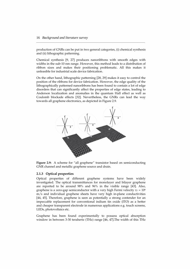
On the other hand, lithographic patterning [28, 29] makes it easy to control the position of the ribbons for device fabrication. However, the edge quality of the lithographically patterned nanoribbons has been found to contain a lot of edge disorders that can significantly affect the properties of edge states, leading to Anderson localization and anomalies in the quantum Hall effect as well as Coulomb blockade effects [32]. Nevertheless, the GNRs can lead the way towards all graphene electronics, as depicted in Figure 2.9.
Figure 2.9: A scheme for “all graphene” transistor based on semiconducting GNR channel and metallic graphene source and drain.
2.1.3 Optical properties Optical properties of different graphene systems have been widely investigated. The optical transmittances for monolayer and bilayer graphene are reported to be around 98% and 96% in the visible range [43]. Also, graphene is a zero-gap semiconductor with a very high Fermi velocity vF = 106 m/s and individual graphene sheets have very high in-plane conductivities [44, 45]. Therefore, graphene is seen as potentially a strong contender for an impeccable replacement for conventional indium tin oxide (ITO) as a better and cheaper transparent electrode in numerous applications e.g. touch screens, LEDs, photovoltaics etc.
Graphene has been found experimentally to possess optical absorption window in between 3-30 terahertz (THz) range [46, 47].The width of this THz
Background and literature survey 17 ___________________________________________________________________________________________________
window depended on the temperature and dark current densities. These findings demonstrate that graphene bilayer system can be used as novel optical and optoelectronic devices such as Terahertz phototransistors [46]. Moreover, the possibility of bandgap tuning points towards prospects of externally tuned infrared (IR) detectors.
2.1.4 Vibrational properties Phonons are the unit of vibrational energy that arises from oscillating atoms within a crystal, and their structure determines most of the electronic (also thermal and mechanical) processes in a crystal. Due to the low atomic mass of carbon and extremely strong in-plane bonding, graphene exhibits extraordinary sound velocity (~20000 km/sec) and thermal conductivity (~5000 W m-1 K-1) along the plane [48], easily outperforming CNTs in heat conduction [3]. Furthermore, vibrational properties are instrumental in understanding other graphene characteristics such as optical properties via phonon-photon scattering in Raman scattering and electronic properties through electron phonon scattering.
Vibrational properties of graphene can be well comprehended from the phonon dispersion relation [36, 49]. The two sublattices A and B are considered explicitly to solve for the eigen spectrum of the dynamical matrix, just like it was done for the electronic structure. However in this case, the atoms can vibrate in all three dimensions; hence the dynamical matrix is constructed in terms of both the sublattices as well as the 3 spatial dimensions. This leads to a dynamical 6×6 matrix, and subsequently, 6 energy eigenvalues. Two of these eigenvalues correspond to the out of plane vibrations, ZA (acoustic) and ZO (optical), and the remaining 4 correspond to the in-plane vibrations: TA (transverse acoustic), TO (transverse optical), LA (longitudinal acoustic) and LO (longitudinal optical) [36, 49, 50].
The softness of graphene is correlated with the fact that it has out of plane vibrational modes phonons that are not found in 3D solids [32]. These bending and stretching modes are the reason for the lack of long range structural order in soft membranes leading to the phenomenon of crumpling. Consequently, anharmonic coupling between bending and stretching modes results in the existence of these 2D membranes.
2.1.5 Mechanical properties The basic constitution of the graphene lattice is the C-C covalent bond which is one of the strongest bond in nature. The strength of this sp² C-C bonds gives graphene some exceptional mechanical properties, possibly better than any other material. There are several elastic parameters necessary to define the mechanical properties: e.g. the Young’s modulus (E) represents the stiffness of the material, the Poisson’s ratio ( ) gives a ratio between the transverse contraction strain to longitudinal extension and the shear modulus (G) depicts the ratio of shear stress to the shear strain.
18 Background and literature survey ___________________________________________________________________________________________________
Mechanical properties of free-standing monolayer graphene membranes have been measured experimentally by nanoindentation in an atomic force microscope. These measurements correspond to a Young’s modulus of E =1.0 ± 0.1 TPa and a third-order elastic stiffness of D = –2.0 ± 0.4 TPa, assuming an effective graphene thickness of 0.335 nm [51]. The shear modulus (G), has been reported to be 280 GPa for CVD grown graphene films [52]. Second and third-order elastic stiffness was measured to be 340 Nm–1 and 690 Nm–1, respectively. The fracture strength has been measured to be 125 GPa [53], representing the intrinsic strength of a defect free graphene sheet [51].
These exceptional values mark graphene as the strongest material ever measured, and show that graphene can be mechanically tested for deformations well beyond the linear range. These exceptional mechanical properties of graphene make it a perfect choice for application like transparent /flexible electrodes [54], reinforcement in advanced composites [53] and nanoelectromechanical systems (NEMS) [55].
Another extremely interesting phenomenon has been observed experimentally when graphene was stretched to form nanobubbles on a platinum substrate, electrons started to behave as if they were under strong magnetic fields in excess of 300 tesla, despite the fact that no magnetic field was actually applied [56]. Bandgap engineering has also been reported for strained graphene nanosheets [57].
2.2 Graphyne: A competition for graphene
Carbon have three hybridization states (sp, sp2, and sp3), allowing for numerous combinations of bonds between atoms to produce many carbon allotropes; such as naturally present graphite (sp2), diamond (sp3), and several lab synthesized allotropes such as fullerene (sp2), carbon nanotube (sp2), and graphene (sp2). With ongoing research, there are still a large number of new forms of carbon yet to be discovered. Although these carbon allotropes are extremely important, yet the study of other carbon systems was limited for most of the 20th century. In 1968, Balaban et al published an interesting article where they purposed diverse imaginative and aesthetically attractive 2- and 3D carbon allotropes [58]. Even though formation of most of these structures may be energetically impossible, some networks seemed more reasonable and thus potentially within the realm of experimental synthesis and existence.
The landmark event that energized the study of carbon allotropes was the isolation 2D monolayer graphene from 3D graphite in 2004 [2]. Apparently, it was in contradiction with the well-established theory of Landau and Peierls, which stated that 2D crystals are thermodynamically impossible to exist. This discovery paved the way for the field of 2D structures and sparked resurgence in research related to visionary carbon allotropes like graphyne and graphydine which were proposed many years back [59-61].
Background and literature survey 19 ___________________________________________________________________________________________________
Graphynes are similar to graphene, the main difference being that they have triple bonds between some of their carbon atoms [61]. Graphynes also possess Dirac cones according to rst-principles electronic structure calculations. One of these materials, “6,6,12-graphyne”, does not have hexagonal symmetry and features two self-doped nonequivalent distorted Dirac cones suggesting electronic properties as amazing as those of graphene [61].
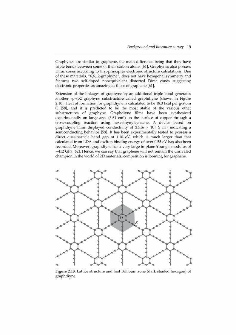
Extension of the linkages of graphyne by an additional triple bond generates another sp-sp2 graphyne substructure called graphdiyne (shown in Figure 2.10). Heat of formation for graphdiyne is calculated to be 18.3 kcal per g-atom C [58], and it is predicted to be the most stable of the various other substructures of graphyne. Graphdiyne films have been synthesized experimentally on large area (3.61 cm2) on the surface of copper through a cross-coupling reaction using hexaethynylbenzene. A device based on graphdiyne lms displayed conductivity of 2.516 × 10⁻⁴ S m-1 indicating a semiconducting behavior [59]. It has been experimentally tested to possess a direct quasiparticle band gap of 1.10 eV, which is much larger than that calculated from LDA and exciton binding energy of over 0.55 eV has also been recorded. Moreover, graphdiyne has a very large in-plane Young’s modulus of
412 GPa [62]. Hence, we can say that graphene will not remain the unrivaled champion in the world of 2D materials; competition is looming for graphene.
Figure 2.10: Lattice structure and rst Brillouin zone (dark shaded hexagon) of graphdiyne.
20 Background and literature survey ___________________________________________________________________________________________________
2.3 Properties of Zinc oxide
ZnO is an exceptional material with semiconducting and piezoelectric properties. It is seen as a vital material due to its unique properties and probably the biggest family of nanostructures. This has led to the demonstration of ZnO as an alternative material to the nitride semiconductors. The properties of ZnO will be described in this section of the chapter.
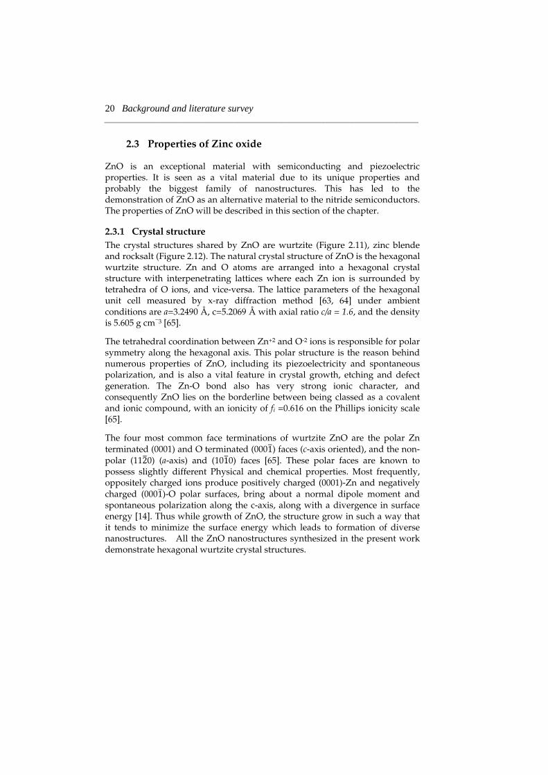
2.3.1 Crystal structure The crystal structures shared by ZnO are wurtzite (Figure 2.11), zinc blende and rocksalt (Figure 2.12). The natural crystal structure of ZnO is the hexagonal wurtzite structure. Zn and O atoms are arranged into a hexagonal crystal structure with interpenetrating lattices where each Zn ion is surrounded by tetrahedra of O ions, and vice-versa. The lattice parameters of the hexagonal unit cell measured by x-ray diffraction method [63, 64] under ambient conditions are a=3.2490 Å, c=5.2069 Å with axial ratio c/a = 1.6, and the density is 5.605 g cm 3 [65].
The tetrahedral coordination between Zn+2 and O-2 ions is responsible for polar symmetry along the hexagonal axis. This polar structure is the reason behind numerous properties of ZnO, including its piezoelectricity and spontaneous polarization, and is also a vital feature in crystal growth, etching and defect generation. The Zn-O bond also has very strong ionic character, and consequently ZnO lies on the borderline between being classed as a covalent and ionic compound, with an ionicity of fi =0.616 on the Phillips ionicity scale [65].
The four most common face terminations of wurtzite ZnO are the polar Zn terminated (0001) and O terminated (000 ) faces (c-axis oriented), and the non-polar (11 0) (a-axis) and (10 0) faces [65]. These polar faces are known to possess slightly different Physical and chemical properties. Most frequently, oppositely charged ions produce positively charged (0001)-Zn and negatively charged (000 )-O polar surfaces, bring about a normal dipole moment and spontaneous polarization along the c-axis, along with a divergence in surface energy [14]. Thus while growth of ZnO, the structure grow in such a way that it tends to minimize the surface energy which leads to formation of diverse nanostructures. All the ZnO nanostructures synthesized in the present work demonstrate hexagonal wurtzite crystal structures.
Background and literature survey 21 ___________________________________________________________________________________________________
Figure 2.11: The hexagonal wurtzite structure of ZnO. One unit cell is outlined for clarity.
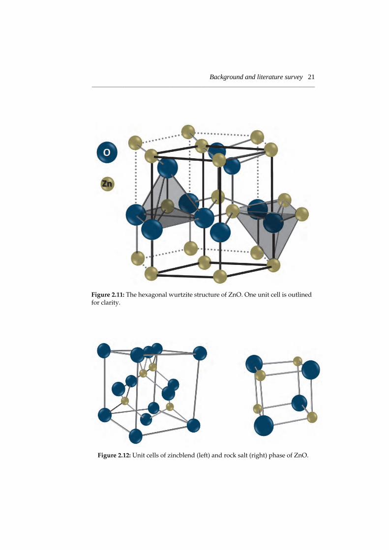
Figure 2.12: Unit cells of zincblend (left) and rock salt (right) phase of ZnO.
22 Background and literature survey ___________________________________________________________________________________________________
ZnO also exists in zincblend and rock salt phases besides the stable wurzite phase. Zincblende ZnO is stable only by growth on cubic structures e.g. by using a zinc sulphide (ZnS) buffer layer for growth of ZnO zincblend epitaxy [66]. While the rocksalt structure is a high-pressure metastable phase. Under normal conditions, wurtzite ZnO is thermodynamically stable and at pressures of about 9 GPa transforms into the cubic form. The reverse transition to wurtzite phase occurs when the pressure drops down to 2 GPa, showing large hysteresis between the direct (w rs) and reverse (rs w) phase transformations in ZnO at room temperature [67].
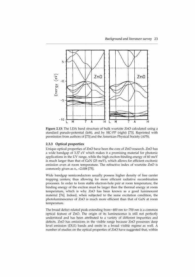
2.3.2 Electronic structure The ZnO binding in its crystal lattice involves sp3 hybridization of the electron states, resulting in four equivalent orbitals. In the resulting ZnO crystal, the bonding sp3 states create the valence band, while its antibonding states constitute the conduction band. The resulting energy gap is 3.37 eV [68, 69], which lies in the UV spectral range. Due to its wide bandgap, pure ZnO is transparent in the visible region. Moreover, a large bandgap results in higher breakdown voltages, electronic stability, lesser electronic noise and high power operation. ZnO possesses a high exciton binding energy of ~60 meV [69]. Due to the native defects such as oxygen vacancies and zinc interstitials, ZnO naturally exhibits n-type semiconductor behavior. P-type doping of ZnO is still a problem that is hindering the possibility of a ZnO p-n homojunction devices [20]
The electronic band structure of ZnO has been calculated by many groups [70-73]. The band structure has been evaluated using the local density approximation (LDA) and incorporating atomic “self-interaction-corrected-pseudo-potentials” (SIC-PP) to accurately account for the Zn 3d electrons, and is shown in Figure 2.13 [73]. Both the valence band maxima and the lowest conduction band minima occur at the point k=0 indicating direct bandgap nature of ZnO. The bottom 10 bands (occurring around 9 eV) are related to Zn 3d levels. Whereas, there are no bands in the bottom of the left panel of Figure 2.13, which is evaluated from conventional LDA method that does not account for the effect of Zn 3d levels. The next 6 bands from -5 eV to 0 eV correspond to O 2p bonding states [65, 73]. In SIC-PP incorporated LDA approximation, the bands are shifted down in energy noticeably and the band gap opening is clearly visible, as shown in right panel of the figure 2.13. The band gap calculated from this “modified LDA” method is 3.77 eV, which is in much better agreement with the experimentally evaluated value of 3.37 eV [65, 74].
Background and literature survey 23 ___________________________________________________________________________________________________
Figure 2.13: The LDA band structure of bulk wurtzite ZnO calculated using a standard pseudo-potential (left), and by SIC-PP (right) [73]. Reprinted with permission from authors of [73] and the American Physical Society (APS).
2.3.3 Optical properties Unique optical properties of ZnO have been the core of ZnO research. ZnO has a wide bandgap of 3.37 eV which makes it a promising material for photonic applications in the UV range, while the high exciton-binding energy of 60 meV is much larger than that of GaN (25 meV), which allows for efficient excitonic emission even at room temperature. The refractive index of wurtzite ZnO is commonly given as n =2.008 [75].
Wide bandgap semiconductors usually possess higher density of free carrier trapping centers; thus allowing for more efficient radiative recombination processes. In order to form stable electron-hole pair at room temperature, the binding energy of the exciton must be larger than the thermal energy at room temperature, which is why ZnO has been known as a good luminescent material [76]. Indeed, when subjected to the same excitation condition, the photoluminescence of ZnO is much more efficient than that of GaN at room temperature.
The broad defect related peak extending from 400 nm to 700 nm is a common optical feature of ZnO. The origin of its luminescence is still not perfectly understood and has been attributed to a variety of different impurities and defects. ZnO has emissions in the visible range because ZnO possesses deep level emission (DLE) bands and emits in a broad visible regime as well. A number of studies on the optical properties of ZnO have suggested that, within

24 Background and literature survey ___________________________________________________________________________________________________
the DLE, the green (~500 nm) and red (~600 nm) emissions have originated from oxygen vacancies (Vo) and zinc interstitial (Zni) [77-80]. While, some other reports attribute the green emission to both oxygen and zinc vacancies [18, 81]. The violet-blue and blue emissions were credited to zinc interstitial (Zni) and Zinc vacancies (VZn), respectively, in the DLE [18].
The yellow emission, which is mostly present in hydrothermally grown ZnO, was attributed to the presence of OH groups on the surface [77]. The formation energy and energy levels of different defects within the DLE have been experimentally studied and calculated to explain the different defect emissions (violet, blue, green, yellow, orange-red, and red) by various researchers [18, 68, 77, 80, 82, 83]. An extensive interest is being shown in investigating the defect emissions in ZnO in general and, ZnO nanostructures in particular, because of their great potential for a wide range of optical applications.
Figure 2.14: Schematic band diagram of the DLE emissions in ZnO based on the value of different impurities and the defects extracted from literature [18, 68, 77, 80, 82, 83].
2.3.4 Mechanical and piezoelectric properties The mechanical properties of a material are described by various parameters such as hardness, stiffness, and piezoelectric constants; Young’s and bulk moduli, and shear modulus. Mechanical properties of ZnO have been measured experimentally by nanoindentation in an atomic force microscope. These measurements correspond to a Young’s modulus of E = 111.2 ± 4.7 GPa and a bulk hardness of H = 5.0 ± 0.1 GPa for a plastic penetration depth of 300 nm [84]. Epitaxial Young’s modulus of E = 310±40 GPa and epitaxial hardness of 5.75±0.8 GPa has been measured for ZnO epitaxial layers grown on c-axis sapphire [85].
Background and literature survey 25 ___________________________________________________________________________________________________
Crystal orientation of ZnO has also been found as an influencing factor on the mechanical properties due to alignment of the basal planes. Bulk ZnO with a-axis orientation is significantly softer than c-axis material, having a hardness of
2 GPa at a plastic penetration depth of 50 nm [65, 85]. Basal planes lie normal to the surface in a-axis material, and are thus more vulnerable to slip-up. Results clearly indicate that epilayer ZnO is harder than its bulk counterpart, and experiences more localized contact induced deformation damage [65, 85].
Nanostructures can be taken as excellent model systems to investigate the size dependence of mechanical properties, particularly the ability to tune the dimension over continuous range to investigate mechanical properties as a function of shape and size. Mechanical properties have been found to change with size and shape. The Young’s modulus of ZnO NWs with diameters smaller than about 120 nm increases dramatically with decreasing diameters reaching upto 220 GPa (for d =20nm), and is signi cantly higher than that of the larger ones whose modulus tends to that of bulk ZnO [86].
ZnO is a well-known piezoelectric material as it demonstrates efficient charge accumulations in response to applied mechanical stress. ZnO has one of the highest piezoelectric tensor among all the tetrahedrally bonded semiconductors. This property makes it an important material for various applications requiring a large electromechanical coupling [87]. The piezoelectric tensor is comprised of three independent components in hexagonal wurtzite phase, which characterize the full piezoelectric tensor. Two of these components in wurtzite phase measure the polarization produced along the c-axis at zero electric field, under a uniform strain along the c-axis or in the basal plane [88]. The spontaneous polarization along the z-axis is given by:
(2.26)
where and are the strain along the c-axis and in the basal plane, respectively, and e33 and e31 are the piezoelectric coefficients. The third independent component of the piezoelectric tensor, e15, accounts for the polarization induced by shear strain which can be neglected for simplicity. The sign of the piezoelectric tensor is generally fixed assuming that the positive direction along c-axis goes from the cation to the anion [88]. ZnO has become a material of choice for piezoelectric harvesting devices because of the ease of growth in the nanorwire and nanobelt geometries. The effective piezoelectric coefficient d33 for the (0001) face of the nanobelts has been measured by piezoresponse force microscopy. The d33 coefficient varies from 26.7 to 14.3 pmV 1 with increasing frequency of 30 to 150 kHz. These values are noticeably larger than that for bulk ZnO effective piezoelectric coefficient value of 9.9 pm V 1 [88].
26 Background and literature survey ___________________________________________________________________________________________________
2.4 Summary
Key properties of graphene and ZnO, discussed in this chapter, have been summarized in table 2.1 and table 2.2.
Property Value Reference
Lattice parameters
a=2.4612 Å ac-c=1.14 Å (ac-c =Nearest neighbor distance)
[89]
Surface area 2630 m2 g-1 [10] Thermal conductivity 5000 W m-1 K-1 [3]
Crystal structure 2D Hexagonal [90] Carrier mobility 200 000 cm2 V-1s-1 [4]
Optical transmittance 97.7% [91] Bandgap (BLG) 0- 250 meV (Tunable) [42] Fermi velocity 106 m s-1 [44] Young’s modulus 1.0 ± 0.1 TPa [51]
Fracture strength 125 GPa [53]
Table 2.1: Key properties of graphene at the room temperature
Background and literature survey 27 ___________________________________________________________________________________________________
Table 2.2: Key properties of ZnO at the room temperature
Property Value Reference
Lattice constants
a=3.25 Å c=5.21 Å
[92]
Density 5.606 gm/cm3 [65] Melting point 1975 oC [93]
Stable crystal structure Wurtzite [90] Dielectric constant 8.66 [94] Refractive index 2.008 [75, 95] Band gap 3.37 eV, Direct [74, 90] Exciton binding energy 60 meV [96] Effective mass (Electron/Hole)
0. 24 mo / 0. 59 mo
[92]
Hole mobility 5-50 cm2/V s [97] Electron mobility 100-200 cm2/V s [97] Bulk Young’s modulus 111.2 ± 4.7 GPa [84] Bulk hardness 5.0 ± 0.1 GPa [84]
Bulk effective piezoelectric coefficient
9.9 pm V 1 [88]


Growth and processing 29 ___________________________________________________________________________________________________
C h a p t e r 3
Growth and processing
In this chapter, the details of the experimental techniques used to grow and synthesis reproducible, good quality graphene and ZnO are described. These include wet chemistry routine and sublimation on SiC by high temperature chemical vapor deposition (HTCVD) for graphene, and aqueous chemical growth (ACG), electrochemical deposition (ECD) and vapor-liquid-solid (VLS) for ZnO nanostructures. These nanostructures were incorporated in devices with patterns defined by lithography, etching (dry and wet), metallization, passivation etc.
3 3.1 Substrate preparation
Graphene nanosheets and ZnO nanostructures were casted or grown on Si, SiC, SiO2, silver, gold, and aluminum substrates. The substrates were cleaned for the purpose of eliminating unwanted dirty particles, oxide layers and chemicals on the surface of substrates to ensure good quality.
First the samples (Si and SiC) were immersed in hydrofluoric acid (HF) diluted with deionized (DI) water in a proportion of 9:1 (DI-H2O: HF) for three minutes to remove native oxide layers from the surface. Then the substrates were immersed in acetone and put under sonication for 5 minutes at 40 oC and this process was repeated with isopropanol for removing any organic stuff. Between these steps the samples were washed with DI water. After this process the samples were rinsed thoroughly in running DI water for two minutes and water break test was performed by submerging the substrate in DI water and observing the film of draining water. Finally, the samples were dried by nitrogen.
For preparing graphene oxide (GO) thin films on glass slides, the glass slide was treated for 1 h in boiling piranha solution (3:1 concentration H2SO4:H2O2) prior to the thin film deposition. After 1 h, the glass slides were removed from the cleaning solution, rinsed with DI water and dried with nitrogen and vacuum oven (100 oC).
3.2 Graphene synthesis
Graphene was first extracted by Professor Andre Geim and professor K. Novolosev by utilizing scotch tape to peel away layers of carbon from graphite, and in the end successfully attaining a single layer [2]. This method is very simple and fruitful for achieving graphene nanosheets but is impractical for scaling up to industrial level. In the present research, graphene was synthesized for device applications by two different routes; (i) wet chemistry or
30 Growth and processing ___________________________________________________________________________________________________
solution based techniques, and (ii) sublimation of Si from SiC (i.e. Si-face of SiC) in HTCVD reactor.
3.2.1 Graphene by solution based techniques Graphene nanosheets and nanoribbons were synthesized in solution phase by, (a) chemically functionalizing with compounds such as hydroxyls and cations, which stabilized the sheets in water, and (b) by non-chemical, solution-phase exfoliation of graphite in certain organic solvents. We will describe these techniques in this section of the chapter.
3.2.1.1 Polycation stabilized graphene This process is carried out in two steps; (i) chemical oxidation of hydrophobic graphite to hydrophilic graphite oxide and (ii) exfoliation into graphene oxide (GO) sheets in aqueous solution. GO sheets are graphene sheets having oxygen functional groups. These GO sheets are prevented from agglomeration by electrostatic repulsion alone [98]. The low conductive GO can be reduced to highly conducting graphene by hydrazine reduction. However, the reduction of GO in aqueous solutions soon leads to agglomeration, while a stable dispersion is key to the possibility of large scale processing. In this method we were able to stabilize functionalized graphene in aqueous solution by using a polymeric imidazolium salt [99].
Graphene oxide was prepared by the modified Hummer’s method [100, 101]. The graphite flakes were first put in H2SO4 (98%, 12 mL) and kept at 80 0C for 5 h. The resulting solution was cooled down to room temperature. Mild sonication was performed in a water bath for 2 h to further delaminate graphite into small flakes. Sonication time and power is very critical as it defines the size of the resulting graphene oxide sheets. Excessive sonication leads to extremely small flakes. Then the solution was diluted with 0.5 L de ionized (DI) water and left overnight. The solution was filtered by Nylon Millipore filters after that. The resulting powder was mixed with KMnO4 and H2SO4 and put in a cooling bath under constant stirring for 1.5 h. The solution was diluted with DI water and 20 mL H2O2 (30%) was added to it.
The supernatant was collected after 12h and dispersed in dilute HCl in order to remove the metal ion residue and then was recovered by centrifugation [100, 101]. Clean GO was again dispersed in water to make a homogeneous dispersion and was centrifuged at 8000 rpm for 40 mins in order to remove the multilayer fragments. We added a polymeric imidazolium molten salt into the aqueous dispersion of GO at a ratio of 1 mg mL-1 and vigorously shook the solution for a proper mixing. The imidazolium salt used by us was polyquaternium 16 (PQ-16) which is a copolymer with 95 % molar of imidazolium chloreide and 5 % molar of vinylimidazole. Then the solution was reduced by hydrazine monohydrate at 90oC for 1 hour to obtain a stable dispersion of graphene in aqueous solution (as illustrated in Figure 3.1).
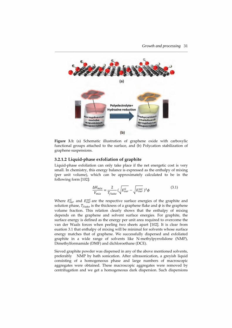
Growth and processing 31 ___________________________________________________________________________________________________
Figure 3.1: (a) Schematic illustration of graphene oxide with carboxylic functional groups attached to the surface, and (b) Polycation stabilization of graphene suspensions.
3.2.1.2 Liquid-phase exfoliation of graphite Liquid-phase exfoliation can only take place if the net energetic cost is very small. In chemistry, this energy balance is expressed as the enthalpy of mixing (per unit volume), which can be approximately calculated to be in the following form [102]:
(3.1)
Where and are the respective surface energies of the graphite and solution phase, is the thickness of a graphene flake and is the graphene volume fraction. This relation clearly shows that the enthalpy of mixing depends on the graphene and solvent surface energies. For graphite, the surface energy is defined as the energy per unit area required to overcome the van der Waals forces when peeling two sheets apart [102]. It is clear from euation 3.1 that enthalpy of mixing will be minimal for solvents whose surface energy matches that of graphene. We successfully dispersed and exfoliated graphite in a wide range of solvents like N-methylpyrrolidone (NMP), Dimethylformamide (DMF) and dichloroethane (DCE).
Sieved graphite powder was dispersed in any of the above mentioned solvents, preferably NMP by bath sonication. After ultrasonication, a greyish liquid consisting of a homogeneous phase and large numbers of macroscopic aggregates were obtained. These macroscopic aggregates were removed by centrifugation and we get a homogeneous dark dispersion. Such dispersions
32 Growth and processing ___________________________________________________________________________________________________
were prepared by varying different parameters like graphite concentrations, sonication time and centrifugation speeds. Especially, Sonication time and power is very critical as it defines the size of the resulting graphene flakes. Flakes with sizes up to 10 m were obtained by applying sonication for short time (25 mins) but concentration is very low in this case (0.01 mg mL-1) [102]. We also tested that by applying mild sonication for very long times (up to 180 h) in NMP, we can get the graphene concentration up to 1mg mL-1 [103, 104]. These graphene dispersions were found to be stable against considerable sedimentation and aggregation for several weeks. These high concentration dispersions can be used for depositing graphene thin films with good electrical, optical and mechanical properties
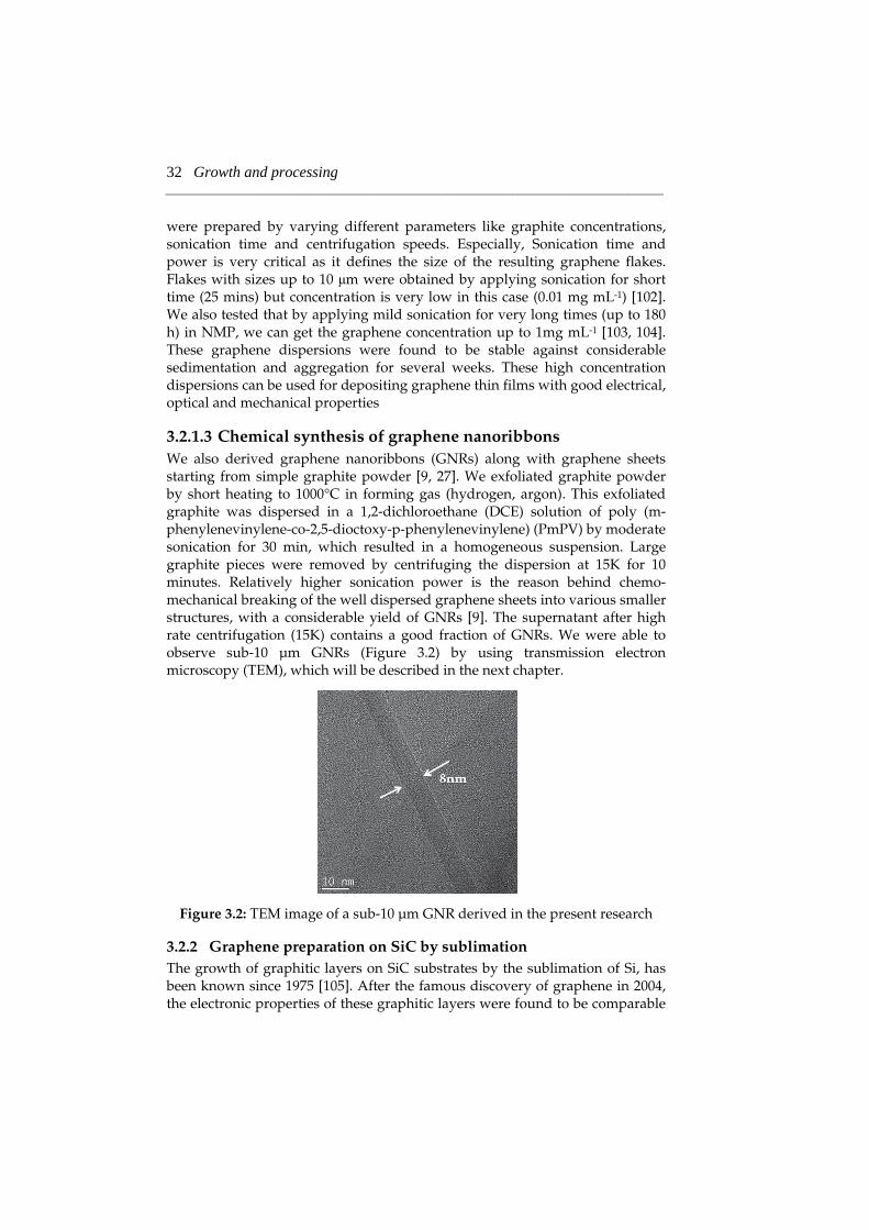
3.2.1.3 Chemical synthesis of graphene nanoribbons We also derived graphene nanoribbons (GNRs) along with graphene sheets starting from simple graphite powder [9, 27]. We exfoliated graphite powder by short heating to 1000°C in forming gas (hydrogen, argon). This exfoliated graphite was dispersed in a 1,2-dichloroethane (DCE) solution of poly (m-phenylenevinylene-co-2,5-dioctoxy-p-phenylenevinylene) (PmPV) by moderate sonication for 30 min, which resulted in a homogeneous suspension. Large graphite pieces were removed by centrifuging the dispersion at 15K for 10 minutes. Relatively higher sonication power is the reason behind chemo-mechanical breaking of the well dispersed graphene sheets into various smaller structures, with a considerable yield of GNRs [9]. The supernatant after high rate centrifugation (15K) contains a good fraction of GNRs. We were able to observe sub-10 μm GNRs (Figure 3.2) by using transmission electron microscopy (TEM), which will be described in the next chapter.
Figure 3.2: TEM image of a sub-10 μm GNR derived in the present research
3.2.2 Graphene preparation on SiC by sublimation The growth of graphitic layers on SiC substrates by the sublimation of Si, has been known since 1975 [105]. After the famous discovery of graphene in 2004, the electronic properties of these graphitic layers were found to be comparable
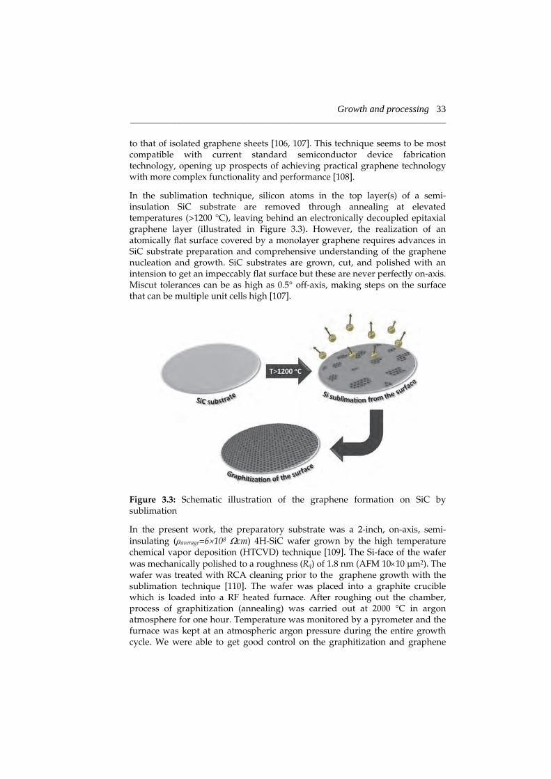
Growth and processing 33 ___________________________________________________________________________________________________
to that of isolated graphene sheets [106, 107]. This technique seems to be most compatible with current standard semiconductor device fabrication technology, opening up prospects of achieving practical graphene technology with more complex functionality and performance [108].
In the sublimation technique, silicon atoms in the top layer(s) of a semi-insulation SiC substrate are removed through annealing at elevated temperatures (>1200 °C), leaving behind an electronically decoupled epitaxial graphene layer (illustrated in Figure 3.3). However, the realization of an atomically at surface covered by a monolayer graphene requires advances in SiC substrate preparation and comprehensive understanding of the graphene nucleation and growth. SiC substrates are grown, cut, and polished with an intension to get an impeccably flat surface but these are never perfectly on-axis. Miscut tolerances can be as high as 0.5° off-axis, making steps on the surface that can be multiple unit cells high [107].
Figure 3.3: Schematic illustration of the graphene formation on SiC by sublimation
In the present work, the preparatory substrate was a 2-inch, on-axis, semi-insulating ( average=6 108 cm) 4H-SiC wafer grown by the high temperature chemical vapor deposition (HTCVD) technique [109]. The Si-face of the wafer was mechanically polished to a roughness (Rq) of 1.8 nm (AFM 10 10 μm2). The wafer was treated with RCA cleaning prior to the graphene growth with the sublimation technique [110]. The wafer was placed into a graphite crucible which is loaded into a RF heated furnace. After roughing out the chamber, process of graphitization (annealing) was carried out at 2000 °C in argon atmosphere for one hour. Temperature was monitored by a pyrometer and the furnace was kept at an atmospheric argon pressure during the entire growth cycle. We were able to get good control on the graphitization and graphene
34 Growth and processing ___________________________________________________________________________________________________
monolayer was found with good coverage on the surface. The details about the quality of as derived graphene will be discussed in the coming chapter.
3.3 Growth of ZnO nanostructures
ZnO has possibly the richest family of nanostructures among all materials, both in structures and properties [14]. A variety of ZnO nanostructures, such as nanowires, nanotubes, nanofibers, nanospheres and nano-tetrapods, nano-cabbage, nanocombs, nanowalls and nanoprisms have been successfully grown by different methods including VLS technique, thermal evaporation, low temperature aqueous chemical growth (ACG), electrodeposition, etc [68, 111-114]. ZnO nanostructures in this work were mainly synthesized by ACG and VLS methods.
3.3.1 Aqueous chemical growth (ACG) There have been many reports on the synthesis of ZnO structures by solution based methods. Zinc nitrate, zinc acetate and zinc chloride have been used as zinc sources, while HMT (hexamethyletetramine), CTAB (cetyltrimethylammonium), PPA (poly acrylic acid), SDS (sodium dodecyl sulfate), ethanol and PVP (polyvinylpyrrolidone) have all been used as chemical additives, surfactants and modifiers to alter the morphology of the ZnO nanostructures [115].
The growth of ZnO nanorods (NRs) or nanowires (NWs) from aqueous solution involves controlled heterogenous nucleation and homogeneous nucleation on the substrate. In this chemical solution, the HMT decomposes to formaldehyde and ammonia, which act as a pH buffer to regulate the pH value of the solution and also supplies additional OH- ions [116, 117]. Through the whole experiment, the pH value is retained neutral in general cases. The main chemical process can be described as
(3.2)
(3.3)
(3.4)
(3.5)
Additional OH- ions are attained by the chemical reaction of HMT with water:
(3.6)
(3.7)
HMT also contributes dominantly in defining the shape and morphology of the nanostructures [118]. HMT is a long chain polymer and a nonpolar chelating
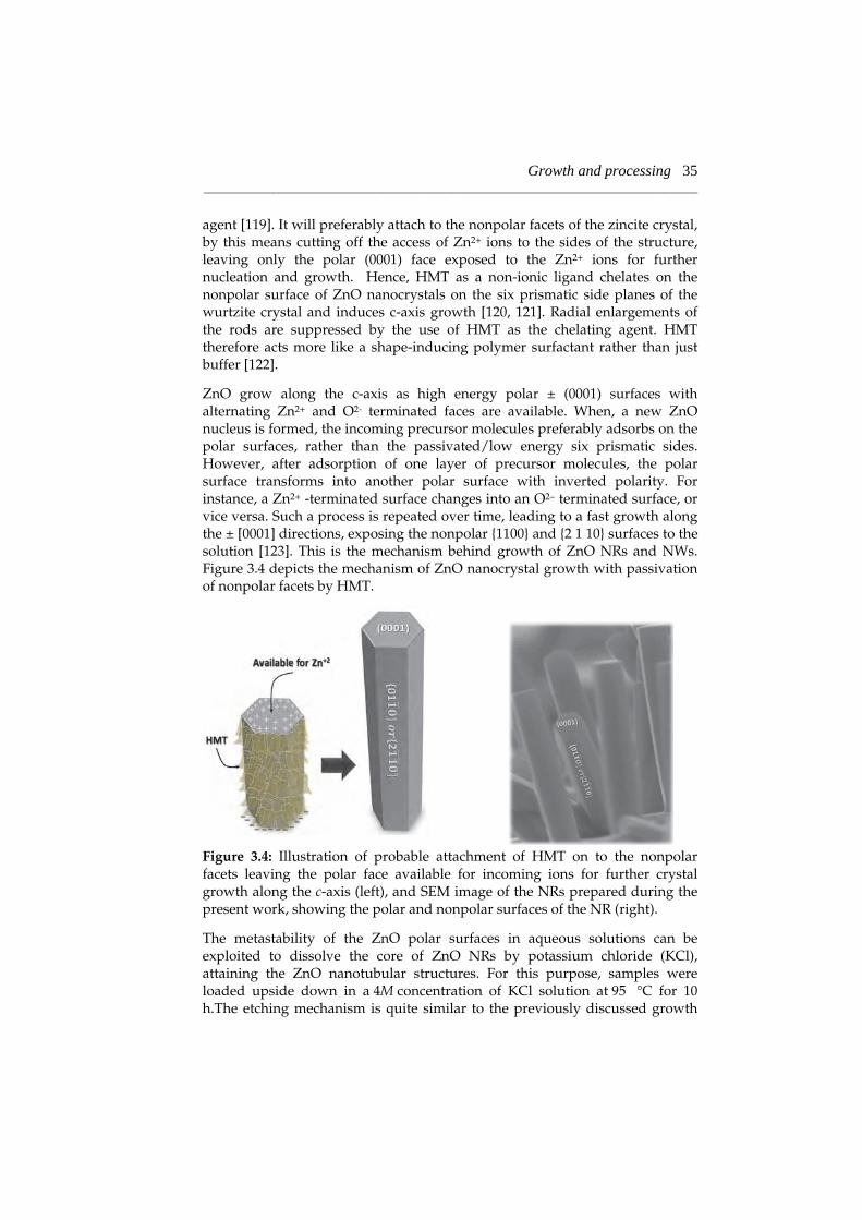
Growth and processing 35 ___________________________________________________________________________________________________
agent [119]. It will preferably attach to the nonpolar facets of the zincite crystal, by this means cutting off the access of Zn2+ ions to the sides of the structure, leaving only the polar (0001) face exposed to the Zn2+ ions for further nucleation and growth. Hence, HMT as a non-ionic ligand chelates on the nonpolar surface of ZnO nanocrystals on the six prismatic side planes of the wurtzite crystal and induces c-axis growth [120, 121]. Radial enlargements of the rods are suppressed by the use of HMT as the chelating agent. HMT therefore acts more like a shape-inducing polymer surfactant rather than just buffer [122].
ZnO grow along the c-axis as high energy polar ± (0001) surfaces with alternating Zn2+ and O2- terminated faces are available. When, a new ZnO nucleus is formed, the incoming precursor molecules preferably adsorbs on the polar surfaces, rather than the passivated/low energy six prismatic sides. However, after adsorption of one layer of precursor molecules, the polar surface transforms into another polar surface with inverted polarity. For instance, a Zn2+ -terminated surface changes into an O2– terminated surface, or vice versa. Such a process is repeated over time, leading to a fast growth along the ± [0001] directions, exposing the nonpolar {1100} and {2 1 10} surfaces to the solution [123]. This is the mechanism behind growth of ZnO NRs and NWs. Figure 3.4 depicts the mechanism of ZnO nanocrystal growth with passivation of nonpolar facets by HMT.
Figure 3.4: Illustration of probable attachment of HMT on to the nonpolar facets leaving the polar face available for incoming ions for further crystal growth along the c-axis (left), and SEM image of the NRs prepared during the present work, showing the polar and nonpolar surfaces of the NR (right).
The metastability of the ZnO polar surfaces in aqueous solutions can be exploited to dissolve the core of ZnO NRs by potassium chloride (KCl), attaining the ZnO nanotubular structures. For this purpose, samples were loaded upside down in a 4M concentration of KCl solution at 95�°C for 10 h.The etching mechanism is quite similar to the previously discussed growth
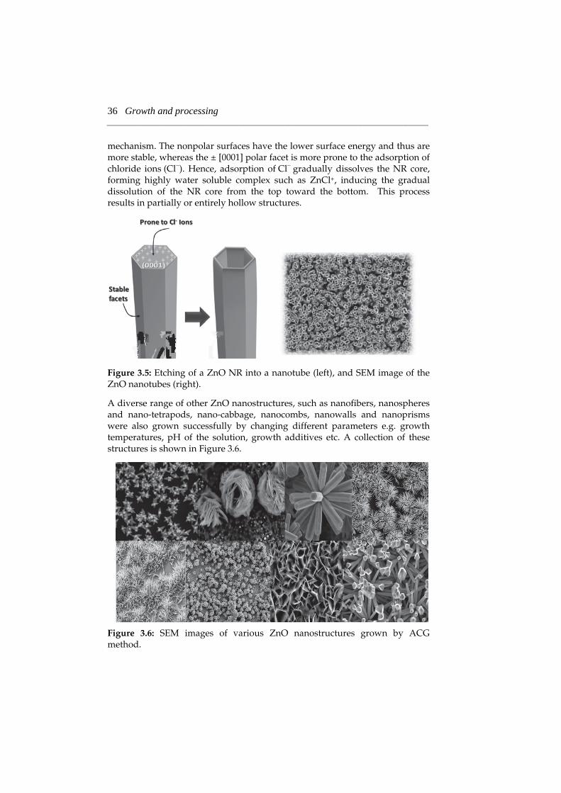
36 Growth and processing ___________________________________________________________________________________________________
mechanism. The nonpolar surfaces have the lower surface energy and thus are more stable, whereas the ± [0001] polar facet is more prone to the adsorption of chloride ions (Cl ). Hence, adsorption of Cl gradually dissolves the NR core, forming highly water soluble complex such as ZnCl+, inducing the gradual dissolution of the NR core from the top toward the bottom. This process results in partially or entirely hollow structures.
Figure 3.5: Etching of a ZnO NR into a nanotube (left), and SEM image of the ZnO nanotubes (right).
A diverse range of other ZnO nanostructures, such as nanofibers, nanospheres and nano-tetrapods, nano-cabbage, nanocombs, nanowalls and nanoprisms were also grown successfully by changing different parameters e.g. growth temperatures, pH of the solution, growth additives etc. A collection of these structures is shown in Figure 3.6.
Figure 3.6: SEM images of various ZnO nanostructures grown by ACG method.
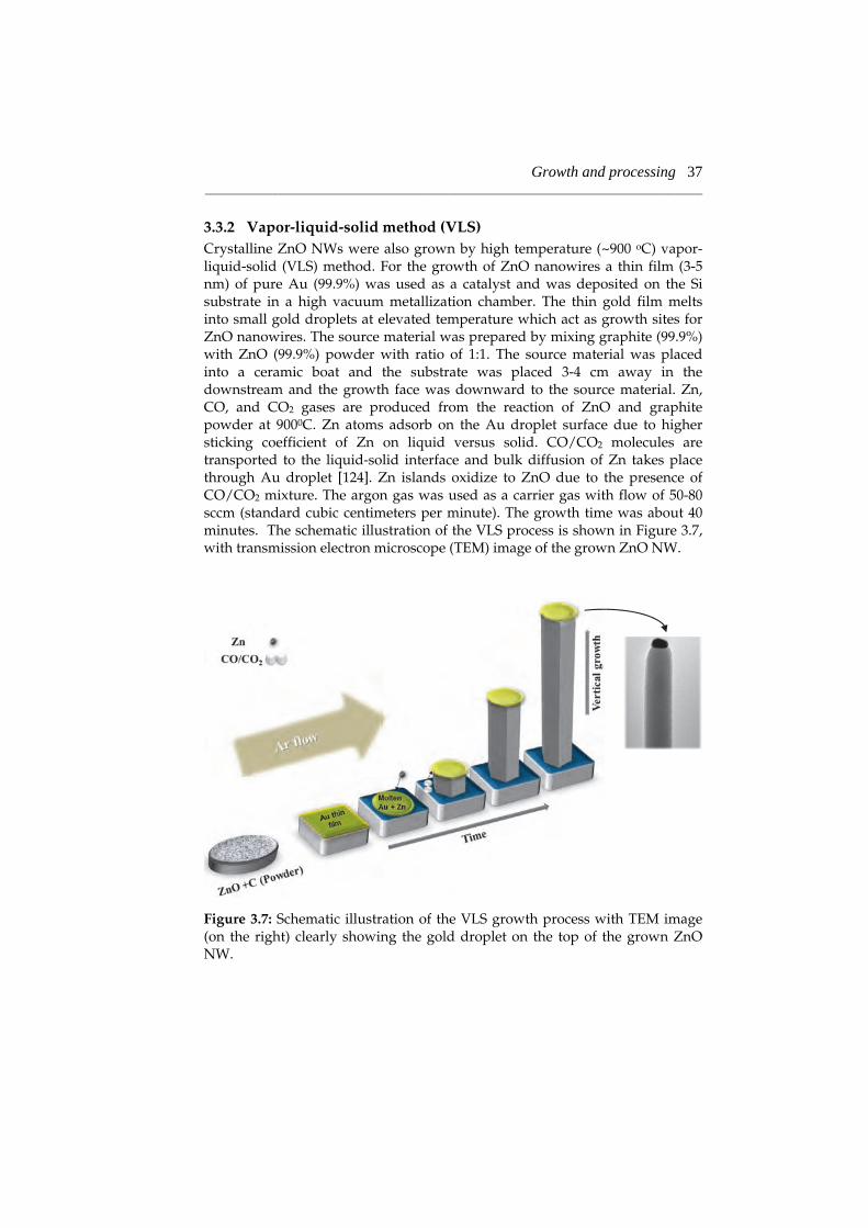
Growth and processing 37 ___________________________________________________________________________________________________
3.3.2 Vapor-liquid-solid method (VLS) Crystalline ZnO NWs were also grown by high temperature (~900 oC) vapor-liquid-solid (VLS) method. For the growth of ZnO nanowires a thin film (3-5 nm) of pure Au (99.9%) was used as a catalyst and was deposited on the Si substrate in a high vacuum metallization chamber. The thin gold film melts into small gold droplets at elevated temperature which act as growth sites for ZnO nanowires. The source material was prepared by mixing graphite (99.9%) with ZnO (99.9%) powder with ratio of 1:1. The source material was placed into a ceramic boat and the substrate was placed 3-4 cm away in the downstream and the growth face was downward to the source material. Zn, CO, and CO2 gases are produced from the reaction of ZnO and graphite powder at 9000C. Zn atoms adsorb on the Au droplet surface due to higher sticking coefficient of Zn on liquid versus solid. CO/CO2 molecules are transported to the liquid-solid interface and bulk diffusion of Zn takes place through Au droplet [124]. Zn islands oxidize to ZnO due to the presence of CO/CO2 mixture. The argon gas was used as a carrier gas with flow of 50-80 sccm (standard cubic centimeters per minute). The growth time was about 40 minutes. The schematic illustration of the VLS process is shown in Figure 3.7, with transmission electron microscope (TEM) image of the grown ZnO NW.
Figure 3.7: Schematic illustration of the VLS growth process with TEM image (on the right) clearly showing the gold droplet on the top of the grown ZnO NW.
38 Growth and processing ___________________________________________________________________________________________________
3.4 Device processing
The fabrication of devices involves several different patterns, deposited in very controlled amounts over small regions with full precision. The various patterns used in device patterning, metallization and etching are defined by a process called lithography.
The lithography process employed during the present research generally consisted of the several steps. A photoresist (PR) is first spin-coated on the surface of the substrate. The resist layer is then selectively exposed to ultraviolet (UV) radiation through a photomask. After exposure, the PR is developed which removes the unwanted areas of the PR layer, revealing the corresponding areas of the underlying layer. The development step may remove either the exposed or unexposed areas depending on the resist type (positive or negative). Within the developed pattern, the areas with no resist material left on top of them were then subjected to subtractive (etching) or additive (metallization, passivation etc.) processes, permitting the selective removal or deposition of material on the substrate.
Etching is the process of removing regions of the underlying material that are no longer protected by photoresist after development. Etching processes can be isotropic or anisotropic, depending on the type. Wet etching is generally isotropic, whereas, dry etching processes that employ reactive plasmas are generally anisotropic. Reactive plasma or reactive ion etching (RIE) involves the removal of surface material not protected by lithographic masks by impinging chemically reactive species. These species are generally oxidizing and reducing agents produced from process gases that have been ionized by a glow discharge. The ion plasma reacts with the exposed surface material, removing them from the substrate while forming volatile byproducts in the process. In some cases, hard metal (Ni, Al) masks were also used while performing high power RIE process, in order to avoid the PR burning effect.
Metallization was performed inside a high vacuum (P <10-6 Torr) metallization chamber, mainly by resistive heating. In some cases, simple shadow masks were also used but generally PR patterned masks were used followed by the lift-off process. Passivation layers of silicon dioxide (SiO2) and silicon nitride (Si3N4) were deposited by plasma enhanced chemical vapor deposition (PECVD) process.
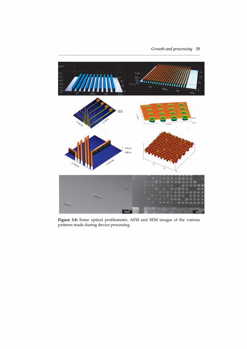
Growth and processing 39 ___________________________________________________________________________________________________
Figure 3.8: Some optical profilometer, AFM and SEM images of the various patterns made during device processing

40 Growth and processing ___________________________________________________________________________________________________
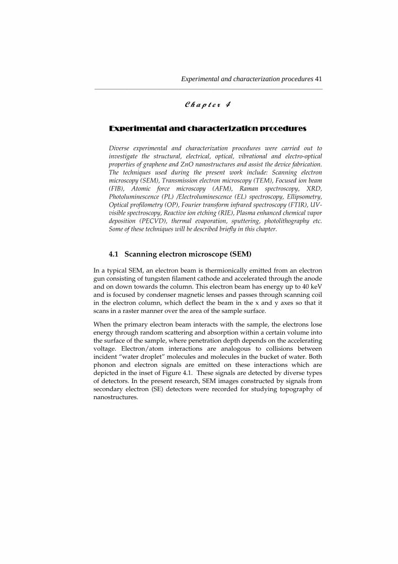
Experimental and characterization procedures 41 ___________________________________________________________________________________________________
C h a p t e r 4
Experimental and characterization procedures
Diverse experimental and characterization procedures were carried out to investigate the structural, electrical, optical, vibrational and electro-optical properties of graphene and ZnO nanostructures and assist the device fabrication. The techniques used during the present work include: Scanning electron microscopy (SEM), Transmission electron microscopy (TEM), Focused ion beam (FIB), Atomic force microscopy (AFM), Raman spectroscopy, XRD, Photoluminescence (PL) /Electroluminescence (EL) spectroscopy, Ellipsometry, Optical profilometry (OP), Fourier transform infrared spectroscopy (FTIR), UV-visible spectroscopy, Reactive ion etching (RIE), Plasma enhanced chemical vapor deposition (PECVD), thermal evaporation, sputtering, photolithography etc. Some of these techniques will be described briefly in this chapter.
4
4.1 Scanning electron microscope (SEM)
In a typical SEM, an electron beam is thermionically emitted from an electron gun consisting of tungsten filament cathode and accelerated through the anode and on down towards the column. This electron beam has energy up to 40 keV and is focused by condenser magnetic lenses and passes through scanning coil in the electron column, which deflect the beam in the x and y axes so that it scans in a raster manner over the area of the sample surface.
When the primary electron beam interacts with the sample, the electrons lose energy through random scattering and absorption within a certain volume into the surface of the sample, where penetration depth depends on the accelerating voltage. Electron/atom interactions are analogous to collisions between incident “water droplet” molecules and molecules in the bucket of water. Both phonon and electron signals are emitted on these interactions which are depicted in the inset of Figure 4.1. These signals are detected by diverse types of detectors. In the present research, SEM images constructed by signals from secondary electron (SE) detectors were recorded for studying topography of nanostructures.
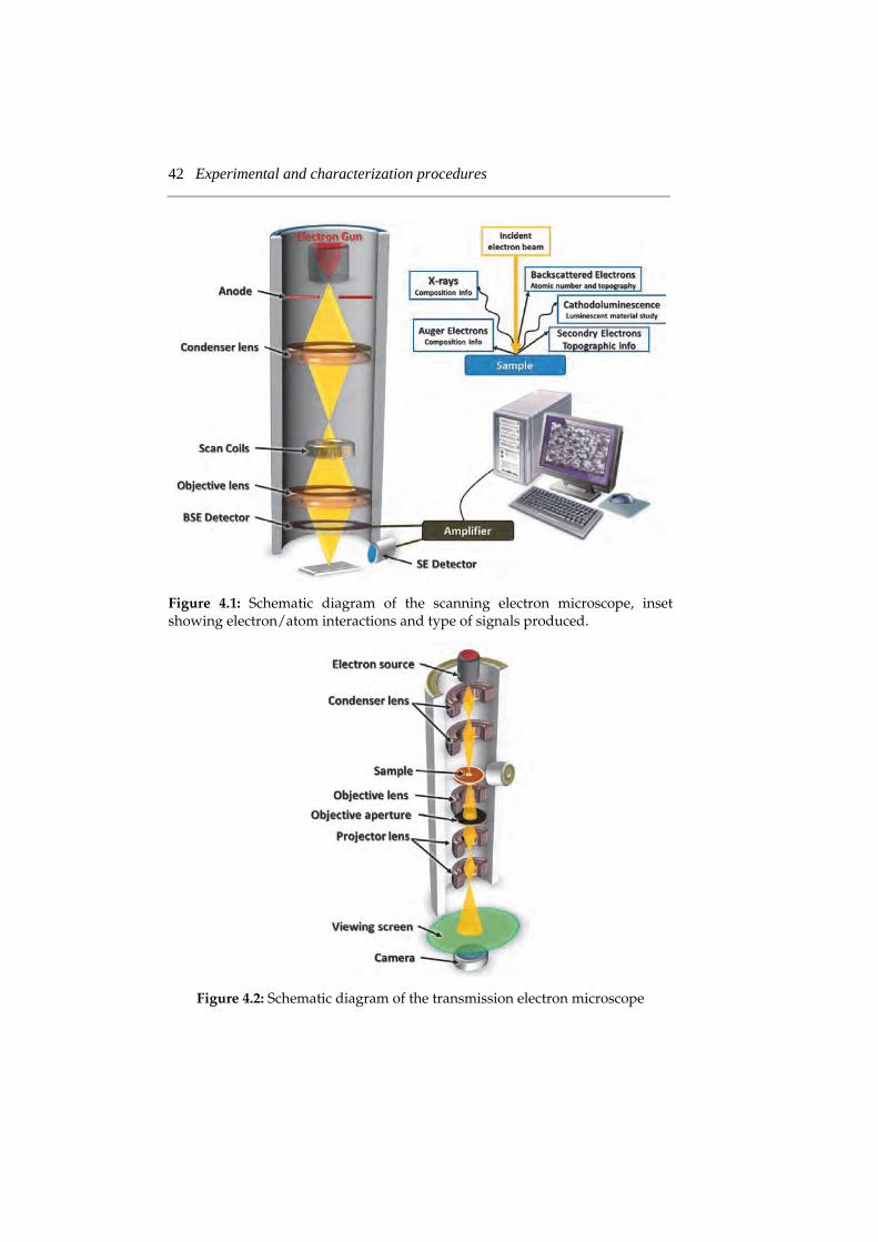
42 Experimental and characterization procedures ___________________________________________________________________________________________________
Figure 4.1: Schematic diagram of the scanning electron microscope, inset showing electron/atom interactions and type of signals produced.
Figure 4.2: Schematic diagram of the transmission electron microscope
Experimental and characterization procedures 43 ___________________________________________________________________________________________________
4.2 Transmission electron microscope (TEM)
Transmission electron microscopy (TEM) is a microscopy technique in which a beam of electrons is focused on the sample in somewhat similar manner like SEM but in this case beam is transmitted through the ultra-thin sample, interacting with the atoms of the sample as it passes through. An image is formed from the interaction of the electrons transmitted through the specimen; the image is magnified and focused onto an imaging device, such as a fluorescent screen or CCD camera. Working principle of TEM is quite similar to an ordinary light projector. TEM has many advantages over SEM e.g. superior spatial resolution, large range of operation, simultaneous reciprocal and real space information etc. While the disadvantages include destructive and extensive sample preparation process (most of the time), extremely local information and relatively difficult operation and interpretation procedures. The obtained information from TEM is related to the bulk, thus it is in general not a surface sensitive technique. The schematic illustration of the TEM setup is shown in Figure 4.2.
4.3 Focused ion beam (FIB)
The Focused Ion Beam (FIB) system resembles to a scanning electron microscope (SEM) in operation, but instead of a beam of electrons, it uses a focused beam of gallium ions (Ga+) that can be used for imaging at low beam currents or for precisely controlled sputtering or milling at high beam currents.
Gallium (Ga+) primary ion beam hits the sample surface and sputters some material, which leaves the surface as secondary ions (i+ or i-) or neutral atoms (n0). The beam impact also produces secondary electrons (e-). The signal from the sputtered ions or secondary electrons can be collected to form images. By introducing minute amounts of gas near to the sample surface at the same time as the beam is scanning, the FIB can accurately deposit or etch material. These gases are introduced close to the sample surface via a high precision gas injection system (GIS). Carbon (C), platinum (Pt), tungsten (W), palladium (Pd) and silicon dioxide (SiO2) are examples of the species that can be deposited. FIB is also integrated in a system with both electron and ion beam columns, where electron beam is used for imaging and ion beam for selected milling or deposition. FIB working principle and SEM images of the selective milling and metal deposition are shown in Figure 4.3.
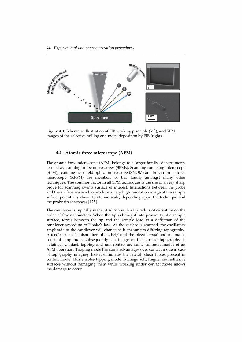
44 Experimental and characterization procedures ___________________________________________________________________________________________________
Figure 4.3: Schematic illustration of FIB working principle (left), and SEM images of the selective milling and metal deposition by FIB (right).
4.4 Atomic force microscope (AFM)
The atomic force microscope (AFM) belongs to a larger family of instruments termed as scanning probe microscopes (SPMs). Scanning tunneling microscope (STM), scanning near field optical microscope (SNOM) and kelvin probe force microscopy (KPFM) are members of this family amongst many other techniques. The common factor in all SPM techniques is the use of a very sharp probe for scanning over a surface of interest. Interactions between the probe and the surface are used to produce a very high resolution image of the sample suface, potentially down to atomic scale, depending upon the technique and the probe tip sharpness [125].
The cantilever is typically made of silicon with a tip radius of curvature on the order of few nanometers. When the tip is brought into proximity of a sample surface, forces between the tip and the sample lead to a deflection of the cantilever according to Hooke's law. As the surface is scanned, the oscillatory amplitude of the cantilever will change as it encounters differing topography. A feedback mechanism alters the z-height of the piezo crystal and maintains constant amplitude, subsequently; an image of the surface topography is obtained. Contact, tapping and non-contact are some common modes of an AFM operation. Tapping mode has some advantages over contact mode in case of topography imaging, like it eliminates the lateral, shear forces present in contact mode. This enables tapping mode to image soft, fragile, and adhesive surfaces without damaging them while working under contact mode allows the damage to occur.
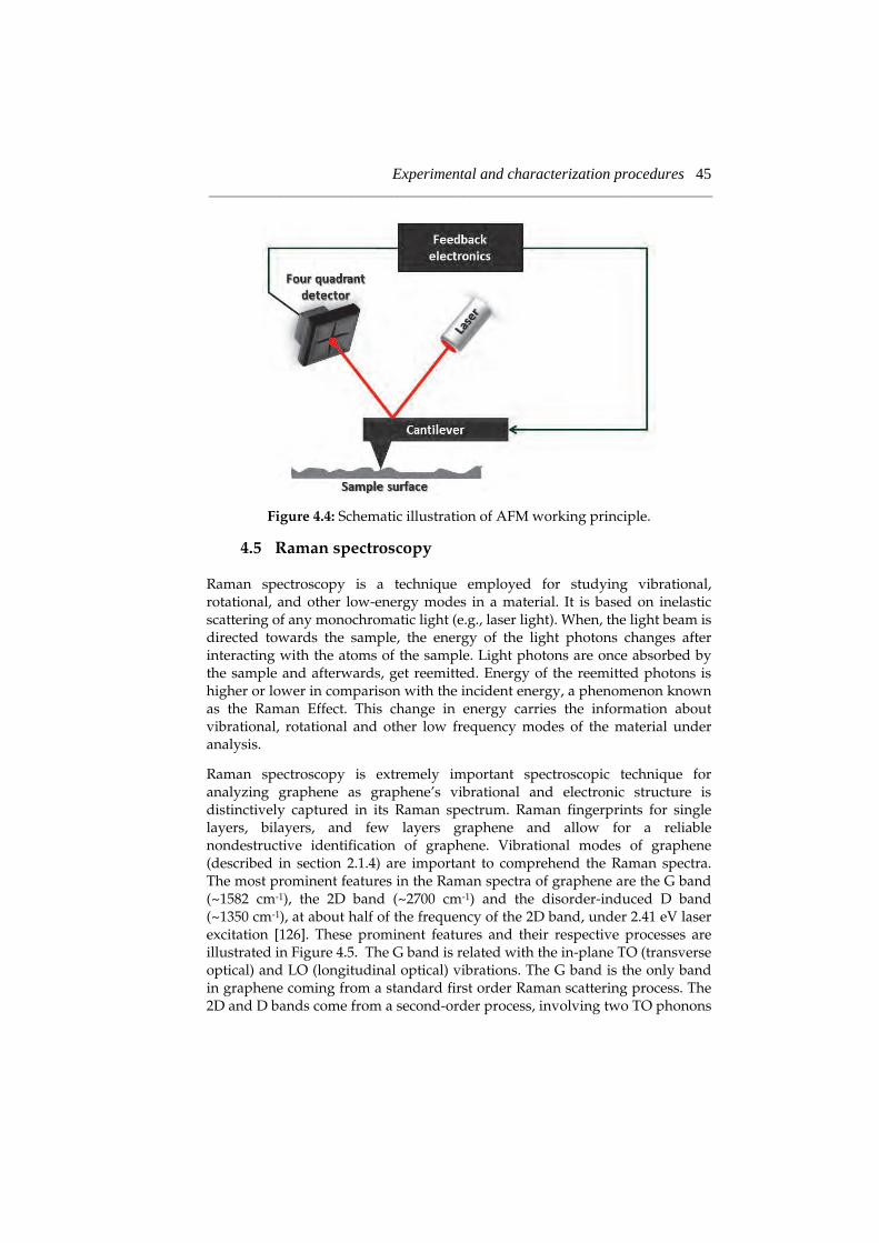
Experimental and characterization procedures 45 ___________________________________________________________________________________________________
Figure 4.4: Schematic illustration of AFM working principle.
4.5 Raman spectroscopy
Raman spectroscopy is a technique employed for studying vibrational, rotational, and other low-energy modes in a material. It is based on inelastic scattering of any monochromatic light (e.g., laser light). When, the light beam is directed towards the sample, the energy of the light photons changes after interacting with the atoms of the sample. Light photons are once absorbed by the sample and afterwards, get reemitted. Energy of the reemitted photons is higher or lower in comparison with the incident energy, a phenomenon known as the Raman Effect. This change in energy carries the information about vibrational, rotational and other low frequency modes of the material under analysis.
Raman spectroscopy is extremely important spectroscopic technique for analyzing graphene as graphene’s vibrational and electronic structure is distinctively captured in its Raman spectrum. Raman fingerprints for single layers, bilayers, and few layers graphene and allow for a reliable nondestructive identification of graphene. Vibrational modes of graphene (described in section 2.1.4) are important to comprehend the Raman spectra. The most prominent features in the Raman spectra of graphene are the G band (~1582 cm-1), the 2D band (~2700 cm-1) and the disorder-induced D band (~1350 cm-1), at about half of the frequency of the 2D band, under 2.41 eV laser excitation [126]. These prominent features and their respective processes are illustrated in Figure 4.5. The G band is related with the in-plane TO (transverse optical) and LO (longitudinal optical) vibrations. The G band is the only band in graphene coming from a standard first order Raman scattering process. The 2D and D bands come from a second-order process, involving two TO phonons
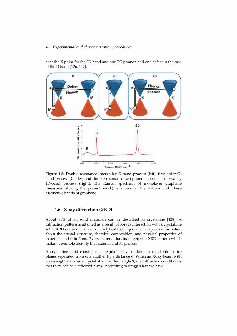
46 Experimental and characterization procedures ___________________________________________________________________________________________________
near the K point for the 2D band and one TO phonon and one defect in the case of the D band [126, 127].
Figure 4.5: Double resonance intervalley D-band process (left), first order G-band process (Center) and double resonance two phonons assisted intervalley 2D-band process (right). The Raman spectrum of monolayer graphene (measured during the present work) is shown at the bottom with these distinctive bands of graphene.
4.6 X-ray diffraction (XRD)
About 95% of all solid materials can be described as crystalline [128]. A diffraction pattern is attained as a result of X-rays interaction with a crystalline solid. XRD is a non-destructive analytical technique which exposes information about the crystal structure, chemical composition, and physical properties of materials and thin films. Every material has its fingerprint XRD pattern which makes it possible identify the material and its phases.
A crystalline solid consists of a regular array of atoms, stacked into lattice planes separated from one another by a distance d. When an X-ray beam with wavelength strikes a crystal at an incident angle , if a diffraction condition is met there can be a reflected X-ray. According to Bragg’s law we have:
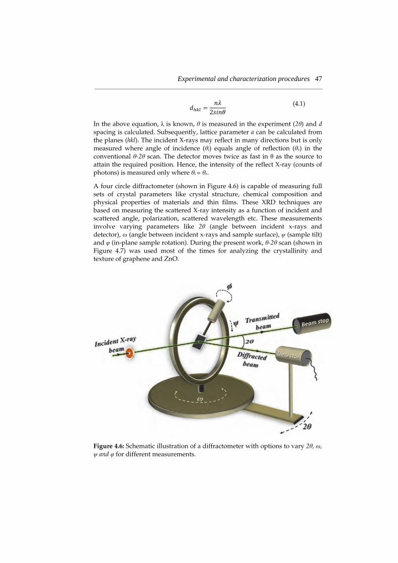
Experimental and characterization procedures 47 ___________________________________________________________________________________________________
(4.1)
In the above equation, is known, is measured in the experiment (2 ) and d spacing is calculated. Subsequently, lattice parameter a can be calculated from the planes (hkl). The incident X-rays may reflect in many directions but is only measured where angle of incidence ( i) equals angle of reflection ( r) in the conventional -2 scan. The detector moves twice as fast in as the source to attain the required position. Hence, the intensity of the reflect X-ray (counts of photons) is measured only where i = r.
A four circle diffractometer (shown in Figure 4.6) is capable of measuring full sets of crystal parameters like crystal structure, chemical composition and physical properties of materials and thin films. These XRD techniques are based on measuring the scattered X-ray intensity as a function of incident and scattered angle, polarization, scattered wavelength etc. These measurements involve varying parameters like 2 (angle between incident x-rays and detector), (angle between incident x-rays and sample surface), (sample tilt) and (in-plane sample rotation). During the present work, -2 scan (shown in Figure 4.7) was used most of the times for analyzing the crystallinity and texture of graphene and ZnO.
Figure 4.6: Schematic illustration of a diffractometer with options to vary 2 , , and for different measurements.
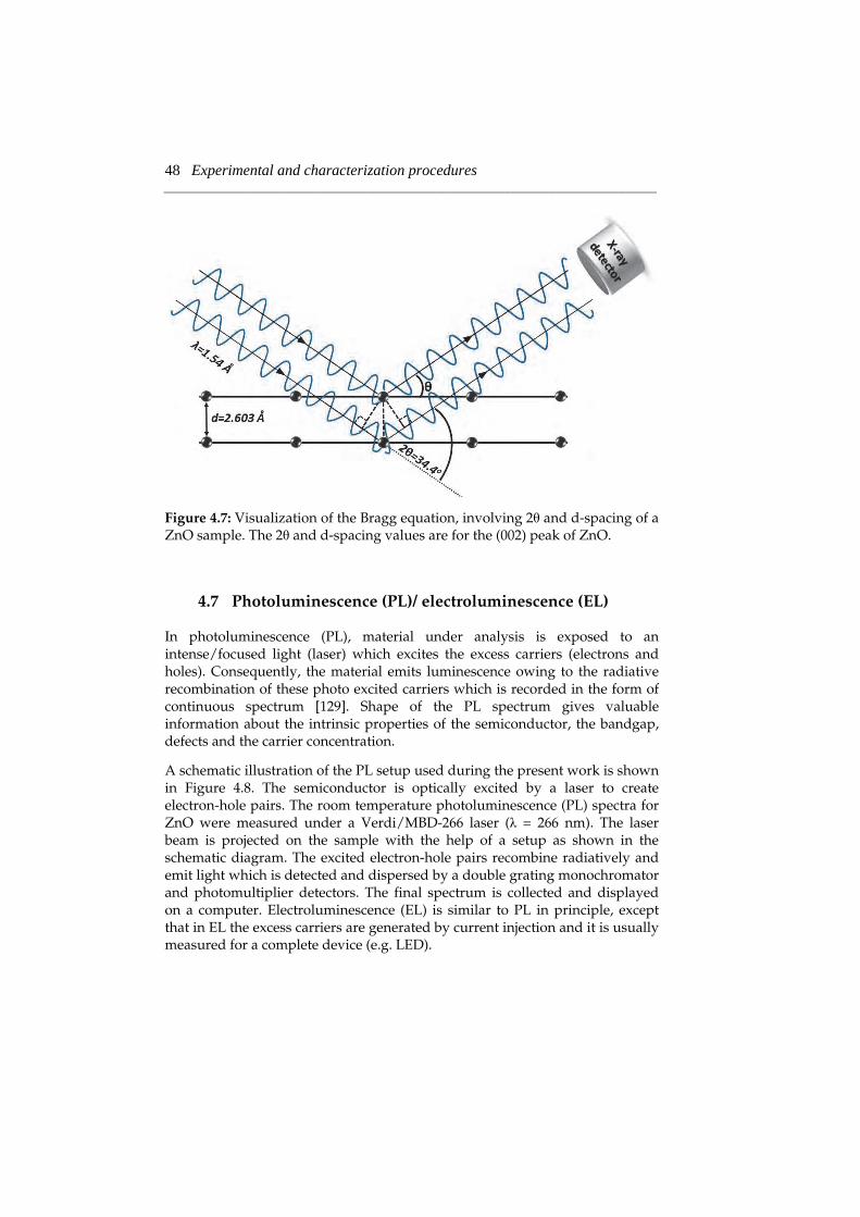
48 Experimental and characterization procedures ___________________________________________________________________________________________________
Figure 4.7: Visualization of the Bragg equation, involving 2 and d-spacing of a ZnO sample. The 2 and d-spacing values are for the (002) peak of ZnO.
4.7 Photoluminescence (PL)/ electroluminescence (EL)
In photoluminescence (PL), material under analysis is exposed to an intense/focused light (laser) which excites the excess carriers (electrons and holes). Consequently, the material emits luminescence owing to the radiative recombination of these photo excited carriers which is recorded in the form of continuous spectrum [129]. Shape of the PL spectrum gives valuable information about the intrinsic properties of the semiconductor, the bandgap, defects and the carrier concentration.
A schematic illustration of the PL setup used during the present work is shown in Figure 4.8. The semiconductor is optically excited by a laser to create electron-hole pairs. The room temperature photoluminescence (PL) spectra for ZnO were measured under a Verdi/MBD-266 laser ( = 266 nm). The laser beam is projected on the sample with the help of a setup as shown in the schematic diagram. The excited electron-hole pairs recombine radiatively and emit light which is detected and dispersed by a double grating monochromator and photomultiplier detectors. The final spectrum is collected and displayed on a computer. Electroluminescence (EL) is similar to PL in principle, except that in EL the excess carriers are generated by current injection and it is usually measured for a complete device (e.g. LED).
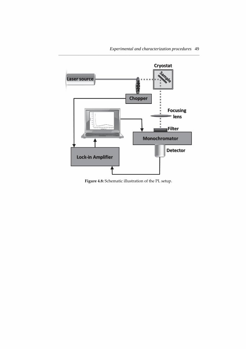
Experimental and characterization procedures 49 ___________________________________________________________________________________________________
Figure 4.8: Schematic illustration of the PL setup.

50 Experimental and characterization procedures ___________________________________________________________________________________________________
Results and Discussion 51 ___________________________________________________________________________________________________
C h a p t e r 5
Results and Discussion
Graphene and ZnO nanostructures were used to fabricate nano and optoelectronic devices, including field effect transistors (FETs), light emitting diodes (LEDs) and sensors. The junction between graphene and ZnO has also been characterized and reported. In this chapter, the experimental results of the junction analysis and the fabricated devices will be given and discussed.
5 5.1 Synthesis, basic devices and junction study
This section covers the results from paper 1-3. In paper 1, the functionalized graphene was synthesized chemically and stabilized in aqueous solutions by the assistance of a polycation (details of synthesis given in section 3.2.1.1). This aqueous dispersion of graphene was found to be stable even after 2 months, whereas the reduced GO without the addition of the polycation (PQ-16) formed agglomerates soon after reduction with hydrazine. The underlying mechanism has been associated with adsorption of some of the polycations on the surface of the graphene membranes by non-covalent - interactions between the imidazolium rings of the salt and graphene, soon after reduction with hydrazine monohydrate [130].
The graphene was deposited onto Si/SiO2 (SiO2 thickness ~300 nm) substrates by dip-coating and treated at 400 oC for 2 h in Ar/H2 to further reduce the graphene oxide and also to sublimate the solution residue. The optical microscope images were taken in order to identify graphene [131]. Atomic force microscope measurements were carried out to confirm the presence of single and few layer graphene by measuring step height [102]. Graphene shows typical wrinkled structure which is intrinsic to graphene [132] over relatively large sheet sizes. Very large graphene membranes with sizes around 10 ×10 μm were identified. The size was found to be directly related with sonication power and time. Excessive sonication results in very small graphene sheets whereas less sonication results in incomplete exfoliation of graphite oxide. The average thickness of a GO sheet was ~1 nm (Fig. 2), which in agreement with the preceding research, confirming that the graphite oxide was completely exfoliated. We observed heights from slightly less them 1nm to a few nm thick. We assigned the sheets with height ~1nm, ~1.5nm, ~2 nm and <5nm< to be 1, 2, 3, few layered GO sheets, respectively. This was in agreement with the reported AFM results on few-layer graphene sheets [2, 9, 133], where the single layer graphene is always ~1nm, probably due to different attraction force between AFM tips and graphene as compared to SiO2 and imperfect interface between graphene and SiO2. AFM image of our chemically reduced GO sheet after addition of PQ-16, deposited on SiO2/Si substrate by drop
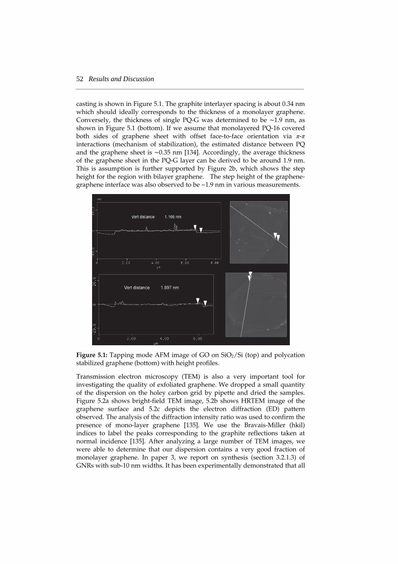
52 Results and Discussion ___________________________________________________________________________________________________
casting is shown in Figure 5.1. The graphite interlayer spacing is about 0.34 nm which should ideally corresponds to the thickness of a monolayer graphene. Conversely, the thickness of single PQ-G was determined to be 1.9 nm, as shown in Figure 5.1 (bottom). If we assume that monolayered PQ-16 covered both sides of graphene sheet with offset face-to-face orientation via - interactions (mechanism of stabilization), the estimated distance between PQ and the graphene sheet is 0.35 nm [134]. Accordingly, the average thickness of the graphene sheet in the PQ-G layer can be derived to be around 1.9 nm. This is assumption is further supported by Figure 2b, which shows the step height for the region with bilayer graphene. The step height of the graphene-graphene interface was also observed to be ~1.9 nm in various measurements.
Figure 5.1: Tapping mode AFM image of GO on SiO2/Si (top) and polycation stabilized graphene (bottom) with height profiles.
Transmission electron microscopy (TEM) is also a very important tool for investigating the quality of exfoliated graphene. We dropped a small quantity of the dispersion on the holey carbon grid by pipette and dried the samples. Figure 5.2a shows bright-field TEM image, 5.2b shows HRTEM image of the graphene surface and 5.2c depicts the electron diffraction (ED) pattern observed. The analysis of the diffraction intensity ratio was used to confirm the presence of mono-layer graphene [135]. We use the Bravais-Miller (hkil) indices to label the peaks corresponding to the graphite reflections taken at normal incidence [135]. After analyzing a large number of TEM images, we were able to determine that our dispersion contains a very good fraction of monolayer graphene. In paper 3, we report on synthesis (section 3.2.1.3) of GNRs with sub-10 nm widths. It has been experimentally demonstrated that all
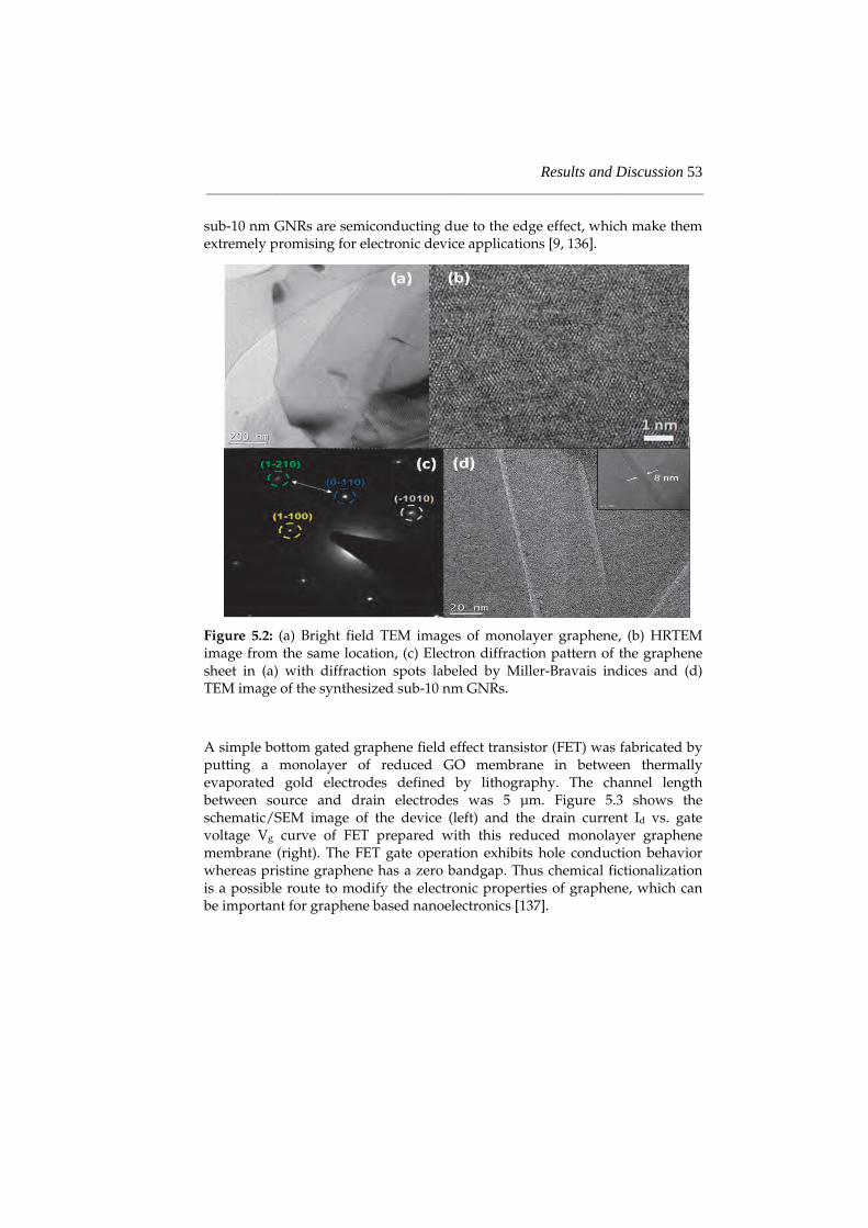
Results and Discussion 53 ___________________________________________________________________________________________________
sub-10 nm GNRs are semiconducting due to the edge effect, which make them extremely promising for electronic device applications [9, 136].
Figure 5.2: (a) Bright field TEM images of monolayer graphene, (b) HRTEM image from the same location, (c) Electron diffraction pattern of the graphene sheet in (a) with diffraction spots labeled by Miller-Bravais indices and (d) TEM image of the synthesized sub-10 nm GNRs.
A simple bottom gated graphene field effect transistor (FET) was fabricated by putting a monolayer of reduced GO membrane in between thermally evaporated gold electrodes defined by lithography. The channel length between source and drain electrodes was 5 μm. Figure 5.3 shows the schematic/SEM image of the device (left) and the drain current Id vs. gate voltage Vg curve of FET prepared with this reduced monolayer graphene membrane (right). The FET gate operation exhibits hole conduction behavior whereas pristine graphene has a zero bandgap. Thus chemical fictionalization is a possible route to modify the electronic properties of graphene, which can be important for graphene based nanoelectronics [137].
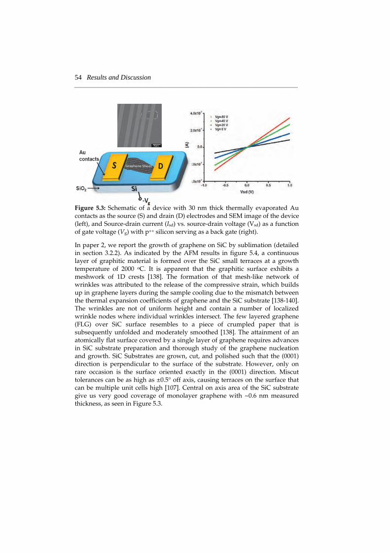
54 Results and Discussion ___________________________________________________________________________________________________
Figure 5.3: Schematic of a device with 30 nm thick thermally evaporated Au contacts as the source (S) and drain (D) electrodes and SEM image of the device (left), and Source-drain current (Isd) vs. source-drain voltage (Vsd) as a function of gate voltage (Vg) with p++ silicon serving as a back gate (right).
In paper 2, we report the growth of graphene on SiC by sublimation (detailed in section 3.2.2). As indicated by the AFM results in figure 5.4, a continuous layer of graphitic material is formed over the SiC small terraces at a growth temperature of 2000 oC. It is apparent that the graphitic surface exhibits a meshwork of 1D crests [138]. The formation of that mesh-like network of wrinkles was attributed to the release of the compressive strain, which builds up in graphene layers during the sample cooling due to the mismatch between the thermal expansion coefficients of graphene and the SiC substrate [138-140]. The wrinkles are not of uniform height and contain a number of localized wrinkle nodes where individual wrinkles intersect. The few layered graphene (FLG) over SiC surface resembles to a piece of crumpled paper that is subsequently unfolded and moderately smoothed [138]. The attainment of an atomically flat surface covered by a single layer of graphene requires advances in SiC substrate preparation and thorough study of the graphene nucleation and growth. SiC Substrates are grown, cut, and polished such that the (0001) direction is perpendicular to the surface of the substrate. However, only on rare occasion is the surface oriented exactly in the (0001) direction. Miscut tolerances can be as high as ±0.5° off axis, causing terraces on the surface that can be multiple unit cells high [107]. Central on axis area of the SiC substrate give us very good coverage of monolayer graphene with ~0.6 nm measured thickness, as seen in Figure 5.3.
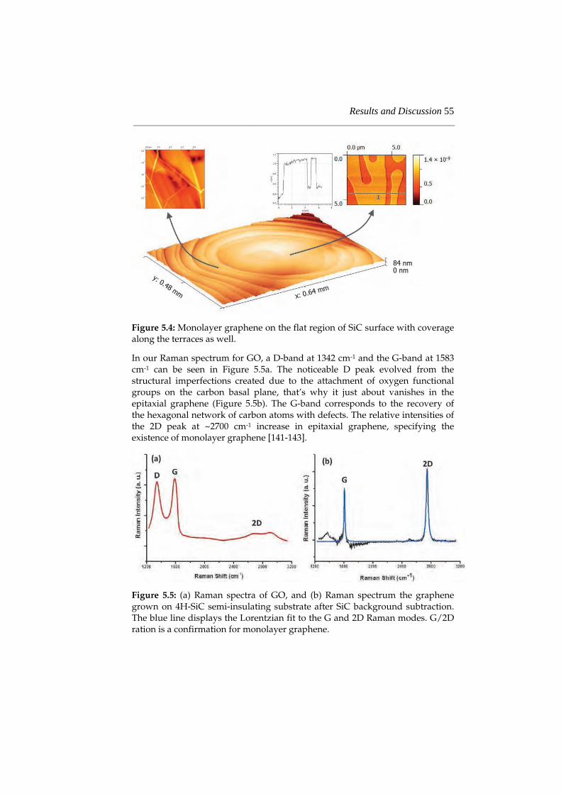
Results and Discussion 55 ___________________________________________________________________________________________________
Figure 5.4: Monolayer graphene on the flat region of SiC surface with coverage along the terraces as well.
In our Raman spectrum for GO, a D-band at 1342 cm-1 and the G-band at 1583 cm-1 can be seen in Figure 5.5a. The noticeable D peak evolved from the structural imperfections created due to the attachment of oxygen functional groups on the carbon basal plane, that’s why it just about vanishes in the epitaxial graphene (Figure 5.5b). The G-band corresponds to the recovery of the hexagonal network of carbon atoms with defects. The relative intensities of the 2D peak at ~2700 cm-1 increase in epitaxial graphene, specifying the existence of monolayer graphene [141-143].
Figure 5.5: (a) Raman spectra of GO, and (b) Raman spectrum the graphene grown on 4H-SiC semi-insulating substrate after SiC background subtraction. The blue line displays the Lorentzian fit to the G and 2D Raman modes. G/2D ration is a confirmation for monolayer graphene.

56 Results and Discussion ___________________________________________________________________________________________________
Samples produced by our optimized process have relatively smooth surfaces with a big central flat area with gradual large, flat substrate terraces that reach several micrometres in size and these continue towards the ends of the wafer in steps several times the height of the original substrate steps (Figure 5.6). The graphene attained on this surface now consists primarily of monolayer graphene, with narrow bilayer (and occasional trilayer) stripes at the terrace edges [144]. This trend was confirmed by the study of Raman spectra (Figure 5.6, right). The full width at half maximum (FWHM) of the G peak is also not effected by the number of layers. The number of layers for graphene is strongly related to the shape of the 2D peak. Monolayer graphene for instance has a single and sharp 2D peak with FWHM of 30-40 cm-1. Whereas, bilayer and trilayer graphene has relatively broader 2D feature with FWHM of ~60 cm-1 for the bilayer and ~70 cm-1 for the trilayer [145, 146]. The 2D peak position, increases monotonously to higher wavenumber with increasing layer number.
Figure 5.6: Development of the graphene during graphitization of Si-face SiC. The surface termination is mostly monolayer graphene with narrow stripes of bilayer and trilayer graphene near the upper edge of the substrate terraces [144] along with AFM image (top, left) of the terraces of our sample. On the right, the measured Raman spectra for the mono- bi- and trilayer graphene are depicted with their respective FWHM.
Then, we demonstrated the controlled growth of ZnO NWs on graphene surface by using a low temperature hydrothermal routine (section 3.3.1). The mechanical stability and electrical behavior of the junction was analyzed. ZnO NW growth was achieved on spin coated graphene along with the nearly
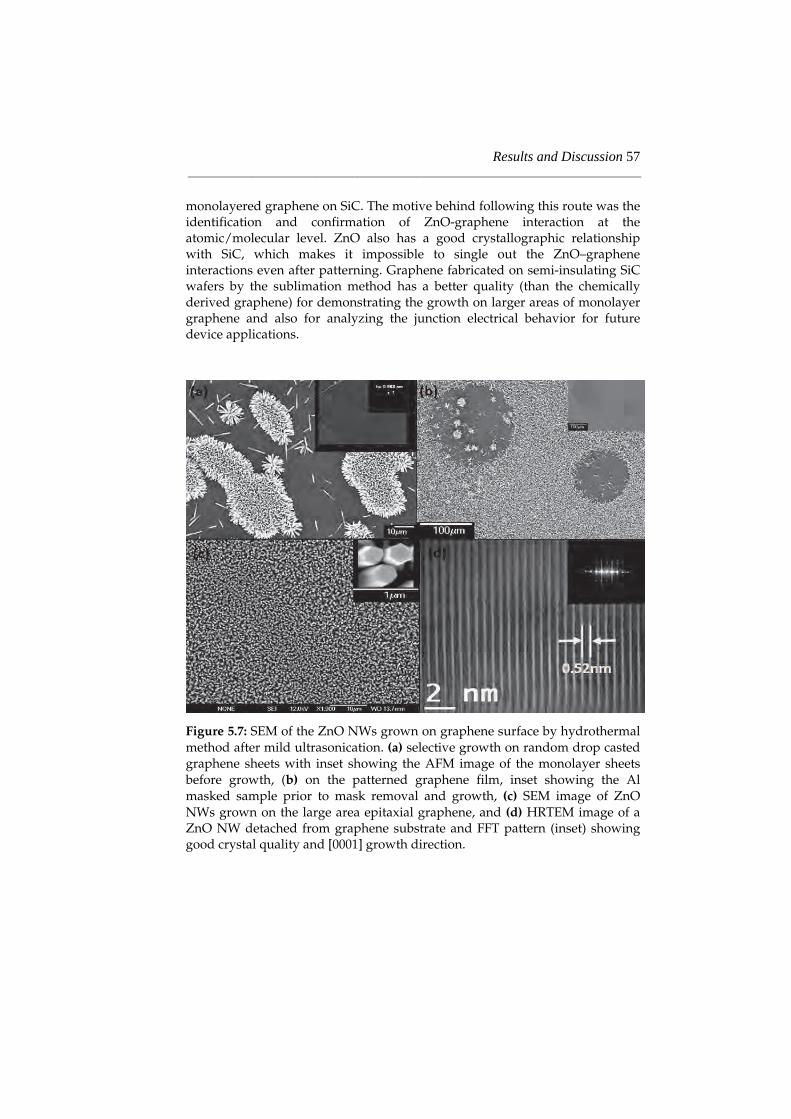
Results and Discussion 57 ___________________________________________________________________________________________________
monolayered graphene on SiC. The motive behind following this route was the identification and confirmation of ZnO-graphene interaction at the atomic/molecular level. ZnO also has a good crystallographic relationship with SiC, which makes it impossible to single out the ZnO–graphene interactions even after patterning. Graphene fabricated on semi-insulating SiC wafers by the sublimation method has a better quality (than the chemically derived graphene) for demonstrating the growth on larger areas of monolayer graphene and also for analyzing the junction electrical behavior for future device applications.
Figure 5.7: SEM of the ZnO NWs grown on graphene surface by hydrothermal method after mild ultrasonication. (a) selective growth on random drop casted graphene sheets with inset showing the AFM image of the monolayer sheets before growth, (b) on the patterned graphene film, inset showing the Al masked sample prior to mask removal and growth, (c) SEM image of ZnO NWs grown on the large area epitaxial graphene, and (d) HRTEM image of a ZnO NW detached from graphene substrate and FFT pattern (inset) showing good crystal quality and [0001] growth direction.
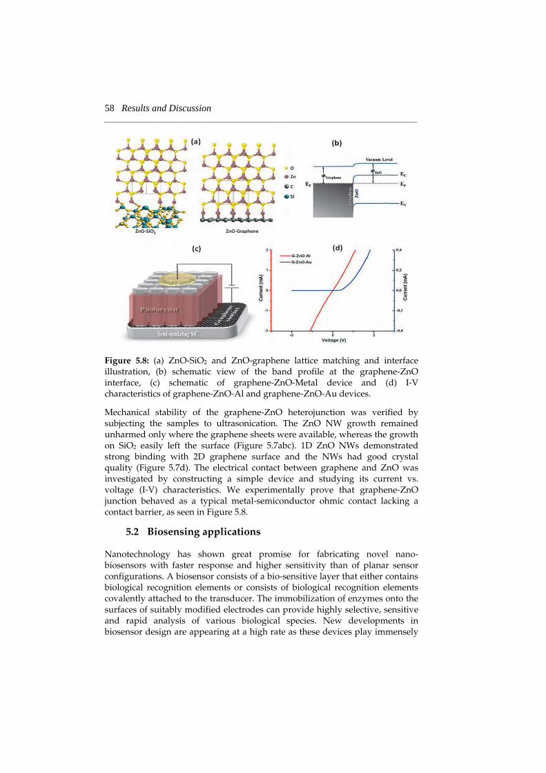
58 Results and Discussion ___________________________________________________________________________________________________
Figure 5.8: (a) ZnO-SiO2 and ZnO-graphene lattice matching and interface illustration, (b) schematic view of the band profile at the graphene-ZnO interface, (c) schematic of graphene-ZnO-Metal device and (d) I-V characteristics of graphene-ZnO-Al and graphene-ZnO-Au devices.
Mechanical stability of the graphene-ZnO heterojunction was verified by subjecting the samples to ultrasonication. The ZnO NW growth remained unharmed only where the graphene sheets were available, whereas the growth on SiO2 easily left the surface (Figure 5.7abc). 1D ZnO NWs demonstrated strong binding with 2D graphene surface and the NWs had good crystal quality (Figure 5.7d). The electrical contact between graphene and ZnO was investigated by constructing a simple device and studying its current vs. voltage (I-V) characteristics. We experimentally prove that graphene-ZnO junction behaved as a typical metal-semiconductor ohmic contact lacking a contact barrier, as seen in Figure 5.8.
5.2 Biosensing applications
Nanotechnology has shown great promise for fabricating novel nano-biosensors with faster response and higher sensitivity than of planar sensor configurations. A biosensor consists of a bio-sensitive layer that either contains biological recognition elements or consists of biological recognition elements covalently attached to the transducer. The immobilization of enzymes onto the surfaces of suitably modified electrodes can provide highly selective, sensitive and rapid analysis of various biological species. New developments in biosensor design are appearing at a high rate as these devices play immensely
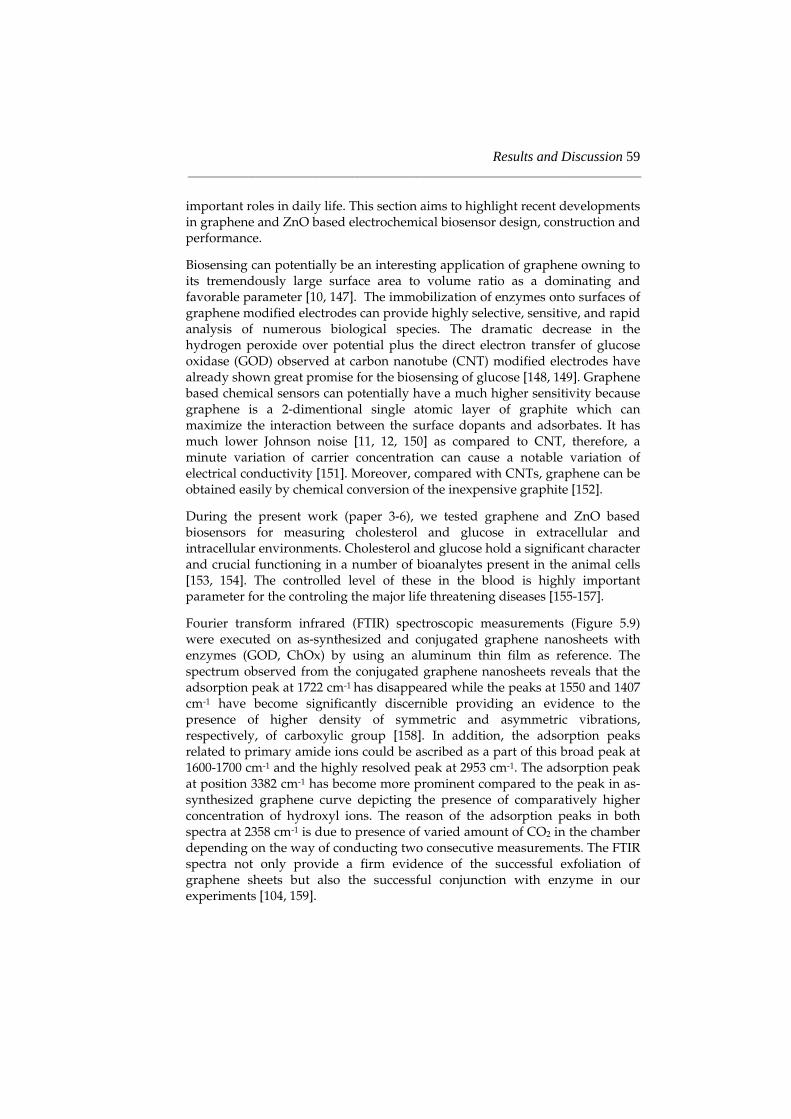
Results and Discussion 59 ___________________________________________________________________________________________________
important roles in daily life. This section aims to highlight recent developments in graphene and ZnO based electrochemical biosensor design, construction and performance.
Biosensing can potentially be an interesting application of graphene owning to its tremendously large surface area to volume ratio as a dominating and favorable parameter [10, 147]. The immobilization of enzymes onto surfaces of graphene modified electrodes can provide highly selective, sensitive, and rapid analysis of numerous biological species. The dramatic decrease in the hydrogen peroxide over potential plus the direct electron transfer of glucose oxidase (GOD) observed at carbon nanotube (CNT) modified electrodes have already shown great promise for the biosensing of glucose [148, 149]. Graphene based chemical sensors can potentially have a much higher sensitivity because graphene is a 2-dimentional single atomic layer of graphite which can maximize the interaction between the surface dopants and adsorbates. It has much lower Johnson noise [11, 12, 150] as compared to CNT, therefore, a minute variation of carrier concentration can cause a notable variation of electrical conductivity [151]. Moreover, compared with CNTs, graphene can be obtained easily by chemical conversion of the inexpensive graphite [152].
During the present work (paper 3-6), we tested graphene and ZnO based biosensors for measuring cholesterol and glucose in extracellular and intracellular environments. Cholesterol and glucose hold a significant character and crucial functioning in a number of bioanalytes present in the animal cells [153, 154]. The controlled level of these in the blood is highly important parameter for the controling the major life threatening diseases [155-157].
Fourier transform infrared (FTIR) spectroscopic measurements (Figure 5.9) were executed on as-synthesized and conjugated graphene nanosheets with enzymes (GOD, ChOx) by using an aluminum thin film as reference. The spectrum observed from the conjugated graphene nanosheets reveals that the adsorption peak at 1722 cm-1 has disappeared while the peaks at 1550 and 1407 cm-1 have become significantly discernible providing an evidence to the presence of higher density of symmetric and asymmetric vibrations, respectively, of carboxylic group [158]. In addition, the adsorption peaks related to primary amide ions could be ascribed as a part of this broad peak at 1600-1700 cm-1 and the highly resolved peak at 2953 cm-1. The adsorption peak at position 3382 cm-1 has become more prominent compared to the peak in as-synthesized graphene curve depicting the presence of comparatively higher concentration of hydroxyl ions. The reason of the adsorption peaks in both spectra at 2358 cm-1 is due to presence of varied amount of CO2 in the chamber depending on the way of conducting two consecutive measurements. The FTIR spectra not only provide a firm evidence of the successful exfoliation of graphene sheets but also the successful conjunction with enzyme in our experiments [104, 159].
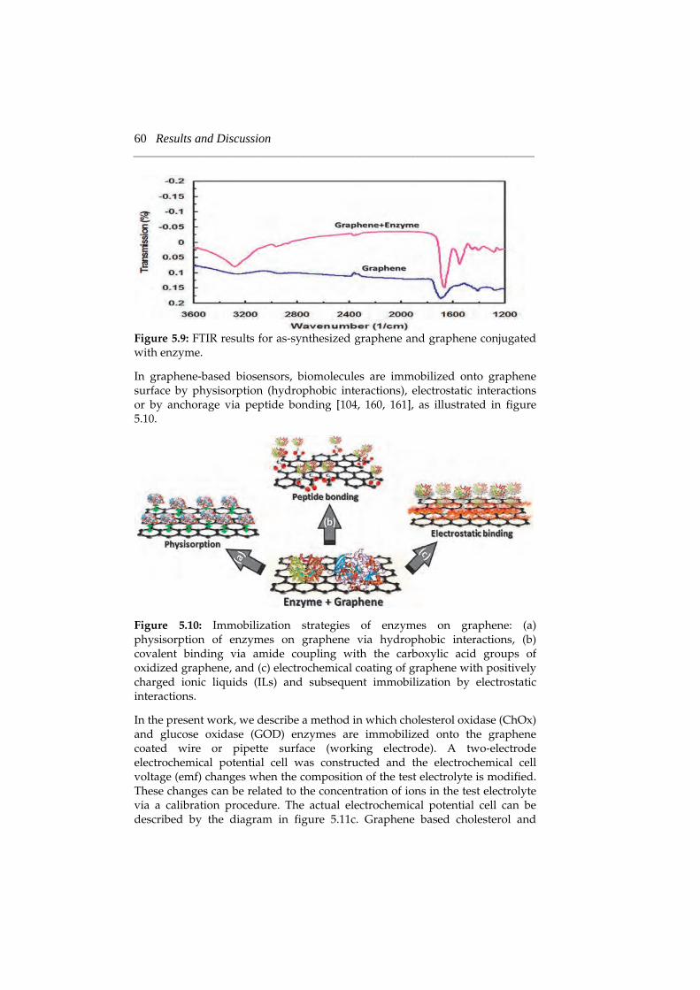
60 Results and Discussion ___________________________________________________________________________________________________
Figure 5.9: FTIR results for as-synthesized graphene and graphene conjugated with enzyme.
In graphene-based biosensors, biomolecules are immobilized onto graphene surface by physisorption (hydrophobic interactions), electrostatic interactions or by anchorage via peptide bonding [104, 160, 161], as illustrated in figure 5.10.
Figure 5.10: Immobilization strategies of enzymes on graphene: (a) physisorption of enzymes on graphene via hydrophobic interactions, (b) covalent binding via amide coupling with the carboxylic acid groups of oxidized graphene, and (c) electrochemical coating of graphene with positively charged ionic liquids (ILs) and subsequent immobilization by electrostatic interactions.
In the present work, we describe a method in which cholesterol oxidase (ChOx) and glucose oxidase (GOD) enzymes are immobilized onto the graphene coated wire or pipette surface (working electrode). A two-electrode electrochemical potential cell was constructed and the electrochemical cell voltage (emf) changes when the composition of the test electrolyte is modified. These changes can be related to the concentration of ions in the test electrolyte via a calibration procedure. The actual electrochemical potential cell can be described by the diagram in figure 5.11c. Graphene based cholesterol and
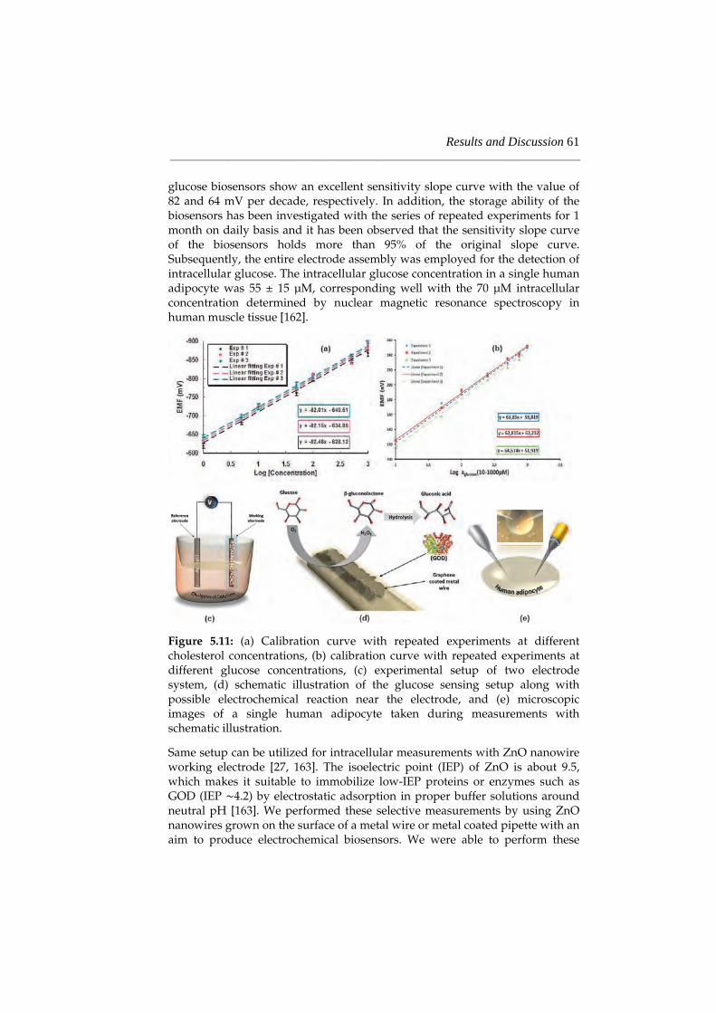
Results and Discussion 61 ___________________________________________________________________________________________________
glucose biosensors show an excellent sensitivity slope curve with the value of 82 and 64 mV per decade, respectively. In addition, the storage ability of the biosensors has been investigated with the series of repeated experiments for 1 month on daily basis and it has been observed that the sensitivity slope curve of the biosensors holds more than 95% of the original slope curve. Subsequently, the entire electrode assembly was employed for the detection of intracellular glucose. The intracellular glucose concentration in a single human adipocyte was 55 ± 15 μM, corresponding well with the 70 μM intracellular concentration determined by nuclear magnetic resonance spectroscopy in human muscle tissue [162].
Figure 5.11: (a) Calibration curve with repeated experiments at different cholesterol concentrations, (b) calibration curve with repeated experiments at different glucose concentrations, (c) experimental setup of two electrode system, (d) schematic illustration of the glucose sensing setup along with possible electrochemical reaction near the electrode, and (e) microscopic images of a single human adipocyte taken during measurements with schematic illustration.
Same setup can be utilized for intracellular measurements with ZnO nanowire working electrode [27, 163]. The isoelectric point (IEP) of ZnO is about 9.5, which makes it suitable to immobilize low-IEP proteins or enzymes such as GOD (IEP 4.2) by electrostatic adsorption in proper buffer solutions around neutral pH [163]. We performed these selective measurements by using ZnO nanowires grown on the surface of a metal wire or metal coated pipette with an aim to produce electrochemical biosensors. We were able to perform these
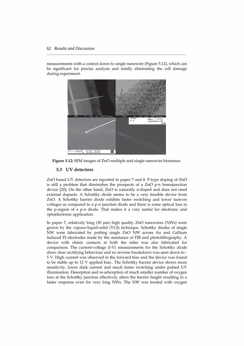
62 Results and Discussion ___________________________________________________________________________________________________
measurements with a control down to single nanowire (Figure 5.12), which can be significant for precise analysis and totally eliminating the cell damage during experiment.
Figure 5.12: SEM images of ZnO multiple and single nanowire biosensor.
5.3 UV detectors
ZnO based UV detectors are reported in paper 7 and 8. P-type doping of ZnO is still a problem that diminishes the prospects of a ZnO p-n homojunction device [20]. On the other hand, ZnO is naturally n-doped and does not need external dopants. A Schottky diode seems to be a very feasible device from ZnO. A Schottky barrier diode exhibits faster switching and lower turn-on voltages as compared to a p-n junction diode and there is some optical loss in the p-region of a p-n diode. That makes it a very useful for electronic and optoelectronic application.
In paper 7, relatively long (30 μm) high quality ZnO nanowires (NWs) were grown by the vapour-liquid-solid (VLS) technique. Schottky diodes of single NW were fabricated by putting single ZnO NW across Au and Gallium induced Pt electrodes made by the assistance of FIB and photolithography. A device with ohmic contacts at both the sides was also fabricated for comparison. The current-voltage (I-V) measurements for the Schottky diode show clear rectifying behaviour and no reverse breakdown was seen down to -5 V. High current was observed in the forward bias and the device was found to be stable up to 12 V applied bias.. The Schottky barrier device shows more sensitivity, lower dark current and much faster switching under pulsed UV illumination. Desorption and re-adsorption of much smaller number of oxygen ions at the Schottky junction effectively alters the barrier height resulting in a faster response even for very long NWs. The NW was treated with oxygen
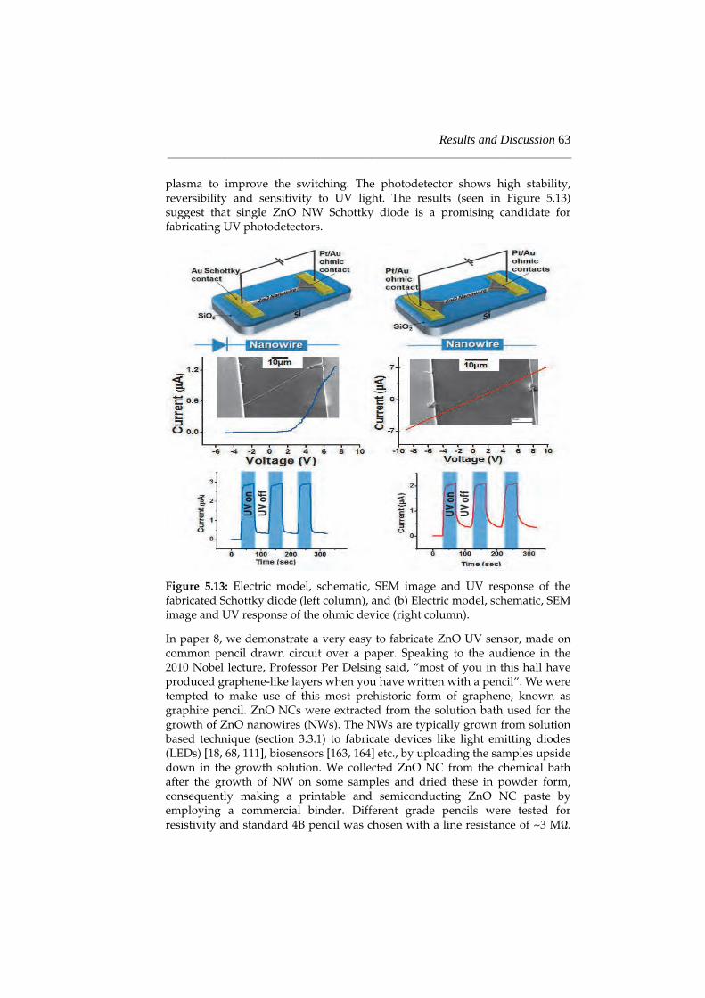
Results and Discussion 63 ___________________________________________________________________________________________________
plasma to improve the switching. The photodetector shows high stability, reversibility and sensitivity to UV light. The results (seen in Figure 5.13) suggest that single ZnO NW Schottky diode is a promising candidate for fabricating UV photodetectors.
Figure 5.13: Electric model, schematic, SEM image and UV response of the fabricated Schottky diode (left column), and (b) Electric model, schematic, SEM image and UV response of the ohmic device (right column).
In paper 8, we demonstrate a very easy to fabricate ZnO UV sensor, made on common pencil drawn circuit over a paper. Speaking to the audience in the 2010 Nobel lecture, Professor Per Delsing said, “most of you in this hall have produced graphene-like layers when you have written with a pencil”. We were tempted to make use of this most prehistoric form of graphene, known as graphite pencil. ZnO NCs were extracted from the solution bath used for the growth of ZnO nanowires (NWs). The NWs are typically grown from solution based technique (section 3.3.1) to fabricate devices like light emitting diodes (LEDs) [18, 68, 111], biosensors [163, 164] etc., by uploading the samples upside down in the growth solution. We collected ZnO NC from the chemical bath after the growth of NW on some samples and dried these in powder form, consequently making a printable and semiconducting ZnO NC paste by employing a commercial binder. Different grade pencils were tested for resistivity and standard 4B pencil was chosen with a line resistance of ~3 M .
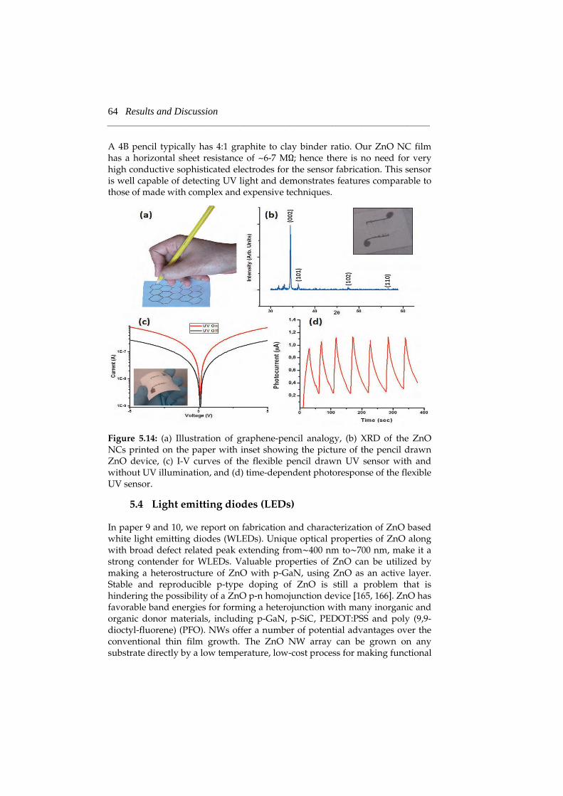
64 Results and Discussion ___________________________________________________________________________________________________
A 4B pencil typically has 4:1 graphite to clay binder ratio. Our ZnO NC film has a horizontal sheet resistance of ~6-7 M ; hence there is no need for very high conductive sophisticated electrodes for the sensor fabrication. This sensor is well capable of detecting UV light and demonstrates features comparable to those of made with complex and expensive techniques.
Figure 5.14: (a) Illustration of graphene-pencil analogy, (b) XRD of the ZnO NCs printed on the paper with inset showing the picture of the pencil drawn ZnO device, (c) I-V curves of the flexible pencil drawn UV sensor with and without UV illumination, and (d) time-dependent photoresponse of the flexible UV sensor.
5.4 Light emitting diodes (LEDs)
In paper 9 and 10, we report on fabrication and characterization of ZnO based white light emitting diodes (WLEDs). Unique optical properties of ZnO along with broad defect related peak extending from 400 nm to 700 nm, make it a strong contender for WLEDs. Valuable properties of ZnO can be utilized by making a heterostructure of ZnO with p-GaN, using ZnO as an active layer. Stable and reproducible p-type doping of ZnO is still a problem that is hindering the possibility of a ZnO p-n homojunction device [165, 166]. ZnO has favorable band energies for forming a heterojunction with many inorganic and organic donor materials, including p-GaN, p-SiC, PEDOT:PSS and poly (9,9-dioctyl-fluorene) (PFO). NWs offer a number of potential advantages over the conventional thin film growth. The ZnO NW array can be grown on any substrate directly by a low temperature, low-cost process for making functional
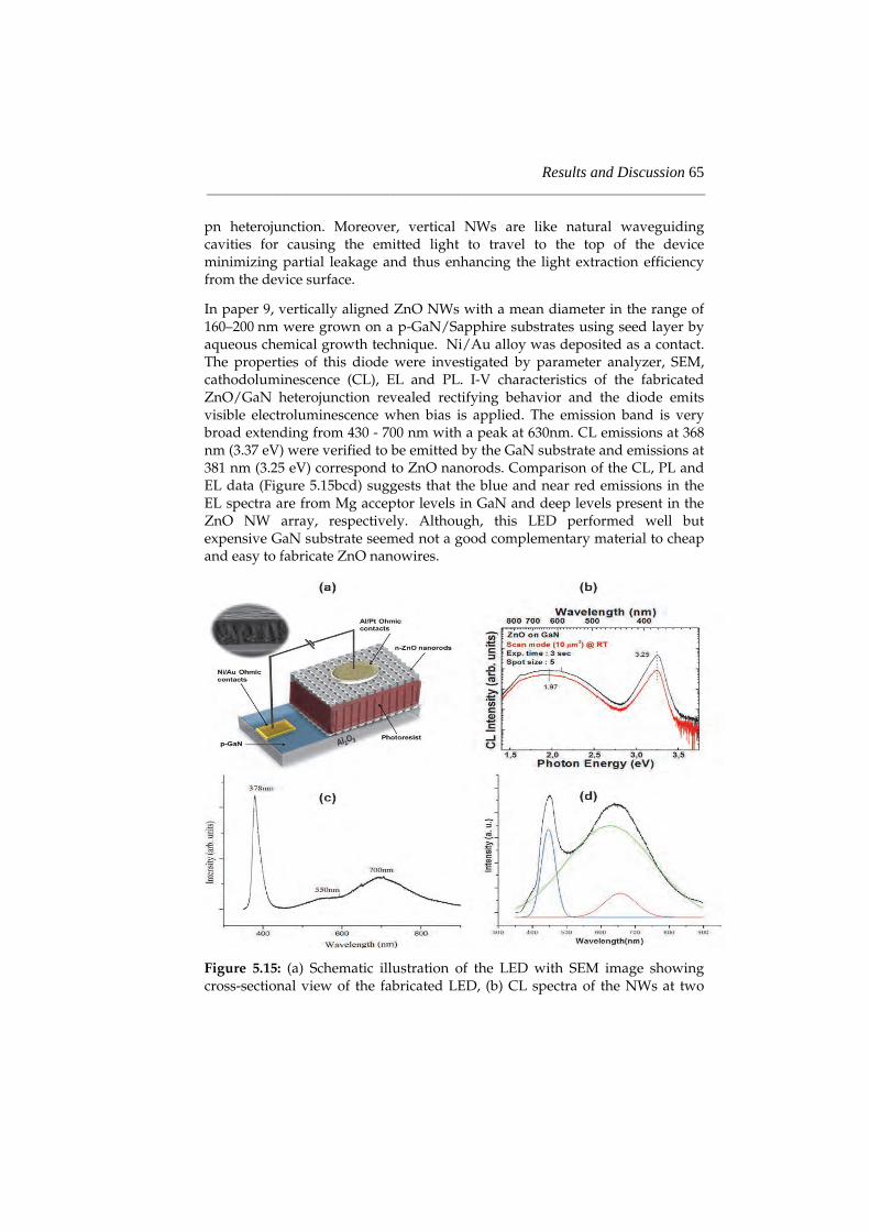
Results and Discussion 65 ___________________________________________________________________________________________________
pn heterojunction. Moreover, vertical NWs are like natural waveguiding cavities for causing the emitted light to travel to the top of the device minimizing partial leakage and thus enhancing the light extraction efficiency from the device surface.
In paper 9, vertically aligned ZnO NWs with a mean diameter in the range of 160–200 nm were grown on a p-GaN/Sapphire substrates using seed layer by aqueous chemical growth technique. Ni/Au alloy was deposited as a contact. The properties of this diode were investigated by parameter analyzer, SEM, cathodoluminescence (CL), EL and PL. I-V characteristics of the fabricated ZnO/GaN heterojunction revealed rectifying behavior and the diode emits visible electroluminescence when bias is applied. The emission band is very broad extending from 430 - 700 nm with a peak at 630nm. CL emissions at 368 nm (3.37 eV) were verified to be emitted by the GaN substrate and emissions at 381 nm (3.25 eV) correspond to ZnO nanorods. Comparison of the CL, PL and EL data (Figure 5.15bcd) suggests that the blue and near red emissions in the EL spectra are from Mg acceptor levels in GaN and deep levels present in the ZnO NW array, respectively. Although, this LED performed well but expensive GaN substrate seemed not a good complementary material to cheap and easy to fabricate ZnO nanowires.
Figure 5.15: (a) Schematic illustration of the LED with SEM image showing cross-sectional view of the fabricated LED, (b) CL spectra of the NWs at two
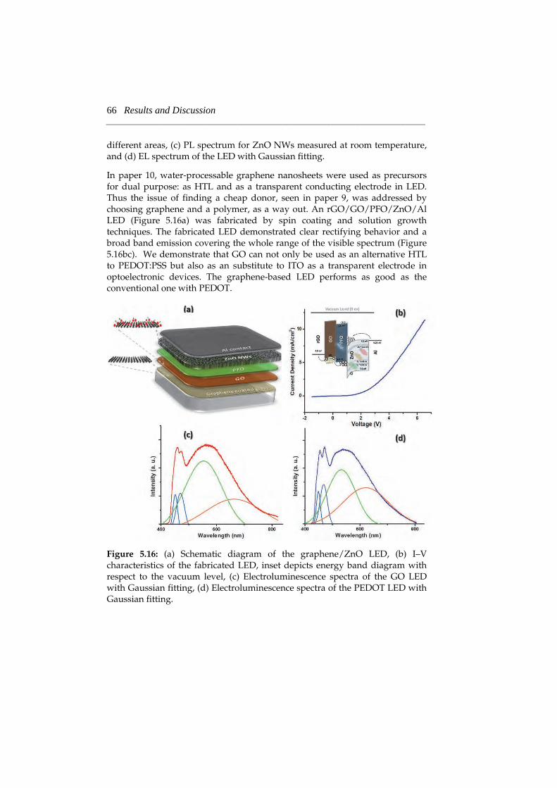
66 Results and Discussion ___________________________________________________________________________________________________
different areas, (c) PL spectrum for ZnO NWs measured at room temperature, and (d) EL spectrum of the LED with Gaussian fitting.
In paper 10, water-processable graphene nanosheets were used as precursors for dual purpose: as HTL and as a transparent conducting electrode in LED. Thus the issue of finding a cheap donor, seen in paper 9, was addressed by choosing graphene and a polymer, as a way out. An rGO/GO/PFO/ZnO/Al LED (Figure 5.16a) was fabricated by spin coating and solution growth techniques. The fabricated LED demonstrated clear rectifying behavior and a broad band emission covering the whole range of the visible spectrum (Figure 5.16bc). We demonstrate that GO can not only be used as an alternative HTL to PEDOT:PSS but also as an substitute to ITO as a transparent electrode in optoelectronic devices. The graphene-based LED performs as good as the conventional one with PEDOT.
Figure 5.16: (a) Schematic diagram of the graphene/ZnO LED, (b) I–V characteristics of the fabricated LED, inset depicts energy band diagram with respect to the vacuum level, (c) Electroluminescence spectra of the GO LED with Gaussian fitting, (d) Electroluminescence spectra of the PEDOT LED with Gaussian fitting.
Conclusions and Outlook 67 ___________________________________________________________________________________________________
C h a p t e r 6
6 Conclusions and Outlook
The present work mainly covers graphene and ZnO nanostructures, study of their growth mechanism by different techniques as well as junction study and application of their various combinations. This work can mainly be divided in two parts: (i) Synthesis, basic devices and junction study of graphene and ZnO nanostructures, (ii) Applications.
6.1 Summary
In the first part, the functionalized graphene was synthesized chemically and stabilized in aqueous solutions by the assistance of a polycation. This aqueous graphene dispersion was found to be stable even after 2 months, whereas the reduced GO without the addition of the polycation (PQ-16) formed agglomerates soon after reduction with hydrazine. The core mechanism has been associated with adsorption of some of the polycations on the surface of the graphene membranes by non-covalent - interactions between the imidazolium rings of the salt and graphene, soon after reduction with hydrazine monohydrate. A simple bottom gated graphene field effect transistor (FET) was fabricated to study the effect of chemical functionalization on the electronic properties of graphene. Then, growth of graphene on SiC by sublimation was performed and optimized. A very good coverage of monolayer graphene layer over 2 SiC wafer was attained at growth temperatures up to 1800 oC inside a HTCVD reactor. Then, we demonstrated the controlled growth of ZnO NWs on graphene surface by using a low temperature hydrothermal method. The mechanical stability and electrical behavior of the junction was analyzed. ZnO NWs demonstrated good mechanical stability with graphene due to good mutual crystallographic relationship. The graphene-ZnO junction behaved as a typical metal-semiconductor ohmic contact lacking a contact barrier.
In the second part, we demonstrated applications of graphene and ZnO nanostructures and their various combinations. Biosensing was found to be an interesting application of these nanomaterials owning to their exceptionally large surface area to volume ratio and biocompatibility. The immobilization of enzymes onto the surfaces of suitably modified electrodes provided highly selective, sensitive and rapid analysis of glucose and cholesterol. UV detection was also experimentally confirmed to be an interesting application. The
68 Conclusions and Outlook ___________________________________________________________________________________________________
photodetector shows high stability, reversibility and sensitivity to UV light. The results suggest that ZnO is a promising candidate for fabricating UV photodetectors. Single NW photodetectors were fabricated and their performance was optimised by making good Schottky contacts and oxygen plasma treatment. We also demonstrated a novel type of UV sensors by making use of the most prehistoric form of graphene, known as graphite pencil. ZnO NCs were extracted from the solution bath used for the growth of ZnO NWs and screen printed onto the pencil drawn circuitry. This sensor was found to be well capable of detecting UV light and displayed features comparable to those of made with complex and expensive techniques. Lastly, we report on fabrication and characterization of ZnO based WLEDs as unique optical properties of ZnO along with broad defect related peak making it a strong contender for WLEDs. First, we fabricated ZnO/GaN heterojunction LED which emitted good observable white electroluminescence on bias application. Then in the second type of LED, water-processable graphene nanosheets were used as precursors for dual purpose: as HTL and as a transparent conducting electrode in LED. Thus the issue of finding a cheap donor, seen in ZnO/GaN heterojunction LED, was addressed by choosing graphene and a polymer as a solution. An rGO/GO/PFO/ZnO/Al LED was fabricated by spin coating and solution growth techniques. The fabricated LED demonstrated clear rectifying behavior and a broad band emission covering the whole range of the visible spectrum.
6.2 Future Outlook
With all the recent and well justified boom in graphene research, many critical issues are still to be resolved before bringing out the all-graphene electronics into the market. We have experimentally seen that the interaction between graphene and SiC substrate are critical to the future applications of epitaxial graphene. Besides that, graphene can be seen as a perfect replacement for ITO as transparent conducting displays. Better control and optimization of functionalization of graphene can open new ways for a diverse range of applications. Similarly, a diverse range of ZnO nanostructures can find application in many applications such as LEDs, biosensors, UV sensors, nano-generators etc. The novel design of having very few or even a single ZnO NW on the sharp tip makes it possible to penetrate the cell membrane with nanosensor devices and measure biological species in living cells. The amalgamation of the exceptional properties of graphene with good semiconducting properties of ZnO can lead the way towards the realization of future devices.
References 69 ___________________________________________________________________________________________________
References
[1] C. Ltd, "Global Funding Of Nanotechnologies & Its Impact," Madrid 2011. [2] K. S. Novoselov, A. K. Geim, S. V. Morozov, D. Jiang, Y. Zhang, S. V.
Dubonos, I. V. Grigorieva, and A. A. Firsov, "Electric Field Effect in Atomically Thin Carbon Films," Science, vol. 306, pp. 666-669, October 22, 2004 2004.
[3] A. A. Balandin, S. Ghosh, W. Bao, I. Calizo, D. Teweldebrhan, F. Miao, and C. N. Lau, "Superior Thermal Conductivity of Single-Layer Graphene," Nano Letters, vol. 8, pp. 902-907, 2008.
[4] K. I. Bolotin, K. J. Sikes, Z. Jiang, M. Klima, G. Fudenberg, J. Hone, P. Kim, and H. L. Stormer, "Ultrahigh electron mobility in suspended graphene," Solid State Communications, vol. 146, pp. 351-355, 2008.
[5] H. Chen, M. B. Muller, K. J. Gilmore, G. G. Wallace, and D. Li, "Mechanically strong, electrically conductive, and biocompatible graphene paper," Adv. Mater., vol. 20, p. 3557, Sep 17 2008.
[6] X. Du, I. Skachko, A. Barker, and E. Y. Andrei, "Approaching ballistic transport in suspended graphene," Nat. Nanotech., vol. 3, pp. 491-495, Aug 2008.
[7] M. Freitag, H. Y. Chiu, M. Steiner, V. Perebeinos, and P. Avouris, "Thermal infrared emission from biased graphene," Nat. Nanotech., vol. 5, pp. 497-501, Jul 2010.
[8] S. Garaj, W. Hubbard, A. Reina, J. Kong, D. Branton, and J. A. Golovchenko, "Graphene as a subnanometre trans-electrode membrane," Nature, vol. 467, pp. 190-U73, Sep 9 2010.
[9] X. Li, X. Wang, L. Zhang, S. Lee, and H. Dai, "Chemically Derived, Ultrasmooth Graphene Nanoribbon Semiconductors," Science, vol. 319, pp. 1229-1232, February 29, 2008 2008.
[10] M. D. Stoller, S. J. Park, Y. W. Zhu, J. H. An, and R. S. Ruoff, "Graphene-Based Ultracapacitors," Nano Lett., vol. 8, pp. 3498-3502, Oct 2008.
[11] A. K. Geim and K. S. Novoselov, "The rise of graphene," Nat Mater, vol. 6, pp. 183-191, 2007.
[12] K. S. Novoselov, A. K. Geim, S. V. Morozov, D. Jiang, M. I. Katsnelson, I. V. Grigorieva, S. V. Dubonos, and A. A. Firsov, "Two-dimensional gas of massless Dirac fermions in graphene," Nature, vol. 438, pp. 197-200, 2005.
[13] Y. Zhang, Y. W. Tan, H. L. Stormer, and P. Kim, "Experimental observation of the quantum Hall effect and Berry's phase in graphene," Nature, vol. 438, pp. 201-204, 2005.
[14] W. Zhong Lin, "Nanostructures of zinc oxide," Materials Today, vol. 7, pp. 26-33, 2004.
[15] M. Willander, L. L. Yang, A. Wadeasa, S. U. Ali, M. H. Asif, Q. X. Zhao, and O. Nur, "Zinc oxide nanowires: controlled low temperature growth and some electrochemical and optical nano-devices," Journal of Materials Chemistry, vol. 19, pp. 1006-1018, 2009.
70 References ___________________________________________________________________________________________________
[16] S. Kishwar, K. ul Hasan, G. Tzamalis, O. Nur, M. Willander, H. S. Kwack, and D. L. S. Dang, "Electro-optical and cathodoluminescence properties of low temperature grown ZnO nanorods/p-GaN white light emitting diodes," physica status solidi (a), vol. 9999, p. NA, 2009.
[17] J. M. a. A. M. A. van Dijken, "The influence of particle size on the luminescence quantum efficiency of nanocrystalline ZnO particles " Journal of Luminescence, vol. 92, pp. 323-328 2001.
[18] N. Alvi, K. ul Hasan, O. Nur, and M. Willander, "The origin of the red emission in n-ZnO nanotubes/p-GaN white light emitting diodes," Nanoscale Research Letters, vol. 6, p. 130, 2011.
[19] H. C. Chen, M. J. Chen, Y. H. Huang, W. C. Sun, W. C. Li, J. R. Yang, H. Kuan, and M. Shiojiri, "White-Light Electroluminescence From n-ZnO/p-GaN Heterojunction Light-Emitting Diodes at Reverse Breakdown Bias," Electron Devices, IEEE Transactions on, vol. 58, pp. 3970-3975, 2011.
[20] H. Soon-Ku, H. Takashi, M. Hisao, C. Yefan, K. Hang-Ju, Y. Takafumi, T. Akinori, S. Hiroyuki, and S. Shigeru, "Band alignment at a ZnO/GaN (0001) heterointerface," Applied Physics Letters, vol. 78, pp. 3349-3351, 2001.
[21] K. S. Novoselov, D. Jiang, F. Schedin, T. J. Booth, V. V. Khotkevich, S. V. Morozov, and A. K. Geim, "Two-dimensional atomic crystals," Proceedings of the National Academy of Sciences of the United States of America, vol. 102, pp. 10451-10453, July 26, 2005 2005.
[22] N. D. Mermin, "Crystalline Order in Two Dimensions," Physical Review, vol. 176, pp. 250-254, 1968.
[23] A. Fasolino, J. H. Los, and M. I. Katsnelson, "Intrinsic ripples in graphene," Nat Mater, vol. 6, pp. 858-861, 2007.
[24] J. C. Meyer, A. K. Geim, M. I. Katsnelson, K. S. Novoselov, T. J. Booth, and S. Roth, "The structure of suspended graphene sheets," Nature, vol. 446, pp. 60-63, 2007.
[25] M. Fujita, K. Wakabayashi, K. Nakada, and K. Kusakabe, "Peculiar Localized State at Zigzag Graphite Edge," Journal of the Physical Society of Japan, vol. 65, p. 1920, 1996.
[26] K. Nakada, M. Fujita, G. Dresselhaus, and M. S. Dresselhaus, "Edge state in graphene ribbons: Nanometer size effect and edge shape dependence," Physical Review B, vol. 54, pp. 17954-17961, 1996.
[27] M. Willander, K. ul Hasan, O. Nur, A. Zainelabdin, S. Zaman, and G. Amin, "Recent progress on growth and device development of ZnO and CuO nanostructures and graphene nanosheets," Journal of Materials Chemistry, vol. 22, 2012.
[28] G. Dobrik, L. Tapasztó, P. Nemes-Incze, P. Lambin, and L. P. Biró, "Crystallographically oriented high resolution lithography of graphene nanoribbons by STM lithography," physica status solidi (b), vol. 247, pp. 896-902, 2010.
[29] L. Chuanxin, K. Tahy, F. Tian, L. Guowang, H. G. Xing, and D. Jena, "Quantum transport in patterned graphene nanoribbons," in
References 71 ___________________________________________________________________________________________________
Semiconductor Device Research Symposium, 2009. ISDRS '09. International, 2009, pp. 1-2.
[30] A. V. Talyzin, I. V. Anoshkin, A. V. Krasheninnikov, R. M. Nieminen, A. G. Nasibulin, H. Jiang, and E. I. Kauppinen, "Synthesis of Graphene Nanoribbons Encapsulated in Single-Walled Carbon Nanotubes," Nano Letters, vol. 11, pp. 4352-4356, 2012/03/02 2011.
[31] O. O. Kit, T. Tallinen, L. Mahadevan, J. Timonen, and P. Koskinen, "Twisting graphene nanoribbons into carbon nanotubes," Physical Review B, vol. 85, p. 085428, 2012.
[32] A. H. Castro Neto, F. Guinea, N. M. R. Peres, K. S. Novoselov, and A. K. Geim, "The electronic properties of graphene," Reviews of Modern Physics, vol. 81, pp. 109-162, 2009.
[33] P. Dietl, "Numerical Studies of Electronic Transport through Graphene Nanoribbons with Disorder." vol. Diploma Karlsruhe: University of Karlsruhe, 2009, p. 76.
[34] P. R. Wallace, "The Band Theory of Graphite," Physical Review, vol. 71, pp. 622-634, 1947.
[35] S. Konschuh, M. Gmitra, and J. Fabian, "Tight-binding theory of the spin-orbit coupling in graphene," Physical Review B, vol. 82, p. 245412, 2010.
[36] D. R. Cooper, B. D'Anjou, N. Ghattamaneni, B. Harack, M. Hilke, A. Horth, N. Majlis, M. Massicotte, L. Vandsburger, E. Whiteway, and V. Yu, "Experimental review of graphene," ArXiv e-prints, vol. 1110.6557, 2011.
[37] M. I. Katsnelson, "Graphene: carbon in two dimensions," eprint arXiv:cond-mat/0612534, 2006.
[38] M. I. Katsnelson, K. S. Novoselov, and A. K. Geim, "Chiral tunnelling and the Klein paradox in graphene," Nat Phys, vol. 2, pp. 620-625, 2006.
[39] A. F. Young and P. Kim, "Quantum interference and Klein tunnelling in graphene heterojunctions," Nat Phys, vol. 5, pp. 222-226, 2009.
[40] N. Stander, B. Huard, and D. Goldhaber-Gordon, "Evidence for Klein Tunneling in Graphene p-n Junctions," Physical Review Letters, vol. 102, p. 026807, 2009.
[41] H. Shioya, M. Yamamoto, S. Russo, M. F. Craciun, and S. Tarucha, "Gate tunable non-linear currents in bilayer graphene diodes," Applied Physics Letters, vol. 100, pp. 033113-4, 2012.
[42] Y. Zhang, T. T. Tang, C. Girit, Z. Hao, M. C. Martin, A. Zettl, M. F. Crommie, Y. R. Shen, and F. Wang, "Direct observation of a widely tunable bandgap in bilayer graphene," Nature, vol. 459, pp. 820-823, 2009.
[43] R. R. Nair, P. Blake, A. N. Grigorenko, K. S. Novoselov, T. J. Booth, T. Stauber, N. M. R. Peres, and A. K. Geim, "Fine Structure Constant Defines Visual Transparency of Graphene," Science, vol. 320, p. 1308, June 6, 2008 2008.
[44] T. Fang, A. Konar, H. Xing, and D. Jena, "Carrier statistics and quantum capacitance of graphene sheets and ribbons," Applied Physics Letters, vol. 91, pp. 092109-3, 2007.
72 References ___________________________________________________________________________________________________
[45] J. Wu, M. Agrawal, H. c. A. Becerril, Z. Bao, Z. Liu, Y. Chen, and P. Peumans, "Organic Light-Emitting Diodes on Solution-Processed Graphene Transparent Electrodes," ACS Nano, vol. 4, pp. 43-48, 2011/11/16 2009.
[46] H. M. Dong, W. Xu, J. Zhang, and Y.-z. Yuan, "Terahertz absorption window and high transmission in graphene bilayer," Optics Communications, vol. 283, pp. 3695-3697, 2010.
[47] J. M. Dawlaty, S. Shivaraman, J. Strait, P. George, M. Chandrashekhar, F. Rana, M. G. Spencer, D. Veksler, and Y. Chen, "Measurement of the optical absorption spectra of epitaxial graphene from terahertz to visible," Applied Physics Letters, vol. 93, pp. 131905-3, 2008.
[48] A. Vadym and Z. Vladimir, "Phonons in graphene with point defects," Journal of Physics: Condensed Matter, vol. 23, p. 015402, 2011.
[49] J. C. Charlier, P. Eklund, J. Zhu, and A. Ferrari, "Electron and Phonon Properties of Graphene: Their Relationship with Carbon Nanotubes
Carbon Nanotubes." vol. 111: Springer Berlin / Heidelberg, 2008, pp. 673-709. [50] M. S. Dresselhaus, G. Dresselhaus, R. Saito, and A. Jorio, "Raman
spectroscopy of carbon nanotubes," Physics Reports, vol. 409, pp. 47-99, 2005.
[51] C. Lee, X. Wei, J. W. Kysar, and J. Hone, "Measurement of the Elastic Properties and Intrinsic Strength of Monolayer Graphene," Science, vol. 321, pp. 385-388, July 18, 2008 2008.
[52] X. Liu, T. H. Metcalf, J. T. Robinson, B. H. Houston, and F. Scarpa, "Shear Modulus of Monolayer Graphene Prepared by Chemical Vapor Deposition," Nano Letters, vol. 12, pp. 1013-1017, 2012/03/04 2012.
[53] J. Wang, Z. Li, G. Fan, H. Pan, Z. Chen, and D. Zhang, "Reinforcement with graphene nanosheets in aluminum matrix composites," Scripta Materialia, vol. 66, pp. 594-597, 2012.
[54] S. Pang, Y. Hernandez, X. Feng, and K. Müllen, "Graphene as Transparent Electrode Material for Organic Electronics," Advanced Materials, vol. 23, pp. 2779-2795, 2011.
[55] A. M. v. d. Zande, R. A. Barton, J. S. Alden, C. S. Ruiz-Vargas, W. S. Whitney, P. H. Q. Pham, J. Park, J. M. Parpia, H. G. Craighead, and P. L. McEuen, "Large-Scale Arrays of Single-Layer Graphene Resonators," Nano Letters, vol. 10, pp. 4869-4873, 2012/03/04 2010.
[56] N. Levy, S. A. Burke, K. L. Meaker, M. Panlasigui, A. Zettl, F. Guinea, A. H. C. Neto, and M. F. Crommie, "Strain-Induced Pseudo–Magnetic Fields Greater Than 300 Tesla in Graphene Nanobubbles," Science, vol. 329, pp. 544-547, July 30, 2010 2010.
[57] T. Low, F. Guinea, and M. I. Katsnelson, "Gaps tunable by electrostatic gates in strained graphene," Physical Review B, vol. 83, p. 195436, 2011.
[58] M. M. Haley, "Synthesis and properties of annulenic subunits of graphyne and graphdiyne nanoarchitectures," Pure Appl. Chem, vol. 80, pp. 519–532, 2008.
References 73 ___________________________________________________________________________________________________
[59] G. Li, Y. Li, H. Liu, Y. Guo, Y. Li, and D. Zhu, "Architecture of graphdiyne nanoscale films," Chemical Communications, vol. 46, 2010.
[60] M. Long, L. Tang, D. Wang, Y. Li, and Z. Shuai, "Electronic Structure and Carrier Mobility in Graphdiyne Sheet and Nanoribbons: Theoretical Predictions," ACS Nano, vol. 5, pp. 2593-2600, 2012/03/07 2011.
[61] D. Malko, C. Neiss, F. Vines, and A. Gorling, "Competition for Graphene: Graphynes with Direction-Dependent Dirac Cones," Physical Review Letters, vol. 108, p. 086804, 2012.
[62] G. Luo, X. Qian, H. Liu, R. Qin, J. Zhou, L. Li, Z. Gao, E. Wang, W.-N. Mei, J. Lu, Y. Li, and S. Nagase, "Quasiparticle energies and excitonic effects of the two-dimensional carbon allotrope graphdiyne: Theory and experiment," Physical Review B, vol. 84, p. 075439, 2011.
[63] "Zinc oxide (ZnO) crystal structure, lattice parameters," in SpringerMaterials - The Landolt-Börnstein Database. vol. 41B, A. Collaboration and I. B. A. B. editors of the volumes, Eds.
[64] C. W. Bunn, "The lattice-dimensions of zinc oxide," Proceedings of the Physical Society, vol. 47, p. 835, 1935.
[65] C. Jagadish and S. Pearton, Zinc Oxide Bulk, Thin Films and Nanostructures, 1st ed.: Elsevier Science, 2006.
[66] A. B. M. A. Ashrafi, A. Ueta, A. Avramescu, H. Kumano, I. Suemune, Y.-W. Ok, and T.-Y. Seong, "Growth and characterization of hypothetical zinc-blende ZnO films on GaAs(001) substrates with ZnS buffer layers," Applied Physics Letters, vol. 76, pp. 550-552, 2000.
[67] P. Sokolov, A. Baranov, Z. Dobrokhotov, and V. Solozhenko, "Synthesis and thermal stability of cubic ZnO in the salt nanocomposites," Russian Chemical Bulletin, vol. 59, pp. 325-328, 2010.
[68] S. Kishwar, K. ul Hasan, G. Tzamalis, O. Nur, M. Willander, H. S. Kwack, and D. L. S. Dang, "Electro-optical and cathodoluminescence properties of low temperature grown ZnO nanorods/p-GaN white light emitting diodes," physica status solidi (a), vol. 207, pp. 67-72, 2009.
[69] K. ul Hasan, N. H. Alvi, J. Lu, O. Nur, and M. Willander, "Single nanowire-based UV photodetectors for fast switching," Nanoscale Research Letters, vol. 6, p. 348, 2011.
[70] U. Rassler, "Energy Bands of Hexagonal II-VI Semiconductors," Physical Review, vol. 184, pp. 733-738, 1969.
[71] C. K. Yang and K. S. Dy, "Band structure of ZnO using the LMTO method," Solid State Communications, vol. 88, pp. 491-494, 1993.
[72] B. K. Meyer, H. Alves, D. M. Hofmann, W. Kriegseis, D. Forster, F. Bertram, J. Christen, A. Hoffmann, M. Straßburg, M. Dworzak, U. Haboeck, and A. V. Rodina, "Bound exciton and donor–acceptor pair recombinations in ZnO," physica status solidi (b), vol. 241, pp. 231-260, 2004.
[73] D. Vogel, P. Kruger, and J. Pollmann, "Ab initio electronic-structure calculations for II-VI semiconductors using self-interaction-corrected pseudopotentials," Physical Review B, vol. 52, pp. R14316-R14319, 1995.
74 References ___________________________________________________________________________________________________
[74] V. Srikant and D. R. Clarke, "On the optical band gap of zinc oxide," Journal of Applied Physics, vol. 83, pp. 5447-5451, May 15 1998.
[75] S. J. Pearton, D. P. Norton, K. Ip, Y. W. Heo, and T. Steiner, "Recent progress in processing and properties of ZnO," Progress in Materials Science, vol. 50, pp. 293-340, 2005.
[76] J. Zhang, Z. Zhang, and T. Wang, "A New Luminescent Phenomenon of ZnO Due to the Precipitate Trapping Effect of MgO," Chemistry of Materials, vol. 16, pp. 768-770, 2012/03/10 2004.
[77] A. B. Djurisic, Y. H. Leung, K. H. Tam, Y. F. Hsu, L. Ding, W. K. Ge, Y. C. Zhong, K. S. Wong, W. K. Chan, H. L. Tam, K. W. Cheah, W. M. Kwok, and D. L. Phillips, "Defect emissions in ZnO nanostructures," Nanotechnology, vol. 18, p. 095702, 2007.
[78] F. K. Shan, G. X. Liu, W. J. Lee, and B. C. Shin, "The role of oxygen vacancies in epitaxial-deposited ZnO thin films," Journal of Applied Physics, vol. 101, pp. 053106-8, 2007.
[79] S.-H. Jeong, B.-S. Kim, and B.-T. Lee, "Photoluminescence dependence of ZnO films grown on Si(100) by radio-frequency magnetron sputtering on the growth ambient," Applied Physics Letters, vol. 82, pp. 2625-2627, 2003.
[80] K. H. Tam, C. K. Cheung, Y. H. Leung, A. B. Djurisic, C. C. Ling, C. D. Beling, S. Fung, W. M. Kwok, W. K. Chan, D. L. Phillips, L. Ding, and W. K. Ge, "Defects in ZnO Nanorods Prepared by a Hydrothermal Method," The Journal of Physical Chemistry B, vol. 110, pp. 20865-20871, 2012/03/09 2006.
[81] Q. X. Zhao, P. Klason, M. Willander, H. M. Zhong, W. Lu, and J. H. Yang, "Deep-level emissions influenced by O and Zn implantations in ZnO," Applied Physics Letters, vol. 87, pp. 211912-3, 2005.
[82] L. H. Quang, S. J. Chua, K. Ping Loh, and E. Fitzgerald, "The effect of post-annealing treatment on photoluminescence of ZnO nanorods prepared by hydrothermal synthesis," Journal of Crystal Growth, vol. 287, pp. 157-161, 2006.
[83] C. H. Ahn, Y. Y. Kim, D. C. Kim, S. K. Mohanta, and H. K. Cho, "Erratum: ``A comparative analysis of deep level emission in ZnO layers deposited by various methods'' [J. Appl. Phys. 105, 013502 (2009)]," Journal of Applied Physics, vol. 105, pp. 089902-1, 2009.
[84] S. O. Kucheyev, J. E. Bradby, J. S. Williams, C. Jagadish, and M. V. Swain, "Mechanical deformation of single-crystal ZnO," Applied Physics Letters, vol. 80, pp. 956-958, 2002.
[85] V. A. Coleman, J. E. Bradby, C. Jagadish, P. Munroe, Y. W. Heo, S. J. Pearton, D. P. Norton, M. Inoue, and M. Yano, "Mechanical properties of ZnO epitaxial layers grown on a- and c-axis sapphire," Applied Physics Letters, vol. 86, pp. 203105-3, 2005.
[86] C. Q. Chen, Y. Shi, Y. S. Zhang, J. Zhu, and Y. J. Yan, "Size Dependence of Young's Modulus in ZnO Nanowires," Physical Review Letters, vol. 96, p. 075505, 2006.
References 75 ___________________________________________________________________________________________________
[87] I. K. Bdikin, J. Gracio, R. Ayouchi, R. Schwarz, and A. L. Kholkin, "Local piezoelectric properties of ZnO thin films prepared by RF-plasma-assisted pulsed-laser deposition method," Nanotechnology, vol. 21, p. 235703, 2010.
[88] U. Ozgur, Y. I. Alivov, C. Liu, A. Teke, M. A. Reshchikov, S. Dogan, V. Avrutin, S. J. Cho, and H. Morkoc, "A comprehensive review of ZnO materials and devices," Journal of Applied Physics, vol. 98, pp. 041301-103, 2005.
[89] S. Reich, J. Maultzsch, C. Thomsen, and P. Ordejón, "Tight-binding description of graphene," Physical Review B, vol. 66, p. 035412, 2002.
[90] C. Jagadish and S. J. Pearton, "Zinc oxide bulk, thin films and nanostructures processing, properties and applications," Amsterdam; London: Elsevier, 2006.
[91] W. Wei, Y. Qingkai, P. Peng, L. Zhihong, B. Jiming, and P. Shin-Shem, "Control of thickness uniformity and grain size in graphene films for transparent conductive electrodes," Nanotechnology, vol. 23, p. 035603, 2012.
[92] L. I. Berger, Semiconductor materials. Boca Raton, Fla. [u.a.]: CRC Press, 1997.
[93] N. Goswami and D. K. Sharma, "Structural and optical properties of unannealed and annealed ZnO nanoparticles prepared by a chemical precipitation technique," Physica E: Low-dimensional Systems and Nanostructures, vol. 42, pp. 1675-1682, 2009.
[94] X. W. Sun and H. S. Kwok, "Optical properties of epitaxially grown zinc oxide films on sapphire by pulsed laser deposition," Journal of Applied Physics, vol. 86, pp. 408-411, 1999.
[95] Y. S. Park and J. R. Schneider, "Index of Refraction of ZnO," Journal of Applied Physics, vol. 39, pp. 3049-3052, 1968.
[96] H. Morkoc and U. Özgür, Zinc Oxide : Fundamentals, Materials and Device Technology. Weinheim, Bergstr: WILEY-VCH, 2008.
[97] N. Yamazoe, G. Sakai, and K. Shimanoe, "Oxide semiconductor gas sensors," Catalysis Surveys from Asia, vol. 7, pp. 63-75, Apr 2003.
[98] L. J. Cote, F. Kim, and J. Huang, "Langmuir−Blodgett Assembly of Graphite Oxide Single Layers," Journal of the American Chemical Society, vol. 131, pp. 1043-1049, 2008.
[99] K. ul Hasan, M. Sandberg, O. Nur, and M. Willander, "Polycation stabilization of graphene suspensions," Nanoscale Research Letters, vol. 6, p. 493, 2011.
[100] X. Dong, C.-Y. Su, W. Zhang, J. Zhao, Q. Ling, W. Huang, P. Chen, and L.-J. Li, "Ultra-large single-layer graphene obtained from solution chemical reduction and its electrical properties," Physical Chemistry Chemical Physics, vol. 12, pp. 2164-2169.
[101] W. S. Hummers and R. E. Offeman, "Preparation of Graphitic Oxide," Journal of the American Chemical Society, vol. 80, pp. 1339-1339, 1958.
[102] Y. Hernandez, V. Nicolosi, M. Lotya, F. M. Blighe, Z. Sun, S. De, I. T. McGovern, B. Holland, M. Byrne, Y. K. Gun'Ko, J. J. Boland, P. Niraj, G.
76 References ___________________________________________________________________________________________________
Duesberg, S. Krishnamurthy, R. Goodhue, J. Hutchison, V. Scardaci, A. C. Ferrari, and J. N. Coleman, "High-yield production of graphene by liquid-phase exfoliation of graphite," Nat Nano, vol. 3, pp. 563-568, 2008.
[103] U. Khan, A. O'Neill, M. Lotya, S. De, and J. N. Coleman, "High-Concentration Solvent Exfoliation of Graphene," Small, vol. 6, pp. 864-871, 2010.
[104] K. ul Hasan, M. Asif, O. Nur, and M. Willander, "Needle-Type Glucose Sensor Based on Functionalized Graphene," J Biosens Bioelectron, vol. 3, 2012.
[105] A. J. Van Bommel, J. E. Crombeen, and A. Van Tooren, "LEED and Auger electron observations of the SiC(0001) surface," Surface Science, vol. 48, pp. 463-472, 1975.
[106] C. Berger, Z. Song, X. Li, X. Wu, N. Brown, C. c. Naud, D. Mayou, T. Li, J. Hass, A. N. Marchenkov, E. H. Conrad, P. N. First, and W. A. de Heer, "Electronic Confinement and Coherence in Patterned Epitaxial Graphene," Science, vol. 312, pp. 1191-1196, May 26, 2006 2006.
[107] J. Robinson, X. Weng, K. Trumbull, R. Cavalero, M. Wetherington, E. Frantz, M. LaBella, Z. Hughes, M. Fanton, and D. Snyder, "Nucleation of Epitaxial Graphene on SiC(0001)," ACS Nano, vol. 4, pp. 153-158, 2012/03/12 2009.
[108] Y.-M. Lin, A. Valdes-Garcia, S.-J. Han, D. B. Farmer, I. Meric, Y. Sun, Y. Wu, C. Dimitrakopoulos, A. Grill, P. Avouris, and K. A. Jenkins, "Wafer-Scale Graphene Integrated Circuit," Science, vol. 332, pp. 1294-1297, June 10, 2011 2010.
[109] A. Ellison, B. Magnusson, B. Sundqvist, G. R. Pozina, P. Bergman, E. Janzén, and A. Vehanen, "SiC Crystal Growth by HTCVD," Materials Science Forum, vol. 457-460, pp. 9-14, 2004.
[110] C. Virojanadara, M. Syvajarvi, R. Yakimova, L. I. Johansson, A. A. Zakharov, and T. Balasubramanian, "Homogeneous large-area graphene layer growth on 6H-SiC(0001)," Physical Review B, vol. 78, p. 245403, 2008.
[111] S. Kishwar, K. ul Hasan, N. H. Alvi, P. Klason, O. Nur, and M. Willander, "A comparative study of the electrodeposition and the aqueous chemical growth techniques for the utilization of ZnO nanorods on p-GaN for white light emitting diodes," Superlattices and Microstructures, vol. 49, pp. 32-42, 2010.
[112] S.-W. Kim, H.-K. Park, M.-S. Yi, N.-M. Park, J.-H. Park, S.-H. Kim, S.-L. Maeng, C.-J. Choi, and S.-E. Moon, "Epitaxial growth of ZnO nanowall networks on GaN/sapphire substrates," Applied Physics Letters, vol. 90, pp. 033107-3, 2007.
[113] H. T. Ng, J. Li, M. K. Smith, P. Nguyen, A. Cassell, J. Han, and M. Meyyappan, "Growth of Epitaxial Nanowires at the Junctions of Nanowalls," Science, vol. 300, p. 1249, May 23, 2003 2003.
[114] N. H. Alvi, K. ul Hasan, O. Nur, and M. Willander, "The effect of post-growth annealing on the colour properties of n-ZnO nanorods/p-GaN white LEDs," Lighting Research and Technology, vol. 43, pp. 331-336, 2011.
References 77 ___________________________________________________________________________________________________
[115] C. W. Litton, T. C. Collins, and D. C. Reynolds, Zinc Oxide Materials for Electronic and Optoelectronic Device Applications, 1 ed.: Wiley, 2011.
[116] M. Wang, C.-H. Ye, Y. Zhang, G.-M. Hua, H.-X. Wang, M.-G. Kong, and L.-D. Zhang, "Synthesis of well-aligned ZnO nanorod arrays with high optical property via a low-temperature solution method," Journal of Crystal Growth, vol. 291, pp. 334-339, 2006.
[117] M. Willander, O. Nur, Q. X. Zhao, L. L. Yang, M. Lorenz, B. Q. Cao, J. Z. Perez, C. Czekalla, G. Zimmermann, M. Grundmann, A. Bakin, A. Behrends, M. Al-Suleiman, A. El-Shaer, A. C. Mofor, B. Postels, A. Waag, N. Boukos, A. Travlos, H. S. Kwack, J. Guinard, and D. L. S. Dang, "Zinc oxide nanorod based photonic devices: recent progress in growth, light emitting diodes and lasers," Nanotechnology, vol. 20, p. 332001, 2009.
[118] A. Sugunan, H. Warad, M. Boman, and J. Dutta, "Zinc oxide nanowires in chemical bath on seeded substrates: Role of hexamine," Journal of Sol-Gel Science and Technology, vol. 39, pp. 49-56, 2006.
[119] Q. Yu, L. Li, H. Li, S. Gao, D. Sang, J. Yuan, and P. Zhu, "Synthesis and properties of boron doped ZnO nanorods on silicon substrate by low-temperature hydrothermal reaction," Applied Surface Science, vol. 257, pp. 5984-5988, 2011.
[120] W. K. Tan, K. A. Razak, K. Ibrahim, and Z. Lockman, "Formation of ZnO nanorod arrays on polytetraflouroethylene (PTFE) via a seeded growth low temperature hydrothermal reaction," Journal of Alloys and Compounds, vol. 509, pp. 820-826, 2011.
[121] Z. Lockman, Y. Pet Fong, T. Wai Kian, K. Ibrahim, and K. A. Razak, "Formation of self-aligned ZnO nanorods in aqueous solution," Journal of Alloys and Compounds, vol. 493, pp. 699-706, 2011.
[122] B. Sunandan and D. Joydeep, "Hydrothermal growth of ZnO nanostructures," Science and Technology of Advanced Materials, vol. 10, p. 013001, 2009.
[123] S. Xu and Z. Wang, "One-dimensional ZnO nanostructures: Solution growth and functional properties," Nano Research, vol. 4, pp. 1013-1098, 2011.
[124] S. R. Hejazi, H. R. M. Hosseini, and M. S. Ghamsari, "The role of reactants and droplet interfaces on nucleation and growth of ZnO nanorods synthesized by vapor-liquid-solid (VLS) mechanism," Journal of Alloys and Compounds, vol. 455, pp. 353-357, 2008.
[125] W. R. Bowen and N. Hilal, Atomic force microscopy in process engineering vol. 1: Elsevier, 2009.
[126] L. M. Malard, M. A. Pimenta, G. Dresselhaus, and M. S. Dresselhaus, "Raman spectroscopy in graphene," Physics Reports, vol. 473, pp. 51-87, 2009.
[127] J. Zimmermann, P. Pavone, and G. Cuniberti, "Vibrational modes and low-temperature thermal properties of graphene and carbon nanotubes: Minimal force-constant model," Physical Review B, vol. 78, p. 045410, 2008.
78 References ___________________________________________________________________________________________________
[128] J. Zhang, PEM Fuel Cell Electrocatalysts and Catalyst Layers: Fundamentals and Applications: Springer, 2008.
[129] G. D. Gilliland, "Photoluminescence spectroscopy of crystalline semiconductors," Materials Science and Engineering: R: Reports, vol. 18, pp. 99-399, 1997.
[130] X. Zhou, T. Wu, K. Ding, B. Hu, M. Hou, and B. Han, "Dispersion of graphene sheets in ionic liquid [bmim][PF6] stabilized by an ionic liquid polymer," Chemical Communications, vol. 46, pp. 386-388.
[131] P. Blake, E. W. Hill, A. H. C. Neto, K. S. Novoselov, D. Jiang, R. Yang, T. J. Booth, and A. K. Geim, "Making graphene visible," Applied Physics Letters, vol. 91, pp. 063124-3, 2007.
[132] S. Stankovich, D. A. Dikin, G. H. B. Dommett, K. M. Kohlhaas, E. J. Zimney, E. A. Stach, R. D. Piner, S. T. Nguyen, and R. S. Ruoff, "Graphene-based composite materials," Nature, vol. 442, pp. 282-286, 2006.
[133] A. Gupta, G. Chen, P. Joshi, S. Tadigadapa, and Eklund, "Raman Scattering from High-Frequency Phonons in Supported n-Graphene Layer Films," Nano Letters, vol. 6, pp. 2667-2673, 2006.
[134] Y. Xu, H. Bai, G. Lu, C. Li, and G. Shi, "Flexible Graphene Films via the Filtration of Water-Soluble Noncovalent Functionalized Graphene Sheets," Journal of the American Chemical Society, vol. 130, pp. 5856-5857, 2008.
[135] J. C. Meyer, A. K. Geim, M. I. Katsnelson, K. S. Novoselov, D. Obergfell, S. Roth, C. Girit, and A. Zettl, "On the roughness of single- and bi-layer graphene membranes," Solid State Communications, vol. 143, pp. 101-109, 2007.
[136] K. Tahy, W. S. Hwang, J. L. Tedesco, R. L. Myers-Ward, P. M. Campbell, C. R. Eddy, D. K. Gaskill, H. Xing, A. Seabaugh, and D. Jena, "Sub-10 nm epitaxial graphene nanoribbon FETs," in Device Research Conference (DRC), 2011 69th Annual, 2011, pp. 39-40.
[137] D. W. Boukhvalov and M. I. Katsnelson, "Chemical Functionalization of Graphene with Defects," Nano Letters, vol. 8, pp. 4373-4379, 2008.
[138] G. Prakash, M. A. Capano, M. L. Bolen, D. Zemlyanov, and R. G. Reifenberger, "AFM study of ridges in few-layer epitaxial graphene grown on the carbon-face of 4H-SiC," Carbon, vol. 48, pp. 2383-2393.
[139] G. F. Sun, J. F. Jia, Q. K. Xue, and L. Li, "Atomic-scale imaging and manipulation of ridges on epitaxial graphene on 6H-SiC(0001)," Nanotechnology, vol. 20, p. 355701, 2009.
[140] C. Vecchio, S. Sonde, C. Bongiorno, M. Rambach, R. Yakimova, V. Raineri, and F. Giannazzo, "Nanoscale structural characterization of epitaxial graphene grown on off-axis 4H-SiC (0001)," Nanoscale Research Letters, vol. 6, p. 269, 2011.
[141] Y.-M. Lin, A. Valdes-Garcia, S.-J. Han, D. B. Farmer, I. Meric, Y. Sun, Y. Wu, C. Dimitrakopoulos, A. Grill, P. Avouris, and K. A. Jenkins, "Wafer-Scale Graphene Integrated Circuit," Science, vol. 332, pp. 1294-1297, June 10, 2011.
References 79 ___________________________________________________________________________________________________
[142] T. Ghosh, C. Biswas, J. Oh, G. Arabale, T. Hwang, N. D. Luong, M. Jin, Y. H. Lee, and J.-D. Nam, "Solution-processed graphite membrane from reassembled graphene oxide," Chemistry of Materials, 2012/01/11.
[143] I. K. Moon, J. Lee, R. S. Ruoff, and H. Lee, "Reduced graphene oxide by chemical graphitization," Nat Commun, vol. 1, p. 73.
[144] P. Sutter, "Epitaxial graphene: How silicon leaves the scene," Nat Mater, vol. 8, pp. 171-172, 2009.
[145] D. S. Lee, C. Riedl, B. Krauss, K. von Klitzing, U. Starke, and J. H. Smet, "Raman Spectra of Epitaxial Graphene on SiC and of Epitaxial Graphene Transferred to SiO2," Nano Letters, vol. 8, pp. 4320-4325, 2012/04/11 2008.
[146] T. Ohta, T. E. Beechem, J. T. Robinson, and G. L. Kellogg, "Long-range atomic ordering and variable interlayer interactions in two overlapping graphene lattices with stacking misorientations," Physical Review B, vol. 85, p. 075415, 2012.
[147] S. Park and R. S. Ruoff, "Chemical methods for the production of graphenes," Nat. Nanotech., vol. 4, pp. 217-224, Apr 2009.
[148] L. Xu, Y. Zhu, L. Tang, X. Yang, and C. Li, "Biosensor Based on Self-Assembling Glucose Oxidase and Dendrimer-Encapsulated Pt Nanoparticles on Carbon Nanotubes for Glucose Detection," Electroanalysis, vol. 19, pp. 717-722, 2007.
[149] J. Wang, "Carbon-Nanotube Based Electrochemical Biosensors: A Review," Electroanalysis, vol. 17, pp. 7-14, 2005.
[150] Y.-H. Zhang, W.-J. Ruan, Z.-Y. Li, Y. Wu, and J.-Y. Zheng, "DFT study on the influence of meso-phenyl substitution on the geometric, electronic structure and vibrational spectra of free base porphyrin," Chemical Physics, vol. 315, pp. 201-213, 2005.
[151] Z. M. Ao, J. Yang, S. Li, and Q. Jiang, "Enhancement of CO detection in Al doped graphene," Chemical Physics Letters, vol. 461, pp. 276-279, 2008.
[152] C. Xu, X. Wang, and J. Zhu, "Graphene - Metal particle nanocomposites," Journal of Physical Chemistry C, vol. 112, pp. 19841-19845, 2008.
[153] N. B. Myant, "The Biology of Cholesterol and Related Steroids," London: William Heinemann Medical Books Ltd., 1981.
[154] L. Z. Barry, M. Moser, and L. S. Cohen, Yale University School of Medicine Heart Book. New York: Hearst Books, 1992.
[155] M. Nauck, W. Marz, and H. Wieland, "Is lipoprotein(a) cholesterol a significant indicator of cardiovascular risk?," Clin. Chem., vol. 46, pp. 436-437, Mar 2000.
[156] S. P. Martin, D. J. Lamb, J. M. Lynch, and S. M. Reddy, "Enzyme-based determination of cholesterol using the quartz crystal acoustic wave sensor," Anal. Chim. Acta, vol. 487, pp. 91-100, Jul 1 2003.
[157] B. Staels, "Cardiovascular biology - A cholesterol tether," Nature, vol. 417, pp. 699-+, Jun 13 2002.
[158] S. Fiorilli, B. Onida, B. Bonelli, and E. Garrone, "In situ infrared study of SBA-15 functionalized with carboxylic groups incorporated by a co-condensation route," J. Phys. Chem. B, vol. 109, pp. 16725-16729, 2005.
80 References ___________________________________________________________________________________________________
[159] M. Q. Israr, K. ul Hasan, J. R. Sadaf, O. Nur, M. Willander, and B. Danielsson, "Structural characterization and biocompatible applications of graphene nanosheets for miniaturization of potentiometric cholesterol biosensor," J Biosens Bioelectron, vol. 2, 2011.
[160] A. Le Goff, M. Holzinger, and S. Cosnier, "Enzymatic biosensors based on SWCNT-conducting polymer electrodes," Analyst, vol. 136, pp. 1279-1287, 2011.
[161] Y. Liu, D. Yu, C. Zeng, Z. Miao, and L. Dai, "Biocompatible Graphene Oxide-Based Glucose Biosensors," Langmuir, vol. 26, pp. 6158-6160, 2010.
[162] G. W. Cline, B. M. Jucker, Z. Trajanoski, A. J. M. Rennings, and G. I. Shulman, "A novel 13C NMR method to assess intracellular glucose concentration in muscle, in vivo," American Journal of Physiology - Endocrinology And Metabolism, vol. 274, pp. E381-E389, February 1, 1998 1998.
[163] M. H. Asif, S. M. U. Ali, O. Nur, M. Willander, U. H. Englund, and F. Elinder, "Functionalized ZnO nanorod-based selective magnesium ion sensor for intracellular measurements," Biosensors and Bioelectronics, vol. 26, pp. 1118-1123, 2010.
[164] A. Fulati, S. M. U. Ali, M. H. Asif, N. u. H. Alvi, M. Willander, C. Brännmark, P. Strålfors, S. I. Börjesson, F. Elinder, and B. Danielsson, "An intracellular glucose biosensor based on nanoflake ZnO," Sensors and Actuators B: Chemical, vol. 150, pp. 673-680, 2010.
[165] S.-K. Hong, T. Hanada, H. Makino, Y. Chen, H.-J. Ko, T. Yao, A. Tanaka, H. Sasaki, and S. Sato, "Band alignment at a ZnO/GaN (0001) heterointerface," Applied Physics Letters, vol. 78, pp. 3349-3351, 2001.
[166] X. Chen, Z. Zhang, B. Yao, M. Jiang, S. Wang, B. Li, C. Shan, L. Liu, D. Zhao, and D. Shen, "Effect of compressive stress on stability of N-doped p-type ZnO," Applied Physics Letters, vol. 99, pp. 091908-3, 2011.