gr712rc data sheet - cobham gaisler dual-core leon3-ft sparc v8 processor 2016 data sheet the most...
TRANSCRIPT

GR712RCDual-Core LEON3-FT SPARC V8 Processor
2016 Data Sheet
The most important thing we build is trust
Features• Dual-core SPARC V8 integer unit, each with 7-
stage pipeline, 8 register windows, 4x4 KiB multi-way instruction cache, 4x4 KiB multi-way data cache, branch prediction, hardware multiplier and divider, power-down mode, hardware watch-points, single-vector trapping, SPARC reference memory management unit, etc.
• Two high-performance double precision IEEE-754 floating point units
• EDAC protected (8-bit BCH and 16-bit Reed-Solo-mon) interface to multiple 8/32-bits
• PROM/SRAM/SDRAM memory banks• Advanced on-chip debug support unit• 192 KiB EDAC protected on-chip memory• Multiple SpaceWire links with RMAP target• Redundant 1553 BC/RT/MT interfaces• Redundant CAN 2.0 interfaces• 10/100 Ethernet MAC with RMII interface• SPI, I2C, ASCS16 (STR), SLINK interfaces• CCSDS/ECSS Telemetry and Telecommand• UARTs, Timers & Watchdog, GPIO ports, • Interrupt controllers, Status registers, JTAG, etc.• Configurable I/O switch matrix
GR712RC-DS, Jan 2016, Version 2.3
DescriptionThe GR712RC is an implementation of the dual-core LEON3FT SPARC V8 processor using RadSafe tech-nology. The fault tolerant design of the processor in combination with the radiation tolerant technology provides total immunity to radiation effects.
Specification• CQFP240 package• Total Ionizing Dose (TID) up to 300 krad(Si)• Proven Single-Event Latch-Up (SEL) immunity• Proven Single-Event Upset (SEU) tolerance• 1.8V & 3.3V supply• 15 mW/MHz processor core power consumption• 100 MHz system frequency• 200 Mbps SpaceWire links• 10 Mbps CCSDS Telecommand link• 50 Mbps CCSDS Telemetry link
ApplicationsGR712RC is an advanced system-on-chip, targeting high reliability rad-hard space, aeronautics and military applications. It incorporates a dual-core LEON3-FT SPARC V8 processor and is implemented with Ramon Chips’ RadSafe library on TowerJazz’ 180 nm CMOS technology.
www.cobham.com/gaisler
GR712RC-DS, Jan 2016, Version 2.3 2 www.cobham.com/gaisler
GR712RCTable of contents
1 Introduction.............................................................................................................................. 31.1 Overview ................................................................................................................................................. 3
1.2 Key features............................................................................................................................................. 3
1.3 Signal overview....................................................................................................................................... 5
1.4 Signal description .................................................................................................................................... 6
1.5 I/O switch matrix overview..................................................................................................................... 7
2 Electrical characteristics ........................................................................................................ 172.1 Absolute maximum ratings ................................................................................................................... 17
2.2 Recommended operating conditions ..................................................................................................... 17
2.3 DC electrical performance characteristics............................................................................................. 18
2.4 AC electrical performance characteristics............................................................................................. 20
3 Mechanical description .......................................................................................................... 353.1 Package.................................................................................................................................................. 35
3.2 Pin assignment....................................................................................................................................... 35
3.3 Mechanical package drawings............................................................................................................... 41
4 Reference documents ............................................................................................................. 43
5 Screening, qualification, and quality control ......................................................................... 44
6 Ordering information ............................................................................................................. 44
7 Change record ........................................................................................................................ 44
GR712RC
1 Introduction1.1 Overview
GR712RC is a dual-core LEON3-FT SPARC V8 processor, with advanced interface protocols, dedi-cated for high reliability Rad-Hard aerospace applications.
The GR712RC is fabricated at Tower Semiconductors Ltd., using standard 180 nm CMOS technol-ogy. It employs radiation-hard-by-design methods from Cobham Gaisler and the RadSafeTM technol-ogy from Ramon Chips Ltd., enabling superior radiation hardness together with excellent low-power performance.
The LEON3-FT processors provide hardware support for cache coherency, processor enumeration and interrupt steering. Each processor core includes a SPARC Reference Memory Management Unit (SRMMU) and an IEEE-754 compliant double-precision FPU for floating-point operations. It can be utilized in symmetric or asymmetric multiprocessing mode.
The GR712RC architecture is centered around the AMBA Advanced High-speed Bus (AHB), to which the two LEON3-FT processors and other high-bandwidth units are connected. Low-bandwidth units are connected to the AMBA Advanced Peripheral Bus (APB) which is accessed through an AHB to APB bridge.
GR712RC is provided in a 240-pin, 0.5 mm pitch high-reliability ceramic quad flat package (CQFP).
This document is complemented by the GR712RC Dual-Core LEON3-FT SPARC V8 Processor - User's Manual from Cobham Gaisler [UM], which provides information related to software integra-tion and development.
1.2 Key features
• Technology: 180 nm standard CMOS, Tower Semiconductors Ltd.
• Library: 180 nm RadSafe™, Ramon Chips Ltd.
• Package:
• 240 pin CQFP, 0.5 mm pitch, 32 mm ×x 32 mm, hermetically sealed, delivered with flat pins and insulating lead-frame for customer trim and form
• Core voltage 1.8V +/- 0.15V, I/O voltage 3.3V +/- 0.3V
• -55ºC to +125ºC temperature range
• Radiation tolerance:
• TID: up to 300 krad(Si)
• SEL: > 118 MeV-cm2/mg
• SEU: proven tolerance with hardened flip-flops and error correction on all on-chip memories
• Error detection and correction on external memories
• Maximum system clock frequency of 100 MHz (depending on external memory choice)
• Optional 2x internal system frequency multiplication by an all-digital DLL
• Optional 2x or 4x internal SpaceWire frequency multiplication by an all-digital DLL
• Clock-gating for each major core
• Two LEON3-FT SPARC V8 compliant 32-bit processors, each with:
• SPARC reference memory management unit (SRMMU) with 32 TLB entries
• High-performance double-precision IEEE-754 floating point co-processor (GRFPU)
GR712RC-DS, Jan 2016, Version 2.3 3 www.cobham.com/gaisler
GR712RC
• 16 KiB multi-way instruction cache and 16 KiB multi-way data cache• Internal on-chip high speed AMBA (AHB) bus
• Instruction trace and AMBA (AHB) trace buffers for debugging
• Timer unit with four 32-bit timers including watchdog
• Secondary timer unit with four 32-bit timers
• Primary and secondary interrupt controller for 31 interrupts
• On-chip 192 KiB memory block with EDAC
• External memory support:
• up to 32 MiB PROM over two 16 MiB banks
• up to 32 MiB SRAM over two 16 MiB banks
• up to 1 GiB SDRAM over two 512 MiB banks
• Bus width: 8 bits, or 32 bit data plus 8/16 bits for EDAC checkbits, 24 bit address
• 8 bit BCH EDAC for SRAM and PROM, 16 bit Reed-Solomon EDAC for SDRAM
• Memory types: SRAM, SDRAM, PROM / EEPROM / NOR-FLASH and I/O address space
• Programmable wait-states:
• SRAM read/write cycle 2 - 5 clock cycles
• PROM / EEPROM / NOR-FLASH read cycle 2 - 32 clock periods
• One idle clock period between accesses to SRAM and PROM
• Debug Support Unit (DSU) accessed via JTAG and SpaceWire RMAP targets
• Two SpaceWire ports with RMAP targets, maximum 200 Mbps full-duplex data rate
• Configurable I/O selection matrix, connecting a subset of available I/O units to 67 shared pins:
• Four SpaceWire ports, maximum 200 Mbps full-duplex data rate
• Redundant MIL-STD-1553B BRM (BC/RT/BM) interface
• Two CAN 2.0B bus controllers
• Six UART ports, with 8-byte FIFO
• Ethernet MAC with RMII 10/100 Mbps port
• SPI master serial port
• I2C master serial port
• ASCS16 (STR) serial port
• SLINK 6 MHz serial port
• CCSDS / ECSS Telecommand decoder (five input channels), maximum 10 Mbps input rate
• CCSDS / ECSS Telemetry encoder, maximum 50 Mbps output rate
• 26 input and 38 input/output general purpose ports
GR712RC-DS, Jan 2016, Version 2.3 4 www.cobham.com/gaisler
GR712RC
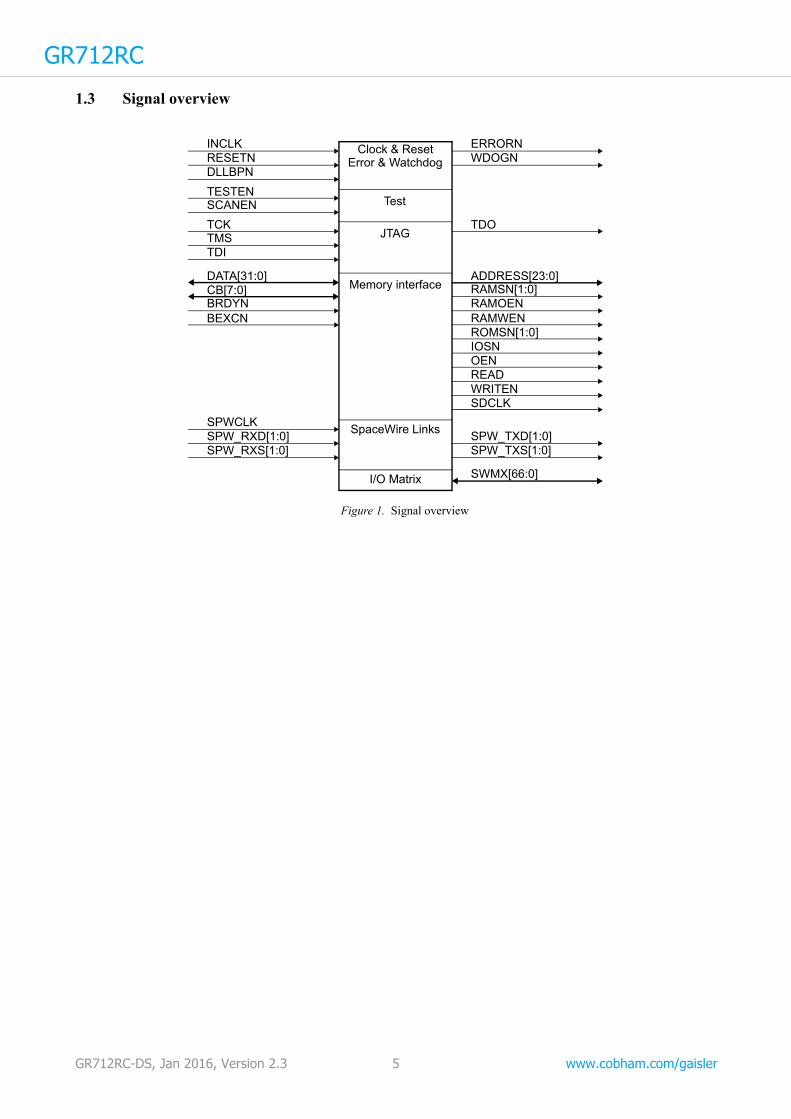
1.3 Signal overviewFigure 1. Signal overview
DLLBPN
ADDRESS[23:0]DATA[31:0]CB[7:0] RAMSN[1:0]
RAMOENRAMWENROMSN[1:0]IOSNOENREADWRITEN
BRDYNBEXCN
INCLKRESETN
ERRORNWDOGN
SPWCLKSPW_RXD[1:0]SPW_RXS[1:0]
SPW_TXD[1:0]SPW_TXS[1:0]
Memory interface
SpaceWire Links
Clock & ResetError & Watchdog
TCKTMSTDI
TDOJTAG
SDCLK
SWMX[66:0]I/O Matrix
TESTENSCANEN Test
GR712RC-DS, Jan 2016, Version 2.3 5 www.cobham.com/gaisler
GR712RC
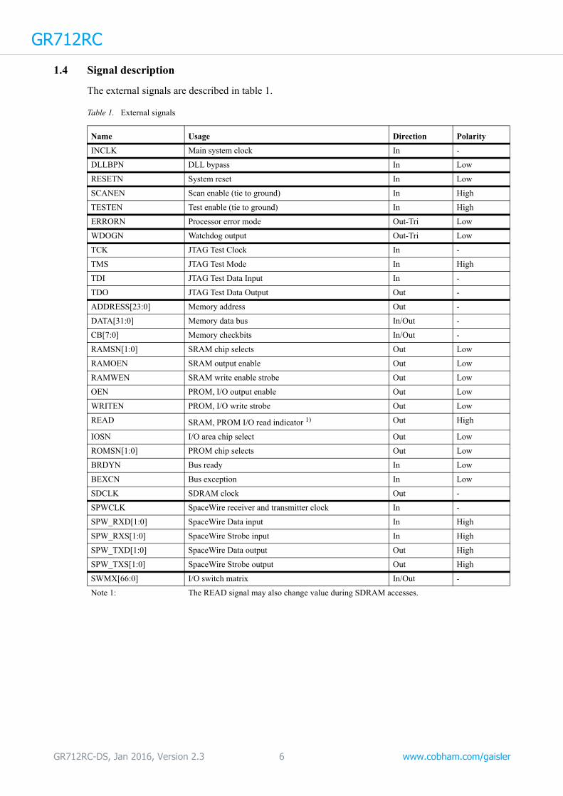
1.4 Signal descriptionThe external signals are described in table 1.
Table 1. External signals
Name Usage Direction Polarity
INCLK Main system clock In -
DLLBPN DLL bypass In Low
RESETN System reset In Low
SCANEN Scan enable (tie to ground) In High
TESTEN Test enable (tie to ground) In High
ERRORN Processor error mode Out-Tri Low
WDOGN Watchdog output Out-Tri Low
TCK JTAG Test Clock In -
TMS JTAG Test Mode In High
TDI JTAG Test Data Input In -
TDO JTAG Test Data Output Out -
ADDRESS[23:0] Memory address Out -
DATA[31:0] Memory data bus In/Out -
CB[7:0] Memory checkbits In/Out -
RAMSN[1:0] SRAM chip selects Out Low
RAMOEN SRAM output enable Out Low
RAMWEN SRAM write enable strobe Out Low
OEN PROM, I/O output enable Out Low
WRITEN PROM, I/O write strobe Out Low
READ SRAM, PROM I/O read indicator 1) Out High
IOSN I/O area chip select Out Low
ROMSN[1:0] PROM chip selects Out Low
BRDYN Bus ready In Low
BEXCN Bus exception In Low
SDCLK SDRAM clock Out -
SPWCLK SpaceWire receiver and transmitter clock In -
SPW_RXD[1:0] SpaceWire Data input In High
SPW_RXS[1:0] SpaceWire Strobe input In High
SPW_TXD[1:0] SpaceWire Data output Out High
SPW_TXS[1:0] SpaceWire Strobe output Out High
SWMX[66:0] I/O switch matrix In/Out -
Note 1: The READ signal may also change value during SDRAM accesses.
GR712RC-DS, Jan 2016, Version 2.3 6 www.cobham.com/gaisler
GR712RC
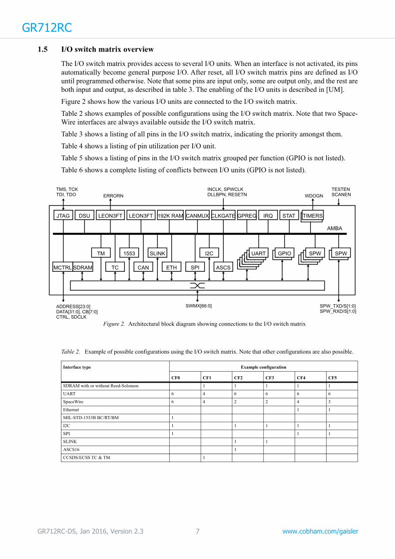
1.5 I/O switch matrix overviewThe I/O switch matrix provides access to several I/O units. When an interface is not activated, its pins automatically become general purpose I/O. After reset, all I/O switch matrix pins are defined as I/O until programmed otherwise. Note that some pins are input only, some are output only, and the rest are both input and output, as described in table 3. The enabling of the I/O units is described in [UM].
Figure 2 shows how the various I/O units are connected to the I/O switch matrix.
Table 2 shows examples of possible configurations using the I/O switch matrix. Note that two Space-Wire interfaces are always available outside the I/O switch matrix.
Table 3 shows a listing of all pins in the I/O switch matrix, indicating the priority amongst them.
Table 4 shows a listing of pin utilization per I/O unit.
Table 5 shows a listing of pins in the I/O switch matrix grouped per function (GPIO is not listed).
Table 6 shows a complete listing of conflicts between I/O units (GPIO is not listed).
Table 2. Example of possible configurations using the I/O switch matrix. Note that other configurations are also possible.
Interface type Example configuration
CF0 CF1 CF2 CF3 CF4 CF5
SDRAM with or without Reed-Solomon 1 1 1 1 1
UART 6 4 6 6 6 6
SpaceWire 6 4 2 2 4 3
Ethernet 1 1
MIL-STD-1553B BC/RT/BM 1
I2C 1 1 1 1 1
SPI 1 1 1
SLINK 1 1
ASCS16 1
CCSDS/ECSS TC & TM 1
Figure 2. Architectural block diagram showing connections to the I/O switch matrix
CAN
TM I2C
SPI ASCS
GPIOGPIO
TIMERSIRQ
SDRAM TCMCTRL
1553
ETH
SLINK
JTAG DSU
SPWSPWSPWSPWSPWSPW
STAT
UARTUARTUARTUARTUARTUART
192K RAM CANMUX GPREGCLKGATELEON3FT LEON3FT
AMBA
ERRORN WDOGN
TMS, TCK INCLK, SPWCLK
ADDRESS[23:0] SWMX[66:0] SPW_TXD/S[1:0]SPW_RXD/S[1:0]DATA[31:0], CB[7:0]
CTRL, SDCLK
DLLBPN, RESETNTESTENSCANENTDI, TDO
GR712RC-DS, Jan 2016, Version 2.3 7 www.cobham.com/gaisler
GR712RC
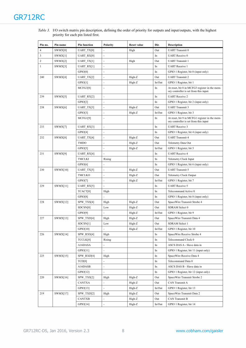
Table 3. I/O switch matrix pin description, defining the order of priority for outputs and input/outputs, with the highestpriority for each pin listed first.
Pin no. Pin name Pin function Polarity Reset value Dir. Description
4 SWMX[0] UART_TX[0] - High Out UART Transmit 0
3 SWMX[1] UART_RX[0] - In UART Receive 0
2 SWMX[2] UART_TX[1] - High Out UART Transmit 1
1 SWMX[3] UART_RX[1] - In UART Receive 1
GPIO[0] - In GPIO 1 Register, bit 0 (input only)
240 SWMX[4] UART_TX[2] - High-Z Out UART Transmit 2
GPIO[1] - High-Z In/Out GPIO 1 Register, bit 1
MCFG3[8] - In At reset, bit 8 in MCFG3 register in the mem-ory controller is set from this input.
239 SWMX[5] UART_RX[2] - In UART Receive 2
GPIO[2] - In GPIO 1 Register, bit 2 (input only)
238 SWMX[6] UART_TX[3] - High-Z Out UART Transmit 3
GPIO[3] - High-Z In/Out GPIO 1 Register, bit 3
MCFG1[9] - In At reset, bit 9 in MCFG1 register in the mem-ory controller is set from this input
233 SWMX[7] UART_RX[3] - In UART Receive 3
GPIO[4] - In GPIO 1 Register, bit 4 (input only)
232 SWMX[8] UART_TX[4] - High-Z Out UART Transmit 4
TMDO - High-Z Out Telemetry Data Out
GPIO[5] - High-Z In/Out GPIO 1 Register, bit 5
231 SWMX[9] UART_RX[4] - In UART Receive 4
TMCLKI Rising In Telemetry Clock Input
GPIO[6] - In GPIO 1 Register, bit 6 (input only)
230 SWMX[10] UART_TX[5] - High-Z Out UART Transmit 5
TMCLKO - High-Z Out Telemetry Clock Output
GPIO[7] - High-Z In/Out GPIO 1 Register, bit 7
229 SWMX[11] UART_RX[5] - In UART Receive 5
TCACT[0] High In Telecommand Active 0
GPIO[8] - In GPIO 1 Register, bit 8 (input only)
228 SWMX[12] SPW_TXS[4] High High-Z Out SpaceWire Transmit Strobe 4
SDCSN[0] Low High-Z Out SDRAM Select 0
GPIO[9] - High-Z In/Out GPIO 1 Register, bit 9
227 SWMX[13] SPW_TXD[4] High High-Z Out SpaceWire Transmit Data 4
SDCSN[1] Low High-Z Out SDRAM Select 1
GPIO[10] - High-Z In/Out GPIO 1 Register, bit 10
226 SWMX[14] SPW_RXS[4] High In SpaceWire Receive Strobe 4
TCCLK[0] Rising In Telecommand Clock 0
A16DASA - In ASCS DAS A - Slave data in
GPIO[11] - In GPIO 1 Register, bit 11 (input only)
225 SWMX[15] SPW_RXD[4] High In SpaceWire Receive Data 4
TCD[0] - In Telecommand Data 0
A16DASB - In ASCS DAS B - Slave data in
GPIO[12] - In GPIO 1 Register, bit 12 (input only)
220 SWMX[16] SPW_TXS[2] High High-Z Out SpaceWire Transmit Strobe 2
CANTXA - High-Z Out CAN Transmit A
GPIO[13] - High-Z In/Out GPIO 1 Register, bit 13
219 SWMX[17] SPW_TXD[2] High High-Z Out SpaceWire Transmit Data 2
CANTXB - High-Z Out CAN Transmit B
GPIO[14] - High-Z In/Out GPIO 1 Register, bit 14
GR712RC-DS, Jan 2016, Version 2.3 8 www.cobham.com/gaisler

GR712RC
218 SWMX[18] SPW_RXS[2] High In SpaceWire Receive Strobe 2
CANRXA - In CAN Receive A
GPIO[15] - In GPIO 1 Register, bit 15 (input only)
217 SWMX[19] SPW_RXD[2] High In SpaceWire Receive Data 2
CANRXB - In CAN Receive B
GPIO[16] - In GPIO 1 Register, bit 16 (input only)
203 SWMX[20] SPW_TXS[3] High High-Z Out SpaceWire Transmit Strobe 3
SLSYNC High High-Z Out SLINK SYNC
GPIO[17] - High-Z In/Out GPIO 1 Register, bit 17
202 SWMX[21] SPW_TXD[3] High High-Z Out SpaceWire Transmit Data 3
A16ETR High High-Z Out ASCS ETR - Synchronization signal
GPIO[18] - High-Z In/Out GPIO 1 Register, bit 18
201 SWMX[22] SPW_RXS[3]] High In SpaceWire Receive Strobe 3
GPIO[19] - In GPIO 1 Register, bit 19 (input only)
200 SWMX[23] SPW_RXD[3] High In SpaceWire Receive Data 3
GPIO[20] - In GPIO 1 Register, bit 20 (input only)
197 SWMX[24] SPW_TXD[5] High High-Z Out SpaceWire Transmit Data 5
SDDQM[0] High High-Z Out SDRAM Data Mask 0, corresponds to DATA[7:0]
GPIO[21] - High-Z In/Out GPIO 1 Register, bit 21
196 SWMX[25] SPW_TXS[5] High High-Z Out SpaceWire Transmit Strobe 5
SDDQM[1] High High-Z Out SDRAM Data Mask 1, corresponds to DATA[15:8]
GPIO[22] - High-Z In/Out GPIO 1 Register, bit 22
193 SWMX[26] SPW_RXS[5] High In SpaceWire Receive Strobe 5
TCRFAVL[0] High In Telecommand RF Available 0
GPIO[23] - In GPIO 1 Register, bit 23 (input only)
192 SWMX[27] SPW_RXD[5] High In SpaceWire Receive Data 5
TCCLK[1] Rising In Telecommand Clock 1
GPIO[24] - In GPIO 1 Register, bit 24 (input only)
191 SWMX[28] 1553RXENA High High-Z Out MIL-STD-1553B Receive Enable A
- High-Z Out Proprietary, enabled by CAN
RMTXD[0] - High-Z Out Ethernet Transmit Data 0
GPIO[25] - High-Z In/Out GPIO 1 Register, bit 25
190 SWMX[29] 1553TXA High High-Z Out MIL-STD-1553B Transmit Positive A
- High-Z Out Proprietary, enabled by CAN
RMTXD[1] - High-Z Out Ethernet Transmit Data 1
GPIO[26] - High-Z In/Out GPIO 1 Register, bit 26
189 SWMX[30] 1553RXA High In MIL-STD-1553B Receive Positive A
TCD[1] - In Telecommand Data 1
RMRXD[0] - In Ethernet Receive Data 0
GPIO[27] - In GPIO 1 Register, bit 27 (input only)
188 SWMX[31] 1553RXNA Low In MIL-STD-1553B Receive Negative A
TCACT[1] High In Telecommand Active 1
RMRXD[1] - In Ethernet Receive Data 1
GPIO[28] - In GPIO 1 Register, bit 28 (input only)
185 SWMX[32] 1553TXNA Low High-Z Out MIL-STD-1553B Transmit Negative A
- High-Z Out Proprietary, enabled by CAN
RMTXEN High High-Z Out Ethernet Transmit Enable
GPIO[29] - High-Z In/Out GPIO 1 Register, bit 29
184 SWMX[33] 1553TXINHA High High-Z Out MIL-STD-1553B Transmit Inhibit A
Table 3. I/O switch matrix pin description, defining the order of priority for outputs and input/outputs, with the highest priority for each pin listed first.
Pin no. Pin name Pin function Polarity Reset value Dir. Description
GR712RC-DS, Jan 2016, Version 2.3 9 www.cobham.com/gaisler

GR712RC
- High-Z Out Proprietary, enabled by CAN
GPIO[30] - High-Z In/Out GPIO 1 Register, bit 30
183 SWMX[34] 1553RXB High In MIL-STD-1553B Receive Positive B
TCRFAVL[1] High In Telecommand RF Available 1
RMCRSDV High In Ethernet Carrier Sense / Data Valid
GPIO[31] - In GPIO 1 Register, bit 31 (input only)
182 SWMX[35] 1553RXNB Low In MIL-STD-1553B Receive Negative B
TCCLK[2] Rising In Telecommand Clock 2
RMINTN Low In Ethernet Management Interrupt
GPIO[32] - In GPIO 2 Register, bit 0 (input only)
179 SWMX[36] 1553RXENB High High-Z Out MIL-STD-1553B Receive Enable B
A16MCS High High-Z Out ASCS MCS - TM start/stop signal
RMMDIO - High-Z In/Out Ethernet Media Interface Data
GPIO[33] - High-Z In/Out GPIO 2 Register, bit 1
178 SWMX[37] 1553TXB High High-Z Out MIL-STD-1553B Transmit Positive B
A16HS High High-Z Out ASCS HS - TM/TC serial clock
RMMDC - High-Z Out Ethernet Media Interface Clock
GPIO[34] - High-Z In/Out GPIO 2 Register, bit 2
SpaceWire clock divisor registers
- In At reset, bits 8 and 0 in the clock divisor reg-ister of the SpaceWire interfaces are set from this input
177 SWMX[38] 1553CK - In MIL-STD-1553B Clock
TCD[2] - In Telecommand Data 2
RMRFCLK - In Ethernet Reference Clock
GPIO[35] - In GPIO 2 Register, bit 3 (input only)
176 SWMX[39] TCACT[2] High In Telecommand Active 2
GPIO[36] - In GPIO 2 Register, bit 4 (input only)
175 SWMX[40] 1553TXNB Low High-Z Out MIL-STD-1553B Transmit Negative B
A16DCS - High-Z Out ASCS DCS - Slave data out
GPIO[37] - High-Z In/Out GPIO 2 Register, bit 5
SpaceWire clock divisor registers
- In At reset, bits 9 and 1 in the clock divisor reg-ister of the SpaceWire interfaces are set from this input
174 SWMX[41] 1553TXINHB High High-Z Out MIL-STD-1553B Transmit Inhibit B
A16MAS High High-Z Out ASCS MAS - TM start/stop signal
GPIO[38] - High-Z In/Out GPIO 2 Register, bit 6
173 SWMX[42] TCRFAVL[2] High In Telecommand RF Available 2
GPIO[39] - In GPIO 2 Register, bit 7 (input only)
172 SWMX[43] - High-Z Out Proprietary, enabled by CAN
GPIO[40] - High-Z In/Out GPIO 2 Register, bit 8
SpaceWire clock divisor registers
- In At reset, bits 10 and 2 in the clock divisor reg-ister of the SpaceWire interfaces are set from this input
169 SWMX[44] SPICLK High-Z Out SPI Clock
SLO - High-Z Out SLINK Data Out
GPIO[41] - High-Z In/Out GPIO 2 Register, bit 9
166 SWMX[45] SPIMOSI - High-Z Out SPI Master Out Slave In
SLCLK High High-Z Out SLINK Clock
GPIO[42] - High-Z In/Out GPIO 2 Register, bit 10
SpaceWire clock divisor registers
- In At reset, bits 11 and 3 in the clock divisor reg-ister of the SpaceWire interfaces are set from this input
165 SWMX[46] TCCLK[3] Rising In Telecommand Clock 3
GPIO[43] - In GPIO 2 Register, bit 11 (input only)
Table 3. I/O switch matrix pin description, defining the order of priority for outputs and input/outputs, with the highest priority for each pin listed first.
Pin no. Pin name Pin function Polarity Reset value Dir. Description
GR712RC-DS, Jan 2016, Version 2.3 10 www.cobham.com/gaisler
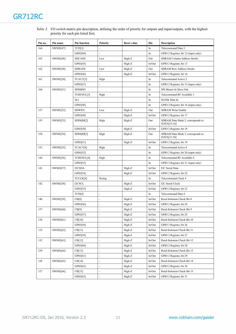
GR712RC
164 SWMX[47] TCD[3] - In Telecommand Data 3
GPIO[44] - In GPIO 2 Register, bit 12 (input only)
163 SWMX[48] SDCASN Low High-Z Out SDRAM Column Address Strobe
GPIO[45] - High-Z In/Out GPIO 2 Register, bit 13
162 SWMX[49] SDRASN Low High-Z Out SDRAM Row Address Strobe
GPIO[46] - High-Z In/Out GPIO 2 Register, bit 14
161 SWMX[50] TCACT[3] High In Telecommand Active 3
GPIO[47] - In GPIO 2 Register, bit 15 (input only)
160 SWMX[51] SPIMISO In SPI Master In Slave Out
TCRFAVL[3] High In Telecommand RF Available 3
SLI - In SLINK Data In
GPIO[48] - In GPIO 2 Register, bit 16 (input only)
157 SWMX[52] SDWEN Low High-Z Out SDRAM Write Enable
GPIO[49] - High-Z In/Out GPIO 2 Register, bit 17
155 SWMX[53] SDDQM[2] High High-Z Out SDRAM Data Mask 2, corresponds to DATA[23:16]
GPIO[50] - High-Z In/Out GPIO 2 Register, bit 18
154 SWMX[54] SDDQM[3] High High-Z Out SDRAM Data Mask 3, corresponds to DATA[31:24]
GPIO[51] - High-Z In/Out GPIO 2 Register, bit 19
153 SWMX[55] TCACT[4] High In Telecommand Active 4
GPIO[52] - In GPIO 2 Register, bit 20 (input only)
144 SWMX[56] TCRFAVL[4] High In Telecommand RF Available 4
GPIO[53] - In GPIO 2 Register, bit 21 (input only)
143 SWMX[57] I2CSDA High-Z In/Out I2C Serial Data
GPIO[54] - High-Z In/Out GPIO 2 Register, bit 22
TCCLK[4] Rising In Telecommand Clock 4
142 SWMX[58] I2CSCL High-Z In/Out I2C Serial Clock
GPIO[55] - High-Z In/Out GPIO 2 Register, bit 23
TCD[4] - In Telecommand Data 4
140 SWMX[59] CB[8] - High-Z In/Out Reed-Solomon Check Bit 8
GPIO[56] - High-Z In/Out GPIO 2 Register, bit 24
137 SWMX[60] CB[9] - High-Z In/Out Reed-Solomon Check Bit 9
GPIO[57] - High-Z In/Out GPIO 2 Register, bit 25
136 SWMX[61] CB[10] - High-Z In/Out Reed-Solomon Check Bit 10
GPIO[58] - High-Z In/Out GPIO 2 Register, bit 26
135 SWMX[62] CB[11] - High-Z In/Out Reed-Solomon Check Bit 11
GPIO[59] - High-Z In/Out GPIO 2 Register, bit 27
132 SWMX[63] CB[12] - High-Z In/Out Reed-Solomon Check Bit 12
GPIO[60] - High-Z In/Out GPIO 2 Register, bit 28
129 SWMX[64] CB[13] - High-Z In/Out Reed-Solomon Check Bit 13
GPIO[61] - High-Z In/Out GPIO 2 Register, bit 29
128 SWMX[65] CB[14] - High-Z In/Out Reed-Solomon Check Bit 14
GPIO[62] - High-Z In/Out GPIO 2 Register, bit 30
127 SWMX[66] CB[15] - High-Z In/Out Reed-Solomon Check Bit 15
GPIO[63] - High-Z In/Out GPIO 2 Register, bit 31
Table 3. I/O switch matrix pin description, defining the order of priority for outputs and input/outputs, with the highest priority for each pin listed first.
Pin no. Pin name Pin function Polarity Reset value Dir. Description
GR712RC-DS, Jan 2016, Version 2.3 11 www.cobham.com/gaisler

GR712RC
Table 4. I/O switch matrix pin utilization per interface typeInterface type Pin function Direction Total
In Out In/Out
SDRAM SDDQM[3:0], SDCASN, SDRASN, SDWEN, SDCSN[1:0] 9 9
SDRAM Reed-Solomon CB[15:8] 8 8
GPIO GPIO[...] 26 38 64
UART UART_TX[5:0], UART_RX[5:0] 6 6 12
SpaceWire SPW_RXD[5:2], SPW_RXS[5:2], SPW_TXD[5:2], SPW_TXS[5:2] 8 8 16
Ethernet RMTXD[1:0], RMTXEN, RMMDIO, RMMDC 5 4 1 10
RMRFCLK, RMRXD[0:1], RMCRSDV, RMINTN
CAN CANTXA, CANRXA, CANTXB, CANRXB 4 4 8
MIL-STD-1553B BC/RT/BM 1553RXA, 1553RXNA, 1553RXENA, 1553TXA, 1553TXNA, 1553TXINHA 5 8 13
1553RXB, 1553RXNB, 1553RXENB, 1553TXB, 1553TXNB, 1553TXINHB
1553CK
I2C I2CSDA, I2CSCL 2 2
SPI SPICLK, SPIMOSI, SPIMISO 1 2 3
SLINK SLI, SLO, SLSYNC, SLCLK 1 3 4
ASCS16 A16DASA, A16DASB, A16MCS, A16HS, A16DCS, A16MAS, A16ETR 2 5 7
CCSDS/ECSS TC TCACT[4:0], TCD[4:0], TCCLK[4:0], TCRFAV[4:0] 20 20
CCSDS/ECSS TM TMDO, TMCLKO, TMCLKI 1 2 3
GR712RC-DS, Jan 2016, Version 2.3 12 www.cobham.com/gaisler

GR712RC
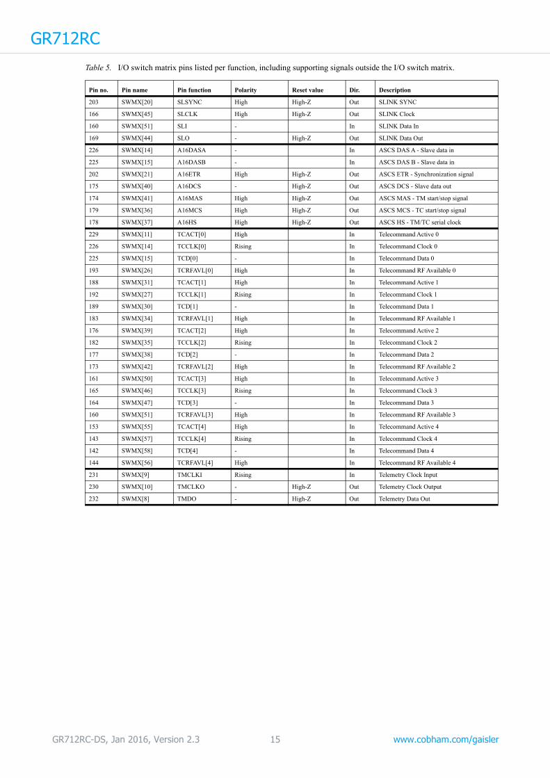
Table 5. I/O switch matrix pins listed per function, including supporting signals outside the I/O switch matrix.Pin no. Pin name Pin function Polarity Reset value Dir. Description
157 SWMX[52] SDWEN Low High-Z Out SDRAM Write Enable
163 SWMX[48] SDCASN Low High-Z Out SDRAM Column Address Strobe
162 SWMX[49] SDRASN Low High-Z Out SDRAM Row Address Strobe
228 SWMX[12] SDCSN[0] Low High-Z Out SDRAM Select 0
227 SWMX[13] SDCSN[1] Low High-Z Out SDRAM Select 1
197 SWMX[24] SDDQM[0] High High-Z Out SDRAM Data Mask 0, corresponds to DATA[7:0]
196 SWMX[25] SDDQM[1] High High-Z Out SDRAM Data Mask 1, corresponds to DATA[15:8]
155 SWMX[53] SDDQM[2] High High-Z Out SDRAM Data Mask 2, corresponds to DATA[23:16]
154 SWMX[54] SDDQM[3] High High-Z Out SDRAM Data Mask 3, corresponds to DATA[31:24]
140 SWMX[59] CB[8] - High-Z In/Out Check Bit 8, Reed-Solomon
137 SWMX[60] CB[9] - High-Z In/Out Check Bit 9, Reed-Solomon
136 SWMX[61] CB[10] - High-Z In/Out Check Bit 10, Reed-Solomon
135 SWMX[62] CB[11] - High-Z In/Out Check Bit 11, Reed-Solomon
132 SWMX[63] CB[12] - High-Z In/Out Check Bit 12, Reed-Solomon
129 SWMX[64] CB[13] - High-Z In/Out Check Bit 13, Reed-Solomon
128 SWMX[65] CB[14] - High-Z In/Out Check Bit 14, Reed-Solomon
127 SWMX[66] CB[15] - High-Z In/Out Check Bit 15, Reed-Solomon
ADDRESS[16:2] ADDRESS[16:2] - Low Out Memory address
DATA[31:0] DATA[31:0] - High-Z In/Out Memory data bus
CB[7:0] CB[7:0] - High-Z In/Out Memory checkbits
240 SWMX[4] MCFG3[8] - In At reset, bit 8 in MCFG3 register in the memory controller is set from this input.
238 SWMX[6] MCFG1[9] - In At reset, bit 9 in MCFG1 register in the memory controller is set from this input
4 SWMX[0] UART_TX[0] - High Out UART Transmit 0
3 SWMX[1] UART_RX[0] - In UART Receive 0
2 SWMX[2] UART_TX[1] - High Out UART Transmit 1
1 SWMX[3] UART_RX[1] - In UART Receive 1
240 SWMX[4] UART_TX[2] - High-Z Out UART Transmit 2
239 SWMX[5] UART_RX[2] - In UART Receive 2
238 SWMX[6] UART_TX[3] - High-Z Out UART Transmit 3
233 SWMX[7] UART_RX[3] - In UART Receive 3
232 SWMX[8] UART_TX[4] - High-Z Out UART Transmit 4
231 SWMX[9] UART_RX[4] - In UART Receive 4
230 SWMX[10] UART_TX[5] - High-Z Out UART Transmit 5
229 SWMX[11] UART_RX[5] - In UART Receive 5
213 SPW_RXD[0] SPW_RXD[0] High In SpaceWire Receive Data 0
214 SPW_RXS[0] SPW_RXS[0] High In SpaceWire Receive Strobe 0
215 SPW_TXD[0] SPW_TXD[0] High Low Out SpaceWire Transmit Data 0
216 SPW_TXS[0] SPW_TXS[0] High Low Out SpaceWire Transmit Strobe 0
204 SPW_RXD[1] SPW_RXD[1] High In SpaceWire Receive Data 1
205 SPW_RXS[1] SPW_RXS[1] High In SpaceWire Receive Strobe 1
206 SPW_TXD[1] SPW_TXD[1] High Low Out SpaceWire Transmit Data 1
209 SPW_TXS[1] SPW_TXS[1] High Low Out SpaceWire Transmit Strobe 1
217 SWMX[19] SPW_RXD[2] High In SpaceWire Receive Data 2
218 SWMX[18] SPW_RXS[2] High In SpaceWire Receive Strobe 2
219 SWMX[17] SPW_TXD[2] High High-Z Out SpaceWire Transmit Data 2
220 SWMX[16] SPW_TXS[2] High High-Z Out SpaceWire Transmit Strobe 2
200 SWMX[23] SPW_RXD[3] High In SpaceWire Receive Data 3
201 SWMX[22] SPW_RXS[3] High In SpaceWire Receive Strobe 3
GR712RC-DS, Jan 2016, Version 2.3 13 www.cobham.com/gaisler

GR712RC
202 SWMX[21] SPW_TXD[3] High High-Z Out SpaceWire Transmit Data 3
203 SWMX[20] SPW_TXS[3] High High-Z Out SpaceWire Transmit Strobe 3
225 SWMX[15] SPW_RXD[4] High In SpaceWire Receive Data 4
226 SWMX[14] SPW_RXS[4] High In SpaceWire Receive Strobe 4
227 SWMX[13] SPW_TXD[4] High High-Z Out SpaceWire Transmit Data 4
228 SWMX[12] SPW_TXS[4] High High-Z Out SpaceWire Transmit Strobe 4
192 SWMX[27] SPW_RXD[5] High In SpaceWire Receive Data 5
193 SWMX[26] SPW_RXS[5] High In SpaceWire Receive Strobe 5
197 SWMX[24] SPW_TXD[5] High High-Z Out SpaceWire Transmit Data 5
196 SWMX[25] SPW_TXS[5] High High-Z Out SpaceWire Transmit Strobe 5
178 SWMX[37] SpaceWire clock divisor registers values at reset, all other bits are zero.
- In At reset, bits 8 & 0 are set from this input
175 SWMX[40] - In At reset, bits 9 & 1 are set from this input
172 SWMX[43] - In At reset, bits 10 & 2 are set from this input
166 SWMX[45] - In At reset, bits 11 & 3 are set from this input
185 SWMX[32] RMTXEN High High-Z Out Ethernet Transmit Enable
191 SWMX[28] RMTXD[0] - High-Z Out Ethernet Transmit Data 0
190 SWMX[29] RMTXD[1] - High-Z Out Ethernet Transmit Data 1
189 SWMX[30] RMRXD[0] - In Ethernet Receive Data 0
188 SWMX[31] RMRXD[1] - In Ethernet Receive Data 1
183 SWMX[34] RMCRSDV High In Ethernet Carrier Sense / Data Valid
182 SWMX[35] RMINTN Low In Ethernet Management Interrupt
179 SWMX[36] RMMDIO - High-Z In/Out Ethernet Media Interface Data
178 SWMX[37] RMMDC - High-Z Out Ethernet Media Interface Clock
177 SWMX[38] RMRFCLK - In Ethernet Reference Clock
220 SWMX[16] CANTXA - High-Z Out CAN Transmit A
218 SWMX[18] CANRXA - In CAN Receive A
219 SWMX[17] CANTXB - High-Z Out CAN Transmit B
217 SWMX[19] CANRXB - In CAN Receive B
191 SWMX[28] - High-Z Out Proprietary, enabled by CAN
190 SWMX[29] - High-Z Out Proprietary, enabled by CAN
185 SWMX[32] - High-Z Out Proprietary, enabled by CAN
184 SWMX[33] - High-Z Out Proprietary, enabled by CAN
172 SWMX[43] - High-Z Out Proprietary, enabled by CAN
177 SWMX[38] 1553CK - In MIL-STD-1553B Clock
184 SWMX[33] 1553TXINHA High High-Z Out MIL-STD-1553B Transmit Inhibit A
190 SWMX[29] 1553TXA High High-Z Out MIL-STD-1553B Transmit Positive A
185 SWMX[32] 1553TXNA Low High-Z Out MIL-STD-1553B Transmit Negative A
191 SWMX[28] 1553RXENA High High-Z Out MIL-STD-1553B Receive Enable A
189 SWMX[30] 1553RXA High In MIL-STD-1553B Receive Positive A
188 SWMX[31] 1553RXNA Low In MIL-STD-1553B Receive Negative A
174 SWMX[41] 1553TXINHB High High-Z Out MIL-STD-1553B Transmit Inhibit B
178 SWMX[37] 1553TXB High High-Z Out MIL-STD-1553B Transmit Positive B
175 SWMX[40] 1553TXNB Low High-Z Out MIL-STD-1553B Transmit Negative B
179 SWMX[36] 1553RXENB High High-Z Out MIL-STD-1553B Receive Enable B
183 SWMX[34] 1553RXB High In MIL-STD-1553B Receive Positive B
182 SWMX[35] 1553RXNB Low In MIL-STD-1553B Receive Negative B
143 SWMX[57] I2CSDA High-Z In/Out I2C Serial Data
142 SWMX[58] I2CSCL High-Z In/Out I2C Serial Clock
169 SWMX[44] SPICLK High-Z Out SPI Clock
166 SWMX[45] SPIMOSI - High-Z Out SPI Master Out Slave In
160 SWMX[51] SPIMISO In SPI Master In Slave Out
Table 5. I/O switch matrix pins listed per function, including supporting signals outside the I/O switch matrix.
Pin no. Pin name Pin function Polarity Reset value Dir. Description
GR712RC-DS, Jan 2016, Version 2.3 14 www.cobham.com/gaisler
GR712RC
203 SWMX[20] SLSYNC High High-Z Out SLINK SYNC
166 SWMX[45] SLCLK High High-Z Out SLINK Clock
160 SWMX[51] SLI - In SLINK Data In
169 SWMX[44] SLO - High-Z Out SLINK Data Out
226 SWMX[14] A16DASA - In ASCS DAS A - Slave data in
225 SWMX[15] A16DASB - In ASCS DAS B - Slave data in
202 SWMX[21] A16ETR High High-Z Out ASCS ETR - Synchronization signal
175 SWMX[40] A16DCS - High-Z Out ASCS DCS - Slave data out
174 SWMX[41] A16MAS High High-Z Out ASCS MAS - TM start/stop signal
179 SWMX[36] A16MCS High High-Z Out ASCS MCS - TC start/stop signal
178 SWMX[37] A16HS High High-Z Out ASCS HS - TM/TC serial clock
229 SWMX[11] TCACT[0] High In Telecommand Active 0
226 SWMX[14] TCCLK[0] Rising In Telecommand Clock 0
225 SWMX[15] TCD[0] - In Telecommand Data 0
193 SWMX[26] TCRFAVL[0] High In Telecommand RF Available 0
188 SWMX[31] TCACT[1] High In Telecommand Active 1
192 SWMX[27] TCCLK[1] Rising In Telecommand Clock 1
189 SWMX[30] TCD[1] - In Telecommand Data 1
183 SWMX[34] TCRFAVL[1] High In Telecommand RF Available 1
176 SWMX[39] TCACT[2] High In Telecommand Active 2
182 SWMX[35] TCCLK[2] Rising In Telecommand Clock 2
177 SWMX[38] TCD[2] - In Telecommand Data 2
173 SWMX[42] TCRFAVL[2] High In Telecommand RF Available 2
161 SWMX[50] TCACT[3] High In Telecommand Active 3
165 SWMX[46] TCCLK[3] Rising In Telecommand Clock 3
164 SWMX[47] TCD[3] - In Telecommand Data 3
160 SWMX[51] TCRFAVL[3] High In Telecommand RF Available 3
153 SWMX[55] TCACT[4] High In Telecommand Active 4
143 SWMX[57] TCCLK[4] Rising In Telecommand Clock 4
142 SWMX[58] TCD[4] - In Telecommand Data 4
144 SWMX[56] TCRFAVL[4] High In Telecommand RF Available 4
231 SWMX[9] TMCLKI Rising In Telemetry Clock Input
230 SWMX[10] TMCLKO - High-Z Out Telemetry Clock Output
232 SWMX[8] TMDO - High-Z Out Telemetry Data Out
Table 5. I/O switch matrix pins listed per function, including supporting signals outside the I/O switch matrix.
Pin no. Pin name Pin function Polarity Reset value Dir. Description
GR712RC-DS, Jan 2016, Version 2.3 15 www.cobham.com/gaisler

GR712RC
Table 6. Conflicting interfaces in the I/O switch matrix are marked with an X, with duplicates shown in bold typeface.SDRAM (with RS) - X X
UART 0 -
UART 1 -
UART 2 -
UART 3 -
UART 4 - X
UART 5 - X X
SpaceWire 0 -
SpaceWire 1 -
SpaceWire 2 - X X
SpaceWire 3 - X
SpaceWire 4 X - X X
SpaceWire 5 X - X X
Ethernet - X X X X
CAN X X -
MIL-STD-1553B X - X X X
I2C - X
SPI - X X
SLINK X X - X
ASCS X X X - X
CCSDS TC 0 X X X X -
CCSDS TC 1 X X X -
CCSDS TC 2 X X -
CCSDS TC 3 X X -
CCSDS TC 4 X -
CCSDS TM X X -
SD
RA
M (
wit
h R
S)
UA
RT
0
UA
RT
1
UA
RT
2
UA
RT
3
UA
RT
4
UA
RT
5
Spa
ceW
ire
0
Spa
ceW
ire
1
Spa
ceW
ire
2
Spa
ceW
ire
3
Spa
ceW
ire
4
Spa
ceW
ire
5
Eth
erne
t
CA
N
MIL
-ST
D-1
553B
I2C
SPI
SL
INK
AS
CS
CC
SD
S T
C 0
CC
SD
S T
C 1
CC
SD
S T
C 2
CC
SD
S T
C 3
CC
SD
S T
C 4
CC
SD
S T
M
GR712RC-DS, Jan 2016, Version 2.3 16 www.cobham.com/gaisler

GR712RC
2 Electrical characteristics2.1 Absolute maximum ratings
These values specify the stress that might apply to the device without causing it permanent damage.
2.2 Recommended operating conditions
Table 8. Recommended operating conditions
Table 7. Absolute maximum ratings 1)
Symbol Parameter Rating Units
Min. Max.
VDDIO DC Supply Voltage for I/O -0.3 4.2 V
VDD DC Supply Voltage for Core -0.3 2.4 V
VIN Input Voltage -0.3 VDDIO + 0.3 V
Tstor Storage Temperature -65 +150 °C
Tcase Operating Case Temperature -55 +125 °C
Tsolder Lead Temperature (Soldering 10 sec.) +250 °C
Tj Junction Temperature +150 °C
JC (ceramic) Thermal Resistance, Junction to Case 4 °C/W
PD Power Dissipation 6.25 W
Note 1: Extended operation at the maximum levels may degrade the performance and affect the reliability of the device.
Symbol Parameter Rating Units
Min. Typ. Max.
VDDIO DC Supply Voltage for I/O 3.0 3.3 3.6 V
VDD DC Supply Voltage for Core 1.65 1.8 1.95 V
VIN Input Voltage 0 VDDIO V
Tcase Operating Case Temperature -55 +125 °C
SLIN Slew rate of all inputs 1) 0.4 V/ns
Note 1: Applies only to the range 0.8V and 2.0V.
GR712RC-DS, Jan 2016, Version 2.3 17 www.cobham.com/gaisler

GR712RC
2.3 DC electrical performance characteristicsTable 9. DC characteristics (VDD = 1.8V +/- 0.15V, VDDIO = 3.3V +/- 0.3V, Tcase = -55°C to +125°C)
Symbol Parameter Condition Rating Units
Min. Typ. Max.
VOH Output High Voltage 1) IOH = -4 mA 2)
IOH = -6 mA 3)
2.4 V
VOL Output Low VoltageIOL = 4 mA 2)
IOL = 6 mA 3)
0.5 V
VIH Input High Voltage 2.0 V
VIL Input Low Voltage 0.8 V
IILEAK Input Leakage Current -30 7) 30 7) uA
IOLEAK Output Leakage Current outputs at tri-state
-30 7) 30 7) uA
IOS Short-circuit Output Current VO = VDDIO,
VDDIO = 3.6V120 5) mA
VO = 0V,
VDDIO = 3.6V-120 5)
IDDS Core Static Current FCLK = 0 MHz 1 250 8) mA
IDD Core Supply Current FCLK = 100 MHz 0.9 2.0 5) A
IDDIOS I/O Static Current 4) FCLK = 0 MHz
VDDIO = 3.6V
0.2 4 9) mA
IDDIO I/O Supply Current 6) mA
CI/O I/O Pad Capacitance 5) 15 pF
Note 1: Except open-drain outputs ERRORN, WDOGN, I2CSCL and I2CSDA.
Note 2: All outputs defined with a slow drive capability in the pin assignment table in section 3.2.
Note 3: All outputs defined with a fast drive capability in the pin assignment table in section 3.2.
Note 4: All inputs at 0 V or VDDIO. No resistive load.
Note 5: Supplied as a design limit. Parameter not measured during production test.
Note 6: The dynamic power consumption of the I/O supply can be calculated as a function of the average frequency and
the capacitive load of each output i: sum of [FI/O * CLOAD](i) * (VDDIO)2
Note 7: This parameter is degrading with TID radiation. Given value at 300 krad(Si). Leakage current up to 100 krad(Si) is +/-15 uA.
Note 8: This parameter is degrading with TID radiation. Given value at 300 krad(Si). Leakage current up to 100 krad(Si) is 10 mA.
Note 9: This parameter is degrading with TID radiation. Given value at 300 krad(Si). Leakage current up to 100 krad(Si) is 2 mA.
GR712RC-DS, Jan 2016, Version 2.3 18 www.cobham.com/gaisler
GR712RC
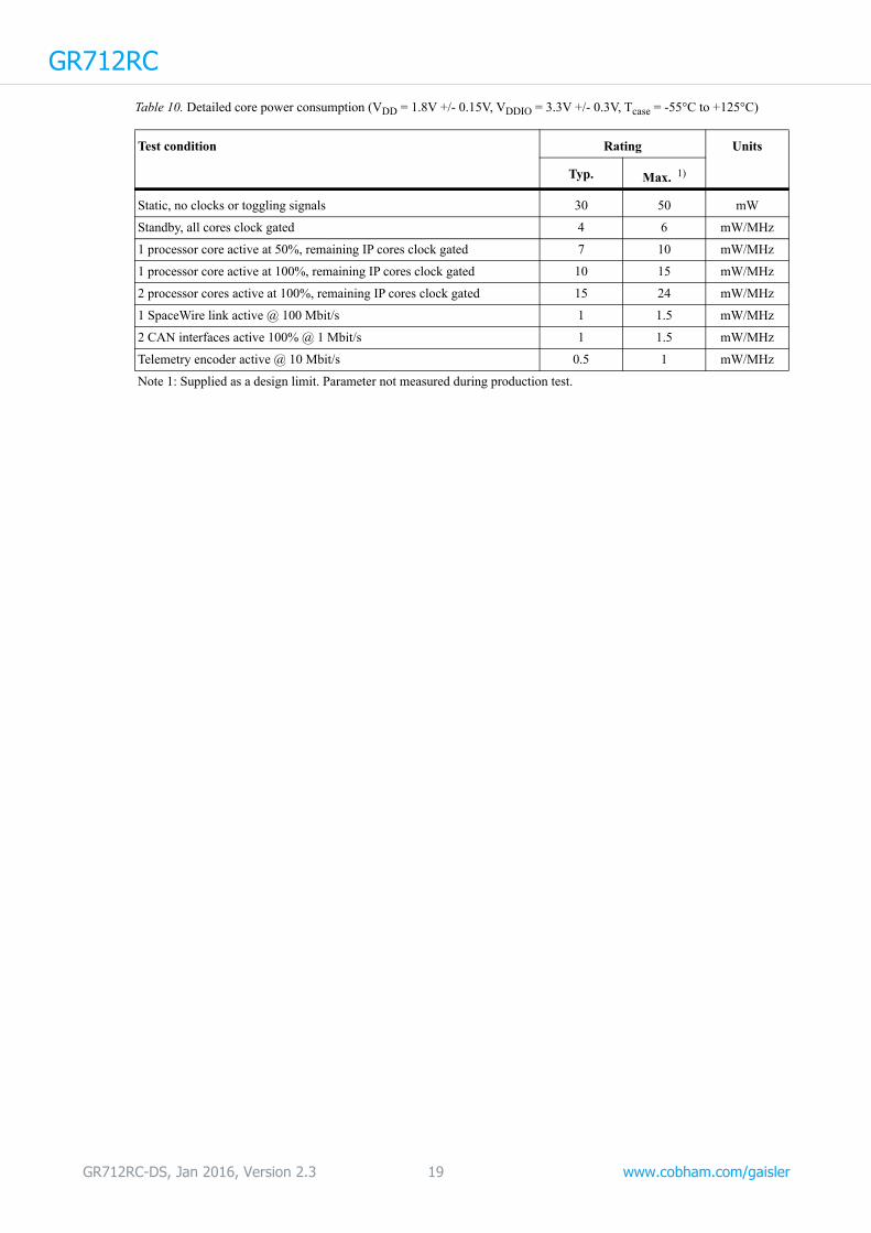
Table 10. Detailed core power consumption (VDD = 1.8V +/- 0.15V, VDDIO = 3.3V +/- 0.3V, Tcase = -55°C to +125°C)Test condition Rating Units
Typ. Max. 1)
Static, no clocks or toggling signals 30 50 mW
Standby, all cores clock gated 4 6 mW/MHz
1 processor core active at 50%, remaining IP cores clock gated 7 10 mW/MHz
1 processor core active at 100%, remaining IP cores clock gated 10 15 mW/MHz
2 processor cores active at 100%, remaining IP cores clock gated 15 24 mW/MHz
1 SpaceWire link active @ 100 Mbit/s 1 1.5 mW/MHz
2 CAN interfaces active 100% @ 1 Mbit/s 1 1.5 mW/MHz
Telemetry encoder active @ 10 Mbit/s 0.5 1 mW/MHz
Note 1: Supplied as a design limit. Parameter not measured during production test.
GR712RC-DS, Jan 2016, Version 2.3 19 www.cobham.com/gaisler

GR712RC
2.4 AC electrical performance characteristicsAll measured AC parameters have been tested with a 50 pF - 70 pF capacitive load on the outputs. Transition time measurements have been tested at a voltage level of 1.4 V. Equivalent load chart is provided in the product specification [PS.]
2.4.1 Clock
The timing waveforms and timing parameters are shown in figure 3 and are defined in table 11.
Table 11. Timing parameters (VDD = 1.8V +/- 0.15V, VDDIO = 3.3V +/- 0.3V, Tcase = -55°C to +125°C)
Name Parameter Reference Min Max Unit
TINCLK input clock period without DLL INCLK 10 - ns
FINCLK input clock frequency without DLL 2) INCLK - 100 MHz
TINCLK_HIGH input clock high phase without DLL 5) INCLK 4.5 ns
TINCLK_LOW input clock low phase without DLL 5) INCLK 4.5 ns
TINCLK input clock period with DLL 1) INCLK 20 22 3) ns
FINCLK input clock frequency with DLL 1) 2) INCLK 46 3) 50 MHz
DCINCLK input frequency duty cycle with DLL INCLK 35 65 %
TINCLK_HIGH input clock high phase with DLL 5) INCLK 7 ns
TINCLK_LOW input clock low phase with DLL 5) INCLK 7 ns
TCLK internal system clock period 4) 5) 6) - 10 - ns
FCLK internal system clock frequency 2) 4) 5) 6) - - 100 MHz
Note 1: For the system clock, the DLL provides a times 2 multiplication of the input frequency.
Note 2: TINCLK = 1/FINCLK, TCLK = 1/FCLK
Note 3: Parameter not measured during production test.
Note 4: Applies to the system clock only (i.e. processor and AMBA clock) only. SpaceWire clocks are dis-cussed in section 2.4.9.
Note 5: The maximum internal system clock frequency is specified by the parameters TCLK and FCLK.
The parameters TINCLK and FINCLK specify what the clock input pin and the DLL can support, and
not what the internal logic can support.
Note 6: The internal system clock frequency is limited by the timing of the memory interface towards external synchronous memory components.
Figure 3. Timing waveforms
INCLK
TINCLK
GR712RC-DS, Jan 2016, Version 2.3 20 www.cobham.com/gaisler
GR712RC
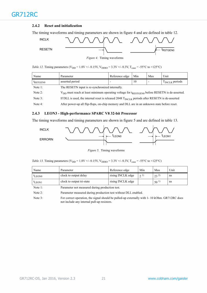
2.4.2 Reset and initializationThe timing waveforms and timing parameters are shown in figure 4 and are defined in table 12.
2.4.3 LEON3 - High-performance SPARC V8 32-bit Processor
The timing waveforms and timing parameters are shown in figure 5 and are defined in table 13.
Table 12. Timing parameters (VDD = 1.8V +/- 0.15V, VDDIO = 3.3V +/- 0.3V, Tcase = -55°C to +125°C)
Name Parameter Reference edge Min Max Unit
tRSTGEN0 asserted period - 10 - TINCLK periods
Note 1: The RESETN input is re-synchronized internally.
Note 2: VDD must reach at least minimum operating voltage for tRESTGEN0 before RESETN is de-asserted.
Note 3: If DLL is used, the internal reset is released 2048 TINCLK periods after RESETN is de-asserted
Note 4: After power-up all flip-flops, on-chip memory and DLL are in an unknown state before reset.
Table 13. Timing parameters (VDD = 1.8V +/- 0.15V, VDDIO = 3.3V +/- 0.3V, Tcase = -55°C to +125°C)
Name Parameter Reference edge Min Max Unit
tLEON0 clock to output delay rising INCLK edge 2 1) 23 2) ns
tLEON1 clock to output tri-state rising INCLK edge 50 1) ns
Note 1: Parameter not measured during production test.
Note 2: Parameter measured during production test without DLL enabled.
Note 3: For correct operation, the signal should be pulled-up externally with 1- 10 kOhm. GR712RC does not include any internal pull-up resistors.
Figure 4. Timing waveforms
RESETN
INCLK
tRSTGEN0
Figure 5. Timing waveforms
tLEON0ERRORN
INCLK
tLEON1
GR712RC-DS, Jan 2016, Version 2.3 21 www.cobham.com/gaisler
GR712RC
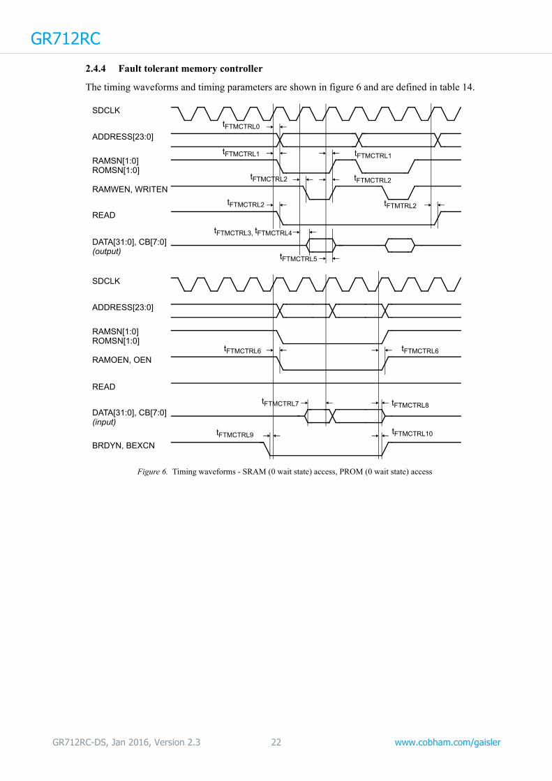
2.4.4 Fault tolerant memory controllerThe timing waveforms and timing parameters are shown in figure 6 and are defined in table 14.
Figure 6. Timing waveforms - SRAM (0 wait state) access, PROM (0 wait state) access
tFTMCTRL0
ADDRESS[23:0]
SDCLK
tFTMCTRL1
DATA[31:0], CB[7:0](output)
DATA[31:0], CB[7:0](input)
RAMSN[1:0]
tFTMCTRL3, tFTMCTRL4
READ
RAMWEN, WRITEN
tFTMCTRL9
BRDYN, BEXCN
tFTMCTRL10
tFTMCTRL2 tFTMCTRL2
tFTMCTRL6 tFTMCTRL6
ADDRESS[23:0]
SDCLK
RAMSN[1:0]
tFTMCTRL7 tFTMCTRL8
tFTMCTRL5
tFTMCTRL1
ROMSN[1:0]
ROMSN[1:0]
READ
tFTMCTRL2 tFTMTRL2
RAMOEN, OEN
GR712RC-DS, Jan 2016, Version 2.3 22 www.cobham.com/gaisler
GR712RC
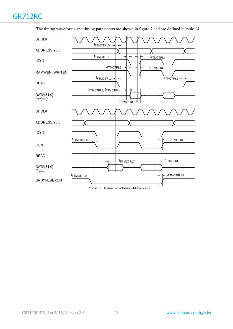
The timing waveforms and timing parameters are shown in figure 7 and are defined in table 14.Figure 7. Timing waveforms - I/O accesses
tFTMCTRL0
ADDRESS[23:0]
SDCLK
tFTMCTRL1
DATA[31:0](output)
DATA[31:0](input)
IOSN
tFTMCTRL3, tFTMCTRL4
OEN
RAMWEN, WRITEN
tFTMCTRL9
BRDYN, BEXCN
tFTMCTRL10
tFTMCTRL2 tFTMCTRL2
tFTMCTRL6 tFTMCTRL6
ADDRESS[23:0]
SDCLK
IOSN
tFTMCTRL7 tFTMCTRL8
tFTMCTRL5
tFTMCTRL1
tFTMCTRL2 tFTMCTRL2
READ
READ
GR712RC-DS, Jan 2016, Version 2.3 23 www.cobham.com/gaisler

GR712RC
Table 14. Timing parameters (VDD = 1.8V +/- 0.15V, VDDIO = 3.3V +/- 0.3V, Tcase = -55°C to +125°C)
Name Parameter Reference edge 2) Min Max Unit
tFTMCTRL0 address clock to output delay 3) rising SDCLK edge 0 1) 7.5 ns
tFTMCTRL1 clock to RAMSN[1:0] and
ROMSN[1:0]output delay 3)rising SDCLK edge 0 1) 7.5 ns
tFTMCTRL1 clock to IOSN output delay 3) rising SDCLK edge 0 1) 8.5 ns
tFTMCTRL2 clock to output delay rising SDCLK edge 0 1) 8.5 ns
tFTMCTRL3 clock to data output delay rising SDCLK edge 0 1) 6.5 ns
tFTMCTRL4 clock to data non-tri-state delay rising SDCLK edge 0 1) 6.5 ns
tFTMCTRL5 clock to data tri-state delay 4) rising SDCLK edge 0 1) 6.5 1) ns
tFTMCTRL6 clock to output delay rising SDCLK edge 0 1) 8.5 ns
tFTMCTRL7 data input to clock setup rising SDCLK edge 6.9 - ns
tFTMCTRL8 data input from clock hold rising SDCLK edge -0.5 1) - ns
tFTMCTRL9 input to clock setup rising SDCLK edge 6.9 - ns
tFTMCTRL10 input from clock hold rising SDCLK edge -0.5 1) - ns
Note 1: Parameter not measured during production test.
Note 2: The specified timing is valid for the default programmable internal clock delay of value 0.
Note 3: The ADDRESS[23:0] and RAMSN[1:0] signals change in the same clock cycle, which might not be compatible with all SRAM types. Check your SRAM documentation for compatibility.
Note 4: GR712RC does not provide internal pull-up resistors on the DATA[31:0] and CB[15:0] buses. In the case of prolonged periods of idle bus activity in a board design, i.e. high impedance state, it is advised to add external pull-up resistors.
GR712RC-DS, Jan 2016, Version 2.3 24 www.cobham.com/gaisler

GR712RC
The timing waveforms and timing parameters are shown in figure 8 and are defined in table 15.The timing waveforms and timing parameters are shown in figure 9 and are defined in table 16.
Table 15. Timing parameters (VDD = 1.8V +/- 0.15V, VDDIO = 3.3V +/- 0.3V, Tcase = -55°C to +125°C)
Name Parameter Reference edge 2) Min Max Unit
tFTMCTRL11 clock to output delay rising SDCLK edge 1 1) 6 ns
tFTMCTRL12 clock to data output delay rising SDCLK edge 1 1) 6.5 ns
tFTMCTRL13 data clock to data tri-state delay rising SDCLK edge 1 1) 6.5 1) ns
tFTMCTRL14 data input to clock setup rising SDCLK edge 6.9 - ns
tFTMCTRL15 data input from clock hold rising SDCLK edge -0.5 1) - ns
Note 1: Parameter not measured during production test.
Note 2: The specified timing is valid for the default programmable internal clock delay of value 0.
Note 3: The maximum operating frequency of the GR712RC may be limited due to the timing performance of external SDRAM devices.
Table 16. Timing parameters (VDD = 1.65V, VDDIO = 3.0V, Tcase = +125°C) 1)
Name Parameter Reference Min Max Unit
TSDCLK0 clock to output delay, delay value 0 rising INCLK edge 7 10 ns
TSDCLK51 clock to output delay, delay value 51 rising INCLK edge 16 25 ns
Note 1: Production test performed at fixed voltage and temperature without DLL enabled.
Figure 8. Timing waveforms - SDRAM accesses
SDCASN, SDRASN
SDCLK
SDWEN, SDCSN[1:0]SDDQM[3:0]
write nop read nop nop term nop nop nop
ADDRESS[16:2]
DATA[31:0], CB[15:0]
tFTMCTRL14
tFTMCTRL11
tFTMCTRL11
tFTMCTRL13tFTMCTRL12
tFTMCTRL15
Figure 9. Timing waveforms
INCLKTSDCLK0, TSDCLK51
SDCLK
GR712RC-DS, Jan 2016, Version 2.3 25 www.cobham.com/gaisler

GR712RC
2.4.5 JTAG Debug InterfaceThe timing waveforms and timing parameters are shown in figure 10 and are defined in table 17.
2.4.6 General Purpose Timer Unit
The timing waveforms and timing parameters are shown in figure 11 and are defined in table 18.
Table 17. Timing parameters (VDD = 1.8V +/- 0.15V, VDDIO = 3.3V +/- 0.3V, Tcase = -55°C to +125°C)
Name Parameter Reference edge Min Max Unit
tAHBJTAG0 clock period - 100 - ns
tAHBJTAG1 clock low/high period - 40 - ns
tAHBJTAG2 data input to clock setup rising TCK edge 10 1) - ns
tAHBJTAG3 data input from clock hold rising TCK edge 10 1) - ns
tAHBJTAG4 clock to data output delay falling TCK edge 0 1) 21 ns
Note 1: Parameter not measured during production test.
Note 2: For correct operation, all JTAG signals should be pulled-up externally with 1 - 10 kOhm. This is in line with the TAP specification where TMS and TDI implementation should be such that if an exter-nal signal fails (e.g. open circuit) then the behavior of TMS and TDI should be equivalent to a logi-cal 1 input. GR712RC does not include any internal pull-up resistors.
Table 18. Timing parameters (VDD = 1.8V +/- 0.15V, VDDIO = 3.3V +/- 0.3V, Tcase = -55°C to +125°C)
Name Parameter Reference edge Min Max Unit
tGPTIMER0 clock to output delay rising INCLK edge 2 1) 23 2) ns
tGPTIMER1 clock to output tri-state rising INCLK edge 50 1) ns
Note 1: Parameter is not measured during production test. Defined without DLL enabled.
Note 2: Parameter measured during production test without DLL enabled.
Note 3: For correct operation, the signal should be pulled-up externally with 1 - 10 kOhm. GR712RC does not include any internal pull-up resistors.
Note 4: WDOGN output is undefined during internal reset when DLL is used to generate the internal system clock frequency. See section 2.4.2 for detailed timing information on the reset behavior.
Figure 10. Timing waveforms
TDI, TMS
TCK
TDO
tAHBJTAG3tAHBJTAG4
tAHBJTAG2
tAHBJTAG0 tAHBJTAG1
Figure 11. Timing waveforms
tGPTIMER0WDOGN
INCLK
tGPTIMER1
GR712RC-DS, Jan 2016, Version 2.3 26 www.cobham.com/gaisler

GR712RC
2.4.7 General Purpose Input Output PortThe timing waveforms and timing parameters are shown in figure 12 and are defined in table 19.
2.4.8 UART Serial Interface
The timing waveforms and timing parameters are shown in figure 13 and are defined in table 20.
Table 19. Timing parameters (VDD = 1.8V +/- 0.15V, VDDIO = 3.3V +/- 0.3V, Tcase = -55°C to +125°C)
Name Parameter Reference edge Min Max Unit
tGRGPIO0 clock to output delay rising INCLK edge 2 1) 21 2) ns
tGRGPIO1 clock to non-tri-state delay rising INCLK edge 2 1) 21 1) ns
tGRGPIO2 clock to tri-state delay rising INCLK edge 50 1) ns
tGRGPIO3 input to clock hold rising INCLK edge - - ns 3)
tGRGPIO4 input to clock setup rising INCLK edge - - ns 3)
Note 1: Parameter is not measured during production test. Defined without DLL enabled.
Note 2: Parameter measured during production test without DLL enabled.
Note 3: The GPIO[...] inputs are re-synchronized to the internal system clock with a TCLK period.
Table 20. Timing parameters (VDD = 1.8V +/- 0.15V, VDDIO = 3.3V +/- 0.3V, Tcase = -55°C to +125°C)
Name Parameter Reference edge Min Max Unit
tAPBUART0 clock to output delay rising INCLK edge 2 1) 21 2) ns
tAPBUART1 input to clock hold rising INCLK edge - - ns 3)
tAPBUART2 input to clock setup rising INCLK edge - - ns 3)
Note 1: Parameter is not measured during production test. Defined without DLL enabled.
Note 2: Parameter measured during production test without DLL enabled.
Note 3: The UART_RX[5:0] inputs are re-synchronized to the internal system clock with a TCLK period.
Figure 12. Timing waveforms
tGRGPIO0GPIO[...]
INCLK
tGRGPIO0
tGRGPIO1
GPIO[...]
tGRGPIO2
tGRGPIO3GPIO[...] tGRGPIO4
(output)
(output)
(input)
Figure 13. Timing waveforms
tAPBUART0UART_TX[5:0]
INCLK
tAPBUART0
tAPBUART1UART_RX[5:0] tAPBUART2
GR712RC-DS, Jan 2016, Version 2.3 27 www.cobham.com/gaisler

GR712RC
2.4.9 SpaceWire InterfaceThe timing waveforms and timing parameters are shown in figure 14 and are defined in table 21.
SPWCLK
TSPWCLK
SPW_TXD[5:0]
SPW_TXS[5:0]
tSPW2
tSPW2
tSPW2
SPW_TXD[5:0]
SPW_TXS[5:0]
tSPW3
Figure 14. Timing waveforms
SPW_RXD[5:0]
SPW_RXS[5:0]
tSPW4, tSPW6
tSPW4, tSPW6
tSPW4, tSPW6
SPW_RXD[5:0]
SPW_RXS[5:0]
tSPW5
GR712RC-DS, Jan 2016, Version 2.3 28 www.cobham.com/gaisler

GR712RC
Table 21. Timing parameters transmitter (VDD = 1.8V +/- 0.15V, VDDIO = 3.3V +/- 0.3V, Tcase = -55°C to +125°C)Name Parameter Reference edge Min Max Unit
TSPWCLK input clock period without DLL 5) SPWCLK 10 4) - ns
FSPWCLK input clock frequency without DLL 2) SPWCLK - 100 4) MHz
DCSPWCLK input frequency duty cycle without DLL 5) SPWCLK 45 55 %
TSPWCLK input clock period with DLL x2 1) 6) SPWCLK 20 22 4) ns
FSPWCLK input clock frequency with DLL x2 1) 2) SPWCLK 45 4) 50 MHz
TSPWCLK input clock period with DLL x4 1) 6) SPWCLK 20 22 4) ns
FSPWCLK input clock frequency with DLL x4 1) 2) SPWCLK 45 4) 50 MHz
DCSPWCLK input frequency duty cycle with DLL SPWCLK 35 4) 65 4) %
TSPW internal transmitter clock period 6) - 5 500 4) ns
FSPW internal transmitter clock frequency 2) 6) - 2 4) 200 MHz
tSPW2 output data bit period - 5 4) 500 4) ns
tSPW3 data & strobe output skew & jitter - - 500 4) ps
tSPW4 input data bit period - 5 4) 500 4) ns
tSPW5 data & strobe input skew, jitter & hold - - 800 4) ps
tSPW6 data & strobe edge separation 5) - 2500 4) - ps
Note 1: For the internal SpaceWire clock, the DLL provides a times 2 or 4 multiplication of the input fre-quency.
Note 2: TSPWCLK = 1/FSPWCLK, TSPW = 1/FSPW
Note 3: N/A
Note 4: Parameter not measured during production test.
Note 5: Minimum internal edge separation equals half the internal transmitter clock period. Minimum tSPW6 is
specified at minimum TSPW with 50% duty cycle. External edge separation should not be less than the
sum of tSPW5 + tSPW6.
Note 6: The maximum SpaceWire clock frequency is specified by the parameters TSPW and FSPW.
The parameters TSPWCLK and FSPWCLK specify what the clock input pin and the DLL can support, and
not what the internal logic can support.
Note 7: The parameters tSPWn are only valid between signals belonging to one SpaceWire link.
GR712RC-DS, Jan 2016, Version 2.3 29 www.cobham.com/gaisler
GR712RC
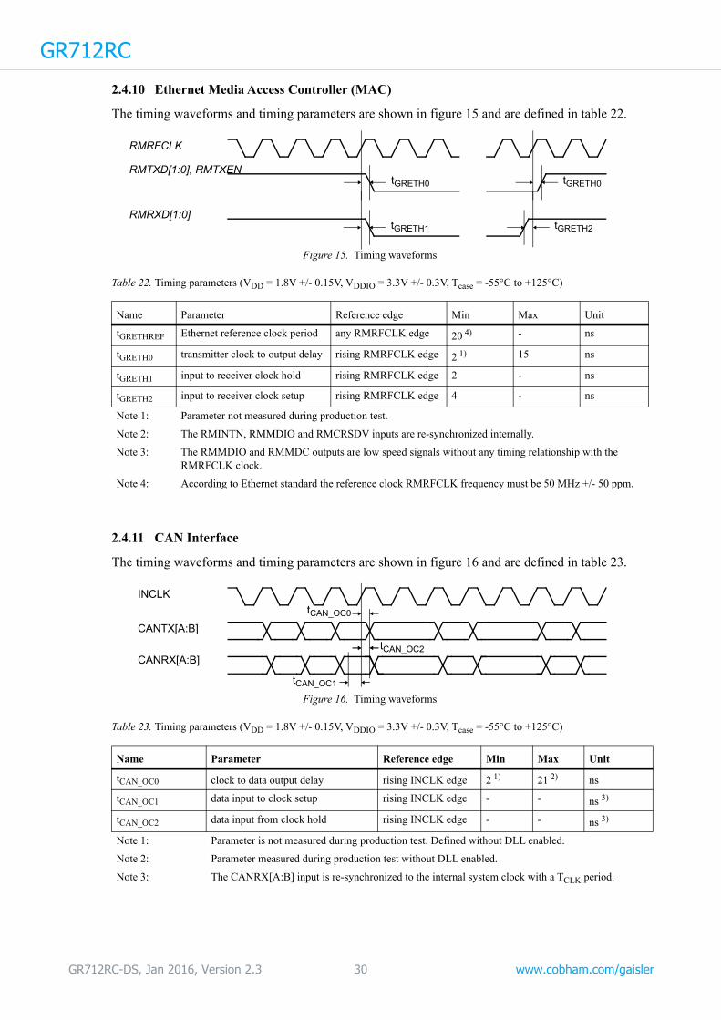
2.4.10 Ethernet Media Access Controller (MAC)The timing waveforms and timing parameters are shown in figure 15 and are defined in table 22.
2.4.11 CAN Interface
The timing waveforms and timing parameters are shown in figure 16 and are defined in table 23.
Table 22. Timing parameters (VDD = 1.8V +/- 0.15V, VDDIO = 3.3V +/- 0.3V, Tcase = -55°C to +125°C)
Name Parameter Reference edge Min Max Unit
tGRETHREF Ethernet reference clock period any RMRFCLK edge 20 4) - ns
tGRETH0 transmitter clock to output delay rising RMRFCLK edge 2 1) 15 ns
tGRETH1 input to receiver clock hold rising RMRFCLK edge 2 - ns
tGRETH2 input to receiver clock setup rising RMRFCLK edge 4 - ns
Note 1: Parameter not measured during production test.
Note 2: The RMINTN, RMMDIO and RMCRSDV inputs are re-synchronized internally.
Note 3: The RMMDIO and RMMDC outputs are low speed signals without any timing relationship with the RMRFCLK clock.
Note 4: According to Ethernet standard the reference clock RMRFCLK frequency must be 50 MHz +/- 50 ppm.
Table 23. Timing parameters (VDD = 1.8V +/- 0.15V, VDDIO = 3.3V +/- 0.3V, Tcase = -55°C to +125°C)
Name Parameter Reference edge Min Max Unit
tCAN_OC0 clock to data output delay rising INCLK edge 2 1) 21 2) ns
tCAN_OC1 data input to clock setup rising INCLK edge - - ns 3)
tCAN_OC2 data input from clock hold rising INCLK edge - - ns 3)
Note 1: Parameter is not measured during production test. Defined without DLL enabled.
Note 2: Parameter measured during production test without DLL enabled.
Note 3: The CANRX[A:B] input is re-synchronized to the internal system clock with a TCLK period.
Figure 15. Timing waveforms
tGRETH0
RMTXD[1:0], RMTXEN
RMRFCLK
tGRETH0
tGRETH1 tGRETH2
RMRXD[1:0]
Figure 16. Timing waveforms
tCAN_OC0
CANTX[A:B]
INCLK
CANRX[A:B]tCAN_OC2
tCAN_OC1
GR712RC-DS, Jan 2016, Version 2.3 30 www.cobham.com/gaisler

GR712RC
2.4.12 ObsoleteProprietary function not supported.
2.4.13 MIL-STD-1553B BC/RT/BM
The timing waveforms and timing parameters are shown in figure 17 and are defined in table 24.
Table 24. Timing parameters (VDD = 1.8V +/- 0.15V, VDDIO = 3.3V +/- 0.3V, Tcase = -55°C to +125°C)
Name Parameter Reference edge Min Max Unit
t1553BRM0 clock to data output delay rising 1553CK edge 2 1) 21 1) ns
t1553BRM1 data input to clock setup rising 1553CK edge - - ns 2)
t1553BRM2 data input from clock hold rising 1553CK edge - - ns 2)
t1553BRM3 clock frequency 1553CK 16, 20, 24 MHz 3)
Note 1: Parameter not measured during production test.
Note 2: The 1553RXA, 1553RXAN, 1553RXB and 1553RXBN inputs are re-synchronized internally.
Note 3: The core frequency must be lower than the internal system frequency: t1553BRM3 < FCLK
Figure 17. Timing waveforms
t1553BRM0
1553TXA/TXAN
1553CK
1553RXA/RXAN
t1553BRM2
t1553BRM11553RXB/RXBN
1553TXB/TXBN1553TXINHA, 1553TXINHB1553RXENA, 1553RXENB
GR712RC-DS, Jan 2016, Version 2.3 31 www.cobham.com/gaisler

GR712RC
2.4.14 I2C-masterThe timing waveforms and timing parameters are shown in figure 18 and are defined in table 25.
2.4.15 SPI controller
The timing waveforms and timing parameters are shown in figure 19 and are defined in table 26.
Table 25. Timing parameters (VDD = 1.8V +/- 0.15V, VDDIO = 3.3V +/- 0.3V, Tcase = -55°C to +125°C)
Name Parameter Reference edge Min Max Unit
tI2C0 data output valid before clock rising I2CSCL edge - scaler 1) TCLK periods
tI2C1 data output valid after clock falling I2CSCL edge scaler 1) - TCLK periods
tI2C2 data input setup to clock rising I2CSCL edge 2 2) - TCLK periods
tI2C3 data input hold from clock falling I2CSCL edge 0 2) - TCLK periods
Note 1: The core’s I2C bus functional timing depends on the core’s scaler value and the internal system clock TCLK period. When the scaler is set for the core to operate in Fast- or Standard-Mode, the timing charac-
teristics in the I2C-bus specification apply. The maximum TCLK period for proper operation is 50 ns.
Note 2: The I2CSCL and I2CSDA inputs are re-synchronized to the internal system clock with a TCLK period.
Note 3: I2CSCL and I2CSDA are open-drain outputs, driving a logical 0 level or tri-state.
Note 4: For correct operation, the signals should be pulled-up externally with 10 kOhm. GR712RC does not include any internal pull-up resistors.
Table 26. Timing parameters (VDD = 1.8V +/- 0.15V, VDDIO = 3.3V +/- 0.3V, Tcase = -55°C to +125°C)
Name Parameter Reference edge Min Max Unit
tSPICTRL0 clock to output delay driving SPICLK edge -15 2) 15 2) ns 1)
tSPICTRL1 input to clock hold sampling SPICLK edge 0 2) - ns 3)
tSPICTRL2 input to clock setup sampling SPICLK edge 20 2) - ns 3)
Note 1: The driving and sampling edges of the interface are programmable, and always opposite to each other.
Note 2: Parameter not measured during production test.
Note 3: The SPIMISO input is re-synchronized to the internal system clock with a TCLK period.
Figure 18. Timing waveforms
tI2C0
I2CSDA
I2CSCL
I2CSDAtI2C3
tI2C2
tI2C1
(output)
(input)
(input/output)
Figure 19. Timing waveforms
tSPICTRL0SPIMOSI
SPICLK
tSPICTRL0
tSPICTRL1SPIMISO tSPICTRL2
GR712RC-DS, Jan 2016, Version 2.3 32 www.cobham.com/gaisler
GR712RC
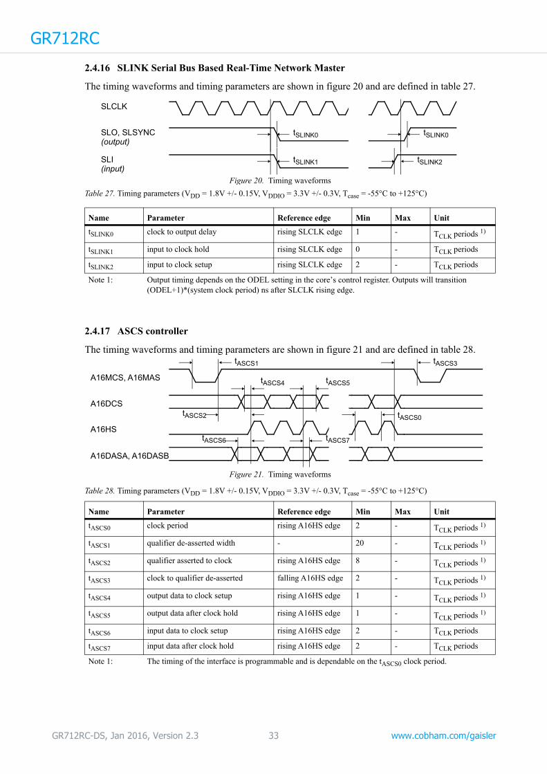
2.4.16 SLINK Serial Bus Based Real-Time Network MasterThe timing waveforms and timing parameters are shown in figure 20 and are defined in table 27.
2.4.17 ASCS controller
The timing waveforms and timing parameters are shown in figure 21 and are defined in table 28.
Table 27. Timing parameters (VDD = 1.8V +/- 0.15V, VDDIO = 3.3V +/- 0.3V, Tcase = -55°C to +125°C)
Name Parameter Reference edge Min Max Unit
tSLINK0 clock to output delay rising SLCLK edge 1 - TCLK periods 1)
tSLINK1 input to clock hold rising SLCLK edge 0 - TCLK periods
tSLINK2 input to clock setup rising SLCLK edge 2 - TCLK periods
Note 1: Output timing depends on the ODEL setting in the core’s control register. Outputs will transition (ODEL+1)*(system clock period) ns after SLCLK rising edge.
Table 28. Timing parameters (VDD = 1.8V +/- 0.15V, VDDIO = 3.3V +/- 0.3V, Tcase = -55°C to +125°C)
Name Parameter Reference edge Min Max Unit
tASCS0 clock period rising A16HS edge 2 - TCLK periods 1)
tASCS1 qualifier de-asserted width - 20 - TCLK periods 1)
tASCS2 qualifier asserted to clock rising A16HS edge 8 - TCLK periods 1)
tASCS3 clock to qualifier de-asserted falling A16HS edge 2 - TCLK periods 1)
tASCS4 output data to clock setup rising A16HS edge 1 - TCLK periods 1)
tASCS5 output data after clock hold rising A16HS edge 1 - TCLK periods 1)
tASCS6 input data to clock setup rising A16HS edge 2 - TCLK periods
tASCS7 input data after clock hold rising A16HS edge 2 - TCLK periods
Note 1: The timing of the interface is programmable and is dependable on the tASCS0 clock period.
Figure 20. Timing waveforms
tSLINK0SLO, SLSYNC
SLCLK
tSLINK0
tSLINK1SLI tSLINK2
(output)
(input)
Figure 21. Timing waveforms
tASCS0
A16MCS, A16MAS
tASCS1
tASCS2
A16DCS
A16HS
A16DASA, A16DASB
tASCS3
tASCS4 tASCS5
tASCS7tASCS6
GR712RC-DS, Jan 2016, Version 2.3 33 www.cobham.com/gaisler
GR712RC
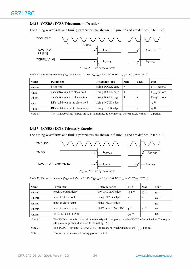
2.4.18 CCSDS / ECSS Telecommand DecoderThe timing waveforms and timing parameters are shown in figure 22 and are defined in table 29.
2.4.19 CCSDS / ECSS Telemetry Encoder
The timing waveforms and timing parameters are shown in figure 23 and are defined in table 30.
Table 29. Timing parameters (VDD = 1.8V +/- 0.15V, VDDIO = 3.3V +/- 0.3V, Tcase = -55°C to +125°C)
Name Parameter Reference edge Min Max Unit
tGRTC0 bit period rising TCCLK edge 7 - TCLK periods
tGRTC1 data/active input to clock hold rising TCCLK edge 3 - TCLK periods
tGRTC2 data/active input to clock setup rising TCCLK edge 3 - TCLK periods
tGRTC3 RF available input to clock hold rising INCLK edge - - ns 1)
tGRTC4 RF available input to clock setup rising INCLK edge - - ns 1)
Note 1: The TCRFAVL[4:0] inputs are re-synchronized to the internal system clock with a TCLK period.
Table 30. Timing parameters (VDD = 1.8V +/- 0.15V, VDDIO = 3.3V +/- 0.3V, Tcase = -55°C to +125°C)
Name Parameter Reference edge Min Max Unit
tGRTM0 clock to output delay any TMCLKO edge -15 3) 15 3) ns 1)
tGRTM1 input to clock hold rising INCLK edge - - ns 2)
tGRTM2 input to clock setup rising INCLK edge - - ns 2)
tGRTM3 input to output delay TMCLKI to TMCLKO 0 3) 23 3) ns
tGRTM4 TMCLKI clock period - 20 3) ns
Note 1: The TMDO signal is output simultaneously with the programmable TMCLKO clock edge. The oppo-site clock edge should be used for sampling TMDO.
Note 2: The TCACT[4:0] and TCRFAVL[4:0] inputs are re-synchronized to the TCLK period.
Note 3: Parameter not measured during production test.
Figure 22. Timing waveforms
TCCLK[4:0]
tGRTC1TCACT[4:0] tGRTC2TCD[4:0]
TCRFAVL[4:0]tGRTC3 tGRTC4
tGRTC0
Figure 23. Timing waveforms
tGRTM0TMDO
TMCLKO
tGRTM0
tGRTM1TCACT[4:0], TCRFAVL[4:0] tGRTM2
GR712RC-DS, Jan 2016, Version 2.3 34 www.cobham.com/gaisler

GR712RC
3 Mechanical description3.1 Package
Ceramic hermetically sealed CQFP-240L package with 0.5 mm lead pitch, with gold plated leads.
See drawing in section 3.3.
All devices are marked on top lid with GR712RC. For space class marking see the product specifica-tion [PS].
Lead trimming and forming are performed by customer prior to assembly on printed circuit board.
3.2 Pin assignment
The pin assignment in table 31 shows the implementation characteristics of each signal, indicating how each pin has been configured in terms of drive capability, polarity and reset value.
Table 31. Pin assignment
Pin no. Pin name Dir. Drive Polarity Reset value Note
1 SWMX[3] In - I/O Switch Matrix 3
2 SWMX[2] Out Slow - High I/O Switch Matrix 2
3 SWMX[1] In - I/O Switch Matrix 1
4 SWMX[0] Out Slow - High I/O Switch Matrix 0
5 CB[6] In/Out Slow - High-Z Check Bit 6
6 VDDIO I/O Supply Voltage
7 GNDIO 2) I/O Supply Ground
8 CB[5] In/Out Slow - High-Z Check Bit 5
9 CB[4] In/Out Slow - High-Z Check Bit 4
10 CB[3] In/Out Slow - High-Z Check Bit 3
11 CB[2] In/Out Slow - High-Z Check Bit 2
12 CB[1] In/Out Slow - High-Z Check Bit 1
13 VDD Core Supply Voltage
14 GND Core Supply Ground
15 CB[0] In/Out Slow - High-Z Check Bit 0
16 DATA[31] In/Out Slow - High-Z Data Bit 31
17 DATA[30] In/Out Slow - High-Z Data Bit 30
18 VDDIO I/O Supply Voltage
19 GNDIO I/O Supply Ground
20 DATA[29] In/Out Slow - High-Z Data Bit 29
21 DATA[28] In/Out Slow - High-Z Data Bit 28
22 DATA[27] In/Out Slow - High-Z Data Bit 27
23 DATA[26] In/Out Slow - High-Z Data Bit 26
24 DATA[25] In/Out Slow - High-Z Data Bit 25
25 DATA[24] In/Out Slow - High-Z Data Bit 24
26 DATA[23] In/Out Slow - High-Z Data Bit 23
27 DATA[22] In/Out Slow - High-Z Data Bit 22
28 VDDIO I/O Supply Voltage
29 GNDIO I/O Supply Ground
30 VDD Core Supply Voltage
31 GND Core Supply Ground
32 DATA[21] In/Out Slow - High-Z Data Bit 21
33 DATA[20] In/Out Slow - High-Z Data Bit 20
34 DATA[19] In/Out Slow - High-Z Data Bit 19
35 DATA[18] In/Out Slow - High-Z Data Bit 18
GR712RC-DS, Jan 2016, Version 2.3 35 www.cobham.com/gaisler

GR712RC
36 DATA[17] In/Out Slow - High-Z Data Bit 17
37 DATA[16] In/Out Slow - High-Z Data Bit 16
38 VDDIO I/O Supply Voltage
39 GNDIO I/O Supply Ground
40 DATA[15] In/Out Slow - High-Z Data Bit 15
41 DATA[14] In/Out Slow - High-Z Data Bit 14
42 DATA[13] In/Out Slow - High-Z Data Bit 13
43 DATA[12] In/Out Slow - High-Z Data Bit 12
44 DATA[11] In/Out Slow - High-Z Data Bit 11
45 DATA[10] In/Out Slow - High-Z Data Bit 10
46 DATA[9] In/Out Slow - High-Z Data Bit 9
47 VDD Core Supply Voltage
48 GND Core Supply Ground
49 DATA[8] In/Out Slow - High-Z Data Bit 8
50 VDDIO I/O Supply Voltage
51 GNDIO I/O Supply Ground
52 DATA[7] In/Out Slow - High-Z Data Bit 7
53 DATA[6] In/Out Slow - High-Z Data Bit 6
54 DATA[5] In/Out Slow - High-Z Data Bit 5
55 DATA[4] In/Out Slow - High-Z Data Bit 4
56 DATA[3] In/Out Slow - High-Z Data Bit 3
57 DATA[2] In/Out Slow - High-Z Data Bit 2
58 DATA[1] In/Out Slow - High-Z Data Bit 1
59 DATA[0] In/Out Slow - High-Z Data Bit 0
60 VDDIO I/O Supply Voltage
61 GNDIO I/O Supply Ground
62 ADDRESS[0] Out Slow - Low Address Bit 0
63 ADDRESS[1] Out Slow - Low Address Bit 1
64 ADDRESS[2] Out Fast - Low Address Bit 2
65 ADDRESS[3] Out Fast - Low Address Bit 3
66 VDD Core Supply Voltage
67 GND Core Supply Ground
68 ADDRESS[4] Out Fast - Low Address Bit 4
69 VDDIO I/O Supply Voltage
70 GNDIO I/O Supply Ground
71 ADDRESS[5] Out Fast - Low Address Bit 5
72 ADDRESS[6] Out Fast - Low Address Bit 6
73 ADDRESS[7] Out Fast - Low Address Bit 7
74 ADDRESS[8] Out Fast - Low Address Bit 8
75 VDDIO I/O Supply Voltage
76 GNDIO I/O Supply Ground
77 ADDRESS[9] Out Fast - Low Address Bit 9
78 VDD Core Supply Voltage
79 GND Core Supply Ground
80 ADDRESS[10] Out Fast - Low Address Bit 10
81 ADDRESS[11] Out Fast - Low Address Bit 11
82 ADDRESS[12] Out Fast - Low Address Bit 12
83 VDDIO I/O Supply Voltage
84 GNDIO I/O Supply Ground
85 ADDRESS[23] Out Slow - Low Address Bit 23
86 ADDRESS[13] Out Fast - Low Address Bit 13
Table 31. Pin assignment
Pin no. Pin name Dir. Drive Polarity Reset value Note
GR712RC-DS, Jan 2016, Version 2.3 36 www.cobham.com/gaisler

GR712RC
87 ADDRESS[22] Out Slow - Low Address Bit 22
88 ADDRESS[21] Out Slow - Low Address Bit 21
89 ADDRESS[14] Out Fast - Low Address Bit 14
90 VDD Core Supply Voltage
91 GND Core Supply Ground
92 ADDRESS[20] Out Slow - Low Address Bit 20
93 VDDIO I/O Supply Voltage
94 GNDIO I/O Supply Ground
95 ADDRESS[19] Out Slow - Low Address Bit 19
96 ADDRESS[15] Out Fast - Low Address Bit 15
97 ADDRESS[18] Out Slow - Low Address Bit 18
98 ADDRESS[16] Out Fast - Low Address Bit 16
99 ADDRESS[17] Out Slow - Low Address Bit 17
100 SCANEN In High Scan enable (tie to ground)
101 ROMSN[0] Out Slow Low High PROM Select 0
102 VDD Core Supply Voltage
103 GND Core Supply Ground
104 VDDIO I/O Supply Voltage
105 GNDIO I/O Supply Ground
106 ROMSN[1] Out Slow Low High PROM Select 1
107 WRITEN Out Slow Low High Write Strobe for PROM, I/O
108 IOSN Out Slow Low High I/O Select
109 RAMSN[0] Out Slow Low High SRAM Select 0
110 RAMSN[1] Out Slow Low High SRAM Select 1
111 RAMOEN Out Slow Low High SRAM Output Enable
112 RAMWEN Out Slow Low High SRAM Write Enable
113 BRDYN In Low Bus Ready
114 VDD Core Supply Voltage
115 GND Core Supply Ground
116 VDDIO I/O Supply Voltage
117 GNDIO I/O Supply Ground
118 BEXCN In Low Bus Exception
119 WDOGN Out Slow Low High-Z Watchdog Indicator (output is driven active low, else it is in tri-state and therefore requires external pull-up)
120 READ Out Slow High High SRAM, PROM, I/O read indicator
121 TDI In - Jtag Test Data In
122 TCK In - Jtag Test Clock
123 TMS In High Jtag Test Mode Select
124 TDO Out Slow - Low Jtag Test Data Out
125 TESTEN In High Test Enable (tie to ground)
126 OEN Out Slow Low High Output Enable for PROM, I/O
127 SWMX[66] In/Out Slow - High-Z I/O Switch Matrix 66
128 SWMX[65] In/Out Slow - High-Z I/O Switch Matrix 65
129 SWMX[64] In/Out Slow - High-Z I/O Switch Matrix 64
130 VDDIO I/O Supply Voltage
131 GNDIO I/O Supply Ground
132 SWMX[63] In/Out Slow - High-Z I/O Switch Matrix 63
133 VDD Core Supply Voltage
134 GND Core Supply Ground
135 SWMX[62] In/Out Slow - High-Z I/O Switch Matrix 62
136 SWMX[61] In/Out Slow - High-Z I/O Switch Matrix 61
137 SWMX[60] In/Out Slow - High-Z I/O Switch Matrix 60
Table 31. Pin assignment
Pin no. Pin name Dir. Drive Polarity Reset value Note
GR712RC-DS, Jan 2016, Version 2.3 37 www.cobham.com/gaisler
GR712RC
138 VDDIO I/O Supply Voltage
139 GNDIO I/O Supply Ground
140 SWMX[59] In/Out Slow - High-Z I/O Switch Matrix 59
141 CB[7] In/Out Slow - High-Z Check Bit 7
142 SWMX[58] In/Out Slow - High-Z I/O Switch Matrix 58
143 SWMX[57] In/Out Slow - High-Z I/O Switch Matrix 57
144 SWMX[56] In - I/O Switch Matrix 56
145 RESETN In Low System Reset
146 ERRORN Out Slow Low High-Z Processor Error Mode (output is driven active low, else it is in tri-state and therefore requires external pull-up). See a more detailed description of LEON3 integer unit exceptions in the section named “Exceptions” in [UM]
147 DLLBPN In Low DLL Bypass
148 INCLK In - Input Clock
149 VDDIO I/O Supply Voltage
150 VDD Core Supply Voltage
151 GND Core Supply Ground
152 GNDIO I/O Supply Ground
153 SWMX[55] In - I/O Switch Matrix 55
154 SWMX[54] In/Out Fast - High-Z I/O Switch Matrix 54
155 SWMX[53] In/Out Fast - High-Z I/O Switch Matrix 53
156 SDCLK Out Fast - - SDRAM Clock
157 SWMX[52] In/Out Fast - High-Z I/O Switch Matrix 52
158 VDDIO I/O Supply Voltage
159 GNDIO I/O Supply Ground
160 SWMX[51] In - I/O Switch Matrix 51
161 SWMX[50] In - I/O Switch Matrix 50
162 SWMX[49] In/Out Fast - High-Z I/O Switch Matrix 49
163 SWMX[48] In/Out Fast - High-Z I/O Switch Matrix 48
164 SWMX[47] In - I/O Switch Matrix 47
165 SWMX[46] In - I/O Switch Matrix 46
166 SWMX[45] In/Out Slow - High-Z I/O Switch Matrix 45 1)
167 VDD Core Supply Voltage
168 GND Core Supply Ground
169 SWMX[44] In/Out Slow - High-Z I/O Switch Matrix 44
170 VDDIO I/O Supply Voltage
171 GNDIO I/O Supply Ground
172 SWMX[43] In/Out Slow - High-Z I/O Switch Matrix 43 1)
173 SWMX[42] In - I/O Switch Matrix 42
174 SWMX[41] In/Out Slow - High-Z I/O Switch Matrix 41
175 SWMX[40] In/Out Slow - High-Z I/O Switch Matrix 40 1)
176 SWMX[39] In - I/O Switch Matrix 39
177 SWMX[38] In - I/O Switch Matrix 38
178 SWMX[37] In/Out Slow - High-Z I/O Switch Matrix 37 1)
179 SWMX[36] In/Out Slow - High-Z I/O Switch Matrix 36
180 VDDIO I/O Supply Voltage
181 GNDIO I/O Supply Ground
182 SWMX[35] In - I/O Switch Matrix 35
183 SWMX[34] In - I/O Switch Matrix 34
184 SWMX[33] In/Out Slow - High-Z I/O Switch Matrix 33
185 SWMX[32] In/Out Slow - High-Z I/O Switch Matrix 32
186 VDD Core Supply Voltage
Table 31. Pin assignment
Pin no. Pin name Dir. Drive Polarity Reset value Note
GR712RC-DS, Jan 2016, Version 2.3 38 www.cobham.com/gaisler
GR712RC
187 GND Core Supply Ground
188 SWMX[31] In - I/O Switch Matrix 31
189 SWMX[30] In - I/O Switch Matrix 30
190 SWMX[29] In/Out Slow - High-Z I/O Switch Matrix 29
191 SWMX[28] In/Out Slow - High-Z I/O Switch Matrix 28
192 SWMX[27] In - I/O Switch Matrix 27
193 SWMX[26] In - I/O Switch Matrix 26
194 VDDIO I/O Supply Voltage
195 GNDIO I/O Supply Ground
196 SWMX[25] In/Out Fast - High-Z I/O Switch Matrix 25
197 SWMX[24] In/Out Fast - High-Z I/O Switch Matrix 24
198 VDD Core Supply Voltage
199 GND Core Supply Ground
200 SWMX[23] In - I/O Switch Matrix 23
201 SWMX[22] In - I/O Switch Matrix 22
202 SWMX[21] In/Out Fast - High-Z I/O Switch Matrix 21
203 SWMX[20] In/Out Fast - High-Z I/O Switch Matrix 20
204 SPW_RXD[1] - SpaceWire Receive Data 1
205 SPW_RXS[1] - SpaceWire Receive Strobe 1
206 SPW_TXD[1] Out Fast - Low SpaceWire Transmit Data 1
207 VDDIO I/O Supply Voltage
208 GNDIO I/O Supply Ground
209 SPW_TXS[1] Out Fast - Low SpaceWire Transmit Strobe 1
210 VDD Core Supply Voltage
211 GND Core Supply Ground
212 SPWCLK In - SpaceWire Receiver and Transmitter Clock
213 SPW_RXD[0] In - SpaceWire Receive Data 0
214 SPW_RXS[0] In - SpaceWire Receive Strobe 0
215 SPW_TXD[0] Out Fast - Low SpaceWire Transmit Data 0
216 SPW_TXS[0] Out Fast - Low SpaceWire Transmit Strobe 0
217 SWMX[19] In Slow - I/O Switch Matrix 19
218 SWMX[18] In - I/O Switch Matrix 18
219 SWMX[17] In/Out Fast - High-Z I/O Switch Matrix 17
220 SWMX[16] In/Out Fast - High-Z I/O Switch Matrix 16
221 VDDIO I/O Supply Voltage
222 VDD Core Supply Voltage
Table 31. Pin assignment
Pin no. Pin name Dir. Drive Polarity Reset value Note
GR712RC-DS, Jan 2016, Version 2.3 39 www.cobham.com/gaisler

GR712RC
223 GND Core Supply Ground
224 GNDIO I/O Supply Ground
225 SWMX[15] In - I/O Switch Matrix 15
226 SWMX[14] In - I/O Switch Matrix 14
227 SWMX[13] In/Out Fast - High-Z I/O Switch Matrix 13
228 SWMX[12] In/Out Fast - High-Z I/O Switch Matrix 12
229 SWMX[11] In - I/O Switch Matrix 11
230 SWMX[10] In/Out Slow - High-Z I/O Switch Matrix 10
231 SWMX[9] In - I/O Switch Matrix 09
232 SWMX[8] In/Out Slow - High-Z I/O Switch Matrix 08
233 SWMX[7] In - I/O Switch Matrix 07
234 VDD Core Supply Voltage
235 GND Core Supply Ground
236 VDDIO I/O Supply Voltage
237 GNDIO I/O Supply Ground
238 SWMX[6] In/Out Slow - High-Z I/O Switch Matrix 06 1)
239 SWMX[5] In - I/O Switch Matrix 05
240 SWMX[4] In/Out Slow - High-Z I/O Switch Matrix 04 1)
Note 1: See tables 3 and 5 for detailed description of behavior at reset.
Note 2: GNDIO is connected internally to GND.
Table 31. Pin assignment
Pin no. Pin name Dir. Drive Polarity Reset value Note
GR712RC-DS, Jan 2016, Version 2.3 40 www.cobham.com/gaisler

GR712RC
3.3 Mechanical package drawingsFigure 24. Top view
GND
GND
VDD
VDDIO
GND
GND
VDD
VDDIO
Table 32. Dimensions
Millimeters
Min. Max.
A Total height --- 3.50
A1 Body height --- 2.75
A2 0.10 0.40
b Lead width 0.15 0.25
c Lead height 0.10 0.20
D/E 74.80 75.40
D1/E1 55.44 56.56
D2/E2 31.75 32.25
D3/E3 29.50 BSC
D4/E4 21.00 TYP
e Lead pitch 0.50 BSC
L1 16.50 TYP
Note 1: The seal ring and the lid are connected to GND.
Note 2: Package weight is 16 +/-1 grams, including the lead-frame.
GR712RC-DS, Jan 2016, Version 2.3 41 www.cobham.com/gaisler
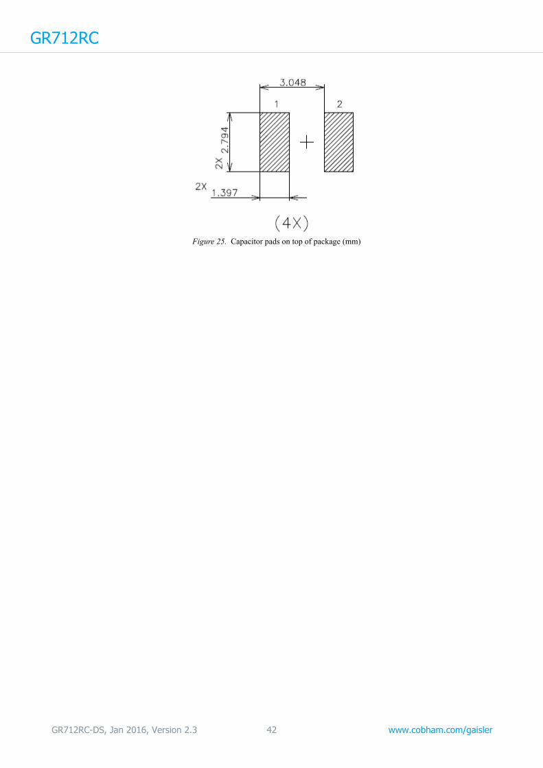
GR712RC
Figure 25. Capacitor pads on top of package (mm)
GR712RC-DS, Jan 2016, Version 2.3 42 www.cobham.com/gaisler

GR712RC
4 Reference documents[UM] GR712RC Dual-Core LEON3-FT SPARC V8 Processor - User's Manual, Cobham Gaisler, www.cobham.com/gaisler
[PS] Product Specification GR712RC, GR712RC-PS, Cobham Gaisler
[SPARC] The SPARC Architecture Manual, Version 8, Revision SAV080SI9308, SPARC International Inc.
[SPW] ECSS - Space Engineering, SpaceWire - Links, Nodes, Routers and Networks, ECSS-E-ST-50-12C, 31 July 2008
[RMAPID] ECSS - Space Engineering, SpaceWire Protocol Identification, ECSS-E-ST-50-51C, February 2010
[RMAP] ECSS - Space Engineering, Remote Memory Access Protocol, ECSS-E-ST-50-52C, February 2010
[1553BRM] Core1553BRM Product Handbook, 50200040-0/11-04, November 2004, Actel Corpo-ration
Core1553BRM MIL-STD-1553 BC, RT, and MT, 51700052-4/12.05, v 5.0, December 2005, Actel Corporation
Core1553BRM User's Guide, 50200023-0/06.04, June 2004, Actel Corporation
Core1553BRM v2.16 Release Notes, 51300019-8/6.06, June 2006, Actel Corporation
[MIL883] Test Method Standard, Microcircuits, revision H, 26 February 2010, MIL-STD-883H
[MIL38535] Integrated Circuits (Microcircuits) Manufacturing, General Specification For, revision J, 28 December 2010, MIL-PRF-38535J
GR712RC-DS, Jan 2016, Version 2.3 43 www.cobham.com/gaisler

GR712RC
5 Screening, qualification, and quality controlGR712RC is provided as a high reliability product for space, for which space level screening and qualifications tests are performed in accordance to the product specification [PS].
A Certificate of Compliance is delivered with space grade parts.
A procurement specification is provided for space grade parts.
GR712RC is also provided in prototype grade in military or commercial temperature range.
6 Ordering information
Ordering information is provided in table 33 and a legend is provided in table 34.
7 Change record
Change record information is provided in table 35.
Table 33. Ordering information, available models
Product Description
GR712RC-MS-CQ240 Flight model
GR712RC-MP-CQ240 Electrical qualification model
GR712RC-CP-CQ240 Engineering model (prototype)
Note: The -CQ240 affix was previously -CG240. There is however no change to the package. The product and qualification state is the same.
Table 34. Ordering legend
Designator Option Description
Product GR712RC Dual-core LEON3-FT SPARC V8 Processor
Temperature Range M -55°C to +125°C (Military range)
C 0°C to +70°C (Commercial range)
Screening Level S Space grade
P Prototype grade
Package Type CQ Ceramic Quad Flat Pack (CQFP) 1)
Lead Count 240 Number of leads
Note 1: Gold lead finish
Table 35. Change record
Issue Date Sections Note
2.3 2016 Jan None Updated text in footer. No other changes. Change bars pre-served from version 2.2.
2.2 2015 Nov 1.2
3.2
Maximum size and bank size for PROM, SRAM and SDRAM
Point to ERRORN description in [UM]
GR712RC-DS, Jan 2016, Version 2.3 44 www.cobham.com/gaisler
GR712RC
2.1 2014 June 1.2
2.3
2.4.4
2.4.6
2.4.7
2.4.8
2.4.11
3.2
3.3
6
Key features: TID up to 300 krad(Si)
Updated DC electrical performance characteristics
Table 16 note 1 updated
Table 18 note 1 updated
Table 19 note 1 updated
Table 20 note 1 updated
Table 23 note 1 and parameter note updated
Max load changed to drive capability in Table 31
OEN pin output drive capability specified
Table 32 note 1 updated
Part numbering updated with new affix for the package identi-fication
2.0 2013 February 1.2
1.4
2.1
2.2
2.3
2.4
2.4.1, 2.4.3, 2.4.4, 2.4.5, 2.4.6, 2.4.7, 2.4.8, 2.4.9, 2.4.10, 2.4.11, 2.4.13, 2.4.15, 2.4.19
1.5, 2.4.12
3.1
3.2
3.3
4
Key features updated
Signal descriptions clarified
Absolute maximum ratings updated
Recommended operating conditions updated
DC parameters updated
AC parameter test conditions clarified
Updated timing
Obsolete proprietary function removed
Package marking clarified
GNDIO connection to GND clarified
Weight information added
Reference to product specification added
1.5 2012 May 1.5 The following conflicts added to table:CCSDS TC 0 vs. ProprietaryCCSDS TC 0 vs. ASCSCCSDS TC 1 vs. ProprietaryCCSDS TC 1 vs. EthernetCCSDS TC 2 vs. EthernetProprietary vs. SpaceWire 2
1.4 2012 January 2.4.5 TCK edges in JTAG waveform & timing parameters corrected
1.3 2011 March 1.2, 24, 5Table 6
Timing parameters redefinedQualification level specifiedConflict between SLINK and CCSDS TC 3 clarified
1.2 2011 August 2.3 Added detailed core power consumption
1.1 2011 February Tables 3 and 5Tables 3, 4 and 19, figure 19Table 31
SDDQM signals marked as active highGPIO1/GPIO2 names changed to GPIOReference added regarding behavior at reset
1.0 2011 February All New document layoutAll pin descriptions, reset values etc. updated
Table 35. Change record
Issue Date Sections Note
GR712RC-DS, Jan 2016, Version 2.3 45 www.cobham.com/gaisler

Cobham Gaisler AB Kungsgatan 12411 19 GöteborgSwedenwww.cobham.com/[email protected]: +46 31 7758650F: +46 31 421407
Cobham Gaisler AB, reserves the right to make changes to any products and services described herein at any time without notice. Consult Cobham or an authorized sales representative to verify that the information in this document is current before using this product. Cobham does not assume any responsibility or liability arising out of the application or use of any product or service described herein, except as expressly agreed to in writing by Cobham; nor does the purchase, lease, or use of a product or service from Cobham convey a license under any patent rights, copyrights, trademark rights, or any other of the intellectual rights of Cobham or of third parties. All information is provided as is. There is no warranty that it is correct or suitable for any purpose, neither implicit nor explicit.
Copyright © 2016 Cobham Gaisler AB
GR712RC-DS, Jan 2016, Version 2.3 46 of 46 www.cobham.com/gaisler
GR712RC