gigadevice semiconductor inc. gd32f130xx cortex -m3 32-bit...
TRANSCRIPT

GigaDevice Semiconductor Inc.
GD32F130xx ARM® Cortex™-M3 32-bit MCU
Datasheet
GD32F130xx
1 / 39
Table of Contents
List of Figures ............................................................................................................................. 3
List of Tables ............................................................................................................................... 4
1 General description ......................................................................................................... 5
2 Device overview ............................................................................................................... 6 2.1 Device information .............................................................................................................................. 6
2.2 Block diagram ...................................................................................................................................... 7
2.3 Pinouts and pin assignment .............................................................................................................. 8
2.4 Memory map ...................................................................................................................................... 10
2.5 Clock tree ........................................................................................................................................... 11
2.6 Pin definitions .................................................................................................................................... 12
3 Functional description .................................................................................................. 18 3.1 ARM® Cortex™-M3 core .................................................................................................................. 18
3.2 On-chip memory ................................................................................................................................ 18
3.3 Clock, reset and supply management ........................................................................................... 19
3.4 Boot modes ........................................................................................................................................ 19
3.5 Power saving modes ........................................................................................................................ 20
3.6 Analog to digital converter (ADC) ................................................................................................... 20
3.7 DMA .................................................................................................................................................... 21
3.8 General-purpose inputs/outputs (GPIOs) ...................................................................................... 21
3.9 Timers and PWM generation ........................................................................................................... 21
3.10 Real time clock (RTC) ...................................................................................................................... 23
3.11 Inter-integrated circuit (I2C) ............................................................................................................. 23
3.12 Serial peripheral interface (SPI) ...................................................................................................... 24
3.13 Universal synchronous asynchronous receiver transmitter (USART) ....................................... 24
3.14 Debug mode ...................................................................................................................................... 24
3.15 Package and operation temperature .............................................................................................. 24
4 Electrical characteristics .............................................................................................. 25 4.1 Absolute maximum ratings .............................................................................................................. 25
4.2 Recommended DC characteristics ................................................................................................. 25
4.3 Power consumption .......................................................................................................................... 26
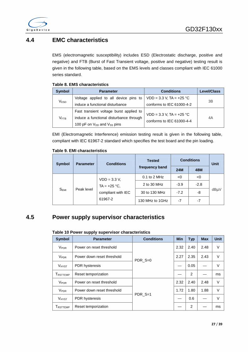
4.4 EMC characteristics .......................................................................................................................... 27
4.5 Power supply supervisor characteristics ....................................................................................... 27
4.6 Electrical sensitivity........................................................................................................................... 28
4.7 External clock characteristics .......................................................................................................... 28
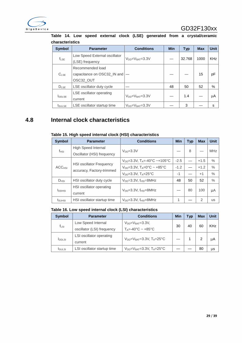
4.8 Internal clock characteristics ........................................................................................................... 29
4.9 PLL characteristics ........................................................................................................................... 30
4.10 Memory characteristics .................................................................................................................... 30
4.11 GPIO characteristics ......................................................................................................................... 30

GD32F130xx
2 / 39
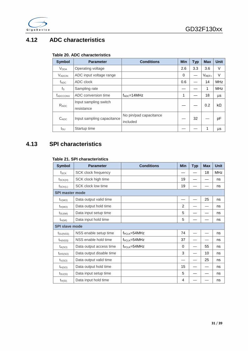
4.12 ADC characteristics .......................................................................................................................... 31
4.13 SPI characteristics ............................................................................................................................ 31
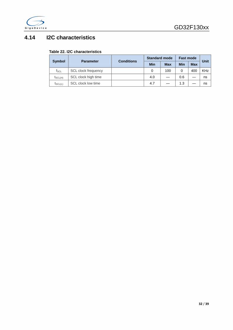
4.14 I2C characteristics ............................................................................................................................ 32
5 Package information ..................................................................................................... 33 5.1 TSSOP package outline dimensions ............................................................................................. 33
5.2 QFN package outline dimensions .................................................................................................. 34
5.3 LQFP package outline dimensions ................................................................................................ 35
6 Ordering Information ..................................................................................................... 37
7 Revision History ............................................................................................................. 38
GD32F130xx
3 / 39
List of Figures
Figure 1. GD32F130xx block diagram ...................................................................................................................... 7
Figure 3. GD32F130Rx LQFP64 pinouts ................................................................................................................. 8
Figure 4. GD32F130Cx LQFP48 pinouts ................................................................................................................. 8
Figure 5. GD32F130Gx QFN28 pinouts ................................................................................................................... 9
Figure 6. GD32F130Fx TSSOP20 pinouts .............................................................................................................. 9
Figure 7. GD32F130xx memory map ..................................................................................................................... 10
Figure 8. GD32F130xx clock tree ............................................................................................................................ 11
Figure 9. TSSOP package outline ........................................................................................................................... 33
Figure 10. QFN package outline.............................................................................................................................. 34
Figure 11. LQFP package outline ............................................................................................................................ 35
GD32F130xx
4 / 39
List of Tables
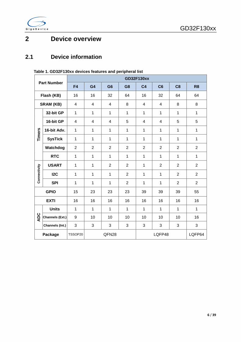
Table 1. GD32F130xx devices features and peripheral list ................................................................................... 6
Table 2. GD32F130xx pin definitions ...................................................................................................................... 12
Table 3. Port A alternate functions summary ........................................................................................................ 16
Table 4. Port B alternate functions summary ........................................................................................................ 17
Table 5. Absolute maximum ratings ........................................................................................................................ 25
Table 6. DC operating conditions ............................................................................................................................ 25
Table 7. Power consumption characteristics ......................................................................................................... 26
Table 8. EMS characteristics ................................................................................................................................... 27
Table 9. EMI characteristics ..................................................................................................................................... 27
Table 10 Power supply supervisor characteristics................................................................................................ 27
Table 11. ESD characteristics.................................................................................................................................. 28
Table 12. Static latch-up characteristics ................................................................................................................ 28
Table 13. High speed external clock (HSE) generated from a crystal/ceramic characteristics ...................... 28
Table 14. Low speed external clock (LSE) generated from a crystal/ceramic characteristics ....................... 29
Table 15. High speed internal clock (HSI) characteristics ................................................................................... 29
Table 16. Low speed internal clock (LSI) characteristics ..................................................................................... 29
Table 17. PLL characteristics ................................................................................................................................... 30
Table 18. Flash memory characteristics ................................................................................................................. 30
Table 19. I/O port characteristics ............................................................................................................................. 30
Table 20. ADC characteristics .................................................................................................................................. 31
Table 23. SPI characteristics .................................................................................................................................... 31
Table 22. I2C characteristics .................................................................................................................................... 32
Table 24. TSSOP20 package dimensions ............................................................................................................. 33
Table 25. QFN28 package dimensions .................................................................................................................. 34
Table 26. LQFP package dimensions ..................................................................................................................... 36
Table 27. Part ordering code for GD32F130xx devices ....................................................................................... 37
Table 28. Revision history......................................................................................................................................... 38
GD32F130xx
5 / 39
1 General description
The GD32F130xx device belongs to the value line of GD32 MCU family. It is a 32-bit general-purpose microcontroller based on the high performance ARM® Cortex™-M3 RISC core with best ratio in terms of processing power, reduced power consumption and peripheral set. The Cortex™-M3 is a next generation processor core which is tightly coupled with a Nested Vectored Interrupt Controller (NVIC), SysTick timer and advanced debug support.
The GD32F130xx device incorporates the ARM® Cortex™-M3 32-bit processor core operating at 48 MHz frequency with Flash accesses zero wait states to obtain maximum efficiency. It provides up to 64 KB on-chip Flash memory and up to 8 KB SRAM memory. An extensive range of enhanced I/Os and peripherals connected to two APB buses. The devices offer one 12-bit ADC, up to five general-purpose 16-bit timers, a general-purpose 32-bit timer, a PWM advanced-control timer, as well as standard and advanced communication interfaces: up to two SPIs, two I2Cs and two USARTs.
The device operates from a 2.6 to 3.6 V power supply and available in –40 to +85 °C temperature range. Several power saving modes provide the flexibility for maximum optimization between wakeup latency and power consumption, an especially important consideration in low power applications.
The above features make the GD32F130xx devices suitable for a wide range of applications, especially in areas such as industrial control, motor drives, user interface, power monitor and alarm systems, consumer and handheld equipment, gaming and GPS, E-bike and so on.
GD32F130xx
6 / 39
2 Device overview
2.1 Device information
Table 1. GD32F130xx devices features and peripheral list
Part Number GD32F130xx
F4 G4 G6 G8 C4 C6 C8 R8
Flash (KB) 16 16 32 64 16 32 64 64
SRAM (KB) 4 4 4 8 4 4 8 8
Tim
ers
32-bit GP 1 1 1 1 1 1 1 1
16-bit GP 4 4 4 5 4 4 5 5
16-bit Adv. 1 1 1 1 1 1 1 1
SysTick 1 1 1 1 1 1 1 1
Watchdog 2 2 2 2 2 2 2 2
RTC 1 1 1 1 1 1 1 1
Con
nect
ivity
USART 1 1 2 2 1 2 2 2
I2C 1 1 1 2 1 1 2 2
SPI 1 1 1 2 1 1 2 2
GPIO 15 23 23 23 39 39 39 55
EXTI 16 16 16 16 16 16 16 16
AD
C Units 1 1 1 1 1 1 1 1
Channels (Ext.) 9 10 10 10 10 10 10 16
Channels (Int.) 3 3 3 3 3 3 3 3
Package TSSOP20 QFN28 LQFP48 LQFP64

GD32F130xx
7 / 39
2.2 Block diagram
Figure 1. GD32F130xx block diagram
ICode
DC
odeSystemNVIC
TPIU SW
FlashMemory
Controller
FlashMemory
AH
B Matrix
SRAMController SRAM
AHB to APB Bridge 2
GP DMA 7chs
USART1
SPI1
ADC
TM17
12-bitSAR ADC
IBus
ARM Cortex-M3 Processor
Fmax: 48MHz
POR/PDR
PLLFmax: 72MHz
LDO1.2V
HSI8MHz
HSE4-32MHz
LVD
EXTIPowered by VDD/VDDA
TM1
AHB1: Fmax = 48MHz
AHB to APB Bridge 1CRC RST/CLK
Controller
DBus
AHB2: Fmax = 48MHz GPIO PortsA, B, C, D, F
HSI1414MHz
SYS Config
TM15
TM16
APB2: F
max = 48M
Hz
LSI40KHz
Powered by LDO (1.2V)
WWDG
APB1: Fm
ax = 48MH
z
SPI2
USART2
I2C1
I2C2
RTC
IWDG
PWR
TM14
TM3
TM2
GD32F130xx
8 / 39
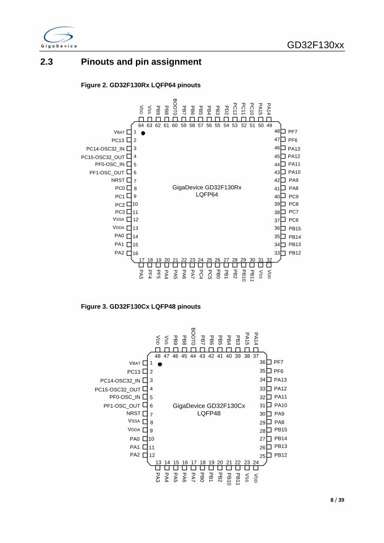
2.3 Pinouts and pin assignment
Figure 2. GD32F130Rx LQFP64 pinouts
4
13
1415
17 18 19 20 21 22 23 24 25 26 27 28
64 63 62 61 60 59 58 57 56 55 54 53
VSSA
PA1
PA12PA11PA10PA9PA8
PC9PC8PC7
PC6
PB15
PB14PB13
PA3
PF4
PF5
PA6
PA7
PC4
PC5
PB0PB1
PB2
VD
D
VSS
PB9
PB8
PB7
PB6
BOO
T0
PB5
PB4
PB3
PD2
PC12
GigaDevice GD32F130RxLQFP64
29 30 31 32
PB10
PB11
VSS
PA13
52 51 50 49PA15
PA14
1
23
VBAT
PC13
PC14-OSC32_IN
PC15-OSC32_OUT
NRST
PA0
48
47
46
45
444342
414039
383736
3534
56
789
10
1112
16PA2 PB1233
VD
D
PC0
PC1
PC2PC3
VDDA
PC10
PC11
PF1-OSC_OUT
PF0-OSC_IN
PA5
PA4
PF6
PF7
Figure 3. GD32F130Cx LQFP48 pinouts
4
13 14 15 16 17 18 19 20 21 22 23 24
48 47 46 45 44 43 42 41 40 39 38 37
VSSA
PA1
PA12PA11PA10PA9PA8PB15
PB14PB13
PA
3
PA
4
PA
5
PA
6
PA
7
PB
0
PB
1
PB
2
VD
D
VS
S
PB
9
PB
8
PB
7
PB
6
BO
OT0
PB
5
PB
4
PB
3
GigaDevice GD32F130CxLQFP48
PB
10
PB
11
VS
S
PF6PA13
PA
15
PA
14
1
23
VBAT
PC13
PC14-OSC32_IN
PC15-OSC32_OUT
NRST
PA0
36
35
34
33
323130
292827
2625
56
789
10
1112PA2 PB12
VD
D
VDDA
PF1-OSC_OUT
PF0-OSC_IN
PF7

GD32F130xx
9 / 39
Figure 4. GD32F130Gx QFN28 pinouts
4 PA8
PB1
PA
2P
A3
PA
4P
A5
PA
6P
A7
PB
0
PB
5P
B4
PB
3
PA
14GigaDevice
GD32F130xxQFN28
PA9
123
NRST
PA0567
VDDA
8 9 10 11 12 13 14
18
212019
171615
28 27 26 25 24 23 22
OSC_OUT/PF1OSC_IN/PF0
BOOT0
VSS
PA1
VDD
PA10
PA13
PA
15
PB
7P
B6
Figure 5. GD32F130Fx TSSOP20 pinouts
PA5
GigaDevice GD32F130Fx
TSSOP20
PA6
NRST
PA0VDDA
OSC_OUT/PF1OSC_IN/PF0
BOOT0
PA1
VDD
PA7
PA9
PA2
PA10PA13PA14
PA3PA4
PB1Vss
1
2
3
4
5
6
7
8
9
10
20
19
18
17
16
15
14
13
12
11

GD32F130xx
10 / 39
2.4 Memory map
Figure 6. GD32F130xx memory map
Cortex-M3 Internal Peripherals
Peripherals
SRAM
0xFFFF FFFF
0xE010 0000
0xE000 0000
0xC000 0000
0xA000 0000
0x8000 0000
0x6000 0000
0x4000 0000
0x2000 0000
0x0000 0000
7
6
5
4
3
2
1
0
reserved
reserved
reserved
reserved
reserved
reserved
reserved
reserved
reserved
reserved
Aliased to Flash or system memory according to BOOT pins configuration
System memory
Option Bytes
Flash memory
0x1FFF FFFF
0x1FFF F80F
0x1FFF F800
0x1FFF EC00
0x0801 FFFF
0x0800 0000
0x0000 0000 TM20x4000 0000
TM30x4000 04000x4000 0800
reserved0x4000 1000
reserved0x4000 1400
reserved0x4000 2000
TM140x4000 2400
reserved0x4000 2800
RTC0x4000 2C00
WWDG0x4000 3000
IWDG0x4000 3400
reserved0x4000 3800
SPI20x4000 3C00
reserved0x4000 4000
reserved0x4000 4400
USART20x4000 4800
reserved0x4000 5400
I2C10x4000 5800
I2C20x4000 5C00
reserved0x4000 6000
reserved0x4000 6400
reserved0x4000 7000
PWR0x4000 7400
reserved0x4000 7800
reserved0x4000 7C00
reserved0x4000 C000
reserved0x4000 C400
reserved0x4001 0000
SYS Config0x4001 0400
EXTI0x4001 0800
reserved0x4001 2400
ADC0x4001 2800
reserved0x4001 2C00
TM10x4001 3000
SPI10x4001 3400
reserved0x4001 3800
USART10x4001 3C00
reserved0x4001 4000
TM150x4001 4400
TM160x4001 4800
TM170x4001 4C00
reserved0x4002 0000
DMA0x4002 0400
reserved0x4002 1000
RCC0x4002 1400
reserved0x4002 2000
Flash Interface0x4002 2400
reserved0x4002 3000
CRC0x4002 3400
reserved0x4002 4000
reserved0x4002 4400
reserved0x4800 0000
Port A0x4800 0400
Port B0x4800 0800
Port C0x4800 0C00
Port D0x4800 1000
reserved0x4800 1400
Port F0x4800 1800
reserved0x5000 0000
0x5000 0000

GD32F130xx
11 / 39
2.5 Clock tree
Figure 7. GD32F130xx clock tree
/2
4-32 MHzHSE XTAL
8 MHzHSI RC PLL
ClockMonitor
PLLSELHSEPREDV
PLLEN
0
1
00
01
10
CK_HSI
CK_HSE
CK_PLLCK_SYS
48 MHz max
AHBPrescaler÷1,2...512
CK_AHB48 MHz max
APB1Prescaler
÷1,2,4,8,16
TIM2,3,6,14÷[apb1
prescaler/2]
APB2Prescaler
÷1,2,4,8,16
TIM1,15,16,17
÷[apb2 prescaler/2]
ADCPrescaler
÷2,4,8,12,16
CK_APB2
48 MHz max
Peripheral enable
PCLK2
to APB2 peripherals
CK_APB1
48 MHz max
Peripheral enable
PCLK1
to APB1 peripherals
TIM1 enable
CK_TIM1
to TIM1,15,16,17
TIMX enable
CK_TIMX
to TIM2,3,6,14
CK_ADCX to ADC1
14 MHz max
AHB enableHCLK
(to AHB bus,Cortex-M3,SRAM,DMA)
FLITF enable(by hardware)
CK_FLITF
(to FLITF)
÷8CK_CST
(to Cortex-M3 SysTick)FCLK
(free running clock)
32.768 KHzLSE OSC
11
10
01
40 KHzLSI RC
CK_RTC
CK_IWDG
(to RTC)
(to IWDG)
/32
CK_LSE
CK_PLLCK_HSECK_HSI
CK_OUT
SCS[1:0]
RTCSRC[1:0]
÷1,2...16
1
0
ADCSEL
14 MHzHSI RC
11
00
01
10
CK_HSI
CK_LSE
CK_SYS
CK_USART1
to USART1
CK_SYS
CK_LSICK_HSI14
0
*1,2
÷1,2,4...128
CKOUTDIV
Legend: HSE = High speed external clock HSI = High speed internal clock LSE = Low speed external clock LSI = Low speed internal clock

GD32F130xx
12 / 39
2.6 Pin definitions
Table 2. GD32F130xx pin definitions
Pin Name
Pins
Pin
Type
(1)
I/O(2
) Lev
el
Functions description
LQFP
64
LQFP
48
QFN
28
TSSO
P20
VBAT 1 1 - - P
Default: VBAT
PC13-TAMPE
R-RTC 2 2 - - I/O
Default: PC13 Additional: RTC_TAMP1, RTC_TS, RTC_OUT, WKUP2
PC14-OSC32
_IN 3 3 - - I/O
Default: PC14 Additional: OSC32_IN
PC15-
OSC32_OUT 4 4 - - I/O
Default: PC15 Additional: OSC32_OUT
PF0-OSC_IN 5 5 2 2 I/O 5VT Default: PF0 Additional: OSC_IN
PF1-OSC_O
UT 6 6 3 3 I/O 5VT
Default: PF1 Additional: OSC_OUT
NRST 7 7 4 4 I/O
Default: NRST
PC0 8 - - - I/O
Default: PC0 Alternate: EVENTOUT Additional: ADC_IN10
PC1 9 - - - I/O
Default: PC1 Alternate: EVENTOUT Additional: ADC_IN11
PC2 10 - - - I/O
Default: PC2 Alternate: EVENTOUT Additional: ADC_IN12
PC3 11 - - - I/O
Default: PC3 Alternate: EVENTOUT Additional: ADC_IN13
VSSA 12 8 - - P
Default: VSSA
VDDA 13 9 5 5 P
Default: VDDA
PA0-WKUP 14 10 6 6 I/O
Default: PA0 Alternate: USART1_CTS(3), USART2_CTS(4), TM2_CH1_ETR, I2C2_SCL Additional: ADC_IN0, RTC_TAMP2, WKUP1
PA1 15 11 7 7 I/O
Default: PA1 Alternate: USART1_RTS(3), USART2_RTS(4), TM2_CH2, I2C2_SDA, EVENTOUT Additional: ADC_IN1
PA2 16 12 8 8 I/O
Default: PA2 Alternate: USART1_TX(3), USART2_TX(4), TM2_CH3, TM15_CH1 , Additional: ADC_IN2
PA3 17 13 9 9 I/O
Default: PA3

GD32F130xx
13 / 39
Pin Name
Pins
Pin
Type
(1)
I/O(2
) Lev
el
Functions description LQ
FP64
LQFP
48
QFN
28
TSSO
P20
Alternate: USART1_RX(3), USART2_RX(4), TM2_CH4, TM15_CH2 Additional: ADC_IN3
PF4 18 - - - I/O 5VT Default: PF4 Alternate: SPI2_NSS, EVENTOUT
PF5 19 - - - I/O 5VT Default: PF5 Alternate: EVENTOUT
PA4 20 14 10 10 I/O
Default: PA4 Alternate: SPI1_NSS, USART1_RX(3), USART2_RX(4), TM14_CH1, SPI2_NSS Additional: ADC_IN4
PA5 21 15 11 11 I/O
Default: PA5 Alternate: SPI1_SCK, TM2_CH1_ETR Additional: ADC_IN5
PA6 22 16 12 12 I/O
Default: PA6 Alternate: SPI1_MISO, TM3_CH1, TM1_BKIN, TM16_CH1, EVENTOUT Additional: ADC_IN6
PA7 23 17 13 13 I/O
Default: PA7 Alternate: SPI1_MOSI, TM3_CH2, TM14_CH1, TM1_CH1N, TM17_CH1, EVENTOUT Additional: ADC_IN7
PC4 24 - - - I/O
Default: PC4 Alternate: EVENTOUT Additional: ADC_IN14
PC5 25 - - - I/O
Default: PC5 Additional: ADC_IN15
PB0 26 18 14 - I/O
Default: PB0 Alternate: TM3_CH3, TM1_CH2N, USART2_RX, EVENTOUT Additional: ADC_IN8
PB1 27 19 15 14 I/O
Default: PB1 Alternate: TM3_CH4, TM14_CH1, TM1_CH3N, SPI2_SCK Additional: ADC_IN9
PB2 28 20 - - I/O 5VT Default: PB2
PB10 29 21 - - I/O 5VT Default: PB10 Alternate: I2C2_SCL, TM2_CH3
PB11 30 22 - - I/O 5VT Default: PB11 Alternate: I2C2_SDA, TM2_CH4, EVENTOUT
VSS 31 23 16 15 P
Default: VSS
VDD 32 24 17 16 P
Default: VDD
PB12 33 25 - - I/O 5VT
Default: PB12 Alternate: SPI1_NSS(3), SPI2_NSS(4), TM1_BKIN, I2C2_SMBA,
EVENTOUT
PB13 34 26 - - I/O 5VT Default: PB13
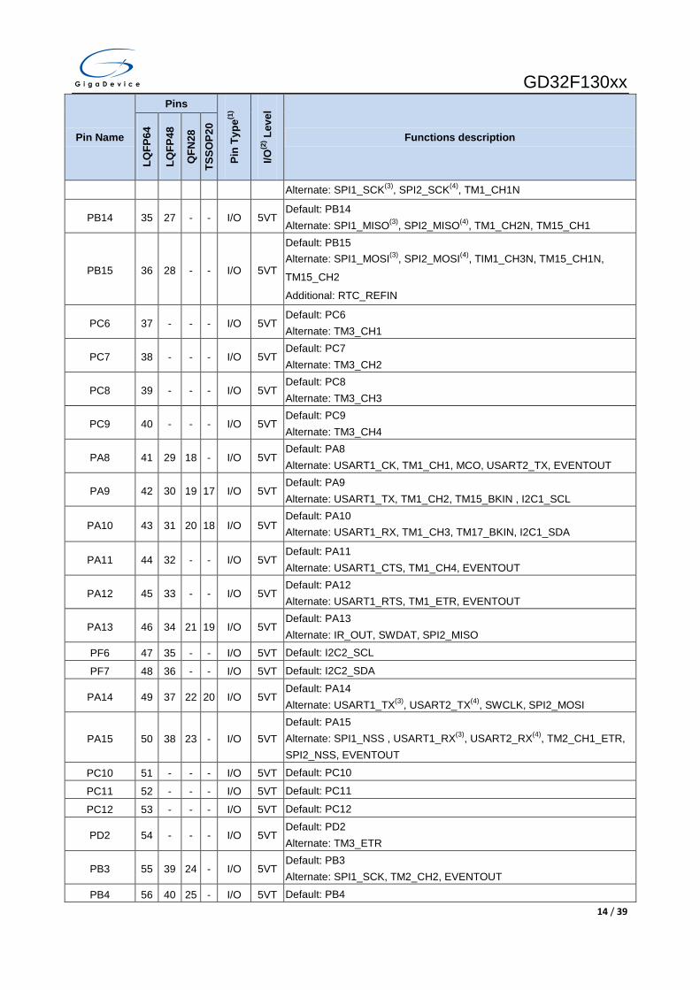
GD32F130xx
14 / 39
Pin Name
Pins
Pin
Type
(1)
I/O(2
) Lev
el
Functions description LQ
FP64
LQFP
48
QFN
28
TSSO
P20
Alternate: SPI1_SCK(3), SPI2_SCK(4), TM1_CH1N
PB14 35 27 - - I/O 5VT Default: PB14 Alternate: SPI1_MISO(3), SPI2_MISO(4), TM1_CH2N, TM15_CH1
PB15 36 28 - - I/O 5VT
Default: PB15 Alternate: SPI1_MOSI(3), SPI2_MOSI(4), TIM1_CH3N, TM15_CH1N,
TM15_CH2
Additional: RTC_REFIN
PC6 37 - - - I/O 5VT Default: PC6 Alternate: TM3_CH1
PC7 38 - - - I/O 5VT Default: PC7 Alternate: TM3_CH2
PC8 39 - - - I/O 5VT Default: PC8 Alternate: TM3_CH3
PC9 40 - - - I/O 5VT Default: PC9 Alternate: TM3_CH4
PA8 41 29 18 - I/O 5VT Default: PA8 Alternate: USART1_CK, TM1_CH1, MCO, USART2_TX, EVENTOUT
PA9 42 30 19 17 I/O 5VT Default: PA9 Alternate: USART1_TX, TM1_CH2, TM15_BKIN , I2C1_SCL
PA10 43 31 20 18 I/O 5VT Default: PA10 Alternate: USART1_RX, TM1_CH3, TM17_BKIN, I2C1_SDA
PA11 44 32 - - I/O 5VT Default: PA11 Alternate: USART1_CTS, TM1_CH4, EVENTOUT
PA12 45 33 - - I/O 5VT Default: PA12 Alternate: USART1_RTS, TM1_ETR, EVENTOUT
PA13 46 34 21 19 I/O 5VT Default: PA13 Alternate: IR_OUT, SWDAT, SPI2_MISO
PF6 47 35 - - I/O 5VT Default: I2C2_SCL
PF7 48 36 - - I/O 5VT Default: I2C2_SDA
PA14 49 37 22 20 I/O 5VT Default: PA14 Alternate: USART1_TX(3), USART2_TX(4), SWCLK, SPI2_MOSI
PA15 50 38 23 - I/O 5VT Default: PA15 Alternate: SPI1_NSS , USART1_RX(3), USART2_RX(4), TM2_CH1_ETR, SPI2_NSS, EVENTOUT
PC10 51 - - - I/O 5VT Default: PC10
PC11 52 - - - I/O 5VT Default: PC11
PC12 53 - - - I/O 5VT Default: PC12
PD2 54 - - - I/O 5VT Default: PD2 Alternate: TM3_ETR
PB3 55 39 24 - I/O 5VT Default: PB3 Alternate: SPI1_SCK, TM2_CH2, EVENTOUT
PB4 56 40 25 - I/O 5VT Default: PB4
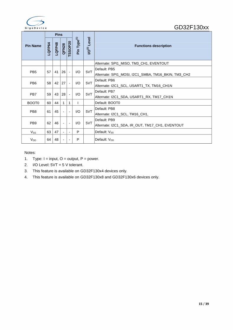
GD32F130xx
15 / 39
Pin Name
Pins
Pin
Type
(1)
I/O(2
) Lev
el
Functions description LQ
FP64
LQFP
48
QFN
28
TSSO
P20
Alternate: SPI1_MISO, TM3_CH1, EVENTOUT
PB5 57 41 26 - I/O 5VT Default: PB5 Alternate: SPI1_MOSI, I2C1_SMBA, TM16_BKIN, TM3_CH2
PB6 58 42 27 - I/O 5VT Default: PB6 Alternate: I2C1_SCL, USART1_TX, TM16_CH1N
PB7 59 43 28 - I/O 5VT Default: PB7 Alternate: I2C1_SDA, USART1_RX, TM17_CH1N
BOOT0 60 44 1 1 I
Default: BOOT0
PB8 61 45 - - I/O 5VT Default: PB8 Alternate: I2C1_SCL, TM16_CH1,
PB9 62 46 - - I/O 5VT Default: PB9 Alternate: I2C1_SDA, IR_OUT, TM17_CH1, EVENTOUT
VSS 63 47 - - P Default: VSS
VDD 64 48 - - P Default: VDD
Notes: 1. Type: I = input, O = output, P = power. 2. I/O Level: 5VT = 5 V tolerant. 3. This feature is available on GD32F130x4 devices only. 4. This feature is available on GD32F130x8 and GD32F130x6 devices only.
GD32F130xx
16 / 39
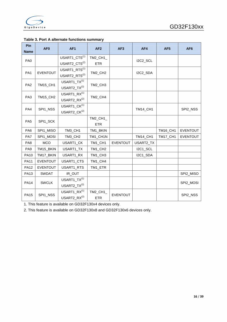
Table 3. Port A alternate functions summary
Pin
Name AF0 AF1 AF2 AF3 AF4 AF5 AF6
PA0 USART1_CTS(1)
USART2_CTS(2)
TM2_CH1_
ETR I2C2_SCL
PA1 EVENTOUT USART1_RTS(1)
USART2_RTS(2) TM2_CH2 I2C2_SDA
PA2 TM15_CH1 USART1_TX(1)
USART2_TX(2) TM2_CH3
PA3 TM15_CH2 USART1_RX(1)
USART2_RX(2) TM2_CH4
PA4 SPI1_NSS USART1_CK(1)
USART2_CK(2) TM14_CH1 SPI2_NSS
PA5 SPI1_SCK TM2_CH1_
ETR
PA6 SPI1_MISO TM3_CH1 TM1_BKIN TM16_CH1 EVENTOUT
PA7 SPI1_MOSI TM3_CH2 TM1_CH1N TM14_CH1 TM17_CH1 EVENTOUT
PA8 MCO USART1_CK TM1_CH1 EVENTOUT USART2_TX
PA9 TM15_BKIN USART1_TX TM1_CH2 I2C1_SCL
PA10 TM17_BKIN USART1_RX TM1_CH3 I2C1_SDA
PA11 EVENTOUT USART1_CTS TM1_CH4
PA12 EVENTOUT USART1_RTS TM1_ETR
PA13 SWDAT IR_OUT SPI2_MISO
PA14 SWCLK USART1_TX(1)
USART2_TX(2) SPI2_MOSI
PA15 SPI1_NSS USART1_RX(1)
USART2_RX(2)
TM2_CH1_
ETR EVENTOUT SPI2_NSS
1. This feature is available on GD32F130x4 devices only. 2. This feature is available on GD32F130x8 and GD32F130x6 devices only.

GD32F130xx
17 / 39
Table 4. Port B alternate functions summary Pin
Name AF0 AF1 AF2 AF3 AF4 AF5 AF6
PB0 EVENTOUT TM3_CH3 TM1_CH2N USART2_RX
PB1 TM14_CH1 TM3_CH4 TM1_CH3N SPI2_SCK
PB2
PB3 SPI1_SCK EVETOUT TM2_CH2
PB4 SPI1_MISO TM3_CH1 EVENTOUT
PB5 SPI1_MOSI TM3_CH2 TM16_BKIN I2C1_SMBA
PB6 USART1_TX I2C1_SCL TM16_CH1N
PB7 USART1_RX I2C1_SDA TM17_CH1N
PB8 I2C1_SCL TM16_CH1
PB9 IR_OUT I2C1_SDA TM17_CH1 EVENTOUT
PB10 I2C2_SCL TM2_CH3
PB11 EVENTOUT I2C2_SDA TM2_CH4
PB12 SPI1_NSS(1)
SPI2_NSS(2) EVENTOUT TM1_BKIN I2C2_SMBA
PB13 SPI1_SCK(1)
SPI2_SCK(2) TM1_CH1N
PB14 SPI1_MISO(1)
SPI2_MISO(2) TM15_CH1 TM1_CH2N
PB15 SPI1_MOSI(1)
SPI2_MOSI(2) TM15_CH2 TM1_CH3N TM15_CH1N
1. This feature is available on GD32F130x4 devices only. 2. This feature is available on GD32F130x8 and GD32F130x6 devices only.

GD32F130xx
18 / 39
3 Functional description
3.1 ARM® Cortex™-M3 core
The Cortex™-M3 processor is the latest generation of ARM® processors for embedded systems. It has been developed to provide a low-cost platform that meets the needs of MCU implementation, with a reduced pin count and low-power consumption, while delivering outstanding computational performance and an advanced system response to interrupts. 32-bit ARM® Cortex™-M3 processor core Up to 48 MHz operation frequency Single-cycle multiplication and hardware divider Integrated Nested Vectored Interrupt Controller (NVIC) 24-bit SysTick timer
The Cortex™-M3 processor is based on the ARMv7 architecture and supports both Thumb and Thumb-2 instruction sets. Some system peripherals listed below are also provided by Cortex™-M3: Internal Bus Matrix connected with ICode bus, DCode bus, system bus, Private
Peripheral Bus (PPB) and debug accesses (AHB-AP) Nested Vectored Interrupt Controller (NVIC) Flash Patch and Breakpoint (FPB) Data Watchpoint and Trace (DWT) Instrument Trace Macrocell (ITM) Serial Wire JTAG Debug Port (SWJ-DP) Trace Port Interface Unit (TPIU)
3.2 On-chip memory
Up to 64 Kbytes of Flash memory Up to 8 Kbytes of SRAM with hardware parity checking
The ARM® Cortex™-M3 processor is structured in Harvard architecture which can use separate buses to fetch instructions and load/store data. 64 Kbytes of inner Flash and 8 Kbytes of inner SRAM at most is available for storing programs and data, both accessed (R/W) at CPU clock speed with zero wait states. The Figure 7. GD32F130xx memory map shows the memory map of the GD32F130xx series of devices, including code, SRAM, peripheral, and other pre-defined regions.
GD32F130xx
19 / 39
3.3 Clock, reset and supply management
Internal 8 MHz factory-trimmed RC and external 4 to 32 MHz crystal oscillator Internal 40 KHz RC calibrated oscillator and external 32.768 KHz crystal oscillator Integrated system clock PLL 2.6 to 3.6 V application supply and I/Os Supply Supervisor: POR (Power On Reset), PDR (Power Down Reset), and low voltage
detector (LVD)
The Clock Control Unit (CCU) provides a range of oscillator and clock functions. These include speed internal RC oscillator and external crystal oscillator, high speed and low speed two types. Several prescalers allow the frequency configuration of the AHB and two APB domains. The maximum frequency of the AHB and two APB domains is 72 MHz. See Figure 9 for details on the clock tree.
The Reset Control Unit (RCU) controls three kinds of reset: system reset resets the processor core and peripheral IP components. Power-on reset (POR) and power-down reset (PDR) are always active, and ensures proper operation starting from 2.6 V and down to 1.8V. The device remains in reset mode when VDD is below a specified threshold. The embedded low voltage detector (LVD) monitors the power supply, compares it to the voltage threshold and generates an interrupt as a warning message for leading the MCU into security.
Power supply schemes: VDD range: 2.6 to 3.6 V, external power supply for I/Os and the internal regulator.
Provided externally through VDD pins. VSSA, VDDA range: 2.6 to 3.6 V, external analog power supplies for ADC, reset blocks,
RCs and PLL. VDDA and VSSA must be connected to VDD and VSS, respectively. VBAT range: 1.8 to 3.6 V, power supply for RTC, external clock 32 kHz oscillator and
backup registers (through power switch) when VDD is not present.
3.4 Boot modes
At startup, boot pins are used to select one of three boot options: Boot from main Flash memory (default) Boot from system memory Boot from on-chip SRAM
In default condition, boot from main Flash memory is selected. The boot loader is located in the internal boot ROM memory (system memory). It is used to reprogram the Flash memory by using USART1 in device mode.
GD32F130xx
20 / 39
3.5 Power saving modes
The MCU supports three kinds of power saving modes to achieve even lower power consumption. They are Sleep mode, Deep-sleep mode, and Standby mode. These operating modes reduce the power consumption and allow the application to achieve the best balance between the CPU operating time, speed and power consumption. Sleep mode
In sleep mode, only the clock of CPU core is off. All peripherals continue to operate and any interrupt/event can wake up the system.
Deep-sleep mode In Deep-sleep mode, all clocks in the 1.2V domain are off, and all of the high speed crystal oscillator (HSI, HSE) and PLL are disabled. Only the contents of SRAM and registers are retained. Any interrupt or wakeup event from EXTI lines can wake up the system from the Deep-sleep mode including the 16 external lines, the RTC alarm and the LVD output,. When exiting the Deep-sleep mode, the HSI is selected as the system clock.
Standby mode In Standby mode, the whole 1.2V domain is power off, the LDO is shut down, and all of HSI, HSE and PLL are disabled. The contents of SRAM and registers (except Backup Registers) are lost. There are four wakeup sources for the Standby mode, including the external reset from NRST pin, the RTC alarm, the IWDG reset, and the rising edge on WKUP pin.
3.6 Analog to digital converter (ADC)
12-bit SAR ADC engine with up to 1 MSPS conversion rate Conversion range: VSSA to VDDA (2.6 to 3.6 V) Temperature sensor
One 12-bit 1 μs multi-channel ADC is integrated in the device. It is a total of up to 16 multiplexed external channels and 3 internal channels for temperature sensor, voltage reference, VBAT voltage measurement. The conversion range is between 2.6 V < VDDA < 3.6 V. An analog watchdog block can be used to detect the channels, which are required to remain within a specific threshold window. A configurable channel management block of analog inputs also can be used to perform conversions in single, continuous, scan or discontinuous mode to support more advanced usages. The ADC can be triggered from the events generated by the general-purpose timers (TMx) and the advanced-control timers (TM1) with internal connection.
The temperature sensor can be used to generate a voltage that varies linearly with temperature. It is internally connected to the ADC_IN16 input channel which is used to convert the sensor output voltage into a digital value. Each device is factory-calibrated to improve the accuracy and the calibration data are stored in the system memory area.

GD32F130xx
21 / 39
3.7 DMA
7 channel DMA controller Peripherals supported: Timers, ADC, SPIs, I2Cs, USARTs
The flexible general-purpose DMA controllers provide a hardware method of transferring data between peripherals and/or memory without intervention from the CPU, thereby freeing up bandwidth for other system functions. Three types of access method are supported: peripheral to memory, memory to peripheral, memory to memory
Each channel is connected to fixed hardware DMA requests. The priorities of DMA channel requests are determined by software configuration and hardware channel number. Transfer size of source and destination are independent and configurable.
3.8 General-purpose inputs/outputs (GPIOs)
Up to 55 fast GPIOs, all mappable on 16 external interrupt vectors (EXTI) Analog input/output configurable Alternate function input/output configurable
There are up to 55 general purpose I/O pins (GPIO) in GD32F130xx, named PA0 ~ PA15 and PB0 ~ PB15, PC0 ~ PC15, PD2, PF0, PF1, PF4-PF7 to implement logic input/output functions. Each of the GPIO ports has related control and configuration registers to satisfy the requirements of specific applications. The external interrupts on the GPIO pins of the device have related control and configuration registers in the External Interrupt Control Unit (EXTI). The GPIO ports are pin-shared with other alternative functions (AFs) to obtain maximum flexibility on the package pins. Each of the GPIO pins can be configured by software as output (push-pull or open-drain), as input (with or without pull-up or pull-down) or as peripheral alternate function. Most of the GPIO pins are shared with digital or analog alternate functions. All GPIOs are high-current capable except for analog inputs.
3.9 Timers and PWM generation
One 16-bit advanced-control timer (TM1), one 32-bit general-purpose timer (TM2), five 16-bit general-purpose timers (TM3, TM14 ~ TM17)
Up to 4 independent channels of PWM, output compare or input capture for each general-purpose timer (GPTM) and external trigger input
16-bit, motor control PWM advanced-control timer with programmable dead-time generation for output match
Encoder interface controller with two inputs using quadrature decoder 24-bit SysTick timer down counter 2 watchdog timers (Independent watchdog and window watchdog)
The advanced-control timer (TM1) can be used as a three-phase PWM multiplexed on 6
GD32F130xx
22 / 39
channels. It has complementary PWM outputs with programmable dead-time generation. It can also be used as a complete general-purpose timer. The 4 independent channels can be used for input capture, output compare, PWM generation (edge- or center-aligned counting modes) and single pulse mode output. If configured as a general-purpose 16-bit timer, it has the same functions as the TMx timer. It can be synchronized with external signals or to interconnect with other GPTMs together which have the same architecture and features.
The general-purpose timer (GPTM) can be used for a variety of purposes including general time, input signal pulse width measurement or output waveform generation such as a single pulse generation or PWM output, up to 4 independent channels for input capture/output compare. TM2 is based on a 32-bit auto-reload up/downcounter and a 16-bit prescaler. TM3 is based on a 16-bit auto-reload up/downcounter and a 16-bit prescaler. TM14 ~ TM17 is based on a 16-bit auto-reload upcounter and a 16-bit prescaler. The GPTM also supports an encoder interface with two inputs using quadrature decoder.
The GD32F130xx have two watchdog peripherals, Independent watchdog and window watchdog. They offer a combination of high safety level, flexibility of use and timing accuracy.
The independent watchdog timer includes a 12-bit down-counting counter and a 8-bit prescaler, It is clocked from an independent 40 kHz internal RC and as it operates independently of the main clock, it can operate in stop and standby modes. It can be used either as a watchdog to reset the device when a problem occurs, or as a free-running timer for application timeout management.
The window watchdog is based on a 7-bit down counter that can be set as free-running. It can be used as a watchdog to reset the device when a problem occurs. It is clocked from the main clock. It has an early warning interrupt capability and the counter can be frozen in debug mode.
The SysTick timer is dedicated for OS, but could also be used as a standard down counter. It features: A 24-bit down counter Auto reload capability Maskable system interrupt generation when the counter reaches 0 Programmable clock source
GD32F130xx
23 / 39
3.10 Real time clock (RTC)
Independent binary-coded decimal (BCD) format timer/counter with five 32-bit backup registers.
Calendar with subsecond, seconds, minutes, hours, week day, date, year and month automatically correction
Alarm function with wake up from deep-sleep and standby mode capability On-the-fly correction for synchronization with master clock. Digital calibration with 1 ppm
resolution for compensation of quartz crystal inaccuracy.
The real time clock is an independent timer which provides a set of continuously running counters in backup registers to provide a real calendar function, and provides an alarm interrupt or an expected interrupt. It is not reset by a system or power reset, or when the device wakes up from standby mode. A 20-bit prescaler is used for the time base clock and is by default configured to generate a time base of 1 second from a clock at 32.768 kHz from external crystal oscillator.
3.11 Inter-integrated circuit (I2C)
Up to two I2C bus interfaces can support both master and slave mode with a frequency up to 400 kHz
Provide arbitration function, optional PEC (packet error checking) generation and checking
Supports 7-bit and 10-bit addressing mode and general call addressing mode
The I2C interface is an internal circuit allowing communication with an external I2C interface which is an industry standard two line serial interface used for connection to external hardware. These two serial lines are known as a serial data line (SDA) and a serial clock line (SCL). The I2C module provides two data transfer rates: 100 kHz of standard mode or 400 kHz of the fast mode. The I2C module also has an arbitration detect function to prevent the situation where more than one master attempts to transmit data to the I2C bus at the same time. A CRC-8 calculator is also provided in I2C interface to perform packet error checking for I2C data.
GD32F130xx
24 / 39
3.12 Serial peripheral interface (SPI)
Up to two SPI interfaces with a frequency of up to 18 MHz Support both master and slave mode Hardware CRC calculation and transmit automatic CRC error checking
The SPI interface uses 4 pins, among which are the serial data input and output lines (MISO & MOSI), the clock line (SCK) and the slave select line (NSS). Both SPIs can be served by the DMA controller. The SPI interface may be used for a variety of purposes, including simplex synchronous transfers on two lines with a possible bidirectional data line or reliable communication using CRC checking.
3.13 Universal synchronous asynchronous receiver transmitter (USART)
Up to two USARTs with operating frequency up to 9 MHz Supports both asynchronous and clocked synchronous serial communication modes IrDA SIR encoder and decoder support LIN break generation and detection ISO 7816-3 compliant smart card interface
The USART (USART1, USART2) are used to translate data between parallel and serial interfaces, provides a flexible full duplex data exchange using synchronous or asynchronous transfer. It is also commonly used for RS-232 standard communication. The USART includes a programmable baud rate generator which is capable of dividing the system clock to produce a dedicated clock for the USART transmitter and receiver. The USART also supports DMA function for high speed data communication.
3.14 Debug mode
Serial wire JTAG debug port (SWJ-DP)
The ARM® SWJ-DP Interface is embedded and is a combined JTAG and serial wire debug port that enables either a serial wire debug or a JTAG probe to be connected to the target.
3.15 Package and operation temperature
LQFP64 (GD32F130Rx), LQFP48 (GD32F130Cx), QFN28 (GD32F130Gx) and TSSOP20 (GD32F130Fx)
Operation temperature range: -40°C to +85°C (industrial level)
GD32F130xx
25 / 39
4 Electrical characteristics
4.1 Absolute maximum ratings
The maximum ratings are the limits to which the device can be subjected without permanently damaging the device. Note that the device is not guaranteed to operate properly at the maximum ratings. Exposure to the absolute maximum rating conditions for extended periods may affect device reliability.
Table 5. Absolute maximum ratings Symbol Parameter Min Max Unit
VDD External voltage range VSS - 0.3 VSS + 3.6 V
VDDA External analog supply voltage VSSA - 0.3 VSSA + 3.6 V
VBAT External battery supply voltage VSS - 0.3 VSS + 3.6 V
VIN Input voltage on 5V tolerant pin VSS - 0.3 VDD + 4.0 V
Input voltage on other I/O VSS - 0.3 4.0 V
IIO Maximum current for GPIO pins — 25 mA
TA Operating temperature range -40 +85 °C
TSTG Storage temperature range -55 +150 °C
TJ Maximum junction temperature — 125 °C
4.2 Recommended DC characteristics
Table 6. DC operating conditions Symbol Parameter Conditions Min Typ Max Unit
VDD Supply voltage — 2.6 3.3 3.6 V
VDDA Analog supply voltage Same as VDD 2.6 3.3 3.6 V
VBAT Battery supply voltage — 1.8 — 3.6 V
GD32F130xx
26 / 39
4.3 Power consumption
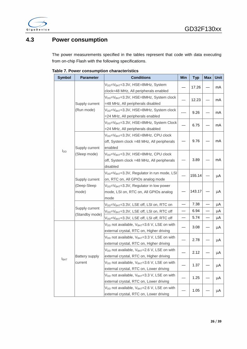
The power measurements specified in the tables represent that code with data executing from on-chip Flash with the following specifications.
Table 7. Power consumption characteristics Symbol Parameter Conditions Min Typ Max Unit
IDD
Supply current
(Run mode)
VDD=VBAT=3.3V, HSE=8MHz, System
clock=48 MHz, All peripherals enabled — 17.26 — mA
VDD=VBAT=3.3V, HSE=8MHz, System clock
=48 MHz, All peripherals disabled — 12.23 — mA
VDD=VBAT=3.3V, HSE=8MHz, System clock
=24 MHz, All peripherals enabled -— 9.26 — mA
VDD=VBAT=3.3V, HSE=8MHz, System Clock
=24 MHz, All peripherals disabled — 6.75 — mA
Supply current
(Sleep mode)
VDD=VBAT=3.3V, HSE=8MHz, CPU clock
off, System clock =48 MHz, All peripherals
enabled
— 9.76 — mA
VDD=VBAT=3.3V, HSE=8MHz, CPU clock
off, System clock =48 MHz, All peripherals
disabled
— 3.89 — mA
Supply current
(Deep-Sleep
mode)
VDD=VBAT=3.3V, Regulator in run mode, LSI
on, RTC on, All GPIOs analog mode — 155.14 — μA
VDD=VBAT=3.3V, Regulator in low power
mode, LSI on, RTC on, All GPIOs analog
mode
— 143.17 — μA
Supply current
(Standby mode)
VDD=VBAT=3.3V, LSE off, LSI on, RTC on — 7.38 — μA
VDD=VBAT=3.3V, LSE off, LSI on, RTC off — 6.94 — μA
VDD=VBAT=3.3V, LSE off, LSI off, RTC off — 5.74 — μA
IBAT Battery supply
current
VDD not available, VBAT=3.6 V, LSE on with
external crystal, RTC on, Higher driving — 3.08 — μA
VDD not available, VBAT=3.3 V, LSE on with
external crystal, RTC on, Higher driving — 2.78 — μA
VDD not available, VBAT=2.6 V, LSE on with
external crystal, RTC on, Higher driving — 2.12 — μA
VDD not available, VBAT=3.6 V, LSE on with
external crystal, RTC on, Lower driving — 1.37 — μA
VDD not available, VBAT=3.3 V, LSE on with
external crystal, RTC on, Lower driving — 1.25 — μA
VDD not available, VBAT=2.6 V, LSE on with
external crystal, RTC on, Lower driving — 1.05 — μA
GD32F130xx
27 / 39
4.4 EMC characteristics
EMS (electromagnetic susceptibility) includes ESD (Electrostatic discharge, positive and negative) and FTB (Burst of Fast Transient voltage, positive and negative) testing result is given in the following table, based on the EMS levels and classes compliant with IEC 61000 series standard.
Table 8. EMS characteristics Symbol Parameter Conditions Level/Class
VESD Voltage applied to all device pins to
induce a functional disturbance
VDD = 3.3 V, TA = +25 °C
conforms to IEC 61000-4-2 3B
VFTB
Fast transient voltage burst applied to
induce a functional disturbance through
100 pF on VDD and VSS pins
VDD = 3.3 V, TA = +25 °C
conforms to IEC 61000-4-4 4A
EMI (Electromagnetic Interference) emission testing result is given in the following table, compliant with IEC 61967-2 standard which specifies the test board and the pin loading.
Table 9. EMI characteristics
Symbol Parameter Conditions Tested
frequency band
Conditions Unit
24M 48M
SEMI Peak level
VDD = 3.3 V,
TA = +25 °C,
compliant with IEC
61967-2
0.1 to 2 MHz <0 <0
dBμV 2 to 30 MHz -3.9 -2.8
30 to 130 MHz -7.2 -8
130 MHz to 1GHz -7 -7
4.5 Power supply supervisor characteristics
Table 10 Power supply supervisor characteristics Symbol Parameter Conditions Min Typ Max Unit
VPOR Power on reset threshold
PDR_S=0
2.32 2.40 2.48 V
VPDR Power down reset threshold 2.27 2.35 2.43 V
VHYST PDR hysteresis — 0.05 — V
TRSTTEMP Reset temporization — 2 — ms
VPOR Power on reset threshold
PDR_S=1
2.32 2.40 2.48 V
VPDR Power down reset threshold 1.72 1.80 1.88 V
VHYST PDR hysteresis — 0.6 — V
TRSTTEMP Reset temporization — 2 — ms

GD32F130xx
28 / 39
4.6 Electrical sensitivity
The device is strained in order to determine its performance in terms of electrical sensitivity. Electrostatic discharges (ESD) are applied directly to the pins of the sample. Static latch-up (LU) test is based on the two measurement methods.
Table 11. ESD characteristics Symbol Parameter Conditions Min Typ Max Unit
VESD(HBM) Electrostatic discharge
voltage (human body model)
TA=25 °C;
JESD22-A114 — — 5000 V
VESD(CDM) Electrostatic discharge
voltage (charge device model)
TA=25 °C;
JESD22-C101 — — 500 V
Table 12. Static latch-up characteristics Symbol Parameter Conditions Min Typ Max Unit
LU I-test
TA=25 °C; JESD78 — — ±100 mA
Vsupply over voltage — — 5.4 V
4.7 External clock characteristics
Table 13. High speed external clock (HSE) generated from a crystal/ceramic characteristics
Symbol Parameter Conditions Min Typ Max Unit
fHSE High Speed External oscillator
(HSE) frequency VDD=3.3V 4 8 32 MHz
CHSE Recommended load capacitance
on OSC_IN and OSC_OUT — — 20 30 pF
RFHSE
Recommended external feedback
resistor between XTALIN and
XTALOUT
— — 200 — KΩ
DHSE HSE oscillator duty cycle — 48 50 52 %
IDDHSE HSE oscillator operating current VDD=3.3V, TA=25°C — 1.4 — μA
tSUHSE HSE oscillator startup time VDD=3.3V, TA=25°C — 2 — ms
GD32F130xx
29 / 39
Table 14. Low speed external clock (LSE) generated from a crystal/ceramic characteristics
Symbol Parameter Conditions Min Typ Max Unit
fLSE Low Speed External oscillator
(LSE) frequency VDD=VBAT=3.3V — 32.768 1000 KHz
CLSE
Recommended load
capacitance on OSC32_IN and
OSC32_OUT
— — — 15 pF
DLSE LSE oscillator duty cycle — 48 50 52 %
IDDLSE LSE oscillator operating
current VDD=VBAT=3.3V — 1.4 — μA
tSULSE LSE oscillator startup time VDD=VBAT=3.3V — 3 — s
4.8 Internal clock characteristics
Table 15. High speed internal clock (HSI) characteristics Symbol Parameter Conditions Min Typ Max Unit
fHSI High Speed Internal
Oscillator (HSI) frequency VDD=3.3V — 8 — MHz
ACCHSI HSI oscillator Frequency
accuracy, Factory-trimmed
VDD=3.3V, TA=-40°C ~+105°C -2.5 — +1.5 %
VDD=3.3V, TA=0°C ~ +85°C -1.2 — +1.2 %
VDD=3.3V, TA=25°C -1 — +1 %
DHSI HSI oscillator duty cycle VDD=3.3V, fHSI=8MHz 48 50 52 %
IDDHSI HSI oscillator operating
current VDD=3.3V, fHSI=8MHz — 80 100 μA
tSUHSI HSI oscillator startup time VDD=3.3V, fHSI=8MHz 1 — 2 us
Table 16. Low speed internal clock (LSI) characteristics Symbol Parameter Conditions Min Typ Max Unit
fLSI Low Speed Internal
oscillator (LSI) frequency
VDD=VBAT=3.3V,
TA=-40°C ~ +85°C 30 40 60 KHz
IDDLSI LSI oscillator operating
current VDD=VBAT=3.3V, TA=25°C — 1 2 μA
tSULSI LSI oscillator startup time VDD=VBAT=3.3V, TA=25°C — — 80 μs

GD32F130xx
30 / 39
4.9 PLL characteristics
Table 17. PLL characteristics Symbol Parameter Conditions Min Typ Max Unit
fPLLIN PLL input clock frequency
1 8 25 MHz
fPLL PLL output clock frequency
16 — 72 MHz
tLOCK PLL lock time
—
200 μs
JitterPLL Cycle to cycle Jitter
300 ps
4.10 Memory characteristics
Table 18. Flash memory characteristics Symbol Parameter Conditions Min Typ Max Unit
PECYC
Number of guaranteed
program /erase cycles
before failure (Endurance)
TA=-40°C ~ +85°C 100 — — kcycles
tRET Data retention time TA=125°C 20 — — years
tPROG Word programming time TA=-40°C ~ +85°C 200 — 400 us
tERASE Page erase time TA=-40°C ~ +85°C 60 100 450 ms
tMERASE Mass erase time TA=-40°C ~ +85°C 3.2 — 9.6 s
4.11 GPIO characteristics
Table 19. I/O port characteristics Symbol Parameter Conditions Min Typ Max Unit
VIL
Standard IO Low level
input voltage VDD=2.6V -0.3 — 0.95 V
5V-tolerant IO Low level
input voltage VDD=2.6V -0.3 — 0.9 V
VIH
Standard IO High level
input voltage VDD=2.6V 1.2 — 4.0 V
5V-tolerant IO High level
input voltage VDD=2.6V 1.5 — 5.5 V
VOL Low level output voltage VDD=2.6V — — 0.2 V
VOH High level output voltage VDD=2.6V 2.3 — — V
RPU Internal pull-up resistor VIN=VSS 30 40 50 kΩ
RPD Internal pull-down resistor VIN=VDD 30 40 50 kΩ
GD32F130xx
31 / 39
4.12 ADC characteristics
Table 20. ADC characteristics Symbol Parameter Conditions Min Typ Max Unit
VDDA Operating voltage
2.6 3.3 3.6 V
VADCIN ADC input voltage range
0 — VREF+ V
fADC ADC clock
0.6 — 14 MHz
fS Sampling rate — — 1 MHz
fADCCONV ADC conversion time fADC=14MHz 1 — 18 μs
RADC Input sampling switch
resistance — — 0.2 kΩ
CADC Input sampling capacitance No pin/pad capacitance
included — 32 — pF
tSU Startup time — — 1 μs
4.13 SPI characteristics
Table 21. SPI characteristics Symbol Parameter Conditions Min Typ Max Unit
fSCK SCK clock frequency
— — 18 MHz
tSCK(H) SCK clock high time
19 — — ns
tSCK(L) SCK clock low time
19 — — ns
SPI master mode
tV(MO) Data output valid time
— — 25 ns
tH(MO) Data output hold time
2 — — ns
tSU(MI) Data input setup time
5 — — ns
tH(MI) Data input hold time 5 — — ns
SPI slave mode
tSU(NSS) NSS enable setup time fPCLK=54MHz 74 — — ns
tH(NSS) NSS enable hold time fPCLK=54MHz 37 — — ns
tA(SO) Data output access time fPCLK=54MHz 0 — 55 ns
tDIS(SO) Data output disable time
3 — 10 ns
tV(SO) Data output valid time
— — 25 ns
tH(SO) Data output hold time
15 — — ns
tSU(SI) Data input setup time
5 — — ns
tH(SI) Data input hold time
4 — — ns
GD32F130xx
32 / 39
4.14 I2C characteristics
Table 22. I2C characteristics
Symbol Parameter Conditions Standard mode Fast mode
Unit Min Max Min Max
fSCL SCL clock frequency 0 100 0 400 KHz
tSCL(H) SCL clock high time 4.0 — 0.6 — ns
tSCL(L) SCL clock low time 4.7 — 1.3 — ns

GD32F130xx
33 / 39
5 Package information
5.1 TSSOP package outline dimensions
Figure 8. TSSOP package outline
Table 23. TSSOP20 package dimensions
Symbol Dimensions (mm)
Symbol Dimensions (mm)
Min Typ Max Min Typ Max
A - - 1.2 c1 0.09 - 0.16
A1 0.05 - 1.15 D 6.4 6.5 6.6
A2 0.80 1.00 1.05 E1 4.3 4.4 4.5
b 0.19 - 0.30 E 6.40
B1 0.19 0.22 0.25 e 0.65
c 0.09 - 0.20 L 0.45 0.6 0.75

GD32F130xx
34 / 39
5.2 QFN package outline dimensions
Figure 9. QFN package outline
Table 24. QFN28 package dimensions
Symbol Dimensions (mm)
Symbol Dimensions (mm)
Min Typ Max Min Typ Max
A 0.8 0.85 0.9 D1 2.7 2.8 2.9
A1 0 0.035 0.05 E1 2.7 2.8 2.9
A2 - 0.75 0.80 L 0.25 0.35 0.45
A3 - 0.203 - e 0.4
D - 4.0 - b 0.15 0.20 0.25
E - 4.0 -

GD32F130xx
35 / 39
5.3 LQFP package outline dimensions
Figure 10. LQFP package outline

GD32F130xx
36 / 39
Table 25. LQFP package dimensions
Symbol LQFP48
Symbol LQFP64
Min Typ Max Min Typ Max
A - - 1.20 A - - 1.60
A1 0.05 - 0.15 A1 0.05 - 0.15
A2 0.95 1.00 1.05 A2 1.35 1.40 1.45
D - 9.00 - D - 12.00 -
D1 - 7.00 - D1 - 10.00 -
E - 9.00 - E - 12.00 -
E1 - 7.00 - E1 - 10.00 -
R1 0.08 - - R1 0.08 - -
R2 0.08 - 0.20 R2 0.08 - 0.20
θ 0° 3.5° 7° θ 0° 3.5° 7°
θ1 0° - - θ1 0° - -
θ2 11° 12° 13° θ2 11° 12° 13°
θ3 11° 12° 13° θ3 11° 12° 13°
c 0.09 - 0.20 c 0.09 - 0.20
L 0.45 0.60 0.75 L 0.45 0.60 0.75
L1 - 1.00 - L1 - 1.00 -
S 0.20 - - S 0.20 - -
b 0.17 0.22 0.27 b 0.17 0.20 0.27
e - 0.50 - e - 0.50 -
D2 - 5.50 - D2 - 7.50 -
E2 - 5.50 - E2 - 7.50 -
aaa 0.20 aaa 0.20
bbb 0.20 bbb 0.20
ccc 0.08 ccc 0.08
(Original dimensions are in millmeters)
GD32F130xx
37 / 39
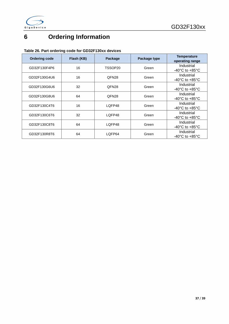
6 Ordering Information
Table 26. Part ordering code for GD32F130xx devices
Ordering code Flash (KB) Package Package type Temperature operating range
GD32F130F4P6 16 TSSOP20 Green Industrial -40°C to +85°C
GD32F130G4U6 16 QFN28 Green Industrial -40°C to +85°C
GD32F130G6U6 32 QFN28 Green Industrial -40°C to +85°C
GD32F130G8U6 64 QFN28 Green Industrial -40°C to +85°C
GD32F130C4T6 16 LQFP48 Green Industrial -40°C to +85°C
GD32F130C6T6 32 LQFP48 Green Industrial -40°C to +85°C
GD32F130C8T6 64 LQFP48 Green Industrial -40°C to +85°C
GD32F130R8T6 64 LQFP64 Green Industrial -40°C to +85°C
GD32F130xx
38 / 39
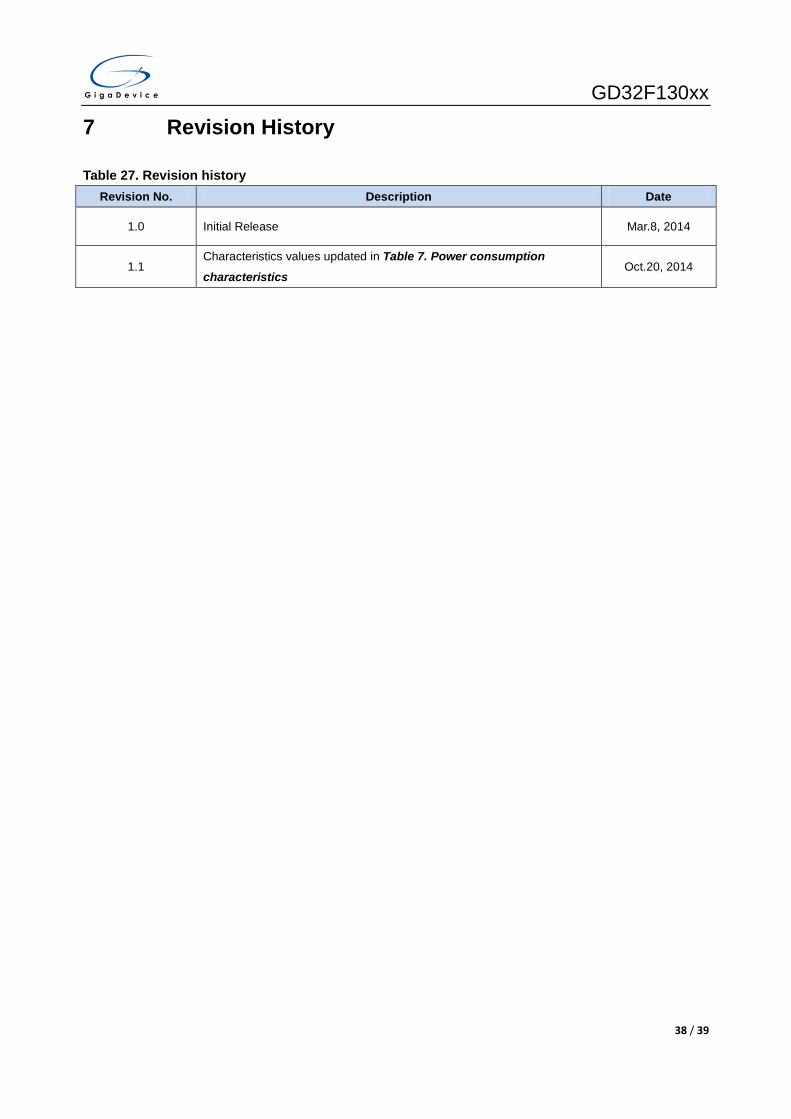
7 Revision History
Table 27. Revision history Revision No. Description Date
1.0 Initial Release Mar.8, 2014
1.1 Characteristics values updated in Table 7. Power consumption
characteristics Oct.20, 2014