gergely ferenc samu -...
TRANSCRIPT
Ph. D. Dissertation
Characterization of optically active
perovskite electrodes
Gergely Ferenc Samu
Supervisors:
Dr. Csaba Janáky
Assistant professor
Prof. Csaba Visy
Professor emeritus
DOCTORAL SCHOOL OF CHEMISTRY
University of Szeged
Faculty of Science and Informatics
Department of Physical Chemistry and Materials Science
Szeged
2018
Ph. D. Dissertation Table of Contents
I
Table of contents
1. Introduction .............................................................................................................................. 1
1.1. Properties of Perovskites ................................................................................................. 2
1.1.1. Structural Considerations ....................................................................................... 2
1.1.2. Synthetic Strategies to Prepare Perovskites........................................................... 5
1.1.3. Optoelectronic Properties ........................................................................................ 8
1.1.4. Instability of Perovskites ....................................................................................... 14
1.1.5. Light-Induced Phase Segregation in Mixed Halide Perovskites ........................ 20
1.1.6. Electrochemical Properties of Perovskites ........................................................... 20
1.2. Perovskite Solar Cells .................................................................................................... 24
1.2.1. General Solar Cell Architectures .......................................................................... 25
1.2.2. Hole Transport Layer ............................................................................................ 28
1.3. Conducting Polymers as Hole Transporters in Perovskite Solar Cells ..................... 29
2. Aims ......................................................................................................................................... 31
3. Materials and Methods .......................................................................................................... 32
3.1. Materials ......................................................................................................................... 32
3.2. Synthesis .......................................................................................................................... 33
3.2.1. Synthesis of CsPbBr3 Nanocrystals ....................................................................... 33
3.2.2. Synthesis of CH3NH3PbBrxI3-x ............................................................................... 33
3.2.3. Synthesis of Bis-EDOT ........................................................................................... 34
3.3. Methods ........................................................................................................................... 34
3.3.1. Electrode/Solar Cell Preparation .......................................................................... 34
3.3.2. Spin-coating Protocols ........................................................................................... 35
3.3.3. Preparation of CH3NH3PbI3 Solar Cells .............................................................. 36
3.3.4. Inducing Phase Segregation .................................................................................. 36
3.3.5. Electrodeposition of PEDOT ................................................................................. 36
3.4. Physical Characterization .............................................................................................. 37
3.4.1. Electrochemistry/Spectroelectrochemistry .......................................................... 37
3.4.2. Ultrafast Transient Spectroelectrochemistry....................................................... 39
3.4.3. X-ray Photoelectron Spectroscopy ........................................................................ 42
3.4.4. Scanning Electron Microscopy.............................................................................. 42
3.4.5. X-ray Diffraction .................................................................................................... 42
3.4.6. Raman-spectroscopy .............................................................................................. 42
3.4.7. Solar Cell Characterization ................................................................................... 43
4. Results and Discussion ........................................................................................................... 45
4.1. Establishing the Electrochemical Stability Window of Perovskite Electrodes ......... 45
Ph. D. Dissertation Table of Contents
II
4.1.1. UV-vis Spectroscopic Studies of the Dissolution of CsPbBr3 Electrodes........... 45
4.1.2. Spectroelectrochemistry of CsPbBr3 Electrodes ................................................. 46
4.1.3. Chemical Composition of Reduced/Oxidized CsPbBr3 Electrode Surfaces ...... 48
4.1.4. Structural Changes of Reduced/Oxidized CsPbBr3 Electrodes ......................... 51
4.1.5. Morphological Changes of Reduced/Oxidized CsPbBr3 Electrodes .................. 54
4.1.6. Spectroelectrochemistry of PbBr2 Electrodes ...................................................... 55
4.1.7. UV-vis Spectroscopic Studies of the Dissolution of CH3NH3PbI3 Electrodes ... 56
4.1.8. Spectroelectrochemistry of CH3NH3PbI3 Electrodes .......................................... 58
4.1.9. Spectroelectrochemistry of PbI2 Electrodes ......................................................... 59
4.1.10. Potential Diagram of Optically Active Perovskite Electrodes ............................ 60
4.1.11. Best Practice for Electrochemical Experiments .................................................. 61
4.2. Ultrafast Transient Spectroelectrochemistry of Perovskite Photoelectrodes ........... 63
4.2.1. Transient Absorption of CsPbBr3 with Applied Bias ......................................... 63
4.2.2. Effect of Electrochemical Bias on the Charge Carrier Recombination ............ 65
4.2.3. Reversibility of Bleaching Recovery Kinetics to Applied Bias ........................... 66
4.2.4. The Influence of TiO2 Layer on Bleaching Recovery Lifetime .......................... 69
4.3. Light-Induced Phase Segregation in Mixed Halide Perovskite Solar Cells .............. 71
4.3.1. UV-vis Spectroscopic Monitoring of Phase Segregation in CH3NH3PbBr1.5I1.5
Solar Cells ............................................................................................................................... 71
4.3.2. Effect of Phase Segregation on the Efficiency of CH3NH3PbBr1.5I1.5 Solar Cells .
.................................................................................................................................. 72
4.3.3. Effect of Phase Segregation on the Quantum Efficiency of Solar Cells ............ 72
4.4. Electrosynthesis of PEDOT Hole Transporter Layer on CH3NH3PbI3 Electrodes .. 76
4.4.1. Spectroelectrochemistry of PEDOT Deposition on CH3NH3PbI3 Electrodes ... 76
4.4.2. Morphological Features of Electrodeposited PEDOT ........................................ 78
4.4.3. Efficiency of Solar Cells Employing Electrodeposited PEDOT Hole
Transporter ............................................................................................................................. 79
4.4.4. Electrochemical Post Treatment of the Deposited PEDOT Hole Transporter . 80
4.4.5. Fine-tuning the Electrochemical Post Treatment ................................................ 83
4.4.6. Transient Absorption Spectroscopy of Electrodeposited PEDOT Hole
Transporters ........................................................................................................................... 85
5. Summary ................................................................................................................................. 88
6. Összefoglalás ........................................................................................................................... 91
7. References ............................................................................................................................... 94
Acknowledgements ....................................................................................................................... 104
Ph. D. Dissertation List of Figures
III
List of Figures
Figure 1. The improvement in power conversion efficiency of perovskite solar cells over the
years, graphed together with the number of publications and the number of generated
citations (Web of Knowledge statistics 2018.01.01 search term: perovskite solar cell). ...... 1
Figure 2. Crystal structure of a 3D HOIP, with a general stoichiometry of ABX3. ............. 3
Figure 3. Formation landscape of 3D lead (red line) and tin (blue line) perovskites as a
function of A-site cation and X-site anion size. Solid and dashed lines mark the bounds of
tolerance and octahedral factors respectively. Adapted from ref. [19] .................................. 4
Figure 4. HOIP thin film deposition methods. A: Antisolvent assisted spin-coating method.
B: Two-step (sequential) deposition spin-coating method. C: Vapor deposition (co-
evaporation) method. Adopted from ref.[26] ........................................................................... 6
Figure 5. Summary of optoelectronic properties of HOIPs. ................................................. 9
Figure 6. A: UV-vis absorption spectra of MAPbBrxI3−x thin layers. The inset shows the
determined optical bandgap from the onset of the absorption spectra. B: Representation of
the electronic band diagram of MAPbBrxI3−x compounds. ................................................. 11
Figure 7. Schematic representation of the various photophysical processes in perovskites
following photoexcitation. Adapted from ref.[90]. ................................................................ 13
Figure 8. Important factors governing the stability HOIPs. ............................................... 14
Figure 9. Illustration of the different migration pathways in a MAPbI3 lattice. A: The
migration of I−, Pb2+, and MA+ ions through vacancies. B: Different migration pathways
considering bulk-point defects, lattice distortions, and grain boundaries. Adapted from ref. [134]. ...................................................................................................................................... 19
Figure 10. The evolution of PSC architectures. Adapted from ref.[176]. ............................. 25
Figure 11. Skeletal structural formula of commonly employed organic hole transporter
materials. ............................................................................................................................. 28
Figure 12. Schematic representation of the different architectures used throughout the
experiments. A: Complete solar cell, B: partially complete solar cell and C: electrode. .. 34
Figure 13. A: Photograph of a fully assembled MAPbI3 solar cell. B: The evolution of
MAPbI3 solar cell efficiencies throughout the course of the work. ..................................... 36
Figure 14. Schematic representation of the spectroelectrochemical setup, together with the
photograph of the cell. ......................................................................................................... 37
Figure 15. The used measurement setup for the ultrafast transient spectroelectrochemistry
measurements. ..................................................................................................................... 39
Figure 16. A: Energy levels of a hypothetical optically active sample and some quantum
transitions influencing the difference absorption spectrum. B: The corresponding difference
absorption spectrum with the separate contributions of the different transitions. .............. 41
Figure 17. A: Typical j-V response of a MAPbI3 solar cell under dark, reverse and forward
sweep conditions. The sweep rate was 50 mV s−1 and the used illumination was 1.5 AM 100
mW cm−2. B: The equivalent circuit model of a realistic solar cell. ................................... 43
Ph. D. Dissertation List of Figures
IV
Figure 18. UV-vis absorbance spectra of FTO/TiO2/CsPbBr3 films in different electrolytes,
after different immersion times. A: pure DCM, B: 0.1 M Bu4NBF4 in DCM, C: 0.1 M
Bu4NClO4 in DCM, D: 0.1 M Bu4NPF6 in DCM. ............................................................... 45
Figure 19. Normalized absorbance change at 518 nm of FTO/TiO2/CsPbBr3 electrodes in
different DCM based electrolytes. The error bars were derived from measurements on three
separate films. ...................................................................................................................... 46
Figure 20. Spectroelectrochemical data, recorded for FTO/TiO2/CsPbBr3 films in 0.1 M
Bu4NPF6/DCM electrolyte (10 mV s−1 sweep rate). A: Three subsequent CV curves recorded
during oxidation B: UV-vis spectra recorded at various potentials during oxidation. C: The
first oxidation half cycle plotted together, with the absorbance change at the excitonic peak.
............................................................................................................................................. 47
Figure 21. A: UV-vis absorbance spectrum of a FTO/TiO2/CsPbBr3 film in 0.1 M Bu4NPF6.
Difference spectra after B: different immersion times and C: oxidation treatment. ........... 47
Figure 22. Spectroelectrochemical data, recorded for FTO/TiO2/CsPbBr3 films in 0.1 M
Bu4NPF6/DCM electrolyte (10 mV s−1 sweep rate). A: Three subsequent CV curves recorded
during reduction B: UV-vis spectra recorded at various potentials during reduction. C: The
reduction half cycle plotted together, with the absorbance change at excitonic peak. ....... 48
Figure 23. Photographs of FTO/TiO2/CsPbBr3 electrodes treated at selected potential
values for 30 s. ..................................................................................................................... 48
Figure 24. High resolution XPS data for the FTO/TiO2/CsPbBr3 electrodes treated at
selected potential values (as-is, −1.4 V, +0.8 V, +1.5 V), for 30 s in 0.1 M Bu4NPF6/DCM
solution. A: Cs 3d, B: Pb 4f, C: Br 3d, D: F 1s, E: O 1s XP spectrum. ............................. 49
Figure 25. A: XRD patterns for the FTO/TiO2/CsPbBr3 electrodes treated at selected
potential values (as is, −1.4 V, +0.8 V, +1.5 V) for 30 s in 0.1 M Bu4NPF6/DCM solution.
The peaks marked with # represent overlapping diffractions of CsPbBr3 and the FTO/TiO2
substrate. B: Magnified regions of the diffraction patterns of the samples held at −1.4 V and
+0.8 V. The peaks marked with * belong to the untreated FTO/TiO2/CsPbBr3 electrodes. 51
Figure 26. High resolution XPS data for the FTO/TiO2/CsPbBr3 electrodes, treated at
selected potential values (OCP, −0.4 V, and +0.4 V) for 30 s in 0.1 M Bu4NPF6/DCM
solution. A: Cs 3d, B: Pb 4f, C: Br 3d, D: F 1s, E: O 1s XP spectrum. ............................. 53
Figure 27. SEM images for the FTO/TiO2/CsPbBr3 electrodes treated at selected potential
values (A: OCP, B: +0.4 V, and C: −0.4 V) for 30 s in 0.1 M Bu4NPF6/DCM solution. ... 54
Figure 28. SEM images of CsPbBr3 films both from top and side views. A, E: pristine, B, F:
reduced at E = −1.4 V, C, G: oxidized at E = +0.8 V, D, H: oxidized at E = +1.4 V. All
treatments lasted 30 s in 0.1 M Bu4NPF6/DCM solution. ................................................... 55
Figure 29. SEM image and EDX data recorded for a FTO/TiO2/CsPbBr3 electrode treated
at E = ‒1.4 V for 30 s in 0.1 M Bu4NPF6/DCM solution. ................................................... 55
Figure 30. Three subsequent CV curves recorded in 0.1 Bu4NPF6/DCM solution (10 mV s−1
sweep rate), during the A: oxidation and B: reduction of the PbBr2 films deposited on
FTO/TiO2 electrodes. UV-vis spectra recorded during C: oxidation and D: reduction
processes. ............................................................................................................................. 56
Ph. D. Dissertation List of Figures
V
Figure 31. UV-vis absorbance spectra of FTO/TiO2/MAPbI3 films in different electrolytes,
after different immersion times. A: pure DCM, B: 0.1 M Bu4NBF4 in DCM, C: 0.1 M
Bu4NClO4 in DCM, D: 0.1 M Bu4NPF6 in DCM, E: 0.01 M Bu4NPF6 in DCM. ................ 57
Figure 32. Kinetic curves of the normalized absorbance change at 470 nm, recorded for
FTO/TiO2/MAPbI3 in different DCM based electrolytes. The error bars were derived from
the measurement of three separate films. ............................................................................ 58
Figure 33. Spectroelectrochemical data, recorded for FTO/TiO2/MAPbI3 films in 0.1 M
Bu4NPF6/DCM solution (10 mV s−1 sweep rate), during the first A: oxidation and B:
reduction half cycles together with the absorbance changes at 470 nm. ............................ 58
Figure 34. Three subsequent CV curves recorded during the A: oxidation and B: reduction
of FTO/TiO2/MAPbI3 electrodes in 0.01 Bu4NPF6/DCM solution (10 mV s−1 sweep rate).
UV-vis spectra recorded during the first C: oxidation and D: reduction half-cycle. ......... 59
Figure 35. Three subsequent CV curves recorded in 0.1 Bu4NPF6/DCM solution (10 mV s−1
sweep rate), during the A: oxidation and B: reduction of the PbI2 films deposited on
FTO/TiO2 electrodes. UV-vis spectra recorded during the first C: oxidation and D:
reduction half-cycles............................................................................................................ 60
Figure 36. Comparison of the band edge positions and the potential of various redox events
detected for the studied two lead halide perovskites. .......................................................... 61
Figure 37. A: Time vs. applied potential curve recorded during electrochemical stability
measurements. The potential was ramped from −0.6 V to +0.6 V and then back to −0.6 V.
B: Time vs. the normalized absorbance at 518 nm (excitonic peak) of the FTO/TiO2/CsPbBr3
film used for the electrochemical stability test. C: Absorbance spectra of the
FTO/TiO2/CsPbBr3 film before and after the cycling of applied bias. ................................ 63
Figure 38. Difference absorption spectra of an FTO/TiO2/CsPbBr3 film measured A: in
vacuum (without electrolyte) and B: in DCM containing 0.1 M Bu4NPF6 electrolyte (with
electrolyte) under OCP conditions (no external bias was used). C: Respective bleaching
recovery profiles recorded in the two different media. ....................................................... 64
Figure 39. Time resolved transient spectra recorded following 387 nm laser pulse excitation
(4J cm−2) of FTO/TiO2/CsPbBr3 electrode in a spectroelectrochemical cell with deaerated
DCM containing 0.1 M Bu4NPF6 electrolyte. The spectra were recorded at applied
potentials of A: +0.4V; B: −0.4 V; C: +1.0 V and D: −1.2 V vs. Ag/AgCl. ....................... 65
Figure 40. A: Bleaching recovery profiles, B: kinetic fit 1/A vs. time and C: relative pseudo
first order rate constants determined from the slope of plots in B with the dashed line to
guide the eye (The magnitude of bleaching was kept constant at A = −0.25 for all these
experiments so that initial charge carrier concentration is same in all experiments). The
applied potentials range was between −0.6 and +0.6 V vs. Ag/AgCl. ................................ 66
Figure 41. Dependence of bleaching recovery lifetime determined from the inverse slope of
the kinetic fit of 1/A vs. time. Measurements were carried out with FTO/TiO2/CsPbBr3
electrodes in deaerated DCM containing 0.1 M Bu4NPF6 electrolyte. The electrodes were
biased at set potentials in the range −0.6 V to +0.5 V vs. Ag/AgCl and excited with 387 nm
laser pulse to record time resolved TA spectra. .................................................................. 67
Ph. D. Dissertation List of Figures
VI
Figure 42. Difference absorption spectra of an FTO/TiO2/CsPbBr3 film at different applied
potentials on a forward and reverse scan. Spectra are shown for A: −0.4 V forward; B: 0.0
V forward; C: +0.4 V forward; D: −0.4 V reverse; E: 0.0 V reverse; F: +0.4 V reverse. The
same film was used for all measurements seen here. However, the film was moved to different
positions so that degradation due to the pump laser pulse would not occur. ..................... 68
Figure 43. Dependence of bleaching recovery lifetime determined from the inverse slope of
the kinetic fit of 1/A vs. time. Measurements were carried out with FTO/CsPbBr3 electrodes
in deaerated DCM containing 0.1 M Bu4NPF6 electrolyte. The electrodes were biased at set
potentials in the range −0.4 V to +0.5 V vs. Ag/AgCl and excited with 387 nm laser pulse to
record time resolved TA spectra. ......................................................................................... 69
Figure 44. Schematic diagram illustrating the band energies and the Fermi level response
to applied bias. The charge transfer from excited perovskite to TiO2 (kET) competes with the
charge recombination (kr) is influenced by the electron accumulation (or depletion) during
electrochemical bias ............................................................................................................ 70
Figure 45. A: Absorption spectra of mixed halide perovskite film (a) before and (b) after
irradiation for 30 minutes. Spectrum (c) shows dark recovery after three hours. B:
Difference absorption spectra after 30 min light soaking shows dark recovery. ................ 71
Figure 46. A: j-V curves of the champion cell (a) in dark, (b) before light soaking, and (c)
after light soaking for 30 minutes. B: Effect of 15 minute and 30 minute light soaking on the
performance of four MAPBBr1.5I1.5 perovskite based cells. The measured photoconversion
efficiency before and after light soaking presented in the figure show the effect of light
soaking on the photovoltaic performance. .......................................................................... 72
Figure 47. A: IPCE of mixed halide PSC (a) before light soaking and (b) – (f) during dark
recovery following 30 min light soaking. A 420 nm cut-off filter was used for IPCE
measurements and residual dark currents were corrected for IPCE measurements. B:
Difference IPCE spectra showing the recovery of the solar cell response in the 500-700 nm
region. (The spectra were normalized at 470 nm and the IPCE recorded before the
continuous irradiation was used as the reference.) ............................................................. 73
Figure 48. Recovery traces recorded after light soaking of MAPbBr1.5I1.5 based solar cells
for 30 minutes (a) the recovery of the bleaching (observed at 620 nm) using a partially
assembled cell and (b) the overall IPCE recovery of a complete cell. ................................ 73
Figure 49. Difference IPCE recorded for MAPbI3 based solar cell irradiated for 30 minutes
(the IPCE data were normalized at 450 nm). ...................................................................... 74
Figure 50. Schematic representation of phase segregation in mixed-halide (MAPbBr1.5I1.5)
solar cells, and its effect on the charge collection of such devices. .................................... 75
Figure 51. A: Potentiodynamic deposition of PEDOT with 25 mV s−1 sweep rate in a 0.01
M bis-EDOT, 0.1 M Bu4NPF6 DCM solution on a solar cell architecture (FTO/bl-TiO2/mp-
TiO2/MAPbI3) employing a thin MAPbI3 layer. B: UV-vis absorbance spectra recorded after
each cycle at E = 0.0 V during polymerization. C: First half-cycle of the potentiodynamic
deposition plotted together with the absorbance change at 700 nm. .................................. 77
Figure 52. A: Potentiostatic deposition of PEDOT at different potentials in a 0.01 M bis-
EDOT, 0.1 M Bu4NPF6 DCM solution on a solar cell architecture employing regular
Ph. D. Dissertation List of Figures
VII
thickness MAPbI3 layers with a polymerization charge density of 10 mC cm−2. B: UV-vis
absorbance spectra of solar cells after PEDOT electrodeposition at E = +0.9 V for different
polymerization charge densities. C: The absorbance change of the solar cells compared to
a HTM-free cell by varying the polymerization charge density at different applied potentials.
............................................................................................................................................. 77
Figure 53. A: Top-view SEM image before (upper part) and after PEDOT (lower part)
electrodeposition. B: Cross sectional FIB-SEM image of a solar cell, where the PEDOT
electrodeposition was carried out at E = +1.0 V with Qpol = 5 mC cm−2. C: Theoretical and
actual PEDOT layer thicknesses (determined from cross-sectional SEM images). D: Raman-
spectra of a fully assembled solar cell architecture and a FTO/PEDOT reference. .......... 78
Figure 54. The effect of PEDOT thickness (polymerization charge density) in a
FTO/TiO2/MAPbI3/PEDOT solar cell on the A: short circuit current density, B: open circuit
voltage, C: fill factor, and D: overall efficiency. The solar cells were tested under 1 sun (100
mW cm−2) illumination, with a 50 mV s−1 sweep rate. ........................................................ 79
Figure 55. The effect of PEDOT thickness (polymerization charge density) in a
FTO/TiO2/MAPbI3/PEDOT solar cell for PEDOT layers electrodeposited at E = +1.0 V. A:
on the open circuit voltage B: on the j-V profile of the solar cell in the dark (50 mV s−1). 80
Figure 56. Schematic representation of PEDOT doping. ................................................... 81
Figure 57. Chronoamperometric curves recorded for the post-treatment of a
FTO/TiO2/MAPbI3/PEDOT solar cell, where the PEDOT layers were electrodeposited at E
= +1.0 V, A: when an oxidative post-treatment at E = +0.6 V and B: when a reductive post-
treatment at E = −0.6 V was employed. .............................................................................. 81
Figure 58. Development of the open circuit voltage in a FTO/TiO2/MAPbI3/PEDOT solar
cell for the PEDOT layers electrodeposited at E = +1.0 V for Qpol = 10 mC cm−2 as a
function of redox treatment. ................................................................................................ 82
Figure 59. Cross-sectional SEM images of a solar cell, where the PEDOT electrodeposition
was carried out at E = +1.0 V for A: Qpol = 5 mC cm−2, and B: Qpol = 10 mC cm−2. In both
cases the electrodeposition was immediately followed by a reduction step at E = −0.6 V for
t = 60 s. ................................................................................................................................ 83
Figure 60. Chronoamperometric curves recorded for the post-treatment of
FTO/TiO2/MAPbI3/PEDOT solar cells, where the PEDOT layers were electrodeposited at
E = +1.0 V. A reductive post treatment of A: rapid reduction at E = −0.6 V for t = 10 s, B:
mild reduction at E = −0.5 V for t = 60 s, and C: rapid-mild reduction at E = −0.5 V for t
= 20 s was used. .................................................................................................................. 84
Figure 61. The effect of PEDOT thickness (polymerization charge density) on the open
circuit voltage in a FTO/TiO2/MAPbI3/PEDOT solar cell for PEDOT layers
electrodeposited at E = +1.0 V. The applied post-reduction step was A: rapid reduction at
E = −0.6 V for t = 10 s, B: mild reduction at E = −0.5 V for t = 60 s, and C: rapid-mild
reduction at E = −0.5 V for t = 20 s. .................................................................................. 84
Figure 62. J-V curve of the champion device containing a PEDOT layer electrodeposited at
E = +1.0 V for Qpol = 10 mC cm−2, where the post-reduction step was at E = −0.6 V for t =
10 s. ...................................................................................................................................... 85

Ph. D. Dissertation List of Figures
VIII
Figure 63. A: Time-resolved transient spectra of an FTO/TiO2/MAPbI3/PEDOT solar cell
employing a thin MAPbI3 layer following 387 nm laser pulse excitation. The PEDOT layer
was prepared and post-treated just as the champion device. B: Bleaching recovery profiles
at 760 nm of different FTO/TiO2/MAPbI3/PEDOT solar cells. ........................................... 86
Ph. D. Dissertation List of Tables
IX
List of Tables
Table 1. Summary of the performance of the HOIPs used in Li-intercalation studies. In
brackets the charging current density is shown. ................................................................. 23
Table 2. Drying conditions of the different conducting electrolytes. .................................. 38
Table 3. Compositional analysis of the surface of the electrochemically treated
FTO/TiO2/CsPbBr3 electrodes using XPS. The standard deviation values were derived from
analyzing XP spectra captured from three different spots of the sample. ........................... 50
Table 4. Compositional analysis of the surface of the FTO/TiO2/CsPbBr3 electrodes oxidized
at selected potential values using XPS. ............................................................................... 51
Table 5. Compositional analysis of the surface of the mildly treated FTO/TiO2/CsPbBr3
electrodes using XPS. .......................................................................................................... 53
Table 6. Parameters to conduct (spectro)electrochemical experiments. ............................ 62
Table 7. Determined lifetimes, from biexponential fits carried out on TA data. The standard
deviation of the measurements was calculated from three separate measurements. .......... 86
Ph. D. Dissertation List of Abbreviations
X
List of Abbreviations
CB – Conduction band
CV – Cyclic voltammetry
DSSC – Dye-sensitized solar cell
ECL – Electrochemiluminescence
EDX – Energy dispersive X-ray spectroscopy
ETL – Electron transport layer
FIB – Focused ion beam
HOIP – Hybrid organic-inorganic perovskite
HTL / HTM – Hole transport layer / Hole transport material
IPCE – Incident photon to charge carrier conversion efficiency
JSC – Short-circuit current density
VOC – Open circuit potential
PSC – Perovskite solar cell
SEM – Scanning electron microscopy
TAS – Transient absorption spectroscopy
UV-vis – Ultraviolet-visible
VB – Valence band
VOC – Open-circuit voltage
XPS – X-ray photoelectron spectroscopy
XRD – X-ray diffraction
Chemicals
DCM – Dichloromethane
DMF – N,N-dimethylformamide
DMSO – Dimethylsulfoxide
FTO – Fluorine doped tin oxide
GBL – -butyrolactone
MAPbX3 – CH3NH3PbX3
MAI – Methylammonium-iodide
PEDOT – Poly(3,4-ethylenedioxythiophene)
spiro-MeOTAD – 2,2′,7,7′-tetrakis(N,N′-di-p-methoxyphenylamine)-9,9′-spirobifluorene
Ph. D. Dissertation 1. Introduction
1
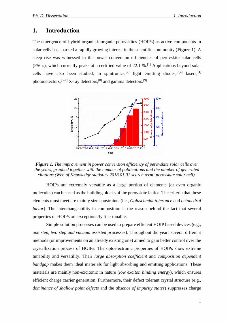
1. Introduction
The emergence of hybrid organic-inorganic perovskites (HOIPs) as active components in
solar cells has sparked a rapidly growing interest in the scientific community (Figure 1). A
steep rise was witnessed in the power conversion efficiencies of perovskite solar cells
(PSCs), which currently peaks at a certified value of 22.1 %.[1] Applications beyond solar
cells have also been studied, in spintronics,[2] light emitting diodes,[3,4] lasers,[4]
photodetectors,[5–7] X-ray detectors,[8] and gamma detectors.[9]
Figure 1. The improvement in power conversion efficiency of perovskite solar cells over
the years, graphed together with the number of publications and the number of generated
citations (Web of Knowledge statistics 2018.01.01 search term: perovskite solar cell).
HOIPs are extremely versatile as a large portion of elements (or even organic
molecules) can be used as the building blocks of the perovskite lattice. The criteria that these
elements must meet are mainly size constraints (i.e., Goldschmidt tolerance and octahedral
factor). The interchangeability in composition is the reason behind the fact that several
properties of HOIPs are exceptionally fine-tunable.
Simple solution processes can be used to prepare efficient HOIP based devices (e.g.,
one-step, two-step and vacuum assisted processes). Throughout the years several different
methods (or improvements on an already existing one) aimed to gain better control over the
crystallization process of HOIPs. The optoelectronic properties of HOIPs show extreme
tunability and versatility. Their large absorption coefficient and composition dependent
bandgap makes them ideal materials for light absorbing and emitting applications. These
materials are mainly non-excitonic in nature (low exciton binding energy), which ensures
efficient charge carrier generation. Furthermore, their defect tolerant crystal structure (e.g.,
dominance of shallow point defects and the absence of impurity states) suppresses charge
Ph. D. Dissertation 1. Introduction
2
carrier recombination processes and their ambipolar charge transport improves charge
carrier extraction. These qualities are the underlying reasons for the remarkable efficiency
of the derived solar cells.
Currently the limiting factor of the commercialization of HOIP based devices is their
sensitivity towards several environmental factors (e.g., humidity, heat, light). Furthermore,
device architecture, operational conditions (such as built-in electric fields) and other
components of the devices (interfacial layers, electrode corrosion) can also detrimentally
affect device performance.
Electrochemistry as a characterization tool, has started to gain a foothold in the
evaluation of HOIP materials. Currently the field is in its infancy, however the first studies
are already available of HOIP based electrodes in different electrochemical applications
(e.g., Li-ion batteries, electrochemiluminescence). Electrochemical techniques can offer
valuable information about the charge carrier generation and transport in HOIPs. With the
aid of coupled techniques the chemical changes upon charge carrier generation can also be
unraveled. Fundamental optoelectronic properties can also be studied (e.g., band edge
positions, distribution of trap states). In addition, electrochemical methods can be also used
as synthetic tools. The use of HOIP photoelectrodes to drive certain reduction reactions (e.g.,
CO2 reduction) is an especially lucrative concept. Furthermore, electrochemistry can also
aid the assembly of HOIP based devices. All these opportunities call for coherent stability
tests, so the degradation of the HOIP based electrodes could be avoided.
1.1. Properties of Perovskites
1.1.1. Structural Considerations
Perovskites constitute an intriguing class of materials, which have played a pivotal
role in the evolution of materials chemistry and condensed matter physics. The
crystallographic family itself bears the name of the Russian mineralogist Lev A. Perovski.
However, the first perovskite compound (CaTiO3), was discovered by Gustav Rose in 1839.
These materials adopt a general stoichiometry of ABX3. Initially oxide compounds
dominated this crystallographic family. In recent years the adaptability of the perovskite
structure to site substitution gave rise to a new class of perovskites, namely HOIPs.
Normally, the A site can be occupied by a monovalent organic cation (e.g.,
methylammonium (CH3NH3+, MA+), formamidinium (CH(NH2)2
+, FA) or inorganic cation
(e.g., K+, Rb+, Cs+). The B site is a divalent metal cation (e.g., Pb2+, Sn2+, Ge2+) and the X
Ph. D. Dissertation 1. Introduction
3
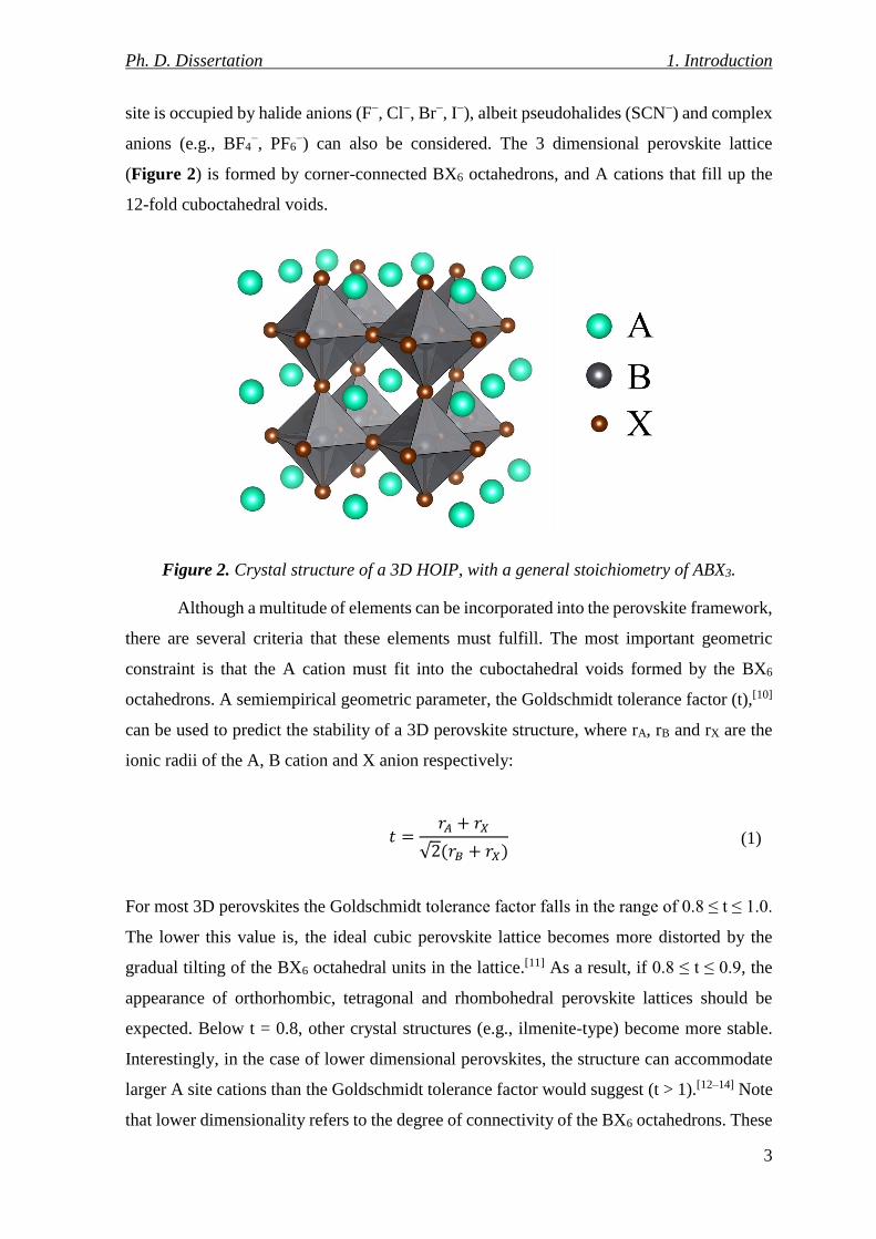
site is occupied by halide anions (F−, Cl−, Br−, I−), albeit pseudohalides (SCN−) and complex
anions (e.g., BF4−, PF6
−) can also be considered. The 3 dimensional perovskite lattice
(Figure 2) is formed by corner-connected BX6 octahedrons, and A cations that fill up the
12-fold cuboctahedral voids.
Figure 2. Crystal structure of a 3D HOIP, with a general stoichiometry of ABX3.
Although a multitude of elements can be incorporated into the perovskite framework,
there are several criteria that these elements must fulfill. The most important geometric
constraint is that the A cation must fit into the cuboctahedral voids formed by the BX6
octahedrons. A semiempirical geometric parameter, the Goldschmidt tolerance factor (t),[10]
can be used to predict the stability of a 3D perovskite structure, where rA, rB and rX are the
ionic radii of the A, B cation and X anion respectively:
𝑡 =𝑟𝐴 + 𝑟𝑋
√2(𝑟𝐵 + 𝑟𝑋) (1)
For most 3D perovskites the Goldschmidt tolerance factor falls in the range of 0.8 ≤ t ≤ 1.0.
The lower this value is, the ideal cubic perovskite lattice becomes more distorted by the
gradual tilting of the BX6 octahedral units in the lattice.[11] As a result, if 0.8 ≤ t ≤ 0.9, the
appearance of orthorhombic, tetragonal and rhombohedral perovskite lattices should be
expected. Below t = 0.8, other crystal structures (e.g., ilmenite-type) become more stable.
Interestingly, in the case of lower dimensional perovskites, the structure can accommodate
larger A site cations than the Goldschmidt tolerance factor would suggest (t > 1).[12–14] Note
that lower dimensionality refers to the degree of connectivity of the BX6 octahedrons. These
Ph. D. Dissertation 1. Introduction
4
lower dimensional perovskites, are specific cuts or slices of the parent 3D perovskite
structure.
The Goldschmidt tolerance factor is an often-used tool to predict possible material
compositions that could form a perovskite lattice. It has been shown that it is a necessary but
not sufficient condition as other space filling restrictions should also be considered.[15,16] One
such is the stability of the BX6 octahedron, which can be described by the octahedral factor
():
𝜇 =𝑟𝐵𝑟𝑋
(2)
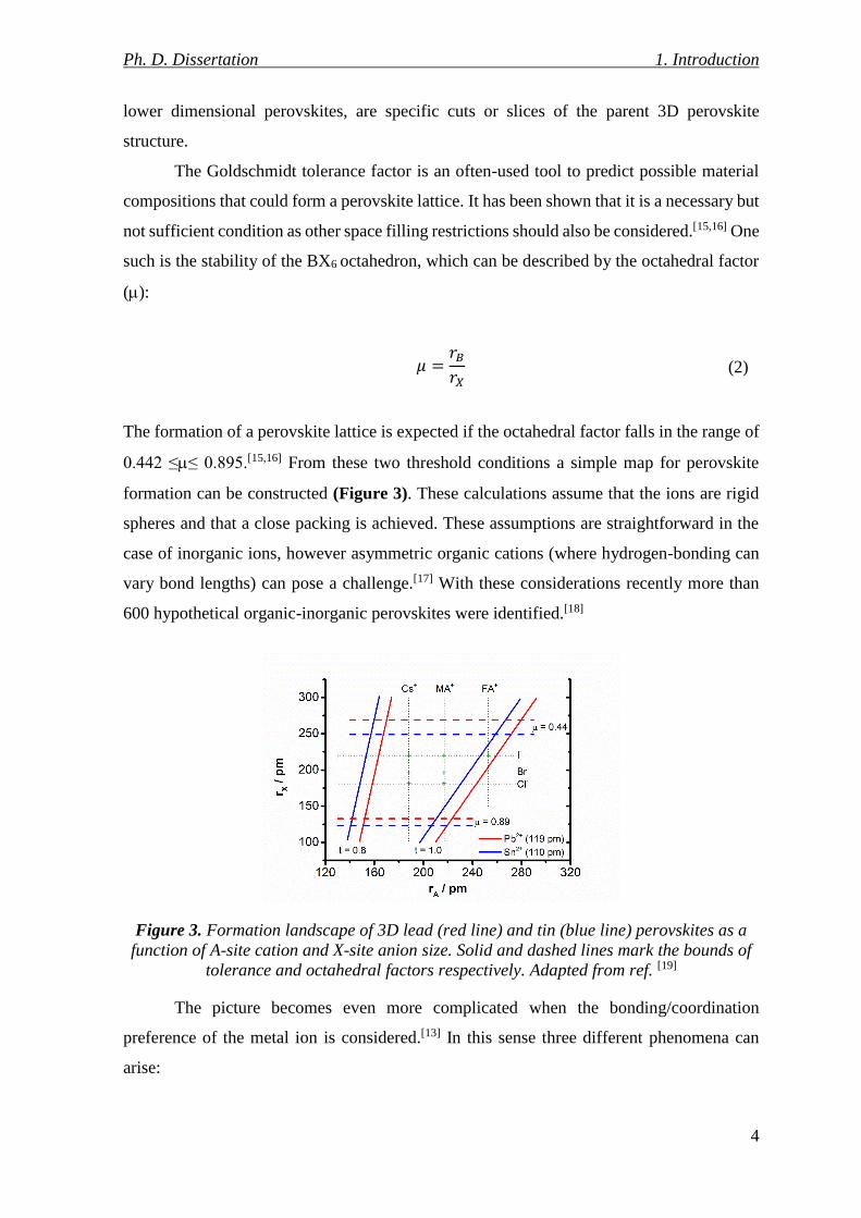
The formation of a perovskite lattice is expected if the octahedral factor falls in the range of
0.442 ≤≤ 0.895.[15,16] From these two threshold conditions a simple map for perovskite
formation can be constructed (Figure 3). These calculations assume that the ions are rigid
spheres and that a close packing is achieved. These assumptions are straightforward in the
case of inorganic ions, however asymmetric organic cations (where hydrogen-bonding can
vary bond lengths) can pose a challenge.[17] With these considerations recently more than
600 hypothetical organic-inorganic perovskites were identified.[18]
Figure 3. Formation landscape of 3D lead (red line) and tin (blue line) perovskites as a
function of A-site cation and X-site anion size. Solid and dashed lines mark the bounds of
tolerance and octahedral factors respectively. Adapted from ref. [19]
The picture becomes even more complicated when the bonding/coordination
preference of the metal ion is considered.[13] In this sense three different phenomena can
arise:
Ph. D. Dissertation 1. Introduction
5
The lone s2 electron pair of the B site metal ion is stereochemically active, it can shift
the metal ion away from the crystallographic center of the BX6 octahedron, thus
causing a distortion in the perovskite framework.[20] This effect is particularly
dominant in the case of Ge2+ based perovskites and becomes less prominent in the
case of Pb2+.[21,22]
In HOIPs the organic cation occupying the A site can also cause the distortion of the
perovskite framework, through directional hydrogen bonding to the halide cage.[22]
Jahn-Teller and related distortions can also affect the stability of the perovskite
lattice.[23]
Apart from ionic radii constraints an overall neutral charge must also be achieved. If
the A site cation is monovalent and the X site is occupied by a halogen, then the B site metal
must be divalent. However, there are exceptions to this rule, as equal number of +1 and +3
metal cations can yield an overall +2 charge. In this notion the formation of more complex
mixed-valent perovskites (e.g., Cs2Au(I)Au(III)I6) is also feasible, which further enriches
the already broad family of perovskites.[24,25]
1.1.2. Synthetic Strategies to Prepare Perovskites
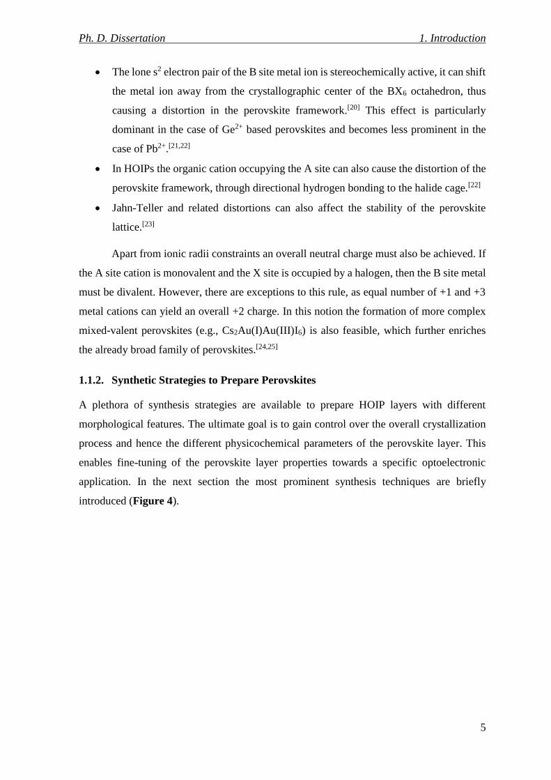
A plethora of synthesis strategies are available to prepare HOIP layers with different
morphological features. The ultimate goal is to gain control over the overall crystallization
process and hence the different physicochemical parameters of the perovskite layer. This
enables fine-tuning of the perovskite layer properties towards a specific optoelectronic
application. In the next section the most prominent synthesis techniques are briefly
introduced (Figure 4).
Ph. D. Dissertation 1. Introduction
6
Figure 4. HOIP thin film deposition methods. A: Antisolvent assisted spin-coating method.
B: Two-step (sequential) deposition spin-coating method. C: Vapor deposition (co-
evaporation) method. Adopted from ref.[26]
One-step Solution Process – Solvent Engineering
During one-step methods, the HOIP precursors are dissolved in the same solution and
subsequently deposited on the substrate (Figure 4A). Variations in the type of solvent,[27]
concentration (ratio) of precursors,[28,29] annealing conditions,[30] and halide composition[28]
can change the morphology of the films and thus have an effect on its optoelectronic
properties.[31] In the initial studies the most common pitfalls of HOIP layer preparation were
inhomogeneous surface coverage[30] and non-uniform film thickness.[32] It was shown that
an effective strategy to overcome these issues was the treatment of the wet-precursor film
with an antisolvent during spin coating.[33,34] This induces rapid crystallization of the
perovskite and results in a film with micron-sized crystals.[35] Apart from the use of
antisolvents, additives can also improve the film morphology. For instance, the addition of
Cl− [28,31,36,37] or 2-aminoethanol[38] has an effect on the crystallization mechanism, and also
alters the chemical nature of the film forming precursor phases. These additives can even
bestow the perovskite films with enhanced water resistance.[38]
Usually, high boiling point polar aprotic solvents such as dimethyl sulfoxide
(DMSO), N,N-dimethylformamide (DMF), N-methyl-2-pyrrolidone (NMP), and γ-
butyrolactone (GBL) are used for the preparation of the precursor solution. In these solvents
the transition metals with an s2 electron configuration that occupy the B-site in HOIPs readily
undergo complexation with halide ions. The formed complexes in the solution serve as
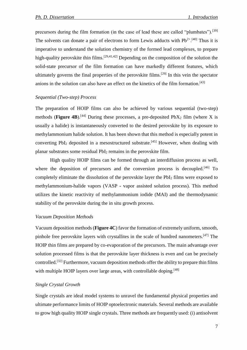
Ph. D. Dissertation 1. Introduction
7
precursors during the film formation (in the case of lead these are called “plumbates”).[39]
The solvents can donate a pair of electrons to form Lewis adducts with Pb2+.[40] Thus it is
imperative to understand the solution chemistry of the formed lead complexes, to prepare
high-quality perovskite thin films.[29,41,42] Depending on the composition of the solution the
solid-state precursor of the film formation can have markedly different features, which
ultimately governs the final properties of the perovskite films.[29] In this vein the spectator
anions in the solution can also have an effect on the kinetics of the film formation.[43]
Sequential (Two-step) Process
The preparation of HOIP films can also be achieved by various sequential (two-step)
methods (Figure 4B).[44] During these processes, a pre-deposited PbX2 film (where X is
usually a halide) is instantaneously converted to the desired perovskite by its exposure to
methylammonium halide solution. It has been shown that this method is especially potent in
converting PbI2 deposited in a mesostructured substrate.[45] However, when dealing with
planar substrates some residual PbI2 remains in the perovskite film.
High quality HOIP films can be formed through an interdiffusion process as well,
where the deposition of precursors and the conversion process is decoupled.[46] To
completely eliminate the dissolution of the perovskite layer the PbI2 films were exposed to
methylammonium-halide vapors (VASP - vapor assisted solution process). This method
utilizes the kinetic reactivity of methylammonium iodide (MAI) and the thermodynamic
stability of the perovskite during the in situ growth process.
Vacuum Deposition Methods
Vacuum deposition methods (Figure 4C) favor the formation of extremely uniform, smooth,
pinhole free perovskite layers with crystallites in the scale of hundred nanometers.[47] The
HOIP thin films are prepared by co-evaporation of the precursors. The main advantage over
solution processed films is that the perovskite layer thickness is even and can be precisely
controlled.[32] Furthermore, vacuum deposition methods offer the ability to prepare thin films
with multiple HOIP layers over large areas, with controllable doping.[48]
Single Crystal Growth
Single crystals are ideal model systems to unravel the fundamental physical properties and
ultimate performance limits of HOIP optoelectronic materials. Several methods are available
to grow high quality HOIP single crystals. Three methods are frequently used: (i) antisolvent
Ph. D. Dissertation 1. Introduction
8
vapor assisted,[49] (ii) cooling a saturated solution,[50] and (iii) retrograde solubility
approaches.[51–53]
An unusual property of many HOIPs is their loss of solubility upon heating, which is
termed retrograde solubility. This rare phenomenon is caused by the coordination of solvate
molecules and plumbates. The applicable solvent is different for each perovskite: MAPbCl3
– DMSO or DMSO/DMF mixture,[52] MAPbBr3 – DMF,[51] and MAPbI3 – GBL[51]. There
are two requirements to observe retrograde solubility in a solvent: the solvent should form
stable complexes with the plumbates in solution, and these complexes should dissociate at
elevated temperatures.
1.1.3. Optoelectronic Properties
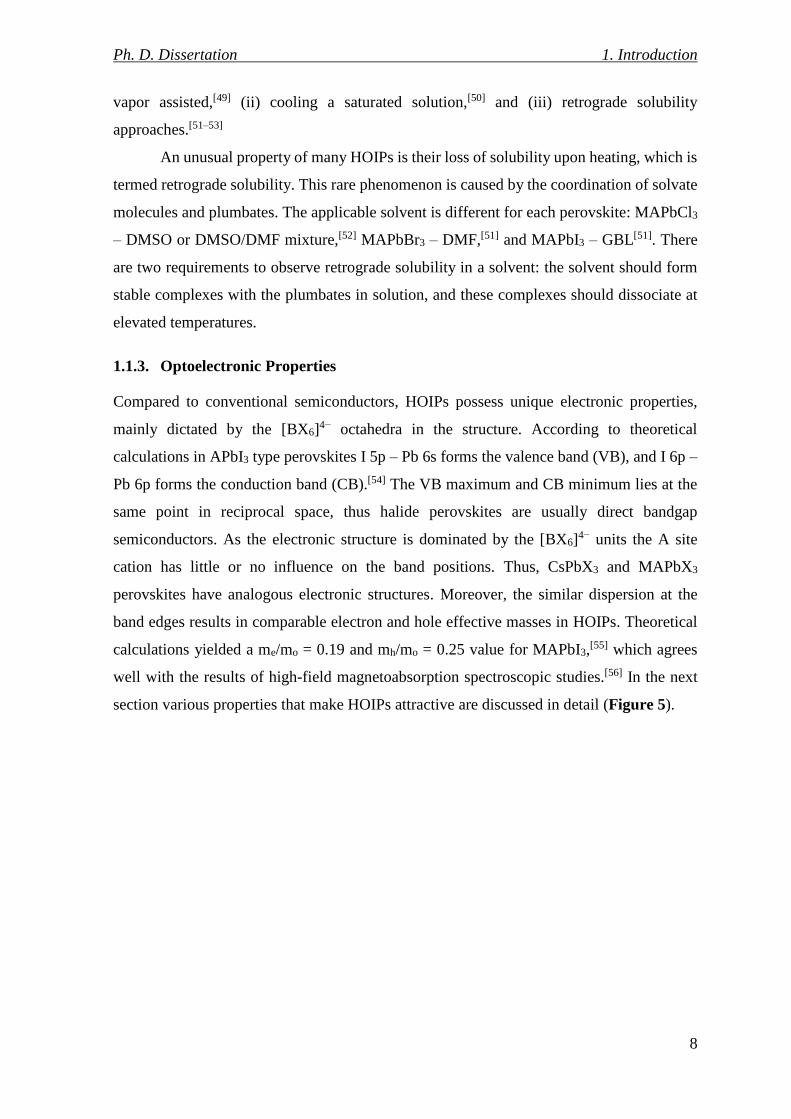
Compared to conventional semiconductors, HOIPs possess unique electronic properties,
mainly dictated by the [BX6]4− octahedra in the structure. According to theoretical
calculations in APbI3 type perovskites I 5p – Pb 6s forms the valence band (VB), and I 6p –
Pb 6p forms the conduction band (CB).[54] The VB maximum and CB minimum lies at the
same point in reciprocal space, thus halide perovskites are usually direct bandgap
semiconductors. As the electronic structure is dominated by the [BX6]4− units the A site
cation has little or no influence on the band positions. Thus, CsPbX3 and MAPbX3
perovskites have analogous electronic structures. Moreover, the similar dispersion at the
band edges results in comparable electron and hole effective masses in HOIPs. Theoretical
calculations yielded a me/mo = 0.19 and mh/mo = 0.25 value for MAPbI3,[55] which agrees
well with the results of high-field magnetoabsorption spectroscopic studies.[56] In the next
section various properties that make HOIPs attractive are discussed in detail (Figure 5).
Ph. D. Dissertation 1. Introduction
9
Figure 5. Summary of optoelectronic properties of HOIPs.
Large Absorption Coefficient
Efficient photovoltaic materials must possess a large absorption coefficient. This is
important for two reasons: it enables efficient light harvesting, and is a prerequisite for a
large open-circuit voltage (VOC) of a derived device. HOIPs are among the most efficient
light absorbers, as such MAPbI3 has an absorption coefficient greater than 3.0·104 cm−1 in
the visible region.[57,58] The strong absorption property of this materials family is attributed
to the coexistence of a direct bandgap and the metal p → halide p transition.[58] This p-p
optical transition is stronger than the p-s transition seen in other thin-film solar cell materials.
The cause of this is the lone pair effect of the B site metal, thus the CB of these perovskites
can be derived from the unoccupied p orbitals of the metal. These p orbitals have less
dispersion than s orbitals resulting in a greater density of states along the CB edges.[58]
Because of the large absorption coefficient, the active layer thickness in PSCs is in
the range of 0.3 – 0.6 m, which is three orders of magnitude thinner as in the case of silicon
solar cells. Apart from reducing material cost, this also impacts the magnitude of charge
carrier recombination in the devices. In thinner configurations, photogenerated carriers do
not have to travel far before they are collected, thus they are less prone to recombination.
This in turn affects the VOC of the derived devices.[57,59] Finally, we note that any distortion
in the crystal lattice can cause variation in the optical properties of perovskites. Therefore, it
is imperative to preserve the 3D B-X framework to achieve high efficiencies.
Ph. D. Dissertation 1. Introduction
10
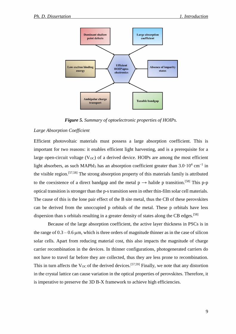
Absence of Impurity States
The steepness of the optical absorption edge of a material can be characterized by the Urbach
energy. Disorder of the microstructure or high density of deep traps can result in the
exponential curvature of the absorption near the edge. This sub-bandgap absorption can
contribute to VOC loss of a device. HOIPs possess small Urbach energy (MAPbI3 ~ 15 meV)
which further enhances their optoelectronic properties.[60] Furthermore, dramatic
improvement in device performance can be achieved through Cs+ incorporation, which
reduces the Urbach energy and in turn increases the maximum attainable VOC.[61,62]
Tunable Bandgap
The bandgap of HOIPs lies in the wavelength regime of visible light (1.2 eV – 3.0 eV).
Through simple modifications to the perovskite structure or composition the electronic
properties and thus the bandgap of these materials can be fine-tuned.
As theoretical calculations predicted, the A-site cation has negligible contribution to
the band structure of the HOIPs.[63] However, the incorporation of different sized cations
into the lattice can cause distortions in the perovskite framework, which in turn have an
effect on the electronic properties of the material.[64–66] The most prominent feature is that
through mixing A-site cations phase stabilization of elusive perovskite phases can be
achieved (as seen in the case of -FAPbX3). [61,67,68]
The B-site cation is one of the fundamental elements that govern the electronic
structure of perovskites. Any exchange on this site leaves the perovskite framework and
lattice parameters intact. Through the gradual Sn(II)-Pb(II) exchange in MAPb1−xSnxI3
continuous variation of the optoelectronic properties was achieved (Eg = 1.17 – 1.55 eV).[69–
71] Interestingly, this exchange shows deviation from Vegard’s law. Namely, the bandgap of
the solid solutions is not a linear function of composition (lattice parameter). The mixed
compositions all showed lower bandgap values compared to the pure compounds.[71]
X-site anion exchange has the most prominent effect on the optical properties of
HOIPs. In mixed-halide compounds the bandgap monotonously decreases in the series of
Cl− > Br− > I−. By gradually varying the anion composition of CsPbClxBr3−x and CsPbBrxI3−x
nanocrystals their photoluminescence can be precisely tuned between 400-700 nm.[72,73] A
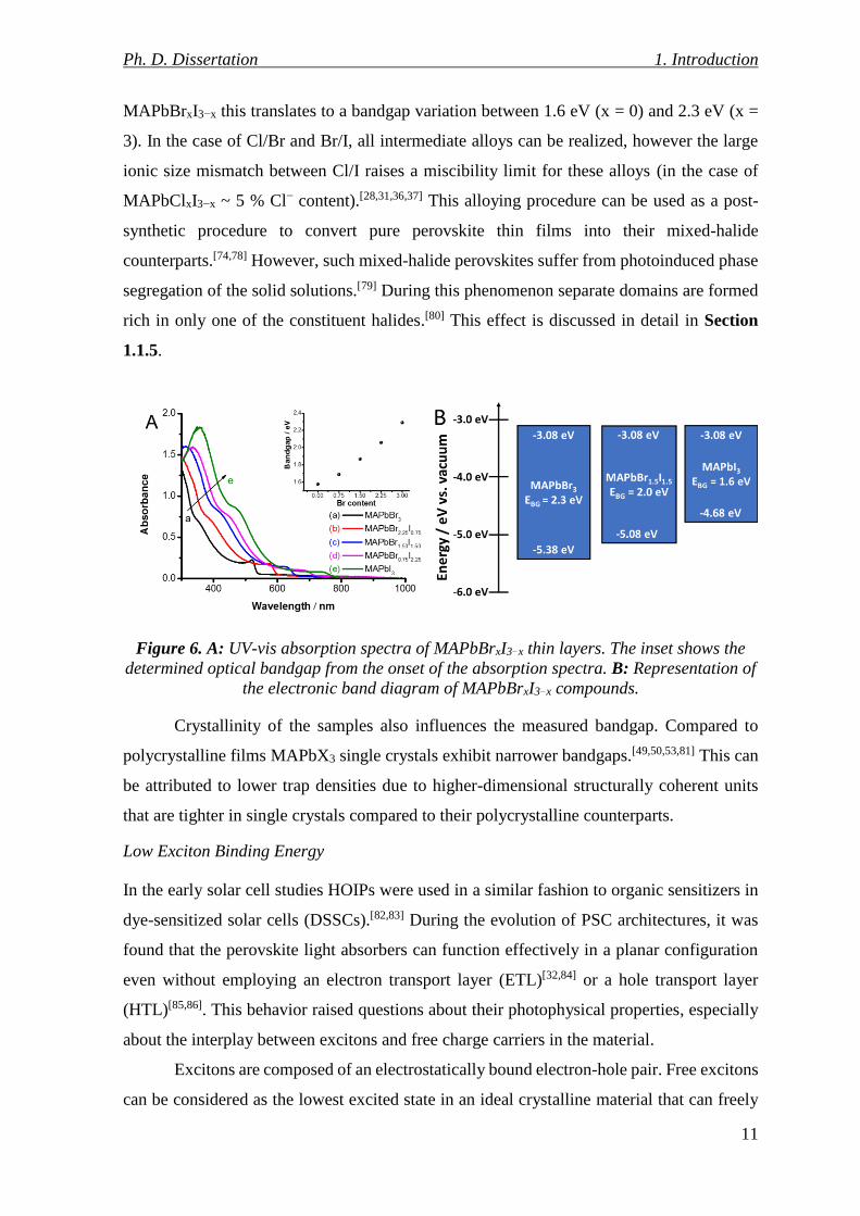
similar bandgap tunability was found for MAPbClxBr3−x and MAPbBrxI3−x (Figure 6A) as
well.[74–77] This substitution mainly affects the VB position of the compounds, as the halide
p orbitals have a large contribution to the VB of perovskites (Figure 6B). In the case of
Ph. D. Dissertation 1. Introduction
11
MAPbBrxI3−x this translates to a bandgap variation between 1.6 eV (x = 0) and 2.3 eV (x =
3). In the case of Cl/Br and Br/I, all intermediate alloys can be realized, however the large
ionic size mismatch between Cl/I raises a miscibility limit for these alloys (in the case of
MAPbClxI3−x ~ 5 % Cl− content).[28,31,36,37] This alloying procedure can be used as a post-
synthetic procedure to convert pure perovskite thin films into their mixed-halide
counterparts.[74,78] However, such mixed-halide perovskites suffer from photoinduced phase
segregation of the solid solutions.[79] During this phenomenon separate domains are formed
rich in only one of the constituent halides.[80] This effect is discussed in detail in Section
1.1.5.
Figure 6. A: UV-vis absorption spectra of MAPbBrxI3−x thin layers. The inset shows the
determined optical bandgap from the onset of the absorption spectra. B: Representation of
the electronic band diagram of MAPbBrxI3−x compounds.
Crystallinity of the samples also influences the measured bandgap. Compared to
polycrystalline films MAPbX3 single crystals exhibit narrower bandgaps.[49,50,53,81] This can
be attributed to lower trap densities due to higher-dimensional structurally coherent units
that are tighter in single crystals compared to their polycrystalline counterparts.
Low Exciton Binding Energy
In the early solar cell studies HOIPs were used in a similar fashion to organic sensitizers in
dye-sensitized solar cells (DSSCs).[82,83] During the evolution of PSC architectures, it was
found that the perovskite light absorbers can function effectively in a planar configuration
even without employing an electron transport layer (ETL)[32,84] or a hole transport layer
(HTL)[85,86]. This behavior raised questions about their photophysical properties, especially
about the interplay between excitons and free charge carriers in the material.
Excitons are composed of an electrostatically bound electron-hole pair. Free excitons
can be considered as the lowest excited state in an ideal crystalline material that can freely
Ph. D. Dissertation 1. Introduction
12
move through the lattice, without the transfer of a net charge. The ionization of an exciton
to separate charge carriers is thus a crucial aspect in optimizing photovoltaic devices (carrier
extraction). For MAPbI3 low binding energy (Mott-Wannier type) excitons are predicted.[19]
These can easily dissociate, thus numeric simulations suggest that free charge carriers
dominate these materials.[87] It has been shown that the charge carrier generation for both
MAPbI3 and MAPbBr3 shows non-excitonic bevavior.[88,89] Furthermore, the external
quantum efficiency of MAPbBr3 based devices is unaffected by the use of an external
electrical field, which would have an effect if the charge carrier generation in these materials
were excitonic in nature.[89]
Ambipolar Charge Transport
The small effective mass of electrons and holes in MAPbI3 signals high charge carrier
mobility (inverse relationship).[19,90] Furthermore, the fact that PSCs can function without
the use of specific ETL[32,84] or HTL[85,86] also indicates good ambipolar electron and hole
transport property of the material. This notion was confirmed by quenching experiments,
where selective electron and hole extraction was achieved. The electron-hole diffusion
length was in the range of ~100 nm in solution processed MAPbBr3 and MAPbI3.[91,92] The
investigation of MAPbI3 single crystals revealed a charge carrier diffusion length of ~ 8-10
micrometers.[49,51] Currently, the record is held by mm thick MAPbI3 single crystals, where
charge carrier diffusion lengths greater than 175 m under 1 sun illumination were shown.[93]
This long-ranged, balanced charge carrier diffusion can be considered a general property of
HOIP single crystals as the diffusion length is ~9 m in MAPbCl3,[52] and is ~4-17 m in
MaPbBr3[49,51].
The reason for the long charge carrier diffusion length lies in the rate of different
recombination scenarios (Figure 7) in the perovskite layer.[19,90,94,95] Both monomolecular
(first-order, i.e., geminate recombination of exciton and trap- or impurity-assisted
recombination) and bimolecular (second-order) recombination rates are extremely low in
HOIPs. Although Auger recombination (third-order) rates were found to be high, however
this recombination pathway is only dominant at high light intensities.[96]

Ph. D. Dissertation 1. Introduction
13
Figure 7. Schematic representation of the various photophysical processes in perovskites
following photoexcitation. Adapted from ref.[90].
Dominant Shallow Point Defects
One of the key features that allows perovskites to deliver remarkable solar cell efficiencies
is their unique defect tolerance.[97,98] Defect states in a semiconductor can promote
recombination processes, and act as scattering centers for free-charge carriers, thus they
deleteriously influence the overall charge collection process.[99] Most HOIPs are fabricated
through low-temperature solution processes and still possess small trap densities. The bulk
trap density in polycrystalline perovskite thin-films is ~1015 – 1017 cm−3, which becomes
even lower ~ 1010 cm−3 in perovskite single crystals.[49,81] In comparison, the trap density of
polycrystalline silicon: ~1015 cm−3,[100] GaAs: ~1017 cm−3,[101] TiO2: ~1017 cm−3.[102] This low
Ph. D. Dissertation 1. Introduction
14
trap density in polycrystalline perovskite thin films can be attributed to their low
crystallization activation energy barrier.
Based on the large difference between trap densities of polycrystalline and single
crystal perovskites, interfaces and grain boundaries can also act as extended defects. This is
mainly caused by the altered stoichiometry of the material on the surface. This holds true for
the surface of single crystals as well.[103] Furthermore, the measured defect density is proved
to be facet-dependent.[104] To alleviate surface traps, tuning the synthesis conditions to
achieve preferred grain orientation or post-synthesis surface passivation strategies are
employed.[105] Although theoretical calculations suggest that grain boundaries are inherently
benign, and they do not generate gap states, making polycrystalline perovskites single crystal
like,[58] the exact nature of grain boundaries in PSCs remains an open question to be
answered.
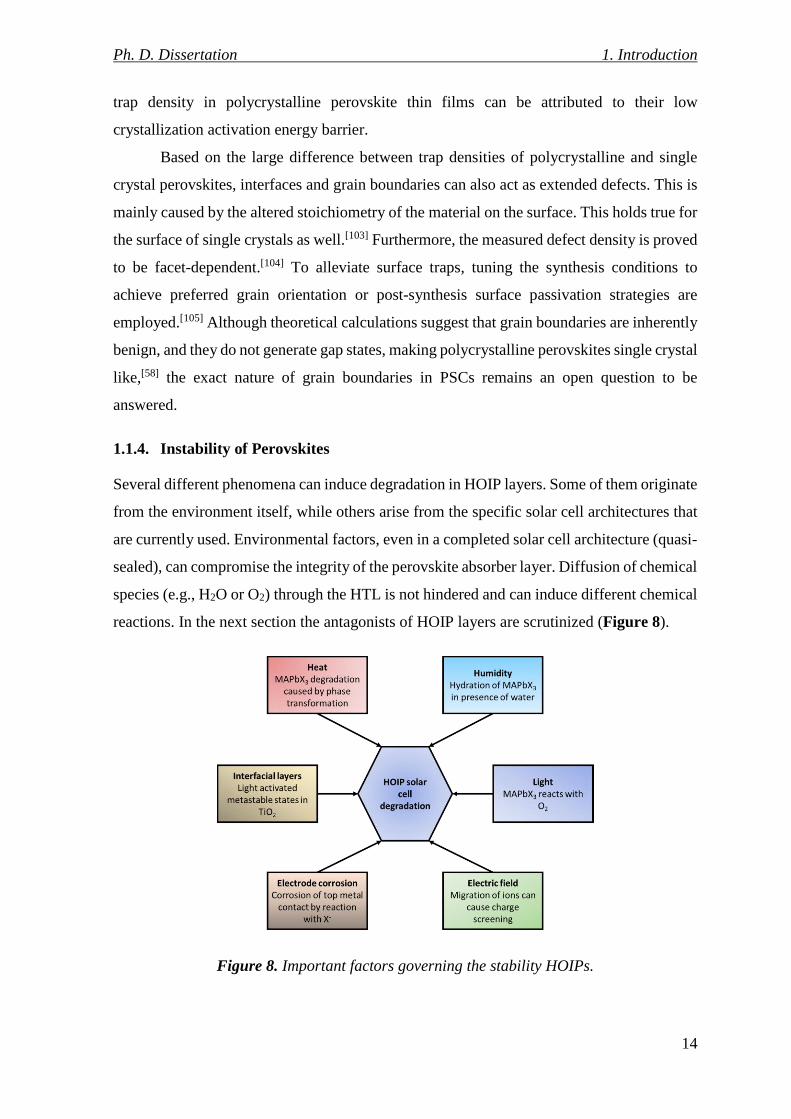
1.1.4. Instability of Perovskites
Several different phenomena can induce degradation in HOIP layers. Some of them originate
from the environment itself, while others arise from the specific solar cell architectures that
are currently used. Environmental factors, even in a completed solar cell architecture (quasi-
sealed), can compromise the integrity of the perovskite absorber layer. Diffusion of chemical
species (e.g., H2O or O2) through the HTL is not hindered and can induce different chemical
reactions. In the next section the antagonists of HOIP layers are scrutinized (Figure 8).
Figure 8. Important factors governing the stability HOIPs.
Ph. D. Dissertation 1. Introduction
15
Effect of Humidity
Perhaps the Achilles heel of HOIPs is their sensitivity to polar solvents, especially
water.[41,106–110] The overall reaction for the degradation of MAPbI3 is described by Eq. 3 as:
𝐶𝐻3𝑁𝐻3𝑃𝑏𝐼3(𝑠) → 𝐶𝐻3𝑁𝐻2(𝑔) + 𝐻𝐼(𝑔) + 𝑃𝑏𝐼2(𝑠) (3)
However, the actual decomposition reaction is more complex with multiple intermediate
hydrated species.[106–108] This alteration affects the light absorption characteristics and
induces morphological changes, where the perovskite crystals smoothen and become more
oriented.[106,107] The detailed mechanism is described by Eq. 4-5. As the first step, hydrogen
bonding between water molecules and the MA+ in the lattice disrupts the 3D perovskite
framework. As a result, the structure is gradually transformed into lower dimensional
perovskite structures. First 2D perovskite sheets are formed that are separated by water,
which leads to the formation of isolated [PbI6]4− octahedral units. The first step, where
MAPbI3·H2O is formed, is completely reversible.[108]
4𝐶𝐻3𝑁𝐻3𝑃𝑏𝐼3 + 4𝐻2𝑂 ⇌ 4[𝐶𝐻3𝑁𝐻3𝑃𝑏𝐼3 ∙ 𝐻2𝑂] (4)
4[𝐶𝐻3𝑁𝐻3𝑃𝑏𝐼3 ∙ 𝐻2𝑂] ⇌ (𝐶𝐻3𝑁𝐻3)4𝑃𝑏𝐼6 ∙ 2𝐻2𝑂 + 3𝑃𝑏𝐼2 + 2𝐻2𝑂 (5)
Under ambient conditions, the formation of alternative degradation products other than PbI2
was also confirmed. During the destruction of the 3D perovskite structure the presence of
amorphous -PbO, PbCO3, and Pb(OH)2 was also shown.[110] In a similar manner, ammonia
vapor can also rapidly degrade the MAPbI3 phase.[111] The nature of the halide in the
perovskite structure affects the overall water sensitivity of the compound, which increases
in the Cl− < Br− < I− order. The mixing of a more moisture resistant halide to a sensitive
system can improve the stability of the formed perovskite, however at the expense of device
efficiency.[77]
Effect of Light
It has been found that illumination even in the absence of moisture can degrade MAPbI3.[112–
114] The proposed mechanism is described by Eq. 6-8. As a first step MAPbI3 is excited and
photogenerated electrons and holes are formed. Electrons from the CB of MAPbI3 can be
transferred to adsorbed oxygen on the surface, thus forming superoxide anions. The formed
superoxide can simultaneously deprotonate MA+ and oxidize I−, thus compromising the
stability. Note that the formation of water in Eq. 8 can initiate previously described
Ph. D. Dissertation 1. Introduction
16
degradation pathways. As expected, however perovskite films stored in nitrogen were stable
under steady state illumination.[112–114]
𝐶𝐻3𝑁𝐻3𝑃𝑏𝐼3 ℎ𝜈 > 𝐸𝑔→ 𝐶𝐻3𝑁𝐻3𝑃𝑏𝐼3
∗ (6)
𝑂2 𝐶𝐻3𝑁𝐻3𝑃𝑏𝐼3
∗
→ 𝑂2∙− (7)
𝑂2∙− + 𝐶𝐻3𝑁𝐻3𝑃𝑏𝐼3⟶ 𝐶𝐻3𝑁𝐻2 + 𝑃𝑏𝐼2 + 0.5𝐼2 + 𝐻2𝑂 (8)
It was observed that the degradation reaction is more rapid when Al2O3 is used as the
mesoporous scaffold (instead of TiO2).[112–114] Thus, the use of TiO2 can suppress this
decomposition, by extracting the formed electrons from the MAPbI3 surface before they can
react with the adsorbed oxygen. The opposite effect can also be achieved when MAPbI3
layers are forward biased in the dark and in the presence of O2.[114] Under these
circumstances electrons are injected into the MAPbI3 layer which initiate the rapid
deterioration of the active layer.
Effect of Heat
It is crucial to assess the thermal stability of HOIPs layers for two distinct reasons: to
optimize the annealing temperature during film deposition, and to ensure device stability
during operation.[109,115]
During preparation the perovskite films are annealed for a brief amount of time at
moderately high temperatures in the ~100 °C regime. This removes any excess solvent or
additive that would remain in the film. Furthermore, it facilitates the formation of the
perovskite crystal structure and ensures a proper coverage. In this sense a balance must be
found to remove all residual materials, without the degradation of the perovskite material.
However, the thermal stability of MAPbI3 seems somewhat controversial.
Thermogravimetric studies suggest that MAPbI3 decomposes at ~300 °C.[50,116–118] A weight
loss is observed between 270 and 340 °C and is attributed to the removal of organic
components from the structure (i.e., CH3NH3I or CH3NH2 together with HI). Furthermore,
MAPbI3 undergoes a tetragonal-cubic phase transition at 56 °C,[119] which greatly limits its
application in functioning devices. These issues motivated the exchange of MA+ to FA+ in
the perovskite lattice, to enhance its thermal stability.[67,120]
Ph. D. Dissertation 1. Introduction
17
Interfacial Layers
The obvious sensitivity issues regarding HOIPs has drawn the attention away from the other
constituents of the PSC architecture. The most commonly used ETL (TiO2) was found to be
a major contributor to the instability of PSCs.[121] UV-light irradiated solar cells suffered
from rapid deterioration of their efficiency which was related to a drop in their charge
collection efficiency. Ultimately, this phenomenon was explained by the formation of deep
trap states within the mesoporous TiO2 framework caused by the UV irradiation.[121] When
a UV-cutoff filter or Al2O3 was used as the scaffold, this problem disappeared. The
deterioration of PSC performance is also related to adsorbed molecular O2, connected to
oxygen vacancies in the TiO2 framework (Ti3+ ions), which leads to the formation of Ti4+-
O2− charge-transfer complexes. Upon UV excitation, the superoxide radical is oxidized by
the photogenerated holes, leading to the desorption of molecular oxygen and the formation
of a partially occupied deep trap state in TiO2.[121]
Similarly, the HTL also poses a threat to the stability of PSCs. The additives used in
the deposition of the most common hole transport material (HTM) 2,2′,7,7′-tetrakis(N,N′-
di-p-methoxyphenylamine)-9,9′-spirobifluorene (spiro-MeOTAD), can also cause the
degradation of the solar cell device. It was shown that in the case of DSSCs 4-tert-
butylpyridine can evaporate from devices at low temperatures (~85 °C).[122] Furthermore,
Li-bis(trifluoromethane)-sulfonimide (Li-TFSI), the material used to improve the
conductivity of the spiro-MeOTAD layer, is a deliquescent material and can draw moisture
from the air into the device.
Electrode Corrosion
In completely assembled PSC architectures, it was found that corrosion of the metal top
contact can also negatively influence the stability of PSCs. In cases where Ag was used,
discoloration of the top contact was observed after several days.[123] This can be attributed
to the migration of iodide ions through the HTL to the Ag contact, where the formation of
AgI occurs. This issue also affects other type of top contacts (e.g., Ca, Al, Cr/Cr2O3).[124]
Interestingly, Au as a top contact is also prone to such corrosion events.[124,125]
The Effect of Electric Fields
Perovskites, especially CsPbBr3 and CsPbI3, are well known ionic conductors, as the
activation energy for the migration of the halide-ion vacancy is low.[126] In HOIPs there are
several candidates for the migrating species. All perovskite forming ions can participate (in
Ph. D. Dissertation 1. Introduction
18
the case of MAPbI3 e.g., MA+, Pb2+ and I−) in the overall migration process. Furthermore,
additional species from the decomposition scenarios should be also considered (H+).[127] The
likelihood of ion migration (i.e., activation energy of migration) depends on several factors:
(i) size of the drifting ion, (ii) distance of the vacancy from the ion, (iii) charge of ions and
(iv) crystal structure of the material. Theoretical studies agree that the probability of
migration follows the I− > MA+ > Pb2+ trend. In materials with the ABX3 perovskite
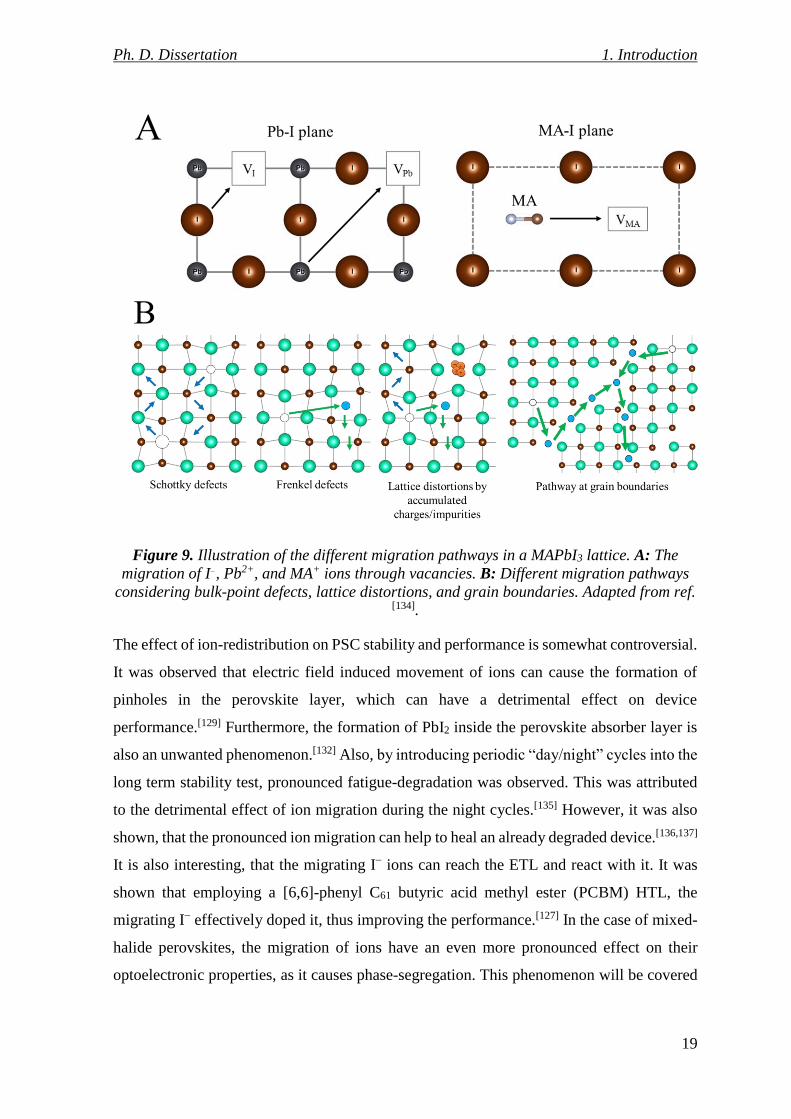
structure, the vacancy-mediated diffusion process is the most common (Figure 9A).
Experimental studies suggest the dominance of electric field induced migration of MA+ and
I− ions. A redistribution of MA+ occurred when a lateral MAPbI3 solar cell was electrically
biased.[127–129] After applying a small electrical field, the MA+ ions accumulated in the
cathode region and were depleted in the anode and central region of the cell. This phenomena
led to a switchable photovoltaic effect in such devices. [127–129] The case of I− migration
seemed to be a more elusive problem. At elevated temperatures, the movement of I− through
interstitial vacancies was shown.[130] I− migration in a Pb-anode/MAPbI3/AgI/Ag-cathode
arrangement was also the cause of the formation of PbI2 layer near the Pb anode.[131] It was
also demonstrated that at elevated temperatures the use of electrical bias in a lateral MAPbI3
cell can cause the formation of a thin PbI2 layer in the middle of the cell. The electric field
driven movement of this PbI2 layer was explained by the massive movement of I− and MA+
ions.[132] There are several ion-migration pathways that can participate in the overall process
(summarized in Figure 9B). Not just point defects, but bulk defects, surface and grain
boundaries play an important role in ion migration. The grain size of the perovskite films
has a pronounced effect on the extent of ion migration.[129,133] It is more difficult to induce
photovoltaic switching in PSCs with large grains and this property is directly proportional
to the extent of migration in the layer.[129]
Ph. D. Dissertation 1. Introduction
19
Figure 9. Illustration of the different migration pathways in a MAPbI3 lattice. A: The
migration of I−, Pb2+, and MA+ ions through vacancies. B: Different migration pathways
considering bulk-point defects, lattice distortions, and grain boundaries. Adapted from ref. [134].
The effect of ion-redistribution on PSC stability and performance is somewhat controversial.
It was observed that electric field induced movement of ions can cause the formation of
pinholes in the perovskite layer, which can have a detrimental effect on device
performance.[129] Furthermore, the formation of PbI2 inside the perovskite absorber layer is
also an unwanted phenomenon.[132] Also, by introducing periodic “day/night” cycles into the
long term stability test, pronounced fatigue-degradation was observed. This was attributed
to the detrimental effect of ion migration during the night cycles.[135] However, it was also
shown, that the pronounced ion migration can help to heal an already degraded device.[136,137]
It is also interesting, that the migrating I− ions can reach the ETL and react with it. It was
shown that employing a [6,6]-phenyl C61 butyric acid methyl ester (PCBM) HTL, the
migrating I− effectively doped it, thus improving the performance.[127] In the case of mixed-
halide perovskites, the migration of ions have an even more pronounced effect on their
optoelectronic properties, as it causes phase-segregation. This phenomenon will be covered
Ph. D. Dissertation 1. Introduction
20
thoroughly in Section 1.1.5. It is also worth mentioning that electric field induced ionic
migration is the main cause of the severe current-voltage hysteresis experienced in PSCs.[138]
1.1.5. Light-Induced Phase Segregation in Mixed Halide Perovskites
The ability to tune the bandgap of mixed halide perovskites through halide composition is
an attractive strategy to design solar cells with tailored response.[61,63,139] Several research
groups have evaluated solar cell performance under short-term irradiation and they
considered the photovoltaic performance to be stable.[140] Halide ion migration in PSCs plays
an important role in determining the overall photovoltaic performance.[141–143] Light soaking,
for example, leads to migration of ions and vacancies toward the oxide interface influencing
the observed photovoltage.[144] Another property of the mixed halide lead perovskite is its
ability to undergo phase segregation under continuous illumination.[80,140,145–148] For
example, when MAPbX3 (X = Br, I, 1:1 ratio) is subjected to long-term (> 20 min) visible-
light irradiation, it undergoes phase segregation to yield iodide rich and bromide rich
domains as described by Eq. 9.
𝑛 𝑀𝐴𝑃𝑏𝐵𝑟𝑥𝐼3−𝑥 + ℎ𝜈 →
(𝑛 − 2𝑚) 𝑀𝐴𝑃𝑏𝐵𝑟𝑥𝐼3−𝑥 +𝑚 𝑀𝐴𝑃𝑏𝐵𝑟𝑥−𝑦𝐼3−𝑥+𝑦 +𝑚 𝑀𝐴𝑃𝑏𝐵𝑟𝑥+𝑦𝐼3−𝑥−𝑦 (9)
Upon stopping the illumination, the segregated phases are restored to the original
mixed phase.[147–149] In previous studies, the kinetics of halide ion segregation as well as dark
recovery was monitored. The origin of the segregation has been explained using different
models. These include entropy of mixing,[145] halide ion defect driven movement of ions,[150]
and polaron induced lattice strain.[149] It was also found that the excitation intensity and
duration of irradiation determines the dark recovery.[147,150] However, up to this point the
effect of halide ion segregation on the performance of PSCs was missing. This raises the
obvious question: What is the impact of long-term light irradiation (or light soaking) on the
performance of mixed halide perovskite solar cells?
1.1.6. Electrochemical Properties of Perovskites
In unraveling the reasons behind the unparalleled optoelectronic properties of HOIPs the use
of (photo)electrochemical techniques started to gain a foothold recently. These powerful
tools are capable of probing charge carrier generation and transport in HOIPs. Fundamental
optoelectronic properties (e.g., band edge positions, distribution of trap states) can be probed
Ph. D. Dissertation 1. Introduction
21
using spectroelectrochemistry. Furthermore, the use of other coupled techniques can
contribute to the understanding the chemical changes at the interfaces and in the electrode
material itself upon charge carrier generation. The use of electrochemical techniques is not
restricted to probing physicochemical properties of HOIPs but can also be used as a synthetic
tool in the assembly of complex perovskite architectures. Electrochemistry can even be
invoked as a possible lead removal strategy in HOIP recycling scenarios.[151]
The extreme sensitivity of HOIPs to polar solvents made all electrochemical
measurements rather challenging. Recently, it was demonstrated that (photo)electrochemical
measurements can be performed in dichloromethane-based electrolytes in the presence of
different reversible redox couples (e.g., ferrocene and benzoquinone).[152] The assembled
liquid junction cells showed remarkable stability for prolonged irradiation. In this notion,
electrochemical impedance analysis was performed to estimate the flatband potential and
charge carrier density of different HOIPs.[152,153] A very thorough study investigated the
electron injection process into formamidinium lead halide perovskite using
spectroelectrochemistry.[154] It was demonstrated in this study that it is very difficult, yet
possible, to probe band edge positions via charge carrier injection. During these experiments,
however, an irreversible electrochemical reduction occurred, thus making the picture even
murkier. An overview of the possible solution chemistry events was given, although without
taking into account the likely contribution of the electrolyte ions.[154] A similar approach was
followed for mixed CsPbX3 (X = Cl−, Br−, and I−) perovskites, where it was assumed that
band edge positions can be simply determined from voltammetric data.[155]
Apart from determining various physicochemical properties, coupled
(photo)electrochemical techniques can offer a fast and convenient way to perform
combinatorial analysis of the performance of various HOIP compositions. Scanning
electrochemical microscopy can be effectively used to determine the optimal composition
of different perovskite compounds in a semiconductor array arrangement.[156,157] In terms of
delivering the highest photocurrent, the optimal excess PbI2 content of MAPbI3 layers[156]
and the optimal MASnI3−xBrx composition[157] were determined in a liquid junction setup.
By encapsulating the HOIP layer in a photoelectrode assembly, their use as efficient
photocathodes in H2 generation in aqueous media was also shown.[158] The photocathodes
retained more than 80 % of their efficiency for ~1 h. The effective protection of the HOIP
electrode can pave the way of using these materials in solar fuel generation scenarios.[159]

Ph. D. Dissertation 1. Introduction
22
Li-ion Batteries
Halide perovskites of the CsPbX3 family can be considered as fast ionic conductors, because
of their high ionic conductivity.[126] This means that their crystal structure remains rather
frozen, while ionic species are migrating through the lattice. The complex defect chemistry
makes it difficult to discern the diffusivity of specific ions through the perovskite lattice.
However, an extrinsic Li+ source (e.g., through a solution/perovskite interface) can be used
to determine ionic diffusion kinetics in HOIPs.[160] In such a case, electronic and ionic
transport is decoupled, because the migration and intercalation of Li+ (the slower process)
determines the kinetics of the diffusion process. In highly lithiated 3D MAPbBr3 electrodes
the ionic conductivity was found to be 10−3 −1 cm−1, which falls in the range of superionic
conductors (10−4 −1 cm−1 – 10−1 −1 cm−1). As the perovskite lithiation progresses, specific
capacity values as high as 400 mA h g−1 were reached.[160,161] 3D MaPbBr3 electrodes exhibit
a highly reversible lithium uptake and release without severe distortion of the perovskite
lattice (topotactic intercalation). It was proposed that the lithiation proceeds in a fashion that
multiple Li+ are intercalated into the same unit cell. In this sense, the formation of
LixMAPbBr3 compounds were assumed, where x approaches 3. MAPbI3 has inferior specific
capacitance and stability compared to MAPbBr3 based electrodes. A summary of specific
capacitance values can be seen in Table 1. All specific capacitance values for the first
discharge cycle greatly surpass the theoretical limit for MAPbBr3 (56 mA h g−1), which
raises suspicion that a conversion event or another effect is also in play.[162] Furthermore,
these results are often not supported by any intercalation mechanism. Theoretical
calculations and experimental results suggest that in the case of MAPbCl3 and MAPbBr3 the
conversion process to LiX and Pb metal dominates the electrochemical behavior.[162]
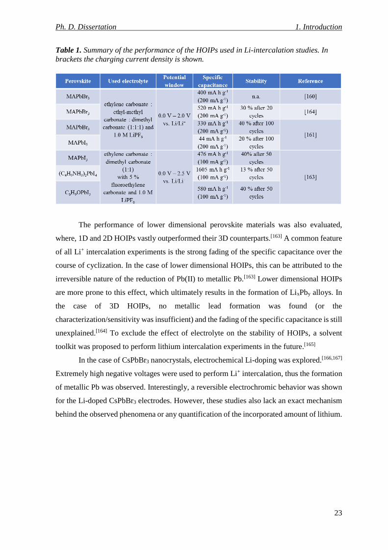
Ph. D. Dissertation 1. Introduction
23
Table 1. Summary of the performance of the HOIPs used in Li-intercalation studies. In
brackets the charging current density is shown.
The performance of lower dimensional perovskite materials was also evaluated,
where, 1D and 2D HOIPs vastly outperformed their 3D counterparts.[163] A common feature
of all Li+ intercalation experiments is the strong fading of the specific capacitance over the
course of cyclization. In the case of lower dimensional HOIPs, this can be attributed to the
irreversible nature of the reduction of Pb(II) to metallic Pb.[163] Lower dimensional HOIPs
are more prone to this effect, which ultimately results in the formation of LixPby alloys. In
the case of 3D HOIPs, no metallic lead formation was found (or the
characterization/sensitivity was insufficient) and the fading of the specific capacitance is still
unexplained.[164] To exclude the effect of electrolyte on the stability of HOIPs, a solvent
toolkit was proposed to perform lithium intercalation experiments in the future.[165]
In the case of CsPbBr3 nanocrystals, electrochemical Li-doping was explored.[166,167]
Extremely high negative voltages were used to perform Li+ intercalation, thus the formation
of metallic Pb was observed. Interestingly, a reversible electrochromic behavior was shown
for the Li-doped CsPbBr3 electrodes. However, these studies also lack an exact mechanism
behind the observed phenomena or any quantification of the incorporated amount of lithium.
Ph. D. Dissertation 1. Introduction
24
Electrochemiluminescence
Electrochemiluminescence (ECL) could be employed to investigate charge carrier transfer
under various electrochemical conditions. Most studies on this matter focus exclusively on
understanding the properties of CsPbBr3. Several irreversible redox processes were
identified by cyclic voltammetry for CsPbBr3 nanocrystal (NC) based electrodes.[168,169] All
of these were attributed to the presence of charged states of the NCs. However, this
assumption is quite problematic, because it completely disregards the possibility of chemical
change (Faradaic processes) of the CsPbBr3 NCs. Electrochemically generated electrons and
holes were injected in rapid succession into the CsPbBr3 NC electrodes and the annihilation
of the ECL signal was monitored. This was performed by potential switching experiments,
where the potential of the CsPbBr3 NC electrodes was switched rapidly between an electron
injecting potential to a hole injecting potential. Relatively weak and fading ECL signals were
observed, which were attributed to the unstable nature of the radicals from CsPbBr3.[168]
However, this phenomenon more likely signals the chemical change of the perovskite layer.
An increased stability was observed when ethyl-acetate was used as the solvent. It was
proposed that ethyl-acetate can act as a co-reactant in the ECL reaction.[169]
ECL of both MAPbBr3[170] and CsPbBr3
[171] were studied in aqueous media as well,
but the stability of the films was not addressed. In a recent study, long carbon chain acids or
amids were used to stabilize CsPbBr3 NCs in aqueous media.[172] These ligands orient
themselves with their polar head groups, making the surface of the perovskite NCs surface
hydrophobic. This strategy was found to stabilize the CsPbBr3 NCs in aqueous media for a
few hours, but the degradation of the layers was still inevitable.
Despite the above examples, solid and coherent knowledge about the fundamental
electrochemical behavior of these materials is still missing. In this notion several questions
remain unanswered: What is the electrochemical window to safely conduct electrochemical
experiments and what are the redox events that were left unexplained?
1.2. Perovskite Solar Cells
Long-term device instability is the most pressing issue that hampers PSC commercialization.
As more effort was put into understanding the fundamental properties of HOIPs, better
control over device stability was achieved. It is imperative that apart from the degradation
of HOIPs, the role of the interfaces in the devices must be precisely evaluated. Each interface
and contact layer in the device plays a crucial role in determining the overall stability. When

Ph. D. Dissertation 1. Introduction
25
control over the interfaces is achieved, the devices will be absent from the initial rapid decay
(often termed burn-in) and the gradual slower decay of their efficiency.[173] Few studies
already reported extremely durable PSCs with over 1000 hours of continuous operation
without substantial decay, under ambient conditions (combined stresses of light (including
UV light), oxygen and moisture). [173–175]
1.2.1. General Solar Cell Architectures
To understand how different optoelectronic properties of HOIPs shaped the applicable solar
cell architectures a quick overview on the evolution PSCs is presented in the following
section (Figure 10).[176]
Figure 10. The evolution of PSC architectures. Adapted from ref.[176].
Three components are necessary to fabricate DSSCs: (i) a mesoporous n-type
semiconductor scaffold (e.g., TiO2), (ii) a light absorber (or sensitizer) anchored on the
surface of the scaffold (e.g. organic dyes, inorganic quantum dots), and (iii) a redox active
electrolyte (e.g., I2/I3−).[177] In these architectures it is imperative to use a high surface area
mesoporous scaffold. This ensures that sufficient amount of sensitizer can be adsorbed on
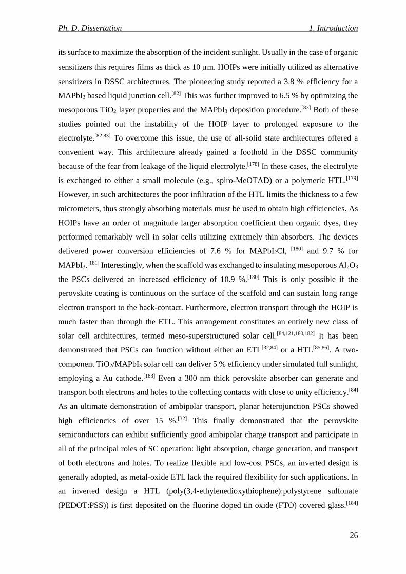
Ph. D. Dissertation 1. Introduction
26
its surface to maximize the absorption of the incident sunlight. Usually in the case of organic
sensitizers this requires films as thick as 10 m. HOIPs were initially utilized as alternative
sensitizers in DSSC architectures. The pioneering study reported a 3.8 % efficiency for a
MAPbI3 based liquid junction cell.[82] This was further improved to 6.5 % by optimizing the
mesoporous TiO2 layer properties and the MAPbI3 deposition procedure.[83] Both of these
studies pointed out the instability of the HOIP layer to prolonged exposure to the
electrolyte.[82,83] To overcome this issue, the use of all-solid state architectures offered a
convenient way. This architecture already gained a foothold in the DSSC community
because of the fear from leakage of the liquid electrolyte.[178] In these cases, the electrolyte
is exchanged to either a small molecule (e.g., spiro-MeOTAD) or a polymeric HTL.[179]
However, in such architectures the poor infiltration of the HTL limits the thickness to a few
micrometers, thus strongly absorbing materials must be used to obtain high efficiencies. As
HOIPs have an order of magnitude larger absorption coefficient then organic dyes, they
performed remarkably well in solar cells utilizing extremely thin absorbers. The devices
delivered power conversion efficiencies of 7.6 % for MAPbI2Cl, [180] and 9.7 % for
MAPbI3.[181] Interestingly, when the scaffold was exchanged to insulating mesoporous Al2O3
the PSCs delivered an increased efficiency of 10.9 %.[180] This is only possible if the
perovskite coating is continuous on the surface of the scaffold and can sustain long range
electron transport to the back-contact. Furthermore, electron transport through the HOIP is
much faster than through the ETL. This arrangement constitutes an entirely new class of
solar cell architectures, termed meso-superstructured solar cell.[84,121,180,182] It has been
demonstrated that PSCs can function without either an ETL[32,84] or a HTL[85,86]. A two-
component TiO2/MAPbI3 solar cell can deliver 5 % efficiency under simulated full sunlight,
employing a Au cathode.[183] Even a 300 nm thick perovskite absorber can generate and
transport both electrons and holes to the collecting contacts with close to unity efficiency.[84]
As an ultimate demonstration of ambipolar transport, planar heterojunction PSCs showed
high efficiencies of over 15 %.[32] This finally demonstrated that the perovskite
semiconductors can exhibit sufficiently good ambipolar charge transport and participate in
all of the principal roles of SC operation: light absorption, charge generation, and transport
of both electrons and holes. To realize flexible and low-cost PSCs, an inverted design is
generally adopted, as metal-oxide ETL lack the required flexibility for such applications. In
an inverted design a HTL (poly(3,4-ethylenedioxythiophene):polystyrene sulfonate
(PEDOT:PSS)) is first deposited on the fluorine doped tin oxide (FTO) covered glass.[184]
Ph. D. Dissertation 1. Introduction
27
The highest efficiency is 19.9 % that was obtained in inverted PSC, which is on par with the
best performing regular architecture PSCs.[185]
Electron Transport Layer
PSCs can function efficiently without the use of an ETL, however its presence is necessary
to achieve high-performance. Its role is to facilitate electron collection and transport from
the perovskite to the current collector electrode. Thus, the material used as an ETL must
meet strict requirements. These include: (i) good electron mobility, to enable fast electron
transport within the material, (ii) wide bandgap, to ensure high transparency and allow more
light to pass through the material, and (iii) compatible energy levels with the employed
perovskite, to facilitate charge transfer and efficiently block holes. Currently, mostly
inorganic materials are used (e.g., TiO2, ZnO, SnO2, WO3), but several organic materials
have emerged over the years.[186,187] In a general solid-state DSSC design, apart from the
mesoporous-TiO2 layer (mp-TiO2), a blocking-TiO2 layer (bl-TiO2) must be used. It is
crucial to use such a compact blocking ETL layer, to prevent charge recombination on the
FTO/perovskite interface.
Based on the dimensions of the used TiO2 four categories can be distinguished: (i)
0D (nanoparticles) (ii) 1D (nanorods, wires, tubes) (iii) 2D (nanosheets) (iv) 3D (branched
nanowires, rods, fibers). The most commonly used building blocks for the mesoporous layer
are TiO2 nanoparticles. The size, shape and crystallinity of the nanoparticles ultimately
determine the performance of the derived PSCs. Furthermore, the thickness of the layer
should also be optimized. The bottleneck in achieving high efficiencies is the infiltration of
the perovskite into the labyrinth-like structure. This seems to be a universal challenge, as all
the structures suffer from inadequate perovskite filling.[186,187]
In the case of flexible electronics, the exchange of the inorganic ETL layer to a more
bendable material is necessary. Organic semiconductors are ideal candidates, however the
use of in an inverted architecture is necessary in this case. This is caused by the difficulty of
preparing a pinhole-free film in a conventional design. The most prominent organic materials
are fullerenes such as C60 and PCBM. These materials were found to decrease the density of
defects at the perovskite/ETL interface.[186,187]
Based on the above considerations, it seems that the electron extracting interface is
the most sensitive part of PSCs, thus it is imperative to understand the exact nature of the
ETL/perovskite interaction. Furthermore, there are several phenomena (e.g., hysteresis) that
Ph. D. Dissertation 1. Introduction
28
are tied to this specific interface. Thus, it is important to find an answer for the question:
How does the nature of the ETL/perovskite interface influence the charge recombination
process?
1.2.2. Hole Transport Layer
On the other side of the PSC the HTL serves several purposes: (i) it is a physical/energetic
barrier between anode and perovskite layer, efficiently blocking electron transfer to anode,
(ii) it improves the efficiency of hole transfer, (iii) influences the VOC of the device, (iv)
protects the metal contact from degradation, and (v) might also increase the stability of the
PSCs.[188] To deliver high efficiencies, a material should offer: (i) high hole mobility to
reduce losses during hole transport, (ii) compatible ionization potential with the HOIP, to
minimize injection losses, (iii) high thermal stability and resistance to external degradation
factors (e.g., moisture, oxygen and light), and (iv) low cost. HTMs employed in PSCs can
be divided into inorganic (e.g., NiO, CuSCN and CuI) and organic categories. The organic
HTMs form three subcategories: (i) small molecules such as spiro-MeOTAD, (ii) oligomers
and (iii) polymers (e.g., poly(3-hexylthiophene) (P3HT), PEDOT, and poly[bis(4-
phenyl)(2,4,6-trimethylphenyl)amine] (PTAA)) (Figure 11).[188,189]
Figure 11. Skeletal structural formula of commonly employed organic hole transporter
materials.
Among small molecule HTMs the most widely employed molecule is spiro-
MeOTAD. Currently it is considered as an essential building block of record breaking PSCs.
However, the use of spiro-MeOTAD has drawbacks of its own, such as: (i) high-cost, owing
to the multi-step synthesis and difficult purification of the HTM, (ii) the necessity of dopants,
caused by the low conductivity of pristine spiro-MeOTAD, and (iii) the sensitivity to
atmospheric conditions, which is especially severe, when it is doped with Li-TFSI. The low

Ph. D. Dissertation 1. Introduction
29
charge carrier mobility in pristine spiro-MeOTAD arises from its inherent triangular pyramid
configuration that leads to large intermolecular distances. Dopants such as Li-TFSI and 4-
tert-butylpyridine are added to suppress charge recombination as well as to improve the
contact between absorber and HTM.[188]
In pursuit of cost-effective and stable HTMs, polymers with higher hole mobility
than dopant-free small molecules, are also considered in PSCs. Few common examples are
P3HT, PTAA and PEDOT:PSS which achieved promising power conversion efficiencies in
PSCs.[188–190]
1.3. Conducting Polymers as Hole Transporters in Perovskite Solar
Cells
Several research groups focus on the synthesis of new organic HTMs for perovskite
PSCs.[188–190] Interestingly, this growing interest has not been accompanied by an
improvement of the arsenal of preparation techniques, and spin-coating is almost exclusively
employed to deposit these polymer films.
In a n-i-p PSC design, polymeric materials that are soluble in perovskite antisolvents
are studied (e.g., P3HT[117,191,192] and PTAA[117]). Although it was demonstrated that PEDOT
accepts holes as effectively as spiro-MeOTAD,[193] its use (apart from a few examples[194–
196]) has been restricted to inverted solar cell designs (p-i-n junction). This limit is rooted in
the fact that the direct spin-coating of the PEDOT:PSS aqueous solutions would immediately
destroy the perovskite layer. The inverted designs, however, pose further challenges, such
as overcoming the energy mismatch between FTO/PEDOT and attaining adequate surface
coverage of the perovskite layer (determined by the morphology of the underlying PEDOT
film).
Although electrodeposition of the HTM has showed promising results in the case of
DSSCs,[197] it remained an elusive task for the n-i-p PSC architecture up to this point. This
is mainly caused by the instability of MAPbI3 in polar solvents,[198] where most
electrochemical syntheses are carried out. Further complications arise from the dynamic
exchange between the ions in the perovskite layer and ions present in the solution, which
can alter the composition of the perovskite layer.[199] It has been demonstrated recently that
the electrochemical properties of MAPbI3 [152,156] and related materials [153–155,157] can be
studied in dichloromethane based electrolytes. However, special care must be exercised,
because the use of an external electrochemical bias can also induce unintended side reactions
(e.g., corrosion of the perovskite layer). Under carefully controlled conditions,

Ph. D. Dissertation 1. Introduction
30
electrodeposition offers superior control over several efficiency-determining factors (e.g.,
morphology, regularity, conductivity, optical absorption, and layer thickness).[197] This
raises the question: Is it possible to employ electrochemical deposition methods and use
conducting polymers as the HTL of HOIP based solar cells in a n-i-p design?
Ph. D. Dissertation 2. Aims
31
2. Aims
During my research I aimed to find answers to the questions raised in the introduction:
What is the impact of long-term light irradiation (or light soaking) on the
performance of mixed halide perovskite solar cells?
What is the electrochemical window to safely conduct electrochemical experiments
and what are the redox events that were left unexplained?
How does the nature of the ETL/perovskite interface influence the charge
recombination process?
Is it possible to employ electrochemical deposition methods and use conducting
polymers as the HTL of HOIP based solar cells in a n-i-p design?
As the first step, I aimed to find a solvent/electrolyte system, where electrochemical
measurements could be carried out. For these experiments, the chosen model systems were
FTO/TiO2/CsPbBr3 and FTO/TiO2/MAPbI3. My aim was to identify the redox alterations of
these materials and to ultimately determine an electrochemical stability window. As a next
step, I coupled transient absorption spectroscopy with electrochemical methods to elucidate
the role of TiO2 in the charge recombination process. As electrochemistry can be also used
as a synthetic tool, I also investigated the possibility to electrochemically prepare a PEDOT
HTL in MAPbI3 electrodes, thus forming a regular n-i-p junction solar cell. As an
introduction to solar cell characterization and PSC preparation I also studied the interaction
of light with mixed-halide PSCs. I investigated the effect of phase segregation on the optical
and electronic properties of mixed halide solar cells.

Ph. D. Dissertation 3. Materials and Methods
32
3. Materials and Methods
3.1. Materials
Chemicals used for the synthesis of CsPbBr3 nanocrystals
lead (II) bromide (PbBr2 – Alfa Aesar, 99.999 %)
cesium carbonate (Cs2CO3, Alfa Aesar, 99.9 %)
oleic acid (OAc, Sigma Aldrich, 90 % technical grade)
oleylamine (OAm - Sigma Aldrich, 70 % technical grade)
1-octadecene (ODE, Sigma-Aldrich, 95 %)
acetone (Fischer Scientific, HPLC grade)
n-hexane (Sigma-Aldrich, 95 % anhydrous)
n-heptane (Sigma-Aldrich, 99 % spectrophotometric grade)
ethanol (KOPTEC, 200 proof, anhydrous)
Chemicals used for the preparation of the MAPbBrxI3-x solutions
lead (II) iodide (PbI2 – Sigma-Aldrich, Ultradry, beads, − 10 mesh, 99.999 %)
lead (II) bromide (PbBr2 – Alfa Aesar, 98+ %)
methylammonium-iodide (MAI – Dyesol)
methylammonium bromide (MABr – Dyesol)
dimethylsulfoxide (DMSO – Sigma-Aldrich, anhydrous, ≥ 99.9 %)
n,n-dimethyl formamide (DMF – Sigma-Aldrich, anhydrous, 99.8 %)
Chemicals used for the preparation of bis-EDOT
3,4-ethylenedioxythiophene (EDOT – Sigma Aldrich, 97 %)
tetrahydrofurane (THF – VWR, 99.7 %)
n-buthyl-lithium (n-BuLi – Alfa Aesar 2.5 M in hexane)
copper(II) chloride (CuCl2 – Sigma Aldrich, 99 %)
Chemicals used for the preparation of the bl-TiO2 and mp-TiO2 layer
titanium diisopropoxide bis(acetylacetonate) (Sigma-Aldrich, 75 wt% in
isopropanol)
1-butanol (Sigma-Aldrich, 99.8 %)
Ph. D. Dissertation 3. Materials and Methods
33
titanium (IV) chloride (TiCl4 – Alfa Aesar, 99.6 %)
Chemicals used for the electrochemistry experiments
3,4-ethylenedioxythiophene (EDOT – Sigma Aldrich, 97 %)
dichloromethane (DCM – Sigma Aldrich, anhydrous, ≥ 99.8 %, contains 40‒150
ppm amylene as stabilizer, dried over 3Å molecular sieves)
tetrabutylammonium-hexafluorophosphate (Bu4NPF6 – Sigma Aldrich, for
electrochemical analysis, ≥ 99.0 %)
tetrabutylammonium-tetrafluoroborate (Bu4NBF4 – Sigma Aldrich, for
electrochemical analysis, ≥ 99.0 %)
tetrabutylammonium-perchlorate (Bu4NClO4 – Sigma Aldrich, for
electrochemical analysis, ≥ 99.0 %)
3.2. Synthesis
3.2.1. Synthesis of CsPbBr3 Nanocrystals
The Cs-oleate precursor (0.306 g Cs2CO3, 2.8 cm3 of OAc and 3 cm3 ODE) was injected
into a PbBr2 precursor solution (0.808 g PbBr2, 6 cm3 OAc, 6 cm3 ODE and 6 cm3 OAm) at
170 °C. Highly luminescent, yellow colored CsPbBr3 NCs were formed immediately after
injection. The NCs were cooled to room temperature, purified via centrifugation, carefully
washed with acetone, and re-suspended in 3 cm3 of a 95/5 V/V% n-hexane/n-heptane
mixture before further use.
3.2.2. Synthesis of CH3NH3PbBrxI3-x
A one-step synthesis was used for the preparation of MAPbBrxI3−x solutions, which is based
on the previously described Lewis base adduct method. [40] The MAPbBrxI3−x precursors are
mixed together followed by the addition of DMSO so that the molar ratio of MAPbBrxI3−x:
DMSO is 1:1. To prepare thin films for the spectroelectrochemistry experiments, a precursor
concentration of 0.36 M was used, while this was increased to 1.5 M for the preparation of
solar cells. Prior to spin-coating the solutions were stirred for 1 h at room temperature and
were filtered with an inorganic membrane filter (0.2 m pore size, G8549141, Whatman)
before use.

Ph. D. Dissertation 3. Materials and Methods
34
3.2.3. Synthesis of Bis-EDOT
The preparation of bis-EDOT was carried out by Ullmann coupling, using lithiated EDOT
and copper(II)-chloride.[200]
3.3. Methods
3.3.1. Electrode/Solar Cell Preparation
The presented work relies on three different architectures (Figure 12). The PSCs consisted
of a FTO electrode coated with a thin bl-TiO2 layer, a mp-TiO2 layer, the perovskite absorber
layer, a spiro-MeOTAD layer and a gold contact completed the solar cell (Figure 12A). To
study light-induced segregation phenomena solar cell architectures without the top gold
contact were also prepared (Figure 12B). To mimic the solar cell architectures, the
electrodes for the electrochemistry studies were prepared almost identically. The preparation
procedure was the same until the perovskite deposition. A thinner layer of perovskite was
used, to ensure significant transmittance of the layers in a wide wavelength range. In the case
of electrodes, the upper HTL and gold contacts were omitted (Figure 12C).
Figure 12. Schematic representation of the different architectures used throughout the
experiments. A: Complete solar cell, B: partially complete solar cell and C: electrode.
Briefly, the FTO substrates were washed with soap, rinsed with deionized water,
sonicated in ethanol for 20 minutes and finally plasma cleaned prior to use. First a TiO2
blocking layer was spin-coated from a 0.15 M titanium diisopropoxide bis(acetylacetonate)
solution in 1-butanol. Immediately after spin-coating, the layer was subjected to a heat
treatment for 5 minutes at 125 °C under glovebox conditions (N2 atmosphere, H2O < 0.1
ppm, O2 < 0.1 ppm). This was followed by the spin-coating of a mesoporous TiO2 layer from
an ethanol-based suspension with a concentration of 0.12 g cm−3. Details about the TiO2
paste used for the preparation of the suspension can be found elsewhere.[201] After spin-
Ph. D. Dissertation 3. Materials and Methods
35
coating, the mesoporous layers were calcined for 1 hour at 550 °C in air. The FTO/bl-
TiO2/mp-TiO2 samples were then subjected to a TiCl4 treatment step. For this, aqueous
solution of 20 mM TiCl4 was prepared and the samples were immersed into it at 90 °C for
10 minutes. This step was followed by a final calcination step for 30 minutes at 500 °C in
air.
The FTO/TiO2/CsPbBr3 electrodes were prepared with a method using subsequent
cycles of NC deposition and annealing. Deposition of the NCs on the substrate was followed
by annealing at 250 °C for 3 minutes, and this cycle was repeated until bulk films were
formed with the desired optical density of A518nm ~ 0.8. The CsPbBr3 coated electrodes were
kept in glovebox (N2 atmosphere, H2O < 0.1 ppm, O2 < 0.1 ppm) after preparation and used
immediately.
The FTO/TiO2/MAPbI3 electrodes were prepared by an antisolvent assisted one step
method. During spin-coating, the samples were subjected to an antisolvent treatment step
with diethyl-ether (Sigma-Aldrich, for HPLC, ≥ 99.9 %, inhibitor-free). After the spin-
coating, the samples were immediately transferred to a preheated hot-plate (65 °C for 1 min)
to ensure evaporation of the antisolvent. This was followed by an annealing step at 100 °C
for 2 min.
3.3.2. Spin-coating Protocols
bl-TiO2 – a three-step dynamic coating procedure on a 5 cm x 5 cm substrate: (1) at
700 rpm for 8 s, (2) at 1000 rpm for 10 s and (3) 2000 rpm for 40 s (acceleration 1000 rpm).
0.5 cm−3 of bl-TiO2 solution was used.
mp-TiO2 – a one-step static coating procedure on a 5 cm x 5 cm substrate: (1) at 2000
rpm for 20 s (acceleration 1000 rpm). 1.0 cm−3 of mp-TiO2 suspension was used.
MAPbBrxI3−x – a one-step static coating procedure on a 2.5 cm x 2.5 cm substrate:
(1) at 4000 rpm for 25 s (acceleration 1200 rpm). 50 µl of perovskite solution was used. 0.5
cm−3 diethyl ether was dispensed on the spinning substrate in a continuous motion in less
than 4 s during the early stage (6 s elapsed time) of the film formation.
CsPbBr3 – dynamic coating procedure on a 2.5 cm x 2.5 cm substrate: at 5000 rpm
for 20 s (acceleration 1000 rpm) 20 l of stock solution, and annealing at 250 °C for 3 min.
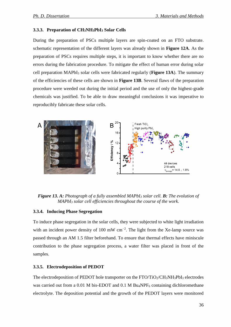
Ph. D. Dissertation 3. Materials and Methods
36
3.3.3. Preparation of CH3NH3PbI3 Solar Cells
During the preparation of PSCs multiple layers are spin-coated on an FTO substrate.
schematic representation of the different layers was already shown in Figure 12A. As the
preparation of PSCs requires multiple steps, it is important to know whether there are no
errors during the fabrication procedure. To mitigate the effect of human error during solar
cell preparation MAPbI3 solar cells were fabricated regularly (Figure 13A). The summary
of the efficiencies of these cells are shown in Figure 13B. Several flaws of the preparation
procedure were weeded out during the initial period and the use of only the highest-grade
chemicals was justified. To be able to draw meaningful conclusions it was imperative to
reproducibly fabricate these solar cells.
Figure 13. A: Photograph of a fully assembled MAPbI3 solar cell. B: The evolution of
MAPbI3 solar cell efficiencies throughout the course of the work.
3.3.4. Inducing Phase Segregation
To induce phase segregation in the solar cells, they were subjected to white light irradiation
with an incident power density of 100 mW cm−2. The light from the Xe-lamp source was
passed through an AM 1.5 filter beforehand. To ensure that thermal effects have miniscule
contribution to the phase segregation process, a water filter was placed in front of the
samples.
3.3.5. Electrodeposition of PEDOT
The electrodeposition of PEDOT hole transporter on the FTO/TiO2/CH3NH3PbI3 electrodes
was carried out from a 0.01 M bis-EDOT and 0.1 M Bu4NPF6 containing dichloromethane
electrolyte. The deposition potential and the growth of the PEDOT layers were monitored
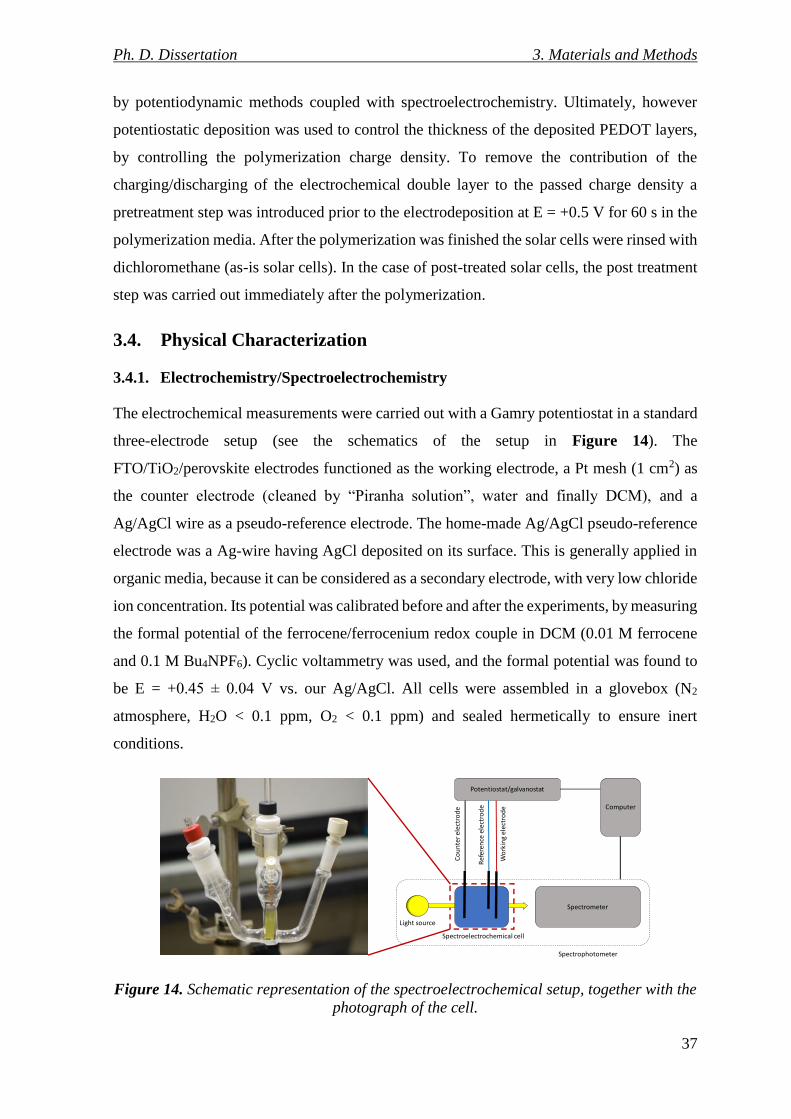
Ph. D. Dissertation 3. Materials and Methods
37
by potentiodynamic methods coupled with spectroelectrochemistry. Ultimately, however
potentiostatic deposition was used to control the thickness of the deposited PEDOT layers,
by controlling the polymerization charge density. To remove the contribution of the
charging/discharging of the electrochemical double layer to the passed charge density a
pretreatment step was introduced prior to the electrodeposition at E = +0.5 V for 60 s in the
polymerization media. After the polymerization was finished the solar cells were rinsed with
dichloromethane (as-is solar cells). In the case of post-treated solar cells, the post treatment
step was carried out immediately after the polymerization.
3.4. Physical Characterization
3.4.1. Electrochemistry/Spectroelectrochemistry
The electrochemical measurements were carried out with a Gamry potentiostat in a standard
three-electrode setup (see the schematics of the setup in Figure 14). The
FTO/TiO2/perovskite electrodes functioned as the working electrode, a Pt mesh (1 cm2) as
the counter electrode (cleaned by “Piranha solution”, water and finally DCM), and a
Ag/AgCl wire as a pseudo-reference electrode. The home-made Ag/AgCl pseudo-reference
electrode was a Ag-wire having AgCl deposited on its surface. This is generally applied in
organic media, because it can be considered as a secondary electrode, with very low chloride
ion concentration. Its potential was calibrated before and after the experiments, by measuring
the formal potential of the ferrocene/ferrocenium redox couple in DCM (0.01 M ferrocene
and 0.1 M Bu4NPF6). Cyclic voltammetry was used, and the formal potential was found to
be E = +0.45 ± 0.04 V vs. our Ag/AgCl. All cells were assembled in a glovebox (N2
atmosphere, H2O < 0.1 ppm, O2 < 0.1 ppm) and sealed hermetically to ensure inert
conditions.
Figure 14. Schematic representation of the spectroelectrochemical setup, together with the
photograph of the cell.
Spectrometer
Computer
Potentiostat/galvanostat
Light source
Spectroelectrochemical cell
Spectrophotometer
Wo
rkin
gel
ectr
od
e
Co
un
ter
elec
tro
de
Ref
eren
ceel
ectr
od
e
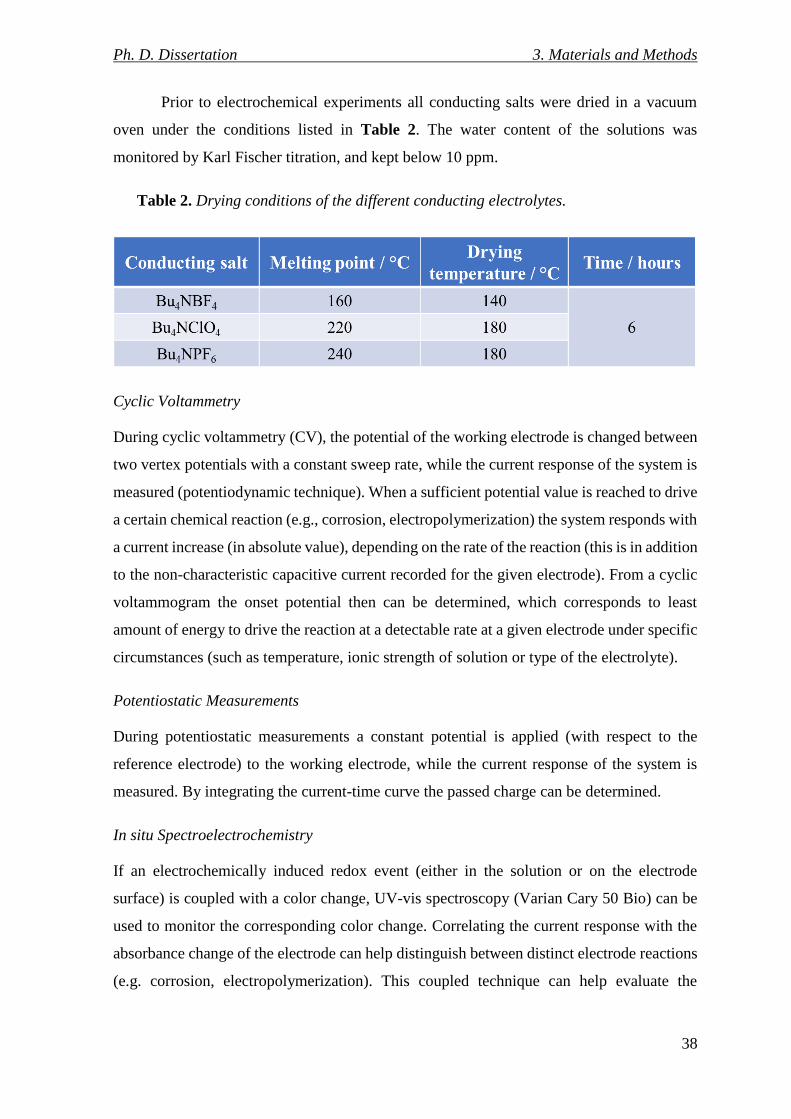
Ph. D. Dissertation 3. Materials and Methods
38
Prior to electrochemical experiments all conducting salts were dried in a vacuum
oven under the conditions listed in Table 2. The water content of the solutions was
monitored by Karl Fischer titration, and kept below 10 ppm.
Table 2. Drying conditions of the different conducting electrolytes.
Cyclic Voltammetry
During cyclic voltammetry (CV), the potential of the working electrode is changed between
two vertex potentials with a constant sweep rate, while the current response of the system is
measured (potentiodynamic technique). When a sufficient potential value is reached to drive
a certain chemical reaction (e.g., corrosion, electropolymerization) the system responds with
a current increase (in absolute value), depending on the rate of the reaction (this is in addition
to the non-characteristic capacitive current recorded for the given electrode). From a cyclic
voltammogram the onset potential then can be determined, which corresponds to least
amount of energy to drive the reaction at a detectable rate at a given electrode under specific
circumstances (such as temperature, ionic strength of solution or type of the electrolyte).
Potentiostatic Measurements
During potentiostatic measurements a constant potential is applied (with respect to the
reference electrode) to the working electrode, while the current response of the system is
measured. By integrating the current-time curve the passed charge can be determined.
In situ Spectroelectrochemistry
If an electrochemically induced redox event (either in the solution or on the electrode
surface) is coupled with a color change, UV-vis spectroscopy (Varian Cary 50 Bio) can be
used to monitor the corresponding color change. Correlating the current response with the
absorbance change of the electrode can help distinguish between distinct electrode reactions
(e.g. corrosion, electropolymerization). This coupled technique can help evaluate the
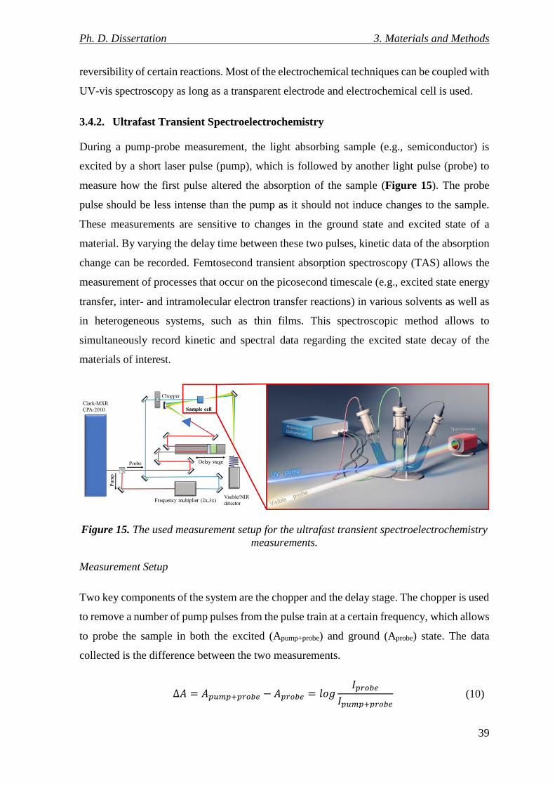
Ph. D. Dissertation 3. Materials and Methods
39
reversibility of certain reactions. Most of the electrochemical techniques can be coupled with
UV-vis spectroscopy as long as a transparent electrode and electrochemical cell is used.
3.4.2. Ultrafast Transient Spectroelectrochemistry
During a pump-probe measurement, the light absorbing sample (e.g., semiconductor) is
excited by a short laser pulse (pump), which is followed by another light pulse (probe) to
measure how the first pulse altered the absorption of the sample (Figure 15). The probe
pulse should be less intense than the pump as it should not induce changes to the sample.
These measurements are sensitive to changes in the ground state and excited state of a
material. By varying the delay time between these two pulses, kinetic data of the absorption
change can be recorded. Femtosecond transient absorption spectroscopy (TAS) allows the
measurement of processes that occur on the picosecond timescale (e.g., excited state energy
transfer, inter- and intramolecular electron transfer reactions) in various solvents as well as
in heterogeneous systems, such as thin films. This spectroscopic method allows to
simultaneously record kinetic and spectral data regarding the excited state decay of the
materials of interest.
Figure 15. The used measurement setup for the ultrafast transient spectroelectrochemistry
measurements.
Measurement Setup
Two key components of the system are the chopper and the delay stage. The chopper is used
to remove a number of pump pulses from the pulse train at a certain frequency, which allows
to probe the sample in both the excited (Apump+probe) and ground (Aprobe) state. The data
collected is the difference between the two measurements.
∆𝐴 = 𝐴𝑝𝑢𝑚𝑝+𝑝𝑟𝑜𝑏𝑒 − 𝐴𝑝𝑟𝑜𝑏𝑒 = 𝑙𝑜𝑔𝐼𝑝𝑟𝑜𝑏𝑒
𝐼𝑝𝑢𝑚𝑝+𝑝𝑟𝑜𝑏𝑒 (10)
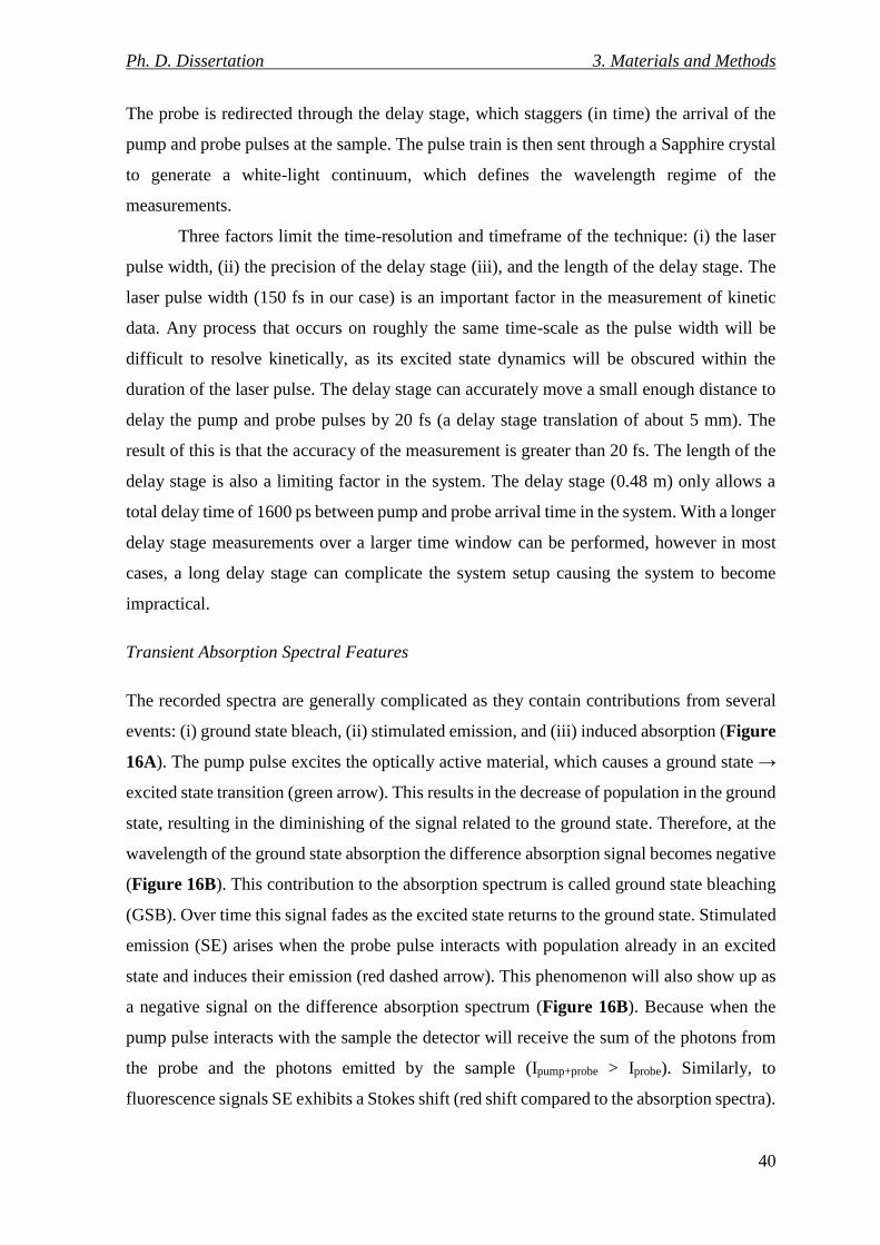
Ph. D. Dissertation 3. Materials and Methods
40
The probe is redirected through the delay stage, which staggers (in time) the arrival of the
pump and probe pulses at the sample. The pulse train is then sent through a Sapphire crystal
to generate a white-light continuum, which defines the wavelength regime of the
measurements.
Three factors limit the time-resolution and timeframe of the technique: (i) the laser
pulse width, (ii) the precision of the delay stage (iii), and the length of the delay stage. The
laser pulse width (150 fs in our case) is an important factor in the measurement of kinetic
data. Any process that occurs on roughly the same time-scale as the pulse width will be
difficult to resolve kinetically, as its excited state dynamics will be obscured within the
duration of the laser pulse. The delay stage can accurately move a small enough distance to
delay the pump and probe pulses by 20 fs (a delay stage translation of about 5 mm). The
result of this is that the accuracy of the measurement is greater than 20 fs. The length of the
delay stage is also a limiting factor in the system. The delay stage (0.48 m) only allows a
total delay time of 1600 ps between pump and probe arrival time in the system. With a longer
delay stage measurements over a larger time window can be performed, however in most
cases, a long delay stage can complicate the system setup causing the system to become
impractical.
Transient Absorption Spectral Features
The recorded spectra are generally complicated as they contain contributions from several
events: (i) ground state bleach, (ii) stimulated emission, and (iii) induced absorption (Figure
16A). The pump pulse excites the optically active material, which causes a ground state →
excited state transition (green arrow). This results in the decrease of population in the ground
state, resulting in the diminishing of the signal related to the ground state. Therefore, at the
wavelength of the ground state absorption the difference absorption signal becomes negative
(Figure 16B). This contribution to the absorption spectrum is called ground state bleaching
(GSB). Over time this signal fades as the excited state returns to the ground state. Stimulated
emission (SE) arises when the probe pulse interacts with population already in an excited
state and induces their emission (red dashed arrow). This phenomenon will also show up as
a negative signal on the difference absorption spectrum (Figure 16B). Because when the
pump pulse interacts with the sample the detector will receive the sum of the photons from
the probe and the photons emitted by the sample (Ipump+probe > Iprobe). Similarly, to
fluorescence signals SE exhibits a Stokes shift (red shift compared to the absorption spectra).
Ph. D. Dissertation 3. Materials and Methods
41
Induced absorption (IA) is the result of the excited state absorbing another photon and thus
occupying an even higher excited state (blue dotted line). This can only occur in the excited
state, thus it appears as a positive signal on the difference absorption spectra (Figure 16B).
Figure 16. A: Energy levels of a hypothetical optically active sample and some quantum
transitions influencing the difference absorption spectrum. B: The corresponding
difference absorption spectrum with the separate contributions of the different transitions.
Ultrafast-spectroelectrochemistry
TAS measurements are usually conducted on thin film samples or solutions placed in a
cuvette. However, by replacing the cuvette with an electrochemical cell, and using
transparent electrodes, the measurement can be coupled with electrochemical techniques.
A Clark MXR-2010 laser system (775 nm fundamental, 1 mJ/pulse, FWHM=150 fs,
1 kHz repetition rate) was used to perform the ultrafast transient spectroelectrochemistry
measurements. The data was collected using a Helios software from Ultrafast Systems. The
fundamental was separated in an intensity ratio of 95/5, where the 95% was doubled in
frequency to generate the 387 nm excitation pump. The remaining 5% was used to generate
a white light continuum via a CaF2 crystal. This light was used as the probe for all
measurements. The intensity of the excitation pump was modulated so that the maximum
change in absorbance remained constant in all measurements (A520nm ~ −0.25), which
corresponded to a pump excitation of about 12 μJ cm−2. This was done to ensure that similar
amounts of charge carriers were generated in each measurement. A three-armed
electrochemical cell with a fused silica cuvette body was placed at the spatial overlap of the
pump and the probe. The electrode was kept at a constant potential while the TA spectra
Ph. D. Dissertation 3. Materials and Methods
42
were recorded. The sampling spot was adjusted between every measurement to ensure the
sampling of a fresh electrode area.
3.4.3. X-ray Photoelectron Spectroscopy
To gain information on the surface composition and the distinct chemical states of elements
on the electrode surface X-ray photoelectron spectroscopy (XPS) was used. XPS is a highly
surface sensitive technique, thus the information is acquired from the upper 1-10 nm region
of the sample.
The XP spectra were recorded with a PHI VersaProbe II system. The binding energy
scale was corrected by fixing the main C 1s component to 284.8 eV, corresponding to the
adventitious carbon. For spectrum acquisition and evaluation, the MultiPak software was
used. To fit the XP spectra and determine the elemental composition of the different samples
a Shirley background was used. First the spectra of the pure CsPbBr3 samples were fitted.
From these fittings the profile shape, position and FWHM of the fitting functions were
determined. For the electrochemically treated samples these fittings functioned as starting
parameters, from which the shape and FWHM was held constant for each subsequent fitting.
Small variation in the peak position was allowed for each fit. If the fitting was inadequate,
another component was added to the process.
3.4.4. Scanning Electron Microscopy
Top-down and cross-sectional scanning electron microscopic (SEM) images were captured
using a FEI Helios NanoLab™ DualBeam™ instrument. Elemental composition of the
samples was analysed by energy dispersive X-ray spectroscopy (EDX).
3.4.5. X-ray Diffraction
X-ray diffraction (XRD) patterns were collected using a Bruker D8 DISCOVER instrument
with Cu K X-ray source ( = 1.5406 Å), in the 20−80 ° range, with a 2 ° min−1 scan rate.
3.4.6. Raman-spectroscopy
Raman spectroscopic measurements were performed on a DXR Raman Microscope using a
green laser (= 532 nm), operating at 10 mW laser power at room temperature.
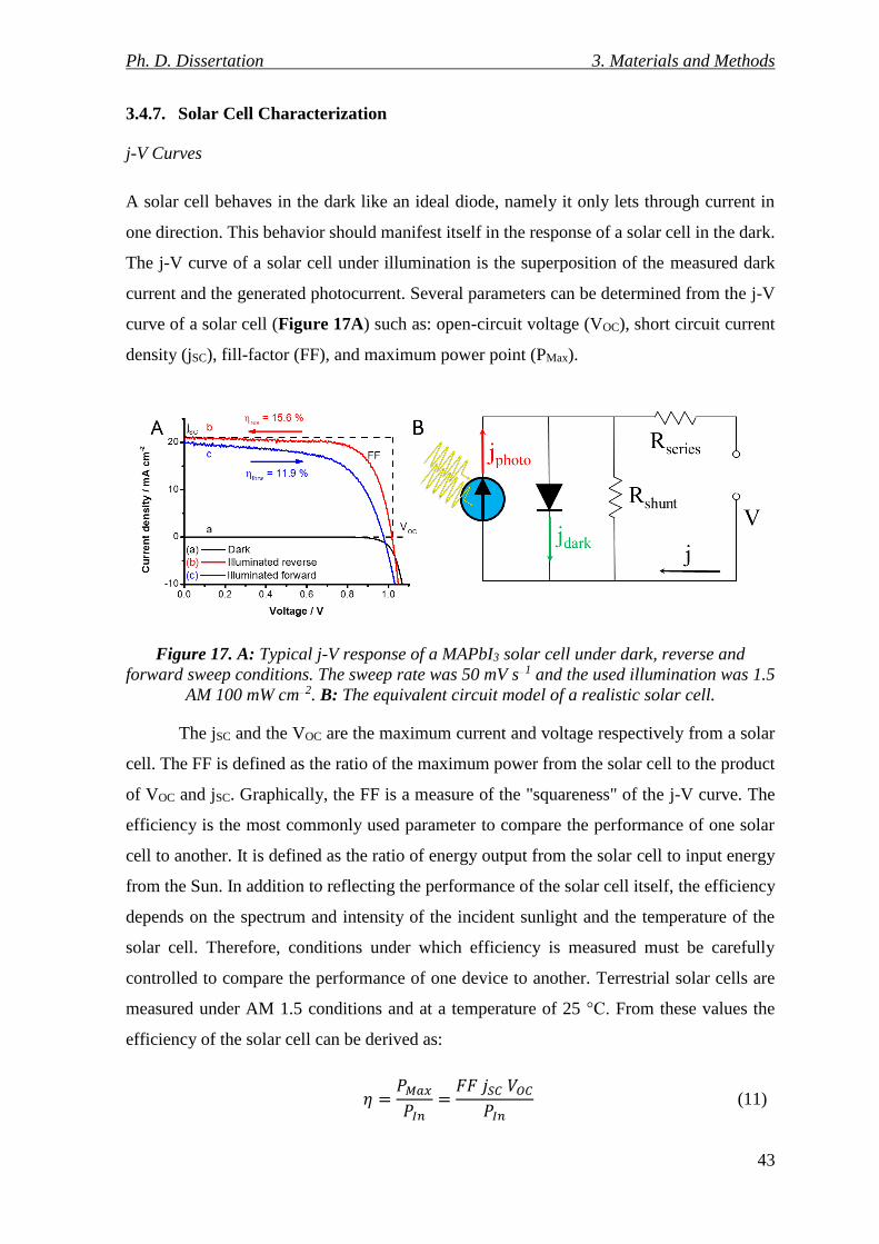
Ph. D. Dissertation 3. Materials and Methods
43
3.4.7. Solar Cell Characterization
j-V Curves
A solar cell behaves in the dark like an ideal diode, namely it only lets through current in
one direction. This behavior should manifest itself in the response of a solar cell in the dark.
The j-V curve of a solar cell under illumination is the superposition of the measured dark
current and the generated photocurrent. Several parameters can be determined from the j-V
curve of a solar cell (Figure 17A) such as: open-circuit voltage (VOC), short circuit current
density (jSC), fill-factor (FF), and maximum power point (PMax).
Figure 17. A: Typical j-V response of a MAPbI3 solar cell under dark, reverse and
forward sweep conditions. The sweep rate was 50 mV s−1 and the used illumination was 1.5
AM 100 mW cm−2. B: The equivalent circuit model of a realistic solar cell.
The jSC and the VOC are the maximum current and voltage respectively from a solar
cell. The FF is defined as the ratio of the maximum power from the solar cell to the product
of VOC and jSC. Graphically, the FF is a measure of the "squareness" of the j-V curve. The
efficiency is the most commonly used parameter to compare the performance of one solar
cell to another. It is defined as the ratio of energy output from the solar cell to input energy
from the Sun. In addition to reflecting the performance of the solar cell itself, the efficiency
depends on the spectrum and intensity of the incident sunlight and the temperature of the
solar cell. Therefore, conditions under which efficiency is measured must be carefully
controlled to compare the performance of one device to another. Terrestrial solar cells are
measured under AM 1.5 conditions and at a temperature of 25 °C. From these values the
efficiency of the solar cell can be derived as:
𝜂 =𝑃𝑀𝑎𝑥𝑃𝐼𝑛
=𝐹𝐹 𝑗𝑆𝐶 𝑉𝑂𝐶𝑃𝐼𝑛
(11)
Ph. D. Dissertation 3. Materials and Methods
44
The shape of a j-V curve can be indicative of parasitic losses in the cell. These
resistive losses can severely distort the shape of the j-V curve. These can be integrated into
the equivalent circuit model of the solar cell (Figure 17B). One of the losses acts as a series
resistance (RSeries). Three causes for this behavior can be identified: (i) current passing
through the emitter and base of the solar cell, (ii) contact resistance between the metal contact
and the solar cell, and (iii) resistance of the top and rear metal contacts. The main impact of
RSeries is to reduce the FF, although excessively high values may also reduce the jSC as well.
Significant power losses caused by the presence of a shunt resistance (RShunt), which is
typically caused by defects in the material (recombination), rather than poor solar cell design.
Low RShunt causes power losses in solar cells by providing an alternate current path for the
light-generated current. Such a diversion reduces the amount of current flowing through the
solar cell junction and reduces the voltage from the solar cell.
The characterization of the solar cells was performed in a 2-electrode setup on a
Princeton Applied Research PARStat 2273 potentiostat under 1 sun conditions. The voltage
was swept with a 50 mV s−1 sweep rate.
IPCE measurement
During an incident photon to charge carrier conversion efficiency (IPCE) measurement the
current response of the solar cell is recorded in the function of the wavelength of the incident
light (technically external quantum efficiency measurement). IPCE measures how efficiently
the solar cell converts photons to charge carriers. Two types of quantum efficiencies can be
distinguished: external and internal. The difference is that internal quantum efficiency only
considers photons that are absorbed by the material and excludes photons that are reflected
or transmitted at a given wavelength.
The IPCE curve can be used to determine the overall current response of a device to
a given light source with known spectral distribution. By using the spectral distribution of
solar light (AM 1.5 100 mW cm−2) this should be equal to the jSC value determined from a
j-V curve (if the j-V sweep represents the true performance characteristics of the device). A
certain degree of discrepancy between the two measurements can be expected considering
that IPCE measurements are carried out at a single wavelength with much lower intensity
than one sun irradiation.[202] IPCE measurements were taken with a Newport Oriel Quantum
Efficiency Measurement System.
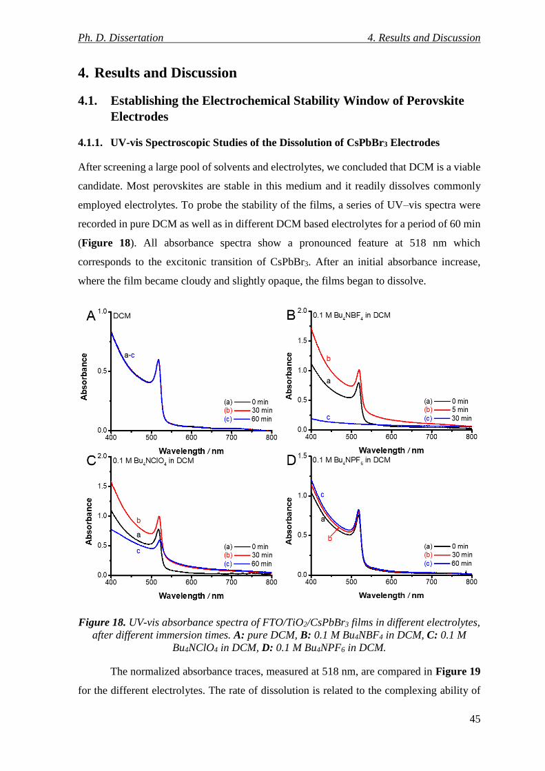
Ph. D. Dissertation 4. Results and Discussion
45
4. Results and Discussion
4.1. Establishing the Electrochemical Stability Window of Perovskite
Electrodes
4.1.1. UV-vis Spectroscopic Studies of the Dissolution of CsPbBr3 Electrodes
After screening a large pool of solvents and electrolytes, we concluded that DCM is a viable
candidate. Most perovskites are stable in this medium and it readily dissolves commonly
employed electrolytes. To probe the stability of the films, a series of UV–vis spectra were
recorded in pure DCM as well as in different DCM based electrolytes for a period of 60 min
(Figure 18). All absorbance spectra show a pronounced feature at 518 nm which
corresponds to the excitonic transition of CsPbBr3. After an initial absorbance increase,
where the film became cloudy and slightly opaque, the films began to dissolve.
Figure 18. UV-vis absorbance spectra of FTO/TiO2/CsPbBr3 films in different electrolytes,
after different immersion times. A: pure DCM, B: 0.1 M Bu4NBF4 in DCM, C: 0.1 M
Bu4NClO4 in DCM, D: 0.1 M Bu4NPF6 in DCM.
The normalized absorbance traces, measured at 518 nm, are compared in Figure 19
for the different electrolytes. The rate of dissolution is related to the complexing ability of
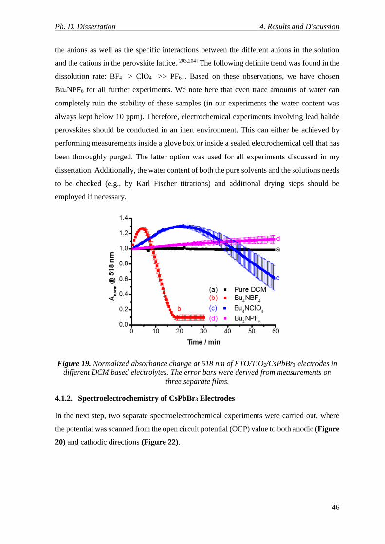
Ph. D. Dissertation 4. Results and Discussion
46
the anions as well as the specific interactions between the different anions in the solution
and the cations in the perovskite lattice.[203,204] The following definite trend was found in the
dissolution rate: BF4− > ClO4
− >> PF6−. Based on these observations, we have chosen
Bu4NPF6 for all further experiments. We note here that even trace amounts of water can
completely ruin the stability of these samples (in our experiments the water content was
always kept below 10 ppm). Therefore, electrochemical experiments involving lead halide
perovskites should be conducted in an inert environment. This can either be achieved by
performing measurements inside a glove box or inside a sealed electrochemical cell that has
been thoroughly purged. The latter option was used for all experiments discussed in my
dissertation. Additionally, the water content of both the pure solvents and the solutions needs
to be checked (e.g., by Karl Fischer titrations) and additional drying steps should be
employed if necessary.
Figure 19. Normalized absorbance change at 518 nm of FTO/TiO2/CsPbBr3 electrodes in
different DCM based electrolytes. The error bars were derived from measurements on
three separate films.
4.1.2. Spectroelectrochemistry of CsPbBr3 Electrodes
In the next step, two separate spectroelectrochemical experiments were carried out, where
the potential was scanned from the open circuit potential (OCP) value to both anodic (Figure
20) and cathodic directions (Figure 22).
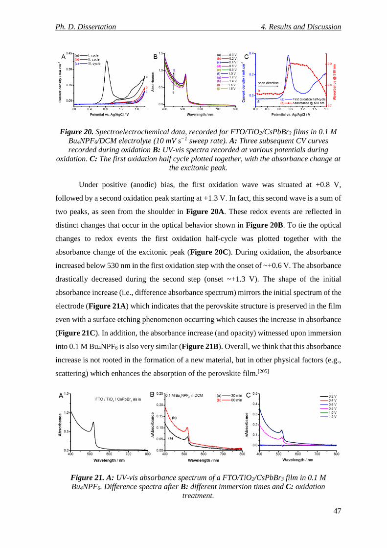
Ph. D. Dissertation 4. Results and Discussion
47
Figure 20. Spectroelectrochemical data, recorded for FTO/TiO2/CsPbBr3 films in 0.1 M
Bu4NPF6/DCM electrolyte (10 mV s−1 sweep rate). A: Three subsequent CV curves
recorded during oxidation B: UV-vis spectra recorded at various potentials during
oxidation. C: The first oxidation half cycle plotted together, with the absorbance change at
the excitonic peak.
Under positive (anodic) bias, the first oxidation wave was situated at +0.8 V,
followed by a second oxidation peak starting at +1.3 V. In fact, this second wave is a sum of
two peaks, as seen from the shoulder in Figure 20A. These redox events are reflected in
distinct changes that occur in the optical behavior shown in Figure 20B. To tie the optical
changes to redox events the first oxidation half-cycle was plotted together with the
absorbance change of the excitonic peak (Figure 20C). During oxidation, the absorbance
increased below 530 nm in the first oxidation step with the onset of ~+0.6 V. The absorbance
drastically decreased during the second step (onset ~+1.3 V). The shape of the initial
absorbance increase (i.e., difference absorbance spectrum) mirrors the initial spectrum of the
electrode (Figure 21A) which indicates that the perovskite structure is preserved in the film
even with a surface etching phenomenon occurring which causes the increase in absorbance
(Figure 21C). In addition, the absorbance increase (and opacity) witnessed upon immersion
into 0.1 M Bu4NPF6 is also very similar (Figure 21B). Overall, we think that this absorbance
increase is not rooted in the formation of a new material, but in other physical factors (e.g.,
scattering) which enhances the absorption of the perovskite film.[205]
Figure 21. A: UV-vis absorbance spectrum of a FTO/TiO2/CsPbBr3 film in 0.1 M
Bu4NPF6. Difference spectra after B: different immersion times and C: oxidation
treatment.
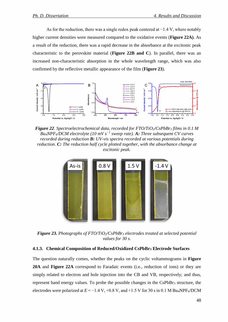
Ph. D. Dissertation 4. Results and Discussion
48
As for the reduction, there was a single redox peak centered at −1.4 V, where notably
higher current densities were measured compared to the oxidative events (Figure 22A). As
a result of the reduction, there was a rapid decrease in the absorbance at the excitonic peak
characteristic to the perovskite material (Figure 22B and C). In parallel, there was an
increased non-characteristic absorption in the whole wavelength range, which was also
confirmed by the reflective metallic appearance of the film (Figure 23).
Figure 22. Spectroelectrochemical data, recorded for FTO/TiO2/CsPbBr3 films in 0.1 M
Bu4NPF6/DCM electrolyte (10 mV s−1 sweep rate). A: Three subsequent CV curves
recorded during reduction B: UV-vis spectra recorded at various potentials during
reduction. C: The reduction half cycle plotted together, with the absorbance change at
excitonic peak.
Figure 23. Photographs of FTO/TiO2/CsPbBr3 electrodes treated at selected potential
values for 30 s.
4.1.3. Chemical Composition of Reduced/Oxidized CsPbBr3 Electrode Surfaces
The question naturally comes, whether the peaks on the cyclic voltammograms in Figure
20A and Figure 22A correspond to Faradaic events (i.e., reduction of ions) or they are
simply related to electron and hole injection into the CB and VB, respectively; and thus,
represent band energy values. To probe the possible changes in the CsPbBr3 structure, the
electrodes were polarized at E = −1.4 V, +0.8 V, and +1.5 V for 30 s in 0.1 M Bu4NPF6/DCM
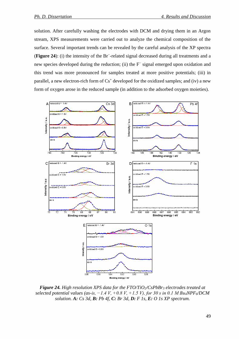
Ph. D. Dissertation 4. Results and Discussion
49
solution. After carefully washing the electrodes with DCM and drying them in an Argon
stream, XPS measurements were carried out to analyze the chemical composition of the
surface. Several important trends can be revealed by the careful analysis of the XP spectra
(Figure 24): (i) the intensity of the Br−-related signal decreased during all treatments and a
new species developed during the reduction; (ii) the F− signal emerged upon oxidation and
this trend was more pronounced for samples treated at more positive potentials; (iii) in
parallel, a new electron-rich form of Cs+ developed for the oxidized samples; and (iv) a new
form of oxygen arose in the reduced sample (in addition to the adsorbed oxygen moieties).
Figure 24. High resolution XPS data for the FTO/TiO2/CsPbBr3 electrodes treated at
selected potential values (as-is, −1.4 V, +0.8 V, +1.5 V), for 30 s in 0.1 M Bu4NPF6/DCM
solution. A: Cs 3d, B: Pb 4f, C: Br 3d, D: F 1s, E: O 1s XP spectrum.
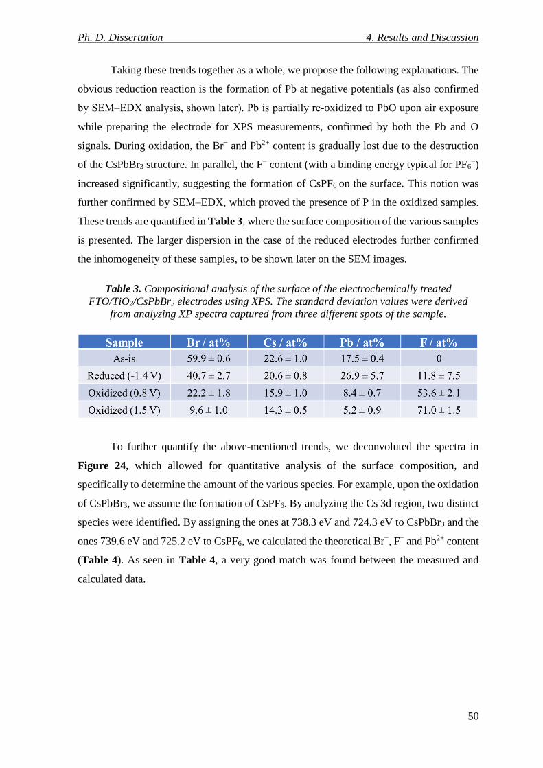
Ph. D. Dissertation 4. Results and Discussion
50
Taking these trends together as a whole, we propose the following explanations. The
obvious reduction reaction is the formation of Pb at negative potentials (as also confirmed
by SEM‒EDX analysis, shown later). Pb is partially re-oxidized to PbO upon air exposure
while preparing the electrode for XPS measurements, confirmed by both the Pb and O
signals. During oxidation, the Br− and Pb2+ content is gradually lost due to the destruction
of the CsPbBr3 structure. In parallel, the F− content (with a binding energy typical for PF6−)
increased significantly, suggesting the formation of CsPF6 on the surface. This notion was
further confirmed by SEM–EDX, which proved the presence of P in the oxidized samples.
These trends are quantified in Table 3, where the surface composition of the various samples
is presented. The larger dispersion in the case of the reduced electrodes further confirmed
the inhomogeneity of these samples, to be shown later on the SEM images.
Table 3. Compositional analysis of the surface of the electrochemically treated
FTO/TiO2/CsPbBr3 electrodes using XPS. The standard deviation values were derived
from analyzing XP spectra captured from three different spots of the sample.
To further quantify the above-mentioned trends, we deconvoluted the spectra in
Figure 24, which allowed for quantitative analysis of the surface composition, and
specifically to determine the amount of the various species. For example, upon the oxidation
of CsPbBr3, we assume the formation of CsPF6. By analyzing the Cs 3d region, two distinct
species were identified. By assigning the ones at 738.3 eV and 724.3 eV to CsPbBr3 and the
ones 739.6 eV and 725.2 eV to CsPF6, we calculated the theoretical Br−, F− and Pb2+ content
(Table 4). As seen in Table 4, a very good match was found between the measured and
calculated data.
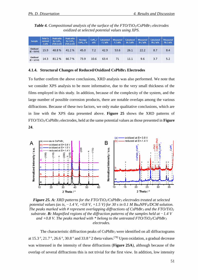
Ph. D. Dissertation 4. Results and Discussion
51
Table 4. Compositional analysis of the surface of the FTO/TiO2/CsPbBr3 electrodes
oxidized at selected potential values using XPS.
4.1.4. Structural Changes of Reduced/Oxidized CsPbBr3 Electrodes
To further confirm the above conclusions, XRD analysis was also performed. We note that
we consider XPS analysis to be more informative, due to the very small thickness of the
films employed in this study. In addition, because of the complexity of the system, and the
large number of possible corrosion products, there are notable overlaps among the various
diffractions. Because of these two factors, we only make qualitative conclusions, which are
in line with the XPS data presented above. Figure 25 shows the XRD patterns of
FTO/TiO2/CsPbBr3 electrodes, held at the same potential values as those presented in Figure
24.
Figure 25. A: XRD patterns for the FTO/TiO2/CsPbBr3 electrodes treated at selected
potential values (as is, −1.4 V, +0.8 V, +1.5 V) for 30 s in 0.1 M Bu4NPF6/DCM solution.
The peaks marked with # represent overlapping diffractions of CsPbBr3 and the FTO/TiO2
substrate. B: Magnified regions of the diffraction patterns of the samples held at −1.4 V
and +0.8 V. The peaks marked with * belong to the untreated FTO/TiO2/CsPbBr3
electrodes.
The characteristic diffraction peaks of CsPbBr3 were identified on all diffractograms
at 15.3 o, 21.7 o, 26.6 o, 30.8 o and 33.8 o 2 theta values.[78] Upon oxidation, a gradual decrease
was witnessed in the intensity of these diffractions (Figure 25A), although because of the
overlap of several diffractions this is not trivial for the first view. In addition, low intensity
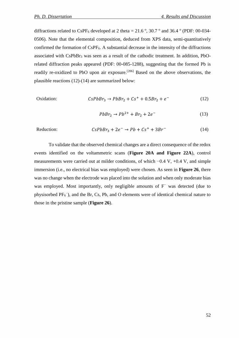
Ph. D. Dissertation 4. Results and Discussion
52
diffractions related to CsPF6 developed at 2 theta = 21.6 o, 30.7 o and 36.4 o (PDF: 00-034-
0506). Note that the elemental composition, deduced from XPS data, semi-quantitatively
confirmed the formation of CsPF6. A substantial decrease in the intensity of the diffractions
associated with CsPbBr3 was seen as a result of the cathodic treatment. In addition, PbO-
related diffraction peaks appeared (PDF: 00-085-1288), suggesting that the formed Pb is
readily re-oxidized to PbO upon air exposure.[206] Based on the above observations, the
plausible reactions (12)-(14) are summarized below:
Oxidation: 𝐶𝑠𝑃𝑏𝐵𝑟3 → 𝑃𝑏𝐵𝑟2 + 𝐶𝑠+ + 0.5𝐵𝑟2 + 𝑒
− (12)
𝑃𝑏𝐵𝑟2 → 𝑃𝑏2+ + 𝐵𝑟2 + 2𝑒
− (13)
Reduction: 𝐶𝑠𝑃𝑏𝐵𝑟3 + 2𝑒− → 𝑃𝑏 + 𝐶𝑠+ + 3𝐵𝑟− (14)
To validate that the observed chemical changes are a direct consequence of the redox
events identified on the voltammetric scans (Figure 20A and Figure 22A), control
measurements were carried out at milder conditions, of which −0.4 V, +0.4 V, and simple
immersion (i.e., no electrical bias was employed) were chosen. As seen in Figure 26, there
was no change when the electrode was placed into the solution and when only moderate bias
was employed. Most importantly, only negligible amounts of F− was detected (due to
physisorbed PF6−), and the Br, Cs, Pb, and O elements were of identical chemical nature to
those in the pristine sample (Figure 26).
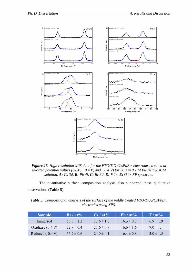
Ph. D. Dissertation 4. Results and Discussion
53
Figure 26. High resolution XPS data for the FTO/TiO2/CsPbBr3 electrodes, treated at
selected potential values (OCP, −0.4 V, and +0.4 V) for 30 s in 0.1 M Bu4NPF6/DCM
solution. A: Cs 3d, B: Pb 4f, C: Br 3d, D: F 1s, E: O 1s XP spectrum.
The quantitative surface composition analysis also supported these qualitative
observations (Table 5).
Table 5. Compositional analysis of the surface of the mildly treated FTO/TiO2/CsPbBr3
electrodes using XPS.
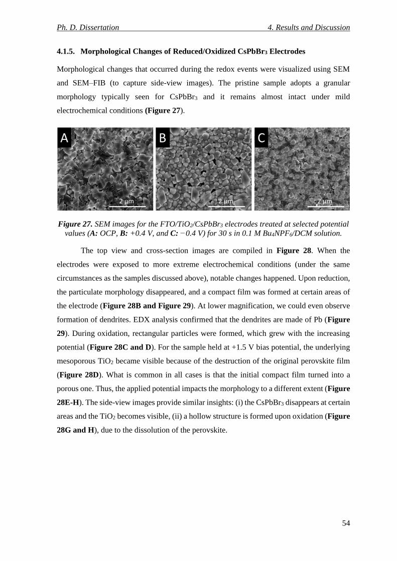
Ph. D. Dissertation 4. Results and Discussion
54
4.1.5. Morphological Changes of Reduced/Oxidized CsPbBr3 Electrodes
Morphological changes that occurred during the redox events were visualized using SEM
and SEM–FIB (to capture side-view images). The pristine sample adopts a granular
morphology typically seen for CsPbBr3 and it remains almost intact under mild
electrochemical conditions (Figure 27).
Figure 27. SEM images for the FTO/TiO2/CsPbBr3 electrodes treated at selected potential
values (A: OCP, B: +0.4 V, and C: −0.4 V) for 30 s in 0.1 M Bu4NPF6/DCM solution.
The top view and cross-section images are compiled in Figure 28. When the
electrodes were exposed to more extreme electrochemical conditions (under the same
circumstances as the samples discussed above), notable changes happened. Upon reduction,
the particulate morphology disappeared, and a compact film was formed at certain areas of
the electrode (Figure 28B and Figure 29). At lower magnification, we could even observe
formation of dendrites. EDX analysis confirmed that the dendrites are made of Pb (Figure
29). During oxidation, rectangular particles were formed, which grew with the increasing
potential (Figure 28C and D). For the sample held at +1.5 V bias potential, the underlying
mesoporous TiO2 became visible because of the destruction of the original perovskite film
(Figure 28D). What is common in all cases is that the initial compact film turned into a
porous one. Thus, the applied potential impacts the morphology to a different extent (Figure
28E-H). The side-view images provide similar insights: (i) the CsPbBr3 disappears at certain
areas and the TiO2 becomes visible, (ii) a hollow structure is formed upon oxidation (Figure
28G and H), due to the dissolution of the perovskite.
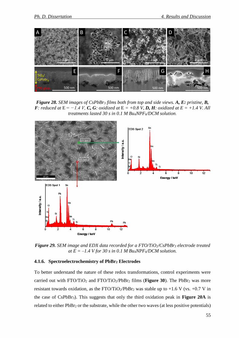
Ph. D. Dissertation 4. Results and Discussion
55
Figure 28. SEM images of CsPbBr3 films both from top and side views. A, E: pristine, B,
F: reduced at E = −1.4 V, C, G: oxidized at E = +0.8 V, D, H: oxidized at E = +1.4 V. All
treatments lasted 30 s in 0.1 M Bu4NPF6/DCM solution.
Figure 29. SEM image and EDX data recorded for a FTO/TiO2/CsPbBr3 electrode treated
at E = ‒1.4 V for 30 s in 0.1 M Bu4NPF6/DCM solution.
4.1.6. Spectroelectrochemistry of PbBr2 Electrodes
To better understand the nature of these redox transformations, control experiments were
carried out with FTO/TiO2 and FTO/TiO2/PbBr2 films (Figure 30). The PbBr2 was more
resistant towards oxidation, as the FTO/TiO2/PbBr2 was stable up to +1.6 V (vs. +0.7 V in
the case of CsPbBr3). This suggests that only the third oxidation peak in Figure 20A is
related to either PbBr2 or the substrate, while the other two waves (at less positive potentials)
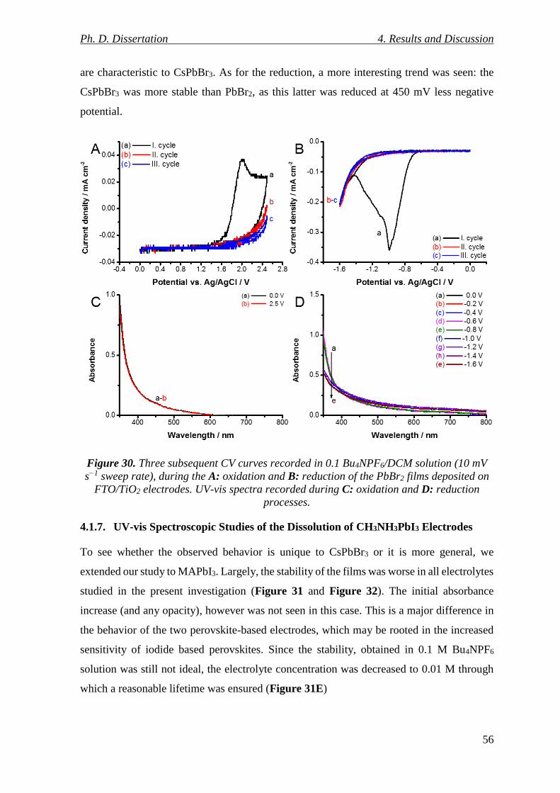
Ph. D. Dissertation 4. Results and Discussion
56
are characteristic to CsPbBr3. As for the reduction, a more interesting trend was seen: the
CsPbBr3 was more stable than PbBr2, as this latter was reduced at 450 mV less negative
potential.
Figure 30. Three subsequent CV curves recorded in 0.1 Bu4NPF6/DCM solution (10 mV
s−1 sweep rate), during the A: oxidation and B: reduction of the PbBr2 films deposited on
FTO/TiO2 electrodes. UV-vis spectra recorded during C: oxidation and D: reduction
processes.
4.1.7. UV-vis Spectroscopic Studies of the Dissolution of CH3NH3PbI3 Electrodes
To see whether the observed behavior is unique to CsPbBr3 or it is more general, we
extended our study to MAPbI3. Largely, the stability of the films was worse in all electrolytes
studied in the present investigation (Figure 31 and Figure 32). The initial absorbance
increase (and any opacity), however was not seen in this case. This is a major difference in
the behavior of the two perovskite-based electrodes, which may be rooted in the increased
sensitivity of iodide based perovskites. Since the stability, obtained in 0.1 M Bu4NPF6
solution was still not ideal, the electrolyte concentration was decreased to 0.01 M through
which a reasonable lifetime was ensured (Figure 31E)
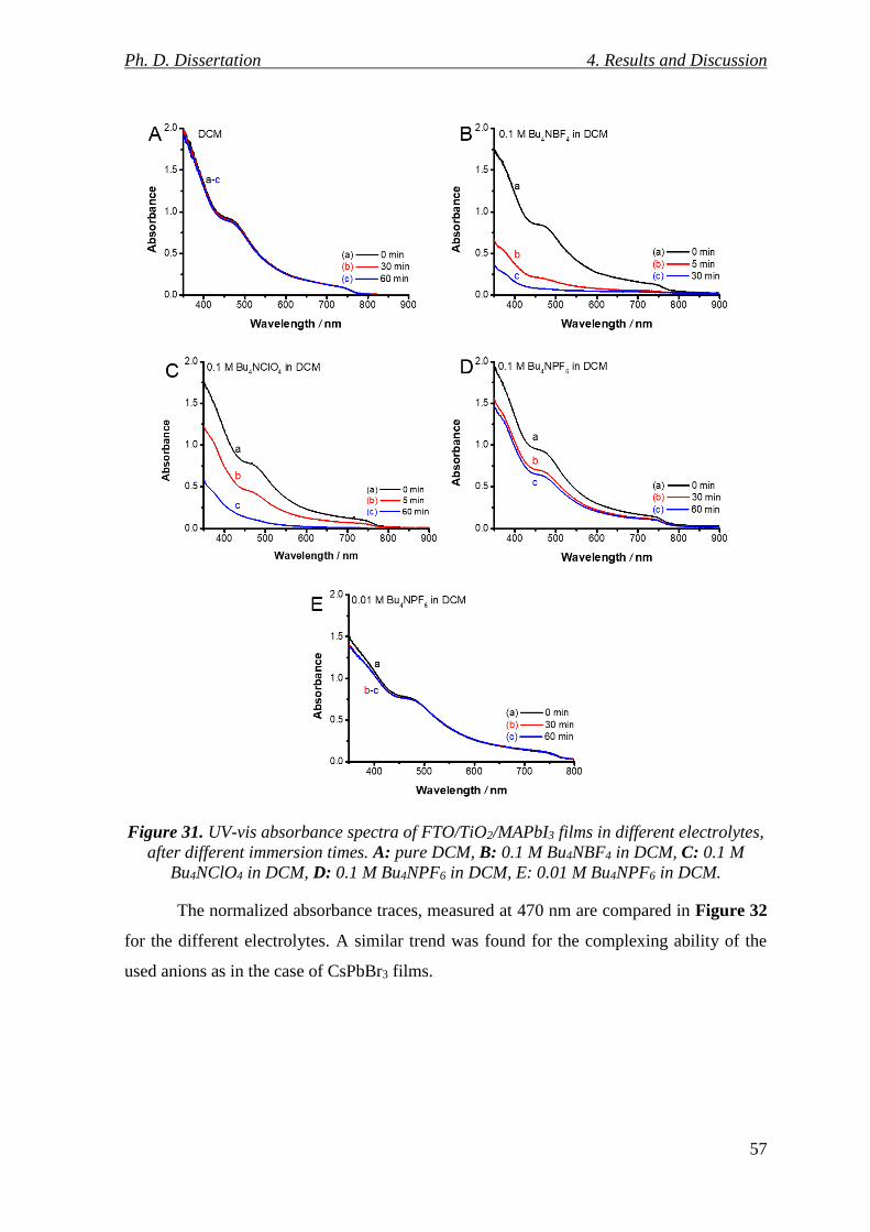
Ph. D. Dissertation 4. Results and Discussion
57
Figure 31. UV-vis absorbance spectra of FTO/TiO2/MAPbI3 films in different electrolytes,
after different immersion times. A: pure DCM, B: 0.1 M Bu4NBF4 in DCM, C: 0.1 M
Bu4NClO4 in DCM, D: 0.1 M Bu4NPF6 in DCM, E: 0.01 M Bu4NPF6 in DCM.
The normalized absorbance traces, measured at 470 nm are compared in Figure 32
for the different electrolytes. A similar trend was found for the complexing ability of the
used anions as in the case of CsPbBr3 films.
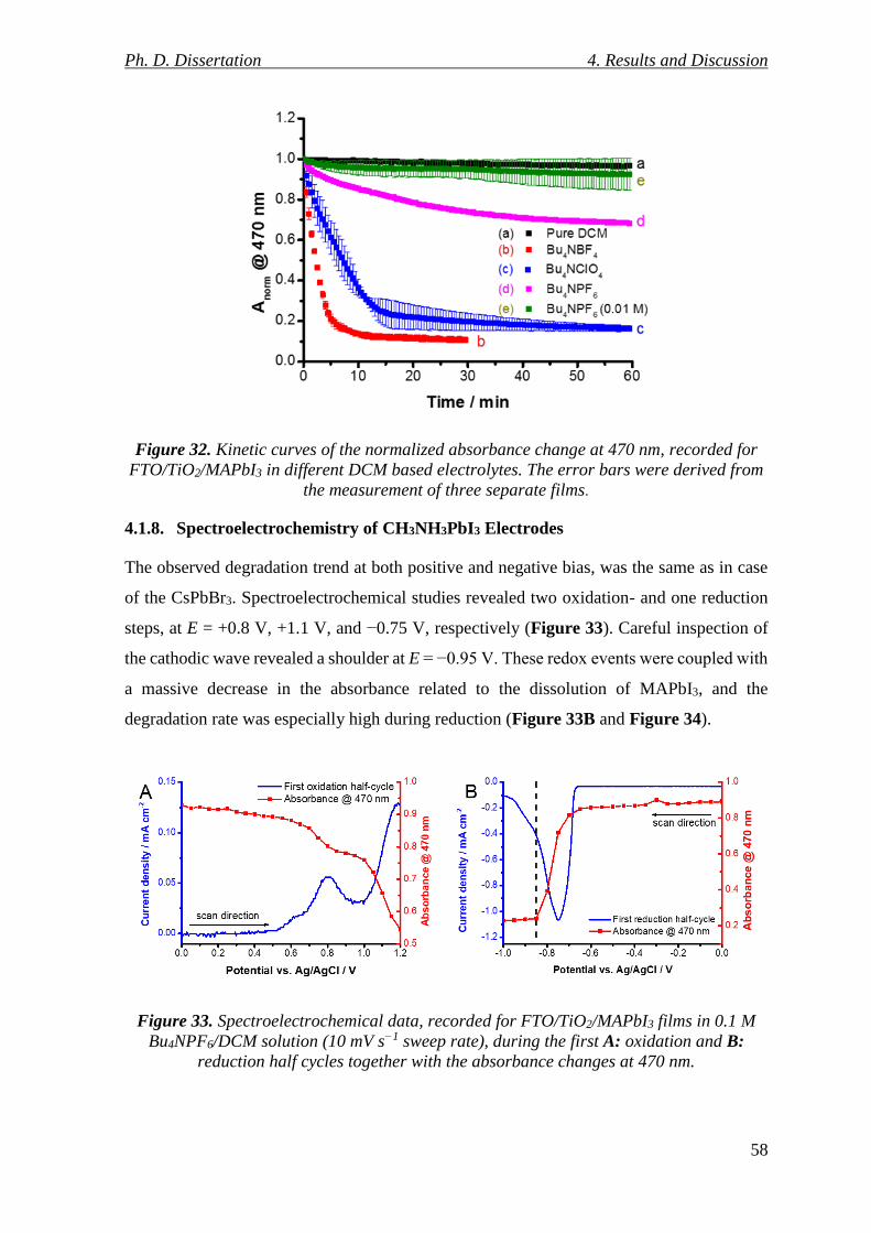
Ph. D. Dissertation 4. Results and Discussion
58
Figure 32. Kinetic curves of the normalized absorbance change at 470 nm, recorded for
FTO/TiO2/MAPbI3 in different DCM based electrolytes. The error bars were derived from
the measurement of three separate films.
4.1.8. Spectroelectrochemistry of CH3NH3PbI3 Electrodes
The observed degradation trend at both positive and negative bias, was the same as in case
of the CsPbBr3. Spectroelectrochemical studies revealed two oxidation- and one reduction
steps, at E = +0.8 V, +1.1 V, and −0.75 V, respectively (Figure 33). Careful inspection of
the cathodic wave revealed a shoulder at E = −0.95 V. These redox events were coupled with
a massive decrease in the absorbance related to the dissolution of MAPbI3, and the
degradation rate was especially high during reduction (Figure 33B and Figure 34).
Figure 33. Spectroelectrochemical data, recorded for FTO/TiO2/MAPbI3 films in 0.1 M
Bu4NPF6/DCM solution (10 mV s−1 sweep rate), during the first A: oxidation and B:
reduction half cycles together with the absorbance changes at 470 nm.
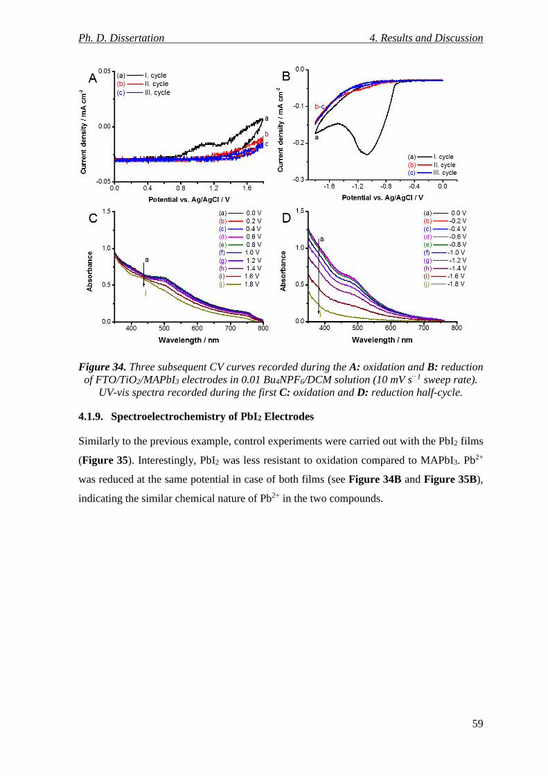
Ph. D. Dissertation 4. Results and Discussion
59
Figure 34. Three subsequent CV curves recorded during the A: oxidation and B: reduction
of FTO/TiO2/MAPbI3 electrodes in 0.01 Bu4NPF6/DCM solution (10 mV s−1 sweep rate).
UV-vis spectra recorded during the first C: oxidation and D: reduction half-cycle.
4.1.9. Spectroelectrochemistry of PbI2 Electrodes
Similarly to the previous example, control experiments were carried out with the PbI2 films
(Figure 35). Interestingly, PbI2 was less resistant to oxidation compared to MAPbI3. Pb2+
was reduced at the same potential in case of both films (see Figure 34B and Figure 35B),
indicating the similar chemical nature of Pb2+ in the two compounds.

Ph. D. Dissertation 4. Results and Discussion
60
Figure 35. Three subsequent CV curves recorded in 0.1 Bu4NPF6/DCM solution (10 mV
s−1 sweep rate), during the A: oxidation and B: reduction of the PbI2 films deposited on
FTO/TiO2 electrodes. UV-vis spectra recorded during the first C: oxidation and D:
reduction half-cycles.
4.1.10. Potential Diagram of Optically Active Perovskite Electrodes
Taking the above results together, we constructed a potential diagram (Figure 36) to
compare the potentials of the various redox events, deduced from the spectroelectrochemical
studies. The position of the redox events was always calculated from the onset potential of
the redox waves. The band edge positions of the perovskite materials were obtained from
previous literature data, and serve semi-quantitative comparison, because the film
preparation methods were not identical.[207,208] This representation, together with the
previously demonstrated structural analysis, allows to answer the initial question of whether
the currents measured during the voltammetric curves are related to charge carrier injection
into the materials and/or to real Faradaic events. As for CsPbBr3, a good match can be
revealed between the potential of the reduction peak and the CB edge; as well as the second
oxidation peak and the VB edge. More interestingly, the first oxidation event occurs at a less
positive potential than the VB, meaning that the CsPbBr3 is irreversibly oxidized before hole
injection could take place. Based on all the evidences gathered in this study, these potential
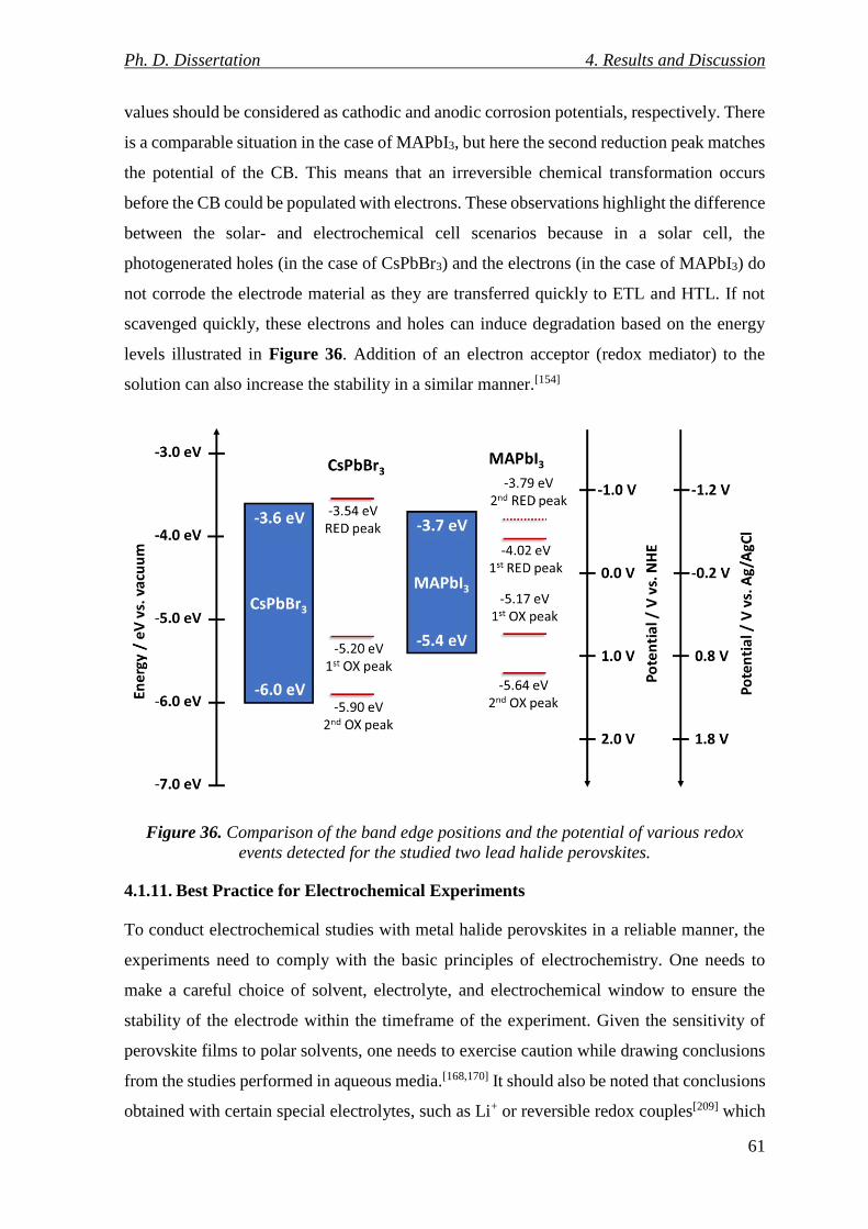
Ph. D. Dissertation 4. Results and Discussion
61
values should be considered as cathodic and anodic corrosion potentials, respectively. There
is a comparable situation in the case of MAPbI3, but here the second reduction peak matches
the potential of the CB. This means that an irreversible chemical transformation occurs
before the CB could be populated with electrons. These observations highlight the difference
between the solar- and electrochemical cell scenarios because in a solar cell, the
photogenerated holes (in the case of CsPbBr3) and the electrons (in the case of MAPbI3) do
not corrode the electrode material as they are transferred quickly to ETL and HTL. If not
scavenged quickly, these electrons and holes can induce degradation based on the energy
levels illustrated in Figure 36. Addition of an electron acceptor (redox mediator) to the
solution can also increase the stability in a similar manner.[154]
Figure 36. Comparison of the band edge positions and the potential of various redox
events detected for the studied two lead halide perovskites.
4.1.11. Best Practice for Electrochemical Experiments
To conduct electrochemical studies with metal halide perovskites in a reliable manner, the
experiments need to comply with the basic principles of electrochemistry. One needs to
make a careful choice of solvent, electrolyte, and electrochemical window to ensure the
stability of the electrode within the timeframe of the experiment. Given the sensitivity of
perovskite films to polar solvents, one needs to exercise caution while drawing conclusions
from the studies performed in aqueous media.[168,170] It should also be noted that conclusions
obtained with certain special electrolytes, such as Li+ or reversible redox couples[209] which
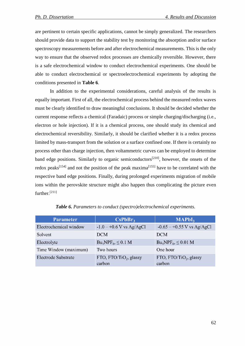
Ph. D. Dissertation 4. Results and Discussion
62
are pertinent to certain specific applications, cannot be simply generalized. The researchers
should provide data to support the stability test by monitoring the absorption and/or surface
spectroscopy measurements before and after electrochemical measurements. This is the only
way to ensure that the observed redox processes are chemically reversible. However, there
is a safe electrochemical window to conduct electrochemical experiments. One should be
able to conduct electrochemical or spectroelectrochemical experiments by adopting the
conditions presented in Table 6.
In addition to the experimental considerations, careful analysis of the results is
equally important. First of all, the electrochemical process behind the measured redox waves
must be clearly identified to draw meaningful conclusions. It should be decided whether the
current response reflects a chemical (Faradaic) process or simple charging/discharging (i.e.,
electron or hole injection). If it is a chemical process, one should study its chemical and
electrochemical reversibility. Similarly, it should be clarified whether it is a redox process
limited by mass-transport from the solution or a surface confined one. If there is certainly no
process other than charge injection, then voltammetric curves can be employed to determine
band edge positions. Similarly to organic semiconductors[210], however, the onsets of the
redox peaks[154] and not the position of the peak maxima[155] have to be correlated with the
respective band edge positions. Finally, during prolonged experiments migration of mobile
ions within the perovskite structure might also happen thus complicating the picture even
further.[211]
Table 6. Parameters to conduct (spectro)electrochemical experiments.
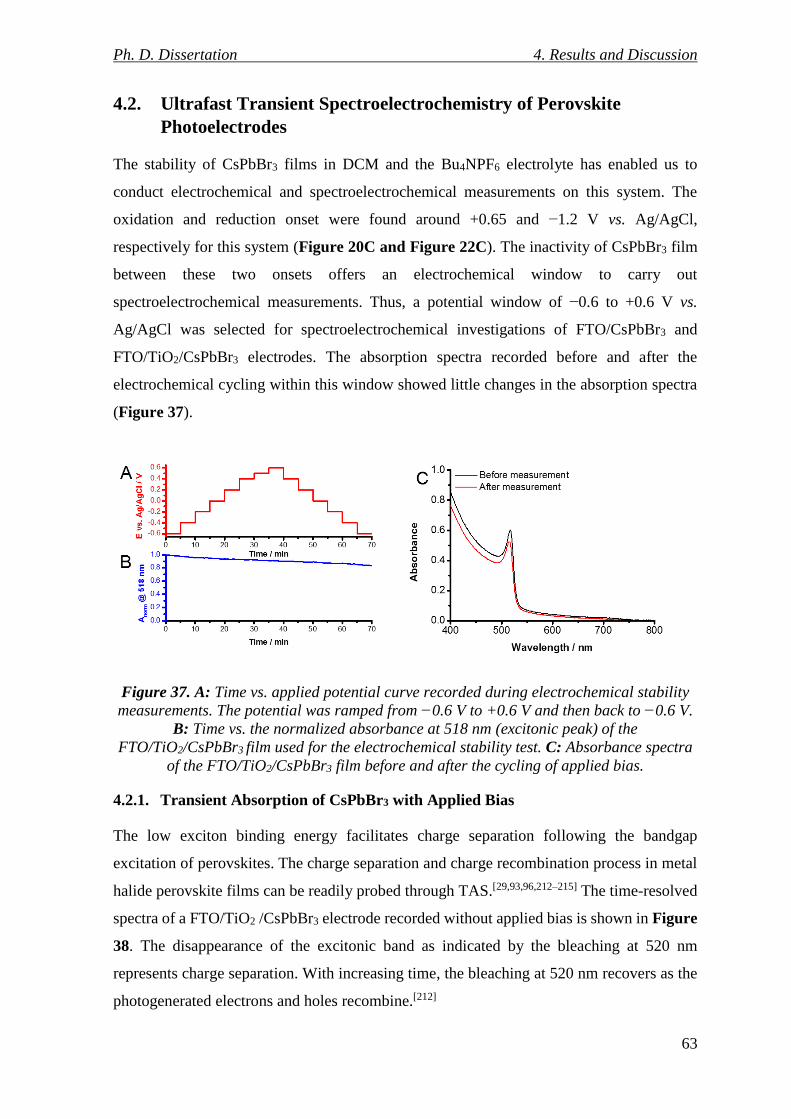
Ph. D. Dissertation 4. Results and Discussion
63
4.2. Ultrafast Transient Spectroelectrochemistry of Perovskite
Photoelectrodes
The stability of CsPbBr3 films in DCM and the Bu4NPF6 electrolyte has enabled us to
conduct electrochemical and spectroelectrochemical measurements on this system. The
oxidation and reduction onset were found around +0.65 and −1.2 V vs. Ag/AgCl,
respectively for this system (Figure 20C and Figure 22C). The inactivity of CsPbBr3 film
between these two onsets offers an electrochemical window to carry out
spectroelectrochemical measurements. Thus, a potential window of −0.6 to +0.6 V vs.
Ag/AgCl was selected for spectroelectrochemical investigations of FTO/CsPbBr3 and
FTO/TiO2/CsPbBr3 electrodes. The absorption spectra recorded before and after the
electrochemical cycling within this window showed little changes in the absorption spectra
(Figure 37).
Figure 37. A: Time vs. applied potential curve recorded during electrochemical stability
measurements. The potential was ramped from −0.6 V to +0.6 V and then back to −0.6 V.
B: Time vs. the normalized absorbance at 518 nm (excitonic peak) of the
FTO/TiO2/CsPbBr3 film used for the electrochemical stability test. C: Absorbance spectra
of the FTO/TiO2/CsPbBr3 film before and after the cycling of applied bias.
4.2.1. Transient Absorption of CsPbBr3 with Applied Bias
The low exciton binding energy facilitates charge separation following the bandgap
excitation of perovskites. The charge separation and charge recombination process in metal
halide perovskite films can be readily probed through TAS.[29,93,96,212–215] The time-resolved
spectra of a FTO/TiO2 /CsPbBr3 electrode recorded without applied bias is shown in Figure
38. The disappearance of the excitonic band as indicated by the bleaching at 520 nm
represents charge separation. With increasing time, the bleaching at 520 nm recovers as the
photogenerated electrons and holes recombine.[212]
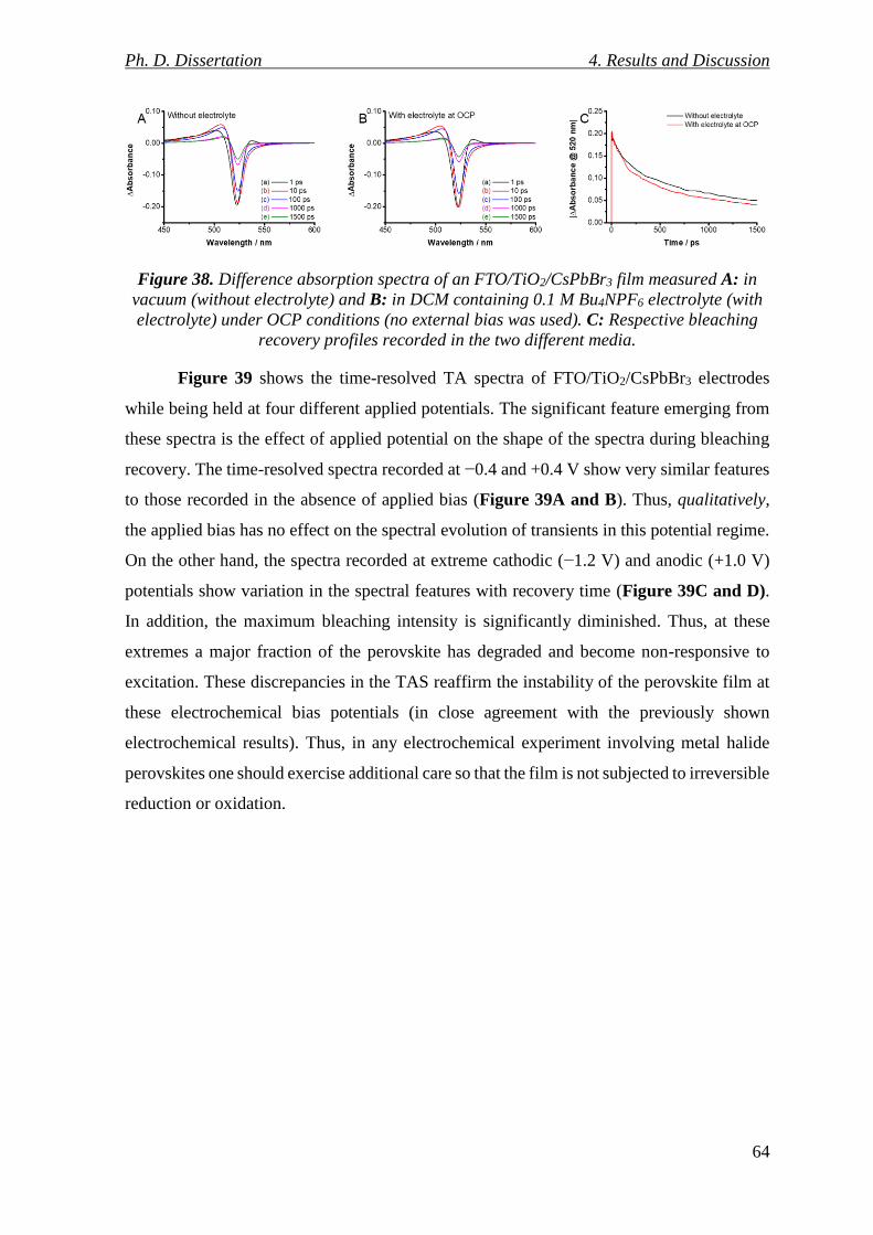
Ph. D. Dissertation 4. Results and Discussion
64
Figure 38. Difference absorption spectra of an FTO/TiO2/CsPbBr3 film measured A: in
vacuum (without electrolyte) and B: in DCM containing 0.1 M Bu4NPF6 electrolyte (with
electrolyte) under OCP conditions (no external bias was used). C: Respective bleaching
recovery profiles recorded in the two different media.
Figure 39 shows the time-resolved TA spectra of FTO/TiO2/CsPbBr3 electrodes
while being held at four different applied potentials. The significant feature emerging from
these spectra is the effect of applied potential on the shape of the spectra during bleaching
recovery. The time-resolved spectra recorded at −0.4 and +0.4 V show very similar features
to those recorded in the absence of applied bias (Figure 39A and B). Thus, qualitatively,
the applied bias has no effect on the spectral evolution of transients in this potential regime.
On the other hand, the spectra recorded at extreme cathodic (−1.2 V) and anodic (+1.0 V)
potentials show variation in the spectral features with recovery time (Figure 39C and D).
In addition, the maximum bleaching intensity is significantly diminished. Thus, at these
extremes a major fraction of the perovskite has degraded and become non-responsive to
excitation. These discrepancies in the TAS reaffirm the instability of the perovskite film at
these electrochemical bias potentials (in close agreement with the previously shown
electrochemical results). Thus, in any electrochemical experiment involving metal halide
perovskites one should exercise additional care so that the film is not subjected to irreversible
reduction or oxidation.
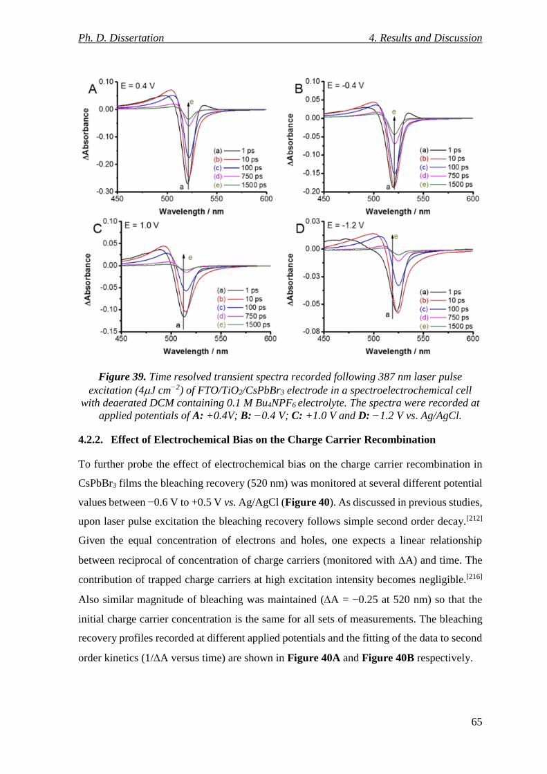
Ph. D. Dissertation 4. Results and Discussion
65
Figure 39. Time resolved transient spectra recorded following 387 nm laser pulse
excitation (4J cm−2) of FTO/TiO2/CsPbBr3 electrode in a spectroelectrochemical cell
with deaerated DCM containing 0.1 M Bu4NPF6 electrolyte. The spectra were recorded at
applied potentials of A: +0.4V; B: −0.4 V; C: +1.0 V and D: −1.2 V vs. Ag/AgCl.
4.2.2. Effect of Electrochemical Bias on the Charge Carrier Recombination
To further probe the effect of electrochemical bias on the charge carrier recombination in
CsPbBr3 films the bleaching recovery (520 nm) was monitored at several different potential
values between −0.6 V to +0.5 V vs. Ag/AgCl (Figure 40). As discussed in previous studies,
upon laser pulse excitation the bleaching recovery follows simple second order decay.[212]
Given the equal concentration of electrons and holes, one expects a linear relationship
between reciprocal of concentration of charge carriers (monitored with A) and time. The
contribution of trapped charge carriers at high excitation intensity becomes negligible.[216]
Also similar magnitude of bleaching was maintained (A = −0.25 at 520 nm) so that the
initial charge carrier concentration is the same for all sets of measurements. The bleaching
recovery profiles recorded at different applied potentials and the fitting of the data to second
order kinetics (1/A versus time) are shown in Figure 40A and Figure 40B respectively.
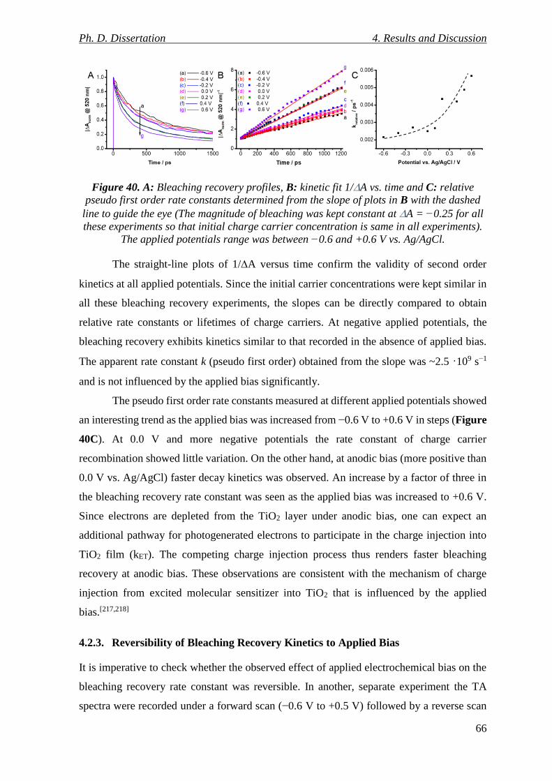
Ph. D. Dissertation 4. Results and Discussion
66
Figure 40. A: Bleaching recovery profiles, B: kinetic fit 1/A vs. time and C: relative
pseudo first order rate constants determined from the slope of plots in B with the dashed
line to guide the eye (The magnitude of bleaching was kept constant at A = −0.25 for all
these experiments so that initial charge carrier concentration is same in all experiments).
The applied potentials range was between −0.6 and +0.6 V vs. Ag/AgCl.
The straight-line plots of 1/A versus time confirm the validity of second order
kinetics at all applied potentials. Since the initial carrier concentrations were kept similar in
all these bleaching recovery experiments, the slopes can be directly compared to obtain
relative rate constants or lifetimes of charge carriers. At negative applied potentials, the
bleaching recovery exhibits kinetics similar to that recorded in the absence of applied bias.
The apparent rate constant k (pseudo first order) obtained from the slope was ~2.5 ·109 s−1
and is not influenced by the applied bias significantly.
The pseudo first order rate constants measured at different applied potentials showed
an interesting trend as the applied bias was increased from −0.6 V to +0.6 V in steps (Figure
40C). At 0.0 V and more negative potentials the rate constant of charge carrier
recombination showed little variation. On the other hand, at anodic bias (more positive than
0.0 V vs. Ag/AgCl) faster decay kinetics was observed. An increase by a factor of three in
the bleaching recovery rate constant was seen as the applied bias was increased to +0.6 V.
Since electrons are depleted from the TiO2 layer under anodic bias, one can expect an
additional pathway for photogenerated electrons to participate in the charge injection into
TiO2 film (kET). The competing charge injection process thus renders faster bleaching
recovery at anodic bias. These observations are consistent with the mechanism of charge
injection from excited molecular sensitizer into TiO2 that is influenced by the applied
bias.[217,218]
4.2.3. Reversibility of Bleaching Recovery Kinetics to Applied Bias
It is imperative to check whether the observed effect of applied electrochemical bias on the
bleaching recovery rate constant was reversible. In another, separate experiment the TA
spectra were recorded under a forward scan (−0.6 V to +0.5 V) followed by a reverse scan
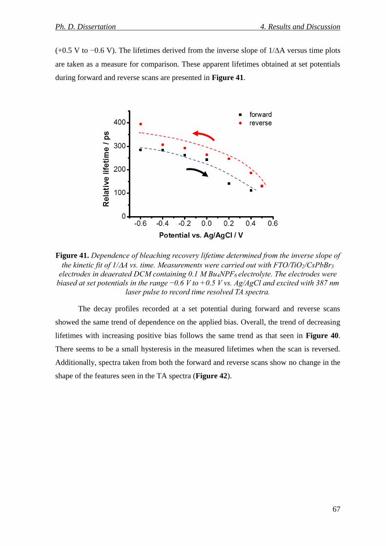
Ph. D. Dissertation 4. Results and Discussion
67
(+0.5 V to −0.6 V). The lifetimes derived from the inverse slope of 1/A versus time plots
are taken as a measure for comparison. These apparent lifetimes obtained at set potentials
during forward and reverse scans are presented in Figure 41.
Figure 41. Dependence of bleaching recovery lifetime determined from the inverse slope of
the kinetic fit of 1/A vs. time. Measurements were carried out with FTO/TiO2/CsPbBr3
electrodes in deaerated DCM containing 0.1 M Bu4NPF6 electrolyte. The electrodes were
biased at set potentials in the range −0.6 V to +0.5 V vs. Ag/AgCl and excited with 387 nm
laser pulse to record time resolved TA spectra.
The decay profiles recorded at a set potential during forward and reverse scans
showed the same trend of dependence on the applied bias. Overall, the trend of decreasing
lifetimes with increasing positive bias follows the same trend as that seen in Figure 40.
There seems to be a small hysteresis in the measured lifetimes when the scan is reversed.
Additionally, spectra taken from both the forward and reverse scans show no change in the
shape of the features seen in the TA spectra (Figure 42).
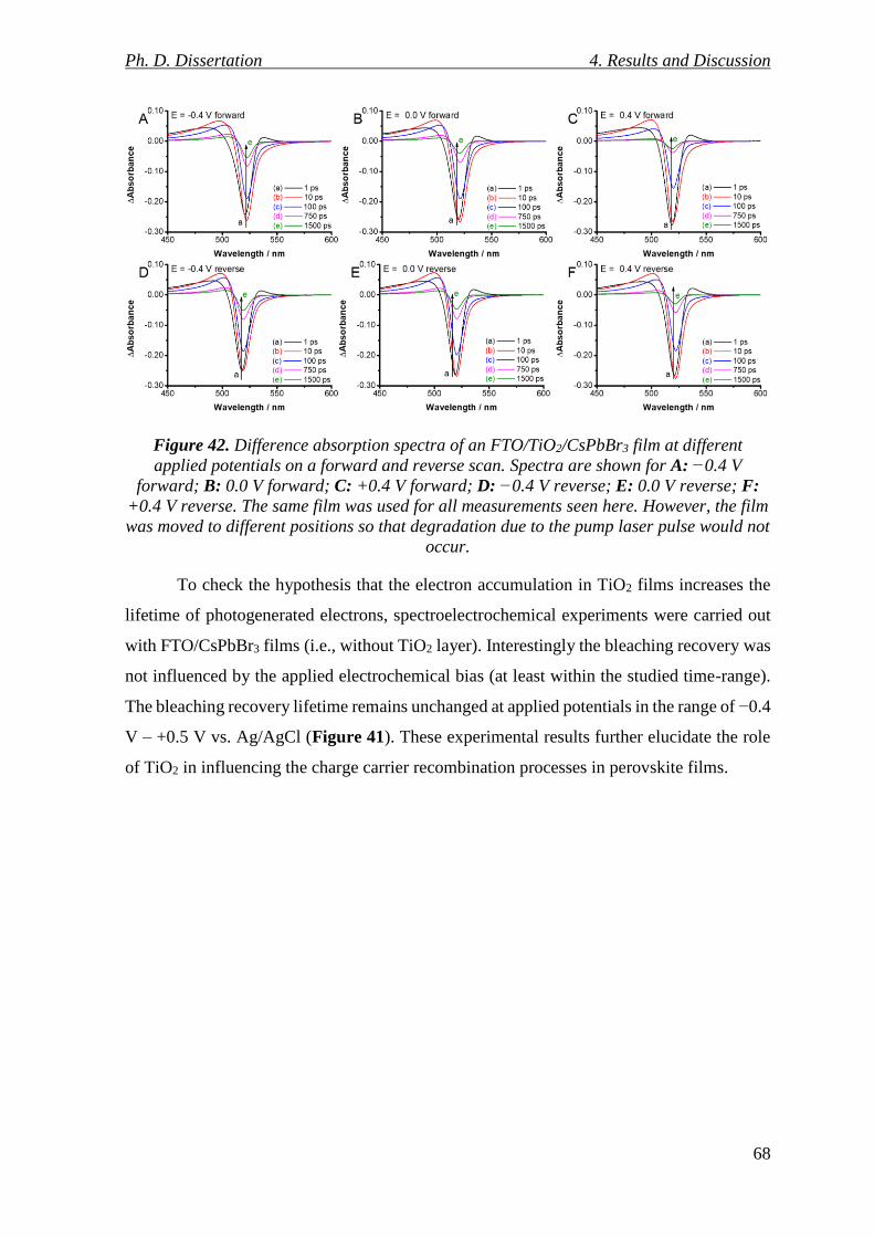
Ph. D. Dissertation 4. Results and Discussion
68
Figure 42. Difference absorption spectra of an FTO/TiO2/CsPbBr3 film at different
applied potentials on a forward and reverse scan. Spectra are shown for A: −0.4 V
forward; B: 0.0 V forward; C: +0.4 V forward; D: −0.4 V reverse; E: 0.0 V reverse; F:
+0.4 V reverse. The same film was used for all measurements seen here. However, the film
was moved to different positions so that degradation due to the pump laser pulse would not
occur.
To check the hypothesis that the electron accumulation in TiO2 films increases the
lifetime of photogenerated electrons, spectroelectrochemical experiments were carried out
with FTO/CsPbBr3 films (i.e., without TiO2 layer). Interestingly the bleaching recovery was
not influenced by the applied electrochemical bias (at least within the studied time-range).
The bleaching recovery lifetime remains unchanged at applied potentials in the range of −0.4
V – +0.5 V vs. Ag/AgCl (Figure 41). These experimental results further elucidate the role
of TiO2 in influencing the charge carrier recombination processes in perovskite films.
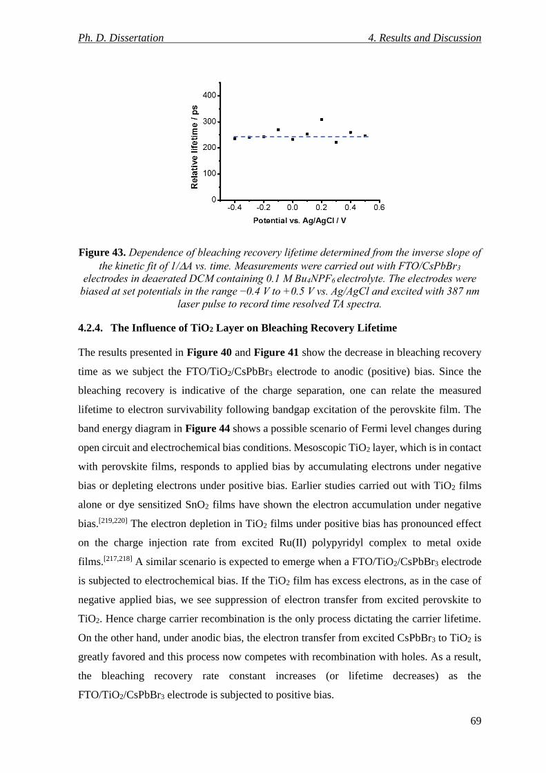
Ph. D. Dissertation 4. Results and Discussion
69
Figure 43. Dependence of bleaching recovery lifetime determined from the inverse slope of
the kinetic fit of 1/A vs. time. Measurements were carried out with FTO/CsPbBr3
electrodes in deaerated DCM containing 0.1 M Bu4NPF6 electrolyte. The electrodes were
biased at set potentials in the range −0.4 V to +0.5 V vs. Ag/AgCl and excited with 387 nm
laser pulse to record time resolved TA spectra.
4.2.4. The Influence of TiO2 Layer on Bleaching Recovery Lifetime
The results presented in Figure 40 and Figure 41 show the decrease in bleaching recovery
time as we subject the FTO/TiO2/CsPbBr3 electrode to anodic (positive) bias. Since the
bleaching recovery is indicative of the charge separation, one can relate the measured
lifetime to electron survivability following bandgap excitation of the perovskite film. The
band energy diagram in Figure 44 shows a possible scenario of Fermi level changes during
open circuit and electrochemical bias conditions. Mesoscopic TiO2 layer, which is in contact
with perovskite films, responds to applied bias by accumulating electrons under negative
bias or depleting electrons under positive bias. Earlier studies carried out with TiO2 films
alone or dye sensitized SnO2 films have shown the electron accumulation under negative
bias.[219,220] The electron depletion in TiO2 films under positive bias has pronounced effect
on the charge injection rate from excited Ru(II) polypyridyl complex to metal oxide
films.[217,218] A similar scenario is expected to emerge when a FTO/TiO2/CsPbBr3 electrode
is subjected to electrochemical bias. If the TiO2 film has excess electrons, as in the case of
negative applied bias, we see suppression of electron transfer from excited perovskite to
TiO2. Hence charge carrier recombination is the only process dictating the carrier lifetime.
On the other hand, under anodic bias, the electron transfer from excited CsPbBr3 to TiO2 is
greatly favored and this process now competes with recombination with holes. As a result,
the bleaching recovery rate constant increases (or lifetime decreases) as the
FTO/TiO2/CsPbBr3 electrode is subjected to positive bias.
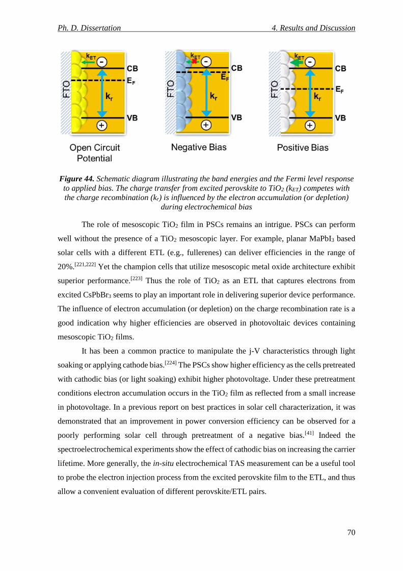
Ph. D. Dissertation 4. Results and Discussion
70
Figure 44. Schematic diagram illustrating the band energies and the Fermi level response
to applied bias. The charge transfer from excited perovskite to TiO2 (kET) competes with
the charge recombination (kr) is influenced by the electron accumulation (or depletion)
during electrochemical bias
The role of mesoscopic TiO2 film in PSCs remains an intrigue. PSCs can perform
well without the presence of a TiO2 mesoscopic layer. For example, planar MaPbI3 based
solar cells with a different ETL (e.g., fullerenes) can deliver efficiencies in the range of
20%.[221,222] Yet the champion cells that utilize mesoscopic metal oxide architecture exhibit
superior performance.[223] Thus the role of TiO2 as an ETL that captures electrons from
excited CsPbBr3 seems to play an important role in delivering superior device performance.
The influence of electron accumulation (or depletion) on the charge recombination rate is a
good indication why higher efficiencies are observed in photovoltaic devices containing
mesoscopic TiO2 films.
It has been a common practice to manipulate the j-V characteristics through light
soaking or applying cathode bias.[224] The PSCs show higher efficiency as the cells pretreated
with cathodic bias (or light soaking) exhibit higher photovoltage. Under these pretreatment
conditions electron accumulation occurs in the TiO2 film as reflected from a small increase
in photovoltage. In a previous report on best practices in solar cell characterization, it was
demonstrated that an improvement in power conversion efficiency can be observed for a
poorly performing solar cell through pretreatment of a negative bias.[41] Indeed the
spectroelectrochemical experiments show the effect of cathodic bias on increasing the carrier
lifetime. More generally, the in-situ electrochemical TAS measurement can be a useful tool
to probe the electron injection process from the excited perovskite film to the ETL, and thus
allow a convenient evaluation of different perovskite/ETL pairs.
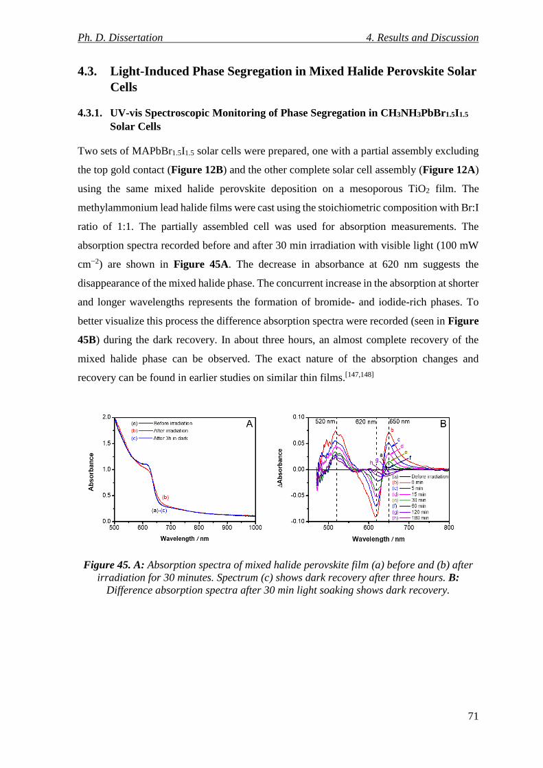
Ph. D. Dissertation 4. Results and Discussion
71
4.3. Light-Induced Phase Segregation in Mixed Halide Perovskite Solar
Cells
4.3.1. UV-vis Spectroscopic Monitoring of Phase Segregation in CH3NH3PbBr1.5I1.5
Solar Cells
Two sets of MAPbBr1.5I1.5 solar cells were prepared, one with a partial assembly excluding
the top gold contact (Figure 12B) and the other complete solar cell assembly (Figure 12A)
using the same mixed halide perovskite deposition on a mesoporous TiO2 film. The
methylammonium lead halide films were cast using the stoichiometric composition with Br:I
ratio of 1:1. The partially assembled cell was used for absorption measurements. The
absorption spectra recorded before and after 30 min irradiation with visible light (100 mW
cm−2) are shown in Figure 45A. The decrease in absorbance at 620 nm suggests the
disappearance of the mixed halide phase. The concurrent increase in the absorption at shorter
and longer wavelengths represents the formation of bromide- and iodide-rich phases. To
better visualize this process the difference absorption spectra were recorded (seen in Figure
45B) during the dark recovery. In about three hours, an almost complete recovery of the
mixed halide phase can be observed. The exact nature of the absorption changes and
recovery can be found in earlier studies on similar thin films.[147,148]
Figure 45. A: Absorption spectra of mixed halide perovskite film (a) before and (b) after
irradiation for 30 minutes. Spectrum (c) shows dark recovery after three hours. B:
Difference absorption spectra after 30 min light soaking shows dark recovery.
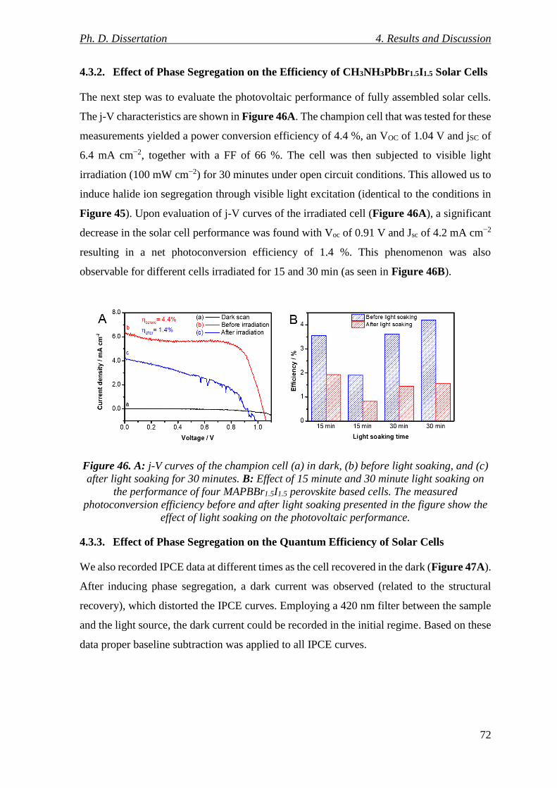
Ph. D. Dissertation 4. Results and Discussion
72
4.3.2. Effect of Phase Segregation on the Efficiency of CH3NH3PbBr1.5I1.5 Solar Cells
The next step was to evaluate the photovoltaic performance of fully assembled solar cells.
The j-V characteristics are shown in Figure 46A. The champion cell that was tested for these
measurements yielded a power conversion efficiency of 4.4 %, an VOC of 1.04 V and jSC of
6.4 mA cm−2, together with a FF of 66 %. The cell was then subjected to visible light
irradiation (100 mW cm−2) for 30 minutes under open circuit conditions. This allowed us to
induce halide ion segregation through visible light excitation (identical to the conditions in
Figure 45). Upon evaluation of j-V curves of the irradiated cell (Figure 46A), a significant
decrease in the solar cell performance was found with Voc of 0.91 V and Jsc of 4.2 mA cm−2
resulting in a net photoconversion efficiency of 1.4 %. This phenomenon was also
observable for different cells irradiated for 15 and 30 min (as seen in Figure 46B).
Figure 46. A: j-V curves of the champion cell (a) in dark, (b) before light soaking, and (c)
after light soaking for 30 minutes. B: Effect of 15 minute and 30 minute light soaking on
the performance of four MAPBBr1.5I1.5 perovskite based cells. The measured
photoconversion efficiency before and after light soaking presented in the figure show the
effect of light soaking on the photovoltaic performance.
4.3.3. Effect of Phase Segregation on the Quantum Efficiency of Solar Cells
We also recorded IPCE data at different times as the cell recovered in the dark (Figure 47A).
After inducing phase segregation, a dark current was observed (related to the structural
recovery), which distorted the IPCE curves. Employing a 420 nm filter between the sample
and the light source, the dark current could be recorded in the initial regime. Based on these
data proper baseline subtraction was applied to all IPCE curves.
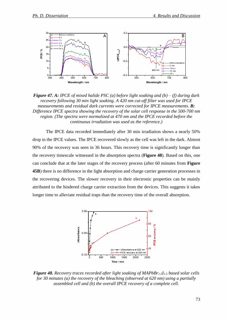
Ph. D. Dissertation 4. Results and Discussion
73
Figure 47. A: IPCE of mixed halide PSC (a) before light soaking and (b) – (f) during dark
recovery following 30 min light soaking. A 420 nm cut-off filter was used for IPCE
measurements and residual dark currents were corrected for IPCE measurements. B:
Difference IPCE spectra showing the recovery of the solar cell response in the 500-700 nm
region. (The spectra were normalized at 470 nm and the IPCE recorded before the
continuous irradiation was used as the reference.)
The IPCE data recorded immediately after 30 min irradiation shows a nearly 50%
drop in the IPCE values. The IPCE recovered slowly as the cell was left in the dark. Almost
90% of the recovery was seen in 36 hours. This recovery time is significantly longer than
the recovery timescale witnessed in the absorption spectra (Figure 48). Based on this, one
can conclude that at the later stages of the recovery process (after 60 minutes from Figure
45B) there is no difference in the light absorption and charge carrier generation processes in
the recovering devices. The slower recovery in their electronic properties can be mainly
attributed to the hindered charge carrier extraction from the devices. This suggests it takes
longer time to alleviate residual traps than the recovery time of the overall absorption.
Figure 48. Recovery traces recorded after light soaking of MAPbBr1.5I1.5 based solar cells
for 30 minutes (a) the recovery of the bleaching (observed at 620 nm) using a partially
assembled cell and (b) the overall IPCE recovery of a complete cell.
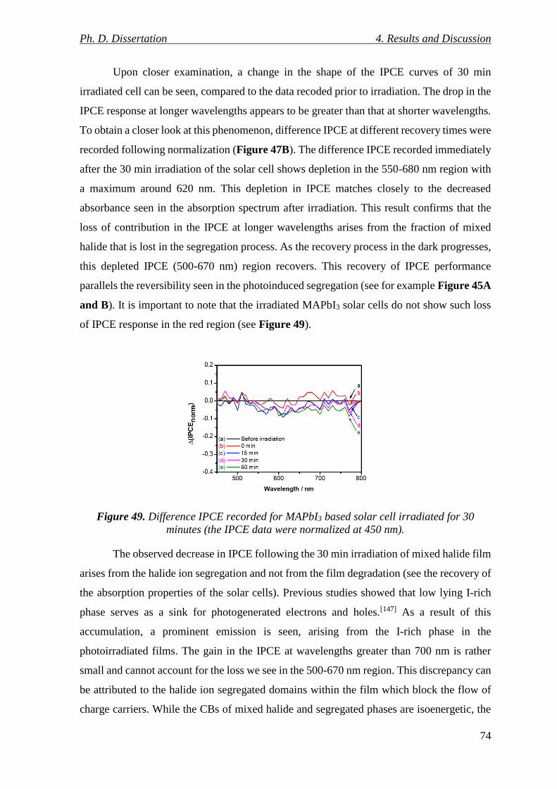
Ph. D. Dissertation 4. Results and Discussion
74
Upon closer examination, a change in the shape of the IPCE curves of 30 min
irradiated cell can be seen, compared to the data recoded prior to irradiation. The drop in the
IPCE response at longer wavelengths appears to be greater than that at shorter wavelengths.
To obtain a closer look at this phenomenon, difference IPCE at different recovery times were
recorded following normalization (Figure 47B). The difference IPCE recorded immediately
after the 30 min irradiation of the solar cell shows depletion in the 550-680 nm region with
a maximum around 620 nm. This depletion in IPCE matches closely to the decreased
absorbance seen in the absorption spectrum after irradiation. This result confirms that the
loss of contribution in the IPCE at longer wavelengths arises from the fraction of mixed
halide that is lost in the segregation process. As the recovery process in the dark progresses,
this depleted IPCE (500-670 nm) region recovers. This recovery of IPCE performance
parallels the reversibility seen in the photoinduced segregation (see for example Figure 45A
and B). It is important to note that the irradiated MAPbI3 solar cells do not show such loss
of IPCE response in the red region (see Figure 49).
Figure 49. Difference IPCE recorded for MAPbI3 based solar cell irradiated for 30
minutes (the IPCE data were normalized at 450 nm).
The observed decrease in IPCE following the 30 min irradiation of mixed halide film
arises from the halide ion segregation and not from the film degradation (see the recovery of
the absorption properties of the solar cells). Previous studies showed that low lying I-rich
phase serves as a sink for photogenerated electrons and holes.[147] As a result of this
accumulation, a prominent emission is seen, arising from the I-rich phase in the
photoirradiated films. The gain in the IPCE at wavelengths greater than 700 nm is rather
small and cannot account for the loss we see in the 500-670 nm region. This discrepancy can
be attributed to the halide ion segregated domains within the film which block the flow of
charge carriers. While the CBs of mixed halide and segregated phases are isoenergetic, the

Ph. D. Dissertation 4. Results and Discussion
75
VBs show an energy gradient causing I-rich region to favor the hole accumulation (Figure
50). The I-rich domains thus serve as recombination centers resulting in an eventual decrease
in the IPCE and the overall photoconversion efficiency.[78,80,147] As the mixed films recover
in the dark, these recombination centers are removed and we see the recovery of photovoltaic
performance.
Figure 50. Schematic representation of phase segregation in mixed-halide (MAPbBr1.5I1.5)
solar cells, and its effect on the charge collection of such devices.

Ph. D. Dissertation 4. Results and Discussion
76
4.4. Electrosynthesis of PEDOT Hole Transporter Layer on
CH3NH3PbI3 Electrodes
4.4.1. Spectroelectrochemistry of PEDOT Deposition on CH3NH3PbI3 Electrodes
To monitor the optical changes during electrodeposition, FTO/TiO2/MAPbI3 electrodes with
a thin MAPbI3 layer were fabricated (Figure 12C). In the previous section we established
that in 0.1 M Bu4NPF6/DCM electrolyte, the MAPbI3 layers remain intact (less than 10%
degradation) for around 10 minutes (Figure 32). Note that it was not possible to employ
lower electrolyte concentration in this case, because the conductivity of the solution had to
be also considered. Furthermore, it had to be ensured that the MAPbI3 layer remains intact
during the oxidative electropolymerization. Interestingly, MAPbI3 layers proved to be more
resistant to oxidation than reduction (Figure 33). However, EDOT cannot be used as the
polymerization precursor, because its polymerization potential would exceed the
electrochemical stability window of MAPbI3. To circumvent this issue bis-EDOT was used
instead, which in turn allowed the oxidative electropolymerization of PEDOT without
degrading the MAPbI3 layer. The polymerization potential can be effectively lowered by
using the dimeric unit of a conducting polymer instead of the monomeric unit, caused by the
increased conjugation length of the dimer.[225]
To determine the electropolymerization potential of bis-EDOT on
FTO/TiO2/MAPbI3 electrodes, in situ spectroelectrochemical experiments were carried out
(Figure 51A-C). The gradual growth of PEDOT was observed during potentiodynamic
deposition, indicated by the increasing capacitive current in the range of 0.0 V – +0.6 V
(Figure 51A). The peak at 450 nm on the UV-vis spectrum could be attributed to EDOT
oligomers (in the solution) and the broad absorbance between 500 – 800 nm to the formation
of the PEDOT layer (Figure 51B). To determine the polymerization potential of bis-EDOT
on this architecture, the first polymerization half cycle was plotted together with the
absorbance increase at 700 nm in Figure 51C. A sharp rise in the current at +0.7 V was
observed, which was accompanied by the absorbance increase at 700 nm, confirming the
polymerization of bis-EDOT.
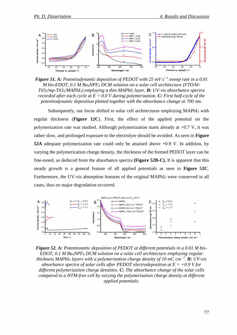
Ph. D. Dissertation 4. Results and Discussion
77
Figure 51. A: Potentiodynamic deposition of PEDOT with 25 mV s−1 sweep rate in a 0.01
M bis-EDOT, 0.1 M Bu4NPF6 DCM solution on a solar cell architecture (FTO/bl-
TiO2/mp-TiO2/MAPbI3) employing a thin MAPbI3 layer. B: UV-vis absorbance spectra
recorded after each cycle at E = 0.0 V during polymerization. C: First half-cycle of the
potentiodynamic deposition plotted together with the absorbance change at 700 nm.
Subsequently, our focus shifted to solar cell architectures employing MAPbI3 with
regular thickness (Figure 12C). First, the effect of the applied potential on the
polymerization rate was studied. Although polymerization starts already at +0.7 V, it was
rather slow, and prolonged exposure to the electrolyte should be avoided. As seen in Figure
52A adequate polymerization rate could only be attained above +0.9 V. In addition, by
varying the polymerization charge density, the thickness of the formed PEDOT layer can be
fine-tuned, as deduced from the absorbance spectra (Figure 52B-C). It is apparent that this
steady growth is a general feature of all applied potentials as seen in Figure 52C.
Furthermore, the UV-vis absorption features of the original MAPbI3 were conserved in all
cases, thus no major degradation occurred.
Figure 52. A: Potentiostatic deposition of PEDOT at different potentials in a 0.01 M bis-
EDOT, 0.1 M Bu4NPF6 DCM solution on a solar cell architecture employing regular
thickness MAPbI3 layers with a polymerization charge density of 10 mC cm−2. B: UV-vis
absorbance spectra of solar cells after PEDOT electrodeposition at E = +0.9 V for
different polymerization charge densities. C: The absorbance change of the solar cells
compared to a HTM-free cell by varying the polymerization charge density at different
applied potentials.
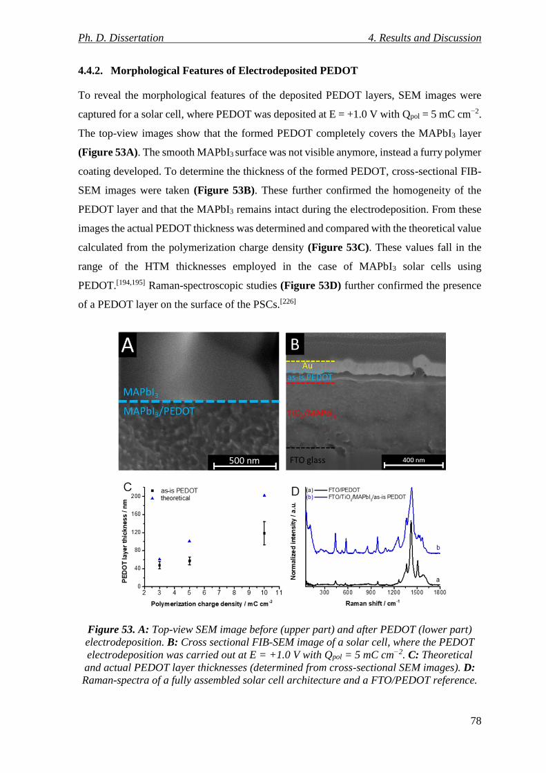
Ph. D. Dissertation 4. Results and Discussion
78
4.4.2. Morphological Features of Electrodeposited PEDOT
To reveal the morphological features of the deposited PEDOT layers, SEM images were
captured for a solar cell, where PEDOT was deposited at E = +1.0 V with Qpol = 5 mC cm−2.
The top-view images show that the formed PEDOT completely covers the MAPbI3 layer
(Figure 53A). The smooth MAPbI3 surface was not visible anymore, instead a furry polymer
coating developed. To determine the thickness of the formed PEDOT, cross-sectional FIB-
SEM images were taken (Figure 53B). These further confirmed the homogeneity of the
PEDOT layer and that the MAPbI3 remains intact during the electrodeposition. From these
images the actual PEDOT thickness was determined and compared with the theoretical value
calculated from the polymerization charge density (Figure 53C). These values fall in the
range of the HTM thicknesses employed in the case of MAPbI3 solar cells using
PEDOT.[194,195] Raman-spectroscopic studies (Figure 53D) further confirmed the presence
of a PEDOT layer on the surface of the PSCs.[226]
Figure 53. A: Top-view SEM image before (upper part) and after PEDOT (lower part)
electrodeposition. B: Cross sectional FIB-SEM image of a solar cell, where the PEDOT
electrodeposition was carried out at E = +1.0 V with Qpol = 5 mC cm−2. C: Theoretical
and actual PEDOT layer thicknesses (determined from cross-sectional SEM images). D:
Raman-spectra of a fully assembled solar cell architecture and a FTO/PEDOT reference.
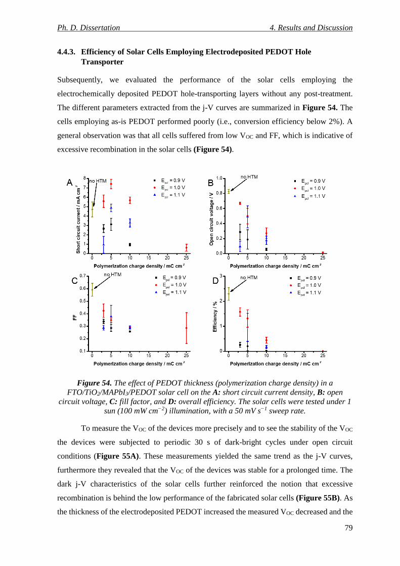
Ph. D. Dissertation 4. Results and Discussion
79
4.4.3. Efficiency of Solar Cells Employing Electrodeposited PEDOT Hole
Transporter
Subsequently, we evaluated the performance of the solar cells employing the
electrochemically deposited PEDOT hole-transporting layers without any post-treatment.
The different parameters extracted from the j-V curves are summarized in Figure 54. The
cells employing as-is PEDOT performed poorly (i.e., conversion efficiency below 2%). A
general observation was that all cells suffered from low VOC and FF, which is indicative of
excessive recombination in the solar cells (Figure 54).
Figure 54. The effect of PEDOT thickness (polymerization charge density) in a
FTO/TiO2/MAPbI3/PEDOT solar cell on the A: short circuit current density, B: open
circuit voltage, C: fill factor, and D: overall efficiency. The solar cells were tested under 1
sun (100 mW cm−2) illumination, with a 50 mV s−1 sweep rate.
To measure the VOC of the devices more precisely and to see the stability of the VOC
the devices were subjected to periodic 30 s of dark-bright cycles under open circuit
conditions (Figure 55A). These measurements yielded the same trend as the j-V curves,
furthermore they revealed that the VOC of the devices was stable for a prolonged time. The
dark j-V characteristics of the solar cells further reinforced the notion that excessive
recombination is behind the low performance of the fabricated solar cells (Figure 55B). As
the thickness of the electrodeposited PEDOT increased the measured VOC decreased and the
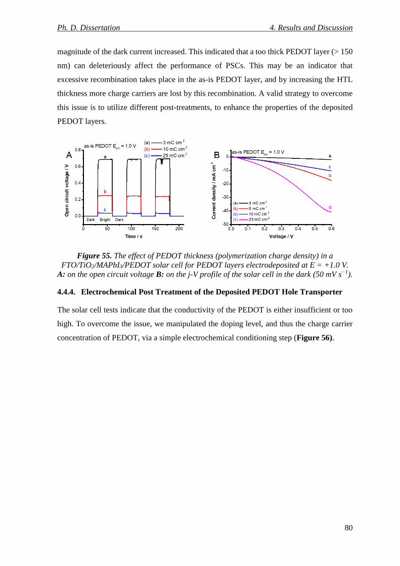
Ph. D. Dissertation 4. Results and Discussion
80
magnitude of the dark current increased. This indicated that a too thick PEDOT layer (> 150
nm) can deleteriously affect the performance of PSCs. This may be an indicator that
excessive recombination takes place in the as-is PEDOT layer, and by increasing the HTL
thickness more charge carriers are lost by this recombination. A valid strategy to overcome
this issue is to utilize different post-treatments, to enhance the properties of the deposited
PEDOT layers.
Figure 55. The effect of PEDOT thickness (polymerization charge density) in a
FTO/TiO2/MAPbI3/PEDOT solar cell for PEDOT layers electrodeposited at E = +1.0 V.
A: on the open circuit voltage B: on the j-V profile of the solar cell in the dark (50 mV s−1).
4.4.4. Electrochemical Post Treatment of the Deposited PEDOT Hole Transporter
The solar cell tests indicate that the conductivity of the PEDOT is either insufficient or too
high. To overcome the issue, we manipulated the doping level, and thus the charge carrier
concentration of PEDOT, via a simple electrochemical conditioning step (Figure 56).
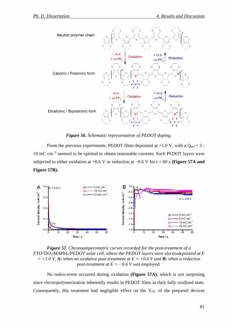
Ph. D. Dissertation 4. Results and Discussion
81
Figure 56. Schematic representation of PEDOT doping.
From the previous experiments, PEDOT films deposited at +1.0 V, with a Qpol = 3 -
10 mC cm−2 seemed to be optimal to obtain reasonable currents. Such PEDOT layers were
subjected to either oxidation at +0.6 V or reduction at −0.6 V for t = 60 s (Figure 57A and
Figure 57B).
Figure 57. Chronoamperometric curves recorded for the post-treatment of a
FTO/TiO2/MAPbI3/PEDOT solar cell, where the PEDOT layers were electrodeposited at E
= +1.0 V, A: when an oxidative post-treatment at E = +0.6 V and B: when a reductive
post-treatment at E = −0.6 V was employed.
No redox-event occurred during oxidation (Figure 57A), which is not surprising
since electropolymerization inherently results in PEDOT films in their fully oxidized state.
Consequently, this treatment had negligible effect on the VOC of the prepared devices
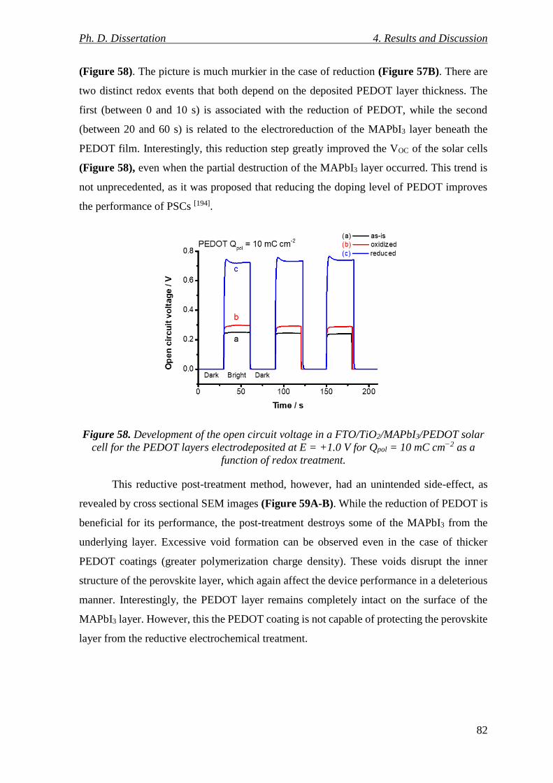
Ph. D. Dissertation 4. Results and Discussion
82
(Figure 58). The picture is much murkier in the case of reduction (Figure 57B). There are
two distinct redox events that both depend on the deposited PEDOT layer thickness. The
first (between 0 and 10 s) is associated with the reduction of PEDOT, while the second
(between 20 and 60 s) is related to the electroreduction of the MAPbI3 layer beneath the
PEDOT film. Interestingly, this reduction step greatly improved the VOC of the solar cells
(Figure 58), even when the partial destruction of the MAPbI3 layer occurred. This trend is
not unprecedented, as it was proposed that reducing the doping level of PEDOT improves
the performance of PSCs [194].
Figure 58. Development of the open circuit voltage in a FTO/TiO2/MAPbI3/PEDOT solar
cell for the PEDOT layers electrodeposited at E = +1.0 V for Qpol = 10 mC cm−2 as a
function of redox treatment.
This reductive post-treatment method, however, had an unintended side-effect, as
revealed by cross sectional SEM images (Figure 59A-B). While the reduction of PEDOT is
beneficial for its performance, the post-treatment destroys some of the MAPbI3 from the
underlying layer. Excessive void formation can be observed even in the case of thicker
PEDOT coatings (greater polymerization charge density). These voids disrupt the inner
structure of the perovskite layer, which again affect the device performance in a deleterious
manner. Interestingly, the PEDOT layer remains completely intact on the surface of the
MAPbI3 layer. However, this the PEDOT coating is not capable of protecting the perovskite
layer from the reductive electrochemical treatment.
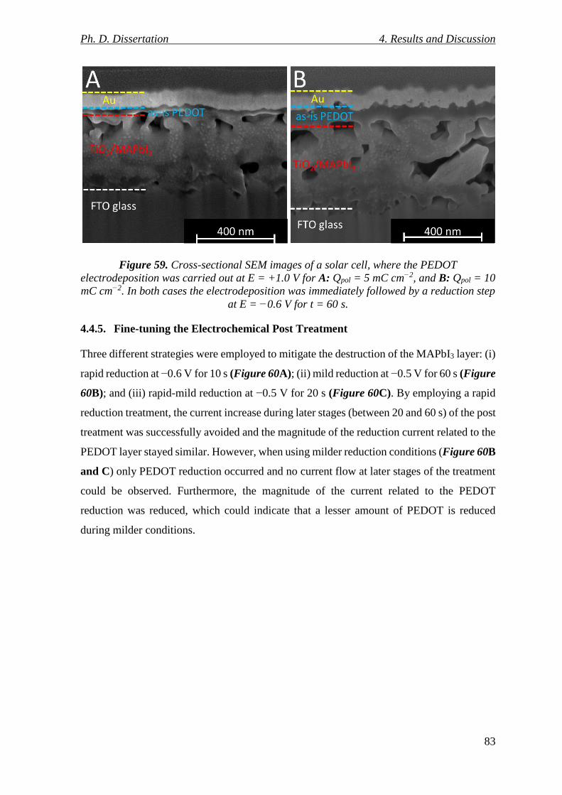
Ph. D. Dissertation 4. Results and Discussion
83
Figure 59. Cross-sectional SEM images of a solar cell, where the PEDOT
electrodeposition was carried out at E = +1.0 V for A: Qpol = 5 mC cm−2, and B: Qpol = 10
mC cm−2. In both cases the electrodeposition was immediately followed by a reduction step
at E = −0.6 V for t = 60 s.
4.4.5. Fine-tuning the Electrochemical Post Treatment
Three different strategies were employed to mitigate the destruction of the MAPbI3 layer: (i)
rapid reduction at −0.6 V for 10 s (Figure 60A); (ii) mild reduction at −0.5 V for 60 s (Figure
60B); and (iii) rapid-mild reduction at −0.5 V for 20 s (Figure 60C). By employing a rapid
reduction treatment, the current increase during later stages (between 20 and 60 s) of the post
treatment was successfully avoided and the magnitude of the reduction current related to the
PEDOT layer stayed similar. However, when using milder reduction conditions (Figure 60B
and C) only PEDOT reduction occurred and no current flow at later stages of the treatment
could be observed. Furthermore, the magnitude of the current related to the PEDOT
reduction was reduced, which could indicate that a lesser amount of PEDOT is reduced
during milder conditions.
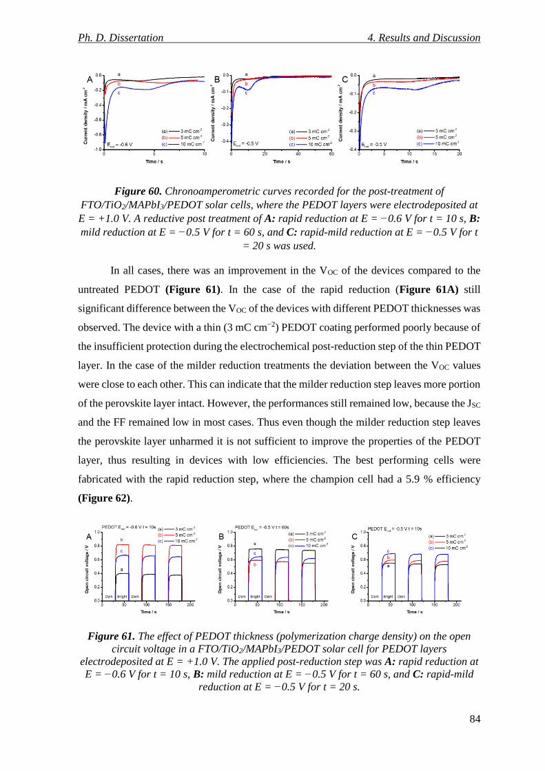
Ph. D. Dissertation 4. Results and Discussion
84
Figure 60. Chronoamperometric curves recorded for the post-treatment of
FTO/TiO2/MAPbI3/PEDOT solar cells, where the PEDOT layers were electrodeposited at
E = +1.0 V. A reductive post treatment of A: rapid reduction at E = −0.6 V for t = 10 s, B:
mild reduction at E = −0.5 V for t = 60 s, and C: rapid-mild reduction at E = −0.5 V for t
= 20 s was used.
In all cases, there was an improvement in the VOC of the devices compared to the
untreated PEDOT (Figure 61). In the case of the rapid reduction (Figure 61A) still
significant difference between the VOC of the devices with different PEDOT thicknesses was
observed. The device with a thin (3 mC cm−2) PEDOT coating performed poorly because of
the insufficient protection during the electrochemical post-reduction step of the thin PEDOT
layer. In the case of the milder reduction treatments the deviation between the VOC values
were close to each other. This can indicate that the milder reduction step leaves more portion
of the perovskite layer intact. However, the performances still remained low, because the JSC
and the FF remained low in most cases. Thus even though the milder reduction step leaves
the perovskite layer unharmed it is not sufficient to improve the properties of the PEDOT
layer, thus resulting in devices with low efficiencies. The best performing cells were
fabricated with the rapid reduction step, where the champion cell had a 5.9 % efficiency
(Figure 62).
Figure 61. The effect of PEDOT thickness (polymerization charge density) on the open
circuit voltage in a FTO/TiO2/MAPbI3/PEDOT solar cell for PEDOT layers
electrodeposited at E = +1.0 V. The applied post-reduction step was A: rapid reduction at
E = −0.6 V for t = 10 s, B: mild reduction at E = −0.5 V for t = 60 s, and C: rapid-mild
reduction at E = −0.5 V for t = 20 s.
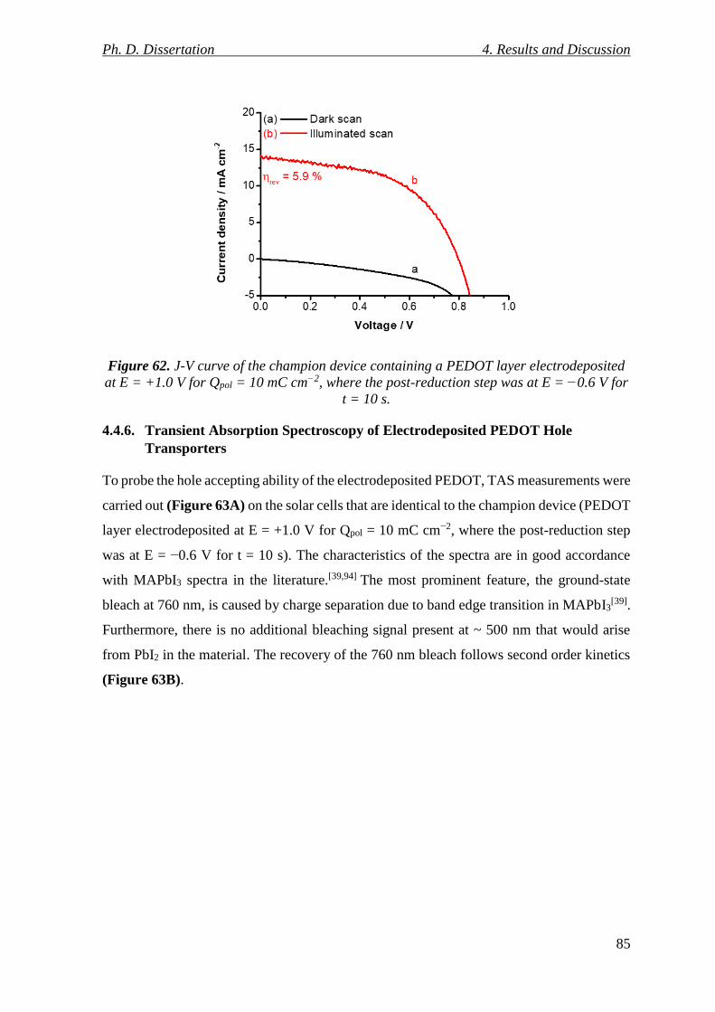
Ph. D. Dissertation 4. Results and Discussion
85
Figure 62. J-V curve of the champion device containing a PEDOT layer electrodeposited
at E = +1.0 V for Qpol = 10 mC cm−2, where the post-reduction step was at E = −0.6 V for
t = 10 s.
4.4.6. Transient Absorption Spectroscopy of Electrodeposited PEDOT Hole
Transporters
To probe the hole accepting ability of the electrodeposited PEDOT, TAS measurements were
carried out (Figure 63A) on the solar cells that are identical to the champion device (PEDOT
layer electrodeposited at E = +1.0 V for Qpol = 10 mC cm−2, where the post-reduction step
was at E = −0.6 V for t = 10 s). The characteristics of the spectra are in good accordance
with MAPbI3 spectra in the literature.[39,94] The most prominent feature, the ground-state
bleach at 760 nm, is caused by charge separation due to band edge transition in MAPbI3[39].
Furthermore, there is no additional bleaching signal present at ~ 500 nm that would arise
from PbI2 in the material. The recovery of the 760 nm bleach follows second order kinetics
(Figure 63B).
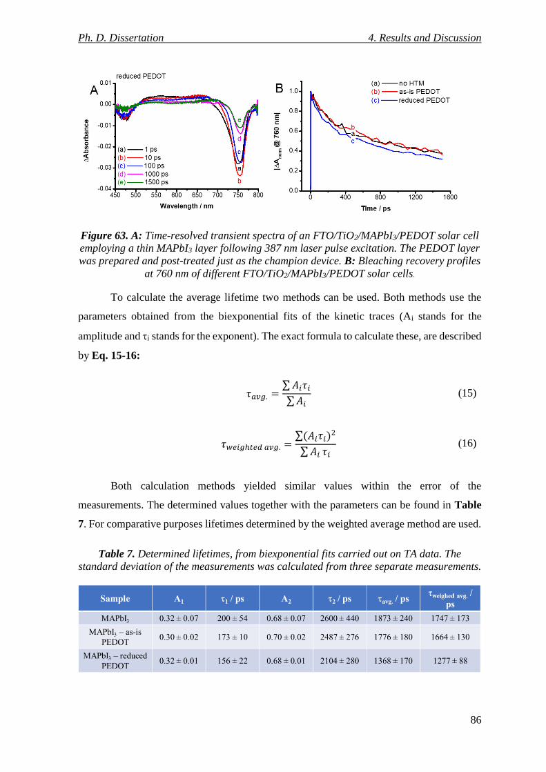
Ph. D. Dissertation 4. Results and Discussion
86
Figure 63. A: Time-resolved transient spectra of an FTO/TiO2/MAPbI3/PEDOT solar cell
employing a thin MAPbI3 layer following 387 nm laser pulse excitation. The PEDOT layer
was prepared and post-treated just as the champion device. B: Bleaching recovery profiles
at 760 nm of different FTO/TiO2/MAPbI3/PEDOT solar cells.
To calculate the average lifetime two methods can be used. Both methods use the
parameters obtained from the biexponential fits of the kinetic traces (Ai stands for the
amplitude and i stands for the exponent). The exact formula to calculate these, are described
by Eq. 15-16:
𝜏𝑎𝑣𝑔. =∑𝐴𝑖𝜏𝑖∑𝐴𝑖
(15)
𝜏𝑤𝑒𝑖𝑔ℎ𝑡𝑒𝑑 𝑎𝑣𝑔. =∑(𝐴𝑖𝜏𝑖)
2
∑𝐴𝑖 𝜏𝑖 (16)
Both calculation methods yielded similar values within the error of the
measurements. The determined values together with the parameters can be found in Table
7. For comparative purposes lifetimes determined by the weighted average method are used.
Table 7. Determined lifetimes, from biexponential fits carried out on TA data. The
standard deviation of the measurements was calculated from three separate measurements.

Ph. D. Dissertation 4. Results and Discussion
87
Fitting the data to a bi-exponential decay reveals that the average lifetime in solar
cells with different HTLs has the following trend: reduced PEDOT (tavg = 1280 ps) < as-is
PEDOT (tav = 1660 ps) < no HTM (tavg = 1750 ps). This indicates that the PEDOT layer
readily accepts holes from MAPbI3 furthermore, reducing the doping level of PEDOT
through the post-synthetic reduction technique is a viable strategy to improve the hole
accepting properties of the material.
Ph. D. Dissertation 5. Summary
88
5. Summary
Electrochemistry can be a viable tool to probe the optoelectronic properties of HOIPs.
Furthermore, sophisticated electrochemical synthesis techniques are yet to be utilized in
device fabrication. A major bottleneck in the application of HOIPs in these electrochemical
scenarios is their extreme sensitivity. Our first goal was to establish a guideline on how to
perform electrochemical experiments to obtain reliable data. As a next step we built on the
gathered experiences and aimed to unravel the effect of the ETL on the charge separation
process. For this purpose, a unique coupled technique, ultrafast transient
spectroelectrochemistry was used for the first time. To study the interaction of light with
mixed-halide PSCs, we investigated the effect of phase segregation of mixed halide solar
cells on their electronic properties. We also investigated the possibility of electrosynthesis
techniques on the preparation of a PEDOT HTL in MAPbI3 electrodes, thus forming a
regular n-i-p junction solar cell.
The most important results of the dissertation can be summarized in the following points:
1. Electrodes were prepared from two different lead halide perovskites (CsPbBr3 and
MAPbI3) by spin-coating method. Steady-state UV-vis measurements were used to
evaluate the stability of the perovskite layers in different DCM-based electrolytes. It
was found that the speed of dissolution depends on the used anion and follows the
following trend: BF4− > ClO4
− >> PF6−. Thus, electrochemical experiments can be
safely performed in Bu4NPF6/DCM electrolyte, because even after 2 hours no sign
of substantial degradation was observed. To determine the electrochemical stability
window of the layers spectroelectrochemical experiments were carried out. Multiple
redox events were observed, and a −1.0 V – +0.6 V vs Ag/AgCl for CsPbBr3 and
−0.65 V – +0.55 V vs Ag/AgCl for MAPbI3 stability window was determined.
2. To understand the exact mechanism of the potential induced degradation of the
CsPbBr3 layers we investigated the chemical changes during the anodic and cathodic
redox waves. XPS measurements revealed that during oxidation the CsPF6 is formed
on the electrode surface, parallel to the degradation of the perovskite structure. This
degradation is accompanied by a morphological change in the layers. The formation
of rectangular particles can be observed on the surface, together with the partial
dissolution of the layers (through the leaching of Pb2+ and Br−). During reduction,
the formation of Pb was observed. It was found that Pb is partially re-oxidized to
Ph. D. Dissertation 5. Summary
89
PbO upon air exposure. The morphology of the electrodes was also heavily impacted,
as the degradation was severe enough to expose the underlying TiO2 layer.
Furthermore, the formation of dendritic structures was also seen on certain parts of
the electrodes. No major change in morphology or composition was observed within
the previously proposed stability regime.
3. We combined electrochemistry and TAS to evaluate the effect of external bias on the
charge carrier recombination processes. FTO/TiO2/CsPbBr3 electrodes were
fabricated. At 0.0 V and more negative potentials the rate constant of charge carrier
recombination showed small variation. On the other hand, at more positive
potentials, a faster decay kinetics was observed. Since electrons are depleted from
the TiO2 layer under anodic bias, photogenerated electrons in CsPbBr3 are injected
into the TiO2 film. This competing charge injection process resulted in faster
bleaching recovery at anodic bias.
4. We unraveled the effect of the substrate (ETL) on the charge recombination
processes in CsPbBr3 films. In situ ultrafast transient spectroelectrochemical
experiments were carried out with FTO/CsPbBr3 electrodes (i.e., without TiO2 layer).
We found that the bleaching recovery was not influenced by the applied
electrochemical bias (within the studied time-range). These results further elucidate
the role of TiO2 in influencing the charge carrier recombination processes in
perovskite films
5. We studied the effect of light-induced phase segregation on the optical and electronic
properties of MAPbBr1.5I1.5 solar cells. Steady state UV-vis absorption spectroscopy
was used to evaluate the segregation process. After 30 minutes of white light
illumination a decrease in absorbance at 620 nm was observed which suggests the
disappearance of the mixed halide phase. Simultaneously, a concurrent increase in
the absorption at shorter and longer wavelength was observed that represents the
formation of bromide rich and iodide rich phases. This segregation process has a
marked impact on the IPCE of the devices. It was found that inducing segregation a
50 % drop in the IPCE can be observed, which detrimentally affects the performance
of such solar cells.
6. When the solar cells are stored in the dark the absorbance completely recovers,
within three hours. We found that the recovery of the IPCE is a much slower process
and it can take up to 36 hours, but it is almost completely reversible (~90 %
recovery). The slower recovery of the electronic properties suggests that charge
Ph. D. Dissertation 5. Summary
90
carrier extraction from the devices is hindered. This was attributed to the lingering
effect of the formed residual traps during phase segregation in the devices.
7. Electrochemical polymerization methods were employed to deposit PEDOT HTL on
MAPbI3 electrodes, thus forming a regular n-i-p junction solar cell. By using bis-
EDOT as the monomer, the conservation of the MAPbI3 layer was ensured.
Potentiostatic electrodeposition resulted in HTLs with controlled thicknesses. We
demonstrated that by controlling the polymerization charge density the thickness of
the PEDOT layer can be fine-tuned.
8. To improve the efficiency of the prepared solar cells, electrochemical post-treatment
techniques were used. We found that the reduction of the PEDOT layer can improve
the VOC of the devices. However, this post-reduction step has an unintended side
effect, and the MAPbI3 layer can be degraded. Three milder post-reduction
techniques were proposed. Because of the milder reduction a champion device with
a power conversion efficiency of 5.9 % was achieved. We carried out femtosecond
TAS measurements on the champion architecture. These studies revealed that
electrodeposited PEDOT is indeed an effective HTM for PSCs.
Ph. D. Dissertation 6. Összefoglalás
91
6. Összefoglalás
Az elektrokémiai módszerek egyrészt fontos eszközei lehetnek a hibrid szerves-szervetlen
perovszkitok optoelektronikai sajátságainak feltárásához, másrészt e módszerek szintézis
céljából történő felhasználása is sok lehetőséget rejt magában. A legnagyobb hátráltató
tényező a hibrid szerves-szervetlen perovszkitok környezeti hatásokkal szembeni
érzékenysége. Ezért célul tűztük ki, egy olyan körülményrendszer kidolgozását, mely
betartása mellett megbízható elektrokémiai mérések végezhetők ezen az érzékeny
anyagcsaládon. Ezen tapasztalatokat felhasználva az elektrontranszport-réteg a töltés
szétválasztási lépésben betöltött szerepét vizsgáltuk. Ezt egy egyedi csatolt technika
fejlesztésével (ultragyors tranziens spektroelektrokémia) hajtottuk végre. Ahhoz, hogy
vizsgáljuk a megvilágítás hatását is, tanulmányoztuk a fázisszeparáció hatását vegyes
halogenidtartalmú perovszkit napelemek elektronikus sajátságaira. Továbbá elektrokémiai
módszerek segítségével PEDOT lyukvezető réteget választottunk le MAPbI3 elektródokra,
ezáltal kialakítva n-i-p típusú napelemeket.
A munka tudományos tartalma összefoglalható az alábbi pontokban:
1. A doktori munkám során elvégeztem különböző ólom-halogenid tartalmú perovszkit
elektródok (CsPbBr3 és MAPbI3) előállítását forgótárcsás rétegképzés segítségével.
UV-látható spektroszkópiás mérések segítségével megvizsgáltuk ezen elektródok
stabilitását különböző diklórmetán alapú (DCM) elektrolit oldatokban.
Megállapítottuk, hogy a perovszkit rétegek leoldódásának sebessége függ a használt
anion minőségétől és az alábbi trendet követi: BF4− > ClO4
− >> PF6−. Így
bebizonyítottuk, hogy elektrokémiai mérések biztonsággal végezhetők
Bu4NPF6/DCM elektrolitban, ugyanis ebben a közegben 2 óra után sem következik
be jelentős degradáció. Ezt követően az elektrokémiai stabilitási potenciáltartomány
meghatározását tűztük ki célul, melyet spektroelektrokémiai vizsgálatokkal
végeztünk. A vizsgált potenciáltartományban több redoxi eseményt azonosítottunk,
és a CsPbBr3 rétegek esetén a −1.0 V – +0.6 V vs. Ag/AgCl illetve a MAPbI3 rétegek
esetén a −0.65 V – +0.55 V vs. Ag/AgCl stabilitási tartományt határoztuk meg.
2. Azért, hogy feltárjuk a potenciál okozta degradáció mechanizmusát, követtük a
CsPbBr3 rétegekben bekövetkező kémiai változásokat az anódos és katódos
félciklusok során. XPS vizsgálatokkal bebizonyítottuk, hogy a rétegek oxidációja
során CsPF6 képződik az elektródok felületén. Ezen felül megállapítottuk, hogy az

Ph. D. Dissertation 6. Összefoglalás
92
összetételbéli változásokhoz morfológiai változások is társulnak. Az elektródok
felületén téglatest alakú részecskék képződését figyeltük meg, miközben a rétegek
leoldódását tapasztaltuk (Pb2+ és Br− formájában). A rétegek redukciója során fém
ólom megjelenését figyeltük meg. A Pb egy része viszont PbO-á oxidálódik a
levegővel történő érintkezés során. A rétegek morfológiája ebben az esetben is
jelentősen változott. A degradáció a redukciós esetben olyan mértékű volt, hogy a
TiO2 alapréteg is láthatóvá vált. Ezen felül pedig dendritek megjelenését is
tapasztaltuk. Amennyiben viszont a javasolt potenciáltartományon belül végezzük
vizsgálatainkat, akkor a rétegek kémiai összetételében és morfológiájában csak
csekély változás volt tapasztalható.
3. Miután megállapítottuk a CsPbBr3 elektródokra jellemző elektrokémiai stabilitási
potenciáltartományt, megvizsgáltuk a külső potenciál hatását a rétegekben zajló
rekombinációs folyamatokra. Ehhez elektrokémiai és tranziens abszorpciós
technikák kombinálását valósítottuk meg. 0.0 V-nál negatívabb potenciálokon a
töltéshordozók rekombinációjára jellemző sebességi együttható értékében nem
tapasztaltunk jelentős változást. Azonban 0.0 V-nál pozitívabb esetekben a folyamat
kinetikájának felgyorsulása volt megfigyelhető. Ezt azzal magyaráztuk, hogy anódos
potenciál használata esetén a TiO2 réteg elszegényedik elektronokban, ezért a
CsPbBr3 rétegekben generált töltéshordozók számára egy új út nyílik meg. Ez a
töltés-injektálási folyamat a TiO2 réteg irányába verseng a rekombinációs
folyamattal, ezért tapasztaltuk az excitonhoz rendelhető elnyelés gyorsabb
visszaállását.
4. Megvizsgáltuk az elektronvezető-réteg hatását a CsPbBr3 rétegekben bekövetkező
rekombinációs folyamatokra. Ehhez FTO/CsPbBr3 rétegeken (a TiO2 alapréteg
elhagyásával) ultragyors spektroelektrokémiai vizsgálatokat végeztünk. Ebben az
esetben azt állapítottuk meg, hogy az alkalmazott potenciál nincs hatással az
excitonokhoz rendelhető elnyelés visszaállásának sebességére (legalábbis az általunk
vizsgált időtartományban). Ezek az eredmények további bizonyítékul szolgálnak a
TiO2 részvételére a CsPbBr3 rétegekben bekövetkező töltésrekombinációs
folyamatokban.
5. Tanulmányoztuk a fény hatására bekövetkező fázisszeparáció hatását a
MAPbBr1.5I1.5 napelemek optikai és elektromos sajátságaira. UV-látható
spektrofotometria segítségével vizsgáltuk a fázisszeparációt. 30 perc fehér fénnyel
történő megvilágítás után a napelemek fényelnyelésében 620 nm-nél csökkenést
Ph. D. Dissertation 6. Összefoglalás
93
tapasztaltunk, mely a vegyes halogenid-tartalmú fázis mennyiségének csökkenésével
magyarázható. Ezzel egyidőben, rövidebb és hosszabb hullámhosszokon egyaránt
abszorbancia növekedést tapasztaltunk, mely a bromid- és jodid-gazdag fázisok
megjelenését bizonyítja. Ez a fázisszeparációs folyamat hatással van a napelemek
IPCE görbéjére is. A szeparációt követően ugyanis 50 % csökkenést tapasztaltunk az
IPCE értékekben, mely fázisszeparáción átesett napelemek hatékonyságában is
megmutatkozik.
6. A napelemek sötétben való tárolását követően, azok optikai sajátságai 3 órát
követően teljesen regenerálódnak. Azt tapasztaltuk, hogy az IPCE értékek
visszaállása egy sokkal időigényesebb folyamat, ami akár 36 órát is igénybe vehet.
Ennek ellenére a folyamat közel reverzibilisnek tekinthető (~90 %-os regenerálódás).
Az elektromos sajátságok lassabb visszaállásából azt a következtetést vontuk le,
hogy a töltéshordozók kinyerése válik gátolt folyamattá a napelemekben, amely a
perovszkit rétegekben kialakuló hibahelyek lassú eltűnésével magyarázható.
7. Elektrokémiai polimerizáció segítségével sikeresen választottunk le PEDOT
lyukvezető réteget MAPbI3 elektródok felületére, ezzel kialakítva egy n-i-p típusú
napelemet. A MAPbI3 réteg degradációjának elkerülése végett, az elektrokémiai
leválasztás során bis-EDOT monomert használtunk. Potenciosztatikus leválasztás
alkalmazásával sikeresen szabályoztuk a PEDOT lyukvezető réteg vastagságát.
8. Elektrokémiai utókezelések használatával kívántuk a PEDOT lyukvezető réteget
tartalmazó napelemek hatékonyságát növelni. A napelemek VOC értékében érdemi
javulást tudtunk előidézni a PEDOT rétegek elektroredukciójával. Azonban ennek
az utókezelésnek nem kívánt mellékhatásaként a MAPbI3 rétegek degradációját
tapasztaltuk. Három enyhébb utóredukciós kezelést vizsgáltunk meg. Ennek
köszönhetően a legjobb teljesítményű napelem hatékonysága elérte az 5.8 %-ot.
Femtoszekundumos tranziens abszorpciós spektroszkópia segítségével
megállapítottuk, hogy a PEDOT réteg képes hatékony lyukvezető rétegként
funkcionálni.
.
Ph. D. Dissertation 7. References
94
7. References
[1] W.S. Yang, B.-W. Park, E.H. Jung, N.J. Jeon, Y.C. Kim, D.U. Lee, S.S. Shin, J. Seo, E.K. Kim, J.H.
Noh, S. Il Seok, Iodide Management in Formamidinium-Lead-Halide–Based Perovskite Layers for
Efficient Solar Cells, Science 356 (2017) 1376–1379.
[2] Y. Yang, M. Yang, K. Zhu, J.C. Johnson, J.J. Berry, J. van de Lagemaat, M.C. Beard, Large
Polarization-Dependent Exciton Optical Stark Effect in Lead Iodide Perovskites, Nat. Commun. 7
(2016) 12613.
[3] Z.-K. Tan, R.S. Moghaddam, M.L. Lai, P. Docampo, R. Higler, F. Deschler, M. Price, A. Sadhanala,
L.M. Pazos, D. Credgington, F. Hanusch, T. Bein, H.J. Snaith, R.H. Friend, Bright Light-Emitting
Diodes Based on Organometal Halide Perovskite, Nat. Nanotechnol. 9 (2014) 687–692.
[4] S.A. Veldhuis, P.P. Boix, N. Yantara, M. Li, T.C. Sum, N. Mathews, S.G. Mhaisalkar, Perovskite
Materials for Light-Emitting Diodes and Lasers, Adv. Mater. 28 (2016) 6804–6834.
[5] H. Wang, D.H. Kim, Perovskite-Based Photodetectors: Materials and Devices, Chem. Soc. Rev. 46
(2017) 5204–5236.
[6] M. Ahmadi, T. Wu, B. Hu, A Review on Organic-Inorganic Halide Perovskite Photodetectors: Device
Engineering and Fundamental Physics, Adv. Mater. 29 (2017) 1605242.
[7] B. Yang, F. Zhang, J. Chen, S. Yang, X. Xia, T. Pullerits, W. Deng, K. Han, Ultrasensitive and Fast
All-Inorganic Perovskite-Based Photodetector via Fast Carrier Diffusion, Adv. Mater. 29 (2017)
1703758.
[8] S. Yakunin, M. Sytnyk, D. Kriegner, S. Shrestha, M. Richter, G.J. Matt, H. Azimi, C.J. Brabec, J.
Stangl, M. V. Kovalenko, W. Heiss, Detection of X-ray Photons by Solution-Processed Lead Halide
Perovskites, Nat. Photonics. 9 (2015) 444–449.
[9] S. Yakunin, D.N. Dirin, Y. Shynkarenko, V. Morad, I. Cherniukh, O. Nazarenko, D. Kreil, T. Nauser,
M. V. Kovalenko, Detection of Gamma Photons Using Solution-Grown Single Crystals of Hybrid Lead
Halide Perovskites, Nat. Photonics. 10 (2016) 585–589.
[10] V.M. Goldschmidt, Die Gesetze der Krystallochemie, Naturwissenschaften. 14 (1926) 477–485.
[11] A.M. Glazer, The Classification of Tilted Octahedra in Perovskites, Acta Crystallogr. Sect. B Struct.
Crystallogr. Cryst. Chem. 28 (1972) 3384–3392.
[12] D.B. Mitzi, Templating and Structural Engineering in Organic–Inorganic Perovskites, J. Chem. Soc.
Dalt. Trans. 0 (2001) 1–12.
[13] B. Saparov, D.B. Mitzi, Organic–Inorganic Perovskites: Structural Versatility for Functional
Materials Design, Chem. Rev. 116 (2016) 4558–4596.
[14] Y. Chen, Y. Sun, J. Peng, W. Zhang, X. Su, K. Zheng, T. Pullerits, Z. Liang, Tailoring Organic Cation
of 2D Air-Stable Organometal Halide Perovskites for Highly Efficient Planar Solar Cells, Adv. Energy
Mater. 7 (2017) 1700162.
[15] L. Liang, L. Wencong, C. Nianyi, On the Criteria of Formation and Lattice Distortion of Perovskite-
Type Complex Halides, J. Phys. Chem. Solids. 65 (2004) 855–860.
[16] C. Li, X. Lu, W. Ding, L. Feng, Y. Gao, Z. Guo, Formability of ABX3 ( X = F, Cl, Br, I) Halide
Perovskites, Acta Crystallogr. Sect. B Struct. Sci. 64 (2008) 702–707.
[17] G. Kieslich, S. Sun, A.K. Cheetham, Solid-State Principles Applied to Organic–Inorganic Perovskites:
New Tricks for an Old Dog, Chem. Sci. 5 (2014) 4712–4715.
[18] G. Kieslich, S. Sun, A.K. Cheetham, An Extended Tolerance Factor Approach for Organic–Inorganic
Perovskites, Chem. Sci. 6 (2015) 3430–3433.
[19] J.S. Manser, J.A. Christians, P. V. Kamat, Intriguing Optoelectronic Properties of Metal Halide
Perovskites, Chem. Rev. 116 (2016) 12956–13008.
[20] J.D. Donaldson, J. Silver, S. Hadjiminolis, S.D. Ross, Effects of the Presence of Valence-Shell Non-
Bonding Electron Pairs on the Properties and Structures of Caesium Tin(II) Bromides and of Related
Antimony and Tellurium Compounds, J. Chem. Soc. Dalt. Trans. 0 (1975) 1500-1506.
[21] R.J. Worhatch, H. Kim, I.P. Swainson, A.L. Yonkeu, S.J.L. Billinge, Study of Local Structure in
Selected Organic–Inorganic Perovskites in the Pm3m Phase, Chem. Mater. 20 (2008) 1272–1277.
[22] I. Swainson, L. Chi, J.-H. Her, L. Cranswick, P. Stephens, B. Winkler, D.J. Wilson, V. Milman,
Orientational Ordering, Tilting and Lone-Pair Activity in the Perovskite Methylammonium Tin
Bromide, CH3NH3SnBr3, Acta Crystallogr. Sect. B Struct. Sci. 66 (2010) 422–429.
[23] T. Mizokawa, Jahn-Teller Effects in Transition-Metal Compounds with Small Charge-Transfer
Energy, J. Phys. Conf. Ser. 428 (2013) 12020.
[24] N. Matsushita, H. Kitagawa, N. Kojima, A Three-Dimensional Iodo-Bridged Mixed-Valence Gold(I,
III) Compound, Cs2Au(I)Au(III)I6, Acta Crystallogr. Sect. C Cryst. Struct. Commun. 53 (1997) 663–
666.
Ph. D. Dissertation 7. References
95
[25] N. Elliott, L. Pauling, The Crystal Structure of Cesium Aurous Auric Chloride, Cs2AuAuCl6, and
Cesium Argentous Auric Chloride, Cs2AgAuCl6, J. Am. Chem. Soc. 60 (1938) 1846–1851.
[26] T. Jeon, S.J. Kim, J. Yoon, J. Byun, H.R. Hong, T.-W. Lee, J.-S. Kim, B. Shin, S.O. Kim, Hybrid
Perovskites: Effective Crystal Growth for Optoelectronic Applications, Adv. Energy Mater. 7 (2017)
1602596.
[27] H.-B. Kim, H. Choi, J. Jeong, S. Kim, B. Walker, S. Song, J.Y. Kim, Mixed Solvents for the
Optimization of Morphology in Solution-Processed, Inverted-Type Perovskite/Fullerene Hybrid Solar
Cells, Nanoscale. 6 (2014) 6679-6683.
[28] D.P. Nenon, J.A. Christians, L.M. Wheeler, J.L. Blackburn, E.M. Sanehira, B. Dou, M.L. Olsen, K.
Zhu, J.J. Berry, J.M. Luther, Structural and Chemical Evolution of Methylammonium Lead Halide
Perovskites During Thermal Processing From Solution, Energy Environ. Sci. 9 (2016) 2072–2082.
[29] J.S. Manser, B. Reid, P. V. Kamat, Evolution of Organic–Inorganic Lead Halide Perovskite from
Solid-State Iodoplumbate Complexes, J. Phys. Chem. C. 119 (2015) 17065–17073.
[30] G.E. Eperon, V.M. Burlakov, P. Docampo, A. Goriely, H.J. Snaith, Morphological Control for High
Performance, Solution-Processed Planar Heterojunction Perovskite Solar Cells, Adv. Funct. Mater.
24 (2014) 151–157.
[31] G. Grancini, S. Marras, M. Prato, C. Giannini, C. Quarti, F. De Angelis, M. De Bastiani, G.E. Eperon,
H.J. Snaith, L. Manna, A. Petrozza, The Impact of the Crystallization Processes on the Structural and
Optical Properties of Hybrid Perovskite Films for Photovoltaics, J. Phys. Chem. Lett. 5 (2014) 3836–
3842.
[32] M. Liu, M.B. Johnston, H.J. Snaith, Efficient Planar Heterojunction Perovskite Solar Cells by Vapour
Deposition, Nature. 501 (2013) 395–398.
[33] N.J. Jeon, J.H. Noh, Y.C. Kim, W.S. Yang, S. Ryu, S. Il Seok, Solvent Engineering for High-
Performance Inorganic–Organic Hybrid Perovskite Solar Cells, Nat. Mater. 13 (2014) 897–903.
[34] M. Xiao, F. Huang, W. Huang, Y. Dkhissi, Y. Zhu, J. Etheridge, A. Gray-Weale, U. Bach, Y.-B. Cheng,
L. Spiccia, A Fast Deposition-Crystallization Procedure for Highly Efficient Lead Iodide Perovskite
Thin-Film Solar Cells, Angew. Chemie. 126 (2014) 10056–10061.
[35] S. Paek, P. Schouwink, E.N. Athanasopoulou, K.T. Cho, G. Grancini, Y. Lee, Y. Zhang, F. Stellacci,
M.K. Nazeeruddin, P. Gao, From Nano- to Micrometer Scale: The Role of Antisolvent Treatment on
High Performance Perovskite Solar Cells, Chem. Mater. 29 (2017) 3490–3498.
[36] H. Yu, F. Wang, F. Xie, W. Li, J. Chen, N. Zhao, The Role of Chlorine in the Formation Process of
“CH3NH3PbI3-xClx” Perovskite, Adv. Funct. Mater. (2014) 7102–7108
[37] S. Colella, E. Mosconi, P. Fedeli, A. Listorti, F. Gazza, F. Orlandi, P. Ferro, T. Besagni, A. Rizzo, G.
Calestani, G. Gigli, F. De Angelis, R. Mosca, MAPbI3-xClx Mixed Halide Perovskite for Hybrid Solar
Cells: The Role of Chloride as Dopant on the Transport and Structural Properties, Chem. Mater. 25
(2013) 4613–4618.
[38] B. Li, C. Fei, K. Zheng, X. Qu, T. Pullerits, G. Cao, J. Tian, Constructing Water-Resistant CH3NH3PbI3
Perovskite Films via Coordination Interaction, J. Mater. Chem. A. 4 (2016) 17018–17024.
[39] K.G. Stamplecoskie, J.S. Manser, P. V. Kamat, Dual Nature of the Excited State in Organic–Inorganic
Lead Halide Perovskites, Energy Environ. Sci. 8 (2015) 208–215.
[40] N. Ahn, D.-Y. Son, I.-H. Jang, S.M. Kang, M. Choi, N.-G. Park, Highly Reproducible Perovskite Solar
Cells with Average Efficiency of 18.3% and Best Efficiency of 19.7% Fabricated via Lewis Base Adduct
of Lead(II) Iodide, J. Am. Chem. Soc. 137 (2015) 8696–8699.
[41] J.S. Manser, M.I. Saidaminov, J.A. Christians, O.M. Bakr, P. V. Kamat, Making and Breaking of Lead
Halide Perovskites, Acc. Chem. Res. 49 (2016) 330–338.
[42] Y. Guo, K. Shoyama, W. Sato, Y. Matsuo, K. Inoue, K. Harano, C. Liu, H. Tanaka, E. Nakamura,
Chemical Pathways Connecting Lead(II) Iodide and Perovskite via Polymeric Plumbate(II) Fiber, J.
Am. Chem. Soc. 137 (2015) 15907–15914.
[43] D.T. Moore, H. Sai, K.W. Tan, D.-M. Smilgies, W. Zhang, H.J. Snaith, U. Wiesner, L.A. Estroff,
Crystallization Kinetics of Organic–Inorganic Trihalide Perovskites and the Role of the Lead Anion in
Crystal Growth, J. Am. Chem. Soc. 137 (2015) 2350–2358.
[44] K. Liang, D.B. Mitzi, M.T. Prikas, Synthesis and Characterization of Organic−Inorganic Perovskite
Thin Films Prepared Using a Versatile Two-Step Dipping Technique, Chem. Mater. 10 (1998) 403–
411.
[45] J. Burschka, N. Pellet, S.-J. Moon, R. Humphry-Baker, P. Gao, M.K. Nazeeruddin, M. Grätzel,
Sequential Deposition as a Route to High-Performance Perovskite-Sensitized Solar Cells, Nature. 499
(2013) 316–319.
[46] Z. Xiao, C. Bi, Y. Shao, Q. Dong, Q. Wang, Y. Yuan, C. Wang, Y. Gao, J. Huang, Efficient, High Yield
Perovskite Photovoltaic Devices Grown by Interdiffusion of Solution-Processed Precursor Stacking
Layers, Energy Environ. Sci. 7 (2014) 2619–2623.
Ph. D. Dissertation 7. References
96
[47] L.K. Ono, M.R. Leyden, S. Wang, Y. Qi, Organometal Halide Perovskite Thin Films and Solar Cells
by Vapor Deposition, J. Mater. Chem. A. 4 (2016) 6693–6713.
[48] D. Forgács, L. Gil-Escrig, D. Pérez-Del-Rey, C. Momblona, J. Werner, B. Niesen, C. Ballif, M.
Sessolo, H.J. Bolink, Efficient Monolithic Perovskite/Perovskite Tandem Solar Cells, Adv. Energy
Mater. 7 (2017) 1602121.
[49] D. Shi, V. Adinolfi, R. Comin, M. Yuan, E. Alarousu, A. Buin, Y. Chen, S. Hoogland, A.
Rothenberger, K. Katsiev, Y. Losovyj, X. Zhang, P.A. Dowben, O.F. Mohammed, E.H. Sargent, O.M.
Bakr, Low Trap-State Density and Long Carrier Diffusion in Organolead Trihalide Perovskite Single
Crystals, Science 347 (2015) 519–522.
[50] Y. Dang, Y. Liu, Y. Sun, D. Yuan, X. Liu, W. Lu, G. Liu, H. Xia, X. Tao, Bulk Crystal Growth of
Hybrid Perovskite Material CH3NH3PbI3, CrystEngComm. 17 (2015) 665–670.
[51] M.I. Saidaminov, A.L. Abdelhady, B. Murali, E. Alarousu, V.M. Burlakov, W. Peng, I. Dursun, L.
Wang, Y. He, G. Maculan, A. Goriely, T. Wu, O.F. Mohammed, O.M. Bakr, High-Quality Bulk Hybrid
Perovskite Single Crystals Within Minutes by Inverse Temperature Crystallization, Nat. Commun. 6
(2015) 7586.
[52] G. Maculan, A.D. Sheikh, A.L. Abdelhady, M.I. Saidaminov, M.A. Haque, B. Murali, E. Alarousu,
O.F. Mohammed, T. Wu, O.M. Bakr, CH3NH3PbCl3 Single Crystals: Inverse Temperature
Crystallization and Visible-Blind UV-Photodetector, J. Phys. Chem. Lett. 6 (2015) 3781–3786.
[53] M.I. Saidaminov, A.L. Abdelhady, G. Maculan, O.M. Bakr, Retrograde Solubility of Formamidinium
and Methylammonium Lead Halide Perovskites Enabling Rapid Single Crystal Growth, Chem.
Commun. 51 (2015) 17658–17661.
[54] F. Brivio, K.T. Butler, A. Walsh, M. van Schilfgaarde, Relativistic Quasiparticle Self-Consistent
Electronic Structure of Hybrid Halide Perovskite Photovoltaic Absorbers, Phys. Rev. B. 89 (2014)
155204.
[55] P. Umari, E. Mosconi, F. De Angelis, Relativistic GW Calculations on CH3NH3PbI3 and CH3NH3SnI3
Perovskites for Solar Cell Applications, Sci. Rep. 4 (2015) 4467.
[56] A. Miyata, A. Mitioglu, P. Plochocka, O. Portugall, J.T.-W. Wang, S.D. Stranks, H.J. Snaith, R.J.
Nicholas, Direct Measurement of the Exciton Binding Energy and Effective Masses for Charge
Carriers in Organic–Inorganic Trihalide Perovskites, Nat. Phys. 11 (2015) 582–587.
[57] J. Huang, Y. Yuan, Y. Shao, Y. Yan, Understanding the Physical Properties of Hybrid Perovskites for
Photovoltaic Applications, Nat. Rev. Mater. 2 (2017) 17042.
[58] W.-J. Yin, T. Shi, Y. Yan, Unique Properties of Halide Perovskites as Possible Origins of the Superior
Solar Cell Performance, Adv. Mater. 26 (2014) 4653–4658.
[59] N. Jensen, U. Rau, R.M. Hausner, S. Uppal, L. Oberbeck, R.B. Bergmann, J.H. Werner, Recombination
Mechanisms in Amorphous Silicon/Crystalline Silicon Heterojunction Solar Cells, J. Appl. Phys. 87
(2000) 2639–2645.
[60] S. De Wolf, J. Holovsky, S.-J. Moon, P. Löper, B. Niesen, M. Ledinsky, F.-J. Haug, J.-H. Yum, C.
Ballif, Organometallic Halide Perovskites: Sharp Optical Absorption Edge and Its Relation to
Photovoltaic Performance, J. Phys. Chem. Lett. 5 (2014) 1035–1039.
[61] D.P. McMeekin, G. Sadoughi, W. Rehman, G.E. Eperon, M. Saliba, M.T. Horantner, A. Haghighirad,
N. Sakai, L. Korte, B. Rech, M.B. Johnston, L.M. Herz, H.J. Snaith, A Mixed-Cation Lead Mixed-
Halide Perovskite Absorber for Tandem Solar Cells, Science 351 (2016) 151–155.
[62] Y. Hu, E.M. Hutter, P. Rieder, I. Grill, J. Hanisch, M.F. Aygüler, A.G. Hufnagel, M. Handloser, T.
Bein, A. Hartschuh, K. Tvingstedt, V. Dyakonov, A. Baumann, T.J. Savenije, M.L. Petrus, P.
Docampo, Understanding the Role of Cesium and Rubidium Additives in Perovskite Solar Cells: Trap
States, Charge Transport, and Recombination, Adv. Energy Mater. (2018) 1703057.
[63] T. Jesper Jacobsson, J.-P. Correa-Baena, M. Pazoki, M. Saliba, K. Schenk, M. Grätzel, A. Hagfeldt,
Exploration of the Compositional Space for Mixed Lead Halogen Perovskites for High Efficiency Solar
Cells, Energy Environ. Sci. 9 (2016) 1706–1724.
[64] S. Sarkar, P. Mahadevan, Role of the A-site Cation in Determining the Properties of the Hybrid
Perovskite CH3NH3PbBr3, Phys. Rev. B. 95 (2017) 214118.
[65] C.W. Myung, J. Yun, G. Lee, K.S. Kim, A New Perspective on the Role of A-Site Cations in Perovskite
Solar Cells, Adv. Energy Mater. (2018) 1702898.
[66] G. Giorgi, J.-I. Fujisawa, H. Segawa, K. Yamashita, Cation Role in Structural and Electronic
Properties of 3D Organic–Inorganic Halide Perovskites: A DFT Analysis, J. Phys. Chem. C. 118
(2014) 12176–12183.
[67] A. Binek, F.C. Hanusch, P. Docampo, T. Bein, Stabilization of the Trigonal High-Temperature Phase
of Formamidinium Lead Iodide, J. Phys. Chem. Lett. 6 (2015) 1249–1253.
[68] Z. Li, M. Yang, J.-S. Park, S.-H. Wei, J.J. Berry, K. Zhu, Stabilizing Perovskite Structures by Tuning
Tolerance Factor: Formation of Formamidinium and Cesium Lead Iodide Solid-State Alloys, Chem.
Ph. D. Dissertation 7. References
97
Mater. 28 (2016) 284–292.
[69] P. Kanhere, S. Chakraborty, C.J. Rupp, R. Ahuja, Z. Chen, Substitution Induced Band Structure Shape
Tuning in Hybrid Perovskites (CH3NH3Pb1−xSnxI3) for Efficient Solar Cell Applications, RSC Adv. 5
(2015) 107497–107502.
[70] Y. Ogomi, A. Morita, S. Tsukamoto, T. Saitho, N. Fujikawa, Q. Shen, T. Toyoda, K. Yoshino, S.S.
Pandey, T. Ma, S. Hayase, CH3NH3SnxPb(1– x)I3 Perovskite Solar Cells Covering up to 1060 nm, J.
Phys. Chem. Lett. 5 (2014) 1004–1011.
[71] F. Hao, C.C. Stoumpos, R.P.H. Chang, M.G. Kanatzidis, Anomalous Band Gap Behavior in Mixed Sn
and Pb Perovskites Enables Broadening of Absorption Spectrum in Solar Cells, J. Am. Chem. Soc.
136 (2014) 8094–8099.
[72] G. Nedelcu, L. Protesescu, S. Yakunin, M.I. Bodnarchuk, M.J. Grotevent, M. V. Kovalenko, Fast
Anion-Exchange in Highly Luminescent Nanocrystals of Cesium Lead Halide Perovskites (CsPbX3 , X
= Cl, Br, I), Nano Lett. 15 (2015) 5635–5640.
[73] Q.A. Akkerman, V. D’Innocenzo, S. Accornero, A. Scarpellini, A. Petrozza, M. Prato, L. Manna,
Tuning the Optical Properties of Cesium Lead Halide Perovskite Nanocrystals by Anion Exchange
Reactions, J. Am. Chem. Soc. 137 (2015) 10276–10281.
[74] G. Li, J.Y.-L. Ho, M. Wong, H.S. Kwok, Reversible Anion Exchange Reaction in Solid Halide
Perovskites and Its Implication in Photovoltaics, J. Phys. Chem. C. 119 (2015) 26883–26888.
[75] D.M. Jang, K. Park, D.H. Kim, J. Park, F. Shojaei, H.S. Kang, J.-P. Ahn, J.W. Lee, J.K. Song,
Reversible Halide Exchange Reaction of Organometal Trihalide Perovskite Colloidal Nanocrystals for
Full-Range Band Gap Tuning, Nano Lett. 15 (2015) 5191–5199.
[76] N. Pellet, J. Teuscher, J. Maier, M. Grätzel, Transforming Hybrid Organic Inorganic Perovskites by
Rapid Halide Exchange, Chem. Mater. 27 (2015) 2181–2188.
[77] J.H. Noh, S.H. Im, J.H. Heo, T.N. Mandal, S. Il Seok, Chemical Management for Colorful, Efficient,
and Stable Inorganic–Organic Hybrid Nanostructured Solar Cells, Nano Lett. 13 (2013) 1764–1769.
[78] J.B. Hoffman, A.L. Schleper, P. V. Kamat, Transformation of Sintered CsPbBr3 Nanocrystals to Cubic
CsPbI3 and Gradient CsPbBrxI3– x through Halide Exchange, J. Am. Chem. Soc. 138 (2016) 8603–
8611.
[79] M.C. Brennan, S. Draguta, P. V. Kamat, M. Kuno, Light-Induced Anion Phase Segregation in Mixed
Halide Perovskites, ACS Energy Lett. 3 (2018) 204–213.
[80] E.T. Hoke, D.J. Slotcavage, E.R. Dohner, A.R. Bowring, H.I. Karunadasa, M.D. McGehee, Reversible
Photo-Induced Trap Formation in Mixed-Halide Hybrid Perovskites for Photovoltaics, Chem. Sci. 6
(2015) 613–617.
[81] Q. Dong, Y. Fang, Y. Shao, P. Mulligan, J. Qiu, L. Cao, J. Huang, Electron-Hole Diffusion Lengths >
175 m in Solution-Grown CH3NH3PbI3 Single Crystals, Science 347 (2015) 967–970.
[82] A. Kojima, K. Teshima, Y. Shirai, T. Miyasaka, Organometal Halide Perovskites as Visible-Light
Sensitizers for Photovoltaic Cells, J. Am. Chem. Soc. 131 (2009) 6050–6051.
[83] J.-H. Im, C.-R. Lee, J.-W. Lee, S.-W. Park, N.-G. Park, 6.5 % Efficient Perovskite Quantum-Dot-
Sensitized Solar Cell, Nanoscale. 3 (2011) 4088-4093.
[84] J.M. Ball, M.M. Lee, A. Hey, H.J. Snaith, Low-Temperature Processed Meso-Superstructured to Thin-
Film Perovskite Solar Cells, Energy Environ. Sci. 6 (2013) 1739-1743.
[85] Y. Li, S. Ye, W. Sun, W. Yan, Y. Li, Z. Bian, Z. Liu, S. Wang, C. Huang, Hole-Conductor-Free Planar
Perovskite Solar Cells with 16.0 % Efficiency, J. Mater. Chem. A. 3 (2015) 18389–18394.
[86] J. Shi, J. Dong, S. Lv, Y. Xu, L. Zhu, J. Xiao, X. Xu, H. Wu, D. Li, Y. Luo, Q. Meng, Hole-Conductor-
Free Perovskite Organic Lead Iodide Heterojunction Thin-Film Solar Cells: High Efficiency and
Junction Property, Appl. Phys. Lett. 104 (2014) 63901.
[87] V. D’Innocenzo, G. Grancini, M.J.P. Alcocer, A.R.S. Kandada, S.D. Stranks, M.M. Lee, G. Lanzani,
H.J. Snaith, A. Petrozza, Excitons Versus Free Charges in Organo-Lead Trihalide Perovskites, Nat.
Commun. 5 (2014) 1–6.
[88] K. Tanaka, T. Takahashi, T. Ban, T. Kondo, K. Uchida, N. Miura, Comparative Study on the Excitons
in Lead-Halide-Based Perovskite-Type Crystals CH3NH3PbBr3 CH3NH3PbI3, Solid State Commun.
127 (2003) 619–623.
[89] M. Hu, C. Bi, Y. Yuan, Z. Xiao, Q. Dong, Y. Shao, J. Huang, Distinct Exciton Dissociation Behavior
of Organolead Trihalide Perovskite and Excitonic Semiconductors Studied in the Same System, Small.
11 (2015) 2164–2169.
[90] T.C. Sum, N. Mathews, Advancements in Perovskite Solar Cells: Photophysics Behind the
Photovoltaics, Energy Environ. Sci. 7 (2014) 2518–2534.
[91] G. Xing, N. Mathews, S. Sun, S.S. Lim, Y.M. Lam, M. Gratzel, S. Mhaisalkar, T.C. Sum, Long-Range
Balanced Electron- and Hole-Transport Lengths in Organic-Inorganic CH3NH3PbI3, Science 342
(2013) 344–347.
Ph. D. Dissertation 7. References
98
[92] K. Zheng, Q. Zhu, M. Abdellah, M.E. Messing, W. Zhang, A. Generalov, Y. Niu, L. Ribaud, S.E.
Canton, T. Pullerits, Exciton Binding Energy and the Nature of Emissive States in Organometal Halide
Perovskites, J. Phys. Chem. Lett. 6 (2015) 2969–2975.
[93] S.D. Stranks, G.E. Eperon, G. Grancini, C. Menelaou, M.J.P. Alcocer, T. Leijtens, L.M. Herz, A.
Petrozza, H.J. Snaith, Electron-Hole Diffusion Lengths Exceeding 1 Micrometer in an Organometal
Trihalide Perovskite Absorber, Science 342 (2013) 341–344.
[94] J. Peng, Y. Chen, K. Zheng, T. Pullerits, Z. Liang, Insights Into Charge Carrier Dynamics in Organo-
Metal Halide Perovskites: From Neat Films to Solar Cells, Chem. Soc. Rev. 46 (2017) 5714–5729.
[95] K. Zheng, K. Žídek, M. Abdellah, J. Chen, P. Chábera, W. Zhang, M.J. Al-Marri, T. Pullerits, High
Excitation Intensity Opens a New Trapping Channel in Organic–Inorganic Hybrid Perovskite
Nanoparticles, ACS Energy Lett. 1 (2016) 1154–1161.
[96] J. Chen, P. Chábera, T. Pascher, M.E. Messing, R. Schaller, S. Canton, K. Zheng, T. Pullerits,
Enhanced Size Selection in Two-Photon Excitation for CsPbBr3 Perovskite Nanocrystals, J. Phys.
Chem. Lett. 8 (2017) 5119–5124.
[97] H. Huang, M.I. Bodnarchuk, S. V. Kershaw, M. V. Kovalenko, A.L. Rogach, Lead Halide Perovskite
Nanocrystals in the Research Spotlight: Stability and Defect Tolerance, ACS Energy Lett. 2 (2017)
2071–2083.
[98] K. Zheng, K. Žídek, M. Abdellah, M.E. Messing, M.J. Al-Marri, T. Pullerits, Trap States and Their
Dynamics in Organometal Halide Perovskite Nanoparticles and Bulk Crystals, J. Phys. Chem. C. 120
(2016) 3077–3084.
[99] J.M. Ball, A. Petrozza, Defects in Perovskite-Halides and Their Effects in Solar Cells, Nat. Energy. 1
(2016) 16149.
[100] D. Macdonald, A. Cuevas, Understanding Carrier Trapping in Multicrystalline Silicon, Sol. Energy
Mater. Sol. Cells. 65 (2001) 509–516.
[101] P. Parkinson, J. Lloyd-Hughes, Q. Gao, H.H. Tan, C. Jagadish, M.B. Johnston, L.M. Herz, Transient
Terahertz Conductivity of GaAs Nanowires, Nano Lett. 7 (2007) 2162–2165.
[102] P. Sasanpour, R. Mohammadpour, Trap Density Measurement in Three-Dimensional Nanostructured
Photoelectrode of Titanium Dioxide with Various Morphologies, Appl. Phys. A. 122 (2016) 476.
[103] Y. Fang, Q. Dong, Y. Shao, Y. Yuan, J. Huang, Highly Narrowband Perovskite Single-Crystal
Photodetectors Enabled by Surface-Charge Recombination, Nat. Photonics. 9 (2015) 679–686.
[104] S.Y. Leblebici, L. Leppert, Y. Li, S.E. Reyes-Lillo, S. Wickenburg, E. Wong, J. Lee, M. Melli, D.
Ziegler, D.K. Angell, D.F. Ogletree, P.D. Ashby, F.M. Toma, J.B. Neaton, I.D. Sharp, A. Weber-
Bargioni, Facet-dependent Photovoltaic Efficiency Variations in Single Grains of Hybrid Halide
Perovskite, Nat. Energy. 1 (2016) 16093.
[105] Y. Shao, Z. Xiao, C. Bi, Y. Yuan, J. Huang, Origin and Elimination of Photocurrent Hysteresis by
Fullerene Passivation in CH3NH3PbI3 Planar Heterojunction Solar Cells, Nat. Commun. 5 (2014)
5784.
[106] J.A. Christians, P.A. Miranda Herrera, P. V. Kamat, Transformation of the Excited State and
Photovoltaic Efficiency of CH3NH3PbI3 Perovskite upon Controlled Exposure to Humidified Air, J.
Am. Chem. Soc. 137 (2015) 1530–1538.
[107] J. Yang, B.D. Siempelkamp, D. Liu, T.L. Kelly, Investigation of CH3NH3PbI3 Degradation Rates and
Mechanisms in Controlled Humidity Environments Using in Situ Techniques, ACS Nano. 9 (2015)
1955–1963.
[108] A.M.A. Leguy, Y. Hu, M. Campoy-Quiles, M.I. Alonso, O.J. Weber, P. Azarhoosh, M. van
Schilfgaarde, M.T. Weller, T. Bein, J. Nelson, P. Docampo, P.R.F. Barnes, Reversible Hydration of
CH3NH3PbI3 in Films, Single Crystals, and Solar Cells, Chem. Mater. 27 (2015) 3397–3407.
[109] T.A. Berhe, W.-N. Su, C.-H. Chen, C.-J. Pan, J.-H. Cheng, H.-M. Chen, M.-C. Tsai, L.-Y. Chen, A.A.
Dubale, B.-J. Hwang, Organometal Halide Perovskite Solar Cells: Degradation and Stability, Energy
Environ. Sci. 9 (2016) 323–356.
[110] W. Huang, J.S. Manser, P. V. Kamat, S. Ptasinska, Evolution of Chemical Composition, Morphology,
and Photovoltaic Efficiency of CH3NH3PbI3 Perovskite under Ambient Conditions, Chem. Mater. 28
(2016) 303–311.
[111] Y. Zhao, K. Zhu, Optical Bleaching of Perovskite (CH3NH3)PbI3 Through Room-Temperature Phase
Transformation Induced by Ammonia, Chem. Commun. 50 (2014) 1605-1607.
[112] N. Aristidou, I. Sanchez-Molina, T. Chotchuangchutchaval, M. Brown, L. Martinez, T. Rath, S.A.
Haque, The Role of Oxygen in the Degradation of Methylammonium Lead Trihalide Perovskite
Photoactive Layers, Angew. Chemie Int. Ed. 54 (2015) 8208–8212.
[113] D. Bryant, N. Aristidou, S. Pont, I. Sanchez-Molina, T. Chotchunangatchaval, S. Wheeler, J.R.
Durrant, S.A. Haque, Light and Oxygen Induced Degradation Limits the Operational Stability of
Methylammonium Lead Triiodide Perovskite Solar Cells, Energy Environ. Sci. 9 (2016) 1655–1660.
Ph. D. Dissertation 7. References
99
[114] F.T.F. O’Mahony, Y.H. Lee, C. Jellett, S. Dmitrov, D.T.J. Bryant, J.R. Durrant, B.C. O’Regan, M.
Graetzel, M.K. Nazeeruddin, S.A. Haque, Improved Environmental Stability of Organic Lead
Trihalide Perovskite-Based Photoactive-Layers in the Presence of Mesoporous TiO2, J. Mater. Chem.
A. 3 (2015) 7219–7223.
[115] J. Yang, T.L. Kelly, Decomposition and Cell Failure Mechanisms in Lead Halide Perovskite Solar
Cells, Inorg. Chem. 56 (2017) 92-101.
[116] C.C. Stoumpos, C.D. Malliakas, M.G. Kanatzidis, Semiconducting Tin and Lead Iodide Perovskites
with Organic Cations: Phase Transitions, High Mobilities, and Near-Infrared Photoluminescent
Properties, Inorg. Chem. 52 (2013) 9019–9038.
[117] J.H. Heo, S.H. Im, J.H. Noh, T.N. Mandal, C.-S. Lim, J.A. Chang, Y.H. Lee, H. Kim, A. Sarkar, M.K.
Nazeeruddin, M. Grätzel, S. Il Seok, Efficient Inorganic–Organic Hybrid Heterojunction Solar Cells
Containing Perovskite Compound and Polymeric Hole Conductors, Nat. Photonics. 7 (2013) 486–491.
[118] J. Padchasri, R. Yimnirun, Effects of Annealing Temperature on Stability of Methylammonium Lead
Iodide Perovskite Powders, J. Alloys Compd. 720 (2017) 63–69.
[119] T. Baikie, Y. Fang, J.M. Kadro, M. Schreyer, F. Wei, S.G. Mhaisalkar, M. Graetzel, T.J. White,
Synthesis and Crystal Chemistry of the Hybrid Perovskite (CH3NH3)PbI3 for Solid-State Sensitised
Solar Cell Applications, J. Mater. Chem. A. 1 (2013) 5628-5641.
[120] S. Aharon, A. Dymshits, A. Rotem, L. Etgar, Temperature Dependence of Hole Conductor Free
Formamidinium Lead Iodide Perovskite Based Solar Cells, J. Mater. Chem. A. 3 (2015) 9171–9178.
[121] T. Leijtens, G.E. Eperon, S. Pathak, A. Abate, M.M. Lee, H.J. Snaith, Overcoming Ultraviolet Light
Instability of Sensitized TiO2 with Meso-Superstructured Organometal Trihalide Perovskite Solar
Cells, Nat. Commun. 4 (2013) 2885.
[122] C.D. Bailie, E.L. Unger, S.M. Zakeeruddin, M. Grätzel, M.D. McGehee, Melt-Infiltration of Spiro-
OMeTAD and Thermal Instability of Solid-State Dye-Sensitized Solar Cells, Phys. Chem. Chem. Phys.
16 (2014) 4864-4870.
[123] Y. Kato, L.K. Ono, M. V. Lee, S. Wang, S.R. Raga, Y. Qi, Silver Iodide Formation in Methyl
Ammonium Lead Iodide Perovskite Solar Cells with Silver Top Electrodes, Adv. Mater. Interfaces. 2
(2015) 1500195.
[124] A. Guerrero, J. You, C. Aranda, Y.S. Kang, G. Garcia-Belmonte, H. Zhou, J. Bisquert, Y. Yang,
Interfacial Degradation of Planar Lead Halide Perovskite Solar Cells, ACS Nano. 10 (2016) 218–
224.
[125] D. Wei, T. Wang, J. Ji, M. Li, P. Cui, Y. Li, G. Li, J.M. Mbengue, D. Song, Photo-induced Degradation
of Lead Halide Perovskite Solar Cells Caused by the Hole Transport Layer/Metal Electrode Interface,
J. Mater. Chem. A. 4 (2016) 1991–1998.
[126] J. Mizusaki, K. Arai, K. Fueki, Ionic Conduction of the Perovskite-Type Halides, Solid State Ionics.
11 (1983) 203–211.
[127] Y. Yuan, J. Huang, Ion Migration in Organometal Trihalide Perovskite and Its Impact on Photovoltaic
Efficiency and Stability, Acc. Chem. Res. 49 (2016) 286–293.
[128] Y. Yuan, J. Chae, Y. Shao, Q. Wang, Z. Xiao, A. Centrone, J. Huang, Photovoltaic Switching
Mechanism in Lateral Structure Hybrid Perovskite Solar Cells, Adv. Energy Mater. 5 (2015) 1500615.
[129] Z. Xiao, Y. Yuan, Y. Shao, Q. Wang, Q. Dong, C. Bi, P. Sharma, A. Gruverman, J. Huang, Giant
Switchable Photovoltaic Effect in Organometal Trihalide Perovskite Devices, Nat. Mater. 14 (2015)
193–198.
[130] J.L. Minns, P. Zajdel, D. Chernyshov, W. van Beek, M.A. Green, Structure and Interstitial Iodide
Migration in Hybrid Perovskite Methylammonium Lead Iodide, Nat. Commun. 8 (2017) 15152.
[131] T.-Y. Yang, G. Gregori, N. Pellet, M. Grätzel, J. Maier, The Significance of Ion Conduction in a Hybrid
Organic-Inorganic Lead-Iodide-Based Perovskite Photosensitizer, Angew. Chemie Int. Ed. 54 (2015)
7905–7910.
[132] Y. Yuan, Q. Wang, Y. Shao, H. Lu, T. Li, A. Gruverman, J. Huang, Electric-Field-Driven Reversible
Conversion Between Methylammonium Lead Triiodide Perovskites and Lead Iodide at Elevated
Temperatures, Adv. Energy Mater. 6 (2016) 1501803.
[133] J. Xing, Q. Wang, Q. Dong, Y. Yuan, Y. Fang, J. Huang, Ultrafast Ion Migration in Hybrid Perovskite
Polycrystalline Thin Films Under Light and Suppression in Single Crystals, Phys. Chem. Chem. Phys.
18 (2016) 30484–30490.
[134] M.L. Petrus, J. Schlipf, C. Li, T.P. Gujar, N. Giesbrecht, P. Müller-Buschbaum, M. Thelakkat, T. Bein,
S. Hüttner, P. Docampo, Capturing the Sun: A Review of the Challenges and Perspectives of Perovskite
Solar Cells, Adv. Energy Mater. 7 (2017) 1700264.
[135] F. Huang, L. Jiang, A.R. Pascoe, Y. Yan, U. Bach, L. Spiccia, Y.-B. Cheng, Fatigue Behavior of Planar
CH3NH3PbI3 Perovskite Solar Cells Revealed by Light On/Off Diurnal Cycling, Nano Energy. 27
(2016) 509–514.
Ph. D. Dissertation 7. References
100
[136] W. Nie, J.-C. Blancon, A.J. Neukirch, K. Appavoo, H. Tsai, M. Chhowalla, M.A. Alam, M.Y. Sfeir,
C. Katan, J. Even, S. Tretiak, J.J. Crochet, G. Gupta, A.D. Mohite, Light-Activated Photocurrent
Degradation and Self-Healing in Perovskite Solar Cells, Nat. Commun. 7 (2016) 11574.
[137] S. Ghosh, S.K. Pal, K.J. Karki, T. Pullerits, Ion Migration Heals Trapping Centers in CH3NH3PbBr3
Perovskite, ACS Energy Lett. 2 (2017) 2133–2139.
[138] H.J. Snaith, A. Abate, J.M. Ball, G.E. Eperon, T. Leijtens, N.K. Noel, S.D. Stranks, J.T.-W. Wang, K.
Wojciechowski, W. Zhang, Anomalous Hysteresis in Perovskite Solar Cells, J. Phys. Chem. Lett. 5
(2014) 1511–1515.
[139] N. Klein-Kedem, D. Cahen, G. Hodes, Effects of Light and Electron Beam Irradiation on Halide
Perovskites and Their Solar Cells, Acc. Chem. Res. 49 (2016) 347–354.
[140] D.J. Slotcavage, H.I. Karunadasa, M.D. McGehee, Light-Induced Phase Segregation in Halide-
Perovskite Absorbers, ACS Energy Lett. 1 (2016) 1199–1205.
[141] E. Mosconi, F. De Angelis, Mobile Ions in Organohalide Perovskites: Interplay of Electronic Structure
and Dynamics, ACS Energy Lett. 1 (2016) 182–188.
[142] C. Eames, J.M. Frost, P.R.F. Barnes, B.C. O’Regan, A. Walsh, M.S. Islam, Ionic Transport in Hybrid
Lead Iodide Perovskite Solar Cells, Nat. Commun. 6 (2015) 7497.
[143] A.J. Barker, A. Sadhanala, F. Deschler, M. Gandini, S.P. Senanayak, P.M. Pearce, E. Mosconi, A.J.
Pearson, Y. Wu, A.R. Srimath Kandada, T. Leijtens, F. De Angelis, S.E. Dutton, A. Petrozza, R.H.
Friend, Defect-Assisted Photoinduced Halide Segregation in Mixed-Halide Perovskite Thin Films,
ACS Energy Lett. 2 (2017) 1416–1424.
[144] J. Hu, R. Gottesman, L. Gouda, A. Kama, M. Priel, S. Tirosh, J. Bisquert, A. Zaban, Photovoltage
Behavior in Perovskite Solar Cells under Light-Soaking Showing Photoinduced Interfacial Changes,
ACS Energy Lett. 2 (2017) 950–956.
[145] F. Brivio, C. Caetano, A. Walsh, Thermodynamic Origin of Photoinstability in the CH3NH3Pb(I1– xBrx)3
Hybrid Halide Perovskite Alloy, J. Phys. Chem. Lett. 7 (2016) 1083–1087.
[146] O. Hentz, Z. Zhao, S. Gradečak, Impacts of Ion Segregation on Local Optical Properties in Mixed
Halide Perovskite Films, Nano Lett. 16 (2016) 1485–1490.
[147] S.J. Yoon, S. Draguta, J.S. Manser, O. Sharia, W.F. Schneider, M. Kuno, P. V. Kamat, Tracking Iodide
and Bromide Ion Segregation in Mixed Halide Lead Perovskites during Photoirradiation, ACS Energy
Lett. 1 (2016) 290–296.
[148] S.J. Yoon, M. Kuno, P. V. Kamat, Shift Happens . How Halide Ion Defects Influence Photoinduced
Segregation in Mixed Halide Perovskites, ACS Energy Lett. 2 (2017) 1507–1514.
[149] C.G. Bischak, C.L. Hetherington, H. Wu, S. Aloni, D.F. Ogletree, D.T. Limmer, N.S. Ginsberg, Origin
of Reversible Photoinduced Phase Separation in Hybrid Perovskites, Nano Lett. 17 (2017) 1028–1033.
[150] S.J. Yoon, K.G. Stamplecoskie, P. V. Kamat, How Lead Halide Complex Chemistry Dictates the
Composition of Mixed Halide Perovskites, J. Phys. Chem. Lett. 7 (2016) 1368–1373.
[151] C.G. Poll, G.W. Nelson, D.M. Pickup, A. V. Chadwick, D.J. Riley, D.J. Payne, Electrochemical
Recycling of Lead From Hybrid Organic–Inorganic Perovskites Using Deep Eutectic Solvents, Green
Chem. 18 (2016) 2946–2955.
[152] H.-Y. Hsu, L. Ji, H.S. Ahn, J. Zhao, E.T. Yu, A.J. Bard, A Liquid Junction Photoelectrochemical Solar
Cell Based on p-Type MeNH3PbI3 Perovskite with 1.05 V Open-Circuit Photovoltage, J. Am. Chem.
Soc. 137 (2015) 14758–14764.
[153] Z. Li, C.C. Mercado, M. Yang, E. Palay, K. Zhu, Electrochemical Impedance Analysis of Perovskite-
Electrolyte Interfaces, Chem. Commun. 53 (2017) 2467–2470.
[154] R.C. Shallcross, Y. Zheng, S.S. Saavedra, N.R. Armstrong, Determining Band-Edge Energies and
Morphology-Dependent Stability of Formamidinium Lead Perovskite Films Using
Spectroelectrochemistry and Photoelectron Spectroscopy, J. Am. Chem. Soc. 139 (2017) 4866–4878.
[155] V.K. Ravi, G.B. Markad, A. Nag, Band Edge Energies and Excitonic Transition Probabilities of
Colloidal CsPbX3 (X = Cl, Br, I) Perovskite Nanocrystals, ACS Energy Lett. 1 (2016) 665–671.
[156] H.-Y. Hsu, L. Ji, M. Du, J. Zhao, E.T. Yu, A.J. Bard, Optimization of PbI2/MAPbI3 Perovskite
Composites by Scanning Electrochemical Microscopy, J. Phys. Chem. C. 120 (2016) 19890–19895.
[157] H.-Y. Hsu, L. Ji, M. Du, J. Zhao, E.T. Yu, A.J. Bard, Optimization of Lead-free Organic-inorganic
Tin(II) Halide Perovskite Semiconductors by Scanning Electrochemical Microscopy, Electrochim.
Acta. 220 (2016) 205–210.
[158] M. Crespo-Quesada, L.M. Pazos-Outón, J. Warnan, M.F. Kuehnel, R.H. Friend, E. Reisner, Metal-
Encapsulated Organolead Halide Perovskite Photocathode for Solar-Driven Hydrogen Evolution in
Water, Nat. Commun. 7 (2016) 12555.
[159] C. Janáky, K. Rajeshwar, Current Trends in Semiconductor Photoelectrochemistry, ACS Energy Lett.
2 (2017) 1425–1428.
[160] N. Vicente, G. Garcia-Belmonte, Organohalide Perovskites are Fast Ionic Conductors, Adv. Energy
Ph. D. Dissertation 7. References
101
Mater. 7 (2017) 1700710.
[161] H.-R. Xia, W.-T. Sun, L.-M. Peng, Hydrothermal Synthesis of Organometal Halide Perovskites for Li-
ion Batteries, Chem. Commun. 51 (2015) 13787–13790.
[162] J.A. Dawson, A.J. Naylor, C. Eames, M. Roberts, W. Zhang, H.J. Snaith, P.G. Bruce, M.S. Islam,
Mechanisms of Lithium Intercalation and Conversion Processes in Organic–Inorganic Halide
Perovskites, ACS Energy Lett. 2 (2017) 1818–1824.
[163] M. Tathavadekar, S. Krishnamurthy, A. Banerjee, S. Nagane, Y. Gawli, A. Suryawanshi, S. Bhat, D.
Puthusseri, A.D. Mohite, S. Ogale, Low-Dimensional Hybrid Perovskites as High Performance Anodes
for Alkali-Ion Batteries, J. Mater. Chem. A. 5 (2017) 18634–18642.
[164] N. Vicente, G. Garcia-Belmonte, Methylammonium Lead Bromide Perovskite Battery Anodes
Reversibly Host High Li-Ion Concentrations, J. Phys. Chem. Lett. 8 (2017) 1371–1374.
[165] M. Hasan, S. Venkatesan, D. Lyashenko, J.D. Slinker, A. Zakhidov, Solvent Toolkit for
Electrochemical Characterization of Hybrid Perovskite Films, Anal. Chem. 89 (2017) 9649–9653.
[166] Q. Jiang, M. Chen, J. Li, M. Wang, X. Zeng, T. Besara, J. Lu, Y. Xin, X. Shan, B. Pan, C. Wang, S.
Lin, T. Siegrist, Q. Xiao, Z. Yu, Electrochemical Doping of Halide Perovskites with Ion Intercalation,
ACS Nano. 11 (2017) 1073–1079.
[167] Q. Jiang, X. Zeng, N. Wang, Z. Xiao, Z. Guo, J. Lu, Electrochemical Lithium Doping Induced Property
Changes In Halide Perovskite CsPbBr3 Crystal, ACS Energy Lett. 3 (2018) 264–269.
[168] Y. Huang, M. Fang, G. Zou, B. Zhang, H. Wang, Monochromatic and Electrochemically Switchable
Electrochemiluminescence of Perovskite CsPbBr3 Nanocrystals, Nanoscale. 8 (2016) 18734–18739.
[169] J. Xue, Z. Zhang, F. Zheng, Q. Xu, J. Xu, G. Zou, L. Li, J.-J. Zhu, Efficient Solid-State
Electrochemiluminescence from High-Quality Perovskite Quantum Dot Films, Anal. Chem. 89 (2017)
8212–8216.
[170] X. Tan, B. Zhang, G. Zou, Electrochemistry and Electrochemiluminescence of Organometal Halide
Perovskite Nanocrystals in Aqueous Medium, J. Am. Chem. Soc. 139 (2017) 8772–8776.
[171] Y. Huang, X. Long, D. Shen, G. Zou, B. Zhang, H. Wang, Hydrogen Peroxide Involved Anodic Charge
Transfer and Electrochemiluminescence of All-Inorganic Halide Perovskite CsPbBr3 Nanocrystals in
an Aqueous Medium, Inorg. Chem. 56 (2017) 10135–10138.
[172] Z. Cai, F. Li, W. Xu, S. Xia, J. Zeng, S. He, X. Chen, Colloidal CsPbBr3 Perovskite Nanocrystal Films
as Electrochemiluminescence Emitters in Aqueous Solutions, Nano Res. 11 (2018) 1447–1455.
[173] J.A. Christians, P. Schulz, J.S. Tinkham, T.H. Schloemer, S.P. Harvey, B.J. Tremolet de Villers, A.
Sellinger, J.J. Berry, J.M. Luther, Tailored Interfaces of Unencapsulated Perovskite Solar Cells for >
1,000 Hour Operational Stability, Nat. Energy. 3 (2018) 68–74.
[174] E. Bi, H. Chen, F. Xie, Y. Wu, W. Chen, Y. Su, A. Islam, M. Grätzel, X. Yang, L. Han, Diffusion
Engineering of Ions and Charge Carriers for Stable Efficient Perovskite Solar Cells, Nat. Commun. 8
(2017) 15330.
[175] G. Grancini, C. Roldán-Carmona, I. Zimmermann, E. Mosconi, X. Lee, D. Martineau, S. Narbey, F.
Oswald, F. De Angelis, M. Graetzel, M.K. Nazeeruddin, One-Year Stable Perovskite Solar Cells by
2D/3D Interface Engineering, Nat. Commun. 8 (2017) 15684.
[176] H.J. Snaith, Perovskites: The Emergence of a New Era for Low-Cost, High-Efficiency Solar Cells, J.
Phys. Chem. Lett. 4 (2013) 3623–3630.
[177] B. O’Regan, M. Grätzel, A Low-Cost, High-Efficiency Solar Cell Based on Dye-Sensitized Colloidal
TiO2 Films, Nature. 353 (1991) 737–740.
[178] H.J. Snaith, L. Schmidt-Mende, Advances in Liquid-Electrolyte and Solid-State Dye-Sensitized Solar
Cells, Adv. Mater. 19 (2007) 3187–3200.
[179] M. Grätzel, U. Bach, D. Lupo, P. Comte, J.E. Moser, F. Weissörtel, J. Salbeck, H. Spreitzer, Solid-
State Dye-Sensitized Mesoporous TiO2 Solar Cells with High Photon-to-Electron Conversion
Efficiencies, Nature. 395 (1998) 583–585.
[180] M.M. Lee, J. Teuscher, T. Miyasaka, T.N. Murakami, H.J. Snaith, Efficient Hybrid Solar Cells Based
on Meso-Superstructured Organometal Halide Perovskites, Science 338 (2012) 643–647.
[181] H.-S. Kim, C.-R. Lee, J.-H. Im, K.-B. Lee, T. Moehl, A. Marchioro, S.-J. Moon, R. Humphry-Baker,
J.-H. Yum, J.E. Moser, M. Grätzel, N.-G. Park, Lead Iodide Perovskite Sensitized All-Solid-State
Submicron Thin Film Mesoscopic Solar Cell with Efficiency Exceeding 9 %, Sci. Rep. 2 (2012) 591.
[182] T. Leijtens, S.D. Stranks, G.E. Eperon, R. Lindblad, E.M.J. Johansson, I.J. McPherson, H. Rensmo,
J.M. Ball, M.M. Lee, H.J. Snaith, Electronic Properties of Meso-Superstructured and Planar
Organometal Halide Perovskite Films: Charge Trapping, Photodoping, and Carrier Mobility, ACS
Nano. 8 (2014) 7147–7155.
[183] L. Etgar, P. Gao, Z. Xue, Q. Peng, A.K. Chandiran, B. Liu, M.K. Nazeeruddin, M. Grätzel, Mesoscopic
CH3NH3PbI3/TiO2 Heterojunction Solar Cells, J. Am. Chem. Soc. 134 (2012) 17396–17399.
[184] T. Liu, K. Chen, Q. Hu, R. Zhu, Q. Gong, Inverted Perovskite Solar Cells: Progresses and
Ph. D. Dissertation 7. References
102
Perspectives, Adv. Energy Mater. 6 (2016) 1600457.
[185] S. Ye, H. Rao, Z. Zhao, L. Zhang, H. Bao, W. Sun, Y. Li, F. Gu, J. Wang, Z. Liu, Z. Bian, C. Huang,
A Breakthrough Efficiency of 19.9% Obtained in Inverted Perovskite Solar Cells by Using an Efficient
Trap State Passivator Cu(thiourea)I, J. Am. Chem. Soc. 139 (2017) 7504–7512.
[186] M.F. Mohamad Noh, C.H. Teh, R. Daik, E.L. Lim, C.C. Yap, M.A. Ibrahim, N. Ahmad Ludin, A.R.
bin Mohd Yusoff, J. Jang, M.A. Mat Teridi, The Architecture of the Electron Transport Layer for a
Perovskite Solar Cell, J. Mater. Chem. C. 6 (2018) 682–712.
[187] K. Mahmood, S. Sarwar, M.T. Mehran, Current Status of Electron Transport Layers in Perovskite
Solar Cells: Materials and Properties, RSC Adv. 7 (2017) 17044–17062.
[188] Z.H. Bakr, Q. Wali, A. Fakharuddin, L. Schmidt-Mende, T.M. Brown, R. Jose, Advances in Hole
Transport Materials Engineering for Stable and Efficient Perovskite Solar Cells, Nano Energy. 34
(2017) 271–305.
[189] S.F. Völker, S. Collavini, J.L. Delgado, Organic Charge Carriers for Perovskite Solar Cells,
ChemSusChem. 8 (2015) 3012–3028.
[190] S. Ameen, M.A. Rub, S.A. Kosa, K.A. Alamry, M.S. Akhtar, H.-S. Shin, H.-K. Seo, A.M. Asiri, M.K.
Nazeeruddin, Perovskite Solar Cells: Influence of Hole Transporting Materials on Power Conversion
Efficiency, ChemSusChem. 9 (2016) 10–27.
[191] Y. Zhang, W. Liu, F. Tan, Y. Gu, The Essential Role of the Poly(3-hexylthiophene) Hole Transport
Layer in Perovskite Solar Cells, J. Power Sources. 274 (2015) 1224–1230.
[192] F. Di Giacomo, S. Razza, F. Matteocci, A. D’Epifanio, S. Licoccia, T.M. Brown, A. Di Carlo, High
Efficiency CH3NH3PbI(3−x)Clx Perovskite Solar Cells with Poly(3-hexylthiophene) Hole Transport
Layer, J. Power Sources. 251 (2014) 152–156.
[193] P. Docampo, J.M. Ball, M. Darwich, G.E. Eperon, H.J. Snaith, Efficient Organometal Trihalide
Perovskite Planar-Heterojunction Solar Cells on Flexible Polymer Substrates, Nat. Commun. 4 (2013)
2761.
[194] D. Koushik, W.J.H. Verhees, D. Zhang, Y. Kuang, S. Veenstra, M. Creatore, R.E.I. Schropp, Atomic
Layer Deposition Enabled Perovskite/PEDOT Solar Cells in a Regular n-i-p Architectural Design,
Adv. Mater. Interfaces. 4 (2017) 1700043.
[195] J. Liu, S. Pathak, T. Stergiopoulos, T. Leijtens, K. Wojciechowski, S. Schumann, N. Kausch-Busies,
H.J. Snaith, Employing PEDOT as the p-Type Charge Collection Layer in Regular Organic–Inorganic
Perovskite Solar Cells, J. Phys. Chem. Lett. 6 (2015) 1666–1673.
[196] X. Jiang, Z. Yu, Y. Zhang, J. Lai, J. Li, G.G. Gurzadyan, X. Yang, L. Sun, High-Performance Regular
Perovskite Solar Cells Employing Low-Cost Poly(ethylenedioxythiophene) as a Hole-Transporting
Material, Sci. Rep. 7 (2017) 42564.
[197] C. Janáky, K. Rajeshwar, The Role of (Photo)Electrochemistry in the Rational Design of Hybrid
Conducting Polymer/Semiconductor Assemblies: From Fundamental Concepts to Practical
Applications, Prog. Polym. Sci. 43 (2015) 96–135.
[198] K.L. Gardner, J.G. Tait, T. Merckx, W. Qiu, U.W. Paetzold, L. Kootstra, M. Jaysankar, R. Gehlhaar,
D. Cheyns, P. Heremans, J. Poortmans, Nonhazardous Solvent Systems for Processing Perovskite
Photovoltaics, Adv. Energy Mater. 6 (2016) 1600386.
[199] N.T. Shewmon, H. Yu, I. Constantinou, E. Klump, F. So, Formation of Perovskite Heterostructures
by Ion Exchange, ACS Appl. Mater. Interfaces. 8 (2016) 33273–33279.
[200] G.A. Sotzing, J.R. Reynolds, P.J. Steel, Poly(3,4-ethylenedioxythiophene) (PEDOT) Prepared via
Electrochemical Polymerization of EDOT, 2,2’-Bis(3,4-ethylenedioxythiophene) (BiEDOT), and Their
TMS Derivatives, Adv. Mater. 9 (1997) 795–798.
[201] N.R. Neale, A.J. Frank, Size and Shape Control of Nanocrystallites in Mesoporous TiO2 Films, J.
Mater. Chem. 17 (2007) 3216-3221.
[202] J.A. Christians, J.S. Manser, P. V. Kamat, Best Practices in Perovskite Solar Cell Efficiency
Measurements. Avoiding the Error of Making Bad Cells Look Good, J. Phys. Chem. Lett. 6 (2015)
852–857.
[203] S.H. Strauss, The Search for Larger and More Weakly Coordinating Anions, Chem. Rev. 93 (1993)
927–942.
[204] I. Krossing, I. Raabe, Noncoordinating Anions - Fact or Fiction? A Survey of Likely Candidates,
Angew. Chemie - Int. Ed. 43 (2004) 2066–2090.
[205] Y. Tian, I.G. Scheblykin, Artifacts in Absorption Measurements of Organometal Halide Perovskite
Materials: What Are the Real Spectra?, J. Phys. Chem. Lett. 6 (2015) 3466–3470.
[206] S. Sawatani, S. Ogawa, T. Yoshida, H. Minoura, Formation of Highly Crystallized β-PbO Thin Films
by Cathodic Electrodeposition of Pb and Its Rapid Oxidation in Air, Adv. Funct. Mater. 15 (2005)
297–302.
[207] Q.A. Akkerman, M. Gandini, F. Di Stasio, P. Rastogi, F. Palazon, G. Bertoni, J.M. Ball, M. Prato, A.

Ph. D. Dissertation 7. References
103
Petrozza, L. Manna, Strongly Emissive Perovskite Nanocrystal Inks for High-Voltage Solar Cells, Nat.
Energy. 2 (2016) 16194.
[208] P. Schulz, E. Edri, S. Kirmayer, G. Hodes, D. Cahen, A. Kahn, Interface Energetics in Organo-Metal
Halide Perovskite-Based Photovoltaic Cells, Energy Environ. Sci. 7 (2014) 1377-1381.
[209] H.-Y. Hsu, L. Ji, H.S. Ahn, J. Zhao, E.T. Yu, A.J. Bard, A Liquid Junction Photoelectrochemical Solar
Cell Based on p-Type MeNH3PbI3 Perovskite with 1.05 V Open-Circuit Photovoltage, J. Am. Chem.
Soc. 137 (2015) 14758–14764.
[210] C.M. Cardona, W. Li, A.E. Kaifer, D. Stockdale, G.C. Bazan, Electrochemical Considerations for
Determining Absolute Frontier Orbital Energy Levels of Conjugated Polymers for Solar Cell
Applications, Adv. Mater. 23 (2011) 2367–2371.
[211] E. Bandiello, J. Ávila, L. Gil-Escrig, E. Tekelenburg, M. Sessolo, H.J. Bolink, Influence of Mobile Ions
on the Electroluminescence Characteristics of Methylammonium Lead Iodide Perovskite Diodes, J.
Mater. Chem. A. 4 (2016) 18614–18620.
[212] J.S. Manser, P. V. Kamat, Band Filling with Free Charge Carriers in Organometal Halide Perovskites,
Nat. Photonics. 8 (2014) 737–743.
[213] C.S. Ponseca, T.J. Savenije, M. Abdellah, K. Zheng, A. Yartsev, T. Pascher, T. Harlang, P. Chabera,
T. Pullerits, A. Stepanov, J.-P. Wolf, V. Sundström, Organometal Halide Perovskite Solar Cell
Materials Rationalized: Ultrafast Charge Generation, High and Microsecond-Long Balanced
Mobilities, and Slow Recombination, J. Am. Chem. Soc. 136 (2014) 5189–5192.
[214] B.C. O’Regan, P.R.F. Barnes, X. Li, C. Law, E. Palomares, J.M. Marin-Beloqui, Optoelectronic
Studies of Methylammonium Lead Iodide Perovskite Solar Cells with Mesoporous TiO2: Separation of
Electronic and Chemical Charge Storage, Understanding Two Recombination Lifetimes, and the
Evolution of Band Offsets during j–V Hysteresis, J. Am. Chem. Soc. 137 (2015) 5087–5099.
[215] J. Chen, K. Žídek, P. Chábera, D. Liu, P. Cheng, L. Nuuttila, M.J. Al-Marri, H. Lehtivuori, M.E.
Messing, K. Han, K. Zheng, T. Pullerits, Size- and Wavelength-Dependent Two-Photon Absorption
Cross-Section of CsPbBr3 Perovskite Quantum Dots, J. Phys. Chem. Lett. 8 (2017) 2316–2321.
[216] S. Draguta, S. Thakur, Y. V. Morozov, Y. Wang, J.S. Manser, P. V. Kamat, M. Kuno, Spatially Non-
Uniform Trap State Densities in Solution-Processed Hybrid Perovskite Thin Films, J. Phys. Chem.
Lett. 7 (2016) 715–721.
[217] P. V. Kamat, I. Bedja, S. Hotchandani, L.K. Patterson, Photosensitization of Nanocrystalline
Semiconductor Films. Modulation of Electron Transfer between Excited Ruthenium Complex and SnO2
Nanocrystallites with an Externally Applied Bias, J. Phys. Chem. 100 (1996) 4900–4908.
[218] Y. Tachibana, S.A. Haque, I.P. Mercer, J.E. Moser, D.R. Klug, J.R. Durrant, Modulation of the Rate
of Electron Injection in Dye-Sensitized Nanocrystalline TiO2 Films by Externally Applied Bias, J. Phys.
Chem. B. 105 (2001) 7424–7431.
[219] G. Redmond, D. Fitzmaurice, Spectroscopic Determination of Flatband Potentials for Polycrystalline
Titania Electrodes in Nonaqueous Solvents, J. Phys. Chem. 97 (1993) 1426–1430.
[220] I. Bedja, S. Hotchandani, P. V. Kamat, Preparation and Photoelectrochemical Characterization of
Thin SnO2 Nanocrystalline Semiconductor Films and Their Sensitization with Bis(2,2’-
bipyridine)(2,2’-bipyridine-4,4’-dicarboxylic acid)ruthenium(II) Complex, J. Phys. Chem. 98 (1994)
4133–4140.
[221] E.H. Anaraki, A. Kermanpur, L. Steier, K. Domanski, T. Matsui, W. Tress, M. Saliba, A. Abate, M.
Grätzel, A. Hagfeldt, J.-P. Correa-Baena, Highly Efficient and Stable Planar Perovskite Solar Cells by
Solution-Processed Tin Oxide, Energy Environ. Sci. 9 (2016) 3128–3134.
[222] Y. Fang, C. Bi, D. Wang, J. Huang, The Functions of Fullerenes in Hybrid Perovskite Solar Cells,
ACS Energy Lett. 2 (2017) 782–794.
[223] S.S. Shin, E.J. Yeom, W.S. Yang, S. Hur, M.G. Kim, J. Im, J. Seo, J.H. Noh, S. Il Seok, Colloidally
Prepared La-doped BaSnO3 Electrodes for Efficient, Photostable Perovskite Solar Cells, Science 356
(2017) 167–171.
[224] G.A. Nemnes, C. Besleaga, V. Stancu, D.E. Dogaru, L.N. Leonat, L. Pintilie, K. Torfason, M. Ilkov,
A. Manolescu, I. Pintilie, Normal and Inverted Hysteresis in Perovskite Solar Cells, J. Phys. Chem. C.
121 (2017) 11207–11214.
[225] G.F. Samu, C. Visy, K. Rajeshwar, S. Sarker, V.R. Subramanian, C. Janáky, Photoelectrochemical
Infiltration of a Conducting Polymer (PEDOT) into Metal-Chalcogenide Decorated TiO2 Nanotube
Arrays, Electrochim. Acta. 151 (2015) 467–476.
[226] H. Gustafsson, C. Kvarnström, A. Ivaska, Comparative Study of n-doping and p-doping of Poly(3,4-
ethylenedioxythiophene) Electrosynthesised on Aluminium, Thin Solid Films. 517 (2008) 474–478.

Ph. D. Dissertation Acknowledgements
104
Acknowledgements
“Smooth Seas Never Made A Skilled Sailor”
Many individuals from different countries took part in the completion of this dissertation
through valuable discussions, guidance, or emotional support.
I am grateful to Prof. Ágota Tóth, head of the Department of Physical Chemistry and
Materials Science for the opportunity to conduct research and to finish my doctoral
studies at the department.
I would like to thank my supervisors, who shaped my thinking and attitude throughout
the years. They were the ones who guided me and helped me become the person I am
today. I would like to thank Prof. Csaba Visy for his constant support, especially in my
early years, when I needed it the most. I am thankful to Dr. Csaba Janáky for his
scientific and personal advices. I am grateful for the constant support that allowed me to
widen my perspectives and learn how to think critically. I feel fortunate that I could be a
part of the excitement that is to found a new research group. During my doctoral studies
I had the opportunity to visit two research groups in the USA. I would like to thank my
“unofficial” supervisors Prof. Krishnan Rajeshwar and Prof. Prashant Kamat. The
time I spent in their laboratories taught me how to be independent and that there is always
one more experiment (especially on the day of departure). I was also reminded that the
spark of joy should always be with you when doing research.
I would like to thank Dr. Tatyana Orlova and Dr. Gary Zaiats for taking the SEM-FIB
images, Steven M. Kobosko for recording the XP spectra, and Dr. Allen G. Oliver for
recording the XRD patterns.
I am grateful for the support of my friends and colleagues: Ágnes Dancs, Attila
Kormányos, Balázs Endrődi, Jacob Hoffmann, Rebecca Scheidt, Gábor Schuszter,
Tamás Boldizsár. Your invigorating presence kept me always motivated.
My deepest gratitude goes to my family: my parents and my sister. The atmosphere
you created at home was always a sanctuary for me. It helped me take a breath and
continue working towards my goals.