geos24705/solarphotovoltaics* ejmmay*2011...
TRANSCRIPT
GEOS24705 / Solar Photovoltaics EJM May 2011
The solar PV panel is a semiconductor device that converts radiation energy to electrical energy through the photoelectric effect. When light strikes the PV material, it “rips off” electrons from the atoms they were bound to, leaving positive ions behind and allowing some electrons to flow, producing both an electrical current and a voltage drop and therefore electrical power. The importance of semiconductors All photovoltaics are made of semiconductors. Semiconductor devices have transformed modern life, because their properties allow very targeted control of flow of electrical currents, in turn enabling all of modern electronics. Semiconductor properties allow them act electrically as
• One-‐way valves (electrons flow in only one direction – the diode) • Switches (small signal opens or closes valve) • Throttle valves (small signal controls how much opens) • Amplifiers (small signal stimulates large one) • Photoelectrics (light -‐> electrical energy) • Electroluminescers (electrical energy -‐> light)
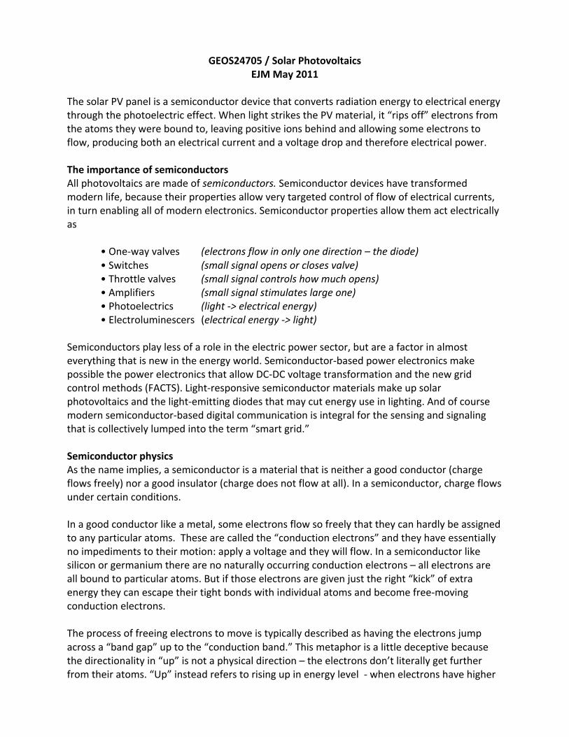
Semiconductors play less of a role in the electric power sector, but are a factor in almost everything that is new in the energy world. Semiconductor-‐based power electronics make possible the power electronics that allow DC-‐DC voltage transformation and the new grid control methods (FACTS). Light-‐responsive semiconductor materials make up solar photovoltaics and the light-‐emitting diodes that may cut energy use in lighting. And of course modern semiconductor-‐based digital communication is integral for the sensing and signaling that is collectively lumped into the term “smart grid.” Semiconductor physics As the name implies, a semiconductor is a material that is neither a good conductor (charge flows freely) nor a good insulator (charge does not flow at all). In a semiconductor, charge flows under certain conditions. In a good conductor like a metal, some electrons flow so freely that they can hardly be assigned to any particular atoms. These are called the “conduction electrons” and they have essentially no impediments to their motion: apply a voltage and they will flow. In a semiconductor like silicon or germanium there are no naturally occurring conduction electrons – all electrons are all bound to particular atoms. But if those electrons are given just the right “kick” of extra energy they can escape their tight bonds with individual atoms and become free-‐moving conduction electrons. The process of freeing electrons to move is typically described as having the electrons jump across a “band gap” up to the “conduction band.” This metaphor is a little deceptive because the directionality in “up” is not a physical direction – the electrons don’t literally get further from their atoms. “Up” instead refers to rising up in energy level -‐ when electrons have higher
energies they can conduct freely. Still, it can be a useful mental image to think of the semiconductor electrons being kicked up into a region where they can flow freely.
The conduction electrons are not the only factors in making current flow in semiconductors. As soon as electrons are lifted into the conduction band, it also becomes possible for current to flow in the valence band. Once an electron has been ejected from its tight bond with an individual atom, that atom is left with a “hole”, a place where an electron should be, and the atom now carries a local positive charge because of its missing negative electron. While other electrons in the valence band cannot flow freely, they can make small jumps from being bound to one atom to changing allegiance to a neighboring atom, if a suitable bonding site (a “hole”) is there to receive them. If you apply a voltage across a semiconductor, then, and some electrons have been freed to the conduction band, what results is a net current comprised of two components: a flow of negative free electrons and a simultaneous flow of positive “holes” in the opposite direction, as the valence electrons reshuffle themselves. Semiconductor junctions Uniform semiconductor materials alone are not particularly useful. What makes semiconductors so useful is when two materials of slightly different properties are placed adjacent to each other. These semiconductor “junctions” are the basis of modern electronics. The components of a semiconductor junction are not pure materials but are intrinsic semiconductors that have been “doped” with certain impurities that make it easier for particular kinds of charge to flow. In an “n-‐type” (n for “negative) semiconductor, the dopant is an element that “likes” to contribute free electrons but does not like to accept electrons in the spot they are freed from. (For people with chemistry background, n-‐type dopants are pentavalent – they have five electrons in their outermost shell, so that the loss of one would leave a complete 4-‐electron shell). The n-‐type dopant therefore gives a soure of free electrons without corresponding holes. In a “p-‐type” semiconductor (p for “positive”), the dopant is the reverse, an element that “wants” to grab free electrons, and so can be considered to contribute extra holes. (Again for people with chemistry background, p-‐type dopants are trivalent). The simplest semiconductor junction is the union of a p-‐type and an n-‐type semiconduction and is termed (creatively) the “p-‐n junction”. It is this doping that makes semiconductors in general and solar photovoltaics in particular dependant on exotic materials. Typical pentavalent (extra electron) n-‐type dopants include antimony, arsenic, and phosphorus. Typical trivalent (needing just one more electron) p-‐type dopants include boron, aluminum, gallium, and indium. These are marked on the periodic table

below. Note that not only the dopants but also the most common intrinsic semiconductor materials themselves (silicon, germanium) all fall along the border between metals and non-‐metals in that confusing regime where elements have some metal-‐like properties (electrons can flow, but not easily).
(Note: most solar PV to date has been made of doped silicon, but new designs are using more exotic semiconductor material, such as CdS and CdTe). When semiconductors of the two types are mated together, the resulting junction acts somewhat as a one-‐way valve. First, remember that the dopant holes cannot flow across the junction – they are property of the atoms that are structurally bound to the material. The only
p-type dopants n-type dopants intrinsic semiconductors

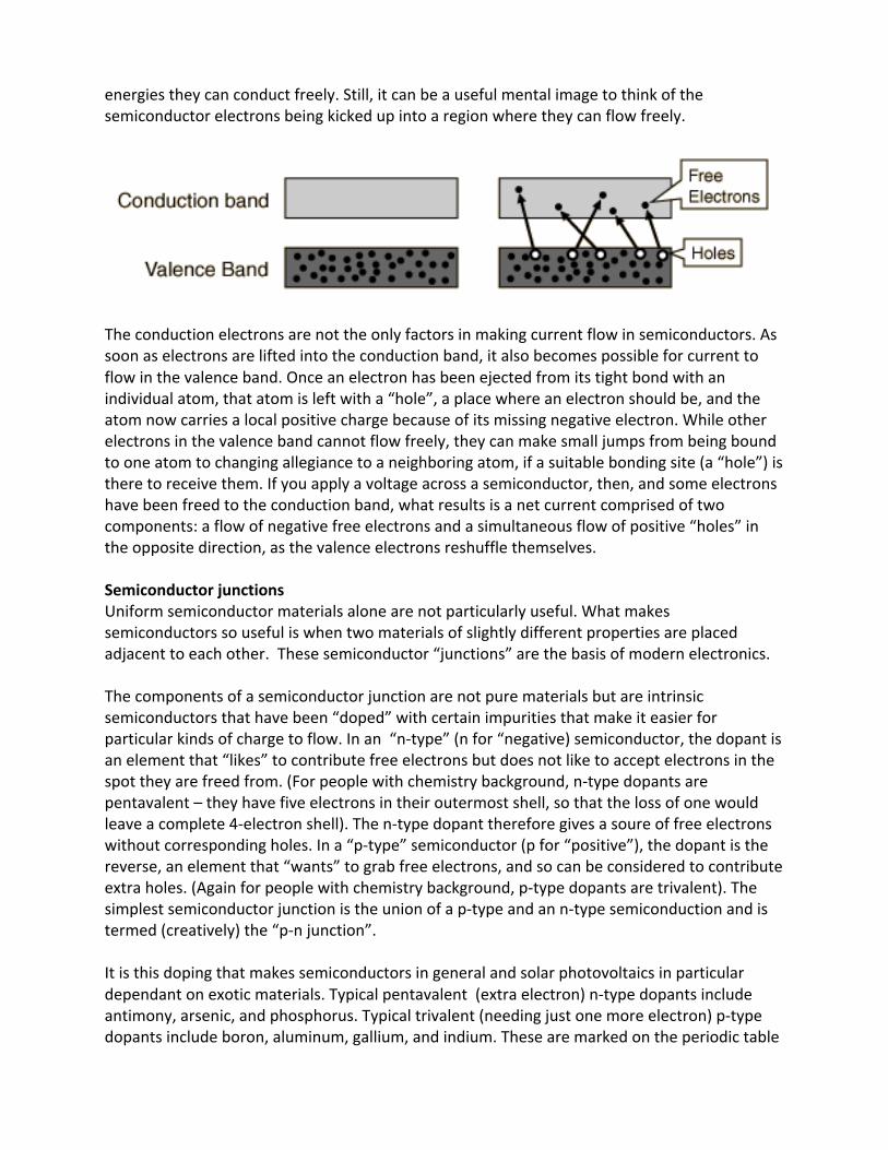
charge that can actually cross the junction is the electrons. And the p side doesn’t have any readily free-‐able electrons to contribute to flow to the n side. Unless you somehow rip electrons away from the p-‐side semiconductor material (usually a destructive process that causes irreversible damage), you can’t move them to the n side. It is easier to push electrons the other way, from n to p, since they are already free in the conduction band. They do need a bit of help, however. To get charge to flow you have to overcome a certain natural resistance to flow that occurs because at the vicinity of the junction, some free electrons do diffuse across and combine with holes on the other side, leaving a slight excess of negative charge on the p side and inhibiting any further flow. In the figure above, that effect is indicated by rise on the p side of the energy levels of electrons -‐ to flow to the p side, electrons would have to be given some energy in order to make it over this energy barrier. That is, you would have to apply an external voltage to allow more charge to flow. For most common semiconductor junctions, that voltage is quite low, ~ 0.6 V. Once that barrier is overcome, though, charge can flow freely: electrons from the n-‐side cross the p-‐n junction and travel through the p-‐side, hopping from hole to hole. The p-‐n junction therefore acts normally as a one-‐way valve: highly resistant to flow in one direction, but if only a small voltage is applied in the other direction, current flows unimpeded. It is this property that makes the junction so incredibly useful. (One note: be careful when drawing intuition from the p-‐n junction figure, because it is representing energy levels of electrons, whereas voltage is defined inversely, in terms of the energies of hypothetical positive charges ... If you remember back to the history of electric motors, this occurred because of early confusion over charges and currents, which ended up with the moving charge, the electron, unfortunately labeled as the negative one. To push electrons uphill to the p side, the normal diode direction, you need to apply your 0.6V push as a positive voltage on the p side). Light-‐emitting diodes and photovoltaics Light-‐emitting diodes (LEDs) and photovoltaics (PVs) are both specialized semiconductor diodes in which electrical current is associated with light, either with losing some electrical energy as radiation (in the LEDs) or with the current and electrical energy being driven by radiation energy (in the PVs). In an LED, electrons that are pushed across the p-‐n junction in the normal diode direction (n-‐>p) release energy as light. In a PV, light absorbed at the p-‐n junction breaks apart some of the electron-‐hole pairs that have combined there, letting electrons flow back in the p-‐>n direction. Think of the LED/PV pair just as you do the motor/generator pair, as the same device that can be run in either direction. Much as a generator is a motor run backwards
~ 0.6 V
breakdown voltage
(mechanical-‐> electrical energy instead of electrical-‐> mechanical), a PV is an LED run backwards (light -‐> electrical energy instead of electrical-‐>light). Note that neither the LED nor the PV is compatible with AC power – a one-‐way device can neither be driven by alternating current nor can produce alternating current. The LED requires a DC power source (or a rectifier) and the solar photovoltaic produces DC power (which must be converted to AC with an inverter if it is to be put on the grid).
A light-‐emitting diode is a specialized variant of the diode whose current flow produces light. As in all diodes, electrons can be pushed by an applied voltage from the n to the p side, where they can flow by hopping from hole to hole. (That movement is also referred to as an effective flow of holes). In an LED, when the flowing electrons first recombine with a p-‐side hole, they lose significant energy and that energy is emitted in the form of radiation. (This is termed “radiative recombination”). The wavelength (color) of the emitted light is a function of the energy change and so of the material properties. The LED therefore allows a direct conversion of electrical energy radiation energy, with color choice provided by careful engineering of materials. Each LED can produce only a single wavelength, but is possible to reproduce the broadband spectrum of the sun that people find pleasant with several different strategies – either combining several LEDs of different wavelengths, or coating the LED with a phosphorescent material that absorbs and then re-‐emits the light at different wavelengths. Most white LEDS sold for consumer use the phosphorescence approach (as you saw in the lighting lab, when the LED produced a broadband output). Expensive theatrical or commercial lighting will use the multi-‐color LED approach, often with LEDs separately controlled for computer-‐controllable output color. Radiative recombination in LEDs is highly energy efficient – a very large fraction of the applied energy comes out as light – making the LED a significantly energy-‐saving alternative to the ~2% efficiency incandescent bulb, in which electrical energy is used to heat a filament that then glows and emits light. The newest LEDs should also beat fluorescents, but the phosphorescent coating does degrade their efficiency somewhat – it’s another energy conversion step (radiation -‐> chemical -‐> radiation).
In the LED, when you apply voltage across junction and push electrons through from n to p, energy from that push is released as light. Electrons continue through the p side as normal for diodes.
In the photovoltaic cell, light absorbed near the junction frees electrons and lets them flow to the n side. (Meanwhile electrons from the p-side atoms move into the now vacant holes at the junction).
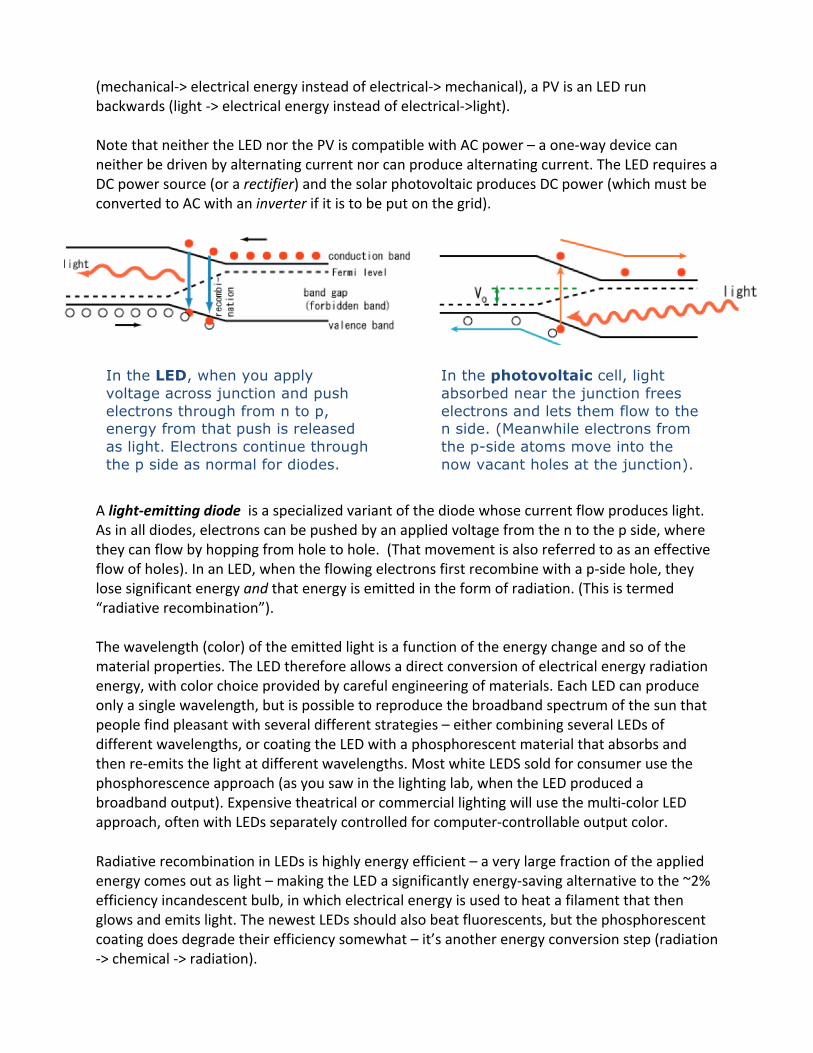
A photovoltaic, as stated above, is essentially an LED run backwards. While in an LED an external energy source pushes electrons “uphill” from n to p, emitting light in the process, in a PV, light incident on the semiconductor junction breaks apart existing electron-‐hole pairs in the junction region, lifting the electrons to the conduction band and letting them flow “downhill” to the n side. A PV kept in the dark acts just like a normal diode. if it is illuminated, though, a current spontaneously flows in the opposite direction from the normal diode current. Think of an illuminated photovoltaic as one where you’ve managed cleverly to use light to push current in the “wrong” direction without the destructive means you’d usually have to resort to (imposing a voltage so high you rip off electrons from the p side but damage the material in the process). Instead the light non-‐destructively provides those free electrons for you. The figure to the right show the I-‐V diagram for a normal diode (in red), where no current can flow in the reverse direction, but current can flow freely if you overcome the diode voltage drop of ~0.6 V. In an iiluminated photovoltaic, current flows spontaneously in the anti-‐diode direction.
(Image: Alan Doolittle, Georgia Tech) PV behavior The short summary of how to think about photovoltaic behavior is that everything is backwards from the industrial AC generators we discussed earlier. The industrial generator “wants” to maintain a constant voltage (or at least, its operator tries to run his turbine so as to keep voltage constant). Because of that, the current put out by the generator varies with the resistance of the load, with lower resistances drawing more current and therefore more power. A photovoltaic, by contrast, “wants” to maintain a constant current. Because of that, the voltage across the photovoltaic varies with the resistance of the load, with higher resistances producing higher voltages and therefore drawing more power. PV behavior: a solar photovoltaic acts like a current source under low load The key to understanding photovoltaic behavior is to realize that for most normal PV operation, the current that is produced is proportional to light level: every electron that is released at the diode junction by the incident light keeps flowing. This means though that current is constant regardless of what the PV is hooked up to – a very strange concept, that current should be independent of load! That’s not at all what we found for ordinary industrial generators that convert mechanical motion to electrical energy. (Those were operated at constant voltage, and the current depended on what the load was). In a photovoltaic in normal operation, the current
short circuit current (voltage is zero)
open circuit voltage (current is zero)

is constant, since it is determined by the light, and the voltage then varies according to the load. It may help to think about this behavior starting with the endmember case, thinking of a photovoltaic exposed to a constant light level but with no resistive load at all. If you wire the one side of a PV to the other with a simple wire (resistance effectively zero) and expose it to light, every electron released by the incident light will happily flow, while doing essentially no work. Unlike the generators you’ve seen so far, you can short-‐circuit a photovoltaic with no ill effects – you won’t blow out the PV. Since P=IV and I is fixed but no work is done (P=0), the voltage across the “short circuit” photovoltaic must be zero. If you add a resistance (like a lightbulb) to the circuit, the photovoltaic will still want to push a constant current across it. Since by Ohm’s law V=IR, and the photovoltaic is keeping I constant, the voltage across the photovoltaic is directly proportional to R. That is, the PV panel adjusts its voltage to match whatever resistance is attached to keep a constant current flowing. How much power is delivered to the load? Since P=IV, and I is fixed in this regime, the power transferred to the load is a function of the load itself (P=I2R). Unlike what you’ve seen before, the larger the resistance, the larger the output power. In the low load range, increasing resistance increases the power output. PV behavior: a solar photovoltaic acts like a voltage source under high load. Of course, a PV panel can’t put out constant current regardless of how big a resistance you attach to it, if power delivered goes up with resistance. The sun only has so much power, and as you increased the “demand” for power, eventually the PV would no longer be able to keep up. That is, it could not physically continue to put out constant current anymore – something must give. In fact, in the high-‐load range – when the photovoltaic is hooked up to too large a resistance -‐ the PV panel acts much like the electrical generators we discussed earlier. That is, it acts like a constant voltage source, wanting to keep a constant voltage difference across its terminals, and reducing current accordingly. Since V = IR by Ohm’s law, if V is constant we get that current is proportional to 1/R. Now as we increase the resistance past the point where the photovoltaic can’t keep up, less current flows. Since power P=IV, if V ~ constant then P~ V2/R, and the bigger the resistor the lower the power. In the high load range, adding resistance reduces the power output. If you combine those behaviors you’ll see that if you gradually increase the resistance of the load on a photovoltaic, for awhile current is constant and the voltage across the PV panels gradually increases, which in turn means that power delivered increases. That works until you hit the peak power that the photovolataic can put out (which happens at a voltage close to the diode voltage drop of ~0.6 V). From that point on, the PV is at its maximum voltage – increased any more and the current would start flowing backwards. From here, continuing to increase the resistance of the load results in a very swift crash in current. When resistance is infinitely high no current can flow and the photovoltaic is effectively “open circuit” . At this point all the released electrons have nowhere to go – they just stack up until the voltage induced by that charge exactly cancels the 0.6 V diode drop and no current flows.

The practical consequence of this behavior is that you can’t think of the power produced by the photovoltaic separately from the load it is connected to, and you had better match your load very closely to the panel if you want optimal power generation.
This figure shows the same I-V diagram as the previous figure, only now flipped over. (We just redefined the direction of the current to be positive – that’s normal for thinking about photovoltaics). Since P = I*V, the maximum power point is that point where the arrow from the origin to the I-V curve is longest. Photovoltaic specifications: The specifications given on a photovoltaic are its rated (i.e. maximum) power, its “open-‐circuit” (no current) voltage, and its “short circuit” (no voltage) current. If the I-‐V curve were a perfect rectangle, the rated power would be the short-‐circuit I x the open-‐circuit V, but in actuality is a bit less. Panel numbers are given calibrated to an illumination level of 1000 W/m2. Varying the light level. Increasing the illumination on a photovoltaic doesn’t change the I*V behavior pattern. More light does free more electrons, though, so the photovoltaic puts out more current in its constant-‐current mode, and therefore more total power. The short-‐circuit current is approximately linear with illumination – twice the light = twice the current, which yields four times the power since P = I2R. The voltage at which current must drop necessarily remains the same at the intrinsic diode drop.
P = I*V

Photovoltaic materials and construction Most commercial solar panels are made of polycrystalline silicon. As of 2008, only twelve factories in the world produced this material, and more than half the poly silicon of sufficiently high grade was going to the production of solar cells. All the panels that we we have to play with are polycrystalline silicon, and you can see the grain boundaries between distinct silicon crystals. Commercial photovoltaics are increasingly made using semiconductor materials deposited in thin films rather than grown as crystals, of which the most common are cadmium telluride / cadmium sulfide and amorphous silicon. Thin-‐film cells are lower in efficiency, but the hope is that the manufacturing can become cheaper than for crystalline silicon, making them the more economical choice. Thin films are also less subject to breakage. PV panel arrangements Individual solar photovoltaic cells are quite small (1-‐10 cm on a side). The larger solar panels that you see as self-‐contained units are actually many individual PV cells wired together. Since (as mentioned above) each cell can only produce a very small voltage (~0.6 V), it is normal to wire many cells in series – one after another like beads on a string – to form a module so that the overall voltage of the panel is the sum of the voltage drops across all the individual cells. Individual modules are themselves wired together in a single panel, either in series or in parallel. Finally, because individual solar panels produce relatively little energy (even at peak insolation of ~ 1000 W/m2 a 15% efficiency panel of 1m2 will produce only 150 W, enough for perhaps two lightbulbs), any practical solar PV system consists of many panels. The panels are not separately wired to the inverter but again are connected, again often in series.
Partial shading One very large drawback of the series wiring of PV modules, panels, and systems is that the entire panel/module/system is then electrically connected, and problems in any part affect the overall power level. Series-‐wired panels show a strong and very negative “partial shading” response, drops in power when the panel receives uneven sunlight. The partial shading response is strongly nonlinear: if you shade a tenth of your panel, your power may go down by 50%. This make panel installation problematic in locations where there are any potential shade obstacles (shadows from trees or buildings, falling leaves, passing clouds). PV panels really work
Single photovoltaic cells (1) connected in series form a photovoltaic module (2). Several modules assembled together create a photovoltaic panel (3). Image from scienza giovane (Univ. Bologna).

best in in the desert, in bright cloudless places with uniform illumination, little water vapor to make clouds and no trees to drop leaves or make shadows. The key issue for why partial shading affects a solar cell so dramatically is that series wiring means that if any current is to flow, it has to flow through them all. It’s obvious that localized damage to one cell could have big consequences. If you broke one cell altogether, for example, so that nothing could flow through it, you'd have a total panel failure even though the damage was in one small area, because you'd have prevented all current flow. If you completely shade one solar cell, you remove its ability to pass current, almost as though you had damaged it. Now the cell is a diode, and you are trying to push current the wrong way through a diode. The cell becomes a bottleneck. Partial shading or even just non-‐uniform illumination thus produces a conflict between the current that different cells want to pass, a disagreement that has to be remedied (since the same current does have to pass through all the cells). In this adjustment, the whole panel adjusts to a non-‐optimal operation to push any current at all through it. From the I-‐V curve for a photovoltaic you can see power drops dramatically if the photovoltaic is overloaded. For a grid-‐connected panel, the inverter (DC-‐> AC converter) to which the panel is connected essentially puts a fixed load on the system, optimized for the illumination that you’d expect to have. The response to overload is very sharp though: power falls steeply if the load is just a bit too high. If some of the cells are knocked out, you basically put the whole panel in this overload state and see a very sharp reduction in total power. Another nasty side effect of partial shading is that pushing current through a solar cell that's not illuminated takes power, rather than consuming power. This is a relatively minor effect on total panel performance but does mean that the individual shaded solar cell will heat up, which can in turn lead to actual permanent failure. Shade one cell and its neighbors can fry it, ruining the entire panel forever. This is yet another reason why residential solar or solar in intermittently cloudy place is problematic. In the past, these kind of partial shading problems often arose for entire solar installations whose separate panels were wired in series. Partial shade on one panel would mess up that panel, and the messed-‐up panel would then degrade the whole solar PV installation. Modern installations now often have bypass systems included to let current keep flowing in case one of the panels malfunctions. Smarter inverters also adjust the load as if panel performance is dropping to at least minimize problems and keep the system near its optimal performance. Performance in cloudy conditions Solar panel output power drop sharply on a cloudy day, even when there is enough light to see well by, for much the same reason as the drop for partial shading. Again, if your system no longer has enough “push” from the sun but the load on it is fixed, it falls into the overload state and current and power drops sharply. A bit of drop in light level can compromise panel output severely. This effect can be more severe than your eye would expect, because your eye adjusts so well to changing light levels that you often don’t notice how much light may be changing. Illumination
on a day of thick clouds may be 10 x less than on a clear sunny day. (And light levels indoors are typically also 10 x less than those outdoors). You wouldn’t expect the solar panel to produce power in response to indoor lighting. Nor can it produce power on deeply cloudy days. The eye is a poor guide to incident power has evolved to allow you to see in as wide a range of light as possible: it is basically logarithmically sensitive, and you have a variable aperture in the front (your pupil expands and contracts) which further increases your dynamic range. The solution for the cloudy-‐day problem is to have a smarter inverter than can adjust the load as needed, so that it can keep the system from going into its "not enough push" shutdown mode. With a smart inverter, you get less power out than in the optimal illumination case, but at least you'd get some power. In a real solar array, electronics in the inverter the connects a solar array to the grid can be designed to do just that, to compensate for changing illumination by effectively asking for less power when less power is available. You'll still get losses on a cloudy day, but you minimize them by not asking the system to give you something it just can't do. Lab activities In this lab you can play with some solar panels and explore their characteristics. Below are some suggestions for activities that illustrate the performance of solar panels.
• Use a panel to turn an electric motor or motors. Observe how the motor speed varies with illumination.
• Verify that panels behave as specified – measure the open-‐circuit voltage and short-‐circuit current and compare to the specs on the back of the panel.
• Directly observe the panel’s changing current output with illumination. The easiest way to do this is to short-‐circuit the panel through a current meter (a multimeter in current mode) so that you’re measuring the short-‐circuit current, and then change the panel illumination either by tilting it toward and away from the sun, or using a filter to cut down the sunlight, or (with some care) even concentrating light on the panel with a lens. (The last is hard to do because it takes some finesse to get even illumination across the panel). Measure solar radiation with the solar power meter and verify that the current response is linear with power from the sun.
• Test and observe the non-‐linear power dropoff that results from partial shading. For this you have to have some load on the panel – you need to hook it up to a resistor or a motor. You can measure both current and voltage to get a direct measure of power, or you can get a qualitative sense by watching a motor slow down noticeably when the panel is partially shaded.
• Test the efficiency of the panel by comparing the solar insolation (in W/m2, from which you know the total W striking the panel) to its output power when driving a load. You should get an efficiency somewhere around 15% for a optimized load.
• Map out the I-‐V curve of the panel – measure I and V simultaneously for different loads. • Using colored filters, test the response of the PV panel power to different frequencies
(colors) of light -‐ is it equally sensitive to the red, green, and blue parts of the spectrum?

• Verify viscerally the sun’s power by using a Fresnel lens to concentrate power on a thermometer and heat it, or (even more viscerally) light something on fire with it. The Fresnel lenses inside old projection TVs, if taken out and put in the sun, can generate temperatures high enough to melt a penny. (You know the mirrors in a solar PV installation can produce temperatures of over 500 C, as hot as the metal of the boiler system will stand; the melting point of copper is 1000 C).
E. Moyer 2011