generation and transfer of single photons on a photonic...
TRANSCRIPT

Generation and transfer of single photons on a
photonic crystal chip
Dirk Englund, Andrei Faraon, Bingyang Zhang, Yoshihisa Yamamoto,and Jelena Vuckovic
Ginzton Laboratory, Stanford University, Stanford CA 94305
Abstract: We present a basic building block of a quantum networkconsisting of a quantum dot coupled to a source cavity, which in turn iscoupled to a target cavity via a waveguide. The single photon emission fromthe high-Q/V source cavity is characterized by twelve-fold spontaneousemission (SE) rate enhancement, SE coupling efficiencyβ ∼ 0.98 into thesource cavity mode, and mean wavepacket indistinguishability of∼67%.Single photons are efficiently transferred into the target cavity via thewaveguide, with a target/source field intensity ratio of 0.12± 0.01. Thissystem shows great promise as a building block of future on-chip quantuminformation processing systems.
© 2007 Optical Society of America
OCIS codes: (130) Integrated optics; (130.2790) Guided waves; (130) Integrated optics;(130.3120) Integrated optics devices; (270) Quantum Optics; (270.5580) Quantum electrody-namics; (000.1600) Classical and quantum physics; (140.3410) Laser resonators; (140.5960)Semiconductor lasers; (230) Optical devices; (230.5750) Resonators; (230.6080) Sources;(250) Optoelectronics; (250.5300) Photonic integrated circuits
References and links1. D. Bouwmeester, J. Pan, K. Mattle, M. Eibl, H. Weinfurter, and A. Zeilinger, “Experimental quantum teleporta-
tion,” Nature390, 575–9 (1997).2. E. Knill, R. Laflamme, and G. J. Milburn, “A scheme for efficient quantum computation with linear optics,”
Nature409, 4652 (2001).3. M. A. Nielsen and I. L. Chuang,Quantum Computation and Quantum Information(Cambridge Univ. Press,
Cambridge, 2000).4. P. Grangier, B. Sanders, and J. Vuckovic, “Single photons on demand,” New Journal of Physics6 (2004).5. P. Michler, ed.,Single quantum dots: Fundamentals, Applications, and New Concepts(Topics in Applied Physics,
Springer-Verlag, 2003).6. C. Santori, D. Fattal, J. Vuckovic, G. S. Solomon, and Y. Yamamoto, “Indistinguishable photons from a single-
photon device,” Nature419(6907), 594–7 (2002).7. J. I. Cirac, P. Zoller, H. J. Kimble, and H. Mabuchi, “Quantum State Transfer and Entanglement Distribution
among Distant Nodes in a Quantum Network,” Phys. Rev. Lett.78(16), 3221–24 (1997).8. A. Imamoglu, D. D. Awschalom, G. Burkard, D. P. DiVincenzo, D. Loss, M. Sherwin, and A. Small, “Quantum
Information Processing Using Quantum Dot Spins and Cavity QED,” Phys. Rev. Lett.83(20), 4204–4207 (1999).9. C. Monroe, D. M. Meekhof, B. E. King, W. M. Itano, and D. J. Wineland, “Demonstration of a Fundamental
Quantum Logic Gate,” Phys. Rev. Lett.75(25), 4714–4717 (1995).10. J. Chiaverini, D. Leibfried, T. Schaetz, M. D. Barrett, R. B. Blakestad, J. Britton, W. M. Itano, J. D. Jost, E. Knill,
C. Langer, R. Ozeri, and D. J. Wineland, “Realization of quantum error correction,” Nature432, 602–5 (2005).11. D. A. Fattal and Y. Yamamoto, “Single photons for quantum information processing,” Ph.D. thesis, Stanford
University (2005).12. W. Yao, R. B. Liu, and L. J. Sham, “Theory of Control of the Spin-Photon Interface for Quantum Networks,”
Phys. Rev. Lett.95, 030,504 (2005).13. B. B. Blinov, D. L. Moehring, L.-M. Duan, and C. Monroe, “Observation of entanglement between a single
trapped atom and a single photon,” Nature428, 153–7 (2004).14. Y. Akahane, T. Asano, B.-S. Song, and S. Noda, “High-Q photonic nanocavity in a two-dimensional photonic
crystal,” Nature425, 944–947 (2003).
#80664 - $15.00 USD Received 5 Mar 2007; revised 10 Apr 2007; accepted 11 Apr 2007; published 23 Apr 2007
(C) 2007 OSA 30 Apr 2007 / Vol. 15, No. 9 / OPTICS EXPRESS 5550

15. D. Englund and J. Vuckovic, “A direct analysis of photonic nanostructures,” Opt. Express14(8), 3472–83 (2006).16. E. Waks and J. Vuckovic, “Coupled mode theory for photonic crystal cavity-waveguide interaction,” Opt. Express
13, 5064–73 (2005).17. D. Englund, D. Fattal, E. Waks, G. Solomon, B. Zhang, T. Nakaoka, Y. Arakawa, Y. Yamamoto, and J. Vuckovic,
“Controlling the Spontaneous Emission Rate of Single Quantum Dots in a Two-Dimensional Photonic Crystal,”Phys. Rev. Lett.95, 013,904 (2005).
18. A. Faraon, E. Waks, D. Englund, I. Fushman, and J. Vukovic, “Efficient photonic crystal cavity-waveguide cou-plers,” Appl. Phys. Lett.90, 073,102 (2007).
19. A. Kiraz, M. Atature, and I. Imamoglu, “Quantum-dot single-photon sources: Prospects for applicationsquantum-information processing,” Phys. Rev. A69, p.032,305–1–032,305–10 (2004).
20. S. Laurent, S. Varoutsis, L. Le Gratiet, A. Lemaıtre, I. Sagnes, F. Raineri, A. Levenson, I. Robert-Philip, andI. Abram, “Indistinguishable single photons from a single-quantum dot in a two-dimensional photonic crystalcavity,” Appl. Phys. Lett.87, 3107 (2005).
21. J. Vuckovic, D. Englund, D. Fattal, E. Waks, and Y. Yamamoto, “Generation and manipulation of nonclassicallight using photonic crystals,” Physica E Low-Dimensional Systems and Nanostructures32, 466–470 (2006).
22. H. N. et al., “Ultra-fast photonic crystal/quantum dot all-optical switch for future photonic networks,” Opt. Ex-press12, 6606–6614 (2004).
1. Introduction
Recent years have witnessed dramatic practical and theoretical advancements towards creatingthe basic components of quantum information processing (QIP) devices. One essential elementis a source of single indistinguishable photons, which is required in quantum teleportation[1],linear-optics quantum computation[2], and several schemes for quantum cryptography [3].Sources have been demonstrated from a variety of systems[4] including semiconductor quan-tum dots (QDs)[5], whose efficiency and indistinguishability can be dramatically improved byplacing them inside a microcavity[6]. A second major component is a quantum channel for ef-ficiently transferring information between spatially separated nodes of a quantum network[7].This network would combine the ease of storing and manipulating quantum information inQDs[8], atoms or ions[9, 10], with the advantages of transferring information between nodesvia photons, using coherent interfaces[11, 12, 13]. Here we demonstrate a basic building blockof such a quantum network by the generation and transfer of single photons on a photoniccrystal (PC) chip. A cavity-coupled QD single photon source is connected through a 25µmchannel to an otherwise identical target cavity so that different cavities may be interrogatedand manipulated independently (Fig. 2). This system provides a source of single photons witha high degree of indistinguishability (mean wavepacket overlap of∼ 67%), 12-fold SE rateenhancement, SE coupling factorβ ∼ 0.98 into the cavity mode, and high-efficiency couplinginto a waveguide. These photons are transferred into the target cavity with a target/source fieldintensity ratio of 0.12±0.01 (up to 0.49 observed in structures without coupled QDs), showingthe system’s potential as a fundamental component of a scalable quantum network for buildingon-chip quantum information processing devices.
2. Photonic network
The structure consists of two linear 3-hole defect cavities[14], butt-coupled and connected via a25 µm-long closed portion of a waveguide (Fig. 2(a)). It was designed by component-wise Fi-nite Difference Time Domain (FDTD) simulations in three dimensions. The waveguide designshown here supports four bands; we picked bandBoe to transfer light between the end-cavities(Fig. 2(b)). This band offers a wide, relatively flat spectral region of guided modes for couplingand can furthermore be confined in the high-Q end-cavities. Thanks to their near-minimummode volumeVmode≡ (
∫V ε(~r)|~E(~r)|2d3~r)/max(ε(~r)|~E(~r)|2)≈ 0.74(λ/n)3, these end-cavities
allow a large SE rate enhancement∝ Q/Vmode.The cavity and waveguide field decay rates can be expressed as a sum of vertical, in-plane,
and material loss, respectively:κ = κ⊥ + κ‖,wg+ γ. Removed from the waveguide, the ‘bare’
#80664 - $15.00 USD Received 5 Mar 2007; revised 10 Apr 2007; accepted 11 Apr 2007; published 23 Apr 2007
(C) 2007 OSA 30 Apr 2007 / Vol. 15, No. 9 / OPTICS EXPRESS 5551

outer cavities radiate predominantly in the vertical direction at rateκ⊥, as in-plane losses canbe suppressed with enough PC confinement layers. Introducing an open waveguide coupled tothe cavity creates additional lossκ‖,wg.
In a waveguide of finite extent, the continuum of modes in the waveguide band breaks upinto discrete resonances. For photon transfer, one of these must be coupled to the outer cavities.Assuming the two cavities are spectrally matched and detuned from the waveguide resonanceby ∆, and that material lossesγ are negligible [15], the field amplitudes in the source and targetcavities (S,T) and waveguide (W) evolve according to:
cs(t) = −iκ‖cw(t)−κ⊥cs(t)+ p(t)ct(t) = −iκ‖cw(t)−κ⊥ct(t) (1)
cw(t) = −iκ‖cs(t)− iκ‖ct(t)− (κW + i∆)cw(t)
Here we assume equal coupling rates for the outer cavities, based on their near-identical SEMimages andQ values, which fall within a linewidth of each other in most structures. The con-stantκW denotes the waveguide loss rate (other than loss into the end-cavities), andp(t) rep-resents a dipole driving the source cavity. It will suffice to analyze this system in steady-statesince excitation of the modes, on the order of the exciton lifetimeτ ∼ 100 ps, occurs slowlycompared to the relaxation time of the photonic network, of orderτ = ω/Q∼ 1 ps for the cav-ity and waveguide resonances involved. Then the amplitude ratio between the S and T fields iseasily solved ascs/ct = 1+κ⊥(κW + i∆)/κ2
‖ .
g
ego
κ
κ
κW
Γ
Cavity S Cavity TWaveguide
κ
κ
Fig. 1. Basic network consisting of two cavities and one cavity-coupled QD. The QD is coupled toa cavity (rateg0) and decays with SE rateΓ. The cavity, in turn, is coupled to a waveguide and leakymodes at field coupling ratesκ‖ andκ⊥, respectively. The waveguide field decay rate isκW.
In the present application, we used FDTD simulations to optimize a design with high transferrate, while retaining high field confinement in the source cavity for enhancing the SE rate ofcoupled QDs. Due to computational constraints, optimization was performed for the case of acavity connected to an open, 9-period waveguide terminated with absorbing boundary condi-tions (Fig. 2). The cavity resonances were targeted to a linear region of the waveguide dispersionwith group velocityVg = 0.3c/n,n= 3.5, slightly above the lower waveguide cut-off frequency(see Fig.2). In this way, we limited pulse dispersion and made the design more tolerant to fab-rication inaccuracies. The closed-waveguide coupling constantκ‖ was then calculated from theopen-waveguide valueκ‖,wg by accounting for the different densities of states in the two cases1,giving κ‖/κ⊥ ≈ 15.
The structures were fabricated on a 160 nm-thick GaAs membrane, grown by molecular-beam epitaxy with a central layer of self-assembled InAs QDs whose photoluminesce (PL)peaks at 932 nm with an inhomogeneous linewidth of∼ 60 nm and a density of∼ 200QDs/µm2. The structures were fabricated by electron beam lithography and reactive ionetching, followed by a wet chemical etch to remove a sacrificial layer underneath the PCmembrane[17]. Among the 30 fabricated structures, we experimentally found that fabrication
#80664 - $15.00 USD Received 5 Mar 2007; revised 10 Apr 2007; accepted 11 Apr 2007; published 23 Apr 2007
(C) 2007 OSA 30 Apr 2007 / Vol. 15, No. 9 / OPTICS EXPRESS 5552

Cavity T
(a)
Cavity S
(b) Log|E|
2r
a
w
2r0
Hz0.2
0.3 B eo B ee B
kx a/π0 0.2 0.4 0.6 0.8 1
light lineBoe
a/λ
Cavities S,T0.2 0.4 0.6 0.8 1
2r02r1
2 µm
Fig. 2. Coupled cavities system. (a) The identical source (S) and target (T) cavities are connectedvia the 25-µm. Design parameters: PC,a = 256 nm,r0 = 0.3a. Outer cavities,r1 = 0.25a, r0 = 0.3a.Waveguide,rw = 0.25a for the bounding rows of holes.Inset: Electric field pattern. (b) Waveguidedispersion diagram showing bandBoe used for photon transfer. The cavity resonance intersects theband’s linear dispersion region just belowkx = π/a (field pattern in inset).
inaccuracies reduced totalQ values to 1560±550, neglecting one outlier withQs = 5100,Qt =4900 for the source and target cavities.
We now focus on a particular system that showed high coupling among cavities, while alsoexhibiting large QD coupling in the source cavity. Measurements were done with the sampleat 5K in a continuous-flow cryostat and probed with a confocal microscope setup as shownin Fig. 3. A movable aperture in the microscope image plane, together with a stir-able pumpbeam, allow independent adjustment of the pump and observation regions. The structures werecharacterized by measuring the combinations of pump/probe regions (waveguide ‘WG’, sourcecavity ‘S’, or target cavity ‘T’). Here the broad-band PL of high-intensity, above-band pumpedQDs was used as an internal illumination source. Fig. 4(a) shows good spectral match be-tween direct measurements of the source/target cavities (plots ‘SS’ and ‘TT’), together withthe coupled emission (plots ‘ST’ and ‘TS’). Comparison the emission intensities from S andT cavities gives the transfer efficiency|ct/cs|2 = 0.12±0.01. This transfer occurs through oneof the resonances of the terminated waveguide, which we can illuminate by pumping near thecenter. PL that is resonant inside the waveguide, but off-resonant from the cavities, is scat-tered primarily at the waveguide/cavity interfaces. On the other hand, PL that is resonant withthe cavities is dropped into them and can be spatially separated with the pinhole. This drop-filtering is shown in 4(b), where the bottom plot (‘WG-all’) shows all modes resonant in thecoupled system, while the top two plots ‘WG-WG’ and ‘WG-T’ show collection from only thewaveguide terminus and the cavity, respectively. Fitting the measurements of panels (a,b) tothe frequency-domain model in Eq.1 gives the coupling coefficientsκ⊥ = 455 GHz,κW = 322GHz, κ‖ = 283 GHz. The waveguide-coupling ratioκ‖/κ⊥ is about 24× lower than expectedfrom the simulated design. This drop is caused by fabrication errors, which primarily affect
#80664 - $15.00 USD Received 5 Mar 2007; revised 10 Apr 2007; accepted 11 Apr 2007; published 23 Apr 2007
(C) 2007 OSA 30 Apr 2007 / Vol. 15, No. 9 / OPTICS EXPRESS 5553
laser polarizationanalyzer
HBT
t1
t2time-interval analyzer
2 ns
2 ns
HOM
L
S
streak camera
spectrometer
cav.T
cav.S
pump
cryostatcryostatcryostatcryostat
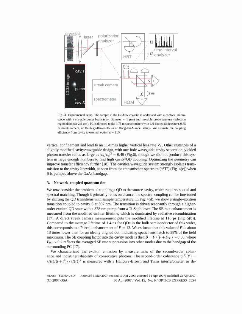
Fig. 3.Experimental setup. The sample in the He-flow cryostat is addressed with a confocal micro-scope with a stir-able pump beam (spot diameter∼ 1 µm) and movable probe aperture (selectionregion diameter 2.9µm). PL is directed to the 0.75 m spectrometer (with LN-cooled Si detector), 0.75m streak camera, or Hanbury-Brown-Twiss or Hong-Ou-Mandel setups. We estimate the couplingefficiency from cavity to external optics at∼ 11%.
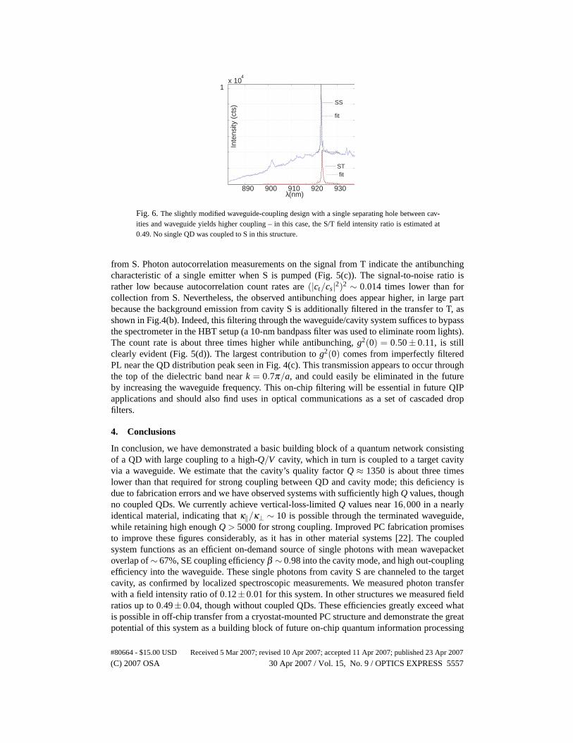
vertical confinement and lead to an 11-times higher vertical loss rateκ⊥. Other instances of aslightly modified cavity/waveguide design, with one-hole waveguide-cavity separation, yieldedphoton transfer ratios as large as|ct/cs|2 = 0.49 (Fig.6), though we did not produce this sys-tem in large enough numbers to find high cavity/QD coupling. Optimizing the geometry canimprove transfer efficiency further [18]. The cavities/waveguide system strongly isolates trans-mission to the cavity linewidth, as seen from the transmission spectrum (‘ST’) (Fig. 4(c)) whenS is pumped above the GaAs bandgap.
3. Network-coupled quantum dot
We now consider the problem of coupling a QD to the source cavity, which requires spatial andspectral matching. Though it primarily relies on chance, the spectral coupling can be fine-tunedby shifting the QD transitions with sample temperature. In Fig. 4(d), we show a single-excitiontransition coupled to cavity S at 897 nm. The transition is driven resonantly through a higher-order excited QD state with a 878 nm pump from a Ti-Saph laser. The SE rate enhancement ismeasured from the modified emitter lifetime, which is dominated by radiative recombination[17]. A direct streak camera measurement puts the modified lifetime at 116 ps (Fig. 5(b)).Compared to the average lifetime of 1.4 ns for QDs in the bulk semiconductor of this wafer,this corresponds to a Purcell enhancement ofF = 12. We estimate that this value ofF is about13 times lower than for an ideally aligned dot, indicating spatial mismatch to 28% of the fieldmaximum. The SE coupling factor into the cavity mode is thenβ = F/(F +FPC)∼ 0.98, whereFPC∼ 0.2 reflects the averaged SE rate suppression into other modes due to the bandgap of thesurrounding PC [17].
We characterized the exciton emission by measurements of the second-order coher-ence and indistinguishability of consecutive photons. The second-order coherenceg(2)(t ′) =〈I(t)I(t + t ′)〉/〈I(t)〉2 is measured with a Hanbury-Brown and Twiss interferometer, as de-
#80664 - $15.00 USD Received 5 Mar 2007; revised 10 Apr 2007; accepted 11 Apr 2007; published 23 Apr 2007
(C) 2007 OSA 30 Apr 2007 / Vol. 15, No. 9 / OPTICS EXPRESS 5554

885 890 895 900 905
SS
TT
ST
TS
inte
nsity
(a.u
.)
(a)
λ(nm)885 890 895 900 905
WG-all
WG-T
λ(nm)
(b)
WG-WG800 900 1000 11000
0
1
896 898 900 9020
0.2
0.4
0.6
0.8
1
ST, 0SS, 0SS, 90TT, 0
(c)
(d)
λ(nm)
λ(nm)
SS
ST
0
1
1
0.1
0.1
∆λ=0.69 nm
∆λ=0.68 nm
∆λ=0
.48
nm
O
O
O
O
0.05
0.1
0.5
Fig. 4.Cavity-cavity coupling via a waveguide. (a) Pumping and observation from source (‘S’) andtarget (‘T’) cavities. (b) Cavity-coupling via a waveguide resonance. The waveguide is pumped andemission collected from the full structure (‘WG-all’) or spatially filtered from the waveguide (‘WG-WG’) or cavity T (‘WG-T’). (c) Broad emission in cavity S (plot ‘SS’) is filtered into the target cavity(plot ‘ST’). (d) When the QD exciton at 897.3 nm in cavity S is pumped (resonantly at 878 nm,460 µW, 1µm focal spot), the emission is observed from S (‘SS’) and T (‘ST’). The cross-polarizedspectrum from S shows nearly complete quenching of QD emission (‘SS, 90◦’). The line at 897.3 nmis only observed when S is pumped.
scribed earlier [17]. When the QD in cavity S is pumped resonantly, then photons observed fromS shows clear antibunching (Fig. 5(a)), withg2(0) = 0.35±0.01. This value exceeds measure-ments for cavity-detuned QDs, where typicallyg(2)(0) < 0.05, similar to previous reports[6].The main contributor to the largerg(2)(0) for the coupled QD is enhanced background emis-sion from nearby transitions and the wetting layer emission tail, which decays at∼ 100 ps timescales (see Fig. 5(b)) and is not completely filtered by our grating setup. The background emis-sion is rather large in this study because of the high QD density of the sample (e.g., four timeslarger than that in the experiment bySantori et al.[6]).
Because of the shortened lifetime of the cavity-coupled QD exciton, the coherence timeof emitted photons becomes dominated by radiative effects and results in high photonindistinguishability[19]. We measured the indistinguishability using the Hong-Ou-Mandel(HOM) type setup sketched in Fig. 3, similar to a recent experiment[20]. The QD is excitedtwice every 13 ns, with a 2.3 ns separation. The emitted photons are directed through a Michel-son interferometer with a 2.3 ns time difference. The two outputs are collected with singlephoton counters to obtain the photon correlation histogram shown in the inset of Fig. 5(b). Thefive peaks around delayτ = 0 correspond to the different possible coincidences on the beam-splitter of the leading and trailing photons after passing through the long or short armsL or Sof the interferometer. If the two photons collide and are identical, then the bosonic symmetryof the state predicts that they must exit in the same port. This photon bunching manifests itselfasanti-bunching in a correlation measurement on the two ports. This signature of photon in-distinguishability is apparent in Fig. 5(b) in the reduced peaks near zero time delay. Followingthe analysis ofSantori et al.[6], the data (inset Fig.5(b)) indicate a mean wavefunction overlapof I = 0.67±0.18, where we adjusted for the imperfect visibility (88%) of our setup and sub-
#80664 - $15.00 USD Received 5 Mar 2007; revised 10 Apr 2007; accepted 11 Apr 2007; published 23 Apr 2007
(C) 2007 OSA 30 Apr 2007 / Vol. 15, No. 9 / OPTICS EXPRESS 5555

-20 -10 0 10 200
0.2
0.4
0.6
0.8
1
τ(ns)
-20 -10 0 10 200
0.2
0.4
0.6
0.8
1
τ(ns)
-20 -10 0 10 200
0.2
0.4
0.6
0.8
1
τ(ns)
coun
ts (
norm
aliz
ed)
coun
ts (
norm
aliz
ed)
(a)
(c) (d)
895
897
899
901
899
200 400 600 800 1000
0
λ (nm)
time (ps)
-20 0 200
0.5
1.0
τ(ns)
LL or SS
LS
LL or SS
(b)
SS
SS
ST ST
HO
M c
oinc
iden
ce c
ount
s (n
orm
aliz
ed)
Inte
nsity
(a.u
.)
g (τ)(2)
g (τ)(2)
g (τ)(2)
Fig. 5. Single photon source characterization. (a) Autocorrelation data when cavity S pumped andcollected. (b) Streak camera data indicate exciton lifetimeτ = 116 ps. The rise-time is measured at 23ps with a lower-density grating with higher time response (data not shown).Inset:Two-photon inter-ference experiment (Fig.3). Colliding indistinguishable photons interfere, resulting in a decreased areaof peakL S . The area does not vanish largely because of non-zerog(2)(0) of the source. (c) Autocor-relation data when cavity S pumped and T is collected (with grating filter). (d) Cavity S pumped andT collected directly (no grating filter).
tracted dark counts in the calculation. Even with higher SE rate enhancement, we expect thatI . 0.80 for resonantly excited QDs[21] because of the finite relaxation time, measured here at23 ps by the streak camera.
We will now consider the transfer of single photons to the target cavity T. The single photontransfer is described by Eqs. 1, where cavity S is now pumped by the QD single exciton. Lettingg(t),e(t) represent the amplitudes of states|g,cs = 1,cw = 0,ct = 0〉 , |e,0,0,0〉 correspondingto the QD in the ground and excited states with one or no photons in the source cavity, we have:
p(t) = −ig0e(t) (2)
e(t) = −Γ2
e(t)− ig0g(t)
Here,g0 is the QD-field coupling strength andΓ the QD SE rate. In the present situation, wherethe structure’s coupling ratesκ⊥,κ‖ ∼ 1/1ps greatly exceed the exciton decay rate∼ 1/116ps,the previous steady-state results apply, and the signal from cavity T mirrors the SE of the singleexciton coupled to cavity S. Experimentally, we verified photon transfer from S to T by spectralmeasurements as in Fig. 4(d): the exciton line is observed from T only if S is pumped. It isnot visible if the waveguide or cavity T itself are pumped, indicating that this line originatesfrom the QD coupled to cavity S and that a fraction of the emission is transferred to T. Thisemission has the same polarization and temperature-tuned wavelength dependence as emission
#80664 - $15.00 USD Received 5 Mar 2007; revised 10 Apr 2007; accepted 11 Apr 2007; published 23 Apr 2007
(C) 2007 OSA 30 Apr 2007 / Vol. 15, No. 9 / OPTICS EXPRESS 5556
890 900 910 920 930
1x 10
4
λ(nm)
Inte
nsity
(ct
s)
ST
SS
fit
fit
Fig. 6.The slightly modified waveguide-coupling design with a single separating hole between cav-ities and waveguide yields higher coupling – in this case, the S/T field intensity ratio is estimated at0.49. No single QD was coupled to S in this structure.
from S. Photon autocorrelation measurements on the signal from T indicate the antibunchingcharacteristic of a single emitter when S is pumped (Fig. 5(c)). The signal-to-noise ratio israther low because autocorrelation count rates are(|ct/cs|2)2 ∼ 0.014 times lower than forcollection from S. Nevertheless, the observed antibunching does appear higher, in large partbecause the background emission from cavity S is additionally filtered in the transfer to T, asshown in Fig.4(b). Indeed, this filtering through the waveguide/cavity system suffices to bypassthe spectrometer in the HBT setup (a 10-nm bandpass filter was used to eliminate room lights).The count rate is about three times higher while antibunching,g2(0) = 0.50± 0.11, is stillclearly evident (Fig. 5(d)). The largest contribution tog2(0) comes from imperfectly filteredPL near the QD distribution peak seen in Fig. 4(c). This transmission appears to occur throughthe top of the dielectric band neark = 0.7π/a, and could easily be eliminated in the futureby increasing the waveguide frequency. This on-chip filtering will be essential in future QIPapplications and should also find uses in optical communications as a set of cascaded dropfilters.
4. Conclusions
In conclusion, we have demonstrated a basic building block of a quantum network consistingof a QD with large coupling to a high-Q/V cavity, which in turn is coupled to a target cavityvia a waveguide. We estimate that the cavity’s quality factorQ ≈ 1350 is about three timeslower than that required for strong coupling between QD and cavity mode; this deficiency isdue to fabrication errors and we have observed systems with sufficiently highQ values, thoughno coupled QDs. We currently achieve vertical-loss-limitedQ values near 16,000 in a nearlyidentical material, indicating thatκ‖/κ⊥ ∼ 10 is possible through the terminated waveguide,while retaining high enoughQ > 5000 for strong coupling. Improved PC fabrication promisesto improve these figures considerably, as it has in other material systems [22]. The coupledsystem functions as an efficient on-demand source of single photons with mean wavepacketoverlap of∼ 67%, SE coupling efficiencyβ ∼ 0.98 into the cavity mode, and high out-couplingefficiency into the waveguide. These single photons from cavity S are channeled to the targetcavity, as confirmed by localized spectroscopic measurements. We measured photon transferwith a field intensity ratio of 0.12±0.01 for this system. In other structures we measured fieldratios up to 0.49±0.04, though without coupled QDs. These efficiencies greatly exceed whatis possible in off-chip transfer from a cryostat-mounted PC structure and demonstrate the greatpotential of this system as a building block of future on-chip quantum information processing
#80664 - $15.00 USD Received 5 Mar 2007; revised 10 Apr 2007; accepted 11 Apr 2007; published 23 Apr 2007
(C) 2007 OSA 30 Apr 2007 / Vol. 15, No. 9 / OPTICS EXPRESS 5557

systems.
Acknowledgments
Financial support was provided by the MURI Center for photonic quantum information systems(ARO/DTO Program DAAD19-03-1-0199) and NSF grants ECS-0424080 & ECS-0421483.D.E. was supported by NDSEG, B. Zhang by JST. We thank David Fattal and Edo Waks forhelpful discussions.
Notes1Following the analysis in [16], we obtainedκ‖/κ⊥ = ωc(vgκ‖,wg/2πcκ2
⊥)1/2, using normalized FDTD programunits withω = 2πc/λ ≈ 0.078,a/λ = 0.25,a = 20,c = 1. The open-waveguide FDTD simulations give the loss ratesfrom the out-of-plane and in-plane quality factorsQ⊥ ≡ ω/2κ⊥ = 23000,Q‖,wg≡ ω/2κ‖,wg = 5200.
#80664 - $15.00 USD Received 5 Mar 2007; revised 10 Apr 2007; accepted 11 Apr 2007; published 23 Apr 2007
(C) 2007 OSA 30 Apr 2007 / Vol. 15, No. 9 / OPTICS EXPRESS 5558