generalized high step-up dc-dc boost-based converter...
TRANSCRIPT

480 IEEE TRANSACTIONS ON CIRCUITS AND SYSTEMS—I: REGULAR PAPERS, VOL. 64, NO. 2, FEBRUARY 2017
Generalized High Step-Up DC-DC Boost-BasedConverter With Gain Cell
Lenon Schmitz, Student Member, IEEE, Denizar C. Martins, Member, IEEE, and Roberto F. Coelho, Member, IEEE
Abstract—High step-up conversion is an indispensable featurefor the power processing of low voltage renewable sources ingrid-connected systems. Motivated by this necessity, this paperpresents a study on non-isolated dc-dc converters based on the con-ventional Boost converter that can provide such feature with highefficiency. By the topological variation and gain cell concepts, it isdemonstrated that these converters can be treated as a unique gen-eralized converter, called Boost Converter with Gain Cell (BCGC).The operating principle, the key waveforms and the componentsstresses of the BGCG are analyzed for the continuous-conductionmode, independently of the employed gain cell. A methodology tocreate the gain cells is developed from the combination of coupledinductors and voltage multiplier techniques. In order to verify therealized analysis, a 150 W prototype concerning to the proposedgeneralized converter and able to operate with several differentgain cells is developed for the comparison between theoretical andexperimental static gain results.
Index Terms—Boost converter, coupled inductor, gain cell, highstep-up non-isolated dc-dc converters, voltage multiplier.
I. INTRODUCTION
THE utilization of non-isolated dc-dc converters has beenshown the most suitable solution for the majority renew-
able low power applications, since these converters are capableof achieving a higher level of efficiency and lower cost whencompared with isolated ones [1], [2]. In applications where thegalvanic isolation is not required, the conventional dc-dc Boostconverter is usually the classic choice due to simple structureand input current feature. However, fuel cell stacks (with powerup to 1 kW) generally operate with output dc voltages lowerthan 50 V [2], while photovoltaic modules work typically in therange of 15 to 45 V [3]. These low-voltage sources imply theneed of high step-up dc-dc converters to meet the dc bus voltagerequirements (380–400 V) of the dc-ac converters commonlyemployed for the connection with the ac utility (220 V).
Theoretically, the Boost converter has unlimited static gainwhen the duty cycle approaches unity, nevertheless, in practice,with high duty cycle values, the voltage gain and the efficiencyof this converter are drastically reduced [4]. This reduction is
Manuscript received May 20, 2016; revised August 5, 2016 and August 24,2016; accepted August 24, 2016. Date of publication October 11, 2016; date ofcurrent version January 26, 2017. This work was supported by CNPq, FederalUniversity of Santa Catarina, and Power Electronics Institute. This paper wasrecommended by Associate Editor A. Fayed.
The authors are with the Power Electronics Institute (INEP), Depart-ment of Electrical and Electronics Engineering, Federal University of SantaCatarina, 88040-970 Florianópolis, Brazil (e-mail: [email protected];[email protected]; [email protected]).
Color versions of one or more of the figures in this paper are available onlineat http://ieeexplore.ieee.org.
Digital Object Identifier 10.1109/TCSI.2016.2603782
Fig. 1. Examples of non-isolated dc-dc converters based on the conventionalboost converter employing: (a) cascade, (b) voltage multiplier, and (c) coupledinductors techniques.
mainly due to the increase of the conduction losses caused bythe high current peak value [1]. Moreover, high output voltagelevels require high voltage devices that further increase theconduction and switching losses in consequence of its electricalcharacteristics.
To solve the aforementioned problems, many dc-dc convert-ers based on the Boost converter were proposed in the literaturein the last decade. Basically, these converters employ cascade,voltage multiplier, and/or coupled inductors techniques in orderto elevate the static gain of the conventional Boost [5], as isexemplified in Fig. 1. In general, it tries to avoid the operationof the converters in the high duty cycle region and to reduce thevoltage stresses across switching devices.
The association of cascade converters [6]–[8] and the utiliza-tion of voltage multipliers [9]–[12] are the simplest methods toraise the static gain of the Boost converter. However, in both cases,to achieve the desired voltage gain level (10–30), several stagesare necessary, which require large component count, increasingthe cost and reducing again the efficiency of the structure.
Alternatively, the use of coupled inductors [13]–[15] allowsthe static gain to be adjusted by the transformer ratio betweenthe windings; there is no need to add more components to thecircuit. Nevertheless, its indiscriminate increase implies theraising of the output diode voltage stress, besides affectingthe constructive aspects of the coupled inductor that maycome to present more winding losses. In addition, with this
1549-8328 © 2016 IEEE. Personal use is permitted, but republication/redistribution requires IEEE permission.See http://www.ieee.org/publications_standards/publications/rights/index.html for more information.
SCHMITZ et al.: GENERALIZED HIGH STEP-UP DC-DC BOOST-BASED CONVERTER WITH GAIN CELL 481
type of technique, the input current becomes discontinuous,requiring the usage of input filters for some applications. Otherproblem associated to these converters is the existence of aleakage inductor intrinsic to the coupled inductor. Althoughthe energy stored in this inductor is naturally absorbed by theBoost capacitor (not causing overvoltage on the switch), afterthe switch turns on, the leakage inductor resonates with theparasitic capacitor of the output diode, being necessary theusage of a snubber circuit [14].
To supply the need of high transformer ratio values in appli-cations that demand high static gain, the use of cascade [16],[17] and voltage multipliers [18]–[28] together with coupledinductors has become frequent, having the voltage multipliersthe advantage to eliminate the need of a snubber in the outputdiode, indispensable in the converters proposed by [13]–[17].There are also cases in which the three techniques are employedsimultaneously [29], [30]. Furthermore, it is important to high-light that there are other converters proposed in the literaturethat are not based on the Boost converter and employ cascade,voltage multipliers, and/or coupled inductors to achieve highstatic gain [31]–[38].
Despite the existence of several studies in the literature abouthigh step-up dc-dc converters based on the Boost converter,many authors do not often relate them to the classical step-up converter; only emphasize the creation of a new topology.Moreover, although such converters appear to be different,some of them are similar: they have the same operation princi-ple and can be represented by the same equations. Due to thesesimilarities, they can even be treated as a unique generalizedconverter, as will be shown in this work.
Even though the proposed generalized converter is obtainedfrom an original approach, it should be pointed out that itprovides the same advantages of the previously published con-verters [18]–[28]: 1) a single active switch is required, implyinga very simple control circuit; 2) the voltage stress of the switchis reduced and a low on-state resistance can be used, reducingthe conduction loss; 3) all the devices have voltage-clampedproprieties and their voltage stresses are relatively smallerthan the output voltage; 4) the leakage inductor energy of thecoupled inductor can be recycle, increasing the efficiency andavoiding overvoltage on the switch; 5) the leakage inductor canalleviate the reverse-recovery problem of diodes.
The remainder of this study is organized as follows. Initially,Section II introduces the topological variation and gain cellconcepts, being the last one an idealization of this work. After-ward, in Section III, it is presented the operating principle andthe formula derivation of the proposed generalized Boost-basedconverter in continuous-conduction mode (CCM), followed bya methodology of gain cells construction in Section IV. Lastly,Section V presents some experimental results to validate thestudy and the conclusions are drawn in Section VI.
II. TOPOLOGICAL VARIATION AND GAIN CELL CONCEPTS
A. Topological Variation
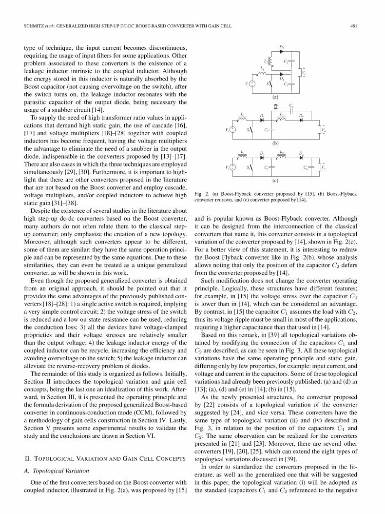
One of the first converters based on the Boost converter withcoupled inductor, illustrated in Fig. 2(a), was proposed by [15]
Fig. 2. (a) Boost-Flyback converter proposed by [15], (b) Boost-Flybackconverter redrawn, and (c) converter proposed by [14].
and is popular known as Boost-Flyback converter. Althoughit can be designed from the interconnection of the classicalconverters that name it, this converter consists in a topologicalvariation of the converter proposed by [14], shown in Fig. 2(c).For a better view of this statement, it is interesting to redrawthe Boost-Flyback converter like in Fig. 2(b), whose analysisallows noting that only the position of the capacitor C2 defersfrom the converter proposed by [14].
Such modification does not change the converter operatingprinciple. Logically, these structures have different features;for example, in [15] the voltage stress over the capacitor C2
is lower than in [14], which can be considered an advantage.By contrast, in [15] the capacitor C1 assumes the load with C2,thus its voltage ripple must be small in most of the applications,requiring a higher capacitance than that used in [14].
Based on this remark, in [39] all topological variations ob-tained by modifying the connection of the capacitors C1 andC2 are described, as can be seen in Fig. 3. All these topologicalvariations have the same operating principle and static gain,differing only by few properties, for example: input current, andvoltage and current in the capacitors. Some of these topologicalvariations had already been previously published: (a) and (d) in[13]; (a), (d) and (e) in [14]; (b) in [15].
As the newly presented structures, the converter proposedby [22] consists of a topological variation of the convertersuggested by [24], and vice versa. These converters have thesame type of topological variation (ii) and (iv) described inFig. 3, in relation to the position of the capacitors C1 andC2. The same observation can be realized for the converterspresented in [21] and [23]. Moreover, there are several otherconverters [19], [20], [25], which can extend the eight types oftopological variations discussed in [39].
In order to standardize the converters proposed in the lit-erature, as well as the generalized one that will be suggestedin this paper, the topological variation (i) will be adopted asthe standard (capacitors C1 and C2 referenced to the negative

482 IEEE TRANSACTIONS ON CIRCUITS AND SYSTEMS—I: REGULAR PAPERS, VOL. 64, NO. 2, FEBRUARY 2017
Fig. 3. Topological variations proposed by [39].
Fig. 4. Topological variation i) of the converters proposed by: (a) [20]; (b) [22]and [24]; and (c) [25].
terminal of the input source Vi), as illustrated in Fig. 4 for theconverters proposed by [20], [22], [24], [25].
B. Gain Cell
From the standard topological variations shown in Fig. 4,it is possible to note great similarity between the diverseconverters presented in the literature. Indeed, only the circuitof the highlighted region is different for each topology. Suchcircuit is responsible for the additional voltage gain add tothe characteristic gain of the classical Boost converter and,therefore, will be called gain cell. In general, one can say thateach discussed converter is composed of a Boost converter, a
Fig. 5. Generalized boost converter with gain cell.
Fig. 6. Some gain cells.
TABLE IINDEXES a, b, c, AND p FOR THE GAIN CELLS
gain cell, and an output filter, as elucidated in Fig. 5. Theseresults indicate that the output voltage Vo of the generalizedconverter is given by (1), where VB is the output voltage of theconventional Boost converter, and Vgc is the additional voltageprovided by the gain cell.
Vo = VB + Vgc (1)
By reviewing some of the converters proposed in the litera-ture, it is possible to group the gain cells as shown in Fig. 6.These gain cells may be found in: I—[13]–[15]; III—[19];V—[20]; VI—[22] and [24]; VII—[25]; IX—[21] and [23]. Theothers were deduced by similarity.
Each of the gain cells present in Fig. 6 provides its ownvoltage given by
Vgc = aVa + bVb. (2)
The indexes a and b have specific values for each gain cell,as shown in Table I, and the voltages Va and Vb represent

SCHMITZ et al.: GENERALIZED HIGH STEP-UP DC-DC BOOST-BASED CONVERTER WITH GAIN CELL 483
Fig. 7. Secondary winding voltage at (a) CCM and (b) DCM.
the secondary winding voltage vL2, illustrated in Fig. 7 andexpressed by
Va =nVi (3)
Vb = −n(Vi − VB) (4)
where
n =
√L2
L1. (5)
Substituting (2), (3), (4) and the output voltage equation ofthe conventional Boost converter into (1), the static gain of thegeneralized converter at CCM operation can be obtained
MCCM =1 + an− (a− b)nD
1−D. (6)
A similar procedure can be done for the discontinuous-conduction mode (DCM), and in this case the static gain isgiven by
MDCM =1
2
[(1 + an) +
√(1 + an)2 +
4D2
K
](7)
where
K =2Lm
RoTs. (8)
When a converter operates in boundary-conduction mode(BCM), the voltage gain of CCM and DCM operation areequaled. Using (6) and (7), the critical value of the dimension-less parameter K can be expressed as
Kcrit =D(1−D)2
[1 + an− (a− b)nD] (1 + bn). (9)
If K is greater than Kcrit, the converter operates in CCM,otherwise it operates in DCM.
Through the topological variation and gain cell concepts, itverifies that many of the converters proposed in the literaturehave similar structures and can be represented by the samestatic gain equations in all the conduction modes. Therefore,throughout this paper, all these converters will be representedby a unique generalized converter: the Boost Converter withGain Cell (BCGC).
Fig. 8. Simplified switching model of the BCGC.
Fig. 9. (a) Stage 1 and (b) Stage 2 for the gain cell IX.
III. BOOST CONVERTER WITH GAIN CELL
The simplified switching model of the BCGC is illustratedin Fig. 8. The couple inductor is represented by an ideal trans-former with a magnetizing inductor Lm and a small leakageinductor Lk in the primary side [40]. Moreover, all the devicesare ideal and all the capacitors are large enough that theirvoltages can be considered constant in one switching period.
A. Operating Principle
The BCGC has five operating modes at continuous-conduction mode, excepting when it employs the gain cells Iand II, which have, respectively, only four and three operatingmodes; because these cells are particular cases, they will notbe discussed in this paper. Furthermore, due to differences inthe operation, the description of the operating modes will bedivided according to the polarity of the gain cell, classifiedin this work as positive or negative. Basically, the differenceof operation occurs in the conduction of the output diode D2.In some gain cells, the diode D2 is forward-biased during theperiod that the switch S1 is blocked (positive polarity), whereasin others, the diode D2 is forward-biased during the period thatthe switch S1 is in conduction (negative polarity).
In addition, when analyzing them separately, it is noted thatboth types of gain cells have two operating modes. In order thatthese modes are not confused with the operating modes of theentire converter, the operation of the gain cell is defined by twostages, exemplified in Fig. 9 and described as follows:
• Stage 1: with the aim to store energy, the capacitors Cgc1
(if any) of the gain cell are positioned in parallel withthe series connection of the secondary winding of thecoupled inductor and/or the capacitors Cgc2 (if any), asexemplified in Fig. 9(a);
• Stage 2: so that the energy transfer to the load can beperformed, the capacitors Cgc1 (if any) are positioned inseries with the secondary winding of the coupled inductor,while the capacitors Cgc2 (if any) are allocated in parallelwith such winding in order to store energy, as illustratedin Fig. 9(b).

484 IEEE TRANSACTIONS ON CIRCUITS AND SYSTEMS—I: REGULAR PAPERS, VOL. 64, NO. 2, FEBRUARY 2017
Fig. 10. Operating modes of the BCGC with positive polarity at CCM:(a) Mode 1, (b) Mode 2, (c) Mode 3, (d) Mode 4, and (e) Mode 5.
Fig. 11. Main waveforms of the BCGC at CCM for gain cells with (a) positivepolarity and (b) negative polarity.
It should be noted that the definition of both the operatingstages related to the gain cells facilitates the description of theoperating modes of the BCGC.
1) Positive Polarity Gain Cells: The gain cells I, III, V, VII,and IX depicted in the Fig. 6 are included in this group. Theoperating modes are described below and illustrated in Fig. 10,while the main waveforms are shown in Fig. 11(a); secondary
waveforms can be easily derived from the presented ones.These specific waveforms illustrated in Fig. 11 were obtainedfrom the standard topological variation i), but, they are alsovalid for any other topological variation of Fig. 3.
• Mode 1 (t0 < t < t1): in the first mode, illustrated inFig. 10(a), the switch S1 was turned on for a span andthe magnetizing inductor Lm and the leakage inductorLk are charged by the input voltage source Vi. The gaincell is in the Stage 1, thus, part of the energy from theinput source Vi is transferred to the gain cell through thecoupled inductor to charge its capacitors Cgc1 (if any).The diode D2 is reverse-biased, because the secondarywinding voltage is equal to Va, and the load Ro is sus-tained by the capacitor C2. This mode ends when theswitch S1 is turned off.
• Mode 2 (t1 < t < t2): with the blocking of the switchS1, the diode D1 is turned on. Thus, the energy storedin the leakage inductor is transferred to the capacitor C1.The gain cell remains in Stage 1, while the magnetizinginductor Lm continues to receive energy from the inputsource Vi and the diode D2 remains blocked. This modeis shown in Fig. 10(b) and ends when the current iLk
becomes equal to the current iLm.• Mode 3 (t2 < t < t3): when the current iLk becomes
equal to the current iLm, the current i2 in the secondarywinding of the coupled inductor becomes null. The gaincell starts to operate in Stage 2 and the output diode D2
is forward-biased, since the secondary winding voltage isnow given by −Vb. Thereby, the capacitors Cgc1 (if any)of the gain cell, the input source Vi, and the primary andsecondary windings of the coupled inductor are providingtheir energy to the capacitor C2 and to the load Ro.Furthermore, the capacitorC1 continues being charged bythe energy stored in the leakage inductor Lk, as shown inFig. 10(c). This mode ends when the energy stored in Lk
is depleted, i.e., when the current iLk becomes null.• Mode 4 (t3 < t < t4): with the end of the energy stored
in the leakage inductor Lk, the diode D1 is blocked. Thegain cell continues in Stage 2. The capacitors Cgc1 (ifany), the capacitor C1, and the secondary winding of thecoupled inductor remain providing their energy to thecapacitor C2 and to the load Ro. This mode is presentedin Fig. 10(d) and ends when the switch S1 is turned on.
• Mode 5 (t4 < t < t5): at the time t = t4, the switch S1
is turned on. Because the rising rate of the current iLk
is limited by the leakage inductor Lk, the switch S1 isturned on under zero-current switching (ZCS). Moreover,the gain cell continues in Stage 2, then, the capacitor Cgc1
(if any), the capacitor C1, and the secondary windingof the coupled inductor remain providing energy to thecapacitor C2 and to the load Ro, as shown in Fig. 10(e).This mode ends when iLk becomes equal to iLm, i.e., i2becomes null.
2) Negative Polarity Gain Cells: The gain cells II, IV, VI,VIII, and X of Fig. 6 are included in this group. The operatingmodes of the Boost converter with negative polarity gain cellwill not be described in this work due to the great similarity

SCHMITZ et al.: GENERALIZED HIGH STEP-UP DC-DC BOOST-BASED CONVERTER WITH GAIN CELL 485
Fig. 12. Key waveforms of the BCGC at CCM ignoring the transitory operat-ing modes.
with the previous case. Basically, while the positive gain cell isin the Stage 1, the negative gain cell is in the Stage 2, and viceversa. The main waveforms of the BCGC with negative polarityare shown in Fig. 11(b).
B. Formula Derivation
Since the operating principle and the main waveforms are al-ready known, one can calculate the key equations that describethe converter operation. For this, it will be considered that theleakage inductance is insignificant, becoming the modes 2 and5 despicable. Thus, only the modes 1, 3, and 4 are considered,as shown in Fig. 12, where the times tc and tx are defined as
tc �DTs (10)
tx �DxTs. (11)
The mean value of the primary winding current is directobtained by the static gain of the converter, as shown in (12).In contrast, by inspection, the mean value of the secondarywinding current can be described by (13), where Io representsthe mean value of the output current io.
I1 =MIo (12)
I2 =(b− a)Io (13)
Although the coupled inductor can be modeled similarly to atransformer, it is primarily a device for energy storage, whereasthe transformer is a device for power transfer [40]. For thisreason, the mean value of the magnetizing current iLm can bedifferent from zero and in this case is given by
ILm = [M − (a− b)n] Io. (14)
Additionally, by the inductor current-voltage relationship,the maximum IM and minimum Im values of the current iLm
can be written as
IM = ILm +ΔILm (15)
Im = ILm −ΔILm (16)
where
ΔILm =DVi
2Lmfs. (17)
Since the average current through any capacitor, over oneswitching cycle, is zero in steady-state, one can observe, byinspection, that the mean values of the currents in all the diodesof the BCGC are equal to Io. Performing the calculation of theaverage current in the diode D1 and equaling it to Io, one canobtain (18). (Comparing Figs. 11 and 12 it is possible to notethat iD1 = i1 during the time interval tx).
Dx =2IoIM
(18)
Moreover, to calculate the stresses in all the components, it isimportant to find the values of the others parameters illustratedin Fig. 12, given by (19)–(22)
ILk =2(M − 1)Io
D− Im (19)
I2a =2ILm
n− 2(M − 1)Io
nD(20)
I2b =ImDx + IM (1 −D −Dx)
n(1−D)(21)
I2c =Imn
. (22)
As previously discussed, the difference between the gaincells with positive and negative polarities is the conductionperiod of the diode D2. In addition, as it can be seen inFig. 12, the current iD2 has the same waveform of the secondarywinding current i2 during the time that D2 conducts. Thisoccurs because it was considered that the current i2 is equallydivided among the diodes D2 and the diodes Dgc2 (if any).To solve these issues, two secondary indexes were created forthe gain cells: p indicates the polarity of the gain cell, and crepresents the number of diodes Dgc2 it have. With these twonew indexes it is possible to write generic equations (23)–(25)for the current in the diode D2:
ID2a = − I2a(1 + c)
(1− p)
2(23)
ID2b =I2b
(1 + c)
(1 + p)
2(24)
ID2c =I2c
(1 + c)
(1 + p)
2. (25)
The indexes c and p for the gain cells illustrated in Fig. 6 arealso presented in Table I.
A similar analysis can be done for the diodes Dgc1 and Dgc2
of the gain cells. Since the diodes Dgc2 share the current i2 withthe diodeD2, iD2 is equal to iDgc2. Conversely, the diodesDgc1
conduct by themselves the current i2 in the complementaryperiod, therefore, knowing the number of diodes Dgc1, givenby (a+ b)− (1 + c), it is simple to calculate the current iDgc1.
Finally, since all the current waveforms are piecewise linearfunctions, the root-mean-square (rms) values of the currents can

486 IEEE TRANSACTIONS ON CIRCUITS AND SYSTEMS—I: REGULAR PAPERS, VOL. 64, NO. 2, FEBRUARY 2017
be obtained as following (26)–(30), where D′ = 1−D −Dx
I1,rms
=
√D
3
(I2m + ImILk + I2Lk
)+
Dx
3I2M (26)
I2,rms
=
√D
3I22a +
Dx
3I22b +
D′
3(I22b + I2bI2c + I22c) (27)
IS1,rms
=
√D
3
(I2m + ImILk + I2Lk
)(28)
ID1,rms
=
√Dx
3I2M (29)
ID2,rms
=
√D
3I2D2a+
Dx
3I2D2b+· · ·+D′
3(I2D2b+ID2bID2c+I2D2c).
(30)
To complete the components stresses usually needed to theconverter design, the peak reverse voltage values over thesemiconductor devices are given by
VS1,D1 =1
1−DVi (31)
VD2,Dgc =n
1−DVi. (32)
In Section II it was mentioned the possibility of the topologi-cal variations of the Fig. 3 be extended for the BCGC indepen-dently of the employed gain cell. Although the equations herepresented were obtained by analyzing the standard topologicalvariation (i), all these equations are valid for the others topo-logical variations (ii)–(viii). In fact, only some properties aredifferent for distinct topological variations, as the input currentand the current and voltage at the capacitors C1 and C2. Theseproperties will be not formulated in this paper; however, theycan be easily obtained by the previous equations. Moreover, thetopological variations can be qualitatively compared by theseproperties as figures of merit [39], which gives a glimpse ofwhat topological variation is the most suitable for a particularapplication.
IV. GENERALIZED GAIN CELL
As discussed in Section II, some gain cells presented in theFig. 6 were extracted from works previously published in theliterature, commonly titled “novel high step-up dc-dc convert-ers.” However, all these converters can be understood as deriva-tions of the Boost converter with coupled inductor, initiallyproposed by [14]; it is just need to add voltage multiplier cellson the secondary of the referred inductor, in order to furtherincrease the static gain of the converter. Such voltage multipliercells are electrical circuits capable of generating a high dcvoltage from an ac voltage source. The most common cir-cuits are the Cockcroft-Walton multiplier [41] and the Dicksonmultiplier [42], both consisting of capacitor-diode pairs, differ-ing only in the connection mode, as can be seen in Fig. 13.
Fig. 13. (a) Cockcroft-Walton multiplier and (b) Dickson multiplier.
Fig. 14. Cockcroft-Walton multiplier for (a) upstream and (b) downstreamconnections; and (c) the four different generic cases obtain by the connectionwith the secondary winding of the coupled inductor.
In this work only the Cockcroft-Walton voltage multiplier(CWVM) will be considered, although a similar analysis canbe performed for the Dickson voltage multiplier.
A. Cockcroft-Walton-Based Gain Cells
In the construction of a gain cell, the voltage multipli-ers can be connected upstream—between the Boost converterand the secondary winding of the coupled inductor—anddownstream—between the secondary winding of the coupledinductor and the output filter. Furthermore, as shown in Fig. 14,for both (a) upstream and (b) downstream, there are two possi-bilities of connection with the secondary winding:
• DOT connected in 1 and non-DOT in 2;• DOT connected in 2 and non-DOT in 1;• DOT connected in 3 and non-DOT in 4;• DOT connected in 4 and non-DOT in 3.
Performing the combination of these connection possibili-ties, four different generic cases of gain cells using the CWVMare obtained and summarized in Fig. 14(c).
1) Case I: In the case I, the DOT of the secondary windingof the coupled inductor is connected in 1 and 3, while the non-DOT is connected in 2 and 4, generating the generic gain cellshown in Fig. 15. The sub-indexes of A and B, representedby NA and NB (ANA and BNB), match the number ofcapacitor-diode pairs that are used, respectively, upstream and
SCHMITZ et al.: GENERALIZED HIGH STEP-UP DC-DC BOOST-BASED CONVERTER WITH GAIN CELL 487
Fig. 15. Generic gain cell with CWVM for the case I.
Fig. 16. (a) Positive polarity gain cell and (b) negative polarity gain cell.
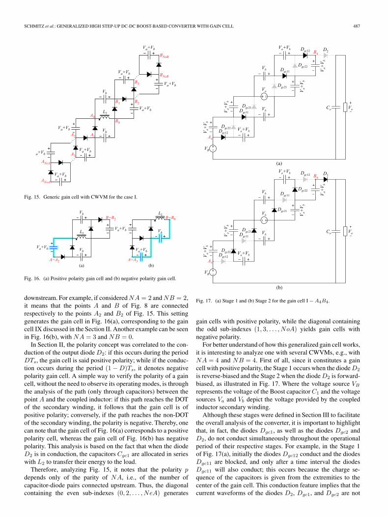
downstream. For example, if consideredNA = 2 andNB = 2,it means that the points A and B of Fig. 8 are connectedrespectively to the points A2 and B2 of Fig. 15. This settinggenerates the gain cell in Fig. 16(a), corresponding to the gaincell IX discussed in the Section II. Another example can be seenin Fig. 16(b), with NA = 3 and NB = 0.
In Section II, the polarity concept was correlated to the con-duction of the output diode D2: if this occurs during the periodDTs, the gain cell is said positive polarity; while if the conduc-tion occurs during the period (1 −D)Ts, it denotes negativepolarity gain cell. A simple way to verify the polarity of a gaincell, without the need to observe its operating modes, is throughthe analysis of the path (only through capacitors) between thepoint A and the coupled inductor: if this path reaches the DOTof the secondary winding, it follows that the gain cell is ofpositive polarity; conversely, if the path reaches the non-DOTof the secondary winding, the polarity is negative. Thereby, onecan note that the gain cell of Fig. 16(a) corresponds to a positivepolarity cell, whereas the gain cell of Fig. 16(b) has negativepolarity. This analysis is based on the fact that when the diodeD2 is in conduction, the capacitors Cgc1 are allocated in serieswith L2 to transfer their energy to the load.
Therefore, analyzing Fig. 15, it notes that the polarity pdepends only of the parity of NA, i.e., of the number ofcapacitor-diode pairs connected upstream. Thus, the diagonalcontaining the even sub-indexes (0, 2, . . . , NeA) generates
Fig. 17. (a) Stage 1 and (b) Stage 2 for the gain cell I −A4B4.
gain cells with positive polarity, while the diagonal containingthe odd sub-indexes (1, 3, . . . , NoA) yields gain cells withnegative polarity.
For better understand of how this generalized gain cell works,it is interesting to analyze one with several CWVMs, e.g., withNA = 4 and NB = 4. First of all, since it constitutes a gaincell with positive polarity, the Stage 1 occurs when the diodeD2
is reverse-biased and the Stage 2 when the diode D2 is forward-biased, as illustrated in Fig. 17. Where the voltage source VB
represents the voltage of the Boost capacitor C1 and the voltagesources Va and Vb depict the voltage provided by the coupledinductor secondary winding.
Although these stages were defined in Section III to facilitatethe overall analysis of the converter, it is important to highlightthat, in fact, the diodes Dgc1, as well as the diodes Dgc2 andD2, do not conduct simultaneously throughout the operationalperiod of their respective stages. For example, in the Stage 1of Fig. 17(a), initially the diodes Dgc12 conduct and the diodesDgc11 are blocked, and only after a time interval the diodesDgc11 will also conduct; this occurs because the charge se-quence of the capacitors is given from the extremities to thecenter of the gain cell. This conduction feature implies that thecurrent waveforms of the diodes D2, Dgc1, and Dgc2 are not

488 IEEE TRANSACTIONS ON CIRCUITS AND SYSTEMS—I: REGULAR PAPERS, VOL. 64, NO. 2, FEBRUARY 2017
TABLE IIINDEXES a, b, c, AND p FOR DIFFERENT COMBINATIONS OF
CAPACITOR-DIODE PAIRS FOR THE CASE I
TABLE IIIINDEXES a, b, c, AND p FOR GENERIC COMBINATIONS FOR THE CASE I
exactly equal to those indicated in Section III; despite beinga reasonable approximation. Basically, the larger is the gaincell, more the current in these diodes differs from the simplifiedanalysis realized in Section III. However, considering that thecapacitors are large enough that their voltage can be consideredconstant, it will not affect the voltage gain provided by the gaincell. From Fig. 17(b) one can conclude that, in this case, thevoltage referred to the gain cell is given by (33), i.e., this gaincell presents the indexes a = 4 and b = 5 [see (2)]. Performingthe same analysis for different gain cells of Fig. 15, it is possibleto generate the Table II.
Vgc = Vo − VB = 4Va + 5Vb (33)
By the Table II it is observed that all capacitor-diode pairsare used only when NA and NB have the same parity. Thisstatement can be represented by (34), wherein the number 1(one) corresponds to the voltage gain provided by the coupledinductor itself.
a+ b = NA+NB + 1 (34)
In situations where the parities of NA and NB are different,one of the capacitor-diode pairs becomes irrelevant to thevoltage gain and hence (34) becomes (35). Such gain cellsmust be avoided, since they increase cost, volume and lossesunnecessarily.
a+ b = (NA+NB − 1) + 1 (35)
From Table II is also possible to observe that for this setting
b = a+ 1. (36)
Thus, in possession of (34)–(36), one can find the genericvalues of the indexes a and b presented in Table III, so that NeAand NeB represent even numbers while NoA and NoB oddnumbers. Moreover, this table also exposes the index c in itsgeneric form for the case I, obtained by inspection.
Fig. 18. Generic gain cell with CWVM for the case II.
TABLE IVINDEXES a, b, c, AND p FOR GENERIC COMBINATIONS FOR THE CASE II
2) Case II: In this second case, illustrated in Fig. 18, theDOT of the secondary winding is connected in 2 and 4, whilethe non-DOT is connected in 1 and 3. As in the previous case,the polarity p only depends of the parity of NA. However, now,the diagonal containing the odd sub-indexes (1, 3, . . . , NoA)generates cells with positive polarity, whereas the diagonalcontaining even sub-indexes (0, 2, . . . , NeA) originates cellswith negative polarity.
Following the same procedure previously adopted from atable similar to Table II generated for the case I, one can noteagain that all the capacitor-diode pairs are used only when NAand NB have the same parity, attending (34). When NA andNB have different parities, one of the capacitor-diode pairsbecomes disposable and (35) is satisfied. In addition, observingsuch table, it follows that in case II the relation between a andb is given by (37). Thus, by (34), (35) and (37) it can determinethe generic indexes a and b according to Table IV. The index chas the same previous behavior.
a = b+ 1 (37)
3) Case III: For the case III the DOT of the secondary wind-ing is connected in 1 and 4, while the non-DOT is connectedin 2 and 3, as illustrated in Fig. 19. By having the sameupstream connection of the case I, the diagonal containing evensub-indexes (0, 2, . . . , NeA) generates gain cells with positive

SCHMITZ et al.: GENERALIZED HIGH STEP-UP DC-DC BOOST-BASED CONVERTER WITH GAIN CELL 489
Fig. 19. Generic gain cell with CWVM for the case III.
TABLE VINDEXES a, b, c, AND p FOR GENERIC COMBINATIONS FOR THE CASE III
polarity, whereas the diagonal containing odd sub-indexes(1, 3, . . . , NoA) gives cells with negative polarity. Unlike theprevious cases, in the case III all capacitor-diode pairs areavailed only when NA and NB have different parities. WhenNA and NB have equal parities, one of the capacitor-diodepairs does not influence the converter static gain. Moreover, inthis case, the relation between a and b is given by (38), thus, by(34), (35) and (38), it can determine the generic indexes a and baccording to Table V.
a = b (38)
4) Case IV: In the fourth and last case, presented in Fig. 20,the DOT of the secondary winding is connected in 2 and 3,while the non-DOT is connected in 1 and 4. Since this isthe same upstream connection of the case II, the diagonalcontaining the odd sub-indexes (1, 3, . . . , NoA) generates gaincells with positive polarity, whereas the diagonal containingeven sub-indexes (0, 2, . . . , NeA) gives cells with negativepolarity. As in the case III, all capacitor-diode pairs are availedonly when NA and NB have different parities, in addition, therelation between a and b is also given by (37). Thereby, thegeneric indexes for the case IV are presented in Table VI.
B. Gain Cells Comparison Analysis
Throughout this work the gain cells were represented by theirindexes (a, b, c, and p) and all the equations that describes the
Fig. 20. Generic gain cell with CWVM for the case IV.
TABLE VIINDEXES a, b, c AND p FOR GENERIC COMBINATIONS FOR THE CASE IV
operation of the BCGC at CCM were obtained as function ofthese indexes, principally the indexes a and b. (the secondaryindexes c and p are only related with the conduction of theoutput and gain cell diodes). From the four distinct cases basedon the CWVM one can conclude, by (36)–(38), that {a, b ∈N||a− b| ≤ 1}. With the knowledge of the values that theseindexes can achieve, it is possible to conduct some comparisonanalyses among the gain cells with different indexes a and b.
The variation of the static gain (7) with the duty cycle for gaincells with different indexes are illustrated in Fig. 21(a) undern = 3. From Fig. 21(a) it is possible to observe the relationbetween the static gain and the number of voltage multipliercells used, since they are directly related with the indexes a andb [see (34)]. In addition, it is verified that the index a has moreinfluence for D < 0.5, whereas the index b is predominant forD > 0.5. For this reason, a gain cell with a > b will present ahigher static gain for D < 0.5 and a lower static gain for D >0.5 than a gain cell with the same number of capacitor-diodepairs but with a < b.
In Fig. 21(b) is presented the critical value of the dimension-less parameter K (9), also for different gain cells and under n =3. From Fig. 21(b) it can note that this parameter Kcrit reduceswith the increase of number of capacitor-diode pairs. Thisbehavior indicates that, for indexes with higher values, a lowermagnetizing inductance Lm will be necessary for the converter
490 IEEE TRANSACTIONS ON CIRCUITS AND SYSTEMS—I: REGULAR PAPERS, VOL. 64, NO. 2, FEBRUARY 2017
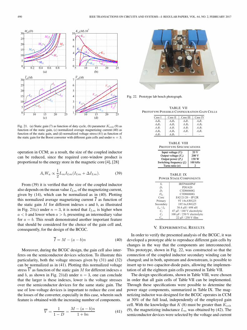
Fig. 21. (a) Static gain (7) as function of duty cycle, (b) parameter Kcrit (9) asfunction of the static gain, (c) normalized average magnetizing current (40) asfunction of the static gain, and (d) normalized voltage stress (41) as function ofthe static gain for the Boost converter with different gain cells and under n = 3.
operation in CCM; as a result, the size of the coupled inductorcan be reduced, since the required core-window product isproportional to the energy store in the magnetic core [4], [28]
AeWa ∝ 1
2LmILm(ILm +ΔILm). (39)
From (39) it is verified that the size of the coupled inductoralso depends on the mean value ILm of the magnetizing current,given by (14), which can be normalized as in (40). Plottingthis normalized average magnetizing current I as function ofthe static gain M for different indexes a and b, as illustratedin Fig. 21(c) under n = 3, it is noted that ILm is higher whena < b and lower when a > b, presenting an intermediary valuefor a = b. This result demonstrated another important featurethat should be considered for the choice of the gain cell and,consequently, for the design of the BCGC.
I = M − (a− b)n (40)
Moreover, during the BCGC design, the gain cell also inter-feres on the semiconductor devices selection. To illustrate thisparticularity, both the voltage stresses given by (31) and (32)can be normalized as in (41). Plotting this normalized voltagestress V as function of the static gain M for different indexes aand b, as shown in Fig. 21(d) under n = 3, one can concludethat the larger is these indexes, lower is the voltage stressesover the semiconductor devices for the same static gain. Theuse of low-voltage devices is important to reduce the cost andthe losses of the converter, especially in this case, wherein suchfeature is obtained with the increasing number of components.
V =1
1−D=
M − (a− b)n
1 + bn(41)
Fig. 22. Prototype lab bench photograph.
TABLE VIIPROTOTYPE POSSIBLE CONFIGURATION GAIN CELLS
TABLE VIIIPROTOTYPE SPECIFICATIONS
TABLE IXPOWER STAGE COMPONENTS
V. EXPERIMENTAL RESULTS
In order to verify the presented analysis of the BCGC, it wasdeveloped a prototype able to reproduce different gain cells bychanges in the way that the components are interconnected.This prototype, shown in Fig. 22, was constructed so that theconnection of the coupled inductor secondary winding can bechanged; and in both, upstream and downstream, is possible toinsert up to two capacitor-diode pairs, allowing the implemen-tation of all the eighteen gain cells presented in Table VII.
The design specifications, shown in Table VIII, were chosenin order that all gain cells of Table VII can be implemented.Through these specifications were possible to determine thepower stage components, summarized in Table IX. The mag-netizing inductor was designed for the BCGC operates in CCMat 30% of the full load, independently of the employed gaincell. With the knowledge that K (8) must be greater than Kcrit
(9), the magnetizing inductance Lm was obtained by (42). Thesemiconductor devices were selected by the voltage and current

SCHMITZ et al.: GENERALIZED HIGH STEP-UP DC-DC BOOST-BASED CONVERTER WITH GAIN CELL 491
Fig. 23. Static gain results of the Boost converter with different gain cells.
stresses described in Section III. Furthermore, it is important tohighlight that, as the prototype should allow the operation ofthe Boost converter with different gain cells, it was necessaryto consider the worst stresses that may arise, damaging theconverter performance and efficiency.
Lm >KcritTs
2
V 2o
0.3Po(42)
Fig. 23 presents the static gain results obtained for the Boostconverter with different gain cells in open-loop with a fixedresistive load (Ro = 270 Ω), where:
• MSLK—theoretical static gain without the influence ofthe leakage inductance of the coupled inductorgiven by(6);
• MCLK—theoretical static gain with the influence of theleakage inductance of the coupled inductor given by
MCCM =
1+an−(a−b)nD1−D
1 +[2(an)2
D2 +(bn2 − 1
) (1+bn)2
(1−D)2
]LkfsRo
;
(43)• MPSIM—static gain obtained through simulations in the
software PSIM using ideal components;• MSPICE—static gain obtained through simulations in the
software OrCAD EE PSpice using models provided by themanufactures of the employed components;
• MEXP—experimental static gain.
Due to the limitation of the function generator CFG253,used to generate the gate signal, the static gains were obtainedfor duty cycles greater than 20%. Thus, using 5% step, the
Fig. 24. (a) Experimental and simulated efficiency curves as function ofthe duty cycle with Ro = 270 Ω, and (b) experimental efficiency curves asfunction of the output power with M = 10 for different gain cells.
results for each gain cell was extracted up to the duty cycle thatmost closely approach the specified maximum output voltage(200 V), avoiding damage to the converter. The results pre-sented in Fig. 23 confirm that the static gain becomes largerwith the increase in the number of capacitor-diode pairs for agiven turns ratio n, despite being affected by the duty cycle lossand the converter efficiency.
The duty cycle loss can be observed by the MSLK andMPSIM curves, which indicates that converters with higherstatic gains are more impacted by this effect. This result isin accordance with the expression presented in (43) and herecalled MCLK, where it can be seen that the static gain decreaseswith the increase of the turns ratio n and/or the indexes a and b,especially for extreme values of duty cycles.
The difference between the MPSIM and MEXP curves givesan idea of the Boost converter efficiency with different gaincells. It is verified that with the increasing number of capacitor-diode pairs, MPSIM and MEXP become more distant, i.e., theconverter efficiency worsens gradually. To better observe suchefficiency reduction, the efficiency curves of the converter pro-totype were measured for some experiments of Fig. 23 by thepower analyzer WT500 and are depicted in Fig. 24(a), togetherwith the corresponding simulated efficiency results. In addition,Fig. 24(b) shows the typical experimental efficiency curves witha fixed static gain (M = 10) over a range of output power. Fromthese results it is confirmed that the efficiency of the converterprototype becomes lower with the increasing number of voltagemultiplier cells; which can be naturally justified, since a largeramount of components implies greater losses.
It emphasizes that the converter was designed so that allthe gain cells of Table VII can be implemented, damaging theconverter efficiency. For example, as seen in Fig. 21(d), theincreasing of voltage multipliers cells leads to lower voltagestresses over the semiconductor devices, however, this featurewas not availed in this prototype. If a prototype had been de-signed for each gain cell, the difference among these efficiencycurves could be at least alleviated. Nonetheless, despite theefficiency of the converter prototype be damaged by the designprocedure, one can verify from Fig. 24 that the BCGC canachieve high efficiencies (> 90%). Additionally, it is possibleto observe in previously published converters [20]–[24] that theBCGC can achieve efficiencies higher than 95% over a wideload range, reinforcing its high efficiency feature.

492 IEEE TRANSACTIONS ON CIRCUITS AND SYSTEMS—I: REGULAR PAPERS, VOL. 64, NO. 2, FEBRUARY 2017
Fig. 25. Experimental waveforms for the gain cells: (a) III − A1B0 (positivepolarity), and (b) III −A0B1 (negative polarity).
Another consequence of the increasing number of capacitor-diode pairs in the gain cell is the reduction of the reliability.Nevertheless, in recent years, the failure rates of power semi-conductor devices have been greatly reduced [43] and, in thecase of gain cells, ceramic or film capacitors can be used insteadof electrolytic ones. Such conditions may help the designedconverter to meet the reliability requirements for a particularapplication.
Lastly, Fig. 25 presents the input voltage vi, the Boost voltagevB , the output voltage vo, the voltage vS1 across the mainswitch, the primary i1 and the secondary i2 currents in thecoupled inductor, and the current iD2 in the output diode at halfload for both, positive polarity (III −A0B1) and negative po-larity (III −A1B0) gain cells. These experimental waveformsagree with the operating principle and the steady-state analysisdescribed in this work.
VI. CONCLUSION
This paper has demonstrated that many Boost-based convert-ers proposed in the literature have similar structures and can beanalyzed as a unique converter, here called: the Boost Converterwith Gain Cell. The principle of operation, the key waveformsand the components stresses of this converter were analyzed ina generalized way, independently of the employed gain cell. Inaddition, it was developed a methodology to create any gaincell through different connections between voltage multipliersand an inductor coupled to the Boost inductor. Based on thismethodology, it was developed a prototype able to operate witheighteen different gain cells, enabling the comparison amongtheoretical, simulated and experimental static gain results.
An interesting contribution of this work is the possibility toapply the gain cell concept as a design feature. For example, aquestion that may appear in a project for a particular applicationis whether is better to increase the transformer ratio of thecoupled inductor or to add another voltage multiplier cell. Thisis a classic optimization problem that is not easy to answer; itwill depend of several variables and the desired characteristicsof the project. However, with the generalized analysis heredeveloped, the gain cell can be used as a freedom degree in opti-mization designs together with the classical ones (for example:the switching frequency, the turns ratio, as well as, the electricalcomponents and materials) and thereby that question will beautomatically answered through the optimization algorithm.
Despite the gain cell concept was derived through Boost-based converters, this concept can be applied in other classicaldc-dc converters, resulting in novel high step-up topologies.Moreover, as shown before, several others non-isolated highstep-up high efficiency dc-dc converters have been proposedrecently. Since these converters are usually based on the sameconverters and using the congenerous high step-up techniques,one can conclude that probably some of these converters canalso be treated as a unique converter and an analysis similar tothe one proposed by this paper can be realized.
REFERENCES
[1] W. Li and X. He, “Review of nonisolated high-step-up dc/dc convertersin photovoltaic grid-connected applications,” IEEE Trans. Ind. Electron.,vol. 58, no. 4, pp. 1239–1250, Apr. 2011.
[2] S. V. Araujo, R. P. Torrico-Bascope and G. V. Torrico-Bascope, “Highlyefficient high step-up converter for fuel-cell power processing based onthree-state commutation cell,” IEEE Trans. Ind. Electron., vol. 57, no. 6,pp. 1987–1997, Jun. 2010.
[3] M. Kasper, D. Bortis, and J. W. Kolar, “Classification and comparativeevaluation of PV panel-integrated dc-dc converter concepts,” IEEE Trans.Power Electron., vol. 29, no. 5, pp. 2511–2526, May 2014.
[4] R. W. Erickson and D. Maksimovic, Fundamentals of Power Electronics,2nd ed. Norwell, MA, USA: Kluwer, 2001.
[5] K.-B. Park, G.-W. Moon, and M.-J. Youn, “Nonisolated high step-upstacked converter based on boost-integrated isolated converter,” IEEETrans. Power Electron., vol. 26, no. 2, pp. 577–587, Feb. 2011.
[6] T.-F. Wu, and T.-H. Yu, “Unified approach to developing single-stagepower converters,” IEEE Trans. Aerosp. Electron. Syst., vol. 34, no. 1,pp. 211–223, Jan. 1998.
[7] F. L. Luo and H. Ye, “Positive output cascade boost converters,” IEE Proc.Electr. Power Appl., vol. 151, no. 5, pp. 590–606, Sep. 2004.
[8] Y. R. de Novaes, A. Rufer, and I. Barbi, “A new quadratic, three-level, dc/dc converter suitable for fuel cell applications,” in Proc. PowerConvers. Conf., Nagoya, Japan, 2007, pp. 601–607.
[9] M. Prudente, L. L. Pfitscher, G. Emmendoerfer, E. F. Romaneli, andR. Gules, “Voltage multiplier cells applied to non-isolated dc-dc con-verters,” IEEE Trans. Power Electron., vol. 23, no. 2, pp. 871–887,Mar. 2008.
[10] F. L. Luo and H. Ye, “Positive output super-lift converters,” IEEE Trans.Power Electron., vol. 18, no. 1, pp. 105–113, Jan. 2003.
[11] Y. Berkovich, A. Shenkmann, B. Axelrod, and G. Golan, “Structures oftransformerless step-up and step-down controlled rectifiers,” IET PowerElectron., vol. 1, no. 2, pp. 245–254, Jun. 2008.
[12] E. H. Ismail, M. A. Al-Saffar, A. J. Sabzali, and A. A. Fardoun, “A familyof single-switch PWM converter with high step-up conversion ratio,”IEEE Trans. Circuits Syst. I, Reg. Papers, vol. 55, no. 4, pp. 1159–1171,May 2008.
[13] Q. Zhao, F. Tao, Y. Hu, and F. C. Lee, “Active-clamp dc/dc convertersusing magnetic switches,” in Proc. IEEE Appl. Power Electron. Conf.,Anaheim, CA, USA, 2001, pp. 946–952.
[14] Q. Zhao and F. C. Lee, “High-efficiency, high step-up dc-dc converters,”IEEE Trans. Power. Electron., vol. 18, no. 1, pp. 65–73, Jan. 2003.
[15] K. C. Tseng and T. J. Liang, “Novel high-efficiency step-up converter,”IEE Proc. Elect. Power Appl., vol. 151, no. 2, pp. 182–190, Mar. 2004.

SCHMITZ et al.: GENERALIZED HIGH STEP-UP DC-DC BOOST-BASED CONVERTER WITH GAIN CELL 493
[16] S.-M. Chen, T.-J. Liang, L.-S. Yang, and J.-F. Chen, “A cascaded highstep-up dc-dc converter with single switch for microsource applications,”IEEE Trans. Power Electron., vol. 26, no. 4, pp. 1146–1153, Apr. 2011.
[17] M.-S. Lin, L.-S. Yang, and T.-J. Liang, “Study and implementation of asingle switch cascading high step-up dc-dc converter,” in Proc. IEEE Int.Conf. Power Electron./ECCE, Jeju, Korea, 2011, pp. 2565–2572.
[18] J.-W. Baek, M.-H. Ryoo, T.-J. Kim, D.-W. Yoo, and J.-S. Kim, “Highboost converter using voltage multiplier,” in Proc. Annu. Conf. IEEE Ind.Electron. Soc., 2005, pp. 567–572.
[19] Y. Zhao, W. Li, Y. Deng, X. N. He, S. Lambert, and V. Pickert, “Highstep-up boost converter with coupled inductor and switched capacitor,” inProc. IET PEMD, 2010, pp. 1–6.
[20] Y.-P. Hsieh, J.-F. Chen, T.-J. Liang, and L.-S. Yang, “A novel high step-up dc-dc converter for a microgrid system,” IEEE Trans. Power Electron.,vol. 26, no. 4, pp. 1127–1136, Apr. 2011.
[21] Y.-P. Hsieh, J.-F. Chen, T.-J. Liang, and L.-S. Yang, “Novel high step-updc-dc converter with coupled-inductor and switched-capacitor techniquesfor a sustainable energy system,” IEEE Trans. Power Electron., vol. 26,no. 12, pp. 3481–3490, Dec. 2011.
[22] T.-J. Liang, S.-M. Chen, L.-S. Yang, J.-F. Chen, and A. Ioinovici, “Ultra-large gain step-up switched-capacitor dc-dc converter with coupled induc-tor for alternative sources of energy,” IEEE Trans. Circuits Syst. I, Reg.Papers, vol. 59, no. 4, pp. 864–874, Apr. 2012.
[23] Y.-P. Hsieh, J.-F. Chen, T.-J. Liang, and L.-S. Yang, “Novel high step-up dc-dc converter with coupled-inductor and switched-capacitor tech-niques,” IEEE Trans. Ind. Electron., vol. 59, no. 2, pp. 998–1007,Feb. 2012.
[24] Y.-P. Hsieh, J.-F. Chen, T.-J. Liang, and L.-S. Yang, “Novel high step-up dc-dc converter for distributed generation system,” IEEE Trans. Ind.Electron., vol. 60, no. 4, pp. 1473–1482, Apr. 2013.
[25] Y. Berkovich and B. Axelrod, “High step-up dc-dc converter based onthe switched-coupled-inductor boost converter and diode-capacitor multi-plier,” in Proc. IET PEMD, 2012, pp. 1–5.
[26] R.-J. Wai and R.-Y. Duan, “High step-up converter with coupled-inductor,” IEEE Trans. Power Electron., vol. 20, no. 5, pp. 1025–1035,Sep. 2005.
[27] B. Gu, J. Dominic, J.-S. Lai, Z. Zhao, and C. Liu, “High boost ratiohybrid transformer dc-dc converter for photovoltaic module applications,”in Proc. IEEE APEC, 2012, pp. 598–606.
[28] B. Gu, J. Dominic, B. Chen, L. Zhang, and J.-S. Lai, “Hybrid transformerZVS/ZCS dc-dc converter with optimized magnetics and improved powerdevices utilization for photovoltaic module applications,” IEEE Trans.Power Electron., vol. 30, no. 4, pp. 2127–2136, Apr. 2015.
[29] S.-M. Chen, T.-J. Liang, L.-S. Yang, J.-F. Chen, and K.-C. Juang, “Aquadratic high step-up dc-dc converter with voltage multiplier,” in Proc.IEEE IEMDC, 2011, pp. 1025–1029.
[30] X. Hu and C. Gong, “A high voltage gain dc-dc converter integratingcoupled-inductor and diode-capacitor techniques,” IEEE Trans. PowerElectron., vol. 29, no. 2, pp. 789–800, Feb. 2014.
[31] R. Gules, W. M. dos Santos, F. A. dos Reis, E. F. R. Romaneli, andA. A. Badin, “A modified SEPIC converter with high static gain forrenewable applications,” IEEE Trans. Power Electron., vol. 29, no. 11,pp. 5860–5871, Nov. 2014.
[32] Y. Deng, Q. Rong, W. Li, Y. Zhao, J. Shi, and X. He, “Single-switch highstep-up converters with built-in transformer voltage multiplier cell,” IEEETrans. Power Electron., vol. 27, no. 8, pp. 3557–3567, Aug. 2012.
[33] C.-H. Yeh, Y.-P. Hsieh, and J.-F. Chen, “A novel high step-up dc-dc con-verter with zero dc bias current coupled-inductor for microgrid system,”in Proc. IEEE IFEEC, 2013, pp. 388–394.
[34] I. Laird and D. D.-C. Lu, “High step-up dc/dc topology and MPPTalgorithm for use with a thermoelectric generator,” IEEE Trans. PowerElectron., vol. 28, no. 7, pp. 3147–3157, Jul. 2013.
[35] K.-C. Tseng and C.-C. Huang, “Ultra high step-up converters with re-duced diode stresses sharing,” in Proc. IEEE ISNE, 2013, pp. 531–516.
[36] R.-J. Wai, C.-Y. Lin, R.-Y. Duan, and Y.-R. Chang, “High-efficiency dc-dcconverter with high voltage gain and reduced switch stress,” IEEE Trans.Ind. Electron., vol. 54, no. 1, pp. 354–364, Feb. 2007.
[37] S.-K. Changchien, T.-J. Liang, J.-F. Chen, and L.-S. Yang, “Novel highstep-up dc-dc converter for fuel cell energy conversion system,” IEEETrans. Ind. Electron., vol. 57, no. 6, pp. 2007–2017, Jun. 2010.
[38] K.-C. Tseng, M.-H. Tsai, and C.-Y. Chan, “Design of high step-up con-version circuit for fuel cell power supply system,” in Proc. IEEE ISNE,2013, pp. 506–509.
[39] D. M. Van de Sype, K. De Gusseme, B. Renders, A. P. Van den Boss-che, and J. A. Melkebeek, “A single switch boost converter with a highconversion ratio,” in Proc. IEEE APEC, 2005, pp. 1581–1587.
[40] A. F. Witulski, “Introduction to modeling of transformers and coupledinductors,” IEEE Trans. Power Electron., vol. 10, no. 3, pp. 349–357,May 1995.
[41] J. D. Cockcroft and E. T. S. Walton, “Experiments with high velocitypositive ions. (I) Further developments in the method of obtaining high-velocity positive ions,” in Proc. R. Soc. Lond. A, vol. 136, pp. 619–630,Jun. 1932.
[42] J. F. Dickson, “On-chip high-voltage generation in MNOS integratedcircuits using an improved voltage multiplier technique,” IEEE J. Solid-State Circuits, vol. 11, no. 3, pp. 374–378, Jun. 1976.
[43] S. Yang, A. Bryant, P. Mawby, D. Xiang, L. Ran, and P. Tavner, “Anindustry-based survey of reliability in power electronics converters,” IEEETrans. Ind. Appl., vol. 47, no. 3, pp. 1441–1451, May/Jun. 2011.
Lenon Schmitz (S’15) was born in Blumenau, SC,Brazil, in 1990. He received the B.S. and M.S. de-grees in electrical engineering from Federal Univer-sity of Santa Catarina, Florianópolis, SC, Brazil, in2012 and 2015, respectively. He is currently workingtoward the Ph.D. degree in electrical engineeringat the same university. His interest research areasinclude high-efficient power converters, design op-timization techniques and grid-connected systems.
Denizar C. Martins (M’88) was born in São Paulo,SP, Brazil, in 1955. He received the B.S and M.S. de-grees in electrical engineering from Federal Univer-sity of Santa Catarina (UFSC), Florianópolis, Brazil,in 1978 and 1981, respectively, and the Ph.D. degreein electrical engineering from Polytechnic NationalInstitute of Toulouse, Toulose, France, in 1986. Heis currently a Titular Professor with the Departmentof Electrical and Electronics Engineering, UFSC.His interest research areas include dc-dc and dc-acconverters, high-frequency soft commutation, power
factor correction and grid-connected photovoltaic systems.
Roberto F. Coelho (M’15) was born in Florianópolis,SC, Brazil, in 1982. He received the B.S., M.S.,and Ph.D. degrees from Federal University of SantaCatarina (UFSC), Florianópolis, Brazil, in 2006,2008, and 2013, respectively. He is currently anAdjunct Professor in the Department of Electricaland Electronics Engineering, UFSC. His interestsinclude power converters, control, maximum powerpoint tracker systems, grid-connected systems anddistributed generated systems.

本文献由“学霸图书馆-文献云下载”收集自网络,仅供学习交流使用。
学霸图书馆(www.xuebalib.com)是一个“整合众多图书馆数据库资源,
提供一站式文献检索和下载服务”的24 小时在线不限IP
图书馆。
图书馆致力于便利、促进学习与科研,提供最强文献下载服务。
图书馆导航:
图书馆首页 文献云下载 图书馆入口 外文数据库大全 疑难文献辅助工具