general purpose i/o board rb01s1
TRANSCRIPT

GENERAL PURPOSE I/O BOARD
RB01S1
USER MANUAL

PINE S.r.l. MANRB01S1E.VA
2/34 RB01S1 USER MANUAL
1. Features........................................ ...............................................................................3
2. Connectors, Connections and jumper setting ...... ...................................................3
3. Configuration and reading of the analogue inputs ..................................................7
4. Configuration and reading of the frequencies .... .....................................................7
5. Reading of supply voltage (Vs), digital inputs, analogue outputs, relay outputs .8
6. Technical features of inputs and outputs........ .........................................................8
7. Serial communication lines ...................... .................................................................9
8. Technical data.................................. .........................................................................11
9. Dimensions ...................................... .........................................................................12
10. Product codification ........................... ..................................................................12
11. CE Conformity .................................. .....................................................................12
12. MODBUS specifications valid on RB01S1 .......... ................................................13
13. Function Codes supported by RB01S1............. ..................................................13
14. RB01S1 Registers ............................... ..................................................................15
15. RB01S1: table of the addresses of the I/O Regis ters.........................................16
16. Function code (0x04 – Read Input Registers).... .................................................17
17. Function Code (0x10) – Write Multiple Registers ...............................................19
18. Function Code (0x01) – Read Coils .............. .......................................................22
19. Function Code (0x02) – Read Discrete Inputs .... ................................................23
20. Function Code (0x05) – Write Single Coil ....... ....................................................25
21. Exceptions on MODBUS protocol .................. .....................................................26
22. CANBUS proprietary protocol.................... ..........................................................27
23. Read Register .................................. ......................................................................28
24. Write Registers................................ ......................................................................30
25. Exception messages on CANBUS protocol.......... ..............................................32
PINE S.r.l. MANRB01S1E.VA
3/34 RB01S1 USER MANUAL
RB01S1 is a general purpose I/O board for applications in several fields like naval field, industrial field, building automation, factory automation. RB01S1 has two galvanically insulated communication lines, a standard RS485 and a CAN BUS. 1. Features
• 8 digital inputs with optical insulation
• 6 analogue inputs
• 2 inputs for frequency measurement
• 8 output relays with Common, NO and NC contacts (SP DT)
• 2 low power analogue outputs
• Galvanically insulated RS485 serial communication l ine
• Galvanically insulated CAN BUS serial communication line
• Power supply: 12/24 V DC (from 10 to 35V) and from 8 a 24 V AC 50/60 Hz
• DIN rail version (DIN EN 50022) or grey ABS box RB01S1 inputs and outputs are managed by the serial communication lines using the MODBUS RTU protocol over RS485 and by a proprietary open protocol (similar to MODBUS RTU) over CAN BUS. It is possible to use only one of the two serial lines or both. The serial lines are galvanically insulated by power supply and galvanically insulated one by the other. the following actions can be performed:
• read the logical level of the digital inputs (ON/OF F)
• read the value of the analogue inputs
• read the supply voltage (Vmax if power supply is AC )
• read the frequency / period in the dedicated inputs
• read the state of the relay outputs (ON/OFF)
• activate / deactivate the relays (ON/OFF)
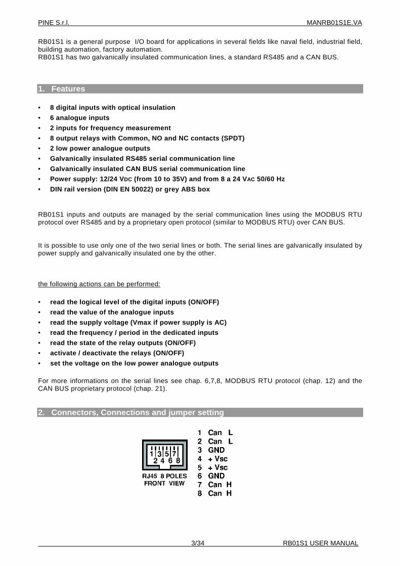
• set the voltage on the low power analogue outputs For more informations on the serial lines see chap. 6,7,8, MODBUS RTU protocol (chap. 12) and the CAN BUS proprietary protocol (chap. 21). 2. Connectors, Connections and jumper setting

PINE S.r.l. MANRB01S1E.VA
4/34 RB01S1 USER MANUAL
CONNECTORS AND CONNECTIONS

PINE S.r.l. MANRB01S1E.VA
5/34 RB01S1 USER MANUAL
LEGEND: ORL7 NC relay 7 normally closed contact ORL7 C relay 7 common contact ORL7 NC relay 7 normally open contact ORL6 NC relay 6 normally closed contact ORL6 C relay 6 common contact ORL6 NC relay 6 normally open contact ORL5 NC relay 5 normally closed contact ORL5 C relay 5 common contact ORL5 NC relay 5 normally open contact ORL4 NC relay 4 normally closed contact ORL4 C relay 4 common contact ORL4 NC relay 4 normally open contact ORL3 NC relay 3 normally closed contact ORL3 C relay 3 common contact ORL3 NC relay 3 normally open contact ORL2 NC relay 2 normally closed contact ORL2 C relay 2 common contact ORL2 NC relay 2 normally open contact ORL1 NC relay 1 normally closed contact ORL1 C relay 1 common contact ORL1 NC relay 1 normally open contact ORL0 NC relay 0 normally closed contact ORL0 C relay 0 common contact ORL0 NC relay 0 normally open contact
CAN BUS – 8 poles RJ45 connector for CAN BUS communication line +Vs power supply connection (positive pole for DC supply) -Vs power supply connection (common/negative pole DC supply) D IN0+ digital input 0 positive pole contact D IN0- digital input 0 negative pole contact D IN1+ digital input 1 positive pole contact D IN1- digital input 1 negative pole contact D IN2+ digital input 2 positive pole contact D IN2- digital input 2 negative pole contact D IN3+ digital input 3 positive pole contact D IN3- digital input 3 negative pole contact D IN4+ digital input 4 positive pole contact D IN4- digital input 4 negative pole contact D IN5+ digital input 5 positive pole contact D IN5- digital input 5 negative pole contact D IN6+ digital input 6 positive pole contact D IN6- digital input 6 negative pole contact D IN7+ digital input 7 positive pole contact D IN7- digital input 7 negative pole contact A IN0 analog input 0 A IN1 analog input 1 A IN2 analog input 2 A IN3 analog input 3 A IN4 analog input 4 A IN5 analog input 5 A OUT0 analog ouput 0 A OUT1 analog ouput 0 A GND zero voltage reference for analogue inputs and outputs and for frequency inputs F IN0 input 0 for frequency measurement F IN1 input 1 for frequency measurement RS485 COM RS485 common reference RS485 B connection to “B” of RS485 RS485 A connection to “A” of RS485

PINE S.r.l. MANRB01S1E.VA
6/34 RB01S1 USER MANUAL
JUMPER SETTING
JUMPER SETTING AS SUPPLIED BY MANUFACTURER Don’t change the position of these jumpers for a correct functioning of the product.
JP0 JP1 JP2 JP3 JP4 JP5 ,
JP6 JP7 JP8 J8
See the configuration of the inputs for setting the other jumpers. PINE S.r.l. is not responsible for malfunctioning or damaging to the board due to the wrong setting of the jumpers.
LEGENDA: open jumper
closed jumper (shortcircuited)

PINE S.r.l. MANRB01S1E.VA
7/34 RB01S1 USER MANUAL
3. Configuration and reading of the analogue inputs Every analogue input can be set, by jumpers, for reading a current, a resistance value or a voltage (this only on request). The input has to be read in the proper address that depends on the input configuration: INPUT CONFIGURATION ADDRESSES
current (from 0 to 25 mA) registers from 1280 to 1291 resistance (from 0 a 10 KΩ) registers from 1408 to 1419 voltage (from 0 to 10V) only on request register from 1152 to 1163
The values (10 bit) read by A/D converter of the board are available on the registers 1664 - 1675. The values read by A/D converter are adjusted using the internal voltage reference and they are available on the registers 1536 - 1547. Keep attention to the units! The units are available on the register’s table. The units are not related to the precision and to the resolution of the board reading. For the reading precision and resolution see the technical features chap. 6 and 8, data valid at 25° C. TABLE FOR ANALOGUE INPUTS CONFIGURATION (see chap. 2)
CURRENT RESISTANCE VOLTAGE NOTES AIN0 J0 J0 J0
For voltage reading install R71
AIN1 J1 J1 J1 For voltage reading install R70
AIN2 J2 J2 J2 For voltage reading install R69
AIN3 J3 J3 J3 For voltage reading install R68
AIN4 J4 J4 J4 For voltage reading install R67
AIN5 J5 J5 J5 For voltage reading install R63
4. Configuration and reading of the frequencies It is possible reading the frequency (in the registers 1920-1923) and the period (in the registers 2048-2051) of the signal at the inputs F IN0 / F IN1. The registers table shows the measure units. ATTENTION Keep attention to the units! The units are available on the register’s table. The units are not related to the precision and to the resolution of the board reading. For the reading precision and resolution see the technical features chap. 6 and 8, data valid at 25° C. TABLE FOR FREQUENCY INPUTS CONFIGURATION (see chap. 2)
Input from “W” signal of alternator
Input from magnetic pick-up
Input from PNP sender
Input from pick-up and check of line continuity
NOTE:
FIN0 J6
JP10
J6
JP10 J6
JP10
J6
JP10
Line continuity is not available for RB01S1.
FIN1 J7
JP11
J7
JP11
J7
JP11 J7
JP11
Line continuity is not available for RB01S1.

PINE S.r.l. MANRB01S1E.VA
8/34 RB01S1 USER MANUAL
5. Reading of supply voltage (Vs), digital inputs, analogue outputs, relay outputs No setting is required. See addresses table of the registers and the technical features. 6. Technical features of inputs and outputs
8 DIGITAL INPUTS
- optically coupled, insulation voltage 100 VAC - ON state voltage from 6,0 to 30,0 VDC or from 6 a 24 VAC - OFF state voltage from 0 to 1 VDC or from 0 a 0,7 VAC, or open circuit
6 ANALOGUE INPUTS
- not insulated, voltage is referred to negative pole of power supply (by the dedicated contact
A GND) - read by 10 bit A/D converter - Inputs selected by jumpers:
o current 0-25 mA (200 Ohm resistance to negative pole) this mean 0 V at 0 mA and 5 V at 25 mA current 4- 20 mA, 800 mV at 4 mA and 4,000V at 20 mA), accuracy: +/- 3 LSB or +/- 15mV
o voltage 0 – 10V (only on request), accuracy: +/- 3 LSB or +/- 15mV o resistance (with pull-up of 200 Ohm +/-1%):
o from 0 Ohm to 1 KOhm, accuracy: +/- 5 LSB or +/- 30mV or +/- 15 Ohm (at 1 KOhm) o from 1 KOhm a 10 KOhm, accuracy: +/- 5 LSB or +/- 30mV or +/- 450 Ohm (at 10 KOhm)
2 FREQUENCY INPUTS
- not insulated, voltage is referred to negative pole of power supply (by dedicated A GND) - low pass filter for band reducing and eliminating high frequency noise (for filtering short circuit
JP10 for FIN0 input, JP11 for FIN1 input - max measurable frequency without filtering: 10KHz - minimum time for low level and high level of signal - without filtering - 50 uS - max measurable frequency with filtering: 2KHz - minimum time for low level and high level of signal - with filtering - 250 uS - max measurable period: 2 seconds - minimum measurable voltage: 5 Vpp (peak to peak) - max input voltage: 90 Vpp (peak to peak) - accuracy: better than 0.1 % 8 OUTPUT RELAYS WITH N.OPEN AND N. CLOSED CONTACTS AVAILABLE (SPDT)
- contacts rating with resistive load:
o contact NO 12 A at 250 VAC and at 24 VDC o contact NC 8 A at 250 VAC and at 24 VDC o max switching power: 3000 VA on NO contact and 2000 VA on NC contact o max switching voltage: 400 VAC, 250Vdc
- Use fuses or equivalent devices for protecting rela y contacts and, for inductive loads use proper devices for avoiding dangerous overvoltages (the board has not protection devices).
2 ANALOGUE OUTPUTS
- not insulated - voltage range: 0-10V, max output settling time: 2 seconds over all the voltage range. - accuracy: +/- 0,5% of the set value on the registers + offset amplitude of +/- 25 mV. - load (to voltage reference A GND) >2 KOhm.
PINE S.r.l. MANRB01S1E.VA
9/34 RB01S1 USER MANUAL
SUPPLY VOLTAGE
- from 10 to 35 VDC , with polarity inversion protection - from 8 to 24 VAC - supply current at 12 VDC all the relays released: 50 mA - supply current at 24 VDC all the relays released: 30 mA - max supply current at 12 VDC all the relays excited: 450 mA - max supply current at 24 VDC all the relays excited: 250 mA
7. Serial communication lines
RS 485 PROTOCOL: MODBUS RTU (see pag 12), GALVANICALLY INSULATED LINE bit rate selected by dip switch (4 bit rate are available, as in BIT RATE SELECTION).
CAN BUS OPEN PROPRIETARY PROTOCOL similar to MODBUS RTU (see pag. 25), fixed bit rate at 250 Kbit/s, GALVANICALLY INSULATED LINE. BOARD ADDRESS An address between 0x11 and 0xF7 (with exception of address that have four zero in the lower bits of the address - this mean with exception of addresses 0x20, 0x30,…) may be assigned to the board. ADDRESS ASSIGNMENT Using the dip switch SW1 a new address can be assigned to the board (see ASSIGNEMENT VIA DIP SWITCH). Since only 4 switches are available for the 8 bit of address, the address assignment is done in two steps, 4 bit each time: the lower 4 bit and then the upper 4 bit or viceversa.
BIT RATE SELECTION (only for RS 485) Available bit rate: - 9600 bit/sec (switch 5,6,7,8 = 1000) in compliance with MODBUS spedification - 19200 bit/sec (switch 5,6,7,8 = 1001) in compliance with MODBUS spedification - 38400 bit/sec (switch 5,6,7,8 = 1010) not in compliance with MODBUS spedification - 57600 bit/sec (switch 5,6,7,8 = 1011) not in compliance with MODBUS spedification
SETTING VIA DIP SWITCH The dip switch SW1 is used for setting the BIT RATE and for assigning the board ADDRESS. Preset the new ADDRESS with the switches 5,6,7,8 and then confirm and store by switch 1 (see example in the next page). Preset the new BIT RATE with the switches 5,6,7,8 and then confirm and store by switch 2 (see example in the next page). Configuration sequence. Assignment of a new address: set in the switches 5,6,7,8 the lower 4 bit of the address then set the switch 1 ON and then OFF respecting the fig. 1 timing for the lower 4 bit; then set in the switches 5,6,7,8 the higher 4 bit of the address then set the switch 1 ON and then OFF respecting the fig. 1 timing for the higher 4 bit of the address. The same for the BIT RATE (only 4 bit are used): set in the switches 5,6,7,8 the new BIT RATE then set the switch 2 ON and then OFF respecting the fig. 1 timing. EXAMPLE OF ADDRESS AND BIT RATE SETTING Suppose you want to set the address 0xE3 = (E3)16 and BIT RATE 19200 bit/sec. ADDRESS 0xE3 is binary 1110 0011. “0” if the switch if in OFF position, ”1” if the switch is in ON position. With reference to 1 fig. - set the switches 5,6,7,8 in ON,ON,ON,OFF position and then confirm and store by switch 1 with the timing for storing the higher 4 bit of the ADDRESS - the switches 5,6,7,8 in OFF,OFF,ON,ON position and then confirm and store by switch 1 with the timing for storing the lower 4 bit of the ADDRESS .

PINE S.r.l. MANRB01S1E.VA
10/34 RB01S1 USER MANUAL
SET OF THE HIGHER 4 BIT OF THE BOARD ADDRESS
Set the higher 4 BIT (switch 1 is OFF) set switch 1 ON, wait for a time between 5 and 10 secon ds then switch 1 OFF |---------------------------------------------------|------------------------------------------------------|-------------------------|
SET OF THE LOWER 4 BIT OF THE BOARD ADDRESS
Set the lower 4 BIT (switch 1 is OFF) set swi tch 1 ON, wait for a time between 0,5 and 2,5 secon ds then switch 1 OFF |---------------------------------------------------|-------------------------------------------------------|-------------------------|
Fig. 1 BIT RATE 19200 bit/sec With reference to fig 2: - set the switches 5,6,7,8 in ON,OFF,OFF,ON position and then confirm and store by the switch 2 with the timing for storing the BIT RATE as in the following fig. 2
SET THE BIT RATE AT 19200 BIT/SEC
Set the bit rate at 19200 set switch 2 ON, wait for a time between 0,5 and 2,5 seconds then switch 2 OFF |---------------------------------------------------|--------------------------------------------------------|-------------------------| Fig. 2
PINE S.r.l. MANRB01S1E.VA
11/34 RB01S1 USER MANUAL
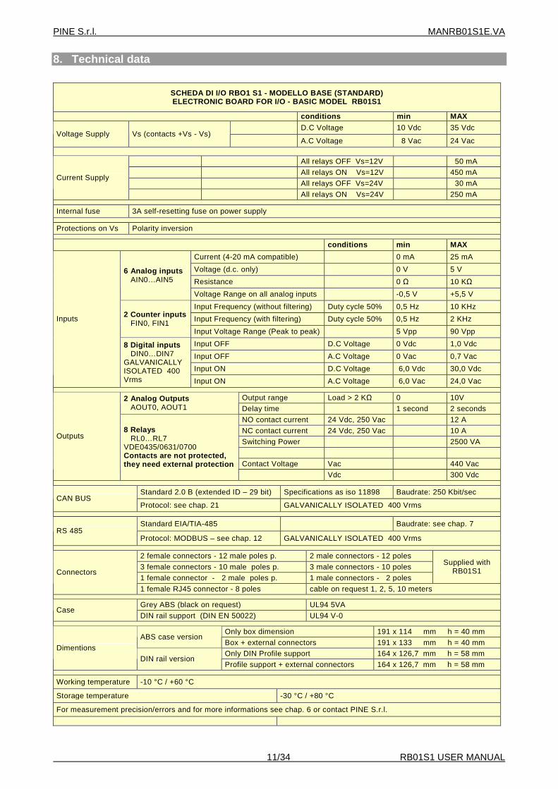
8. Technical data
SCHEDA DI I/O RBO1 S1 - MODELLO BASE (STANDARD) ELECTRONIC BOARD FOR I/O - BASIC MODEL RB01S1
conditions min MAX
D.C Voltage 10 Vdc 35 Vdc Voltage Supply Vs (contacts +Vs - Vs)
A.C Voltage 8 Vac 24 Vac
All relays OFF Vs=12V 50 mA
All relays ON Vs=12V 450 mA
All relays OFF Vs=24V 30 mA Current Supply
All relays ON Vs=24V 250 mA
Internal fuse 3A self-resetting fuse on power supply
Protections on Vs Polarity inversion
conditions min MAX
Current (4-20 mA compatible) 0 mA 25 mA
Voltage (d.c. only) 0 V 5 V
Resistance 0 Ω 10 KΩ 6 Analog inputs AIN0…AIN5
Voltage Range on all analog inputs -0,5 V +5,5 V
Input Frequency (without filtering) Duty cycle 50% 0,5 Hz 10 KHz
Input Frequency (with filtering) Duty cycle 50% 0,5 Hz 2 KHz 2 Counter inputs FIN0, FIN1
Input Voltage Range (Peak to peak) 5 Vpp 90 Vpp
Input OFF D.C Voltage 0 Vdc 1,0 Vdc
Input OFF A.C Voltage 0 Vac 0,7 Vac
Input ON D.C Voltage 6,0 Vdc 30,0 Vdc
Inputs
8 Digital inputs DIN0…DIN7 GALVANICALLY ISOLATED 400 Vrms Input ON A.C Voltage 6,0 Vac 24,0 Vac
Output range Load > 2 KΩ 0 10V 2 Analog Outputs AOUT0, AOUT1 Delay time 1 second 2 seconds
NO contact current 24 Vdc, 250 Vac 12 A
NC contact current 24 Vdc, 250 Vac 10 A
Switching Power 2500 VA
Contact Voltage Vac 440 Vac
Outputs 8 Relays RL0…RL7 VDE0435/0631/0700 Contacts are not protected, they need external protection
Vdc 300 Vdc
Standard 2.0 B (extended ID – 29 bit) Specifications as iso 11898 Baudrate: 250 Kbit/sec CAN BUS
Protocol: see chap. 21 GALVANICALLY ISOLATED 400 Vrms
Standard EIA/TIA-485 Baudrate: see chap. 7 RS 485
Protocol: MODBUS – see chap. 12 GALVANICALLY ISOLATED 400 Vrms
2 female connectors - 12 male poles p. 2 male connectors - 12 poles
3 female connectors - 10 male poles p. 3 male connectors - 10 poles
1 female connector - 2 male poles p. 1 male connectors - 2 poles
Supplied with RB01S1 Connectors
1 female RJ45 connector - 8 poles cable on request 1, 2, 5, 10 meters
Grey ABS (black on request) UL94 5VA Case
DIN rail support (DIN EN 50022) UL94 V-0
Only box dimension 191 x 114 mm h = 40 mm ABS case version
Box + external connectors 191 x 133 mm h = 40 mm
Only DIN Profile support 164 x 126,7 mm h = 58 mm Dimentions
DIN rail version Profile support + external connectors 164 x 126,7 mm h = 58 mm
Working temperature -10 °C / +60 °C
Storage temperature -30 °C / +80 °C
For measurement precision/errors and for more informations see chap. 6 or contact PINE S.r.l.

PINE S.r.l. MANRB01S1E.VA
12/34 RB01S1 USER MANUAL
9. Dimensions
ABS enclosure
DIN EN 50022 profile support
10. Product codification
SCHEDA DI I/O RBO1S - MODELLO BASE (STANDARD) ELECTRONIC BOARD FOR I/O - BASIC MODEL RB01S1
RB01 S1 X 01 A HW revision A series (Product family) SW revision 01 S1 Standard Version 1 ABS box P supporto per guida DIN D
11. CE Conformity
Il costruttore dichiara che le schede elettroniche della serie RB01 sono conformi ai requisiti di compatibilità elettromagnetica e di sicurezza secon do le direttiva 73/23/EEC, 89/336/EEC, 92/31/EEC, 93/68/EEC, 93/97/EEC ed EN 60945. The manufacturer declare that the electronic units of series RB01 are in conformity at requisition of electromagnetic compatibility and of security wi th directives 73/23/EEC, 89/336/EEC, 92/31/EEC and 93/68/EEC and 93/97/EEC and EN 60945 directives .

PINE S.r.l. MANRB01S1E.VA
13/34 RB01S1 USER MANUAL
RB01S1 MODBUS RTU PROTOCOL
Revision 1.0 RB01S1 is in compliance with MODBUS RTU protocol. In the following chapters there is the technical documentation for the serial communication RS485, as the “function code” list, the list of the “registers” and the measure resolutions and units. Many examples will help user for a quick start on using the board. User has to be familiar with MODBUS RTU protocol and terminology. The official documentation can be found on the web site http://www.modbus.org. Not all the timings are in accordance with standard timings of the MODBUS RTU so the user must use the timing of this manual. 12. MODBUS specifications valid on RB01S1 MODBUS protocol specifications:
Protocol MODBUS V 1.1b
MODBUS RTU OVER SERIAL LINE V1.02
Physic level EIA/TIA - 485 RS-485 a 2 wires + common
Bitrate 9600, 19200, 38400, 57600 bps (see note 1)
Parity Even
Stop bit 1
Frame timing > 10 ms
Delay from the bytes on a a frame < 5 ms
Available addresses 215 (see chap. 7) 1) The Error at 38400 bps (1.4%) and at 57600 bps (1.4%) is higher than 1% so these bit rates are not in accordance with the standard. 13. Function Codes supported by RB01S1 RB01S1 supports the following Function Codes:
Function Code Name Description
0x01 Read Coils Read the digital outputs (coil state)
0x02 Read Discrete Inputs Read the digital inputs
0x04 Read Input Registers Read Input Registers
0x05 Write Single Coil Write Single Coil
0x10 Write Multiple Registers Write Multiple Registers In black the recomended Function Codes. In case of reception of a not supported Function Code, RB01S1 generates an Exception. Notes and suggestions All the RB01S1 boards are “slaves”, the unit that operates with RB01S1 is said “master”. After a request (Function Code) master have to wait for the reply before sending another request. If after a while the slave does not reply (a timeout is recomended) the "master" can resubmit the request (Function Code) or signal the error to the user (generating an alarm) in order to solve the problem.

PINE S.r.l. MANRB01S1E.VA
14/34 RB01S1 USER MANUAL
The RB01C1 boards process also the broadcast messages (address 0x00), as required by the protocol. It’s not suggest to use it because it has few applications and no reply is expected. The examples will allow the use of RB01S1 in a short time. Flow chart and example in “C” language for CRC calculation. Flow Chart
CRC = 0xFFFF
CRC = CRC XOR BYTE
N = 0
CRC = CRC >> 1 (CRC SHIFT RIGHT)
Carry?
CRC = CRC XOR 0xA001
N = N + 1
Fine del messaggio?
FINE
N > 7 ?
SI
SI
SI
NO
NO
NO
BYTE = Prossimo
BYTE = Primo Byte

PINE S.r.l. MANRB01S1E.VA
15/34 RB01S1 USER MANUAL
Example in “C” language for CRC calculation unsigned int modbus_calc_crc(unsigned char *data, unsigned int size) unsigned int crc; unsigned int i; unsigned char carry; unsigned char n; crc = 0xFFFF; i = 0; while(size) crc = crc ^ data[i]; n = 0; do carry = crc & 0x01; crc >>= 1; if(carry) crc = crc ^ 0xA001; n++; while(n <= 7); i++; size--; return ( (crc&0xFF00)>>8 | (crc&0x00FF)<<8 );
14. RB01S1 Registers For representing each I/O (digital inputs, analogues output, …) RB01S1 uses a 32 bit unsigned variable. The size of a MODBUS register is 16 bit so each I/O variable of RB01S1 occupies two consecutive registers. The 16 MSbit of the variable are stored in the register with the lower address and the 16LSbit in the register with the higher address. The read/write operation have to be done by using the couple/s of registers containing the I/O variable/s. It is not possible the read/write operation on a single 16 bit register. We suggest to use the Function code (0x04) – Read Input Registers and the Function Code (0x10) – Write Multiple Registers for an easy access to the RB01S1 registers. Example 1 Suppose you want to read the supply voltage of the RB01S1 and that its value is 12.000V that is 12000 mV. With reference to the table of addresses (registers) in the chap. 15 this value is read from registers 1024 and 1025 as shown in the following table.
Registers Value
… …
1024 0x0000
1025 0x2EE0
… … 0x indicates that the number is in hexadecimal base. (00002EE0)16 = (12000)10 The registers 1024 and 1025 have to be read using one command. Any attempt for reading only the 1024 register or only the 1025 register will fail and RB01C1 will return an Exception.

PINE S.r.l. MANRB01S1E.VA
16/34 RB01S1 USER MANUAL
15. RB01S1: table of the addresses of the I/O Regis ters REGISTERS decimal REGISTERS hexadecimal I/O UNITS OPERATION DESCRIPTION
1024 - 1025 0x400 – 0x401 Vs mV Read Read the supply Voltage
1152 - 1153 0x480 – 0x481 AIN0 mV Read Reading of a Voltage 1154 - 1155 0x482 – 0x483 AIN1 1156 - 1157 0x484 – 0x485 AIN2 1158 - 1159 0x486 – 0x487 AIN3 1160 - 1161 0x488 – 0x489 AIN4 1162 - 1163 0x48A – 0x48B AIN5
1280 - 1281 0x500 – 0x501 AIN0 uA Read Reading of a Current 1282 - 1283 0x502 – 0x503 AIN1 1284 - 1285 0x504 – 0x505 AIN2 1286 - 1287 0x506 – 0x507 AIN3 1288 - 1289 0x508 – 0x509 AIN4 1290 - 1291 0x50A – 0x50B AIN5
1408 - 1409 0x580 – 0x581 AIN0 0.1 Ohm Read Reading of a Resistance 1410 - 1411 0x582 – 0x583 AIN1 1412 - 1413 0x584 – 0x585 AIN2 1414 - 1415 0x586 – 0x587 AIN3 1416 - 1417 0x588 – 0x589 AIN4 1418 - 1419 0x58A – 0x58B AIN5
1536 - 1537 0x600 – 0x601 AIN0 0.1 bit Read Read the bits of the A/D converter 1538 - 1539 0x602 – 0x603 AIN1 (compensated) 1540 - 1541 0x604 – 0x605 AIN2 1542 - 1543 0x606 – 0x607 AIN3 1544 - 1545 0x608 – 0x609 AIN4 1546 - 1547 0x60A – 0x60B AIN5
1664 - 1665 0x680 – 0x681 AIN0 0.1 bit Read Read the bits of the A/D converter 1666 - 1667 0x682 – 0x683 AIN1 (not compensated) 1668 - 1669 0x684 – 0x685 AIN2 1670 - 1671 0x686 – 0x687 AIN3 1672 - 1673 0x688 – 0x689 AIN4 1674 - 1675 0x68A – 0x68B AIN5
1792 - 1793 0x700 – 0x701 DIN0 OFF / ON Read State of the Digital Inputs 1794 - 1795 0x702 – 0x703 DIN1 1796 - 1797 0x704 – 0x705 DIN2 1798 - 1799 0x706 – 0x707 DIN3 If read as Input Registers: 1800 - 1801 0x708 – 0x709 DIN4 0x00000000 = OFF 1802 - 1803 0x70A – 0x70B DIN5 0x00000001 = ON 1804 - 1805 0x70C – 0x70D DIN6 1806 - 1807 0x70E – 0x70F DIN7
1920 - 1921 0x780 – 0x781 FIN0 0.01 Hz Read Frequency 1922 - 1923 0x782 – 0x783 FIN1
2048 - 2049 0x800 – 0x801 FIN0 0.1 us Read Period 2050 - 2051 0x802 – 0x803 FIN1
2304 - 2305 0x900 – 0x901 AOUT0 mV Read / Write Analogue Output Voltage 2306 - 2307 0x902 – 0x903 AOUT1
2432 - 2433 0x980 – 0x981 ORL0 OFF / ON Read / Write State of Digital Outputs 2434 - 2435 0x982 – 0x983 ORL1 2436 - 2437 0x984 – 0x985 ORL2 2438 - 2439 0x986 – 0x987 ORL3 If read as input registers: 2440 - 2441 0x988 – 0x989 ORL4 0x00000000 = OFF 2442 - 2443 0x98A – 0x98B ORL5 0x00000001 = ON 2444 - 2445 0x98C – 0x98D ORL6 2446 - 2447 0x98E – 0x98F ORL7

PINE S.r.l. MANRB01S1E.VA
17/34 RB01S1 USER MANUAL
16. Function code (0x04 – Read Input Registers) This function is used for registers reading. Message format:
Byte 0 Byte 1 Byte 2 Byte 3 Byte 4 Byte 5 Byte 6 Byte 7 Slave
Address Function
Code Starting Address
Quantity of Input Registers
CRC
Byte 0 – Slave Address Address of the slave board. Byte 1 – Function Code Function Code (0x04). Byte 2, Byte 3 – Starting Address Register Address –1 (as in MODBUS RTU). Byte 4, Byte 5 – Quantity of Input Registers Quantity of input registers to be read (two registers or a multiple of two, that is 4 byte or a multiple of 4 byte). Byte 6, Byte 7 – CRC CRC of the message. Format of the reply.
Byte 0 Byte 1 Byte 2 Byte 3 … Byte n Byte n+1 Byte n+2
Slave Address
Function Code
Byte Count Input Registers CRC
Byte 0 – Slave Address Slave address that sent the message. Byte 1 – Function Code Function Code (0x04). Byte 2 – Byte Count Amount of bytes sent containing the required Input Registers. The same amount of “Quantity of Input Registers” x 2 (because the unit is the byte). Byte 3 … Byte n – Input Registers Content of the Input Registers required, from the lowest register to the highest. Byte n+1, Byte n+2 CRC of the message.

PINE S.r.l. MANRB01S1E.VA
18/34 RB01S1 USER MANUAL
Example 2 Suppose you want to read the digital input DIN0 of the RB01S1 (the address of RB01S1 is 0xA1). With reference to the table of addresses (registers) in the chap. 15 this value is read in the registers 1792 and 1793 in decimal base that is 0x0700 and 0x0701 in exadecimal base. The byte 2 and 3 of the request will be 0x06 (byte 2) and 0xFF (byte 3) because 0x0700 – 1 = 0x06FF. If the DIN0 is “active” the content of the registers is:
Register Value
1792 (0x0700) 0x0000
1793 (0x0701) 0x0001
Summarizing, the Starting Address is: (1792 – 1)10 = (0700-1)16 = (06FF)16 = 0x06FF and the reading: 0x0000 in the register 1792 (0x0700) 0x0001 in the register 1793 (0x0701) Message format (request)
Byte 0 Byte 1 Byte 2 Byte 3 Byte 4 Byte 5 Byte 6 Byte 7 0xA1 0x04 0x06 0xFF 0x00 0x02 0x59 0xD3
Slave
Address Function
Code Starting Address
(register address - 1) Quantity of Input
Registers CRC
Reply
Byte 0 Byte 1 Byte 2 Byte 3 Byte 4 Byte 5 Byte 6 Byte 7 Byte 8
0xA1 0x04 0x04 0x00 0x00 0x00 0x01 0x9A 0x4E
Slave Address
Function Code
Byte count
Content of register 1792 (0x0700)
Content of register 1793 (0x0701)
CRC
If the input DIN0 is not “active”, the reading returns 0x0000 in the register 1792 and 0x0000 in the register 1793. Example 3 Suppose you want to read the voltage on the analogue input AIN0 and that this value is 1.250V. The address of RB01S1 is 0x81. With reference to the table of addresses (registers) in the chap. 15 this value is read in the registers 1152 and 1153 in decimal base that is 0x0480 and 0x0481 in exadecimal base. The content of the registers is:
Register Value 1152 (0x0480) 0x0000 1153 (0x0481) 0x04E2
Summarizing, the Starting Address is: (1152 – 1)10 = (0480-1)16 = (047F)16 = 0x047F and the reading: 0x0000 in the register 1152 (0x0480) 0x0E42 in the register 1153 (0x0481) that mean 0x 0000 04E2 = (1250)10 mV = 1.250V

PINE S.r.l. MANRB01S1E.VA
19/34 RB01S1 USER MANUAL
Message format (request)
Byte 0 Byte 1 Byte 2 Byte 3 Byte 4 Byte 5 Byte 6 Byte 7 0x81 0x04 0x04 0x7F 0x00 0x02 0x5E 0xE3
Slave
Address Function
Code Starting Address
(register address - 1) Quantity of Input
Registers CRC
Reply
Byte 0 Byte 1 Byte 2 Byte 3 Byte 4 Byte 5 Byte 6 Byte 7 Byte 8
0x81 0x04 0x04 0x00 0x00 0x04 0xE2 0xF8 0xC5
Slave Address
Function Code
Byte count
Content of register 1152 (0x0480)
Content of register 1153 (0x0481)
CRC
17. Function Code (0x10) – Write Multiple Registers The “Write Multiple Register” function is used for setting the value of one or more pairs of contiguous registers on RB01S1. Message format:
Byte 0 Byte 1 Byte 2 Byte 3 Byte 4 Byte 5 Byte 6 Byte 7 … Byte n Byte n+1 Byte n+2
Slave Address
Function Code
Starting Address
Quantity of Registers
Byte Count
Registers Value CRC
Byte 0 – Slave Address Address of the slave board. Byte 1 – Function Code Function Code (0x10). Byte 2, Byte 3 Starting Address Register Address – 1. Byte 4, Byte 5 - Quantity of Registers Quantity of the Registers to write. Byte 6 – Byte Count Quantities of bytes in the “Registers Value”. This is “Quantity of Registers” x 2 (because a registers need 2 bytes). Byte 7… Byte n – Registers Value Value to be written in the registers, from the lowest register to the highest. Byte n+1, Byte n+2 – CRC CRC of the message. Format of the reply:
Byte 0 Byte 1 Byte 2 Byte 3 Byte 4 Byte 5 Byte 6 Byte 7
Slave Address
Function Code
Starting Address Quantity of Registers CRC

PINE S.r.l. MANRB01S1E.VA
20/34 RB01S1 USER MANUAL
Byte 0 – Slave Address Slave address that sent the message. Byte 1 – Function Code Function Code (0x10). Byte 2, Byte 3 Starting Address Address from which you started writing – 1. Byte 4, Byte 5 – Quantity of Registers Amount of written registers. Byte 6, Byte 7 – CRC CRC of the message. Example 4 Suppose you want to set in the analogue output A OUT0 a voltage of 6.730V (6730 mV that is 0x0000 1A4A). The address of RB01S1 is 0x81. With reference to the table of addresses (registers) in the chap. 15 the number 0x0000 1A4A has to be written in the registers 2304 and 2305 in decimal base, 0x0900 and 0x0901 in exadecimal base. Summarizing, the Starting Address is: (2304 – 1)10 = (0900-1)16 = (08FF)16 = 0x08FF and the value to write in the registers is: 0x0000 in the register 2304 (0x900) 0x1A4A in the register 2305 (0x901) Message format (request)
Byte 0 Byte 1 Byte 2 Byte 3 Byte 4 Byte 5 Byte 6 Byte 7 Byte 8 Byte 9 Byte 10 Byte 11 Byte 12
0x81 0x10 0x08 0xFF 0x00 0x02 0x04 0x00 0x00 0x1A 0x4A 0xF8 0x3E
Slave
Address Function
Code Starting Address
Quantity of Registers
Byte Count Registers Value CRC
Reply
Byte 0 Byte 1 Byte 2 Byte 3 Byte 4 Byte 5 Byte 6 Byte 7 0x81 0x10 0x08 0xFF 0x00 0x02 0x6C 0x58
Slave
Address Function
Code Starting Address Quantity of Registers CRC
Example 5 Suppose you have to use the contacts ORL0_NO and ORL0_C, ORL2_NC and ORL2_C, ORL5_NO and ORL5_C for activating / deactivating the loads. First you want activate the relays ORL0, ORL2, ORL5 of the board RB01S1 with address 0x82. It is possible to use the Function Code 0x10 three time, one time for RL0 relay, one time for RL2 relay and one time for RL5 relay.

PINE S.r.l. MANRB01S1E.VA
21/34 RB01S1 USER MANUAL
ORL0: With reference to the table of addresses (registers) in the chap. 15 you have to write 0x0000 in the register 2432 (0x0980) and 0x0001 in the register 2433 (0x0981). Summarizing, the Starting Address is: (2432 – 1)10 = (0980-1)16 = (097F)16 = 0x097F and the value to write in the registers is: 0x0000 in the register 2432 (0x0980) 0x0001 in the register 2433 (0x0981) Message format (request)
Byte 0 Byte 1 Byte 2 Byte 3 Byte 4 Byte 5 Byte 6 Byte 7 Byte 8 Byte 9 Byte 10 Byte 11 Byte 12
0x82 0x10 0x09 0x7F 0x00 0x02 0x04 0x00 0x00 0x00 0x01 0xB9 0xDD
Slave
Address Function
Code Starting Address
Quantity of Registers
Byte Count
Registers Value CRC
Reply
Byte 0 Byte 1 Byte 2 Byte 3 Byte 4 Byte 5 Byte 6 Byte 7 0x82 0x10 0x09 0x7F 0x00 0x02 0x6C 0x7F
Slave
Address Function
Code Starting Address
Quantity of Registers
CRC
ORL2: as ORL0 but changing the register address (Starting Address). Starting address is: (2436 – 1)10 = (0984-1)16 = (0983)16 = 0x0983 and the value to write in the registers is: 0x0000 in the register 2436 (0x0984) 0x0001 in the register 2437 (0x0985) ORL5: as ORL0 but changing the register address (Starting Address). Starting address is: (2442 – 1)10 = (0990-1)16 = (0989)16 = 0x0989 and the value to write in the registers is: 0x0000 in the register 2442 (0x0990) 0x0001 in the register 2443 (0x0991) Example 6 Now you want to deactivate the relay RL0 of the board RB01S1 with address 0x82. As in the Example 5, you have to write 0x0000 in the register 2432 (0x0980) and 0x0000 in the register 2433 (0x0981). Summarizing, the Starting Address is: (2432 – 1)10 = (0980-1)16 = (097F)16 = 0x097F and the value to write in the registers is: 0x0000 in the register 2432 (0x0980) 0x0000 in the register 2433 (0x0981)

PINE S.r.l. MANRB01S1E.VA
22/34 RB01S1 USER MANUAL
18. Function Code (0x01) – Read Coils This function is used for reading the state of one or more contiguous outputs, as the state of the relay coils. Message format (request)
Byte 0 Byte 1 Byte 2 Byte 3 Byte 4 Byte 5 Byte 6 Byte 7 Slave
Address Function
Code Starting Address Quantity of coils CRC
Byte 0 – Slave Address Address of the slave board. Byte 1 – Function Code Function Code (0x01). Byte 2, Byte 3 – Starting Address Register Address from which you start reading – 1. Byte 4, Byte 5 – Quantity of coils Quantity of the coils to be read. Byte 6, Byte 7 – CRC CRC of the message. Format of the reply:
Byte 0 Byte 1 Byte 2 Byte 3 … Byte n Byte n+1 Byte n+2
Slave Address
Function Code
Byte Count
Coils Status CRC
Byte 0 – Slave Address Address of the slave that sent the message. Byte 1 – Function Code Function Code (0x01). Byte 2 – Byte Count Amount of the bytes needed for representing the status of the outputs (of the coils). Byte count = “Quantity of coils” / 8 (rounded up) RB01S1 has a maximum of 8 coils so Byte count = 1 Byte 3 … Byte n – Coil Status Sequence of bits that represent the status of the outputs (colis). ‘1’ mean that output is active. ‘0’ mean that output is not active. The unused bit are set to ‘0’. The status of the first output is put in the least significant bit of the Byte 3. RB01S1 uses only the Byte 3. . Byte n+1, Byte n+2 – CRC CRC of the message.

PINE S.r.l. MANRB01S1E.VA
23/34 RB01S1 USER MANUAL
Example 7 Suppose you want to read the 8 coils of the RB01S1 (remember that read a coil is not the reading of the real value of the relay output contacts) and ORL1, ORL4, ORL5 e ORL6 are energized. The address of RB01S1 is 0x83. With reference to the table of addresses (registers) in the chap. 15 this value is read starting from the registers 2432 (0x0980) up to the register 2447 (0x098F). Summarizing, the Starting Address is: (2432 – 1)10 = (0980-1)16 = (097F)16 = 0x097F The status of the 8 outputs is contained in a single byte, the byte 3 of the reply. Message format (request)
Byte 0 Byte 1 Byte 2 Byte 3 Byte 4 Byte 5 Byte 6 Byte 7 0x83 0x01 0x09 0x7F 0x00 0x08 0x11 0xAA
Slave
Address Function
Code Starting Address Quantity of coils (8) CRC
Reply
Byte 0 Byte 1 Byte 2 Byte 3 Byte 4 Byte 5
0x83 0x01 0x01 0x72 see the
details (*) 0xF9 0xD5
Slave Address Function Code Byte Count Coils Status CRC
(*) Details of byte 3
Byte 3
b7 b6 b5 b4 b3 b2 b1 b0
O R L 7
S T A T U S 0
O R L 6
S T A T U S 1
O R L 5
S T A T U S 1
O R L 4
S T A T U S 1
O R L 3
S T A T U S 0
O R L 2
S T A T U S 0
O R L 1
S T A T U S 1
O R L 0
S T A T U S 0
If status of ORLX = 0 the output (the coil) is deactivated, If state of ORLX = 1 the output (the coil) is activated. 19. Function Code (0x02) – Read Discrete Inputs This function is used for reading the status of one or more contiguous discrete inputs. Message format (request)
Byte 0 Byte 1 Byte 2 Byte 3 Byte 4 Byte 5 Byte 6 Byte 7
Slave Address
Function Code
Starting Address Quantity of inputs CRC

PINE S.r.l. MANRB01S1E.VA
24/34 RB01S1 USER MANUAL
Byte 0 – Slave Address Address of the slave board. Byte 1 – Function Code Function Code (0x02). Byte 2, Byte 3 – Starting Address Register Address from which you start reading – 1. Byte 4, Byte 5 – Quantity of inputs Quantity of the inputs to be read. Byte 6, Byte 7 – CRC CRC of the message. Format of the reply:
Byte 0 Byte 1 Byte 2 Byte 3 … Byte n Byte n+1 Byte n+2 Slave
Address Function
Code Byte Count Inputs Status CRC
Byte 0 – Slave Address Address of the slave that sent the message. Byte 1 – Function Code Function Code (0x02). Byte 2 – Byte Count Amount of the bytes needed for representing the status of the inputs. Byte count = “Quantity of inputs” / 8 (rounded up). RB01S1 has a maximum of 8 inputs so Byte count = 1 Byte 3 … Byte n – Inputs Status Sequence of bits that represent the state of the inputs. ‘1’ mean that input is active. ‘0’ mean that input is not active. The unused bit are read as ‘0’. The state of the first input is put in the least significant bit of the Byte 3. RB01S1 uses only the Byte 3. Byte n+1, Byte n+2 – CRC CRC of the message. Example 8 Suppose you want to read the 8 inputs D IN0…D IN7 of the RB01S1. The address of RB01S1 is 0x95. With reference to the table of addresses (registers) in the chap. 15 this value is read starting from the registers 1792 (0x0700) up to the register 1807 (0x070F). Summarizing, the Starting Address is: (1792 – 1)10 = (0700-1)16 = (06FF)16 = 0x06FF The state of the 8 inputs is contained in a single byte, the byte 3 of the reply. Message format (request)
Byte 0 Byte 1 Byte 2 Byte 3 Byte 4 Byte 5 Byte 6 Byte 7
0x95 0x02 0x06 0xFF 0x00 0x08 0x55 0xA0
Slave Address
Function Code
Starting Address Quantity of inputs CRC

PINE S.r.l. MANRB01S1E.VA
25/34 RB01S1 USER MANUAL
Reply
Byte 0 Byte 1 Byte 2 Byte 3 Byte 4 Byte 5
0x95 0x02 0x01 0x5E See the
details (*) 0x0C 0x40
Slave Address
Function Code
Byte Count Inputs Status CRC
(*) Details of byte 3
Byte 3
b7 b6 b5 b4 b3 b2 b1 b0
D I N 7
S T A T U S 0
D I N 6
S T A T U S 1
D I N 5
S T A T U S 0
D I N 4
S T A T U S 1
D I N 3
S T A T U S 1
D I N 2
S T A T U S 1
D I N 1
S T A T U S 1
D I N 0
S T A T U S 0
20. Function Code (0x05) – Write Single Coil This function allows to set the status of a relay output (a coil). Message format (request) Byte 0 Byte 1 Byte 2 Byte 3 Byte 4 Byte 5 Byte 6 Byte 7
Slave Address
Function Code
Output Address Output Value CRC
Byte 0 – Slave Address Address of the slave board. Byte 1 – Function Code Function Code (0x05). Byte 2, Byte 3 – Starting Address Register Address – 1. Byte 4, Byte 5 – Output Value 0x0000 – Output deactivated 0xFF00 – Output activated All other value are not valid. Byte 6, Byte 7 – CRC CRC of the message. The reply is the echo of the request (the same message).

PINE S.r.l. MANRB01S1E.VA
26/34 RB01S1 USER MANUAL
Example 9 Suppose you want close the contacts ORL1_NO and ORL1_C by activating the relay ORL1 of the RB01S1. The address of RB01S1 is 0xA2. The Output Address is: (2434 – 1)10 = (0982-1)16 = (0981)16 = 0x0981 and the value to write in the registers is: 0xFF in the byte 4 0x00 in the byte 5 Message format (request) Byte 0 Byte 1 Byte 2 Byte 3 Byte 4 Byte 5 Byte 6 Byte 7
0xA2 0x05 0x09 0x81 0xFF 0x00 C7 1D Slave Address
Function Code
Output Address Output Value CRC
Reply (echo) Byte 0 Byte 1 Byte 2 Byte 3 Byte 4 Byte 5 Byte 6 Byte 7
0xA2 0x05 0x09 0x81 0xFF 0x00 C7 1D
Slave Address
Function Code
Output Address Output Value CRC
21. Exceptions on MODBUS protocol An EXCEPTION message will be generated in the following cases:
Illegal Function Code: 0x01; Quantity of Register = 0 or odd – illegal data address: 0x02; odd Start Addresses – illegal data address: 0x02; (Start Address + Quantity of Registers) > 65536 – illegal data address: 0x02; attempt to read/write registers or coils or inputs not included in the Table of Addresses (registers) –
illegal data address: 0x02; attempt to write a read only registers – slave device failure: 0x04; attempt to read with Function Code 0x02 Read Discrete Inputs something that is not a discrete
input/digital input– illegal data address: 0x02; attempt to read with Function Code 0x01 or write with Function Code 0x05 something that is not a
coil, i.e. use them with an analogue input or output– illegal data address: 0x02; attempt to write with the Function Code 0x05 Write Single Coil a value that is not accepted by this
function – illegal data value: 0x03. In bold the Exception codes. Example 10 As in the Example 2 suppose you want to read the digital input DIN0 of the RB01S1 (the address of RB01S1 is 0xA1). With reference to the table of addresses (registers) in the chap. 15 this value is read in the registers 1792 and 1793 in decimal base but on reading this address you read 1692 and 1693 and these addresses are not included in the table of the addresses. Summarizing, the wrong Starting Address is: (1692 – 1)10 = (069C-1)16 = (069B)16 = 0x069B

PINE S.r.l. MANRB01S1E.VA
27/34 RB01S1 USER MANUAL
Message format (request)
Byte 0 Byte 1 Byte 2 Byte 3 Byte 4 Byte 5 Byte 6 Byte 7 0xA1 0x04 0x06 0x9B 0x00 0x02 0x18 0x0C
Slave
Address Function
Code Starting Address
(register address - 1) Quantity of Input
Registers CRC
Reply
Byte 0 Byte 1 Byte 2 Byte 3 Byte 4
0xA1 0x84 0x02 0xC2 0xE3
Slave Address
Function Code
Exception Code
CRC
Byte 0 – Slave Address Address of the slave board. Byte 1 – Function Code Function Code (0x04) or bit to bit (0x80). 0000 0100 or 0x04 or 1000 0000 0x80
1000 0100 0x84 Byte 2 – Exception Code Exception Code 0x02. Byte 3, Byte 4 – CRC CRC of the message. 22. CANBUS proprietary protocol RB01S1 uses a proprietary protocol over CAN-BUS 2.0. The protocol is similar to the MODBUS but uses only a subset of MODBUS functions. The bitrate is fixed to 250Kbit / S , the ID is Extended-ID (29 bit). The protocol includes the following messages:
Read Register 0x04 I/O registers reading Write Register 0x10 I/O registers writing
Exception Sent from RB01S1 when an error occurs during messages processing:
Message Format The messages have the following format:
ID (29 bit) DLC DATA[from 0 to 6 bytes]
Where: ID is the massage identifier; it includes the sender, the destination and the FUNCTION
CODE of the massage. DLC is the amount of bytes of the message (from 0 to 6 bytes)

PINE S.r.l. MANRB01S1E.VA
28/34 RB01S1 USER MANUAL
DATA[ ] data of the message (from 0 to 6 byte) its meaning depends on the FUNCTION CODE of the ID.
Bits of the identifier:
ID (29 bits)
bit
2 8
2 7
2 6
2 5
2 4
2 3
2 2
2 1
2 0
1 9
1 8
1 7
1 6
1 5
1 4
1 3
1 2
1 1
1 0
9
8
7
6
5
4
3
2
1
0
5 bit 8 bit 8 bit 8 bit
RESERVED FUNCTION CODE DESTINATION ADDRESS SOURCE ADDRESS
The RESERVED 5 bits have to be set to 0x1D (in bit: 11101) in transmission and read 0x1D (in bit: 11101) in reception. The messages with different value are discarded and no Exception will be generated . The FUNCTION CODE is the same of MODBUS and specifies the operation with the registers (Read Register / Write Register / Exception). The DESTINATION ADDRESS is the recipient’s address and is the same of the “SLAVE ADDRESS ” of the MODBUS. The slave address 0x00 is a broadcast and is processed by all the RB01S1. Note that The RB01S1 that receives a broadcast address does not send the reply . The SOURCE ADDRESS is the address of the sender and must to be different from 0x00. 23. Read Register The Read Register function is used for reading the state of two contiguous registers (2 registers at 16 bits), starting from the STARTING ADDRES. Message format (request) :
ID DLC D0 D1
RESERVED FUNCTION
CODE DESTINATION
ADDRESS SOURCE ADDRESS
DATA LENGTH
CODE
STARTING ADDRESS
0x1D 0x04 0xWW 0xQQ 0x02 0xPPPP RESERVED Fixed to 0x1D (in bits: 11101). FUNCTION CODE Function Code 0x04. DESTINATION ADDRESS Recipient’s Address ( as the “SLAVE ADDRESS in the MODBUS” , 1 byte). SOURCE ADDRESS Sender Address (1 byte). DATA LENGTH CODE Quantity of bytes of the data, fixed to 0x02. STARTING ADDRESS (D0 e D1) Register Address from which you start reading. In D0 the highest part of the Register Address and in D1 the lowest.
PINE S.r.l. MANRB01S1E.VA
29/34 RB01S1 USER MANUAL
Reply format:
ID DLC D0 D1 D2 D3 D4 D5
RESERVED FUNCTION CODE
DESTINATION ADDRESS
SOURCE ADDRESS
DATA LENGTH
CODE
STARTING ADDRESS REGISTER VALUE
0x1D 0x04 0xQQ 0xWW 0x06 0xPPPP 0x???? 0x????
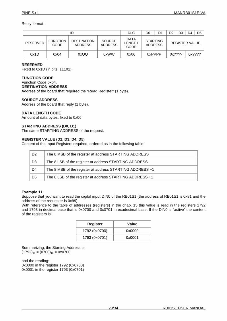
RESERVED Fixed to 0x1D (in bits: 11101). FUNCTION CODE Function Code 0x04. DESTINATION ADDRESS Address of the board that required the “Read Register” (1 byte). SOURCE ADDRESS Address of the board that reply (1 byte). DATA LENGTH CODE Amount of data bytes, fixed to 0x06. STARTING ADDRESS (D0, D1) The same STARTING ADDRESS of the request. REGISTER VALUE (D2, D3, D4, D5) Content of the Input Registers required, ordered as in the following table:
D2 The 8 MSB of the register at address STARTING ADDRESS
D3 The 8 LSB of the register at address STARTING ADDRESS
D4 The 8 MSB of the register at address STARTING ADDRESS +1
D5 The 8 LSB of the register at address STARTING ADDRESS +1
Example 11 Suppose that you want to read the digital input DIN0 of the RB01S1 (the address of RB01S1 is 0x81 and the address of the requester is 0x99). With reference to the table of addresses (registers) in the chap. 15 this value is read in the registers 1792 and 1793 in decimal base that is 0x0700 and 0x0701 in exadecimal base. If the DIN0 is “active” the content of the registers is:
Register Value
1792 (0x0700) 0x0000
1793 (0x0701) 0x0001
Summarizing, the Starting Address is: (1792)10 = (0700)16 = 0x0700 and the reading: 0x0000 in the register 1792 (0x0700) 0x0001 in the register 1793 (0x0701)

PINE S.r.l. MANRB01S1E.VA
30/34 RB01S1 USER MANUAL
Message format (request)
ID DLC D0 D1
RESERVED FUNCTION
CODE DESTINATION
ADDRESS SOURCE ADDRESS
DATA LENGTH
CODE STARTING ADDRESS
0x1D 0x04 0x81 0x99 0x02 0x0700 Reply
ID DLC D0 D1 D2 D3 D4 D5
RESERVED FUNCTION CODE
DESTINATION ADDRESS
SOURCE ADDRESS
DATA LENGTH
CODE
STARTING ADDRESS REGISTER VALUE
0x1D 0x04 0x99 0x81 0x06 0x0700 0x0000 0x0001
24. Write Registers The “Write Multiple Register” function is used for setting the value of two contiguous registers. Message format (request):
ID DLC D0 D1 D2 D3 D4 D5
RESERVED FUNCTION CODE
DESTINATION ADDRESS
SOURCE ADDRESS
DATA LENGTH
CODE
STARTING ADDRESS
REGISTER VALUE
0x1D 0x10 0xTT 0xYY 0x06 0xZZZZ 0x???? 0x????
RESERVED Fixed to 0x1D. FUNCTION CODE Function Code 0x10. DESTINATION ADDRESS Recipient’s Address ( as the “SLAVE ADDRESS in the MODBUS” , 1 byte). SOURCE ADDRESS Sender Address (1 byte). DATA LENGTH CODE Quantity of bytes of the data, fixed to 0x06. STARTING ADDRESS (D0, D1) Register Address from which you start writing. In D0 the highest part of the Register Address and in D1 the lowest. REGISTERS VALUE (D2, D3, D4, D5) Value to be written in the registers, ordered as in the following table:
D2 8 MSB of the value to write to the register at the address STARTING ADDRESS
D3 8 LSB of the value to write to the register at the address STARTING ADDRESS
D4 8 MSB of the value to write to the register at the address STARTING ADDRESS +1
D5 8 LSB of the value to write to the register at the address STARTING ADDRESS +1

PINE S.r.l. MANRB01S1E.VA
31/34 RB01S1 USER MANUAL
Reply format:
ID DLC D0 D1 D2 D3 D4 D5
RESERVED FUNCTION CODE
DESTINATION ADDRESS
SOURCE ADDRESS
DATA LENGTH
CODE
STARTING ADDRESS REGISTER VALUE
0x1D 0x10 0xYY 0xTT 0x06 0xZZZZ 0x???? 0x????
RESERVED Fixed to 0x1D. FUNCTION CODE Function Code 0x10. DESTINATION ADDRESS Address of the board that required the “Write Registers” (1 byte). SOURCE ADDRESS Address of the board that reply (1 byte). DATA LENGTH CODE Amount of bytes of the data, fixed to 0x06. STARTING ADDRESS (D0 e D1) Register Address from which you start writing. In D0 the highest part of the Register Address and in D1 the lowest. REGISTER VALUE (D2, D3, D4, D5) Value written in the registers, ordered as in the following table:
D2 8 MSB of the value writen to the register at the address STARTING ADDRESS
D3 8 LSB of the value writen to the register at the address STARTING ADDRESS
D4 8 MSB of the value writen to the register at the address STARTING ADDRESS +1
D5 8 LSB of the value writen to the register at the address STARTING ADDRESS +1 Example 12 Suppose you want to set in the analogue output AOUT0 a voltage of 6.730V (6730 mV that is 0x0000 1A4A). The address of RB01S1 is 0x95 and the address of the requester is 0xAB. With reference to the table of addresses (registers) in the chap. 15 the number 0x0000 1A4A has to be written in the registers 2304 and 2305 in decimal base, 0x0900 and 0x0901 in exadecimal base. Summarizing, the Starting Address is: (2304)10 = (0900)16 = 0x0900 and the value to write in the registers is: 0x0000 to the register 2304 (0x900) 0x1A4A to the register 2305 (0x901) Message format (request) :
ID DLC D0 D1 D2 D3 D4 D5
RESERVED FUNCTION CODE
DESTINATION ADDRESS
SOURCE ADDRESS
DATA LENGTH
CODE
STARTING ADDRESS REGISTER VALUE
0x1D 0x10 0x95 0xAB 0x06 0x9000 0x0000 0x1A4A

PINE S.r.l. MANRB01S1E.VA
32/34 RB01S1 USER MANUAL
Reply:
ID DLC D0 D1 D2 D3 D4 D5
RESERVED FUNCTION CODE
DESTINATION ADDRESS
SOURCE ADDRESS
DATA LENGTH
CODE
STARTING ADDRESS REGISTER VALUE
0x1D 0x10 0xAB 0x95 0x06 0x0900 0x0000 0x1A4A
25. Exception messages on CANBUS protocol An EXCEPTION message will be generated in the following cases: Function Code not supported: – illegal Function Code: 0x01; odd Start Addresses: – illegal data address: 0x02; (Start Address + Quantity of Registers) > 65536: – illegal data address: 0x02; attempt to write a read only registers: – slave device failure: 0x04; Data lenght not in compliance with the Function Code: – illegal data value: 0x03.
In black the Exception codes. Format of the Exception message:
ID DLC D0
RESERVED FUNCTION
CODE DESTINATION
ADDRESS SOURCE ADDRESS
DATA LENGTH
CODE
EXCEPTION CODE
0x1D 0x?? 0x?? 0x?? 0x01 0x??
RESERVED Fixed to 0x1D. FUNCTION CODE Function Code is in compliance with Exception Function Code of MODBUS RTU. DESTINATION ADDRESS Address of the requester of the function not successfully processed (1 byte). SOURCE ADDRESS Address of the board that reply (1 byte). DATA LENGTH CODE Amount of bytes of the data, fixed to 0x01. EXCEPTION CODE (D0) Exception Code is in compliance with Exception Code of MODBUS RTU. Example 13 Suppose you want to set in the analogue output AOUT0 a voltage of 6.730V (6730 mV that is 0x0000 1A4A). The address of RB01S1 is 0x95 and the address of the requester is 0xAB. With reference to the table of addresses (registers) in the chap. 15 the number 0x0000 1A4A has to be written (Function Code 0x10 ) the registers 2304 and 2305 in decimal base, 0x0900 and 0x0901 in exadecimal base. Summarizing, the Starting Address is: (2304)10 = (0900)16 = 0x0900

PINE S.r.l. MANRB01S1E.VA
33/34 RB01S1 USER MANUAL
and the value to write in the registers is: 0x0000 to the register 2304 (0x900) 0x1A4A to the register 2305 (0x901) Message format (request) with an error on Function Code:
ID DLC D0 D1 D2 D3 D4 D5
RESERVED FUNCTION CODE
DESTINATION ADDRESS
SOURCE ADDRESS
DATA LENGTH
CODE
STARTING ADDRESS REGISTER VALUE
0x1D 0x14 0x95 0xAB 0x06 0x9000 0x0000 0x1A4A
Reply:
ID DLC D0
RESERVED FUNCTION CODE
DESTINATION ADDRESS
SOURCE ADDRESS
DATA LENGTH
CODE
EXCEPTION CODE
0x1D 0x94 0xAB 0x95 0x01 0x01
FUNCTION CODE Function Code (0x14) or bit to bit (0x80). 0001 0100 or 0x14 or 1000 0000 0x80
1001 0100 0x94

PINE S.r.l. MANRB01S1E.VA
34/34 RB01S1 USER MANUAL
Per una corretta installazione ed impiego del prodotto devono essere utilizzate le informazioni tecniche contenute in questo manuale e tutte le normali precauzioni. PINE S.r.l. non è responsabile per danni o guasti provocati dal non corretto utilizzo dei prodotti. La garanzia copre al massimo il costo del prodotto stesso (cioè la sostituzione del prodotto stesso e non il rimborso) e non copre I danni causati da un uso improprio dei prodotti. Le informazioni contenute in questo manuale d’uso sono soggette a cambiamento senza preavviso. PINE S.r.l. non è responsabile di errori tecnici, di stampa o di omissioni nel presente manuale. All the normal precautions and the technical information contained in this manual must be used for a proper installation and use of the products. PINE S.r.l. is not responsible of any damage caused by improper use of the products. Warranty will not cover any damage caused by improper use of the products. The information contained herein is subject to change without notice. PINE shall not be liable for technical or editorial errors or omissions contained herein.
RB01S1 è prodotto in Italia da: PINE S.r.l. Sede legale: Via P. E. Venturini, 56 Chioggia - VE Sede operativa: Via Centro n. 49 frazione San Pietr o – 30014 Cavarzere – Venice - Italy Tel. +39 +426 357041 www.pinesrl.com [email protected]
RB01S1 is made in Italy: PINE S.r.l. Registered office: Via P. E. Venturini, 56 Chioggia - VE Head office: Via Centro n. 49 frazione San Pietro – 30014 Cavarzere – Venice - Italy Tel. +39 +426 357041 www.pinesrl.com [email protected]