general description features - future electronics
TRANSCRIPT
1
Jan. 2009 Rev. 2. 3 BCD Semiconductor Manufacturing Limited
1A LOW DROPOUT LINEAR REGULATOR AZ1117
Data Sheet
General Description
The AZ1117 is a series of low dropout three-terminalregulators with a dropout of 1.15V at 1A output cur-rent.
The AZ1117 series provides current limiting and ther-mal shutdown. Its circuit includes a trimmed bandgapreference to assure output voltage accuracy to bewithin 1% for 1.5V, 1.8V, 2.5V, 2.85V, 3.3V, 5.0V andadjustable versions or 2% for 1.2V version. Currentlimit is trimmed to ensure specified output current andcontrolled short-circuit current. On-chip thermal shut-down provides protection against any combination ofoverload and ambient temperature that would createexcessive junction temperature.
The AZ1117 has an adjustable version, that can pro-vide the output voltage from 1.25V to 12V with only 2external resistors.
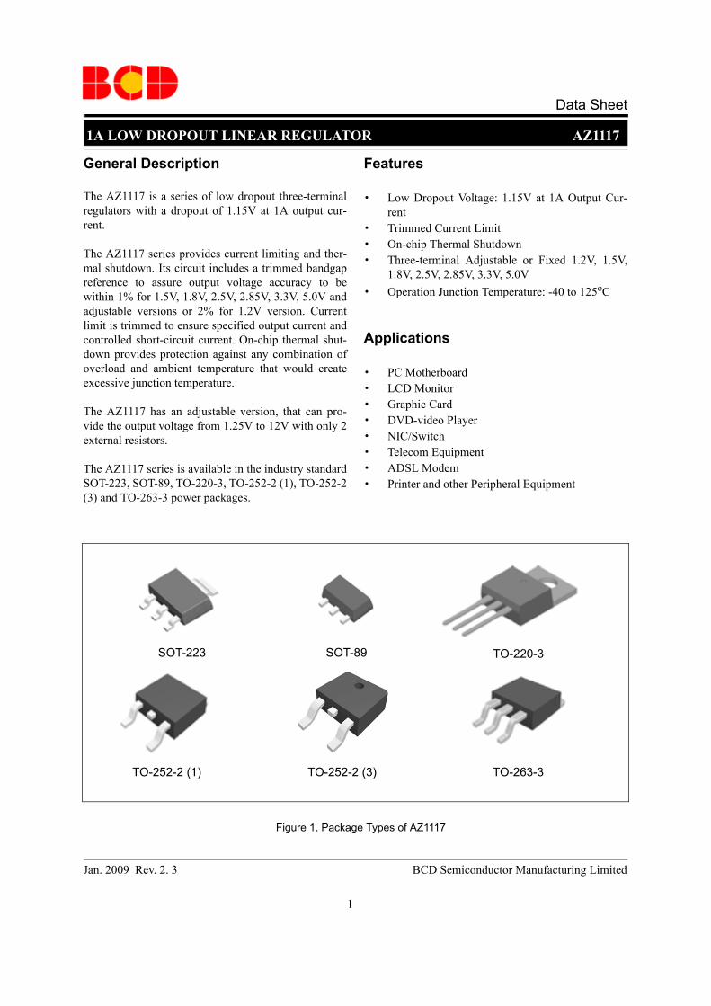
The AZ1117 series is available in the industry standardSOT-223, SOT-89, TO-220-3, TO-252-2 (1), TO-252-2(3) and TO-263-3 power packages.
Features
· Low Dropout Voltage: 1.15V at 1A Output Cur-rent
· Trimmed Current Limit· On-chip Thermal Shutdown· Three-terminal Adjustable or Fixed 1.2V, 1.5V,
1.8V, 2.5V, 2.85V, 3.3V, 5.0V· Operation Junction Temperature: -40 to 125oC
Applications
· PC Motherboard· LCD Monitor· Graphic Card · DVD-video Player · NIC/Switch · Telecom Equipment· ADSL Modem· Printer and other Peripheral Equipment
SOT-223 TO-220-3
TO-252-2 (1)
Figure 1. Package Types of AZ1117
SOT-89
TO-263-3TO-252-2 (3)
2
Jan. 2009 Rev. 2. 3 BCD Semiconductor Manufacturing Limited
1A LOW DROPOUT LINEAR REGULATOR AZ1117
Data Sheet
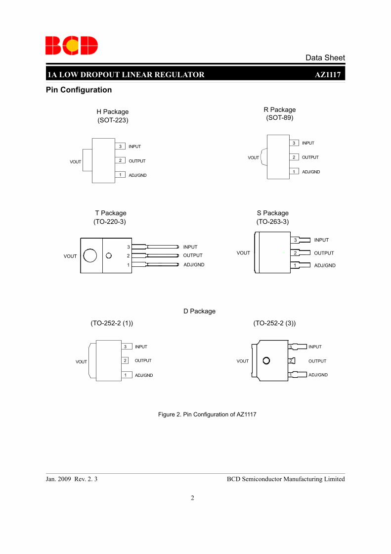
Pin Configuration
Figure 2. Pin Configuration of AZ1117
H Package(SOT-223)
T Package (TO-220-3)
(TO-252-2 (1))
R Package
S Package (TO-263-3)
D Package
(SOT-89)
VOUT
INPUT
OUTPUT
ADJ/GND1
2
3
VOUT
INPUT
OUTPUT
ADJ/GND1
2
3
1
2
3 INPUT
OUTPUT
ADJ/GND
VOUT
1
2
3 INPUT
OUTPUT
ADJ/GND
VOUT
1
2
3 INPUT
OUTPUT
ADJ/GND
VOUT
INPUT
OUTPUT
ADJ/GND
VOUT
1
2
3
(TO-252-2 (3))
3
Jan. 2009 Rev. 2. 3 BCD Semiconductor Manufacturing Limited
1A LOW DROPOUT LINEAR REGULATOR AZ1117
Data Sheet
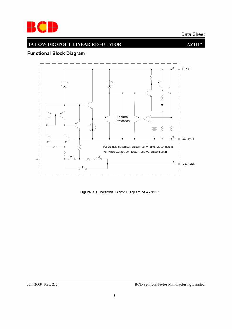
Functional Block Diagram
Figure 3. Functional Block Diagram of AZ1117
ThermalProtection +
-
For Adjustable Output, disconnect A1 and A2, connect B
INPUT
OUTPUT
ADJ/GND
A1 A2
B
For Fixed Output, connect A1 and A2, disconnect B
1
2
3
4
Jan. 2009 Rev. 2. 3 BCD Semiconductor Manufacturing Limited
1A LOW DROPOUT LINEAR REGULATOR AZ1117
Data Sheet
Circuit Type
Package
ADJ: Adjustable Output
1.5: Fixed Output 1.5V1.8: Fixed Output 1.8V2.5: Fixed Output 2.5V
3.3: Fixed Output 3.3V5.0: Fixed Output 5.0V
E1: Lead Free
AZ1117 -
TR: Tape and ReelBlank: Tube
Package Temperature RangePart Number Marking ID
Packing TypeLead Free Lead Free
SOT-223 -40 to 125oC
AZ1117H-ADJTRE1 EH11A Tape & ReelAZ1117H-1.2TRE1 EH18A Tape & ReelAZ1117H-1.5TRE1 EH12A Tape & ReelAZ1117H-1.8TRE1 EH13A Tape & ReelAZ1117H-2.5TRE1 EH14A Tape & ReelAZ1117H-2.85TRE1 EH15A Tape & ReelAZ1117H-3.3TRE1 EH16A Tape & ReelAZ1117H-5.0TRE1 EH17A Tape & Reel
SOT-89 -40 to 125oC
AZ1117R-ADJTRE1 E17A Tape & ReelAZ1117R-1.2TRE1 E17G Tape & ReelAZ1117R-1.5TRE1 E17B Tape & ReelAZ1117R-1.8TRE1 E17C Tape & ReelAZ1117R-2.5TRE1 E17D Tape & ReelAZ1117R-2.85TRE1 E17H Tape & ReelAZ1117R-3.3TRE1 E17E Tape & ReelAZ1117R-5.0TRE1 E17F Tape & Reel
TO-220-3 -40 to 125oC
AZ1117T-ADJE1 AZ1117T-ADJE1 TubeAZ1117T-1.2E1 AZ1117T-1.2E1 TubeAZ1117T-1.5E1 AZ1117T-1.5E1 TubeAZ1117T-1.8E1 AZ1117T-1.8E1 TubeAZ1117T-2.5E1 AZ1117T-2.5E1 TubeAZ1117T-2.85E1 AZ1117T-2.85E1 TubeAZ1117T-3.3E1 AZ1117T-3.3E1 TubeAZ1117T-5.0E1 AZ1117T-5.0E1 Tube
1.2: Fixed Output 1.2V
2.85: Fixed Output 2.85V
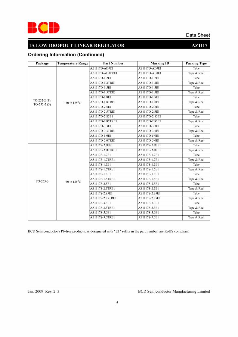
Ordering Information
R: SOT-89 D: TO-252-2 (1)/(3)H: SOT-223
T: TO-220-3 S: TO-263-3
5
Jan. 2009 Rev. 2. 3 BCD Semiconductor Manufacturing Limited
1A LOW DROPOUT LINEAR REGULATOR AZ1117
Data Sheet
Package Temperature Range Part Number Marking ID Packing Type
TO-252-2 (1)/TO-252-2 (3) -40 to 125oC
AZ1117D-ADJE1 AZ1117D-ADJE1 TubeAZ1117D-ADJTRE1 AZ1117D-ADJE1 Tape & ReelAZ1117D-1.2E1 AZ1117D-1.2E1 TubeAZ1117D-1.2TRE1 AZ1117D-1.2E1 Tape & ReelAZ1117D-1.5E1 AZ1117D-1.5E1 TubeAZ1117D-1.5TRE1 AZ1117D-1.5E1 Tape & ReelAZ1117D-1.8E1 AZ1117D-1.8E1 TubeAZ1117D-1.8TRE1 AZ1117D-1.8E1 Tape & ReelAZ1117D-2.5E1 AZ1117D-2.5E1 TubeAZ1117D-2.5TRE1 AZ1117D-2.5E1 Tape & ReelAZ1117D-2.85E1 AZ1117D-2.85E1 TubeAZ1117D-2.85TRE1 AZ1117D-2.85E1 Tape & ReelAZ1117D-3.3E1 AZ1117D-3.3E1 TubeAZ1117D-3.3TRE1 AZ1117D-3.3E1 Tape & ReelAZ1117D-5.0E1 AZ1117D-5.0E1 TubeAZ1117D-5.0TRE1 AZ1117D-5.0E1 Tape & Reel
TO-263-3 -40 to 125oC
AZ1117S-ADJE1 AZ1117S-ADJE1 TubeAZ1117S-ADJTRE1 AZ1117S-ADJE1 Tape & ReelAZ1117S-1.2E1 AZ1117S-1.2E1 TubeAZ1117S-1.2TRE1 AZ1117S-1.2E1 Tape & ReelAZ1117S-1.5E1 AZ1117S-1.5E1 TubeAZ1117S-1.5TRE1 AZ1117S-1.5E1 Tape & ReelAZ1117S-1.8E1 AZ1117S-1.8E1 TubeAZ1117S-1.8TRE1 AZ1117S-1.8E1 Tape & ReelAZ1117S-2.5E1 AZ1117S-2.5E1 TubeAZ1117S-2.5TRE1 AZ1117S-2.5E1 Tape & ReelAZ1117S-2.85E1 AZ1117S-2.85E1 TubeAZ1117S-2.85TRE1 AZ1117S-2.85E1 Tape & ReelAZ1117S-3.3E1 AZ1117S-3.3E1 TubeAZ1117S-3.3TRE1 AZ1117S-3.3E1 Tape & ReelAZ1117S-5.0E1 AZ1117S-5.0E1 TubeAZ1117S-5.0TRE1 AZ1117S-5.0E1 Tape & Reel
Ordering Information (Continued)
BCD Semiconductor's Pb-free products, as designated with "E1" suffix in the part number, are RoHS compliant.
6
Jan. 2009 Rev. 2. 3 BCD Semiconductor Manufacturing Limited
1A LOW DROPOUT LINEAR REGULATOR AZ1117
Data Sheet
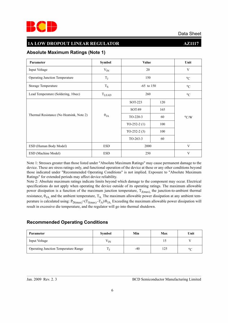
Note 1: Stresses greater than those listed under "Absolute Maximum Ratings" may cause permanent damage to thedevice. These are stress ratings only, and functional operation of the device at these or any other conditions beyondthose indicated under "Recommended Operating Conditions" is not implied. Exposure to "Absolute MaximumRatings" for extended periods may affect device reliability. Note 2: Absolute maximum ratings indicate limits beyond which damage to the component may occur. Electricalspecifications do not apply when operating the device outside of its operating ratings. The maximum allowablepower dissipation is a function of the maximum junction temperature, TJ(max), the junction-to-ambient thermalresistance, θJA, and the ambient temperature, TA. The maximum allowable power dissipation at any ambient tem-perature is calculated using: PD(max)=(TJ(max) -TA)/θJA. Exceeding the maximum allowable power dissipation willresult in excessive die temperature, and the regulator will go into thermal shutdown.
Recommended Operating Conditions
Parameter Symbol Value Unit
Input Voltage VIN 20 V
Operating Junction Temperature TJ 150 oC
Storage Temperature TS -65 to 150 oC
Lead Temperature (Soldering, 10sec) TLEAD 260 oC
Thermal Resistance (No Heatsink, Note 2) θJA
SOT-223 120
oC/W
SOT-89 165
TO-220-3 60
TO-252-2 (1) 100
TO-252-2 (3) 100
TO-263-3 60
ESD (Human Body Model) ESD 2000 V
ESD (Machine Model) ESD 250 V
Parameter Symbol Min Max Unit
Input Voltage VIN 15 V
Operating Junction Temperature Range TJ -40 125 oC
Absolute Maximum Ratings (Note 1)

7
Jan. 2009 Rev. 2. 3 BCD Semiconductor Manufacturing Limited
1A LOW DROPOUT LINEAR REGULATOR AZ1117
Data Sheet
Parameter Symbol Conditions Min Typ Max Unit
Reference Voltage VREF IOUT = 10mΑ, VIN-VOUT = 2V10mA≤ IOUT ≤ 1Α, 1.4V≤ VIN-VOUT ≤ 8V, P≤ Maximum Power Dissipation
1.238 1.225
1.250 1.250
1.2621.270
V
Line Regulation ∆VOUT IOUT=10mA, 1.5V≤VIN-VOUT≤10V 0.035 0.2 %
Load Regulation ∆VOUT VIN-VOUT=2V, 10mA≤ IOUT≤1Α 0.2 0.4 %
Dropout Voltage VDROP
∆VREF=1%, IOUT=0.1Α 1.00 1.1 V
∆VREF =1%, IOUT=0.5Α 1.08 1.18 V
∆VREF=1%, IOUT=1.0Α 1.15 1.25 V
Current Limit ILIMIT VIN-VOUT=2V 1.25 1.35 A
Adjust Pin Current IADJ 60 120 µA
Adjust Pin CurrentChange
∆IADJ
1.4V≤VIN-VOUT≤10V, 10mA≤IOUT ≤1A 0.2 5 µA
Minimum Load Current(ADJ)
ILOAD(MIN) 1.5V≤VIN-VOUT≤10V (ADJ only) 1.7 5 mA
Quiescent Current IQ VIN=VOUT +1.25V 5 10 mA
Ripple Rejection PSRR f=120Hz, COUT=22µF Tantalum, VIN-VOUT=3V, IOUT =1A
60 75 dB
Temperature Stability 0.5 %
Long-term Stability TA=125oC, 1000hrs 0.3 %
RMS Output Noise (% of VOUT)
TA=25oC, 10Hz≤f≤10kHz 0.003 %
Thermal Shutdown Junction Temperature 150 oC
Thermal Shutdown Hysteresis 25 oC
Thermal Resistance θJC
SOT-223 25
oC/W
SOT-89 30
TO-220-3 10
TO-252-2 (1) 17
TO-252-2 (3) 17
TO-263-3 10
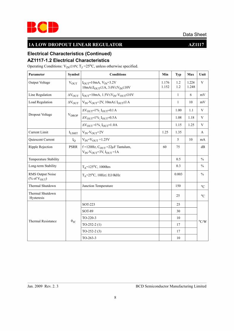
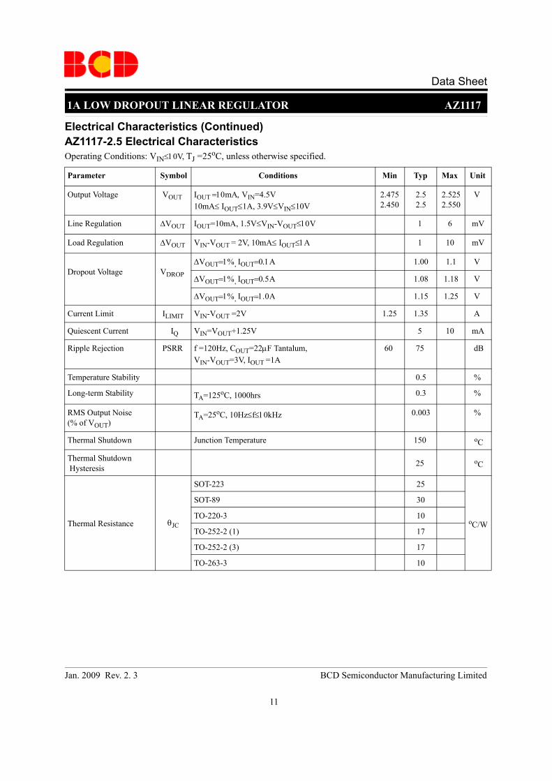
Operating Conditions: VIN≤10V, TJ =25oC, unless otherwise specified.
Electrical CharacteristicsAZ1117-ADJ Electrical Characteristics
8
Jan. 2009 Rev. 2. 3 BCD Semiconductor Manufacturing Limited
1A LOW DROPOUT LINEAR REGULATOR AZ1117
Data Sheet
Parameter Symbol Conditions Min Typ Max Unit
Output Voltage VOUT IOUT=10mΑ, VIN=3.2V10mA≤IOUT≤1A, 3.0V≤VIN≤10V
1.176 1.152
1.21.2
1.224 1.248
V
Line Regulation ∆VOUT IOUT=10mA, 1.5V≤VIN-VOUT≤10V 1 6 mV
Load Regulation ∆VOUT VIN-VOUT=2V, 10mA≤ IOUT≤1Α 1 10 mV
Dropout Voltage VDROP
∆VOUT=1%, IOUT=0.1Α 1.00 1.1 V
∆VOUT=1%, IOUT=0.5Α 1.08 1.18 V
∆VOUT =1%, IOUT=1.0Α 1.15 1.25 V
Current Limit ILIMIT VIN-VOUT=2V 1.25 1.35 A
Quiescent Current IQ VIN=VOUT +1.25V 5 10 mA
Ripple Rejection PSRR f =120Hz, COUT =22µF Tantalum, VIN-VOUT=3V, IOUT =1A
60 75 dB
Temperature Stability 0.5 %
Long-term Stability TA=125oC, 1000hrs 0.3 %
RMS Output Noise (% of VOUT)
TA=25oC, 10Hz≤ f≤10kHz 0.003 %
Thermal Shutdown Junction Temperature 150 oC
Thermal Shutdown Hysteresis 25 oC
Thermal Resistance θJC
SOT-223 25
oC/W
SOT-89 30
TO-220-3 10
TO-252-2 (1) 17
TO-252-2 (3) 17
TO-263-3 10
Operating Conditions: VIN≤10V, TJ =25oC, unless otherwise specified.AZ1117-1.2 Electrical Characteristics Electrical Characteristics (Continued)

9
Jan. 2009 Rev. 2. 3 BCD Semiconductor Manufacturing Limited
1A LOW DROPOUT LINEAR REGULATOR AZ1117
Data Sheet
Parameter Symbol Conditions Min Typ Max Unit
Output Voltage VOUT IOUT=10mΑ, VIN=3.5V10mA≤IOUT≤1A, 3.0V≤VIN≤10V
1.485 1.470
1.5 1.5
1.515 1.530
V
Line Regulation ∆VOUT IOUT=10mA, 1.5V≤ VIN-VOUT ≤10V 1 6 mV
Load Regulation ∆VOUT VIN-VOUT =2V, 10mA≤ IOUT≤1Α 1 10 mV
Dropout Voltage VDROP
∆VOUT=1%, IOUT=0.1Α 1.00 1.1 V
∆VOUT=1%, IOUT=0.5Α 1.08 1.18 V
∆VOUT=1%, IOUT=1.0Α 1.15 1.25 V
Current Limit ILIMIT VIN-VOUT =2V 1.25 1.35 A
Quiescent Current IQ VIN=VOUT+1.25V 5 10 mA
Ripple Rejection PSRR f=120Hz, COUT =22µF Tantalum, VIN-VOUT =3V, IOUT=1A
60 75 dB
Temperature Stability 0.5 %
Long-term Stability TA=125oC, 1000hrs 0.3 %
RMS Output Noise (% of VOUT)
TA=25oC, 10Hz≤f≤10kHz 0.003 %
Thermal Shutdown Junction Temperature 150 oC
Thermal Shutdown Hysteresis 25 oC
Thermal Resistance θJC
SOT-223 25
oC/W
SOT-89 30
TO-220-3 10
TO-252-2 (1) 17
TO-252-2 (3) 17
TO-263-3 10
Operating Conditions: VIN≤10V, TJ =25oC, unless otherwise specified.AZ1117-1.5 Electrical Characteristics Electrical Characteristics (Continued)

10
Jan. 2009 Rev. 2. 3 BCD Semiconductor Manufacturing Limited
1A LOW DROPOUT LINEAR REGULATOR AZ1117
Data Sheet
Parameter Symbol Conditions Min Typ Max Unit
Output Voltage VOUT IOUT=10mΑ, VIN=3.8V10mA≤ IOUT≤1A, 3.2V≤VIN≤10V
1.782 1.746
1.8 1.8
1.818 1.854
V
Line Regulation ∆VOUT IOUT=10mA, 1.5V≤VIN-VOUT≤10V 1 6 mV
Load Regulation ∆VOUT VIN-VOUT=2V, 10mA≤ IOUT≤1Α 1 10 mV
Dropout Voltage VDROP
∆VOUT=1%, IOUT=0.1Α 1.00 1.1 V
∆VOUT=1%, IOUT=0.5Α 1.08 1.18 V
∆VOUT=1%, IOUT=1.0Α 1.15 1.25 V
Current Limit ILIMIT VIN-VOUT=2V 1.25 1.35 A
Quiescent Current IQ VIN=VOUT +1.25V 5 10 mA
Ripple Rejection PSRR f =120Hz, COUT =22µF Tantalum, VIN-VOUT=3V, IOUT =1A
60 75 dB
Temperature Stability 0.5 %
Long-term Stability TA=125oC, 1000hrs 0.3 %
RMS Output Noise (% of VOUT)
TA=25oC, 10Hz ≤ f ≤ 10kHz 0.003 %
Thermal Shutdown Junction Temperature 150 oC
Thermal Shutdown Hysteresis 25 oC
Thermal Resistance θJC
SOT-223 25
oC/W
SOT-89 30
TO-220-3 10
TO-252-2 (1) 17
TO-252-2 (3) 17
TO-263-3 10
Operating Conditions: VIN≤10V, TJ =25oC, unless otherwise specified.AZ1117-1.8 Electrical Characteristics Electrical Characteristics (Continued)
11
Jan. 2009 Rev. 2. 3 BCD Semiconductor Manufacturing Limited
1A LOW DROPOUT LINEAR REGULATOR AZ1117
Data Sheet
Parameter Symbol Conditions Min Typ Max Unit
Output Voltage VOUT IOUT =10mΑ, VIN=4.5V10mA≤ IOUT≤1A, 3.9V≤VIN≤10V
2.475 2.450
2.5 2.5
2.525 2.550
V
Line Regulation ∆VOUT IOUT=10mA, 1.5V≤VIN-VOUT≤10V 1 6 mV
Load Regulation ∆VOUT VIN-VOUT = 2V, 10mA≤ IOUT≤1Α 1 10 mV
Dropout Voltage VDROP
∆VOUT=1%, IOUT=0.1Α 1.00 1.1 V
∆VOUT=1%, IOUT=0.5Α 1.08 1.18 V
∆VOUT=1%, IOUT=1.0Α 1.15 1.25 V
Current Limit ILIMIT VIN-VOUT =2V 1.25 1.35 A
Quiescent Current IQ VIN=VOUT+1.25V 5 10 mA
Ripple Rejection PSRR f =120Hz, COUT=22µF Tantalum, VIN-VOUT=3V, IOUT =1A
60 75 dB
Temperature Stability 0.5 %
Long-term Stability TA=125oC, 1000hrs 0.3 %
RMS Output Noise (% of VOUT)
TA=25oC, 10Hz≤f≤10kHz 0.003 %
Thermal Shutdown Junction Temperature 150 oC
Thermal Shutdown Hysteresis 25 oC
Thermal Resistance θJC
SOT-223 25
oC/W
SOT-89 30
TO-220-3 10
TO-252-2 (1) 17
TO-252-2 (3) 17
TO-263-3 10
Operating Conditions: VIN≤10V, TJ =25oC, unless otherwise specified.AZ1117-2.5 Electrical Characteristics Electrical Characteristics (Continued)

12
Jan. 2009 Rev. 2. 3 BCD Semiconductor Manufacturing Limited
1A LOW DROPOUT LINEAR REGULATOR AZ1117
Data Sheet
Parameter Symbol Conditions Min Typ Max Unit
Output Voltage VOUT IOUT=10mA, VIN=4.85V10mA≤IOUT≤ 1A, 4.25V≤VIN≤10V
2.822 2.793
2.852.85
2.8782.907
V
Line Regulation ∆VOUT IOUT=10mA, 1.5V≤VIN-VOUT≤10V 1 6 mV
Load Regulation ∆VOUT VIN-VOUT=2V, 10mA≤ IOUT≤1Α 1 10 mV
Dropout Voltage VDROP
∆VREF=1%, IOUT=0.1A 1.00 1.1 V
∆VREF=1%, IOUT=0.5A 1.08 1.18 V
∆VREF=1%, IOUT=1.0A 1.15 1.25 V
Current Limit ILIMIT VIN-VOUT=2V 1.25 1.35 A
Quiescent Current IQ VIN=VOUT+1.25V 5 10 mA
Ripple Rejection PSRR f =120Hz, COUT=22µF Tantalum, VIN-VOUT=3V, IOUT =1A
60 75 dB
Temperature Stability 0.5 %
Long-term Stability TA=125oC, 1000hrs 0.3 %
RMS Output Noise (% of VOUT)
TA=25oC, 10Hz≤f≤10kHz 0.003 %
Thermal Shutdown Junction Temperature 150 oC
Thermal Shutdown Hysteresis 25 oC
Thermal Resistance θJC
SOT-223 25
oC/W
SOT-89 30
TO-220-3 10
TO-252-2 (1) 17
TO-252-2 (3) 17
TO-263-3 10
AZ1117-2.85 Electrical Characteristics
Operating Conditions: VIN≤10V, TJ =25oC, unless otherwise specified.
Electrical Characteristics (Continued)

13
Jan. 2009 Rev. 2. 3 BCD Semiconductor Manufacturing Limited
1A LOW DROPOUT LINEAR REGULATOR AZ1117
Data Sheet
Parameter Symbol Conditions Min Typ Max Unit
Output Voltage VOUT IOUT =10mΑ, VIN=5.0V10mA≤ IOUT≤1A, 4.75V≤VIN≤10V
3.267 3.235
3.3 3.3
3 .3333.365
V
Line Regulation ∆VOUT IOUT=10mA, 1.5V≤VIN-VOUT≤10V 1 6 mV
Load Regulation ∆VOUT VIN-VOUT=2V, 10mA≤IOUT ≤1Α 1 10 mV
Dropout Voltage VDROP
∆VOUT=1%, IOUT=0.1Α 1.00 1.1 V
∆VOUT=1%, IOUT=0.5Α 1.08 1.18 V
∆VOUT=1%, IOUT=1.0Α 1.15 1.25 V
Current Limit ILIMIT VIN-VOUT=2V 1.25 1.35 A
Quiescent Current IQ VIN=VOUT +1.25V 5 10 mA
Ripple Rejection PSRR f=120Hz, COUT=22µF Tantalum, VIN-VOUT=3V, IOUT =1A
60 75 dB
Temperature Stability 0.5 %
Long-term Stability TA=125oC, 1000hrs 0.3 %
RMS Output Noise (% of VOUT)
TA=25oC, 10Hz≤f≤10kHz 0.003 %
Thermal Shutdown Junction Temperature 150 oC
Thermal Shutdown Hysteresis 25 oC
Thermal Resistance θJC
SOT-223 25
oC/W
SOT-89 30
TO-220-3 10
TO-252-2 (1) 17
TO-252-2 (3) 17
TO-263-3 10
Operating Conditions: VIN≤10V, TJ =25oC, unless otherwise specified.AZ1117-3.3 Electrical Characteristics Electrical Characteristics (Continued)
14
Jan. 2009 Rev. 2. 3 BCD Semiconductor Manufacturing Limited
1A LOW DROPOUT LINEAR REGULATOR AZ1117
Data Sheet
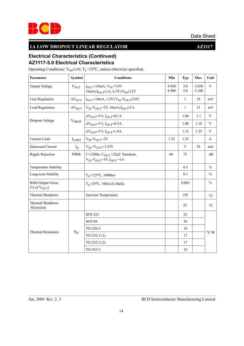
Parameter Symbol Conditions Min Typ Max Unit
Output Voltage VOUT IOUT =10mΑ, VIN=7.0V10mA≤IOUT≤1A, 6.5V≤VIN≤12V
4.950 4.900
5.0 5.0
5.050 5.100
V
Line Regulation ∆VOUT IOUT=10mA, 1.5V≤VIN-VOUT≤10V 1 10 mV
Load Regulation ∆VOUT VIN-VOUT=2V, 10mA≤IOUT≤1Α 1 15 mV
Dropout Voltage VDROP
∆VOUT=1%, IOUT=0.1Α 1.00 1.1 V
∆VOUT=1%, IOUT=0.5Α 1.08 1.18 V
∆VOUT=1%, IOUT=1.0Α 1.15 1.25 V
Current Limit ILIMIT VIN-VOUT=2V 1.25 1.35 A
Quiescent Current IQ VIN=VOUT+1.25V 5 10 mA
Ripple Rejection PSRR f =120Hz, COUT =22µF Tantalum, VIN-VOUT=3V, IOUT =1A
60 75 dB
Temperature Stability 0.5 %
Long-term Stability TA=125oC, 1000hrs 0.3 %
RMS Output Noise (% of VOUT)
TA=25oC, 10Hz≤f≤10kHz 0.003 %
Thermal Shutdown Junction Temperature 150 oC
Thermal Shutdown Hysteresis 25 oC
Thermal Resistance θJC
SOT-223 25
oC/W
SOT-89 30
TO-220-3 10
TO-252-2 (1) 17
TO-252-2 (3) 17
TO-263-3 10
Operating Conditions: VIN≤10V, TJ =25oC, unless otherwise specified.AZ1117-5.0 Electrical Characteristics Electrical Characteristics (Continued)

15
Jan. 2009 Rev. 2. 3 BCD Semiconductor Manufacturing Limited
1A LOW DROPOUT LINEAR REGULATOR AZ1117
Data Sheet
Typical Performance Characteristics
Figure 6. Load Regulation vs. Junction Temperature Figure 7. Reference Voltage vs. Junction Temperature
-50 -25 0 25 50 75 100 1251.230
1.235
1.240
1.245
1.250
1.255
1.260
1.265
1.270
1.275
1.280
Ref
eren
ce V
olta
ge (V
)
Junction Temperature (oC)-50 -25 0 25 50 75 100 125
-0.2
-0.1
0.0
0.1
0.2
Out
put V
olta
ge D
evia
tion
(%)
Junction Temperature (oC)
AZ1117-ADJ
Figure 4. Dropout Voltage vs. Output Current
0.2 0.4 0.6 0.8 1.00.5
0.6
0.7
0.8
0.9
1.0
1.1
1.2
TA=125oC
TA=25oC
TA=0oC
Dro
pout
Vol
tage
(V)
Output Current (A)
-40 -20 0 20 40 60 80 100 1200.80
0.85
0.90
0.95
1.00
1.05
1.10
1.15
Dro
pout
Vol
tage
(V)
Junction Temperature (oC)
IOUT
=0.1A IOUT=0.5A IOUT=1A
∆VREF=1%
Figure 5. Dropout Voltage vs. Junction Temperature
16
Jan. 2009 Rev. 2. 3 BCD Semiconductor Manufacturing Limited
1A LOW DROPOUT LINEAR REGULATOR AZ1117
Data Sheet
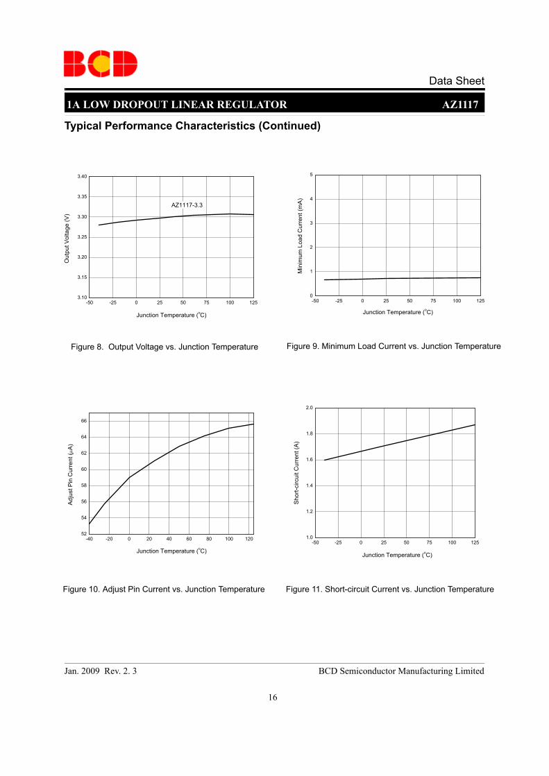
Figure 9. Minimum Load Current vs. Junction Temperature
Figure 11. Short-circuit Current vs. Junction Temperature
Typical Performance Characteristics (Continued)
Figure 10. Adjust Pin Current vs. Junction Temperature
-50 -25 0 25 50 75 100 1251.0
1.2
1.4
1.6
1.8
2.0
Shor
t-circ
uit C
urre
nt (A
)
Junction Temperature (oC)
-50 -25 0 25 50 75 100 1250
1
2
3
4
5
Min
imum
Loa
d C
urre
nt (m
A)
Junction Temperature (oC)
-40 -20 0 20 40 60 80 100 12052
54
56
58
60
62
64
66
Adju
st P
in C
urre
nt (µ
A)
Junction Temperature (oC)
Figure 8. Output Voltage vs. Junction Temperature
-50 -25 0 25 50 75 100 1253.10
3.15
3.20
3.25
3.30
3.35
3.40
AZ1117-3.3
Out
put V
olta
ge (V
)
Junction Temperature (oC)
17
Jan. 2009 Rev. 2. 3 BCD Semiconductor Manufacturing Limited
1A LOW DROPOUT LINEAR REGULATOR AZ1117
Data Sheet
Typical Performance Characteristics (Continued)
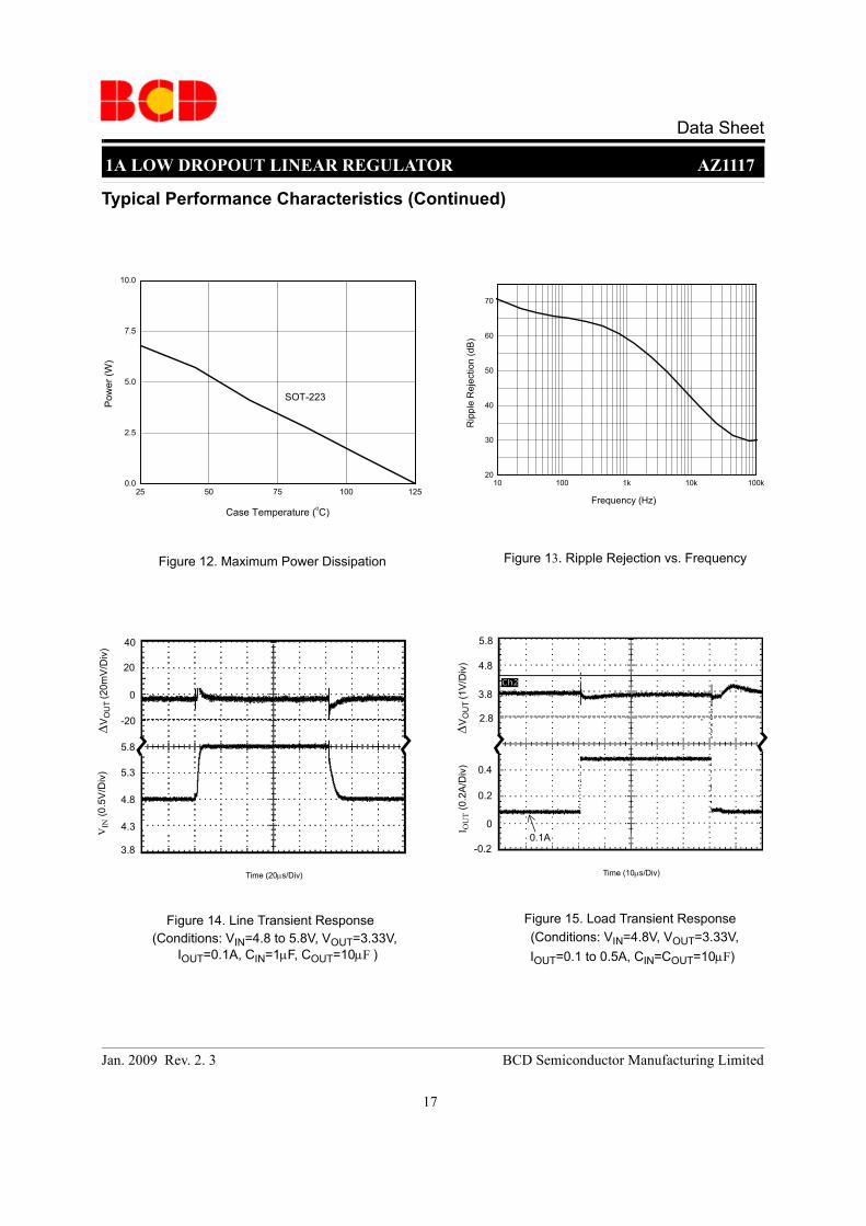
Figure 14. Line Transient Response Figure 15. Load Transient Response(Conditions: VIN=4.8 to 5.8V, VOUT=3.33V,
IOUT=0.1A, CIN=1µF, COUT=10µF )
Time (20µs/Div)
-20
0
20
40
4.8
3.8
4.3
5.3
VIN
(0.5
V/D
iv)
∆V O
UT
(20m
V/D
iv)
Time (10µs/Div)
(Conditions: VIN=4.8V, VOUT=3.33V, IOUT=0.1 to 0.5A, CIN=COUT=10µF)
2.8
3.8
4.8
5.8
0.4
-0.2
0
0.2
I OU
T (0
.2A
/Div
)
∆V
OU
T (1
V/D
iv)
5.8
0.1A
Figure 12. Maximum Power Dissipation
25 50 75 100 1250.0
2.5
5.0
7.5
10.0
SOT-223
Pow
er (W
)
Case Temperature (oC)
10 100 1k 10k 100k20
30
40
50
60
70
Rip
ple
Rej
ectio
n (d
B)
Frequency (Hz)
Figure 13. Ripple Rejection vs. Frequency
18
Jan. 2009 Rev. 2. 3 BCD Semiconductor Manufacturing Limited
1A LOW DROPOUT LINEAR REGULATOR AZ1117
Data Sheet
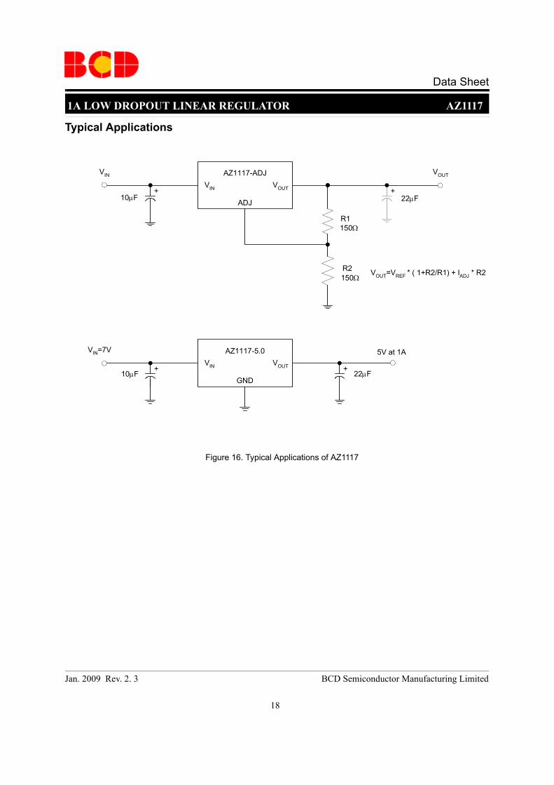
Typical Applications
Figure 16. Typical Applications of AZ1117
AZ1117-ADJVIN VOUT
ADJ
VIN
10µF
R1
R2
22µF
VOUT
+ +
+ +
VIN=7V AZ1117-5.0VIN VOUT
GND 10µF 22µF
5V at 1A
VOUT=VREF * ( 1+R2/R1) + IADJ * R2
150Ω
150Ω
19
Jan. 2009 Rev. 2. 3 BCD Semiconductor Manufacturing Limited
1A LOW DROPOUT LINEAR REGULATOR AZ1117
Data Sheet
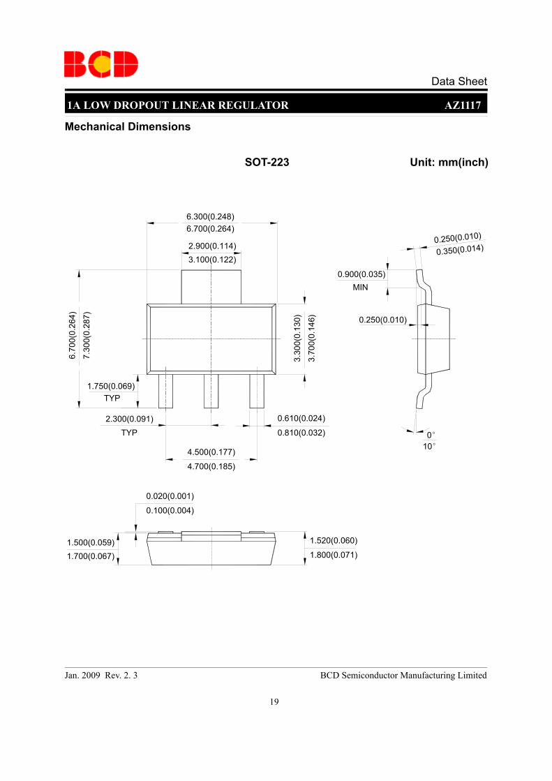
Mechanical Dimensions
SOT-223 Unit: mm(inch)
3.30
0(0.
130)
3.70
0(0.
146)
6.70
0(0.
264)
7.30
0(0.
287)
2.900(0.114)3.100(0.122)
0.610(0.024)
0.810(0.032)2.300(0.091)
TYP
6.300(0.248)6.700(0.264)
1.750(0.069)TYP
4.500(0.177)
4.700(0.185)
0.020(0.001)
0.100(0.004)
1.520(0.060)
1.800(0.071)1.500(0.059)1.700(0.067)
0.250(0.010)
0.350(0.014)
0.250(0.010)
0° 10°
0.900(0.035)MIN
20
Jan. 2009 Rev. 2. 3 BCD Semiconductor Manufacturing Limited
1A LOW DROPOUT LINEAR REGULATOR AZ1117
Data Sheet
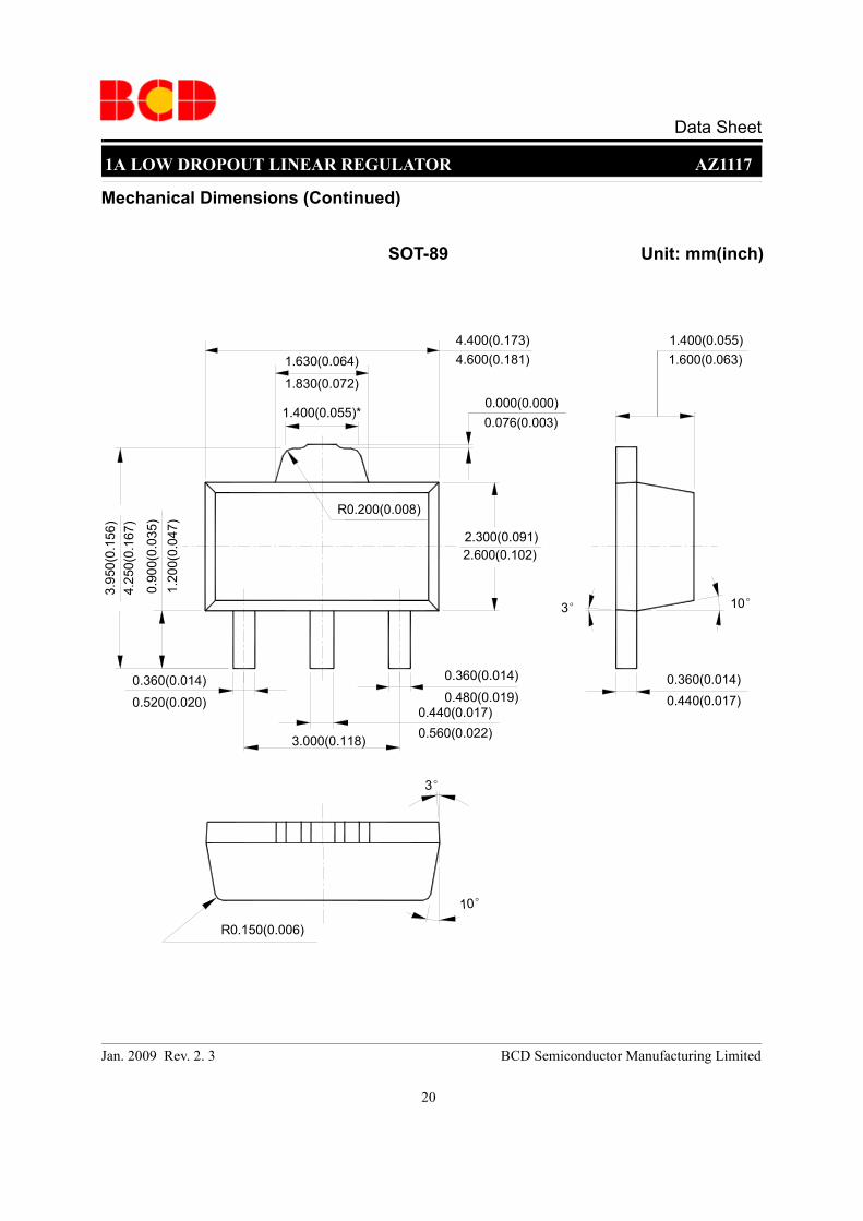
Mechanical Dimensions (Continued)
SOT-89 Unit: mm(inch)
1.400(0.055)*
1.630(0.064)4.400(0.173)
0.360(0.014)
0.440(0.017)
3.000(0.118)
0.90
0(0.
0 35)
2.300(0.091)
3.95
0(0.
1 56)
1.400(0.055)
0.360(0.014)
10°
3°
10°
R0.200(0.008)
R0.150(0.006)
0.000(0.000)
3°
1.600(0.063)
0.440(0.017)
0.560(0.022)
2.600(0.102)
0.520(0.020)
4.600(0.181)
1.830(0.072)
1.20
0 (0.
047)
4.25
0(0.
167)
0.076(0.003)
0.360(0.014)
0.480(0.019)
21
Jan. 2009 Rev. 2. 3 BCD Semiconductor Manufacturing Limited
1A LOW DROPOUT LINEAR REGULATOR AZ1117
Data Sheet
Mechanical Dimensions (Continued)
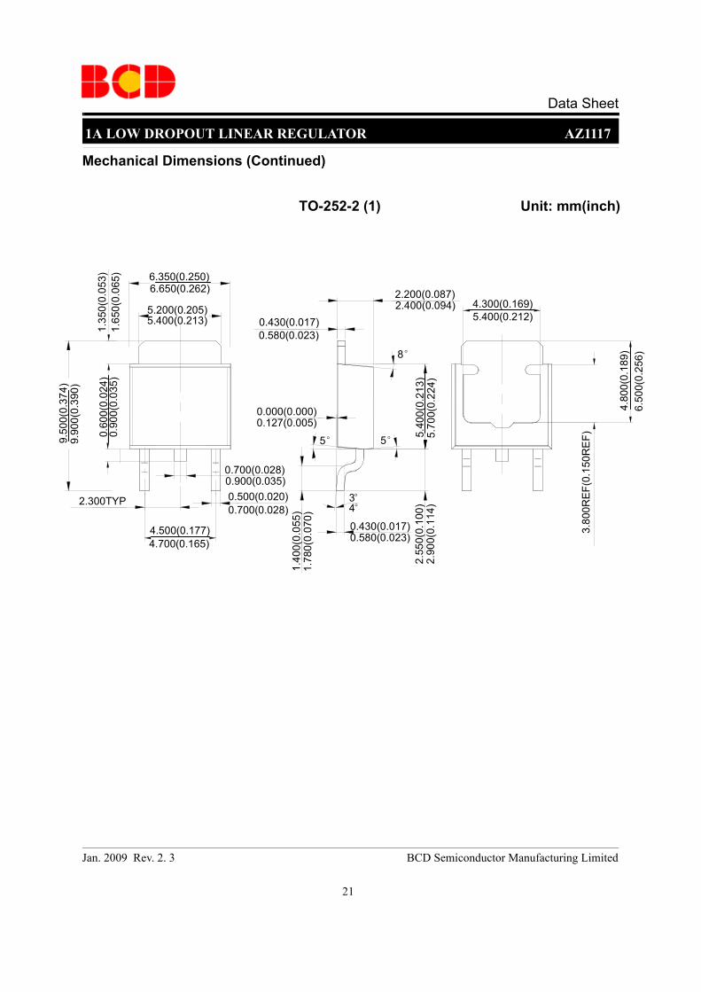
Unit: mm(inch)TO-252-2 (1)
1.35
0(0.
053)
1.65
0(0.
065)
0.60
0(0.
024)
0.90
0(0.
035)
4.500(0.177)4.700(0.165)
3°4°
3.80
0RE
F(0.
150R
EF)
4.80
0(0.
189)
6.50
0(0.
256)
4.300(0.169)5.400(0.212)
1.40
0(0.
055)
1.78
0(0.
070)
0.000(0.000)0.127(0.005)
0.430(0.017)0.580(0.023)
2.300TYP
9.50
0(0.
374)
9.90
0(0.
390)
0.700(0.028)0.900(0.035)0.500(0.020)0.700(0.028)
5.200(0.205)5.400(0.213)
6.350(0.250)6.650(0.262)
2.55
0(0.
100)
2.90
0(0.
114)
5.40
0(0.
213)
5.70
0(0.
224)
2.200(0.087)2.400(0.094)
5° 5°
8°
0.430(0.017)0.580(0.023)
22
Jan. 2009 Rev. 2. 3 BCD Semiconductor Manufacturing Limited
1A LOW DROPOUT LINEAR REGULATOR AZ1117
Data Sheet
Mechanical Dimensions (Continued)
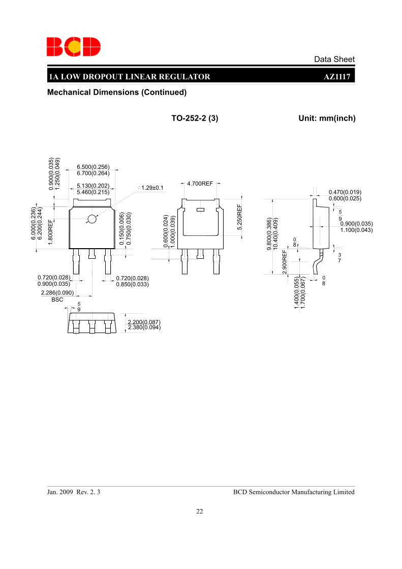
Unit: mm(inch)TO-252-2 (3)
1.29±0.1
2.90
0RE
F
1.40
0(0.
055)
1.70
0(0.
067)
0.470(0.019)0.600(0.025)
59
089.
800(
0.38
6)10
.40(
0.40
9)
2.200(0.087)2.380(0.094)
0.900(0.035)1.100(0.043)
4.700REF
5.25
0RE
F
6.500(0.256)6.700(0.264)
5.130(0.202)5.460(0.215)
0.15
0(0.
006)
0.75
0(0.
030)
6.00
0(0.
236)
6.20
0(0.
244)
0.720(0.028)0.850(0.033)
2.286(0.090)BSC
0.720(0.028)0.900(0.035)
0.90
0(0.
035)
1.25
0(0.
049)
1.80
0RE
F
80
0.60
0(0.
024)
1.00
0(0.
039)
73
95
23
Jan. 2009 Rev. 2. 3 BCD Semiconductor Manufacturing Limited
1A LOW DROPOUT LINEAR REGULATOR AZ1117
Data Sheet
Mechanical Dimensions (Continued)
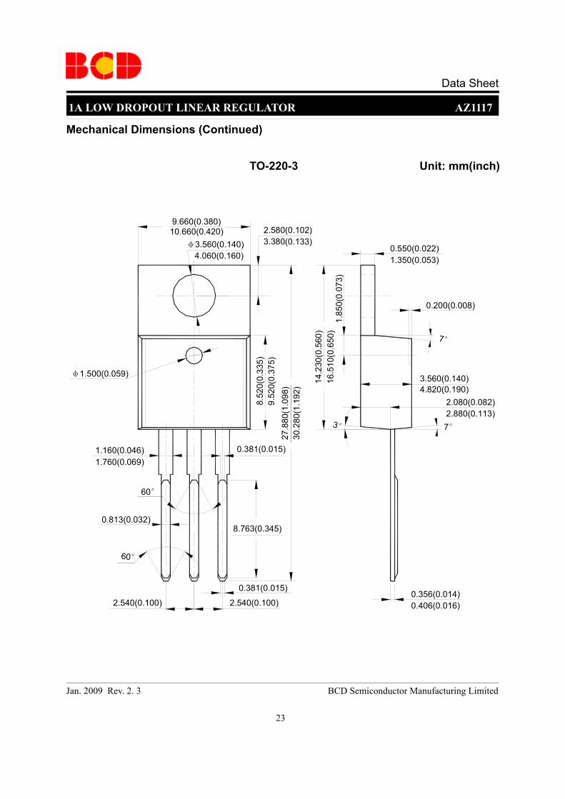
TO-220-3 Unit: mm(inch)
φ3.560(0.140)
14.2
30( 0
.560
)
1.160(0.046)
0.813(0.032)8.763(0.345)
2.540(0.100)0.356(0.014)
2.080(0.082)
3° 7°
3.560(0.140)
7°
9.660(0.380)
0.550(0.022)
60°
0.381(0.015)
2.580(0.102)
60°
8.52
0(0.
335)
φ1.500(0.059)
0.200(0.008)
1.85
0(0.
073)
2.540(0.100)
0.381(0.015)
0.406(0.016)
3.380(0.133)10.660(0.420)
4.060(0.160) 1.350(0.053)
27.8
80(1
.098
)30
.280
(1.1
92)
9.52
0 (0.
375)
16.5
10(0
. 650
)
4.820(0.190)
2.880(0.113)
1.760(0.069)
24
Jan. 2009 Rev. 2. 3 BCD Semiconductor Manufacturing Limited
1A LOW DROPOUT LINEAR REGULATOR AZ1117
Data Sheet
Mechanical Dimensions (Continued)
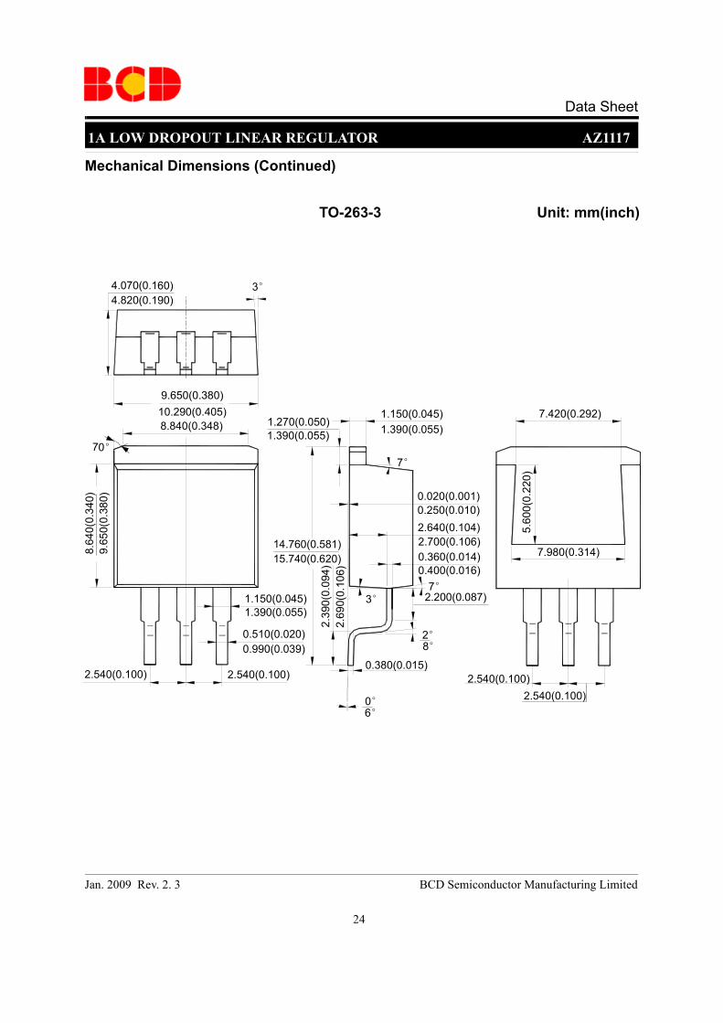
TO-263-3 Unit: mm(inch)
7°
3°7°
8.64
0(0.
3 40)
9.65
0(0.
380 )
0.990(0.039)0.510(0.020)
2.540(0.100)
1.150(0.045)
9.650(0.380)
3°
14.760(0.581)
8.840(0.348)
2.640(0.104)
0.020(0.001)
8°2°
0°6°
0.380(0.015)
2.39
0(0.
094)
0.360(0.014)
2.200(0.087)
70°
10.290(0.405)
4.070(0.160)4.820(0.190)
1.390(0.055)
1.150(0.045)1.390(0.055)
2.540(0.100)
1.270(0.050)1.390(0.055)
2.69
0 (0.
106)
15.740(0.620)
0.250(0.010)
2.700(0.106)
0.400(0.016)
5.60
0(0.
220)
7.420(0.292)
7.980(0.314)
2.540(0.100)2.540(0.100)
IMPORTANT NOTICE
BCD Semiconductor Manufacturing Limited reserves the right to make changes without further notice to any products or specifi-cations herein. BCD Semiconductor Manufacturing Limited does not assume any responsibility for use of any its products for anyparticular purpose, nor does BCD Semiconductor Manufacturing Limited assume any liability arising out of the application or useof any its products or circuits. BCD Semiconductor Manufacturing Limited does not convey any license under its patent rights orother rights nor the rights of others.
- Wafer FabShanghai SIM-BCD Semiconductor Manufacturing Limited800, Yi Shan Road, Shanghai 200233, ChinaTel: +86-21-6485 1491, Fax: +86-21-5450 0008
BCD Semiconductor Manufacturing LimitedMAIN SITE
REGIONAL SALES OFFICEShenzhen OfficeShanghai SIM-BCD Semiconductor Manufacturing Co., Ltd. Shenzhen OfficeAdvanced Analog Circuits (Shanghai) Corporation Shenzhen OfficeRoom E, 5F, Noble Center, No.1006, 3rd Fuzhong Road, Futian District, Shenzhen 518026, China Tel: +86-755-8826 7951Fax: +86-755-8826 7865
Taiwan OfficeBCD Semiconductor (Taiwan) Company Limited4F, 298-1, Rui Guang Road, Nei-Hu District, Taipei, TaiwanTel: +886-2-2656 2808Fax: +886-2-2656 2806
USA OfficeBCD Semiconductor Corporation30920 Huntwood Ave. Hayward,CA 94544, U.S.ATel : +1-510-324-2988Fax: +1-510-324-2788
- IC Design GroupAdvanced Analog Circuits (Shanghai) Corporation8F, Zone B, 900, Yi Shan Road, Shanghai 200233, ChinaTel: +86-21-6495 9539, Fax: +86-21-6485 9673
BCD Semiconductor Manufacturing Limited
http://www.bcdsemi.com
BCD Semiconductor Manufacturing Limited
IMPORTANT NOTICE
BCD Semiconductor Manufacturing Limited reserves the right to make changes without further notice to any products or specifi-cations herein. BCD Semiconductor Manufacturing Limited does not assume any responsibility for use of any its products for anyparticular purpose, nor does BCD Semiconductor Manufacturing Limited assume any liability arising out of the application or useof any its products or circuits. BCD Semiconductor Manufacturing Limited does not convey any license under its patent rights orother rights nor the rights of others.
- Wafer FabShanghai SIM-BCD Semiconductor Manufacturing Co., Ltd.800 Yi Shan Road, Shanghai 200233, ChinaTel: +86-21-6485 1491, Fax: +86-21-5450 0008
MAIN SITE
REGIONAL SALES OFFICEShenzhen OfficeShanghai SIM-BCD Semiconductor Manufacturing Co., Ltd., Shenzhen OfficeRoom E, 5F, Noble Center, No.1006, 3rd Fuzhong Road, Futian District, Shenzhen,518026, China Tel: +86-755-8826 7951Fax: +86-755-8826 7865
Taiwan OfficeBCD Semiconductor (Taiwan) Company Limited4F, 298-1, Rui Guang Road, Nei-Hu District, Taipei, TaiwanTel: +886-2-2656 2808Fax: +886-2-2656 2806
USA OfficeBCD Semiconductor Corp.30920 Huntwood Ave. Hayward,CA 94544, USATel : +1-510-324-2988Fax: +1-510-324-2788
- HeadquartersBCD Semiconductor Manufacturing LimitedNo. 1600, Zi Xing Road, Shanghai ZiZhu Science-based Industrial Park, 200241, ChinaTel: +86-21-24162266, Fax: +86-21-24162277