gatecounsellor rcpp4 solution · here r is not given. but we know, when i/p is analog o/p is 1...
TRANSCRIPT
GATECounsellor RcPP4 Solution
E-mail id: [email protected] Page 1 of 20
1. (B) Concept and Solution:
Poles are the values of z at which system becomes unstable or unbounded.
Mathematically we also define poles are defined values of z by equating denominator to zero,
Hence,
,
Hence, Poles are 0, -2,
2. (C) Concept and Solution:
if then is Orthogonal Matrix
Properties of the Orthogonal matrix are,
1. is also an orthogonal matrix
2. is also an orthogonal matrix
3.
4.
3. (C) Concept and Solution:
Definition of Order: Highest order of differentiation in Ordinary Differential Equation. Here it is 1
Definition of degree: Degree of highest differential order. Here it is 2
4. (D) Concept and Solution: In Newton Raphson Method, general formula for roots of the
equation is
If replace in Options (C) it is same as (A). Hence D is answer.
5. (D) Concept:
Common mode current gain
Emitter Injection Efficiency
Base transport factor
For BJT
Solution:
Here
6. (C) Concept:
Unity gain frequency of a MOSFET,
As length of transistor decreases, frequency increases.
GATECounsellor RcPP4 Solution
E-mail id: [email protected] Page 2 of 20
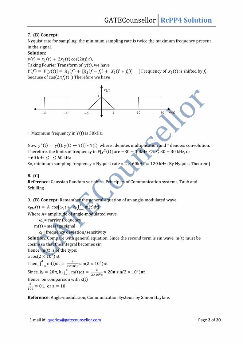
7. (B) Concept:
Nyquist rate for sampling: the minimum sampling rate is twice the maximum frequency present
in the signal.
Solution:
Taking Fourier Transform of , we have
( Frequency of is shifted by
because of ) Therefore we have
Maximum frequency in is 30kHz.
Now , where . denotes multiplication and * denotes convolution.
Therefore, the limits of frequency in are , or
So, minimum sampling frequency = Nyquist rate = (By Nyquist Theorem)
8. (C)
Reference: Gaussian Random variables, Principles of Communication systems, Taub and
Schilling
9. (B) Concept: Remember the general equation of an angle-modulated wave.
]
Where A= amplitude of angle-modulated wave
= carrier frequency
=message signal
=frequency deviation/sensitivity
Solution: Compare with general equation. Since the second term is sin wave, must be
cosine so that the integral becomes sin.
Hence, is of the type:
Then,
Since, ,
Hence, on comparison with x(t)
Reference: Angle-modulation, Communication Systems by Simon Haykins
5
1
f(kHz)
GATECounsellor RcPP4 Solution
E-mail id: [email protected] Page 3 of 20
10. (A) Concept:
An 8 bit DAC converts the 8 bit binary value in to analog value
The number of steps or difference level in N-bit DAC would be , where N signifies the size
of DAC( here N=8).
Hence steps size or Resolution= (let say)
Analog output value for input binary value=
Solution:-
Here R is not given. But we know, when i/p is analog o/p is 1 volt.
Hence =
………………………………….(.1)
Similarly
…………………………………….(2)
Dividing (2) by (1),
So, for input code , output voltage V
11. (A) Concept and Solution: All the statements are correct
a. HTL is designed from DTL gate with use of one zener diode. Zener diode is used to couple the
two transistor which increases noise immunity of gate.
b. DCTL exhibits current hogging phenomena. This is change in current at fixed output voltage
level because of absence of resistance in DCTL.
c. Problem of variable load is overcome by the totem pole arrangement.
12. (C) Concept: Instructions set of Microprocessor 8085 has following addressing modes
a. Immediate addressing mode ( ex. MVI B,FF))
b. Register direct addressing mode. (MOVE A,B)
c. Register indirect (XTHL, LDAX B)
d. Implicit (RRC, LLC)
Memory direct is type of Register addressing mode.
XTHL: Means Exchange HL with top of the stack pointer. Because of the pointer involvement this
instruction is called as Register indirect instruction.
Reference: Instruction set, 8085 Microprocessor by Gaonkar
13. (C) Concept: Static resistance is defined as .
14. (B)Concept: Class B has crossover distortion due to nonlinear current-voltage
characteristics of transistor.

GATECounsellor RcPP4 Solution
E-mail id: [email protected] Page 4 of 20
15. (B) Concept and Solution:
The phase shift constant of wave propagating in waveguide is
= β 21 ( / )cf f , Where fc is cut off frequency, β is phase shift constant of wave propagating
in free space.
We know that waveguide acts as high pass filter. So f > fc . Therefore < β.
It is also known that
, where is guide wavelength and is free space wavelength and is cutoff
wavelength of waveguide.
>λ.
16. (B) Concept and Solution:
For a homogeneous medium,2 /V
For Inhomogeneous medium, .( )V
Where is charge density and is permittivity.
17. (C) Solution: Image theory is applicable to problem involving Both Electrostatic field and
Magneto static field.
18. (B) Concept:
When a periodic signal in time domain is converted in to freq. domain the resultant transform
will be discrete (i.e. frequency is discrete.)
Periodicity TransformDiscreteness; Aperiodicity Transformcontinuousness
19. (B) Concept:- Duality Theorem of Fourier Transform
If then by duality (Replacing t by – and by t)
Solution: We know that,
by duality
As is an odd signal.
GATECounsellor RcPP4 Solution
E-mail id: [email protected] Page 5 of 20
20. (A) Concept:
I. Wave Explanation
i. Speech Speech is an 1-D varying signal .
ii. Image Image is a combination of 2-D pixels .
iii. T.V. Picture TV signal is a 3-D signal as 2-D image should be moved sequentially so
other dimension is required .
iv. Temperature Requires both space coordinates and time coordinate so .
21. (A) Concept: Herwitz Routh Criterion- For stable system first column of Herwitz table
should not change its sign. Number of times sign change is equal to number of poles in RHS.
Solution: Write the characteristic equation,
For no sign change we must have 3
Hence
22. (C) Concept:
The gain margin is a factor by which the gain of the system is allowed to increase before the
system reaches instability.
The phase margin of a stable system is the amount of additional phase lag required to bring the
system to bring it to the point of instability.
For stability both GM and PM should be positive. A system which has more positive GM and PM is
relatively more stable to system having lesser GM and PM.
; Phase margin is positive: Stable
or dB, PM : Marginally Stable
or dB (-ve), PM : Unstable ( -ve)
23. (B) Concept:
Low pass system:- System which blocks higher frequency value inputs
High pass system:- System which blocks lower frequency value inputs
All pass system:- System which allows all range of frequency value inputs to pass through or it
has symmetrical zero-pole about imaginary axis

GATECounsellor RcPP4 Solution
E-mail id: [email protected] Page 6 of 20
Minimum phase system:- Transfer function of these systems have neither poles nor zero on the
right hand side of the s-plane.
Solution:- By signal flow graph method transfer function of the given block diagram is
So All pass system. Since magnitude is 1 or since it has symmetrical pole-zero about
imaginary axis
24. (A) Concept:
i) Current and voltage are in phase in purely resistive circuit or in circuit where capacitive and
inductive reactance nullifies each other i.e. they are of equal magnitude.
ii) Current leads voltage in RC circuit or in circuit where capacitive reactance is higher than
inductive reactance.
iii) Current lags voltage in RL circuit or in circuit where inductive reactance is higher than
capacitive reactance.
iv) Z=impedance R=resistance
Solution: Current is leading then combination ,
Hence
Thus, this is correct combination. 25. (C) Concept: KVL and KCL
Solution: V be voltage across 5Ω resistor
The sum of current should be zero at or
So
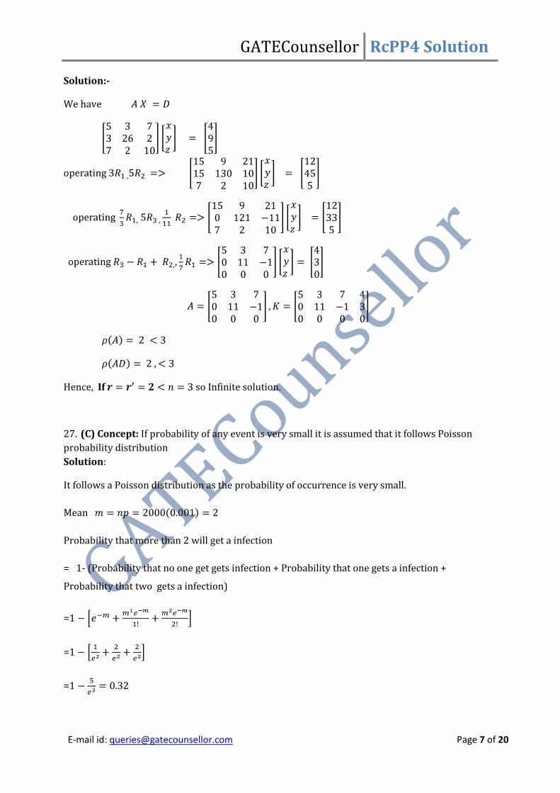
26. (C) Concept: A is coefficient matrix and K is augmented matrix ( it has LHS as last column in
coefficient matrix)
Let the rank of A be and that of K be and n is order of A
i) If the equations are inconsistent or it has no solution
ii) If the equations are consistent or it has unique solution
iii) If the equation are consistent or there are infinite number of solution
GATECounsellor RcPP4 Solution
E-mail id: [email protected] Page 7 of 20
Solution:-
We have
Hence, If so Infinite solution.
27. (C) Concept: If probability of any event is very small it is assumed that it follows Poisson
probability distribution
Solution:
It follows a Poisson distribution as the probability of occurrence is very small.
Mean
Probability that more than 2 will get a infection
= 1- (Probability that no one get gets infection + Probability that one gets a infection +
Probability that two gets a infection)
=
=
=
GATECounsellor RcPP4 Solution
E-mail id: [email protected] Page 8 of 20
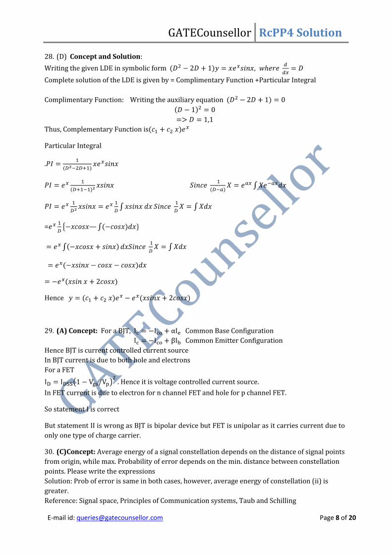
28. (D) Concept and Solution:
Writing the given LDE in symbolic form
Complete solution of the LDE is given by = Complimentary Function +Particular Integral
Complimentary Function: Writing the auxiliary equation
Thus, Complementary Function is
Particular Integral
.
= —
Hence
29. (A) Concept: For a BJT, Common Base Configuration
Common Emitter Configuration
Hence BJT is current controlled current source
In BJT current is due to both hole and electrons
For a FET
. Hence it is voltage controlled current source.
In FET current is due to electron for n channel FET and hole for p channel FET.
So statement I is correct
But statement II is wrong as BJT is bipolar device but FET is unipolar as it carries current due to
only one type of charge carrier.
30. (C)Concept: Average energy of a signal constellation depends on the distance of signal points
from origin, while max. Probability of error depends on the min. distance between constellation
points. Please write the expressions
Solution: Prob of error is same in both cases, however, average energy of constellation (ii) is
greater.
Reference: Signal space, Principles of Communication systems, Taub and Schilling

GATECounsellor RcPP4 Solution
E-mail id: [email protected] Page 9 of 20
31. (B) Concept: The extended source with source alphabet has Sn distinct blocks, where S is
the number of distinct symbols in source alphabet of the original source. In case of discrete
memoryless system, symbols are statistically independent. Hence, the probability of source
symbol in is equal to the product of the probabilities of the n source symbols in constituting
the particular source symbol in
And,
Solution:
Here, S0, S1, S2 having probabilities 0.25, 0.25 and 0.5 respectively.
So,
Symbols of source alphabet are,
S0S0 S0S1 S0S2 S1 S0 S1S1 S1S2 S2S0 S2S1 S2S2
0.25*0.25 0.25*0.25 0.25*0.5 0.25*0.25 0.25*0.25 0.25*0.5 0.5*0.25 0.5*0.25 0.5*0.5
bits
32. (C) Concept: Asynchronous counter
If N JK flip-flops are used counter repeats after . But if combinational circuit is also used
counter repeating after value less than can be designed. In this case counter is designed
so.
Solution:-Since NAND gate (combinational) is used counter repeats before 31. We have to look
for value which clears clear the JK flip flop.
At 10100 output of NAND gate will be ‘0’ which will clear the JK flip flop. Then it counts from
00000 again hence the Mod number is
33. (B) Concept: 2’s Compliment representation:- Two methods are used
1. When number is positive, magnitude is represented in true binary form and 0 is placed in MSB
to represent a positive number.
110 is +6
2. When the number is negative. The magnitude is written by 2’s compliment of the number and
1 is written in the place of MSB to represent it a negative number.
1010 is -6. How?
110 is +6 its 2’s compliment is 010, keeping 1 at MSB 1010 which is -6
By moving in reverse direction decimal equivalent of 2’s compliment number can be found.

GATECounsellor RcPP4 Solution
E-mail id: [email protected] Page 10 of 20
Solution:
In 2’s complement, the first bit represents the sign.
Take negative positional decimal equivalent of MSB bit.
Add with positional decimal value of other bits present. We get the value of numbers. (This is
shortcut)
1010 = -8+2 = -6
111010 = -32+16+8+2 = -6
11010 = -16+8+2 = -6
34. (D) Concept:
1. Objective is to select the chip
2. Check whether chip is active low or High
3. If active low then output of combinational circuit (here NAND gate) should be zero
4. If active high then output of combinational circuit (here NAND gate) should be 1.
Solution:
Our objective is to select the chip. To select the chip, we need to get the output as logic ‘0’ for
NAND gate as chip is active low.
8085 has 16 bit address bus.
Since the gate is NAND gate, the output will be logic ‘0’ only when all the inputs are logic ‘1’. But
here A15 is inverted before applying to the gate. So it should be logic ‘0’. So
A15=0,A14=1,A13=1;
A12=0 or 1 since it is given as don’t care. We need to check with the options given.
The remaining inputs A11……A0 are as follows
A11A10A9A8A7A6A5A4A3A2A1 A0 are varied as
0 0 0 0 0 0 0 0 0 0 0 0 which is equivalent to 000 H
1 1 1 1 1 1 1 1 1 1 1 1 which is equivalent to FFF H
Therefore, 6000 H-6FFF H or 7000 H -7FFF H satisfy the above conditions
Hence address range is 6000 H-7FFF H.
Reference: 8085 Microprocessor by Gaonkar

GATECounsellor RcPP4 Solution
E-mail id: [email protected] Page 11 of 20
35. (C) Concept: As is very large & finite, current in base can be assumed to be very small
since . Becomes significant because is very large.
Thevenin equivalent of such circuit has
Solution:- Thevenin equivalent of given circuit is
Now Since is very large
Now
Also in loop Collector to emitter

GATECounsellor RcPP4 Solution
E-mail id: [email protected] Page 12 of 20
36. (C) Concept and Solution:
Range of current
Transistors Q1 and Q2 are matched transistors with
is in active region if
Hence we have
Range of is
37. (B) Concept: AC analysis
Solution:
Short the capacitors & short the voltage sources

GATECounsellor RcPP4 Solution
E-mail id: [email protected] Page 13 of 20
Equivalent resistance seeing from emitter side
(Equivalent resistance seen from base side)
Angular frequency due to (since we have )
38. (C)Solution:
CMRR depends upon on both mismatch between transistors and resistance of the bias current
source.
39. (B) Concept and Solution:
The distance between adjacent voltage maxima is λ/2.
From the given data, λ/2 =15 cm. This implies λ= 30 cm.
Now, f = c/ λ = 1GHz.
40. (D) Concept and Solution:
Reflection Coefficient where and , ,
(assumption since nothing is given about this).
Therefore (air),
41. (B) Concept: Parseval’s Theorem
Solution: Since the Fourier transform is of form (2*a) / (a2 + 2). Its Inverse Fourier Transform
is exp(-a|t|) .
By
Hence by Parseval’s Theorem,

GATECounsellor RcPP4 Solution
E-mail id: [email protected] Page 14 of 20
42. (D) Concept :
When no information about system is given, we assume it is LTI (Linear,Time Invariant) system.
The output in LTI system is convolution of input and system function .
Therefore, where stands for convolution.
……………………………………(1)
Solution:
From the first block diagram
From the second block diagram
By eqn (1)
comparing with
Reference: Signals and Systems by Oppenheim.
43. (D) Concept and Solution: Application of Final value theorem and its constraints.
Final value theorem is applicable only when magnitude of poles is less than 1 except a simple
pole at .
Since one pole lies outside the unit circle, the system is unstable. Hence Final value theorem is
not applicable.
44. (C) Concept and solution: By Laplace transform of RLC circuit and KVL
So By comparative study we get

GATECounsellor RcPP4 Solution
E-mail id: [email protected] Page 15 of 20
45. (A) Concept and Solution: By KCL at each node
(When only are acting )
When and is acting
When and
When only
Solving we have,
46. (C) Concept:
Use Reciprocity theorem,
It is applicable only for single source network. It states that in a single source, linear bilateral
network the ratio of excitation to response remains same when position of the excitation and
response are interchanged.
47. (D)
48. (C) Concept and Solution:
If BJT is npn then in base region, minority carriers are electrons, whose concentration is given by
Now 10% of emitter doping concentration
By law of junction, we have,

GATECounsellor RcPP4 Solution
E-mail id: [email protected] Page 16 of 20
49. (D) Concept and Solution:
In order to have punch through the depletion region in base at base, collector junction must start
touching the depletion region in base at base emitter junction.
Now as width in a region
Initially we have
Now if we increase to then, in base depletion region of 45 is needed to cause punch
through,
So we must have
From (1) and (2)
50. (B) Concept and Solution:
Magnitude Criteria:
From fig (b), for all points on root locus
Given, P(-6,0) is on the root locus, it implies satisfy the above equation

GATECounsellor RcPP4 Solution
E-mail id: [email protected] Page 17 of 20
51. (B) Solution:
52. (B)Concept and Solution:
Information bit duration =
PN Chip duration =
Processing gain = = 4000
53. (C)Concept and Solution:
Jamming Margin (in dB) = Processing gain(in dB) -
Given,
Jamming Margin (in dB) =
Reference: Communication Systems by Simon Haykin, Chapeter 7, Page no: 479
54. (A) Concept and Solution: Equivalent Circuit
In general, this is a band pass filter.

GATECounsellor RcPP4 Solution
E-mail id: [email protected] Page 18 of 20
transfer function of a high pass filler
transfer function of a low pass filler
55. (A) Solution:
Clearly it will be a band reject filter.
56. (C)juggernaut: crush
Quisling (betrayer, who betray): betray
Taunt (to provoke): provoke
Juggernaut (over powerful, destructive object, who destroy): crush (to destroy)
Inception (commencement, beginning): termination (opposite meaning)
Obstinate (firmly or stubbornly adhering to one's purpose, opinion): preserve (to keep)
Hence close relation to given word is (C) juggernaut: crush
57. (B) yielding
Recalcitrant- hard to deal, not obedient
Yielding-flexible, hence the opposite word.
58. (D) New
Novice means a person new to some work or circumstances.
59. (A) an eloquent The second clause describes the discourses of a person as informative and inspirational, which gives us a clue that the missing blank should relate to informative and inspirational discourses. An eloquent speaker is the one whose discourses are informative and inspirational. Hence (A) is the answer. 60. (B) 0.38
Condition for contradiction: If true then lie or if lie true.
Thus answer is
61. (A) has never been applied, Congress is required to call a convention to consider
possible amendments to the document when formally asked to do so
Corrections are was never applied=>has never applied has been required=> is required for considering=> to consider
62. (B) 5min. late
Total travel time including rest time according to watch at home=from 2:35 pm to
4:00pm. =1hr 25 min
Total travel time excluding rest time = 1hr 25 min - 25 min=1hr=60min

GATECounsellor RcPP4 Solution
E-mail id: [email protected] Page 19 of 20
The speed during return to home was twice as that while going from home and hence the
time taken by the person to go office from home was twice that of going home from
office.
Thus ratio of time for going tooffice and coming from office and total time taken
only for travelling =60 min. min and min.
He took 40 min to go to office. Thus the time while he reached at office must be 2:35+40
min=3:15. But the time at office watch was 3:10. Hence the office watch was 5 min late.
63. (B) 28 ltr.
Let original milk in container is
After 4th operation quantity of milk present in the container lt. According
to the question, the ratio of quantity of milk to water after 4th operation is .
Thus, ratio of milk after 4th operation to the original milk amount
64. (C) 440
Considering relative speed, as A meets C every 88 seconds, then if C is at a constant point
then A covers the circular track in each 88 seconds. Same for B also which covers the
distance in 110 seconds.
With respect to C, speed of A, and that of B, . Relative speed of
A and B is
Where t is the time after which A meets B.
Thus
65. (C) 79
One line divides the whole space in to two and two lines into 4.
2 regions 4 regions 7 regions 11 regions
If no two lines are parallel and no three are concurrent, then 3rd line can cut the existing lines at most two places or three extra spaces are added. Thus 3 lines divide the whole space in to . One more line can intersect at most 3 points and will provide additional 4 spaces. The nth line can increase the region by k if and only if it divides k of the old regions and it divides k regions if and only if it intersects the existing lines at atmost points. 1 line region
2 lines regions
3 lines regions
4 lines regions

GATECounsellor RcPP4 Solution
E-mail id: [email protected] Page 20 of 20
n lines=2+2+3+4+…..+n regions=1+1+2+……+n-1+n regions=Sn+1
Where Sn is sum of n natural numbers number of non-overlapping regions inside the circle (as all intersects are inside
the circle, the total regions are inside the circle)=1+S12=1+78=79