gandhi institute of technology and …...code title 1 eec702 vlsi cad ce 3 1 0 4 2 eec704 vlsi dsp...
TRANSCRIPT

GANDHI INSTITUTE OF TECHNOLOGYAND MANAGEMENT
(GITAM)(Deemed to be University, Estd. u/s 3 of UGC Act 1956)VISAKHAPATNAM HYDERABAD BENGALURU
Accredited by NAAC with ‘A’ Grade
REGULATIONS AND SYLLABUSof
Master of Technologyin
VLSI Design(w.e.f 2015-16 admitted batch)
A University Committed to ExcellenceA University Committed to Excellence

VISIONTo become a global leader in higher education.
MISSIONTo impart futuristic and comprehensive
education of global standards education of global standards with a high sense of discipline and
social relevance in a serene and invigorating environment.

GANDHI INSTITUTE OF TECHNOLOGYAND MANAGEMENT
(GITAM)(Declared as Deemed to be University U/S 3 of UGC Act, 1956)
VISAKHAPATNAM * HYDERABAD * BENGALURUAccredited by NAAC with ‘A’ Grade
REGULATIONS AND SYLLABUSOF
Master of Technologyin
VLSI Design(w.e.f 2015 -16 admitted batch)
A University Committed to Excellence

1
M.Tech. in VLSI DesignREGULATIONS
(w.e.f. 2015-16 admitted batch)
1. ADMISSION
1.1 Admission into M.Tech. in VLSI Design program of GITAMUniversity is governed by GITAM University admission regulations.
2. ELIGIBILITY CRITERIA
2.1 A pass in B.E./B.Tech./AMIE in ECE / EEE / EIE / Instrumentation/ CSE / IT or its equivalent.
2.2 Admissions into M.Tech. will be based on the following:
(i) Score obtained in GAT (PG), if conducted.
(ii) Performance in Qualifying Examination / Interview.
2.3 The actual weightage to be given to the above items will be decidedby the authorities before the commencement of the academic year.Candidates with valid GATE score shall be exempted from appearingfor GAT (PG).
3. CHOICE BASED CREDIT SYSTEM
3.1 Choice Based Credit System (CBCS) is introduced with effect fromthe admitted Batch of 2015-16 based on UGC guidelines in orderto promote:
• Student Centered Learning• Cafeteria approach• Students to learn courses of their choice• Learning at their own pace• Inter-disciplinary learning
3.2 Learning goals/ objectives and outcomes are specified leading towhat a student should be able to do at the end of the program.
4. STRUCTURE OF THE PROGRAM
4.1 The Program Consists of
i) Core Courses (compulsory) which give general exposure to aStudent in VLSI Design and subject related area.
ii) Programme Electives.
iii) Open Electives.
2
4.2 Each course is assigned a certain number of credits depending uponthe number of contact hours (lectures/tutorials/practical) per week.
4.3 In general, credits are assigned to the courses based on thefollowing contact hours per week per semester.• One credit for each Lecture / Tutorial hour per week.• One credit for two hours of Practicals per week.• Two credits for three (or more) hours of Practicals per week.
5. MEDIUM OF INSTRUCTION
The medium of instruction (including examinations and projectreports) shall be English.
6. REGISTRATION
Every student has to register himself/herself for each semesterindividually at the time specified by the Institute / University.
7. ATTENDANCE REQUIREMENTS
7.1 A student whose attendance is less than 75% in all the courses puttogether in any semester will not be permitted to attend the end- semester examination and he/she will not be allowed to registerfor subsequent semester of study. He/she has to repeat the semesteralong with his / her juniors.
7.2 However, the Vice Chancellor on the recommendation of thePrincipal / Director of the Institute/School may condone the shortageof attendance to the students whose attendance is between 66% and74% on genuine grounds and on payment of prescribed fee.
8. EVALUATION
8.1 The assessment of the student’s performance in a Theory courseshall be based on two components: Continuous Evaluation (40marks) and Semester-end examination (60 marks).
8.2 A student has to secure an aggregate of 40% in the course in thetwo components put together to be declared to have passed thecourse, subject to the condition that the candidate must havesecured a minimum of 24 marks (i.e. 40%) in the theory componentat the semester-end examination.
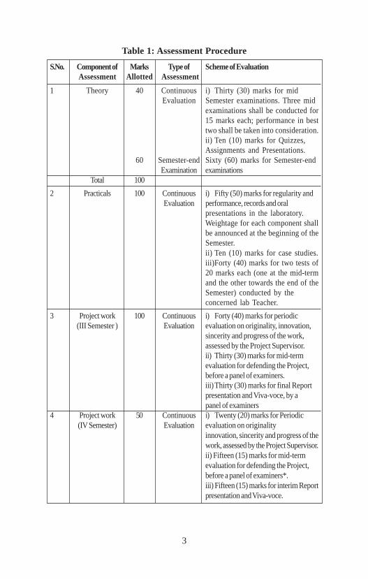
8.3 Practical/ Project Work/ Industrial Training/ Viva voce/ Seminar etc.course are completely assessed under Continuous Evaluation fora maximum of 100 marks, and a student has to obtain a minimumof 40% to secure Pass Grade. Details of Assessment Procedure arefurnished below in Table 1.
3
Table 1: Assessment Procedure
S.No. Component of Marks Type of Scheme of EvaluationAssessment Allotted Assessment
1 Theory 40 Continuous i) Thirty (30) marks for midEvaluation Semester examinations. Three mid
examinations shall be conducted for15 marks each; performance in besttwo shall be taken into consideration.ii) Ten (10) marks for Quizzes,Assignments and Presentations.
60 Semester-end Sixty (60) marks for Semester-endExamination examinations
Total 100
2 Practicals 100 Continuous i) Fifty (50) marks for regularity andEvaluation performance, records and oral
presentations in the laboratory.Weightage for each component shallbe announced at the beginning of theSemester.ii) Ten (10) marks for case studies.iii)Forty (40) marks for two tests of20 marks each (one at the mid-termand the other towards the end of theSemester) conducted by theconcerned lab Teacher.
3 Project work 100 Continuous i) Forty (40) marks for periodic(III Semester ) Evaluation evaluation on originality, innovation,
sincerity and progress of the work,assessed by the Project Supervisor.ii) Thirty (30) marks for mid-termevaluation for defending the Project,before a panel of examiners.iii)Thirty (30) marks for final Reportpresentation and Viva-voce, by apanel of examiners
4 Project work 50 Continuous i) Twenty (20) marks for Periodic(IV Semester) Evaluation evaluation on originality
innovation, sincerity and progress of thework, assessed by the Project Supervisor.ii) Fifteen (15) marks for mid-termevaluation for defending the Project,before a panel of examiners*.iii) Fifteen (15) marks for interim Reportpresentation and Viva-voce.

4
50 Semester-end Fifty (50) marks for final ReportExamination presentation and Viva-voce assessed by
external examiners.Total 100
5 Comprehensive 100 Continuous Through five periodic Viva-voce exams forViva-voce Evaluation 20 marks each, conducted by a panel
(II Semester) of examiners. The course contentfor Viva exams shall be announced at thebeginning of the Semester.
*Panel of Examiners shall be appointed by the concerned Head of the Department
9. REAPPEARANCE
9.1 A student who has secured ‘F’ grade in a Theory course shall haveto reappear at the subsequent Semester end examination held forthat course.
9.2 A student who has secured ‘F’ grade in a Practical course shall haveto attend Special Instruction Classes held during summer.
9.3 A student who has secured ‘F’ Grade in Project work / IndustrialTraining etc shall have to improve his/her report and reappear forViva – voce at the time of Special Examination to be conductedin the summer vacation.
10. SPECIAL EXAMINATION
10.1 A student who has completed his/her period of study and still has“F” grade in a maximum of three theory courses is eligible to appearfor Special Examination normally held during summer vacation.
11. BETTERMENT OF GRADES
A student who has secured only a Pass or Second class and desiresto improve his/her Class can appear for Betterment Examinationsonly in Theory courses of any Semester of his/her choice, conductedin Summer Vacation along with the Special Examinations.Betterment of Grades is permitted ‘only once’ immediately aftercompletion of the program of study.
12. GRADING SYSTEM
12.1 Based on the student performance during a given semester, a finalletter grade will be awarded at the end of the semester in eachcourse. The letter grades and the corresponding grade points areas given in Table 2.

5
Table 2: Grades & Grade Points
Sl.No. Grade Grade Points Absolute Marks1 O (outstanding) 10 90 and above
2 A+ (Excellent) 9 80 to 89
3 A (Very Good) 8 70 to 79
4 B+ (Good) 7 60 to 69
5 B (Above Average) 6 50 to 59
6 C (Average) 5 45 to 49
7 P (Pass) 4 40 to 44
8 F (Fail) 0 Less than 40
9 Ab. (Absent) 0 -
12.2 A student who earns a minimum of 4 grade points (P grade) in acourse is declared to have successfully completed the course, andis deemed to have earned the credits assigned to that course, subjectto securing a GPA of 5 for a Pass in the semester.
13. GRADE POINT AVERAGE
13.1 A Grade Point Average (GPA) for the semester will be calculatedaccording to the formula:
Σ [ C X G ]GPA = ——————
Σ CWhere
C = number of credits for the course,G = grade points obtained by the student in the course.
13.2 To arrive at Cumulative Grade Point Average (CGPA), a similarformula is used considering the student’s performance in all thecourses taken, in all the semesters up to the particular point of time.
13.3 CGPA required for classification of class after the successfulcompletion of the program is shown in Table 3.
Table 3: CGPA required for award of Class
Class CGPA Required
First Class with Distinction > 8.0*
First Class > 6.5
Second Class > 5.5
Pass Class > 5.0
* In addition to the required CGPA of 8.0 or more, the student must havenecessarily passed all the courses of every semester in first attempt.

6
14. ELIGIBILITY FOR AWARD OF THE M.Tech. DEGREE
14.1 Duration of the program: A student is ordinarily expected tocomplete the M.Tech. program in four semesters of two years.However a student may complete the program in not more thanfour years including study period.
14.2 However the above regulation may be relaxed by the ViceChancellor in individual cases for cogent and sufficientreasons.
14.3 A student shall be eligible for award of the M.Tech. Degreeif he / she fulfills all the following conditions.
a) Registered and successfully completed all the coursesand projects.
b) Successfully acquired the minimum required credits asspecified in the curriculum corresponding to the branchof his/her study within the stipulated time.
c) Has no dues to the Institute, hostels, Libraries, NCC /NSS etc, and
d) No disciplinary action is pending against him / her.
15. DISCRETIONARY POWER
Not withstanding anything contained in the above sections, theVice Chancellor may review all exceptional cases, and give hisdecision, which will be final and binding.

7
M.Tech. in VLSI DesignDepartment of Electronic and Communication Engineering
Effective from academic year 2015-2016 admitted batch
Semester I
S.No. Course Course Category L T P CCode Title
1 EEC701 Digital System Design CE 3 1 0 4
2 EEC703 Digital IC Design CE 3 1 0 4
3 EEC705 Analog IC Design CE 3 1 0 4
4 EEC707 VLSI Technology CE 3 1 0 4
5 EEC7XX Program Elective – I PE 3 1 0 4
6 EYYXXX Open Elective – I OE 3 0 0 3
7 EEC721 VLSI Circuit DesignLaboratory CE 0 0 3 2
8 EEC723 FPGA DesignLaboratory CE 0 0 3 2
27
Semester II
S.No. Course Course Category L T P CCode Title
1 EEC702 VLSI CAD CE 3 1 0 4
2 EEC704 VLSI DSP Architectures CE 3 1 0 4
3 EEC706 ASIC Design CE 3 1 0 4
4 EEC7XX Program Elective –II PE 3 1 0 4
5 EEC7XX Program Elective – III PE 3 1 0 4
6 EYYXXX Open Elective – II 3 0 0 3
7 EEC722 Advanced VLSI DesignLaboratory CE 0 0 3 2
8 EEC792 Technical Seminar CE 0 0 3 2
9 EEC794 ComprehensiveViva Voce CE 2
29

8
Semester III
S.No. Course Course Category L T P CCode Title
1 EEC 891 Project Work CE 8
8
Semester IV
S.No. Course Course Category L T P CCode Title
1 EEC892 Project work CE 16
16
Number of Credits
Semester I II III IV Total
Credits 27 29 8 16 80
Open Elective-I
S.No. Course Course Category L T P CCode Title
1. ECS781 Web Technologies OE 3 0 0 3
2. ECS783 Linux Programming andScripting OE 3 0 0 3
3. ECS785 Programming with Java OE 3 0 0 3
4. ECS787 Data Structures andAlgorithms OE 3 0 0 3
5. ECS789 Operating Systems OE 3 0 0 3
Open Elective-II
S.No. Course Course Category L T P CCode Title
1. EEI780 Circuits for AnalogSystem Design OE 3 0 0 3
2. ECS782 Computer Arithmetic OE 3 0 0 3
3. EEI762 Modern Digital OE 3 0 0 3Signal Processing
4. ECS784 Computer Architecture OE 3 0 0 3
5. EEC753 Embedded SystemDesign OE 3 0 0 3
6. EEI782 ARM SystemDevelopment OE 3 0 0 3

9
PROGRAMME ELECTIVES
Programme Elective - I
S.No. Course Course Category L T P CCode Title
1 EEC767 Modeling and Design PE 3 1 0 4with HDLs
2 EEC741 Active Filter Design PE 3 1 0 4
3 EEC740 Semiconductor Devices PE 3 1 0 4
4 EEC750 Digital Signal Processing PE 3 1 0 4with FPGAs
5 EEC713 DSP Processors and PE 3 1 0 4Architectures
6 EEC742 Advanced Computer PE 3 1 0 4Organization
Programme Elective-II
S.No. Course Course Category L T P CCode Title
1 EEC776 RF IC Design PE 3 1 0 4
2 EEC762 Low Power VLSI Design PE 3 1 0 4
3 EEC752 Digital Systems Testing and PE 3 1 0 4Testability
4 EEC751 Digital Systems Engineering PE 3 1 0 4
5 EEC747 Broadband Communication PE 3 1 0 4Circuits
6 EEC771 Operation and Modeling of PE 3 1 0 4MOS Transistor

10
Programme Elective - III
S.No. Course Course Category L T P CCode Title
1 EEC748 Data Converters PE 3 1 0 4
2 EEC743 Advanced Digital PE 3 1 0 4IC Design
3 EEC783 VLSI Physical Design PE 3 1 0 4Automation
4 EEC761 Logic Synthesis and PE 3 1 0 4Verification
5 EEC779 Signal ProcessingTechniques PE 3 1 0 4for Software Radios
6 EEC787 Advanced LogicSynthesis PE 3 1 0 4

11
EEC701: DIGITAL SYSTEM DESIGNL T P C3 1 0 4
Module I 10 HoursReview of Logic Design Fundamentals: Combinational logic, Boolean algebraand algebraic Simplification Karnaugh maps, designing with NAND and NORgates, hazards in combinational circuits, flip-flops and latches, Mealy sequentialcircuit design, design of a Moore sequential circuit, equivalent states and reductionof state tables, sequential circuit timing, tristate logic and busses.Module II 10 HoursIntroduction to VHDL: Computer-aided design, hardware description languages,VHDL description of combinational circuits, VHDL modules, sequentialstatements and VHDL processes, modeling flip-flops using VHDL processes,processes using wait statements, two types of VHDL delays: Transport andinertial delays, compilation, simulation, and synthesis of VHDL code, VHDLdata types and operators, simple synthesis examples, VHDL models formultiplexers, VHDL libraries, modeling registers and counters using VHDLprocesses, behavioral and structural VHDL, variables, signals, and constants,arrays, loops in VHDL, assert and report statements.Module III 10 HoursIntroduction to Programmable Logic Devices: Brief overview of programmablelogic devices, simple programmable logic devices (SPLDs), complex programmablelogic devices (CPLDs), field-programmable gate arrays (FPGAs), DesignExamples: BCD to 7-segment display decoder, a BCD adder, 32-bit adders,traffic light controller, state graphs for control circuits, scoreboard and controller,synchronization and debouncing, a shift-and-add multiplier, array multiplier, asigned integer/ fraction multiplier/ keypad scanner/ binary dividers.Module IV 10 HoursSM Charts and Microprogramming: State machine charts, derivation of SMcharts, realization of SM charts, implementation of the dice game,microprogramming, linked state machines.Module V 10 HoursDesigning with Field Programmable Gate Arrays: Implementing functionsin FPGAs, implementing functions using Shannon’s decomposition, carry chainsin FPGAs, cascade chains in FPGAs, examples of logic blocks in commercialFPGAs, dedicated memory in FPGAs, dedicated multipliers in FPGAs, cost ofprogrammability, FPGAs and One-Hot state assignment, FPGA capacity:Maximum Gates Versus Usable Gates, design translation (synthesis), mapping,placement, and routing.
Text Book(s)1. Charles Roth, Digital Systems Design using VHDL, 2/e, Cengage Learning, 2012.References1. John F. Wakerly, Digital Design Principles and Practices, 4/e, Pearson Education,
2013.2. Michael Ciletti, Advanced Digital Design using Verilog HDL, 2/e, Prentice Hall
Publications, 2012.3. Stephen Brown, ZvonkoVranesic, Fundamentals of Digital Logic with Verilog
Design, 2/e, Tata McGraw Hill Publishers, 2014.

12
EEC702: VLSI CADL T P C3 1 0 4
Module I 10 HoursAlgorithmic Graph Theory and Computational Complexity – Terminology,data structures for the representation of graphs, computational complexity,examples of graph algorithms, depth-first search, breadth-first search, Dijkstra'sshortest-path algorithm, Prim's algorithm for minimum spanning trees. Tractableand Intractable Problems: Combinatorial optimization problems, decisionproblems, complexity classes, NP-completeness and NP-hardness.
Module II 10 HoursSimulation: Gate-level modeling and simulation, signal modeling, gate modeling,delay modeling, connectivity modeling, compiler-driven simulation event-drivensimulation, switch-level modeling and simulation, connectivity and signal modeling,simulation mechanisms.
Module III 10 HoursLogic Synthesis and Verification: Introduction to combinational logic synthesis,basic issues and terminology, a practical example, binary-decision diagrams,ROBDD principles, ROBDD implementation and construction, ROBDDmanipulation, variable ordering, applications to verification, applications tocombinatorial optimization. High-level Synthesis: Hardware models for high-levelsynthesis, hardware for computations, data storage, and interconnection, data,control, and clocks, internal representation of the input algorithm, allocation,assignment and scheduling, some scheduling algorithms, some aspects of theassignment problem.
Module IV 10 HoursLayout Compaction: Design rules, symbolic layout, problem formulation,algorithms for constraint-graph compaction, a longest-path algorithm for DAGs,the longest path in graphs with cycles, the Liao - Wong algorithm, the Bellman-Ford algorithm, discussion: shortest paths, longest paths and time complexity,other issues. Placement and Partitioning: Circuit representation, wire-lengthestimation, types of placement problem, placement algorithms, constructiveplacement, iterative improvement, partitioning, the Kernighan-Lin partitioningalgorithm.
Module V 10 HoursFloorplanning:Floorplanning concepts, terminology and floorplan representation,optimization problems in floorplanning, shape functions and floorplan sizing.Routing: Types of local routing problems, area routing, channel routing, channelrouting models, the vertical constraint graph, horizontal constraints and the left-edge algorithm, channel routing algorithms, introduction to global routing,standard-cell layout, building-block layout and channel ordering, algorithms forglobal routing, problem definition and discussion, efficient rectilinear Steiner-treeconstruction, local transformations for global routing.

13
Text Book(s)
1. S. H. Gerez, Algorithms for VLSI Design Automation, WILEY Student Edition,India, 2013.
References
1. Majid Sarrafzadeh and C, K, Wong, An Introduction to VLSI Physical Design,McGraw Hill, 2011.
2. Naveed Sherwani, Algorithms for VLSI Physical Design Automation, 3/e,Kluwer Academic, 2012.
3. Sung Kyu Lim, Practical Problems in VLSI Physical Design Automation,Springer Publications, 2011.
14
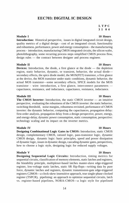
EEC703: DIGITAL IC DESIGN
L T P C 3 1 0 4
Module I 10 HoursIntroduction: Historical perspective, issues in digital integrated circuit design,quality metrics of a digital design - cost of an integrated circuit, functionalityand robustness, performance, power and energy consumption – the manufacturingprocess - introduction, manufacturing CMOS integrated circuits, the silicon wafer,photolithography, some recurring process steps simplified CMOS process flow,design rules — the contract between designer and process engineer.
Module II 10 HoursDevices: Introduction, the diode, a first glance at the diode — the depletionregion, static behavior, dynamic, or transient, behavior, the actual diode—secondary effects, the spice diode model, the MOS(FET) transistor, a first glanceat the device, the MOS transistor under static conditions, dynamic behavior, theactual MOS transistor—some secondary effects, SPICE models for the MOStransistor – wire: introduction, a first glance, interconnect parameters —capacitance, resistance, and inductance, capacitance, resistance, inductance.
Module III 10 HoursThe CMOS Inverter: Introduction, the static CMOS inverter — an intuitiveperspective, evaluating the robustness of the CMOS inverter: the static behavior,switching threshold, noise margins, robustness revisited, performance of CMOSinverter: the dynamic behavior, computing the capacitances, propagation delay:first-order analysis, propagation delay from a design perspective, power, energy,and energy-delay, dynamic power consumption, static consumption, perspective:technology scaling and its impact on the inverter metrics.
Module IV 10 HoursDesigning Combinational Logic Gates in CMOS: Introduction, static CMOSdesign, complementary CMOS, ratioed logic, pass-transistor logic, dynamicCMOS design, dynamic logic: basic principles, speed and power dissipationof dynamic logic, issues in dynamic design, cascading dynamic gates, perspectives,how to choose a logic style, designing logic for reduced supply voltages.
Module V 10 HoursDesigning Sequential Logic Circuits: Introduction, timing metrics forsequential circuits, classification of memory elements, static latches and registers,the bistability principle, multiplexer-based latches master-slave edge-triggeredregister, low-voltage static latches, static SR flip-flops—writing data by pureforce, dynamic latches and registers, dynamic transmission-gate edge-triggeredregisters C2MOS—a clock-skew insensitive approach, true single-phase clockedregister (TSPCR), pipelining: an approach to optimize sequential circuits, latchvs. register-based pipelines, NORA-CMOS—a logic style for pipelined
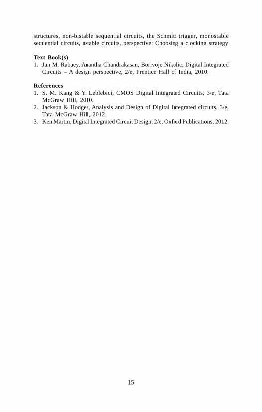
15
structures, non-bistable sequential circuits, the Schmitt trigger, monostablesequential circuits, astable circuits, perspective: Choosing a clocking strategy
Text Book(s)1. Jan M. Rabaey, Anantha Chandrakasan, Borivoje Nikolic, Digital Integrated
Circuits – A design perspective, 2/e, Prentice Hall of India, 2010.
References1. S. M. Kang & Y. Leblebici, CMOS Digital Integrated Circuits, 3/e, Tata
McGraw Hill, 2010.2. Jackson & Hodges, Analysis and Design of Digital Integrated circuits, 3/e,
Tata McGraw Hill, 2012.3. Ken Martin, Digital Integrated Circuit Design, 2/e, Oxford Publications, 2012.
16
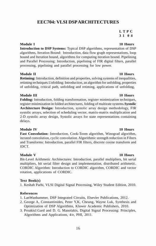
EEC704: VLSI DSP ARCHITECTURES
L T P C3 1 0 4
Module I 10 HoursIntroduction to DSP Systems: Typical DSP algorithms, representation of DSPalgorithms, Iteration Bound: Introduction, data flow graph representations, loopbound and Iteration bound, algorithms for computing iteration bound. Pipeliningand Parallel Processing: Introduction, pipelining of FIR digital filters, parallelprocessing, pipelining and parallel processing for low power.
Module II 10 HoursRetiming: Introduction, definition and properties, solving systems of inequalities,retiming techniques.Unfolding: Introduction, an algorithm for unfolding, propertiesof unfolding, critical path, unfolding and retiming, applications of unfolding,
Module III 10 HoursFolding: Introduction, folding transformation, register minimization techniques,register minimization in folded architectures, folding of multirate systems.SystolicArchitecture Design: Introduction, systolic array design methodology, FIRsystolic arrays, selection of scheduling vector, matrix-matrix multiplication and2-D systolic array design, Systolic arrays for state representations containingdelays.
Module IV 10 HoursFast Convolution: Introduction, Cook-Toom algorithm, Winograd algorithm,iterated convolution, cyclic convolution. Algorithmic strength reduction in Filtersand Transforms: Introduction, parallel FIR filters, discrete cosine transform andIDCT.
Module V 10 HoursBit-Level Arithmetic Architectures: Introduction, parallel multipliers, bit serialmultipliers, bit serial filter design and implementation, distributed arithmetic.CORDIC Algorithm: Introduction to CORDIC algorithm, CORDIC and vectorrotation, applications of CORDIC.
Text Book(s)1. Keshab Parhi, VLSI Digital Signal Processing, Wiley Student Edition, 2010.
References1. LanWanhammer, DSP Integrated Circuits, Elsevier Publications, 2012.2. George A, Constantinides, Peter Y,K, Cheung, Wayne Luk, Synthesis and
Optimization of DSP Algorithms, Kluwer Academic Publishers, 2010.3. ProakisJ.Gard and D. G. Manolakis, Digital Signal Processing: Principles,
Algorithms and Applications, 4/e, PHI, 2011.

17
EEC705: ANALOG IC DESIGNL T P C3 1 0 4
Module I 10 HoursBasic MOS Device Physics: General considerations, MOSFET as a switch,MOSFET structure, MOS symbols, MOS I/V characteristics, threshold voltage,derivation of I/V characteristics, second-order effects, MOS device models, MOSdevice layout, MOS device capacitances, MOS small-signal model, MOS SPICEmodels, NMOS versus PMOS devices, long-channel versus short-channel devices.
Module II 10 HoursSingle-Stage Amplifiers: Basic concepts, common-source stage, common-sourcestage with resistive load, CS stage with diode-connected load, CS stage withcurrent-source load, CS stage with triode load, CS stage with source degeneration,source follower, common-gate stage, cascode stage, folded cascode, choice ofdevice models.
Module III 10 HoursDifferential Amplifiers: Single-ended and differential operation, basic differentialpair, qualitative analysis, quantitative analysis, common-mode response,differential pair with MOS loads, gilbert cell. Passive and Active CurrentMirrors: Basic current mirrors, cascode current mirrors, active current mirrors,large-signal analysis, small-signal analysis, common-mode properties.
Module IV 10 HoursFrequency Response of Amplifiers: General considerations, Miller effect,association of poles with nodes, common-source stage, source followers, common-gate stage, cascode stage, differential pair. Feedback: General considerations,properties of feedback circuits, types of amplifiers, feedback topologies, voltage-voltage feedback, current-voltage feedback, voltage-current feedback, current-current feedback, effect of loading, two-port network models, loading in voltage-voltage feedback.
Module V 10 HoursOperational Amplifiers: General considerations, performance parameters, one-stage op amps, two-stage op amps, gain boosting, comparison, common-modefeedback, input range limitations, slew rate, power supply rejection. Stabilityand Frequency Compensation: General considerations, multipole systems,phase margin, frequency compensation, compensation of two-stage op amps,slewing in two-stage op amps.
Text Book(s)1. B. Razavi, Design of Analog CMOS Integrated Circuits, McGraw Hill, 2002.References1. P. R. Gray & R. G. Meyer, Analysis and Design of Analog Integrated Circuits,
5/e, John Wiley, 2012.2. Ken Martin, Analog Integrated Circuit Design, 2/e, Wiley Publications, 2012.3. Sedra and Smith, Microelectronic Circuits, 6/e, Oxford Publications, 2014.

18
EEC706: ASIC DESIGNL T P C3 1 0 4
Module I 10 HoursTypes of ASICs : Full-Custom ASICs, Standard-Cell-Based ASICs, Gate-Array-Based ASICs, Channeled Gate Array, Channelless Gate Array, Structured GateArray, Programmable Logic Devices, Field-Programmable Gate Arrays, DesignFlow, Case Study, ASIC Cell Libraries, CMOS Logic: CMOS Transistors,Combinational Logic Cells, Sequential Logic Cells, Datapath Logic Cells, IO Cells,ASIC Library Design:Transistors as Resistors, Transistor Parasitic Capacitance,Library-Cell Design, Library Architecture, Gate-Array Design, Standard-CellDesign, Datapath-Cell Design.
Module II 10 HoursVerilog: Basics of the Verilog Language, Operators, Hierarchy, Procedures andAssignments, Timing Controls and Delay, Tasks and Functions, ControlStatements, Logic-Gate Modeling, Modeling Delay, Altering Parameters, LogicSynthesis:A Logic-Synthesis Example, A Comparator/MUX, Inside a LogicSynthesizer, Synthesis of the Viterbi Decoder, Verilog and Logic Synthesis,Performance Driven Synthesis.
Module III 10 HoursSimulation: Types of Simulation, The Comparator/MUX Example, LogicSystems, How Logic Simulation Works, Cell Models, Delay Models, StaticTiming Analysis, Formal Verification, Switch-Level Simulation, Transistor-LevelSimulation, Test: The Importance of Test, Boundary-Scan Test, Faults, FaultSimulation, Automatic Test-Pattern Generation, Scan Test, Built-in Self-test, ASimple Test Example.
Module IV 10 HoursASIC Construction: Physical Design, CAD Tools, System Partitioning,Estimating ASIC Size, Power Dissipation, FPGA Partitioning, PartitioningMethods.
Module V 10 HoursFloorplanning and Placement: Floorplanning, Placement, Physical Design Flow,Information Formats, Routing: Global Routing, Detailed Routing, Special Routing,Circuit Extraction and DRC.
Text Book(s)1. Michael John Sebastian Smith, Application-Specific Integrated Circuits,
Pearson Education, 2012References1. SabihGerez, Algorithms for VLSI Design Automation, Wiley Publications,
2012.2. Wayne Wolf, Modern VLSI Design 3/e, Pearson Education, 2014.3. Samir Palnitkar, Verilog HDL 2/e, Pearson Education, 2012.

19
EEC707: VLSI TECHNOLOGYL T P C3 1 0 4
Module I 10 HoursIntroduction: Semiconductor materials, semiconductor devices, semiconductorprocess technology, basic fabrication steps. Crystal growth: Silicon crystal growthfrom melt, silicon float-zone process, GaAs crystal growth techniques, materialcharacterization.
Module II 10 HoursSilicon Oxidation: Thermal oxidation, impurity redistribution during oxidation,masking properties of silicon dioxide, oxide quality, oxide thicknesscharacterization. Photolithography: Optical lithography, next-generationlithography.
Module III 10 HoursEtching: Wet chemical etching, Dry etching. Diffusion: Basic diffusion process,extrinsic diffusion, lateral diffusion.
Module IV 10 HoursIon Implantation: Range of implanted ions, implant damage and annealing,implantation-related process. Film Deposition: Epitaxial growth techniques,structures and defects in epitaxial layers, dielectric deposition, polysilicondeposition, metallization.
Module V 10 HoursProcess Integration: Passive components, Bipolar technology, MOSFETtechnology, MESFET technology, MEMS technology. IC Manufacturing:Electrical testing, Packaging.
Text Book(s)1. Gary S May & Simon M Sze, Fundamentals of Semiconductor Fabrication,
Wiley Student Edition, 2012.
References1. S. K. Ghandhi, VLSI Fabrication Principles, John Wiley Inc, 2010.2. S. M. Sze, VLSI Technology, 2/e, McGraw Hill, 2011.3. Stephen Cambell, The Science and Engineering of Microelectronic Fabrication,
Oxford University Press, 2013.

20
ECS781: WEB TECHNOLOGIESL T P C3 0 0 3
Module I 8 hoursIntroduction to HTML Version5: Basic syntax, HTML document structure,text formatting, images, lists, links, tables, forms, frames, section, article, rangeand date. Cascading Style Sheets Version3: Levels of style sheets, stylespecification formats, selector forms, font properties, list properties, colorproperties, alignment of text, background images, span and div tags.
Module II 10 hoursIntroduction to Java Script: Overview of java script, syntactic characteristics,primitives, operator and expression, control statements, arrays, functions, errorsin scripts, Document Object Model(DOM), event driven computation, elementaccess in java script, the navigator object. Dynamic Document with Java Script: Element positioning, moving elements, changing colors and fonts, dynamiccontent, locating the mouse cursor, slow movements of elements, dragging anddropping elements.
Module III 8 hoursIntroduction to XML: Syntax of XML, document structure, and document typedefinition, namespaces, XML schemas, document object model, presenting XMLusing CSS. Introduction to other XML Technologies: XLink, XPointer, XQueryand XPath, XQuery and XSLT, XQuery processor and FLWOR expression.
Module IV 8 hoursIntroduction to Servlets: Lifecycle of a servelet, the servlet API, thejavax.servelet package, the javax.servlet.http package, handling http request &responses, using cookies, session tracking and security issues and servlets withdatabase connectivity. Introduction to Model View Controller (MVC):Architecture, its structure, components.
Module V 8 hoursIntroduction to JSP: The problem with servlet, the anatomy of a JSP page,JSP processing, JSP applications, JSP components, comments, expressions,scriplets, JSTL tag library, JSP database connectivity. Introduction to Web Servers:Installing the Java software development kit, tomcat server & testing tomcat,structure of web application, deploying web application, IIS web server, andGWS web server.
Text Book(s)1. Robert W.Sebesta, Programming the World Wide Web, 4/e, Pearson, 2007.2. Chris Bates, Web Technologies, 2/e, Wiley, 2002.3. Jason Hunter, William Crawford, Java Servlet Programming, 2/e, O'Reilly,
2003.

21
References1. Dietel and Nieto, Internet and World Wide Web – How to program, PHI/
Pearson Education, 2006.2. Herbert Schildt, JAVA The Complete References, 8/e, McGraw Hill, 20143. UttamK.Roy, Web Technologies, Oxford Higher Education publication, 2004.4. BaiEkedaw, Web Warrior Guide to Web Programmming, Thompson
Publications, 2012.
22
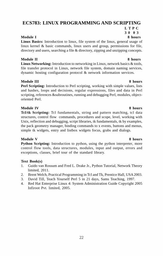
ECS783: LINUX PROGRAMMING AND SCRIPTINGL T P C3 0 0 3
Module I 8 hoursLinux Basics: Introduction to linux, file system of the linux, general usage oflinux kernel & basic commands, linux users and group, permissions for file,directory and users, searching a file & directory, zipping and unzipping concepts.
Module II 8 hoursLinux Networking: Introduction to networking in Linux, network basics & tools,file transfer protocol in Linux, network file system, domain naming services,dynamic hosting configuration protocol & network information services.
Module III 8 hoursPerl Scripting: Introduction to Perl scripting, working with simple values, listsand hashes, loops and decisions, regular expressions, files and data in Perlscripting, references &subroutines, running and debugging Perl, modules, object-oriented Perl.
Module IV 8 hoursTcl/tk Scripting: Tcl fundamentals, string and pattern matching, tcl datastructures, control flow commands, procedures and scope, level, working withUnix, reflection and debugging, script libraries, tk fundamentals, tk by examples,the pack geometry manager, binding commands to x events, buttons and menus,simple tk widgets, entry and listbox widgets focus, grabs and dialogs.
Module V 8 hoursPython Scripting: Introduction to python, using the python interpreter, morecontrol flow tools, data structures, modules, input and output, errors andexceptions, classes, brief tour of the standard library.
Text Book(s)1. Guido van Rossum and Fred L. Drake Jr., Python Tutorial, Network Theory
limited, 2011.2. Brent Welch, Practical Programming in Tcl and Tk, Prentice Hall, USA 2003.3. David Till, Teach Yourself Perl 5 in 21 days, Sams Teaching, 1997.4. Red Hat Enterprise Linux 4: System Administration Guide Copyright 2005
Infiroot Pvt. limited, 2005.

23
ECS785: PROGRAMMING WITH JAVAL T P C3 0 0 3
Module I 10 hoursJava Evolution & Environment: Java History, Features of Java, How Javadiffer from C and C++, Java and World Wide Web, Web Browser. JavaEnvironment: Java Development kit (JDK), Application Programming Interface(API). Java Programming Structure, Java Tokens, Constants, Variables,Expressions, Decision Making Statements and Looping, Java Statements, MachineNeutral, Java Virtual Machine (JVM), Command Line Arguments. Arrays andStrings: Arrays: One-Dimensional arrays, creating an array, declaration of arrays,initialization of arrays. Two-Dimensional arrays, String arrays, String methods,String Buffer class. Basic I/O Streams: Scanner, Buffered Reader.
Module II 12 hoursClasses, Objects and Methods: Introduction, Defining a class, Creating objects,Accessing class members, Constructors, Methods overloading, Static members.Inheritance Defining a sub class, Sub class constructor, Multilevel variables, Finalclasses, and Finalize methods, Abstract methods and classes, Visibility control.Managing Errors and Exceptions: Introduction, Types of Errors: Compile timeand Run time errors, Exceptions, Types of Exceptions, Syntax of Exceptionhandling code, multiple catch statements, using finally statement, throwing ourown exceptions.
Module III 6 hoursInterfaces & Multithreaded Programming: Introduction, Defining interfaces,Extending Interfaces, Implementing interfaces. Threads: Introduction to Threads,Creating Threads, Extending the Thread Class, Implementing the ‘Runnable’Interface, Life cycle of a Thread, Priority of a Thread, Synchronization.
Module IV 6 hoursApplet Programming: Introduction, How Applet differ from Applications,Building Applet code, Applet life cycle, About HTML, Designing a Web page,Passing Parameters to Applets, Getting input from the User.
Module V 8 hoursGraphics Programming: Introduction, Abstract window toolkit class Hierarchy,frames, Event-driven programming, Layout managers, panels, canvases, DrawingGeometric figures. Introduction to Swings: Introduction to Swings, Overviewof Swing components: Jbutton, JCheckBox, JRadioButton, JLabel, JTextField,JTextArea, JList.

24
Text Book(s)1. Herbert Schildt, The Java complete reference, 9th edition, TATA McGraw-
Hill, 2014.2. Sachin Malhotra and Saurabh Choudhary, Programming in Java, 2nd edition,
OXFORD University Press, 2013.
References1. Y. Daniel Liang, An Introduction to JAVA Programming, 6th edition, TMH,
2010.2. K.Sierra, Bert Bates, Head First Java , 2nd edition, O'Reilly Media, 2005.3. E. Balagurusamy, Programming with JAVA, 4th Edition, TMH, 2010.

25
ECS787: DATA STRUCTURES AND ALGORITHMS
L T P C3 0 0 3
Module I 8 hoursIntroduction: Mathematics review, exponents, logarithms, series, modulararithmetic, the p word, a brief introduction to recursion. Algorithm Analysis:mathematical background, model, what to analyze, running time calculations,general rules, solutions for the maximum subsequence sum problem, logarithmsin the running time. Lists, Stacks, and Queues: Abstract data types (ADTs), thelist ADT, simple array implementation of lists, linked lists, programming details,common errors, doubly linked lists, circularly linked lists.
Module II 8 hoursThe Stack ADT: Stack model, implementation of stacks, applications, the queueADT, queue model, array implementation of queues, applications of queues.Trees: Preliminaries, implementation of trees, tree traversals with an application,binary trees, implementation, expression trees, the search tree ADT—binarysearch trees, makeempty, find, findmin and findmax, insert, delete, average-caseanalysis.
Module III 8 hoursHashing, general idea, hash function, separate chaining, open addressing, linearprobing, quadratic probing, priority queues (heaps), model, simpleimplementations, binary heaps, structure property, heap order property, basicheap operations, other heap operations, applications of priority queues, binomialqueues, binomial queue structure, binomial queue operations, implementationsof binomial queues.
Module IV 8 hoursSorting: Insertion sort, the algorithm, analysis of insertion sort, a lower boundfor simple sorting algorithms, shellsort, analysis of insertion sort, heapsort,analysis of heapsort, mergesort, analysis of mergesort, quicksort, picking thepivot, partitioning strategy, small arrays, actual quicksort routines, analysis ofquicksort, sorting large structures, decision trees, bucket sort, external sorting,model for external sorting.
Module V 8 hoursGraph Algorithms: Definitions, representation of graphs, topological sort,shortest-path algorithms, unweighted shortest paths, dijkstra’s algorithm, graphswith negative edge costs, acyclic graphs, all-pairs shortest path, network flowproblems, a simple maximum-flow algorithm, minimum spanning tree, prim’salgorithm, kruskal’s algorithm, applications of depth-first search, undirectedgraphs, biconnectivity, Euler circuits, directed graphs, finding strong components
26
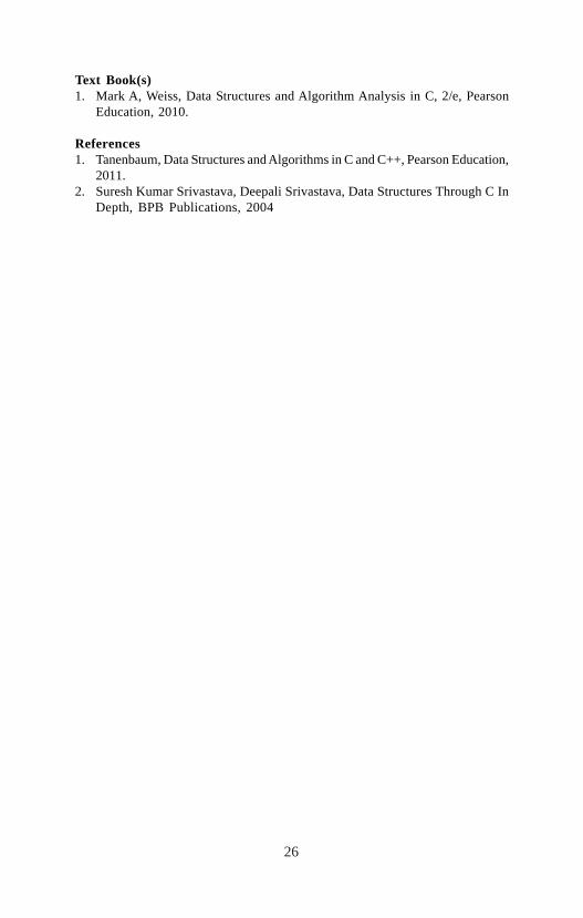
Text Book(s)1. Mark A, Weiss, Data Structures and Algorithm Analysis in C, 2/e, Pearson
Education, 2010.
References1. Tanenbaum, Data Structures and Algorithms in C and C++, Pearson Education,
2011.2. Suresh Kumar Srivastava, Deepali Srivastava, Data Structures Through C In
Depth, BPB Publications, 2004
27
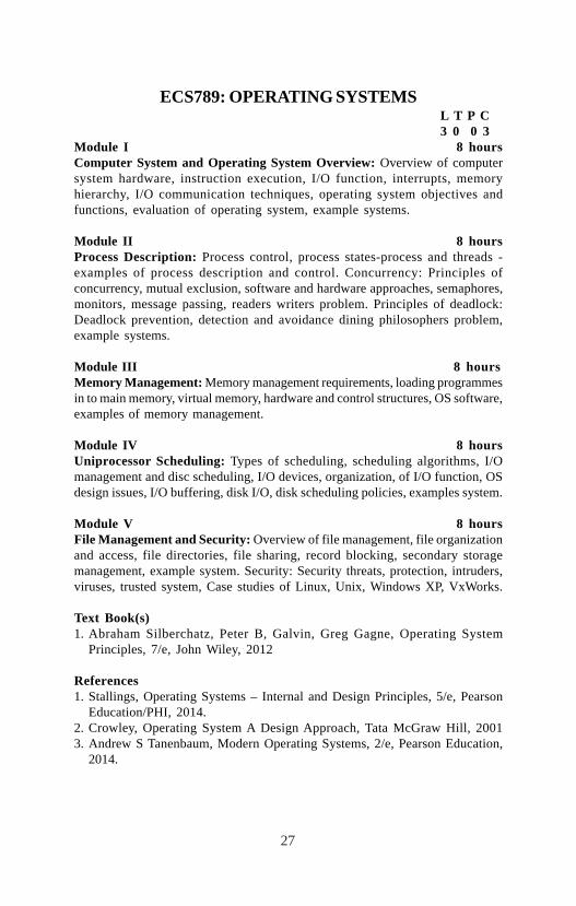
ECS789: OPERATING SYSTEMSL T P C3 0 0 3
Module I 8 hoursComputer System and Operating System Overview: Overview of computersystem hardware, instruction execution, I/O function, interrupts, memoryhierarchy, I/O communication techniques, operating system objectives andfunctions, evaluation of operating system, example systems.
Module II 8 hoursProcess Description: Process control, process states-process and threads -examples of process description and control. Concurrency: Principles ofconcurrency, mutual exclusion, software and hardware approaches, semaphores,monitors, message passing, readers writers problem. Principles of deadlock:Deadlock prevention, detection and avoidance dining philosophers problem,example systems.
Module III 8 hoursMemory Management: Memory management requirements, loading programmesin to main memory, virtual memory, hardware and control structures, OS software,examples of memory management.
Module IV 8 hoursUniprocessor Scheduling: Types of scheduling, scheduling algorithms, I/Omanagement and disc scheduling, I/O devices, organization, of I/O function, OSdesign issues, I/O buffering, disk I/O, disk scheduling policies, examples system.
Module V 8 hoursFile Management and Security: Overview of file management, file organizationand access, file directories, file sharing, record blocking, secondary storagemanagement, example system. Security: Security threats, protection, intruders,viruses, trusted system, Case studies of Linux, Unix, Windows XP, VxWorks.
Text Book(s)1. Abraham Silberchatz, Peter B, Galvin, Greg Gagne, Operating System
Principles, 7/e, John Wiley, 2012
References1. Stallings, Operating Systems – Internal and Design Principles, 5/e, Pearson
Education/PHI, 2014.2. Crowley, Operating System A Design Approach, Tata McGraw Hill, 20013. Andrew S Tanenbaum, Modern Operating Systems, 2/e, Pearson Education,
2014.
28
EEI780: CIRCUITS FOR ANALOG SYSTEM DESIGN
L T P C3 0 0 3
Module I 8 HoursTransistor as a switch, transistor as amplifier, problems in the transistor amplifier,temperature drift and device to device variation, 3-transistor op amp, use of op-amp for different applications and basic issues in use of op amps, designing alinear power supply using op amp, selection of components.
Module II 8 HoursDesign of heat sink and design of transformer for the linear power supply, designof low drop out regulators, design of temperature indicator using IC sensors,errors due to resistance drift, opamp offset voltage drift, offset current drift,error budgeting, design of an on/off temperature controller, design of differenttypes of heater drive circuits, thyristor and transistor based drive circuit design,error budgeting.
Module III 8 HoursDesign of proportional temperature controller circuit using thermocoupletemperature sensor, error budgeting, design of heater drive circuits using TRIACSand transistors, use of pulse width modulation circuits, use of MOSFETs andIGBTs, short circuit protection techniques.
Module IV 8 HoursDesign of PID temperature controllers, basics of PID parameter selection, designof constant current sources with error budgeting, design of 4-20ma currenttransmitter for resistance sensors, design of 4-20ma current transmitter for LVDTsensor, design of oscillator circuits, errors in the op amp circuit for ac amplifiers,errors in ac application.
Module V 8 HoursUse of instrumentation amplifier and its basis, designing of a capacitormeasurement circuit, ratio transformer technique, differential capacitormeasurement, errors in the capacitance measurement, phase sensitive detectionand use of the same for lock-in amplifier design, ADC/DAC converter types,use of ratio metric converters, error budgeting for the different types of ADC/DAC, band gap zenors and other reference diodes.
Text Book(s)1. Franco S, Design with Operational Amplifiers and Analog Integrated Circuits,
3/e, McGraw Hill, 2010.2. Paul Horowitz & Winfield Hill, The Art of Electronics, 2/e, Cambridge
University Press, 2011.
29
ECS782: COMPUTER ARITHMETICL T P C3 0 0 3
Module I 8 HoursNumber Representation: Numbers and arithmetic,what is computer arithmetic?,motivating examples, numbers and their encodings, fixed-radix positional numbersystems, number radix conversion, classes of number representations.Representing signed numbers: signed-magnitude representation, biasedrepresentations, complement representations, two's and 1's-complement numbers,direct and indirect signed arithmetic, using signed positions or signed digits.Redundant number systems: coping with the carry problem, redundancy incomputer arithmetic, digit sets and digit-set conversions, generalized signed-digitnumbers, carry-free addition algorithms, conversions and support functions.
Module II 8 HoursAddition / Subtraction: Basic addition and counting, bit-serial and ripple-carryadders, conditions and exceptions, analysis of carry propagation, carry completiondetection, addition of a constant, counters, manchester carry chains and adders.Carry-lookahead adders: unrolling the carry recurrence, carry-lookahead adderdesign, ling adder and related designs, carry determination as prefix computation,alternative parallel prefix networks, VLSI implementation aspects. Variations infast adders: simple carry-skip adder multilevel carry-skip adders, carry-selectadders, conditional-sum adder, hybrid designs and optimizations, modular two-operand adders.
Module III 8 HoursMultiplication: Shift/add multiplication algorithms, programmed multiplication,basic hardware multipliers, multiplication of signed numbers, multiplication byconstants, preview of fast multipliers. High-radix multipliers: radix-4multiplication, modified booth's recoding, using carry-save adders, radix-8 andradix-16 multipliers, multibeat multipliers, VLSI complexity issues. Tree and arraymultipliers: full-tree multipliers, alternative reduction trees, tree multipliers forsigned numbers, partial-tree and truncated multipliers, array multipliers, pipelinedtree and array multipliers.
Module IV 8 HoursDivision: Basic Division Schemes: Shift/subtract division algorithms, programmeddivision, restoring hardware dividers, non-restoring and signed division, divisionby constants, radix-2 SRT division. High-radix dividers: Basics of high-radixdivision, using carry-save adders, radix-4 SRT division, general high-radix dividers,quotient-digit selection, using p-d plots in practice. Variations in dividers: divisionwith prescaling, overlapped quotient-digit selection, combinational and arraydividers, modular dividers and reducers, the special case of reciprocation, combinedmultiply/divide units.

30
Module V 8 HoursReal Arithmetic: Floating-point representations, the ANSI/IEEE floating-pointstandard, basic floating-point algorithms, conversions and exceptions, roundingschemes, logarithmic number systems. Floating-Point Operations: Floating-pointadders/subtractors, pre- and postshifting, rounding and exceptions, floating-pointmultipliers and dividers, fused-multiply-add units, logarithmic arithmetic unit.
Text Book(s)1. B. Parhami, Computer Arithmetic: Algorithms and Hardware Designs, 2/e,
Oxford University Press, New York, 2010.
References1. Israel Koren, Computer Arithmetic Algorithms, 2/e, Prentice Hall Publications,
2011.2. Milos D.Ercegovac, Digital Arithmetic, The Morgan Kaufmann Series, 2012.

31
EEI762: MODERN DIGITAL SIGNAL PROCESSINGL T P C3 0 0 3
Module I 10 HoursMultirate Digital Signal Processing – Introduction, decimation by a factorD, interpolation by a factor I, sampling rate conversion by a rational factor I/D, implementation of sampling rate conversion, multistage implementation ofsampling rate conversion, applications of sampling rate conversion, digital filterbanks two-channel quadrature mirror filter bank.
Module II 10 HoursLinear Prediction And Optimum Linear Filters - Random signals, correlationfunctions and power spectra, innovations representation of a stationary randomprocess, forward and backward linear prediction, solution of the normal equationswiener filters for filtering and prediction.
Module III 10 HoursAdaptive Filters: Applications of adaptive filters, adaptive direct-form FIRfilters-the LMS algorithm, adaptive direct-form FIR filters-RLS algorithms.
Module IV 10 HoursPower Spectrum Estimation – Basic Methods Estimation of spectra from finite-duration observations of signals, nonparametric methods for power spectrumestimation, parametric methods for power spectrum estimation.
Module V 10 HoursPower Spectrum Estimation – Advanced Methods: Filter bank methods,Capon’s method, Eigen analysis algorithms for spectrum estimation, Pisarenkoharmonic decomposition method, MUSIC algorithm, ESPIRIT algorithm.
Text Book1. Proakis J. Gard & D. G. Manolakis, Digital Signal Processing: Principles,
Algorithms and Applications, 4/e, PHI, 2012.
References1. Monson Hayes, Statistical Digital Signal Processing, Wiley Student Edition,
2012.2. Manolakis, Vijay Ingle, Statistical and Adaptive Signal Processing, Artech Book
House, 2009.3. P. P. Vaidyanathan, Multirate systems and Filter banks, Prentice Hall, 2010.
32
ECS784: COMPUTER ARCHITECTUREL T P C3 0 0 3
Module I 8 HoursFundamentals of Computer Design: Technology trends, cost Measuring andreporting, performance quantitative principles of computer design. Instructionset principles and examples: Classifying instruction set, memory addressing, typeand size of operands, addressing modes for signal processing, operations in theinstruction set, instruction for control, encoding an instruction set.
Module II 8 HoursPipelining: Introduction, the major hurdle of pipelining-pipeline hazards, howis pipelining implemented?, what makes pipelining hard to implement?, extendingthe MIPS pipeline to handle multicycle operations. Instruction Level Parallelism:Overcoming hazards, reducing branch costs, high performance instruction delivery,hardware based speculation, limitation of ILP, ILP software approach, compilertechniques, static branch protection, VLIW approach.
Module III 8 HoursMemory Hierarchy Design: Introduction, review of the abcs of caches, cacheperformance, reducing cache miss penalty, reducing miss rate, reducing cachemiss penalty or miss rate via parallelism, reducing hit time, main memory andorganizations for improving performance, memory technology, virtual memory,protection and examples of virtual memory, basics of virtual machines.
Module IV 8 HoursMultiprocessors and Thread-Level Parallelism: Introduction, characteristicsof application domains, symmetric shared-memory architectures, performanceof symmetric shared-memory multiprocessors, distributed shared-memoryarchitectures, performance of distributed shared-memory multiprocessors,synchronization. Models of memory consistency: an introduction, multithreading,exploiting thread-level parallelism within a processor.
Module V 8 HoursStorage Systems: Introduction, types of storage devices, buses-connectingI/O devices to CPU/memory, reliability, availability, and dependability, RAID,redundant arrays of inexpensive disks, errors and failures in real systems, I/Operformance measures, designing an I/O system in five easy pieces.Text Book(s)1. John L, Hennessy & David A Patterson, Computer Architecture a quantitative
approach, 3/e, Morgan Kuffman, 2011.References1. John L, Hennessy & David A Patterson, Computer Architecture a quantitative
approach, 4/e, Morgan Kuffman, 2012.2. Kai Hwang and A. Briggs, Computer Architecture and Parallel Processing,
International Edition, McGraw Hill, 2011.3. DezsoSima, Terence Fountain, Peter Kacsuk, Advanced Computer
Architecture, Pearson Education, 2011.

33
EEC753: EMBEDDED SYSTEM DESIGNL T P C3 0 0 3
Module I 8 HoursIntroduction: Features of embedded systems, design metrics, embedded systemdesign flow, ARM microcontroller, structure of ARM7, ARM pipeline,instruction set architecture, thumb instructions, exceptions in ARM, programmingexamples.
Module II 8 HoursDigital Signal Processors: Architecture of digital signal processors, high speeddata access, fast computation, higher accuracy, C6000 family of DSPs. Fieldprogrammable gate arrays: Field programmable devices, programmability ofFPGAs, FPGA logic block variations, FPGA design flow, modern FPGAs.
Module III 8 HoursInterfacing: Serial peripheral interface (SPI), inter integrated circuit (IIC),RS232c, RS422, RS485, universal serial bus, infrared communication, controllerarea network, bluetooth.
Module IV 8 HoursReal-Time Operating System: Type of real-time tasks, task periodicity, taskscheduling, classification of scheduling algorithms, clock driven scheduling, eventdriven scheduling, resource sharing, features of RTOS, commercial RTOS.
Module V 8 HoursSpecification Techniques: State chart, specification description language (SDL),petri nets, unified modeling language. Hardware software co-simulation:dimensions in co-simulation, co-simulation approaches, typical co-simulationenvironment.
Text Book(s)1. Santanu Chattopadhyay, Embedded System Design, 2/e, Prentice Hall of India,
2013
References1. David Simon, An Embedded Software Primer, Pearson Education, India, 20072. Arnold S Burger, Embedded System design, Taylor and Francis, 2002.3. Steve Heath, Embedded Systems Design: Real world design Newton Mass
USA 2002.

34
EEI782 : ARM SYSTEM DEVELOPMENT
L T P C3 0 0 3
Module I 8 HoursARM Introduction and Pipeline structures: Types of computer architectures,ISA's and ARM History. Embedded System Software and Hardware, stackimplementation in ARM, endianness, condition codes. Processor core VS CPUcore, ARM7TDMI Interface signals, Memory Interface, Bus Cycle types, Registerset, Operational Modes. Instruction Format, ARM Core Data Flow Model, ARM3 stage Pipeline, ARM family attribute comparison. ARM 5 stage Pipeline,Pipeline Hazards, Data forwarding - a hardware solution.
Module II 8 HoursARM7TDMI assembly instructions and modes: ARM ISA and ProcessorVariants, Different Types of Instructions, ARM Instruction set, data processinginstructions. Shift Operations, shift Operations using RS lower byte, Immediatevalue encoding. Dataprocessing Instructions.AddressingMode-1, Addressing Mode-2. Addressing Mode -2, LDR/STR, Addressing mode -3 with examples.Instruction Timing, Addressing Mode - 4 with Examples. Swap Instructions, SwapRegister related Instructions, Loading Constants. Program Control Flow, ControlFlow Instructions, B & BL instructions, BX instruction.Interrupts andExceptions, Exception Handlers, Reset Handling.Aborts, software InterruptInstruction, undefined instruction exception. Interrupt Latency, MultiplyInstructions, Instruction set examples. Thumb state, Thumb Programmers model,Thumb Implementation, Thumb Applications. Thumb Instructions, Interruptprocessing. Interrupt Handelling schemes, Examples of Interrupt Handlers.
Module III 8 HoursARM Coprocessor Interface and VFP: ARM coprocessor interface andInstructions, Coprocessor Instructions, data Processign Instruction, data transfers,register transfers. Number representations, floating point representation(IEEE754). Flynn's Taxonomy, SIMD and Vector Processors, Vector FloatingPoint Processor (VFP), VFP and ARM interactions, An example vector operation.
Module IV 8 HoursCache and Memory Management and Protection: Memory Technologies,Need for memory Hierarchy, Hierarchical Memory Organization, Virtual Memory.Cache Memory, Mapping Functions. Cache Design, Unified or split cache,multiple level of caches, ARM cache features, coprocessor 15 for system control.Processes, Memory Map, Protected Systems, ARM systems with MPU, memoryProtection Unit (MPU). Physical Vs Virtual Memory, Paging, Segmentation.MMU Advantage, virtual memory translation, Multitasking with MMU, MMUorganization, Tightly coupled Memory (TCM).
35
Module V 8 HoursARM tools and Peripherals: ARM Development Environment, Arm ProcedureCall Standard (APCS), Example C program. Embedded software Development,Image structure, linker inputs and outputs, memory map, application startup.AMBA Overview, Typical AMAB Based Microcontroller, AHB bus features,AHB Bus transfers, APB bus transfers, APB bridge. DMA, Peripherals,Programming Peripherals in ARM. ARM ISAs, ARMv5, ARMv6, ARM v7,big.little technology, ARMv8. ARM ISAs, ARMv5, ARMv6, ARM v7, big.littletechnology, ARMv8.
References1. Andrew N. Sloss, Dominic Symes, Chris Wright, ARM System Developers
Guide, Elsevier, 2004.2. Steve Furber, ARM System on Chip Architecture, 2/e, Pearson Education,
2013.3. William Stallings, Operating Systems, 5/e, Pearson Education, 2014.4. Manuals and Technical Documents from the ARM Inc. Website5. Http://nptel.ac.in/courses/117106111

36
EEC740: SEMICONDUCTOR DEVICESL T P C3 1 0 4
Module I 10 HoursReview of Electronics in Solids. Electronics in Semiconductors: Introduction,band structure of semiconductors, holes in semiconductors, band structures ofsome semiconductors, mobile carriers, doping, carriers in doped semiconductors.Carrier Dynamics in Semiconductors: Introduction, scattering in semiconductors,velocity electric field relations in semiconductors, very high field transport, carriertransport by diffusion, charge injection and quasi Fermi levels, carrier generationand recombination, continuity equation.
Module II 10 HoursJunctions in Semiconductors: Device demands, unbiased p-n junction, p-njunction under bias, real diode, high voltage effects in diodes, modulation andswitching AC response. SPICE model. Semiconductor Junctions with metal andinsulators: Metals as conductors, Schottky barrier diode, ohmic contacts, insulator-semiconductor junctions.
Module III 10 HoursBipolar Junction Transistors: Introduction, bipolar transistor, staticcharacteristics of bipolar transistors, BJT static performance parameters,secondary effects in real devices, a charge control analysis, bipolar transistoras an inverter, high frequency behavior of BJT. Spice model. Bipolar transistors:A Technology roadmap.
Module IV 10 HoursField Effect Transistors(MOSFET): Introduction, MOSFET, structure andfabrication, metal-oxide semiconductor capacitor, capacitance voltagecharacteristics of the MOS structure, metal oxide semiconductor field effecttransistor, important issues in real MOSFETs,
Module V 10 HoursField Effect Transistors (JFET, MESFET): Introduction, JFET, MESFET,current voltage characteristics, effects in real devices, high frequency high speedissues. Semiconductor Optoelectronics: Introduction, optical absorption in asemiconductor, photo current in a p-n diode, P-I-N photodetector, light emission,semiconductor laser-basic principles.Text Book(s)1. Jasprit Singh, Semiconductor Devices, Basic Principles, Wiley Student
Edition, 20122. Ben G. Streetman, Solid State Electronic Devices, 6/e, Prentice Hall India, 2013.References1. Yuan Taur, Tak.H.Ning, Fundamentals of Modern VLSI Devices, 2/e,
Cambridge University Press, 2011.2. Donald Neamen, Semiconductors Physics and Devices, 3/e, Tata McGraw Hill,
2011.3. Tyagi, Introduction to Semiconductor Materials and Devices, Wiley
Publications, 2010.

37
EEC741: ACTIVE FILTER DESIGNL T P C3 1 0 4
Module I 10 HoursOperational Amplifiers: Operational amplifier models, opamp slew rate,operational amplifier with resistive feedback, analyzing opamp circuits, examples.First Order Filters: Bilinear transfer function and its parts, realization with passiveelements, bode plots, active realizations, effect of A(s), cascade design.
Module II 10 HoursSecond Order LowPass and BandPass Filters: Design parameters Q and w0,second order circuit, frequency response of lowpass and bandpass circuits,integrators, other biquads. Second Order Filters with Arbitrary transmissionzeros: Summing, voltage feedforward, cascade design revisited.
Module III 10 HoursLow Pass filters with Maximally Flat Magnitude: Ideal low pass filter,Butterworth response, Butterworth pole locations, low pass filter specifications,arbitrary transmission zeros. Low Pass filters with Equal Ripple MagnitudeResponse: The Chebyshev polynomial, Chebyshev magnitude response, localof Chebyshev poles, comparision of maximally flat and equal ripple responses,Chebyshev filter design. Frequency Transformation: Low pass to highpass, lowpass to bandpass, low pass to bandstop, lowpass to multiple passbandtransformation.
Module IV 10 HoursLC Ladder Filters: Some properties of lossless ladders, a synthesis strategy,General ladder design methods, frequency transformation, design of passiveequalizers. Ladder Simulations by Element Replacement: The general impedanceconverter, optimal design of the GIC, realizing simple ladders, Gorski-Popielembedding technique, bruton’sfdnr technique, creating negative components
Module V 10 HoursTransconductance-C filters: Transconductance cells, elementarytransconductance building blocks, first order and second order filters, higher orderfilters. Switched Capacitor Filters: The MOS Switch, the switched capacitor,first order building blocks, second order sections, sampled data operation, switchedcapacitor first order and second order sections, bilinear transformation, designof switched capacitor cascade filters.Text Book(s)1. Rolf Schaumann, Van Valkenburg, Design of Analog Filters, Oxford University
Press, 2010References1. YannisTsividis and Johannes Voorman, Integrated Continuous Time Filters,
IEEE Press, 2011.2. Rolf Schaumann, M.S. Ghausi, Kenneth R. Laker, Oxford University Press,
Design of Analog Filters: Passive, Active RC and Switched Capacitor, 2010
38
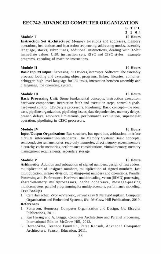
EEC742: ADVANCED COMPUTER ORGANIZATIONL T P C3 1 0 4
Module I 10 HoursInstruction Set Architecture: Memory locations and addresses, memoryoperations, instructions and instruction sequencing, addressing modes, assemblylanguage, stacks, subroutines, additional instructions, dealing with 32-bitimmediate values, CISC instruction sets, RISC and CISC styles, exampleprograms, encoding of machine instructions.
Module II 10 HoursBasic Input/Output: Accessing I/O Devices, interrupts. Software: The assemblyprocess, loading and executing object programs, linker, libraries, compiler,debugger, high level language for I/O tasks, interaction between assembly andc language, the operating system.
Module III 10 HoursBasic Processing Unit: Some fundamental concepts, instruction execution,hardware components, instruction fetch and execution steps, control signals,hardwired control, CISC-style processors. Pipelining: Basic concept—the idealcase, pipeline organization, pipelining issues, data dependencies, memory delays,branch delays, resource limitations, performance evaluation, superscalaroperation, pipelining in CISC processors.
Module IV 10 HoursInput/Output Organization: Bus structure, bus operation, arbitration, interfacecircuits, interconnection standards. The Memory System: Basic concepts,semiconductor ram memories, read-only memories, direct memory access, memoryhierarchy, cache memories, performance considerations, virtual memory, memorymanagement requirements, secondary storage.
Module V 10 HoursArithmetic: Addition and subtraction of signed numbers, design of fast adders,multiplication of unsigned numbers, multiplication of signed numbers, fastmultiplication, integer division, floating-point numbers and operations. ParallelProcessing and Performance: Hardware multithreading, vector (SIMD) processing,shared-memory multiprocessors, cache coherence, message-passingmulticomputers, parallel programming for multiprocessors, performance modeling.Text Book(s)1. Carl Hamacher, ZvonkoVranesic, Safwat Zaky & NaraigManjikian, Computer
Organization and Embedded Systems, 6/e, McGraw Hill Publications, 2010.References1. Patterson, Hennessy, Computer Organization and Design, 4/e, Elsevier
Publications, 2011.2. Kai Hwang and A. Briggs, Computer Architecture and Parallel Processing,
International Edition McGraw Hill, 2012.3. DezsoSima, Terence Fountain, Peter Kacsuk, Advanced Computer
Architecture, Pearson Education, 2011.

39
EEC743: ADVANCED DIGITAL IC DESIGN
L T P C3 1 0 4
Module I 10 HoursImplementation Strategies for Digital ICs: Introduction, from custom tosemicustom and structured array design approaches, custom circuit design, cell-based design methodology, standard cell, compiled cells, macrocells, megacellsand intellectual property, semi-custom design flow, array-based implementationapproaches, pre-diffused (or mask-programmable) arrays, pre-wired arrays,perspective the implementation platform of the future.
Module II 10 HoursThe Wire: Introduction, a first glance, interconnect parameters—capacitance,resistance, and inductance, electrical wire models, SPICE wire models. Copingwith interconnect: introduction, capacitive parasitics, capacitance and reliability-cross talk, capacitance and performance in CMOS, resistive parasitics, resistanceand reliability-ohmic voltage drop, electromigration, resistance and performance—RC delay.
Module III 10 HoursTiming Issues in Digital Circuits: Introduction, timing classification of digitalsystems, synchronous interconnect, mesochronous interconnect, plesiochronousinterconnect, asynchronous interconnect, synchronous design an in-depthperspective, synchronous timing basics, sources of skew and jitter, clock-distribution techniques, synchronizers and arbiters, synchronizers—concept andimplementation, arbiters, clock synthesis and synchronization using a phase-locked loop, basic concept, building blocks of a PLL.
Module IV 10 HoursDesigning Arithmetic Building Blocks: Introduction, datapaths in digitalprocessor architectures, the adder, the binary adder, definitions, the full adder,circuit design considerations, the binary adder, logic design considerations, themultiplier, the multiplier, definitions, partial-product generation, partial productaccumulation, final addition, multiplier summary, the shifter, barrel shifter,logarithmic shifter.
Module V 10 HoursDesigning Memory and Array Structures: Introduction, memory classification,memory architectures and building blocks, the memory core, read-only memories,nonvolatile read-write memories, read-write memories (RAM), contents-addressable or associative memory (CAM), memory peripheral circuitry, theaddress decoders, sense amplifiers, voltage references, drivers/buffers, timing andcontrol.
40
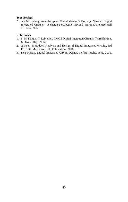
Text Book(s)2. Jan M. Rabaey, Anantha space Chandrakasan & Borivoje Nikolic, Digital
Integrated Circuits – A design perspective, Second Edition, Prentice Hallof India, 2012.
References1. S. M. Kang & Y. Leblebici, CMOS Digital Integrated Circuits, Third Edition,
McGraw Hill, 2012.2. Jackson & Hodges, Analysis and Design of Digital Integrated circuits, 3rd
Ed, Tata Mc Graw Hill, Publication, 2010.3. Ken Martin, Digital Integrated Circuit Design, Oxford Publications, 2011.

41
EEC747: BROADBAND COMMUNICATION CIRCUITSL T P C3 1 0 4
Module I 10 HoursIntroduction: Introduction to broadband digital communication, serializers anddeserializers, power and delay in CMOS and current driven logic circuits, CMOSlogic, single ended data transmission, limitations, current mode logic-basic circuitdesign, current mode logic-MUX, XOR, latch, current mode logic-latch design,current mode logic-latch characteristics
Module II 10 HoursLow pass transmission channel-Intersymbol interference, error rate, First orderchannel model, ISI, Jitter, eye opening, channel characteristics-intersymbolinterference, crosstalk, equalizer design, equalizer design-minimizing the residualerror, equalization-effect on noise and crosstalk, tradeoffs between equalizationat Tx and Rx; design of Tx equalizers.
Module III 10 HoursDesign of Transmit Equalizers: Design of transmit equalizers using flip-flopsand transconductors, Tx equalizer-design considerations; realizing variablecoefficients, differential pair-effect of tail node capacitance, continuous timeequalization, continuous-time equalizer realization, replica biasing for the tailcurrent source, replica biasing, optimizing transmitter swing, replica biasing,optimizing transmitter swing, analog layout optimization.
Module-IV 10 HoursDesign of Receiver Equalizers: Equalization at the receiver; basics of adaptation,LMS adaptation, sign-sign LMS adaptation, LMS implementation details,adaptive equalizer implementation, S/H based equalizer, obtaining the gradients,multiplexed and demultiplexed PRBS sequences, latch vs. amplifier, zeros forpre- and post- cursor equalization, echo cancellation, decision feedback equalizers-elimination of noise enhancement, error propagation, BER analysis,implementation issues.
Module V 10 HoursClock and Data Recovery: Frequency multiplication using a phase locked loop,Type I PLL; derivation of the phase model of the PLL, Tri state phase detector,reference feedthrough, tradeoff between reference feedthrough and lock range,stability of feedback loops; derivation of the type II PLL, realization of typeII PLLs-charge pump, loop filter, reference feedthrough in a type II PLL; phasedetector for random data, linear phase detector for random data, transfer functionsin a PLL, binary phase detectors; bang bang jitter, optimal equalizers, linearityassumption of PLL model, PLL capture phenomenon, Hogge phase detector offsetcorrection.

42
Text Book(s)1. Behzad Razavi, Monolithic Phase Locked Loops and Clock Recovery
Circuits-Theory and Design, IEEE Press, 1996.2. Behzad Razavi, Phase Locking in High Performance Systems-From Devices
to Architectures, IEEE Press, 2003.3. Behzad Razavi, Design of Integrated Circuits for Optical Communications,
McGraw-Hill, 2002.
References1. William J, Dally, John W, Poulton, Digital Systems Engineering, Cambridge
University Press, 1998,2. IEEE Journal of Solid State Circuits, IEEE, http://ieeexplore,ieee,org3. http://www.ee.iitm.ac.in/videolectures/doku.php? id =ee685:start
43
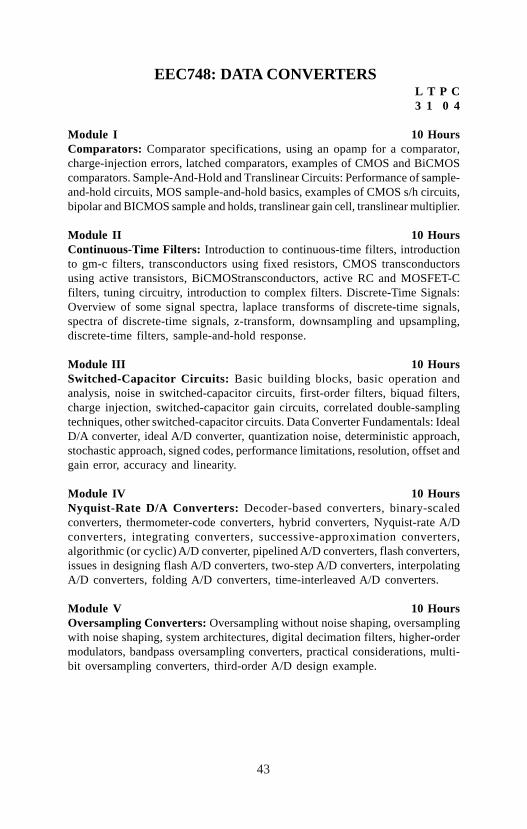
EEC748: DATA CONVERTERSL T P C3 1 0 4
Module I 10 HoursComparators: Comparator specifications, using an opamp for a comparator,charge-injection errors, latched comparators, examples of CMOS and BiCMOScomparators. Sample-And-Hold and Translinear Circuits: Performance of sample-and-hold circuits, MOS sample-and-hold basics, examples of CMOS s/h circuits,bipolar and BICMOS sample and holds, translinear gain cell, translinear multiplier.
Module II 10 HoursContinuous-Time Filters: Introduction to continuous-time filters, introductionto gm-c filters, transconductors using fixed resistors, CMOS transconductorsusing active transistors, BiCMOStransconductors, active RC and MOSFET-Cfilters, tuning circuitry, introduction to complex filters. Discrete-Time Signals:Overview of some signal spectra, laplace transforms of discrete-time signals,spectra of discrete-time signals, z-transform, downsampling and upsampling,discrete-time filters, sample-and-hold response.
Module III 10 HoursSwitched-Capacitor Circuits: Basic building blocks, basic operation andanalysis, noise in switched-capacitor circuits, first-order filters, biquad filters,charge injection, switched-capacitor gain circuits, correlated double-samplingtechniques, other switched-capacitor circuits. Data Converter Fundamentals: IdealD/A converter, ideal A/D converter, quantization noise, deterministic approach,stochastic approach, signed codes, performance limitations, resolution, offset andgain error, accuracy and linearity.
Module IV 10 HoursNyquist-Rate D/A Converters: Decoder-based converters, binary-scaledconverters, thermometer-code converters, hybrid converters, Nyquist-rate A/Dconverters, integrating converters, successive-approximation converters,algorithmic (or cyclic) A/D converter, pipelined A/D converters, flash converters,issues in designing flash A/D converters, two-step A/D converters, interpolatingA/D converters, folding A/D converters, time-interleaved A/D converters.
Module V 10 HoursOversampling Converters: Oversampling without noise shaping, oversamplingwith noise shaping, system architectures, digital decimation filters, higher-ordermodulators, bandpass oversampling converters, practical considerations, multi-bit oversampling converters, third-order A/D design example.

44
Text Book(s)1. Tony Chan Carusone, Kenneth W, Martin, David A, Johns, Analog
Integrated Circuit Design, 2nd Edition, Wiley Publications 2011,2. Allen Holberg, CMOS Analog Circuit Design, 2/e, Oxford Publications, 2012
References1. M. Gustavsson, J, Wikner, and N, Tan, CMOS Data Converters for
Communication - Kluwer Academic Publishers, 2009.2. Behzad Razavi, Principles of Data Conversion System Design, IEEE Press,
2010.3. Baker Li, Boyce, CMOS Mixed Signal Design, Wiley Publications, 2011.

45
EEC750: DIGITAL SIGNAL PROCESSING WITH FPGAs
L T P C 3 1 0 4
Module I 10 HoursIntroduction: Overview of digital signal processing, FPGA technology, DSPtechnology requirements, FPGA and programmable signal processors. ComputerArithmetic: Number representation, fixed-point numbers, unconventional fixed-point numbers, floating-point numbers, binary adders, pipelined adders, moduloadders, binary multipliers, multiplier blocks, binary dividers, fixed-pointarithmetic implementation, floating-point arithmetic implementation.
Module II 10 HoursFIR Filters: Digital filters, FIR theory, designing FIR filters, constant coefficientFIR design. IIR Filters: IIR coefficient computation, IIR filter implementation,Fast IIR filter.
Module III 10 HoursMultirate Signal Processing: Decimation and interpolation, polyphasedecomposition, Hoegenaur CIC filters, filter banks. Fourier Transforms: DFTalgorithms, FFT algorithms, computing DCT using FFT.
Module IV 10 HoursAdaptive Systems: Application of adaptive systems, optimum estimationtechniques, LMS algorithm, transform domain LMS algorithms, implementationof the LMS algorithm.
Module V 10 HoursCommunication Systems: Error control, basic concepts from coding theory,block codes, convolutional codes, modulation and demodulation.
Text Book(s)1. Uwe Meyer-Baese, Digital Signal Processing with Field Programmable Gate
Arrays, Fourth Edition, Springer Publications, 2014
References1. Roger Woods, John McAllister, Dr. Ying Yi, FPGA-based Implementation
of Signal Processing Systems, Wiley Publications, 2011.2. Shoab Ahmed Khan, Digital Design of Signal Processing Systems, Wiley
Publications, 2011.3. Keshab Parhi, VLSI Digital Signal Processing, Wiley Student Edition, 2010.

46
EEC713: DSP PROCESSORS AND ARCHITECTURESL T P C
3 1 0 4Module I 10 HoursReview of Digital Signal Processing: The sampling process, discrete timesequences, discrete Fourier transform and FFT, linear time–invariant systems,digital filters, decimation and interpolation, analysis and design tool for DSPsystems. Computational accuracy in DSP Implementations: Number formatsfor signals and coefficients in DSP systems, dynamic range and precision, sourcesof error in DSP implementations, A/D conversion errors, DSP computationalerrors, D/A conversion errors, compensating filter.
Module II 10 HoursArchitectures for Programmable DSP Devices: Basic architectural features,DSP computational building blocks, bus architecture and memory, data addressingcapabilities, address generation unit, programmability and program execution,speed issues, features for external interfacing. Programmable Digital SignalProcessors: Introduction, commercial digital signal processing devices, thearchitecture of TMS320c54xx digital signal processors, addressing modes of theTMS320c54xx processors, memory spaces of TMS320c54xx processors, programcontrol, TMS320c54xx instructions and programming, on-chip peripherals.Interrupts, pipeline operation of the TMS320c54xx processors.
Module III 10 HoursImplementation of Basic DSP Algorithms: Introduction, the Q-notation, FIRfilters, IIR filters, interpolation filters, decimation filters, PID controller, adaptivefilters, 2-D signal processing. Implementation of FFT Algorithms: Introduction,an FFT algorithm for DFT computation, a butterfly computation, overflow andscaling, bit-reversed index generation, an 8-point FFT implementation ofTMS320c54xx, computation of signal spectrum.
Module IV 10 HoursInterfacing Memory and Parallel IO Peripherals to Programmable DSPDevices: Introduction, memory space organization of the TMS320C54xx devices,memory and I/O signals of the TMS320C54xx devices, memory interface, parallelI/O, programmed I/O, interrupts and I/O, direct memory access (DMA).
Module V 10 HoursInterfacing Serial Converters to a Programmable DSP Device: Introduction,synchronous serial interface between the DSP and an AIC, a multi-channelbuffered serial port (McBSP), the McBSP programming, a CODEC interfacecircuit, CODEC programming, a CODEC-DSP interface example. Applications:Introduction, a DSP system, DSP based biotelemetry system, a speech processingsystem, an image processing system, a position control system for a hard diskdrive, DSP based power meter.

47
Text Book(s)1. Avtar Singh and S. Srinivasan, Digital Signal Processing, Cengage Learning,
India, 2012.
References1. Rulph Chassaing, Digital Signal Processing with C6713 and C6416 DSK,
2/e Wiley Publications, 2013.2. Lapsley et al. DSP processor fundamentals, Architecture & Features- S. Chand
& Co, 2012.3. Steve Tretter, Communication System Design using DSP Algorithms, Springer
Publications, 2011
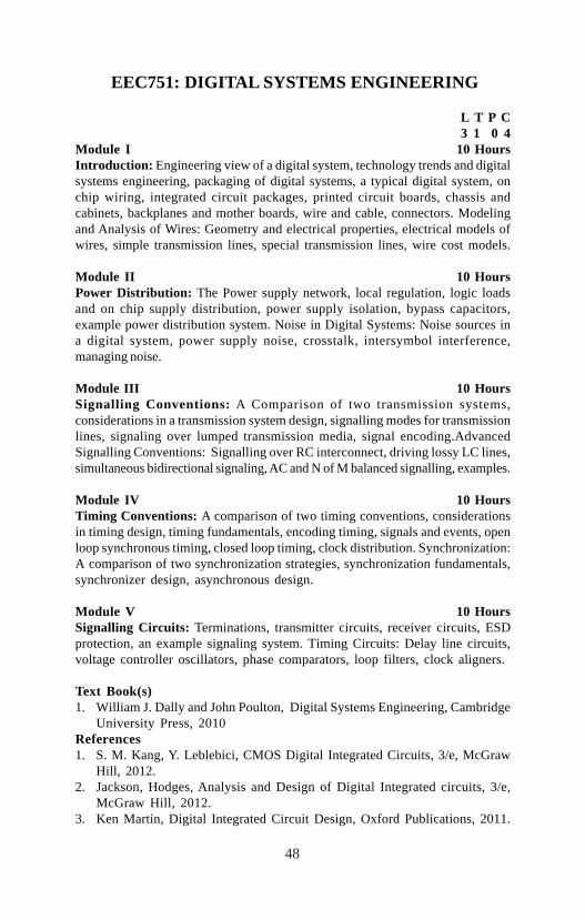
48
EEC751: DIGITAL SYSTEMS ENGINEERING
L T P C3 1 0 4
Module I 10 HoursIntroduction: Engineering view of a digital system, technology trends and digitalsystems engineering, packaging of digital systems, a typical digital system, onchip wiring, integrated circuit packages, printed circuit boards, chassis andcabinets, backplanes and mother boards, wire and cable, connectors. Modelingand Analysis of Wires: Geometry and electrical properties, electrical models ofwires, simple transmission lines, special transmission lines, wire cost models.
Module II 10 HoursPower Distribution: The Power supply network, local regulation, logic loadsand on chip supply distribution, power supply isolation, bypass capacitors,example power distribution system. Noise in Digital Systems: Noise sources ina digital system, power supply noise, crosstalk, intersymbol interference,managing noise.
Module III 10 HoursSignalling Conventions: A Comparison of two transmission systems,considerations in a transmission system design, signalling modes for transmissionlines, signaling over lumped transmission media, signal encoding.AdvancedSignalling Conventions: Signalling over RC interconnect, driving lossy LC lines,simultaneous bidirectional signaling, AC and N of M balanced signalling, examples.
Module IV 10 HoursTiming Conventions: A comparison of two timing conventions, considerationsin timing design, timing fundamentals, encoding timing, signals and events, openloop synchronous timing, closed loop timing, clock distribution. Synchronization:A comparison of two synchronization strategies, synchronization fundamentals,synchronizer design, asynchronous design.
Module V 10 HoursSignalling Circuits: Terminations, transmitter circuits, receiver circuits, ESDprotection, an example signaling system. Timing Circuits: Delay line circuits,voltage controller oscillators, phase comparators, loop filters, clock aligners.
Text Book(s)1. William J. Dally and John Poulton, Digital Systems Engineering, Cambridge
University Press, 2010References1. S. M. Kang, Y. Leblebici, CMOS Digital Integrated Circuits, 3/e, McGraw
Hill, 2012.2. Jackson, Hodges, Analysis and Design of Digital Integrated circuits, 3/e,
McGraw Hill, 2012.3. Ken Martin, Digital Integrated Circuit Design, Oxford Publications, 2011.

49
EEC752: DIGITAL SYSTEMS TESTING AND TESTABILITY
L T P C3 1 0 4
Module I 10 HoursIntroduction: Introduction, testing philosophy, role of testing, digital and analogVLSI testing. VLSI Testing Process and Test Equipment: How to test chips.Test Economics and Product Quality: Test economics, yield. Fault Modeling:Defects, errors and functional versus structural testing, levels of fault models,glossary of fault models, single stuck-at fault. Logic And Fault Simulation:Simulation for design verification, simulation for test evaluation, modeling circuitsfor simulation, algorithms for true-value simulation, algorithms for fault simulation,statistical methods for fault simulation.
Module II 10 HoursCombinational Circuit Test Generation: Algorithms and representations,redundancy identification (RID), testing as a global problem, definitions,significant combinational ATPG algorithms.
Module III 10 HoursSequential Circuit Test Generation: ATPG for single-clock synchronouscircuits, time-frame expansion method, simulation-based sequential circuit ATPG.
Module IV 10 HoursMemory Test: Memory density and defect trends, faults, memory test levels,march test notation, fault modeling, memory testing Digital DFT and Scan Design:Ad-Hoc DFT methods, scan design, partial-scan design, variations of scan.
Module V 10 HoursBuilt-In Self Test: The economic case for BIST, random logic BIST, memoryBIST, delay fault BIST. Boundary Scan Standard: Motivation, systemconfiguration with boundary scan, boundary scan description language.
Text Book(s)1. M. L. Bushnel, V. D. Agarwal, Essentials of Testing for Digital, Memory
and Mixed-Signal VLSI Circuits, Kluwer Academic Publishers, 2012.
References1. M. Abramovici, M. A. Breuer, A. D. Friedman, Digital Systems Testing and
Testable Design, Piscataway, IEEE Press, 2011.2. NirajJha, Sandeep Gupta, Test of Digital Systems, Cambridge University
Press, 2010.3. Robert J. Feugate, Steven M. McIntyre, Introduction to VLSI Testing,
Prentice Hall Publications, 2010.
50
EEC761: LOGIC SYNTHESIS AND VERIFICATION
L T P C3 1 0 4
Module I 10 HoursBackground and Hardware Modeling: Graphs, combinatorial optimization,graph optimization problems and algorithms, Boolean algebra and its applications,Hardware Modeling:Introduction, hardware modeling languages, abstract models,compilation and behavioral optimization.
Module II 10 HoursTwo Level Combinational Logic Optimization: Introduction, logicoptimization techniques, operations on two level logic covers, algorithms for logicminimization, symbolic minimization and encoding problems.
Module III 10 HoursMultilevel Combinational Logic Optimization: Introduction, models andtransformations for combinational networks, the algebraic model, the Booleanmodel, synthesis of testable networks, algorithms for delay evaluation andoptimization, rule based systems for logic optimization.
Module IV 10 HoursSequential Logic Optimization: Introduction, sequential circuit optimizationusing state based models, sequential circuit optimization using network models,implicit finite state machine traversal methods, testability considerations forsynchronous circuits.
Module V 10 HoursCell Library Binding: Introduction, problem formulation and analysis, algorithmsfor library binding, specific problems and algorithms for library binding, rule basedlibrary binding.
Text Book(s)1. G. De Micheli, Synthesis and Optimization of Digital Circuits, McGraw-
Hill, 2012.
References1. G. D. Hachtel, F. Somenzi, Logic Synthesis and Verification Algorithms,
Kluwer Academic Publishers, 2011.
51
EEC762: LOW POWER VLSI DESIGN
L T P C3 1 0 4
Module I 10 HoursPhysics of Power Dissipation in CMOS FET Devices: Physics of powerdissipation in MOSFET devices, power dissipation in CMOS, low power VLSIdesign limits.
Module II 10 HoursPower Estimation: Modeling in signals, signal probability calculation,probabilistic techniques for signal activity estimation, statistical techniques,estimation of glitching power, sensitivity analysis,power estimation using theinput vector compaction, power dissipation in domino CMOS, high level powerestimation, information theory based approaches, estimation of maximum power.
Module III 10 HoursSynthesis for Low Power: Behavioural level transforms, logic level optimizationfor low power, circuit Level optimization. Design and Test of Low Voltage CMOSCircuits: Circuit design style, leakage current in deep submicrometer transistors,deep submicrometer device design issues, key to minimizing SCE, low voltagecircuit design techniques, designing deep submicrometer ICS with elevated intrinsicleakage, multiple supply voltages.
Module IV 10 HoursLow Power Static RAM Architectures: Organization of a static RAM, MOSstatic RAM memory cell, banked organization of SRAMs, reducing voltage swingson bit lines, reducing power in write driver circuits, reducing power in senseamplifier circuits, method for achieving low core voltages from a single supply.
Module V 10 HoursLow Energy Computing using Energy Recovery Techniques: Energydissipation in transistor channel using an RC model, energy recovery circuitdesign, designs with partially reversible logic, supply clock generation.
Text Book(s)1. Kaushik Roy, Sharat C. Prasad, Low Power CMOS VLSI Circuit Design,
John Wiley and Sons, 2012.2. Jan Rabaey, Low Power Design Essentials, Springer Publications, 2011.
References1. Chandrakasan, R, Brodersen, Low-Power CMOS Design, IEEE Press, 2011.2. Gary Yeap, Practical Low Power Digital VLSI Design, Springer Publications,
2012.3. S. Narendra, A. Chandrakasan, Leakage in Nanometer CMOS Technologies,
Springer, 2011.

52
EEC767: MODELING AND DESIGN WITH HDLsL T P C3 1 0 4
Module I 10 HoursBasic Concepts: Lexical conventions, data types, system tasks and compilerdirectives. Modules and Ports: Modules, ports, hierarchical names. Gate-LevelModeling: Gate types, gate delays.
Module II 10 HoursDataflow Modeling: Continuous assignments, delays, expressions, operators,and operands, operator types, examples.
Module II 10 HoursBehavioral Modeling: Structured procedures, procedural assignments, timingcontrols, conditional statements, multiway branching, loops, sequential andparallel blocks, generate blocks, examples.
Module III 10 HoursTasks and Functions: Difference between tasks and functions, tasks, functions.Procedural Continuous Assignments: Overriding parameters, conditionalcompilation and execution, time scales, useful system tasks.Timing and Delays:Types of delay models, path delay modeling, timing checks, delay back-annotation.
Module IV 10 HoursSwitch Level Modeling: Switching-modeling elements, examples. User-DefinedPrimitives: UDP basics, combinational UDPs, sequential UDPs, UDP tableshorthand symbols, guidelines for UDP design.
Module V 10 HoursWriting Testbenches: Basic testbenches, testbench structure, constrainedrandom stimulus generation, object-oriented programming, assertion-basedverification. System Verilog Simulation: Event-driven simulation, SystemVerilogsimulation races, delay models, Simulator tools. System Verilog Synthesis: RTLsynthesis: Non-synthesizable SystemVerilog, Constraints, attributes, area andstructural constraints synthesis for FPGAs, behavioral synthesis, verifyingsynthesis results
Text Book(s)1. Samir Palnitkar, Verilog HDL, 2/e, Pearson Education, 2013.2. Mark Zowilski, Digital System Design with System Verilog, Pearson
Education., 2010.
References1. J. Bhasker, System Verilog HDL Primer, B.S. Publications, 2012.2. J. Bhasker, Verilog Synthesis Primer, B. S. Publications, 2011.3. M. Ciletti, Advanced Digital Design with Verilog HDL, 2/e. Pearson Education,
2012.

53
EEC771: OPERATION AND MODELING OF MOSTRANSISTOR
L T P C3 1 0 4
Module I 10 HoursSemiconductors, Junctions, and MOSFET Overview: Introduction,semiconductors, conduction contact potentials, the PN-junction, overview of theMOS transistors, fabrication processes and device features. The Two TerminalMOS Structure: Introduction, the flat-band voltage, potential balance and chargebalance, effect of gate - body voltage on surface condition, accumulation anddepletion, inversion, small - signal capacitance, summary of properties of theregions of inversion.
Module II 10 HoursThe Three Terminal MOS Structure: Introduction, contacting the inversionlayer, the body effect, regions of inversion, "CB control" point of view. TheFour - Terminal MOS Transistor: Introduction, transistor regions of operation,complete all - region model, simplified all - region models, models based on quasi- Fermi potentials, regions of inversion in terms of terminal voltages, stronginversion, complete strong -inversion model, weak inversion special conditionsin weak inversion , moderate inversion and single - piece models, source -referenced vs. body - referenced modeling, effective mobility, effect of extrinsicsource and drain series resistances, temperature effects, breakdown, the p-channelMOS transistor.
Module III 10 HoursSmall Dimension Effects: Introduction, carrier velocity saturation, channel lengthmodulation, charge sharing, drain - induced barrier lowering, punchthrough,combining several small - dimension effects into one model - a strong inversionexample, hot carrier effects; impact ionization, velocity overshoot and ballisticoperation, polysilicon depletion, quantum mechanical effects, dc gate current,junction leakage; band - to - band tunneling; GIDL, leakage currents – examples,the quest for ever - smaller devices.
Module IV 10 HoursThe MOS Transistor In Dynamic Operation - Large Signal Modeling:Introduction, quasi - static operation, terminal currents in quasi - static operation,evaluation of intrinsic chargers in quasi - static operation, transit time under DCconditions, limitations of the quasi - static model, non - quasi - static modeling,extrinsic parasitics.
Module V 10 HoursSmall - Signal Modeling for Low and Medium Frequencies: Introduction,a low - frequency small - signal model for the intrinsic part, a medium - frequencysmall - signal model for the intrinsic part, including the extrinsic part, noise, all- region models. High Frequency Small - Signals Models: introduction, a completequasi - static model, y- parameter models, non - quasi - static models, high -frequency noise, consideration in MOSFET modeling for RF applications

54
Text Book(s)1. Yannis Tsividis and Colin McAndrew, Operation and Modeling of the MOS
Transistor, 3/e, Oxford University Press, 2011.
References1. Taur and Ning, Fundamentals of Modern VLSI Devices, 2/e, Cambridge
University Press, 2012.2. Donald Neamen, Semiconductors Physics and Devices, Tata Mc Graw Hill,
2012.3. Tyagi, Introduction to Semiconductor Materials and Devices, Wiley
Publications, 2011.

55
EEC776: RF IC DESIGNL T P C3 1 0 4
Module I 10 HoursBasic Concepts in RF Design: General considerations, effects of nonlinearity,noise, sensitivity and dynamic range, passive impedance transformation, scatteringparameters, analysis of nonlinear dynamic Systems, volterra series.Communication Concepts: General considerations, analog modulation, digitalmodulation, spectral regrowth, mobile RF communications, multiple accesstechniques, wireless standards, Differential phase shift keying.
Module II 10 HoursTransceiver Architectures: General considerations, receiver architectures,transmitter architectures, OOK transceivers.
Module III 10 HoursLow-Noise Amplifiers: General considerations, problem of input matching, LNAtopologies, gain switching, band switching, high -IP2 LNAs, nonlinearitycalculations.
Module IV 10 HoursMixers: General considerations, passive down conversion mixers, active downconversion mixers, improved mixer topologies, upconversion mixers. PassiveDevices: General considerations, inductors, transformers, transmission lines, T-line structures, varactors, constant capacitors.
Module V 10 HoursOscillators: Performance parameters, basic principles, cross-coupled oscillator,three-point oscillators, voltage-controlled oscillators, LC VCOs with wide tuningrange, phase noise, design procedure, low-noise VCOs, LO interface, mathematicalmodel of VCOs, quadrature oscillators. Phase-Locked Loops: Basic concepts,type-I PLLs, type-II PLLs, PFD/CP nonidealities, Phase noise in PLLs, loopbandwidth, design procedure, overview of integer and fractional frequencysynthesizers, power amplifiers, transceiver design example.
Text Book(s)1. Behzad Razavi, RF Microelectronics, 2/e, Pearson Education, 2011.
References1. Leung Bosco, VLSI for Wirless Communication, 2/e, Springer 2011.2. Thomas Lee, Design of CMOS Radio Frequency Integrated Circuits,
Cambridge University Press, 2013.

56
EEC779: SIGNAL PROCESSING TECHNIQUES FORSOFTWARE RADIOS
L T P C3 1 0 4
Module I 10 hoursIntroduction: Software radio, brief history of modems, signal processing inmodems. Fourier Analysis And Linear Time-Invariant Systems: fourier series,fourier transform, linear time-invariant systems, energy and power spectraldensity. Digital Transmission Systems: pulse amplitude modulation, pulse-shapedesigns for band-limited communications, modulation techniques, binary tosymbol mapping, differential encoding and decoding, baseband equivalent of apassband channel .
Module II 10 HoursSampling and Discrete Time Systems: Sampling, numerical computation ofthe fourier transform: discrete fourier transform (DFT), discrete-time signalsand systems, digital filters.Multirate Signal Processing: M-fold decimator andL-fold expander, rate conversion, polyphase representations, efficient structuresfor decimation and interpolation filters, multistage implementation, cascadedintegrator-comb filters, application examples.
Module III 10 HoursOverview of Transceiver Systems: MATLAB simulation of digital transmissionsystems, baseband PAM transceiver, eye patterns in pam systems, QAMtransceiver, the impact of frequency offset on the baseband equivalent ofpassband channels. Adaptive Systems: Wiener filter, LMS algorithm, samplingwith automatic gain control remove space.
Module IV 10 HoursPhase-Locked Loop: Continuous time PLL, discrete time PLL, maximumlikelihood phase detection. Carrier Acquisition And Tracking: non data aided carrierrecovery methods, non data aided carrier acquisition and tracking algorithms, pilotaided carrier acquisition methods. Timing Recovery: non data aided timingrecovery methods and algorithms, data aided timing recovery algorithms.
Module V 10 HoursChannel Equalization: Continuous time channel model, discrete time channelmodel, performance study of equalizers, adaptation algorithms, cyclic equalization.Multicarrier Communications: principle of OFDM, simulating an OFDM system,timing recovery, carrier acquisition and tracking, interpolation and decimationfilters, peak to average power ratio.
57
Text Book(s)1. Behrouz Farhang-Boroujeny, Signal Processing Techniques for Software
Radios, 2/e, Lulu Publishing, 2010.
References1. C. Richard Johnson, Jr, William A. Sethares, Andrew G. Klein, Software
Receiver Design, Cambridge University Press, India, 20112. Jeffrey Hugh Reed, Software Radio, Prentice Hall of India, 2002

58
EEC783: VLSI PHYSICAL DESIGN AUTOMATION
L T P C3 1 0 4
Module I 10 HoursData Structures and Basic Algorithms: Basic terminology, complexity issuesand NP-hardness, basic algorithms, basic data structures, graph algorithms forphysical design.
Module II 10 HoursPartitioning: Problem formulation, classification of partitioning algorithms,group migration algorithms, simulated annealing and evolution, other partitioningalgorithms, performance driven partitioning.
Module III 10 HoursFloorplanning and Pin Assignment: Floor-planning, chip planning, pinassignment, Global routing: problem formulation, classification of global routing,maze routing algorithms, line-probe algorithms, shortest path based algorithms,steiner tree based algorithms integer programming based approach, performancedriven routing.
Module IV 10 HoursDetailed Routing: Problem formulation, classification of routing algorithms,single-layer routing algorithms, two-layer channel routing algorithms, three-layerchannel routing algorithms, multi-layer channel routing algorithms, switchboxrouting algorithms.
Module V 10 HoursOver-the-Cell Routing and Via Minimization: Over-the-cell routing, viaminimization, clock and power routing: clock routing, power and ground routing,Compaction: Problem formulation, classification of compaction algorithms, one-dimensional compaction, two-dimensional compaction.
Text Book(s)1. Naveed Sherwani, Algorithms for VLSI Physical Design Automation, 3/e
Springer Publications, 1999.
References1. Sung Kyu Lim, Practical Problems for VLSI Physical Design Automation,
Springer Publications, 2011.2. Majid Sarrafzadeh, C, K, Wong, An Introduction to VLSI Physical Design,
McGraw Hill, 2012.3. Hill, Peterson, Computer Aided Logical Design with Emphasis on VLSI, Wiley,
2011.
59
EEC787 : ADVANCED LOGIC SYNTHESIS
L T P C3 1 0 4
Module I 10 HoursMOS Transistor: MOS Transistor, Logic, PMOS Transistor, NMOS Transistor,CMOS Transistor, Design of basic gates, combinational circuits and sequentialcircuits using MOS transistor logic. Stick diagrams and layout diagrams for basiccircuits, Lambda Based Rules, Calculation of propagation delays
Module II 10 HoursDigital timing in CMOS: Static CMOS circuit, NMOS Transistors in Series/Parallel Connection, PMOS Transistors in Series/Parallel Connection, ComplexCMOS Gate, Cell Design, Standard Cells, Stick Diagrams, Switch Delay Model,Fast Complex Gates, Sizing Logic Paths for Speed, Logical Effort of Gates,Multistage Networks, Ratioed Logic, Pseudo-NMOS Sequential logic, Latchversus register, Latch-Based Design, Maximum Clock Frequency, Meta-Stability,Mux-Based Latches, Master-Slave (Edge-Triggered) Register, Setup/Hold TimesWire Load Model. Linear timing model.Non linear delay model (NLDM). Timingmodels for combinational &sequencial cells. Clock specification, Basic clockspecification.Extended clock specification.Clock uncertainty. Inter-clockuncertainty. Master clock latency.Generated clocks.Divided clock.Multipliedclock.Gated clock.Master clock at clock gating cell output.Edge_shiftoption.Generated clock latency.
Module III 10 HoursProcess Of Synthesis, Libraries And Technology Mapping: Introduction tosynthesis, synthesizable and non synthesizable constructs. Logical synthesis ofbasic combinational and sequential circuits.Synthesis Methodologies. Pre and postsynthesis mismatch. Translation, mapping and optimization. Overview ofLibraries: Target library, synthetic library, symbol library and link Library. Readingthe design. Design constraints: design rule constraints and optimizationconstraints. Optimization for power, timing and area. Compile strategies insynthesis. Design analysis. Importance of wire load models. Specifying operatingconditions and system interface characteristics
Module IV 10 HoursAdvanced Synthesis flow: Post synthesis flow and analysis. Advanced criticalpath resynthesis, grouping and ungrouping the designs, cost priorities,optimization with timing and area efforts. Register retiming. Incremental, powerand DFT flows in synthesis
Module V 10 HoursTiming Analysis: Introduction to timing concepts. Setup and hold times. Setupand hold time equalities and inequalities. Timing paths. Static timing delaycalculation for basic flip flop & sequential circuits. Definition of “timing
60
path”.Grouped timing paths.Timing path delay.Recovery and removal times. Pulsewidth, signal slew. Clock latency.Clock skew. Input arrival time. Output requiredtime. Slack and critical path.False paths.Multi-cycle paths.
References1. Weng Fook Lee, VHDL Coding and Logic Synthesis with Synopsys, Academic
Press, 20002. Morris Mano, Michael D. Ciletti, Digital Design , 4/e, Prentice Hall of India,
20083. Himanshu Bhatnagar, Advanced ASIC Chip Synthesis, Springer Science, 20134. http: www.nptel.ac.in

61
EEC721: VLSI CIRCUIT DESIGN LABORATORYL T P C0 0 3 2
Session – I: Digital IC Design Laboratory
Experiments shall be carried out using Tanner/Mentor Graphics/Cadence/SPICETools
1. Introduction to SPICE (Operating Point Analysis, DC Sweep, TransientAnalysis, AC Sweep, Parametric Sweep, Transfer Function Analysis)
2. Modeling of Diodes, MOS transistors, Bipolar Transistors etc using SPICE.3. An Overview of Tanner EDA Tool/MicroWind/Electric/ Magic/LTSpice.4. I-V Curves of NMOS and PMOS Transistors.5. DC Characteristics of CMOS Inverters (VTC, Noise Margin).6. Dynamic Characteristics of CMOS Inverters (Propagation Delay, Power
Dissipation).7. Schematic Entry/Simulation/ Layout of CMOS Combinational Circuits.8. Schematic Entry/Simulation/ Layout of CMOS Sequential Circuits.9. High Speed and Low Power Design of CMOS Circuits.
Session-II: Analog IC Design Laboratory
Experiments shall be carried out using Tanner/Mentor Graphics/Cadence Tools
1. Study of MOS Characteristics and Characterization.2. Design and Simulation of Single Stage Amplifiers (Common Source, Source
Follower, Common Gate Amplifier).3. Design and Simulation of Single Stage Amplifiers (Cascode Amplifier, Folded
Cascode Amplifier).4. Design and Simulation of a Differential Amplifier (with Resistive Load,
Current Source Biasing).5. Design and Simulation of Basic Current Mirror, Cascode Current Mirror.6. Analysis of Frequency response of various amplifiers (Common Source,
Source Follower, Cascode, Differential Amplifier.7. Design/Simulation/Layout of Telescopic Operational Amplifier/ Folded
Cascode Operational Amplifier.

62
EEC723: FPGA DESIGN LABORATORYL T P C0 0 3 2
Modeling and Functional Simulation of the following digital circuits (with Xilinx/ModelSim tools) using VHDL/Verilog Hardware Description Languages
Part – I Combinational Logic: Basic Gates, Multiplexer, Comparator, Adder/Substractor, Multipliers, Decoders, Address decoders, parity generator, ALU
Part – II Sequential Logic: D-Latch, D-Flip Flop, JK-Flip Flop, Registers, RippleCounters, Synchronous Counters, Shift Registers ( serial-to-parallel, parallel-to-serial), Cyclic Encoder / Decoder,
Part – III Memories and State Machines: Read Only Memory (ROM), RandomAccess Memory (RAM), Mealy State Machine, Moore State Machine,Arithmetic Multipliers using FSMs
Part-IV: FPGA System Design: Demonstration of FPGA and CPLD Boards,Demonstration of Digital design using FPGAs and CPLDs, Implementation ofUART/Mini Processors on FPGA/CPLD kits.
63
EEC722: ADVANCED VLSI DESIGN LABORATORY
L T P C0 0 3 2
Session-I: ASIC Design
Experiments shall be carried out using Mentor Graphics/Cadence Tools
1. Part-I:Backend DesignSchematic Entry/ Simulation / Layout/ DRC/PEX/Post Layout Simulation ofCMOS Inverter, NAND Gate, OR Gate, Flip Flops, Register Cell, Half Adder,Full Adder Circuits
2. Part-II: Semicustom DesignHDL Design Entry/ Logic Simulation, RTL Logic Synthesis, Post SynthesisTiming Simulation, Place & Route, Design for Testability, Static TimingAnalysis, Power Analysis of Medium Scale Combinational, SequentialCircuits.
3. Part-III: High Speed/Low Power CMOS DesignDesigning combinational/sequential CMOS circuits for high speedDesigning combinational/sequential CMOS circuits for low power
Session-II: VLSI System Design
1. Design/Simulation of other analog building blocksa. Comparatorsb. Oscillatorsc. PLLsd. Switched capacitor circuitse. Noise Analysis
2. Mini Projects involvinga. Unpipelined MIPS Processorb. Pipelined MIPS Processorc. Out of Order Execution with Tomasulo’s Algorithmd. Communication Controllerse. Arithmetic Circuitsf. Sequential CORDIC System/ Pipelined CORDIC System

64
EEC792: TECHNICAL SEMINAR
L T P C0 0 2 2

65
EEC794: COMPREHENSIVE VIVA
L T P C0 0 0 2
66
EEC891: PROJECT WORK
L T P C0 0 0 8

67
EEC892: PROJECT WORK
L T P C0 0 0 16

Chandrahas Bhavan - Institute of Technology, Visakhapatnam Campus
Institute of Technology, Hyderabad Campus
Sir Visweswaraiah Bhavan - Institute of Technology, Bengaluru Campus

Gandhi Nagar Campus, Rushikonda,Visakhapatnam-530 045, A.P. INDIAPhones: 91-0891-2795311,2840501 EPABX:91-891-2790101 Fax:91-891-2795311
A Publication of GITAM University Press
GANDHI INSTITUTE OF TECHNOLOGY AND MANAGEMENT (GITAM)