gain and offset error correction for cmos image …cmosedu.com/jbaker/students/theses/gain and...
TRANSCRIPT

GAIN AND OFFSET ERROR CORRECTION FOR CMOS IMAGE SENSOR USING
DELTA-SIGMA MODULATION
by
Kuang Ming Yap
A thesis
submitted in partial fulfillment
of the requirements for the degree of
Master of Science in Electrical Engineering
Boise State University
May 2010

BOISE STATE UNIVERSITY GRADUATE COLLEGE
DEFENSE COMMITTEE APPROVAL
of the thesis submitted by
Kuang Ming Yap
We have read and discussed the thesis submitted by student Kuang Ming Yap, and we have also evaluated his presentation and response to questions during the final oral examination. We find that the student has passed the final oral examination, and that the thesis is satisfactory for a master’s degree and ready for any final modifications that we may explicitly require. ______________________ __________________________________________ Date R. Jacob Baker, Ph.D. Chair, Supervisory Committee ______________________ __________________________________________ Date Maria Mitkova, Ph.D. Member, Supervisory Committee ______________________ __________________________________________ Date Jennifer A. Smith, Ph.D. Member, Supervisory Committee

BOISE STATE UNIVERSITY GRADUATE COLLEGE
FINAL READING APPROVAL
of the thesis submitted by
Kuang Ming Yap
To the Graduate College of Boise State University:
I have read the thesis of Kuang Ming Yap in its final form and have found that (1) the modifications required by the defense committee are complete; (2) the format, citations, and bibliographic style are consistent and acceptable; (3) the illustrative materials including figures, tables, and charts are in place; and (4) the final manuscript is ready for submission to the Graduate College. ______________________ __________________________________________ Date R. Jacob Baker, Ph.D.
Chair, Supervisory Committee
Approved for the Graduate College:
______________________ __________________________________________ Date John R. Pelton, Ph.D. Dean of the Graduate College


iii
ACKNOWLEDGEMENTS
I would like to express my sincere gratitude to my advisor, Dr. Jake Baker for his
encouragement, guidance and support during my student years here at Boise State
University. His motivation and determination to help all his students has been
inspirational. He has been most helpful during my thesis. He was willing to meet me
during late evenings and weekends if I had trouble with my thesis.
I also would like to thank Dr. Maria Mitkova and Dr. Jennifer Smith for their time
and effort as a committee member for my thesis defense. Last but not least, I would also
like to thank my wife, Sue-Fern, for her love and support during my years as a Master
student.

iv
ABSTRACT
A delta-sigma modulation analog-to-digital converter (ADC) has many benefits
over the use of a pipeline ADC in a CMOS image sensor. These benefits include lower
power, noise reduction, ease of maximizing the input range, and simpler signal routing
for large arrays. Multiple delta-sigma modulation ADCs are required in a CMOS image
sensor, one for each pixel column. Any voltage threshold mismatch between ADCs will
introduce gain and offset errors in the ADC's transfer function. These errors will lead to
fixed pattern noise. Correcting gain and offset error for every ADCs in the image sensor
will require a complex digital signal processor. This Thesis presents techniques to
minimize the effects of gain and offset errors in delta-sigma modulation ADCs for
CMOS image sensors.

v
TABLE OF CONTENTS
ACKNOWLEDGMENTS.................................................................................................. iii
ABSTRACT....................................................................................................................... iv
LIST OF TABLES............................................................................................................. vii
FIGURES......................................................................................................................... viii
LIST OF ABBREVIATIONS............................................................................................ xi
CHAPTER 1: INTRODUCTION....................................................................................... 1
1.1 Motivation.......................................................................................................... 1
1.2 Thesis Contribution........................................................................................... 2
1.3 Various CMOS Pixel Architectures................................................................... 3
1.3.1 The Passive Pixel................................................................................ 4
1.3.2 PIN Photodiode-Type APS................................................................. 8
1.3.3 Pinned Photodiode-Type APS...........................................................12
1.3.4 Photogate-Type APS......................................................................... 16
1.3.5 Logarithmic APS...............................................................................17
1.4 An Overview of the use of Correlated Double Sampling in an APS............... 19
CHAPTER 2: CMOS IMAGE SENSOR USING DELTA-SIGMA ADC...................... 23
2.1 An Analogy for the Delta-Sigma Modulator................................................... 23
2.2 Sensing Scheme for a DSM in a CMOS Image Sensor................................... 24
2.3 DSM Operation in a CMOS Image Sensor...................................................... 26

vi
2.4 CMOS Image Sensor DSM with Reference Path............................................ 37
2.5 CMOS Image Sensor DSM with Reference Path and Input Path Switching
................................................................................................................... 43
2.6 CMOS Image Sensor DSM with Reference Path, Input Path Switching and
Gain Error Correction................................................................................ 48
CHAPTER 3: SIMULATION RESULTS AND TEST CHIP INFORMATION............. 57
3.1 Simulation Results........................................................................................... 57
3.2 Layout.............................................................................................................. 62
3.3 General Test Chip Information........................................................................ 63
CHAPTER 4: CONCLUSION AND FUTURE WORK................................................. 65
4.1 Conclusion....................................................................................................... 65
4.2 Future Work..................................................................................................... 66
REFERENCES.................................................................................................................. 67

vii
LIST OF TABLES
Table 3.5 Pin Description.................................................................................................. 64

viii
FIGURES
Figure 1.1 Diagram showing the charge stored on the photodiode is being neutralized
when it is exposed to light....................................................................................... 4
Figure 1.2 A schematic diagram for a CMOS passive pixel [3].......................................... 5
Figure 1.3 A layout diagram of an 8 by 8 pixel array......................................................... 6
Figure 1.4 A schematic diagram for a passive pixel CMOS imager with a charge
integrating amplifier [4].......................................................................................... 7
Figure 1.5 Schematic diagram for the photodiode-type APS [3]........................................ 8
Figure 1.6 A cross sectional image of a PIN photodiode.................................................. 10
Figure 1.7 A SCM cross-section profile of the photo-cathodes in the Foveon
F018-50-F19A....................................................................................................... 11
Figure 1.8 A diagram of a pinned photodiode pixel sensor [3]......................................... 13
Figure 1.9 An image of a pinned-photodiode.................................................................... 14
Figure 1.10 A diagram showing the output of a CDS is free of noise and voltage
mismatches............................................................................................................ 15
Figure 1.11 Schematic diagram of a photogate APS [3]................................................... 17
Figure 1.12 Schematic Diagram of a standard logarithmic APS [3]................................. 18
Figure 1.13 Schematic used to illustrate correlated double sampling............................... 20
Figure 2.1 A picture that demonstrates the general idea of a DSM ADC......................... 23
Figure 2.2 A 4x4 pixel diagram of a DSM CMOS Imager................................................ 25

ix
Figure 2.3 Schematic of a Basic CMOS Imager Delta Sigma Modulator [2]................... 28
Figure 2.4 Schematic to determine the optimum source-follower transistor size............. 29
Figure 2.5 A DC sweep on the five PMOS source follower-transistor in Figure 2.4
with its source terminal as the output.................................................................... 29
Figure 2.6 The slope of the source terminal (output) for the DC sweep simulation on
the five PMOS source-follower transistors in Figure 2.4...................................... 30
Figure 2.7 A simulation schematic used to compare body-effect in PMOS
source-followers.................................................................................................... 32
Figure 2.8 The differentiated output source voltage signal used to compare body-
effect in PMOS source-followers.......................................................................... 33
Figure 2.9 The waveform of a 2-phase non-overlapping clock......................................... 34
Figure 2.10 Basic CMOS Imager DSM Input-Output Transfer Function......................... 37
Figure 2.11 Schematic of a CMOS Imager Delta Sigma Modulator with reference
Path [2].................................................................................................................. 38
Figure 2.12 CMOS Imager DSM with Reference Path Input-Output Transfer
Function................................................................................................................. 41
Figure 2.13 Comparing the ideal transfer function of a Reference Path CMOS Imager
DSM to a transfer function with different threshold voltage mismatches............ 42
Figure 2.14 Schematic of a CMOS Imager Delta Sigma Modulator with reference path
and input path switching [1].................................................................................. 44
Figure 2.15 Schematic of a CMOS Imager Delta Sigma Modulator with gain error
correction............................................................................................................... 49

x
Figure 2.16 Schematic diagram of a 4-phase non-overlapping clock generator............... 50
Figure 2.17 The waveform of a 4-phase non-overlapping clock signal. The bottom
figure shows the close-up view when transitioning from the first phase to the
second phase.......................................................................................................... 50
Figure 2.18 Schematic of a CMOS Imager Delta Sigma Modulator with reference
path, input path switching and gain error correction............................................ 54
Figure 3.1 Simulation Results for the CMOS Imager DSM with reference path.
Different voltage offsets were applied to the gate of M12 and M5 to simulate
offset and gain error.............................................................................................. 58
Figure 3.2 Simulation Results for the CMOS Imager DSM with reference path and
gain error correction. Different voltage offsets were applied to the gate of M12
and M5 to simulate offset and gain error.............................................................. 59
Figure 3.3 Simulation Results for the CMOS Imager DSM with reference path, input
path switching, and gain error correction. A 0.25V voltage offsets was applied to
the gate of M5 to simulate offset error.................................................................. 60
Figure 3.4 Simulation Results for the CMOS Imager DSM with reference path, input
path switching, and gain error correction. Different voltages offsets were
applied to M5 and M12 to simulate offset and gain error..................................... 61
Figure 3.5 Test chip full layout......................................................................................... 62
Figure 3.6 Bonding diagram for test chip provided by MOSIS........................................ 63

xi
LIST OF ABBREVIATIONS
ADC Analog to Digital Converter
APS Active Pixel Sensor
CDS Correlated Double Sampling
CMOS Complementary Metal-Oxide Semiconductor
DAC Digital to Analog Converter
DSM Delta-Sigma Modulator
FPN Fixed Pattern Noise
SCM Scanning Capacitance Microscopy


1
CHAPTER 1: INTRODUCTION
1.1 Motivation
The pipeline analog-to-digital converter (ADC) is currently used in today’s
complementary metal-oxide semiconductor (CMOS) image sensors to convert the analog
pixel integration voltage to a digital code. There is one pipeline ADC in a CMOS image
sensor that detects the color on each color pixel in the array: green, blue, and red [1]. As
the density of the CMOS image sensor increases, or the level of color quality increases,
the pipeline ADC will require larger layout area and consume more power. Furthermore,
as the size and density of the CMOS image sensor increases, coupled noise and voltage
variations resulting from the long distance required to route the signal between the pixel
and the pipeline ADC becomes an issue.
One potential solution to these problems is to use a per column delta-sigma
modulation (DSM) sensing circuit [1]. The DSM can be introduced to help reduce the
large layout area, power and routing issues associated with using a pipeline ADC [2]. The
simplest design uses a DSM ADC for each column. This means that if there are 7680
pixel columns in an image sensor, there will be 7680 DSM ADCs on the bottom of the
array. Therefore, each of the DSM ADC’s input/output curves needs to be identical.
However, most of the time the transfer function of each DSM ADC will not be
similar due to transistor voltage threshold variations that lead to mismatches. This voltage
threshold variation increases as the process technology shrinks. The mismatches lead to
2 fixed pattern noise and the need for a complex digital signal processor to compensate the
errors introduced by each DSM ADC. As an example, if there are 7680 DSM ADCs, the
digital signal processor will have to calibrate and compensate the errors for each of the
7680 DSM ADCs. CMOS imagers using a single pipeline ADC do not suffer from this
drawback because of the common signal path each pixel sees. Unfortunately, the
drawback of using the pipeline ADC is that is has to operate very fast to process the large
amount of data generated during each row time.
This Thesis discusses some of the variations and mismatches found in the DSM
ADC that may cause fixed pattern noise. The Thesis also presents some techniques used
to help reduce the effects of these variations. With the reduction of fixed pattern noise,
limited by the pixel mismatches themselves, a less complex digital signal processor can
be used to process the image.
1.2 Thesis Contribution
An ideal per-column DSM ADC for a CMOS image sensor is a DSM ADC that
has a transistor function that is linear and robust to any gain or offset error cause by
transistor voltage threshold mismatch or capacitor ratio mismatch. This Thesis looks at
and examines the drawbacks and advantages of different types of per-column DSM
ADCs which can be used in a CMOS imager. It also examines the transfer function of
each architecture and determines the architecture robustness to gain and offset error cause
by voltage threshold mismatch.

3 This Thesis also introduces a DSM ADC architecture where its transfer function
is robust any gain and offset error cause by transistor voltage threshold mismatch. This
DSM ADC is an upgrade to the DSM ADC architecture that was introduced by Montierth
[1]. Montierth's DSM ADC has a transfer function that is robust to offset error but
sensitive to gain error.
1.3 Various CMOS Pixel Architectures
There are many types of CMOS pixel architectures but the basic operation of each
type of pixel is similar. All CMOS pixels use a photodiode that converts light energy into
an electrical signal that can be measured using an analog-to-digital converter. The
photodiode is initially set to a reversed biased configuration. As the photon hits the
photodiodes, electron-hole pairs are generated in the photodiode. This neutralizes the
charge stored on the reversed biased photodiode as shown in Figure 1.1. As the charge on
the photodiode is neutralized, the voltage across the reversed biased photodiode is
reduced. This change in voltage will be converted to a digital code by an ADC. Five
different types of CMOS Pixel architecture will be discussed in this introduction: Passive
Pixel, PIN Photodiode-type active pixel sensor (APS), Pinned Photodiode-type APS,
Photogate-type APS, and Logarithmic APS.

4
Figure 1.1 Diagram showing the charge stored on the photodiode is being
neutralized when it is exposed to light.
1.3.1 The Passive Pixel
The passive pixel architecture consists of a photodiode and a transistor; as shown
in Figure 1.2. A column of these pixels are connected in parallel and their column line
node is shared among one another as shown in Figure 1.3. The TX signal is the row line
access signal and is shared between pixels on the same row.
Initially, the column bus voltage will be stored at the cathode terminal of the
photodiode. As photons strike the photodiode, electron-hole pairs will be created to
neutralize some of the charge stored across the reverse biased photodiode. The
photodiode will remain disconnected from the column line until a voltage pulse is sent to

5 the TX node. This period of exposure to light is known as aperture time. The greater the
intensity of the light, the voltage drop across the photodiode will be larger. When the
access transistor is turned on, the photodiode will then connected to a charge integrating
amplifier (CIA) at the bottom of the column line to reset the voltage of the photodiode to
the column bus voltage as shown in Figure 1.4. As the charge integrating amplifier resets
the voltage across the photodiode, it will also convert the remaining charge stored on the
photodiode into a voltage signal. This voltage signal will then be converted to a digital
signal by means of an analog-to-digital converter.
Figure 1.2 A schematic diagram for a CMOS passive pixel [3].

6
Figure 1.3 A layout diagram of an 8 by 8 pixel array.

7
Figure 1.4 A schematic diagram for a passive pixel CMOS imager with a charge
integrating amplifier [4].
Since only one transistor is required for each pixel, the fill rate factor for this
architecture is very high (the amount of pixels per square area is high). However, noise is
the biggest obstacle for the success of this architecture. Since the cathode terminal of the
photodiode is not buffered from the column line; a noisy and highly capacitive (when the
column line is long and contains a large number of pixels) column line might generate
noise that will influence the signal voltage stored on the cathode terminal of the
photodiode. The readout noise is approximately 250 electrons RMS[3]. The passive pixel
is also not scalable when fast readout is needed [3]. As the density of the pixels increases,
the column line’s parasitic capacitance increases. Since the pixel is connected directly to
the column line, a fast readout will not be possible for a long and capacitive column line.

8 1.3.2 PIN Photodiode-Type APS
The main difference between an active and passive pixel is that the photodiode in
an active pixel is buffered from the column line whereas the photodiode in a passive pixel
is not. Figure 1.5 shows the schematic diagram of a PIN photodiode-type APS. As
compared with Figure 1.2, the photodiode is buffered from the column line through the
NMOS source follower, M2. This source follower also helps maintain good signal
linearity between the voltage on the floating diffusion and the column line by providing
isolation.
Figure 1.5 Schematic diagram for the photodiode-type APS [3].
Like the passive pixel sensor, this pixel sensor is also laid out in the same manner
where the TX signal in the Passive Pixel architecture is now the Rowline signal in the
PIN Photodiode-type APS. The column line is also shared with other pixels on the same
column.

9
A PIN photodiode is a photodiode that consists of 3 layers: a p+ substrate, a p-epi
layer and a n+ diffusion [5]. Figure 1.6 shows a cross sectional image of an OmniVision
OV3610 PIN photodiode [5]. The n+ diffusion serves as the cathode terminal of the
photodiode and it is connected to the reset transistor (this node is known as the floating
diffusion). On the other hand, the p-epi layer is a shared terminal across all pixels. It is
connected to ground.
Using a standard photodiode will only yield a monochrome image. Red, green and
blue color filters can be placed on top of the PIN photodiode to detect the image in color.
Instead of using color filters, Foveon introduce a pixel technology that detects the red,
green and blue light by the depth of the n+ diffusion in the p-epi layer [5].
The blue light can be detected by placing the n+ diffusion at the top of the P-epi
layer with a thickness of 0.1µm. An n+ diffusion that is approximately 0.9µm to 1.6µm
down with a thickness of 0.65µm can be used to detect green light. While the red light
can be detected with an n+ diffusion that is located 2.7µm to 3.5µm below the p-epi
layer. The thickness of this red light detecting diffusion is 0.95µm. Figure 1.7 shows the
cross-section profile of a PIN photodiode used in Foveon image sensors to detect the
three distinct color of light through the depth of the n+ diffusion [5]. With this
technology, three color photodiodes can be placed in a single pixel which increases the
fill rate.

10
Figure 1.6 A cross sectional image of a PIN photodiode.

11
Referring back to Figure 1.5, to begin detecting the image signal the ResetN
signal will go high, turning on the reset transistor, M1 and resetting the voltage on the
cathode terminal to a reference voltage, Vref that is sometimes set to VDD. The voltage
on the cathode of the photodiode will be sampled onto a reference hold capacitor through
M2, M3 and the column line. Following this the reset transistor will be turned off by
driving ResetN signal low. The photodiode will then begin generating electron-hole pairs
and neutralizing the charge on the cathode terminal of the photodiode. After a certain
aperture time, the voltage across the photodiode (or voltage on the cathode of the
photodiode) will be sampled onto the image hold capacitor.
Figure 1.7 A SCM cross-section profile of the photo-cathodes in the Foveon F018-
50-F19A.

12
If the source-follower transistor, M2 is not identical among all the pixels in the
imager array, the voltage sampled on the hold capacitors will be different from other
pixels due to M2 voltage threshold mismatch. This error is known as fixed-pattern noise
(FPN). Fixed-pattern noise can be reduced through the means of correlated double
sampling (CDS). Correlated double sampling is discussed in greater detail later.
The APS seen in Figure 1.5 is more robust to column noise than the APS seen in
Figure 1.2. In addition, it’s scalable for faster readout since the photodiode is now
buffered from the column line. With CDS, additional flicker noise can be removed. The
main noise contribution in this circuit is the reset noise (if correlated double sampling is
not used) on the photodiode. Usually this noise is in the range of 75 to 100 electrons
RMS [3].
The PIN photodiode has higher conversion gain than the passive pixel sensor
because the photodiode capacitance is separated from the column parasitic capacitance.
This APS provides an additional robustness to noise at the expense of area or fill factor
rate. A minimum of three transistors is needed for this architecture resulting in a pixel
size of approximately 15 times the feature size.
1.3.3 Pinned Photodiode-Type APS
The pinned photodiode-type APS architecture is very similar to the PIN
photodiode pixel sensor, Figure 1.8.

13
Figure 1.8 A diagram of a pinned photodiode pixel sensor [3].
A pinned photodiode is a shallow p-n junction that is adjacent to a transfer
transistor. The p+ implant will be approximately 0.2µm deep and cover the n+ diffusion
that is approximately 0.6µm deep. The n+ diffusion extends slightly past the p+ diffusion
so that it makes a connection with the transfer gate transistor, T1 in Figure 1.8. From
Figure 1.8, the p+ implant’s Fermi level is pinned by the n+ diffusion (the Fermi level is
pinned around the p+ implant). This is to allow the photodiode to completely empty its
collected charge when TX is pulsed, else an image “lag” will occur [6]. Figure 1.9 shows
a cross-section view of a Canon EOS 10D pinned diode APS [5].
The floating diffusion will be set to a known reference voltage (sometimes VDD)
when the reset transistor, M1 is turned on. This voltage is then sensed and stored on a
reference hold capacitor through the source-follower transistor, row-line access transistor

14 and column line. The voltage stored on this capacitor is the sum of the reference signal,
noise and voltage mismatches.
Figure 1.9 An image of a pinned-photodiode.
While the floating diffusion is set to a reference voltage, the pinned photodiode
collects the photon and convert the energy into charge. The amount of charge stored in
the pinned photodiode increases (integrates) over time. After a certain aperture time, the
charge stored is transferred to the floating diffusion by turning on the transfer gate
transistor, T1. This voltage is then transferred to an image hold capacitor through the
same path as the reference signal (source-follower transistor, row-line access transistor
and column line). Just like the reference signal, the voltage stored on this capacitor is the
sum of the image signal, noise and voltage mismatches.

15
When using correlated double sampling, CDS, (an autozero operation followed by
a sample-and-hold operation) the voltage on the image capacitor is subtracted from the
voltage of the reference capacitor (autozero process) yielding an output signal that has
reduced low-frequency noise and is free from DC voltage mismatches. The result is a
reduction in fixed pattern noise.
Figure 1.10 A diagram showing the output of a CDS is free of noise and voltage
mismatches.
This pinned photodiode structure allows the image signal to be integrated at the
same time the reference signal is being sampled onto the reference hold capacitor. As
compared to the PIN photodiode structure, the image signal integration “session” cannot
take place in parallel with the sampling of the reference signal because the transfer gate
transistor does not exist in the photodiode structure. Therefore, this pinned photodiode

16 structure will be able to cancel higher frequency noise better than other photodiode
structures since the time between the sampling of image and reference are closer together.
The minimum number of transistors needed for this structure is four. Therefore,
the fill factor rate for this architecture is less than the PIN photodiode structure. In the
PIN photodiode structure, the 3 color (red, green and blue) can be sensed using one pixel
but with different depths of n+ diffusion. However, the pinned diode cannot use this same
technology. With three different photodiodes each one needs its own color filter to
capture the three light wavelength ranges. Therefore, three times more area will be
needed for capturing the image in color.
1.3.4 Photogate-Type APS
The photogate-type APS was introduced in 1993 for high-performance scientific
and low-light applications [3]. Figure 1.11 shows the basic circuit diagram for a
photogate APS.
The operation of the photogate pixel sensor is very similar to the pinned
photodiode pixel sensor. The transfer gate, TX is not connected to a voltage signal but it
is fixed to some reference voltage, normally VDD/2. The photogate node, PG will be set
to VDD when the reference signal is being sampled onto the reference hold capacitor.
Instead of taking the TX node to VDD to dump the charge from the photodiode to the
floating diffusion, the photogate node, PG will pulse from VDD to ground; the image

17 signal is sampled onto the image hold capacitor. Correlated double sampling may be done
on the image and reference signal to reduce noise and systematic offsets.
Figure 1.11 Schematic diagram of a photogate APS [3].
The photogate structure requires a minimum of 4 transistors that translates to a
pixel size of approximately 20x the feature size. The benefit of noise reduction is at the
cost of a reduction in fill rate factor as compared to the PIN photodiode structure. Just
like the pinned photodiode, 3 different color pixels (red, green and blue) are needed to
detect a color image.
1.3.5 Logarithmic APS
In some applications, a nonlinear pixel sensor is desired. This pixel generates a
logarithmic output signal with respect to its photo signal [3]. The logarithmic APS

18 structure is like the photodiode APS but its ResetN signal is tied to VDD. Figure 1.12
shows the schematic diagram of a logarithmic APS.
Figure 1.12 Schematic Diagram of a standard logarithmic APS [3].
The reset transistor, M1 now operates in the sub threshold region since the gate is
tied to its drain. The voltage on the source of the “weak” transistor, M1 will never be
greater than VDD - Vth,weak. As light hits the photodiode, charge will be generated and
stored on the cathode terminal. This charge will lower the voltage of the source of M1
and turn the M1 transistor slightly on. Some of this charge will try to escape or flow from
the source to VDD through M1. A constant current will be generated when photons hit
the photodiode. Since transistor M1 operates in the sub threshold region (a logarithmic I-
V relationship curve), the output from this pixel is also then logarithmic.
This logarithmic pixel structure suffers from fixed pattern noise and systematic
offset because CDS cannot be used in this design. The reference voltage is never

19 sampled. This pixel sensor also suffers from poor response time in low light environment
and low signal-to-noise ratio because it is a non-integrating approach. Also, the
systematic offset is not cancelled.
1.4 An Overview of the use of Correlated Double Sampling in an APS
Correlated double sampling is used in most APS to help reduce low-frequency
noise and offsets. Initially, the reset transistor M1 will be turned on by taking the signal
ResetN high. This will set the voltage on the floating diffusion node, Nfloat to a reference
voltage which is often VDD. This reference voltage is also sometimes known as VRESET.
This VRESET signal will then propagate through the source follower, M2 and the
row-line access transistor, M3 onto the column line. The signal on the column line will
not be VRESET but:
𝑉𝑉𝑅𝑅𝑅𝑅𝑅𝑅𝑅𝑅𝑅𝑅𝑅𝑅𝑅𝑅𝑅𝑅𝑅𝑅𝑅𝑅𝑅𝑅 = 𝑉𝑉𝑅𝑅𝑅𝑅𝑅𝑅𝑅𝑅𝑅𝑅 + 𝑉𝑉𝑅𝑅𝑜𝑜 (1-1)
This offset voltage, Vos is due to voltage threshold offset and mismatches from the source
follower transistor.
Once the VRESET,column is stable on the column line, the MSHR transistor is turned on
to allow the reference voltage to be sampled onto the reset hold capacitor, CHR. However,
the MSHR transistor cannot be left on for a long time because the 1/f flicker noise will be
integrated yielding a noisier sampled reference voltage. The time it stays on should just

20 be sufficient for the capacitor to stabilize to the reference signal voltage. The final
voltage signal sampled onto the reference hold capacitor is:
𝑉𝑉𝑅𝑅𝑅𝑅𝑅𝑅𝑅𝑅𝑅𝑅 ,𝐶𝐶𝐶𝐶𝑅𝑅 = 𝑉𝑉𝑅𝑅𝑅𝑅𝑅𝑅𝑅𝑅𝑅𝑅 + 𝑉𝑉𝑅𝑅𝑜𝑜 + 𝑉𝑉𝑒𝑒𝑒𝑒𝑒𝑒𝑅𝑅𝑒𝑒 ,𝑜𝑜𝑠𝑠𝑠𝑠𝑠𝑠𝑅𝑅 ℎ ,𝑠𝑠=1 + 𝑉𝑉𝑅𝑅𝑅𝑅𝑠𝑠𝑜𝑜𝑒𝑒 ,𝑠𝑠=1 (1-2)
When signal SHR goes low, the clock feed through and charge injection from
MSHR is also sampled and it is labeled as Verror,switch,t=1. The flicker and thermal noise from
transistor M1, M2, M3 and MSHR are also sampled and it is labeled as Vnoise,t=1.
Figure 1.13 Schematic used to illustrate correlated double sampling.
As soon as SHR goes low, ResetN will turn off allowing the photodiode to
integrate the image signal on the floating diffusion, Nfloat. This image signal, VIMAGE will
propagate through M2 and M3 to the column line. Just like the reference signal, the
voltage on the column line will not be VIMAGE but:

21
𝑉𝑉𝐼𝐼𝐼𝐼𝐼𝐼𝐼𝐼𝑅𝑅 ,𝑅𝑅𝑅𝑅𝑅𝑅𝑅𝑅𝑅𝑅𝑅𝑅 = 𝑉𝑉𝐼𝐼𝐼𝐼𝐼𝐼𝐼𝐼𝑅𝑅 + 𝑉𝑉𝑅𝑅𝑜𝑜 (1-3)
Once the signal on the column line is stable and after a set aperture time, MSHI is
turned on just long enough for the image hold capacitor, CHI to charge up to the column
line voltage. The voltage sampled on the image hold capacitor after the SHI signal goes
low is:
𝑉𝑉𝐼𝐼𝐼𝐼𝐼𝐼𝐼𝐼𝑅𝑅 ,𝐶𝐶𝐶𝐶𝐼𝐼 = 𝑉𝑉𝐼𝐼𝐼𝐼𝐼𝐼𝐼𝐼𝑅𝑅 + 𝑉𝑉𝑅𝑅𝑜𝑜 + 𝑉𝑉𝑒𝑒𝑒𝑒𝑒𝑒𝑅𝑅𝑒𝑒 ,𝑜𝑜𝑠𝑠𝑠𝑠𝑠𝑠𝑅𝑅 ℎ ,𝑠𝑠=2 + 𝑉𝑉𝑅𝑅𝑅𝑅𝑠𝑠𝑜𝑜𝑒𝑒 ,𝑠𝑠=2 (1-4)
Verror,switch,t=2 is the clock feed through and charge injection error when sampling the
image signal onto the image hold capacitor. On the other hand, Vnoise,t=2 is the flicker and
thermal noise from transistor M1, M2, M3 and MSHI.
If the size of MSHR and MSHI is the same and the SHR and SHI have
approximately the same fall time, then Verror,switch,t=1 is about the same as Verror,switch,t=2.
Vnoise,t=1 and Vnoise,t=2 are flicker and thermal noise from the photodiode and transistor M1,
M2, M3 and MSHx (MSHR for reference signal and MSHI for image). If the time between
sampling the reference and image signal is short (or the aperture time is small), Vnoise,t=1
and Vnoise,t=2 will be approximately the same. The offset, Vos sampled with both the image
and reference signals is the same since it is the same voltage threshold mismatch on the
source follower transistor, M2.
Once both the image and reference signals are sampled, both signals will be fed
into a fully differential ADC (e.g., a Delta-Sigma-Modulator). The net differential input
signal sent to the ADC is

22
𝑉𝑉𝐼𝐼𝐴𝐴𝐶𝐶 ,𝑑𝑑𝑠𝑠𝑑𝑑𝑑𝑑 = �𝑉𝑉𝐼𝐼𝐼𝐼𝐼𝐼𝐼𝐼𝑅𝑅 + 𝑉𝑉𝑅𝑅𝑜𝑜 + 𝑉𝑉𝑒𝑒𝑒𝑒𝑒𝑒𝑅𝑅𝑒𝑒 ,𝑜𝑜𝑠𝑠𝑠𝑠𝑠𝑠𝑅𝑅 ℎ ,𝑠𝑠=2 + 𝑉𝑉𝑅𝑅𝑅𝑅𝑠𝑠𝑜𝑜𝑒𝑒 ,𝑠𝑠=2� −
�𝑉𝑉𝑅𝑅𝑅𝑅𝑅𝑅𝑅𝑅𝑅𝑅 + 𝑉𝑉𝑅𝑅𝑜𝑜 + 𝑉𝑉𝑒𝑒𝑒𝑒𝑒𝑒𝑅𝑅𝑒𝑒 ,𝑜𝑜𝑠𝑠𝑠𝑠𝑠𝑠𝑅𝑅 ℎ ,𝑠𝑠=1 + 𝑉𝑉𝑅𝑅𝑅𝑅𝑠𝑠𝑜𝑜𝑒𝑒 ,𝑠𝑠=1� (1-5)
𝑉𝑉𝐼𝐼𝐴𝐴𝐶𝐶 ,𝑑𝑑𝑠𝑠𝑑𝑑𝑑𝑑 = (𝑉𝑉𝐼𝐼𝐼𝐼𝐼𝐼𝐼𝐼𝑅𝑅 − 𝑉𝑉𝑅𝑅𝑅𝑅𝑅𝑅𝑅𝑅𝑅𝑅) + �𝑉𝑉𝑒𝑒𝑒𝑒𝑒𝑒𝑅𝑅𝑒𝑒 ,𝑜𝑜𝑠𝑠𝑠𝑠𝑠𝑠𝑅𝑅 ℎ ,𝑠𝑠=2 − 𝑉𝑉𝑒𝑒𝑒𝑒𝑒𝑒𝑅𝑅𝑒𝑒 ,𝑜𝑜𝑠𝑠𝑠𝑠𝑠𝑠𝑅𝑅 ℎ ,𝑠𝑠=1�
+�𝑉𝑉𝑅𝑅𝑅𝑅𝑠𝑠𝑜𝑜𝑒𝑒 ,𝑠𝑠=2 − 𝑉𝑉𝑅𝑅𝑅𝑅𝑠𝑠𝑜𝑜𝑒𝑒 ,𝑠𝑠=1� (1-6)
𝑉𝑉𝐼𝐼𝐴𝐴𝐶𝐶 ,𝑑𝑑𝑠𝑠𝑑𝑑𝑑𝑑 = (𝑉𝑉𝐼𝐼𝐼𝐼𝐼𝐼𝐼𝐼𝑅𝑅 − 𝑉𝑉𝑅𝑅𝑅𝑅𝑅𝑅𝑅𝑅𝑅𝑅) + 𝛿𝛿𝑒𝑒𝑒𝑒𝑒𝑒𝑅𝑅𝑒𝑒 ,𝑜𝑜𝑠𝑠𝑠𝑠𝑠𝑠𝑅𝑅 ℎ + 𝛿𝛿𝑅𝑅𝑅𝑅𝑠𝑠𝑜𝑜𝑒𝑒 (1-7)
δerror,switch is zero if the size of MSHR and MSHI is the same and SHR and SHI have the
same fall time. δnoise is small and negligible if the aperture time is short.
Therefore, the measured differential voltage by the ADC is
𝑉𝑉𝐼𝐼𝐴𝐴𝐶𝐶 ,𝑑𝑑𝑠𝑠𝑑𝑑𝑑𝑑 = (𝑉𝑉𝐼𝐼𝐼𝐼𝐼𝐼𝐼𝐼𝑅𝑅 − 𝑉𝑉𝑅𝑅𝑅𝑅𝑅𝑅𝑅𝑅𝑅𝑅) (1-8)
From Equation 1-8, we can see that the net input signal to the ADC can be approximated
to simply the image signal minus the reference signal. This means that the output of a
noiseless ADC with an ideal photodiode will be free from fixed pattern noise and random
noise like flicker and thermal.
23
CHAPTER 2: CMOS IMAGE SENSOR USING A DELTA-SIGMA ADC
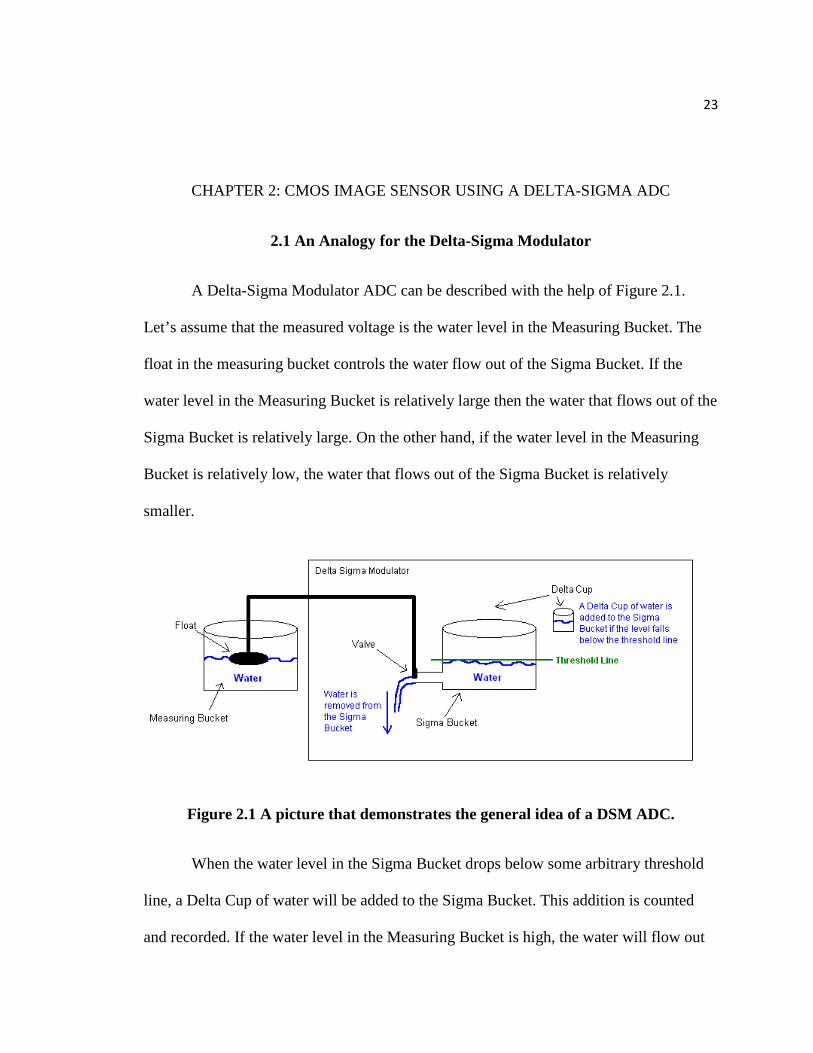
2.1 An Analogy for the Delta-Sigma Modulator
A Delta-Sigma Modulator ADC can be described with the help of Figure 2.1.
Let’s assume that the measured voltage is the water level in the Measuring Bucket. The
float in the measuring bucket controls the water flow out of the Sigma Bucket. If the
water level in the Measuring Bucket is relatively large then the water that flows out of the
Sigma Bucket is relatively large. On the other hand, if the water level in the Measuring
Bucket is relatively low, the water that flows out of the Sigma Bucket is relatively
smaller.
Figure 2.1 A picture that demonstrates the general idea of a DSM ADC.
When the water level in the Sigma Bucket drops below some arbitrary threshold
line, a Delta Cup of water will be added to the Sigma Bucket. This addition is counted
and recorded. If the water level in the Measuring Bucket is high, the water will flow out

24 of the Sigma Bucket at a fast rate and the number of times that a Delta Cup of water is
added per unit time will increase. On the other hand if the water level in the Measuring
Bucket is low, the water flowing out of the Sigma Bucket will be slower and the number
of times that a Delta Cup of water is added per unit time will decrease.
From this analogy, the water level in the Measuring Bucket can be determined by
averaging the number of times that water is added to the Sigma Bucket by the Delta Cup.
2.2 Sensing Scheme for a DSM in a CMOS Image Sensor
Figure 2.2 illustrates the sensing scheme used by a DSM in a CMOS Image
Sensor. There is one DSM for each column of pixels and the sensing occurs in parallel
for each column.
The sensing scheme begins with sampling the pixel’s reset signal onto the reset
sample and hold capacitor, CHR. This is accomplished by turning on the rowline and
ResetN signals on one of the multiple rows of pixels in the array. Each pixel on the
activated row will output its reset signal onto its respective column line. This reset signal
is then sampled onto the CHR capacitor through the activated SHR switch. Once the reset
signal is sampled, the rowline, ResetN, and SHR switches are turned off.

25
Figure 2.2 A 4x4 pixel diagram of a DSM CMOS Imager.

26
After the reset signal is sampled, the pixel is then exposed to light for a length of
time. Once the exposure time has expired, the same rowline and SHI switch is turned on.
This samples the image signal onto the image sample and hold capacitor, CHI. The
rowline and SHI switch is turned off once the image signal is sampled onto CHI.
Next, the DSM will take the reset and image input signals that were sampled on
the two CH capacitors and convert them to a digital code equivalent. The n-bit wide
counter that is connected at the end of the DSM will help the DSM convert the analog
input signals to a digital output code.
2.3 DSM Operation in a CMOS Image Sensor
Figure 2.3, shows the schematic diagram of a basic DSM sensing circuit in a
CMOS Image sensor [2]. The differential input signals, image, VIMAGE and reset, VRESET
are stored on the two different sample-and-hold capacitors that are connected to the gates
of the PMOS transistors M7 and M8 respectively. These transistors serve the purpose of a
source follower for the input signals to convert the input voltages into currents. These
input-voltages generate current sets, the amount of current that flows into the sigma
bucket. The voltage levels on the sources of the M7/M8 source-followers are equal to the
gate voltage plus a threshold as long as the width of the source-follower transistors, M7
and M8 are large. This relationship can, and will, be derived now. These source-followers
are operating in the saturation region. The equations governing their operation are

27
𝐼𝐼𝐼𝐼7,𝐼𝐼8 = 𝜇𝜇𝑝𝑝𝐶𝐶𝑅𝑅𝑜𝑜𝑊𝑊𝐼𝐼7,𝐼𝐼8
2𝐿𝐿𝐼𝐼7,𝐼𝐼8�𝑉𝑉𝑜𝑜𝐼𝐼7,𝐼𝐼8 − 𝑉𝑉𝑔𝑔𝐼𝐼7,𝐼𝐼8 + 𝑉𝑉𝑠𝑠ℎ𝐼𝐼7,𝐼𝐼8�
2 (2-1)
where: IM7,M8 Drain Current for transistor M7 and M8 (A)
µp Surface Mobility for the P-channel Transistor (cm2/Vs)
Cox Oxide Capacitance (fF/µm2)
WM7,M8 Width of transistor M7 and M8 (µm)
LM7,M8 Length of transistor M7 and M8 (µm)
VsM7,M8 Source voltage of transistor M7 and M8 (V)
VgM7,M8 Gate voltage of transistor M7 and M8 (V)
VthM7,M8 Threshold voltage of transistor M7 and M8 (V)
By rearranging the variables in Equation 2-1, the equation relating the source
voltage to the gate voltage is given in Equation 2-2 seen below. If the width-to-length
ratio for transistors M7 and M8 is large, Equation 2-2 can be simplified into Equation 2-
4. This reduction shows the voltages on the sources of transistors M7 and M8 are simply
the sum of the input gate voltages and the PMOS threshold voltage.
𝑉𝑉𝑜𝑜𝐼𝐼7,𝐼𝐼8 = 𝑉𝑉𝑔𝑔𝐼𝐼7,𝐼𝐼8 + 𝑉𝑉𝑠𝑠ℎ𝐼𝐼7,𝐼𝐼8 + �2𝐿𝐿𝐼𝐼7,𝐼𝐼8𝐼𝐼𝐼𝐼7,𝐼𝐼8𝜇𝜇𝑝𝑝𝐶𝐶𝑅𝑅𝑜𝑜 𝑊𝑊𝐼𝐼7,𝐼𝐼8
(2-2)
𝑉𝑉𝑜𝑜𝐼𝐼7,𝐼𝐼8 = 𝑉𝑉𝑔𝑔𝐼𝐼7,𝐼𝐼8 + 𝑉𝑉𝑠𝑠ℎ𝐼𝐼7,𝐼𝐼8 + 𝛿𝛿𝑠𝑠 ,𝑒𝑒𝑒𝑒𝑒𝑒𝑅𝑅𝑒𝑒 (2-3)
𝑉𝑉𝑜𝑜𝐼𝐼7,𝐼𝐼8 ≈ 𝑉𝑉𝑔𝑔𝐼𝐼7,𝐼𝐼8 + 𝑉𝑉𝑠𝑠ℎ𝐼𝐼7,𝐼𝐼8 (2-4)

28
Figure 2.3 Schematic of a Basic CMOS Imager Delta Sigma Modulator [2].
Simulations can be used to determine the optimal widths for the source follower
transistor so that the width error, δw,error is minimized. A DC sweep simulation is run on

29 the schematic shown in Figure 2.4. A total of 5 transistor sizes were simulated: 20λ (1.2
µm), 40λ (2.4 µm), 60λ (3.6 µm), 80λ (4.8 µm), and 100λ (6.0 µm). The VDD terminal is
set to 5V and the VSS terminal is connected to ground. The vin signal is swept from 5V to
0V.
Figure 2.4 Schematic to determine the optimum source-follower transistor size.
Figure 2.5 A DC sweep on the five PMOS source follower-transistor in Figure 2.4
with its source terminal as the output.

30
Figure 2.6 The slope of the source terminal (output) for the DC sweep simulation on
the five PMOS source-follower transistors in Figure 2.4.
From Figure 2.5, the PMOS source-follower with a width of 20λ does not track
well with the input signal, vin. As the vin signal approaches 0V, the source voltage on the
PMOS moves away from the vin signal. When the width of the source-follower increases
to 40λ, the source voltage diverts less when the input signal approaches 0V. This
diversion reduces as the width of the PMOS transistor increases. This is because the slope
of the source terminal changes less as the width of the transistor increases, as shown in
Figure 2.6. The source-follower with a width of 20λ has the greatest slope changes and
the source-follower with a width of 100λ has the least slope changes. The slope changes
for the source terminal between the 80λ and 100λ transistors are fairly similar. Therefore,

31 a width of 80λ or 4.8µm for the PMOS source-follower is adequate for this DSM (as
shown in Figure 2.3).
The PMOS source-followers in Figure 2.3, M7 and M8, have the body terminals
tied to their source terminals. This configuration is necessary because it eliminates any
source to body voltage, Vsb dependency in the threshold voltage. In other words, this
connection removes body-effect in these MOSFETS. Equation 2-5 shows the relationship
between the threshold voltage and source-to-body voltage, Vsb.
𝑉𝑉𝑠𝑠ℎ = 𝑉𝑉𝑠𝑠ℎ0 + 𝛾𝛾 ���2𝑉𝑉𝑑𝑑𝑝𝑝 � + 𝑉𝑉𝑜𝑜𝑠𝑠 − ��2𝑉𝑉𝑑𝑑𝑝𝑝 �� (2-5)
Where: Vth0 Threshold Voltage when the source to body voltage
is zero (V)
Vfp Flatband Voltage (V)
𝑉𝑉𝑜𝑜 = 𝑉𝑉𝑔𝑔 + 𝑉𝑉𝑠𝑠ℎ0 + 𝛾𝛾 ���2𝑉𝑉𝑑𝑑𝑝𝑝 � + 𝑉𝑉𝑜𝑜 − 𝑉𝑉𝑠𝑠 − ��2𝑉𝑉𝑑𝑑𝑝𝑝 �� + �2𝐿𝐿𝐼𝐼7,𝐼𝐼8𝐼𝐼𝐼𝐼7,𝐼𝐼8𝜇𝜇𝑝𝑝𝐶𝐶𝑅𝑅𝑜𝑜 𝑊𝑊𝐼𝐼7,𝐼𝐼8
(2-6)
The input-output transfer function of a source-follower with its body not tied to its
source will be nonlinear and it is shown in Equation 2-6. A DC sweep simulation, as seen
in Figure 2.7, is run to illustrate this nonlinearity. The PMOS transistor on the left has its
body connected to the source resulting in zero VSB. The PMOS transistor on the right has
its body connect to VDD that leads to a non-zero Vsb. In this simulation, the VDD
terminal is set to 5V and the VSS terminal is connected to ground. The vin signal is swept

32 from 5V to 0V. Figure 2.8 shows instantaneous slope of the source terminal for both of
the PMOS transistor. The PMOS source-follower with its body tied to its source has a
more constant slope than when its body not tied to its source. Therefore, it is required to
have the body of a source-follower tied to its source for a linear input-output transfer
function. The AMI C5 process used in the experimental results is not a twin-well process
and it is not possible to connect the body of an NMOS transistor to its source. Therefore,
a PMOS source-follower is used instead of a NMOS although a PMOS transistor has a
mobility that is half of a NMOS transistor.
Figure 2.7 A simulation schematic used to compare body-effect in PMOS source-
followers.
Transistors M1, M3 and M2, M4 with capacitor CLEFT and CRIGHT in Figure 2.3
serve the purpose as a forming switched-capacitor resistor in the DSM ADC. Node phi1B
and phi2B are connected to the inverted signals of a 2-phase non-overlapping clock. Its
frequency is equal to the master clock, fclk. Figure 2.9 shows the waveform of the 2-phase
non-overlapping clock signals, phi1, phi2, phi1B, and phi2B. Capacitor CLEFT and CRIGHT

33 are poly1-poly2 overlapped capacitors. The resistance of a switch capacitor resistor can
be derived, as seen below, and finally shown in Equation 2-7.
𝐼𝐼𝐶𝐶𝐿𝐿𝑅𝑅𝐿𝐿𝑅𝑅 ,𝑅𝑅𝐼𝐼𝐼𝐼𝐶𝐶𝑅𝑅 = 𝐶𝐶𝐿𝐿𝑅𝑅𝐿𝐿𝑅𝑅 ,𝑅𝑅𝐼𝐼𝐼𝐼𝐶𝐶𝑅𝑅∆𝑉𝑉𝐶𝐶𝐿𝐿𝑅𝑅𝐿𝐿𝑅𝑅 ,𝑅𝑅𝐼𝐼𝐼𝐼𝐶𝐶𝑅𝑅
∆𝑅𝑅
(2-4)
𝐼𝐼𝐶𝐶𝐿𝐿𝑅𝑅𝐿𝐿𝑅𝑅 ,𝑅𝑅𝐼𝐼𝐼𝐼𝐶𝐶𝑅𝑅 = 𝐶𝐶𝐿𝐿𝑅𝑅𝐿𝐿𝑅𝑅 ,𝑅𝑅𝐼𝐼𝐼𝐼𝐶𝐶𝑅𝑅∆𝑉𝑉𝐶𝐶𝐿𝐿𝑅𝑅𝐿𝐿𝑅𝑅 ,𝑅𝑅𝐼𝐼𝐼𝐼𝐶𝐶𝑅𝑅 𝑑𝑑𝑅𝑅𝑅𝑅𝑐𝑐
(2-5)
∆𝑉𝑉𝐶𝐶𝐿𝐿𝑅𝑅𝐿𝐿𝑅𝑅 ,𝑅𝑅𝐼𝐼𝐼𝐼𝐶𝐶𝑅𝑅𝐼𝐼𝐶𝐶𝐿𝐿𝑅𝑅𝐿𝐿𝑅𝑅 ,𝑅𝑅𝐼𝐼𝐼𝐼𝐶𝐶𝑅𝑅
= 1𝐶𝐶𝐿𝐿𝑅𝑅𝐿𝐿𝑅𝑅 ,𝑅𝑅𝐼𝐼𝐼𝐼𝐶𝐶𝑅𝑅 𝑑𝑑𝑅𝑅𝑅𝑅𝑐𝑐
(2-6)
𝑅𝑅𝑜𝑜𝑠𝑠𝑠𝑠𝑠𝑠𝑅𝑅 ℎ𝐶𝐶𝐶𝐶𝑝𝑝 = 1
𝐶𝐶𝐿𝐿𝑅𝑅𝐿𝐿𝑅𝑅 ,𝑅𝑅𝐼𝐼𝐼𝐼𝐶𝐶𝑅𝑅 𝑑𝑑𝑅𝑅𝑅𝑅𝑐𝑐
(2-7)
Figure 2.8 The differentiated output source voltage signal used to compare body-
effect in PMOS source-followers.
During the first half of the clock period (when phi1B is low and phi2B is high),
capacitor CLEFT and CRIGHT is charged up to VDD. On the next half of the clock period

34 (when phi1B is high and phi2B is low), some of the charge stored on CRIGHT will flow to
VSS. The amount of current flow from capacitor CRIGHT to VSS can be determined using
Equation 2-3 and Equation 2-7. Since we know that the initial voltage on CRIGHT is VDD
and the final voltage on CRIGHT is VRESET + Vth,M8, the magnitude of the reset current,
IRESET that flows is shown in Equation 2-10.
𝐼𝐼𝑅𝑅𝑅𝑅𝑅𝑅𝑅𝑅𝑅𝑅 =Δ𝑉𝑉𝐶𝐶𝑅𝑅𝐼𝐼𝐼𝐼𝐶𝐶𝑅𝑅𝑅𝑅𝐶𝐶𝑅𝑅𝐼𝐼𝐼𝐼𝐶𝐶𝑅𝑅
(2-8)
𝐼𝐼𝑅𝑅𝑅𝑅𝑅𝑅𝑅𝑅𝑅𝑅 =𝑉𝑉𝑠𝑠𝑅𝑅𝑠𝑠𝑠𝑠𝑠𝑠𝐶𝐶𝑅𝑅 ,𝐶𝐶𝑅𝑅𝐼𝐼𝐼𝐼𝐶𝐶𝑅𝑅 −𝑉𝑉𝑑𝑑𝑠𝑠𝑅𝑅𝐶𝐶𝑅𝑅 ,𝐶𝐶𝑅𝑅𝐼𝐼𝐼𝐼𝐶𝐶𝑅𝑅
𝑅𝑅𝐶𝐶𝑅𝑅𝐼𝐼𝐼𝐼𝐶𝐶𝑅𝑅= 𝑉𝑉𝐴𝐴𝐴𝐴−�𝑉𝑉𝑅𝑅𝑅𝑅𝑅𝑅𝑅𝑅𝑅𝑅 +𝑉𝑉𝑠𝑠ℎ ,𝐼𝐼8�
1𝐶𝐶𝑅𝑅𝐼𝐼𝐼𝐼𝐶𝐶𝑅𝑅 𝑑𝑑𝑅𝑅𝑅𝑅𝑐𝑐
(2-9)
𝐼𝐼𝑅𝑅𝑅𝑅𝑅𝑅𝑅𝑅𝑅𝑅 = 𝐶𝐶𝑅𝑅𝐼𝐼𝐼𝐼𝐶𝐶𝑅𝑅𝑑𝑑𝑅𝑅𝑅𝑅𝑐𝑐 �𝑉𝑉𝐴𝐴𝐴𝐴 − 𝑉𝑉𝑅𝑅𝑅𝑅𝑅𝑅𝑅𝑅𝑅𝑅 − 𝑉𝑉𝑠𝑠ℎ ,𝐼𝐼8� (2-10)
Figure 2.9 The waveform of a 2-phase non-overlapping clock.

35 The reset current, IRESET will be mirrored over to the image branch through the
current mirror transistors, M9 and M10. Assuming transistor M9 and M10 has identical
threshold voltages and the drain voltages, the reset current, IRESET will be exactly equal to
the mirrored reset current, IRESET,mirror as shown in Equation 2-11.
𝐼𝐼𝑅𝑅𝑅𝑅𝑅𝑅𝑅𝑅𝑅𝑅 ,𝑅𝑅𝑠𝑠𝑒𝑒𝑒𝑒𝑅𝑅𝑒𝑒 = 𝐶𝐶𝑅𝑅𝐼𝐼𝐼𝐼𝐶𝐶𝑅𝑅𝑑𝑑𝑅𝑅𝑅𝑅𝑐𝑐 �𝑉𝑉𝐴𝐴𝐴𝐴 − 𝑉𝑉𝑅𝑅𝑅𝑅𝑅𝑅𝑅𝑅𝑅𝑅 − 𝑉𝑉𝑠𝑠ℎ ,𝐼𝐼8� (2-11)
The right branch of the DSM, which is connected to the VRESET input signal serve
the role as the float and valve in Figure 2.1. This unit controls the amount of charge
removed from the sigma bucket. Capacitor CBUCKL is serves the role as a “Sigma Bucket”
in Figure 2.1 and it is also formed from poly1-poly2 overlapped.
During the first phase of the clock (phi1 is VDD and phi2 is VSS), the sense-amp
(clocked comparator) turns transistor M5 off by taking the setting the negative terminal
of the sense-amp to VDD. At the end of the first clock phase, the sense-amp senses the
voltage difference between net_buckL and net_buckR and turns on M5 if the voltage on
net_buckR is higher than net_buckL. The sense-amp will keep M5 off, if the voltage
level on net_buckR is lower than net_buckL. An image current, IIMAGE will flow from
CLEFT into CBUCKL if M5 is turned on. This current will raise the voltage on capacitor
CBUCKL. This image current serves the role of the “Delta Cup” as seen in Figure 2.1. This
process will repeat N times over the entire conversion period. During this period, the
sense-amp will turn on M5 for M times. The average image current, IIMAGE over N
measurements can be derived using Equation 2-3 and Equation 2-7 and the final equation
is shown in Equation 2-14.

36
𝐼𝐼𝐼𝐼𝐼𝐼𝐼𝐼𝐼𝐼𝑅𝑅 = 𝐼𝐼𝑁𝑁
𝑉𝑉𝐶𝐶𝐿𝐿𝑅𝑅𝐿𝐿𝑅𝑅𝑅𝑅𝐶𝐶𝐿𝐿𝑅𝑅𝐿𝐿𝑅𝑅
(2-12)
𝐼𝐼𝐼𝐼𝐼𝐼𝐼𝐼𝐼𝐼𝑅𝑅 = 𝐼𝐼𝑁𝑁�𝑉𝑉𝑠𝑠𝑅𝑅𝑠𝑠𝑠𝑠𝑠𝑠𝐶𝐶𝑅𝑅 ,𝐶𝐶𝐿𝐿𝑅𝑅𝐿𝐿𝑅𝑅 −𝑉𝑉𝑑𝑑𝑠𝑠𝑅𝑅𝐶𝐶𝑅𝑅 ,𝐶𝐶𝐿𝐿𝑅𝑅𝐿𝐿𝑅𝑅
𝑅𝑅𝐶𝐶𝐿𝐿𝑅𝑅𝐿𝐿𝑅𝑅� = 𝐼𝐼
𝑁𝑁�𝑉𝑉𝐴𝐴𝐴𝐴−�𝑉𝑉𝐼𝐼𝐼𝐼𝐼𝐼𝐼𝐼𝑅𝑅 +𝑉𝑉𝑠𝑠ℎ ,𝐼𝐼7�
1𝐶𝐶𝐿𝐿𝑅𝑅𝐿𝐿𝑅𝑅 𝑑𝑑𝑅𝑅𝑅𝑅𝑐𝑐
�
(2-13)
𝐼𝐼𝐼𝐼𝐼𝐼𝐼𝐼𝐼𝐼𝑅𝑅 = 𝐼𝐼𝑁𝑁𝐶𝐶𝐿𝐿𝑅𝑅𝐿𝐿𝑅𝑅𝑑𝑑𝑅𝑅𝑅𝑅𝑐𝑐 �𝑉𝑉𝐴𝐴𝐴𝐴 − 𝑉𝑉𝐼𝐼𝐼𝐼𝐼𝐼𝐼𝐼𝑅𝑅 − 𝑉𝑉𝑠𝑠ℎ ,𝐼𝐼7� (2-14)
Over a long period of time, the current into and out of the sigma bucket, CBUCKL is
identical. Therefore, the image and reference current are equal to each other. Equation 2-
17 shows the input-output transfer function that relates the analog input signal VIMAGE and
VRESET to the digital code M over N measurements.
𝐼𝐼𝐼𝐼𝐼𝐼𝐼𝐼𝐼𝐼𝑅𝑅 = 𝐼𝐼𝑅𝑅𝑅𝑅𝑅𝑅𝑅𝑅𝑅𝑅,𝑅𝑅𝑠𝑠𝑒𝑒𝑒𝑒𝑅𝑅𝑒𝑒
(2-15)
𝐼𝐼𝑁𝑁𝐶𝐶𝐿𝐿𝑅𝑅𝐿𝐿𝑅𝑅𝑑𝑑𝑝𝑝ℎ𝑠𝑠�𝑉𝑉𝐴𝐴𝐴𝐴 − 𝑉𝑉𝐼𝐼𝐼𝐼𝐼𝐼𝐼𝐼𝑅𝑅 − 𝑉𝑉𝑠𝑠ℎ ,𝐼𝐼7� = 𝐶𝐶𝑅𝑅𝐼𝐼𝐼𝐼𝐶𝐶𝑅𝑅𝑑𝑑𝑝𝑝ℎ𝑠𝑠�𝑉𝑉𝐴𝐴𝐴𝐴 − 𝑉𝑉𝑅𝑅𝑅𝑅𝑅𝑅𝑅𝑅𝑅𝑅 − 𝑉𝑉𝑠𝑠ℎ ,𝐼𝐼8�
(2-16)
𝐼𝐼 = 𝑁𝑁 𝐶𝐶𝑅𝑅𝐼𝐼𝐼𝐼𝐶𝐶𝑅𝑅𝐶𝐶𝐿𝐿𝑅𝑅𝐿𝐿𝑅𝑅
�𝑉𝑉𝐴𝐴𝐴𝐴−𝑉𝑉𝑅𝑅𝑅𝑅𝑅𝑅𝑅𝑅𝑅𝑅 −𝑉𝑉𝑠𝑠ℎ ,𝐼𝐼8��𝑉𝑉𝐴𝐴𝐴𝐴−𝑉𝑉𝐼𝐼𝐼𝐼𝐼𝐼𝐼𝐼𝑅𝑅 −𝑉𝑉𝑠𝑠ℎ ,𝐼𝐼7� (2-17)
The input-output transfer function for this CMOS DSM architecture is non-linear
which is undesirable in some situations (though in some situation, extremely bright or
dark images may be desirable). To demonstrate this in more detail, let’s assume N is 100,
VDD is 5V, VRESET is 3V, both Vth,M7 and Vth,M8 is 1V, and CLEFT and CRIGHT are identical.

37 Figure 2.10 shows the input-output transfer function curve for this basic CMOS Imager
DSM.
Figure 2.10 Basic CMOS Imager DSM Input-Output Transfer Function.
2.4 CMOS Image Sensor DSM with Reference Path
One of the biggest drawbacks in the DSM architecture discussed in Section 2.3 is
that the input-output transfer function is non-linear. The input-output transfer function
can be made linear by introducing a reference path to the basic CMOS Image Sensor
DSM architecture [2]. Figure 2.11 shows the schematic of a DSM with reference path.
Transistors M9, M10, M11, and M12 constitute the reference path.
0
20
40
60
80
100
120
0 0.5 1 1.5 2 2.5 3 3.5
M
Count
VIMAGE (V)
Basic DSM Transfer Function
Ideal

38
Figure 2.11 Schematic of a CMOS Imager Delta Sigma Modulator with reference
path [2].
The magnitude of the reset current, IRESET in this architecture is similar to the reset
current in the basic DSM, which is shown in Equation 2-10. However, the magnitude
image current, IIMAGE in this architecture is different than the image current in the basic
DSM. In this architecture, the image current flows into CBUCKL at every clocked cycle,
whereas in the basic DSM, the image current only flows into CBUCKL when the voltage on

39 net_buckR is higher than net_buckL. The magnitude of the image current, IIMAGE for this
DSM architecture is
𝐼𝐼𝐼𝐼𝐼𝐼𝐼𝐼𝐼𝐼𝑅𝑅 = 𝐶𝐶𝐿𝐿𝑅𝑅𝐿𝐿𝑅𝑅𝑑𝑑𝑅𝑅𝑅𝑅𝑐𝑐 �𝑉𝑉𝐴𝐴𝐴𝐴 − 𝑉𝑉𝐼𝐼𝐼𝐼𝐼𝐼𝐼𝐼𝑅𝑅 − 𝑉𝑉𝑠𝑠ℎ ,𝐼𝐼5� (2-18)
In this architecture, the output of the sense-amp is connected to transistor M11
instead. For the entire time of the first clock phase, the sense-amp turns off M11. At the
end of the first clock phase, the sense-amp measures the voltage level on net_buckL and
net_buckR and turns on M11 if the voltage level on net_buckL is higher than net_buckR.
M11 remains off if the voltage level on net_buckL is lower than net_buckR. This process
repeats for N times over the entire conversion period. During this period, M11 turns on
for M amount of times and the average IVREF current that flows is given by
𝐼𝐼𝑅𝑅𝑅𝑅𝐿𝐿 = 𝐼𝐼𝑁𝑁
∆𝑉𝑉𝐶𝐶𝑅𝑅𝑅𝑅𝐿𝐿𝑅𝑅𝐶𝐶𝑅𝑅𝑅𝑅𝐿𝐿
(2-19)
𝐼𝐼𝑅𝑅𝑅𝑅𝐿𝐿 = 𝐼𝐼𝑁𝑁�𝑉𝑉𝑠𝑠𝑅𝑅𝑠𝑠𝑠𝑠𝑠𝑠𝐶𝐶𝑅𝑅 ,𝐶𝐶𝑅𝑅𝑅𝑅𝐿𝐿 −𝑉𝑉𝑑𝑑𝑠𝑠𝑅𝑅𝐶𝐶𝑅𝑅 ,𝐶𝐶𝑅𝑅𝑅𝑅𝐿𝐿
𝑅𝑅𝐶𝐶𝑅𝑅𝑅𝑅𝐿𝐿� = 𝐼𝐼
𝑁𝑁�𝑉𝑉𝐴𝐴𝐴𝐴−�𝑉𝑉𝑅𝑅𝑅𝑅𝐿𝐿 +𝑉𝑉𝑠𝑠ℎ ,𝐼𝐼12�
1𝐶𝐶𝑅𝑅𝑅𝑅𝐿𝐿 𝑑𝑑𝑅𝑅𝑅𝑅𝑐𝑐
�
(2-20)
𝐼𝐼𝑅𝑅𝑅𝑅𝐿𝐿 = 𝐼𝐼𝑁𝑁𝐶𝐶𝑅𝑅𝑅𝑅𝐿𝐿𝑑𝑑𝑅𝑅𝑅𝑅𝑐𝑐 �𝑉𝑉𝐴𝐴𝐴𝐴 − 𝑉𝑉𝑅𝑅𝑅𝑅𝐿𝐿 − 𝑉𝑉𝑠𝑠ℎ ,𝐼𝐼12� (2-21)
The DSM discussed in Section 2.3, mirrors the IRESET current from the right
branch to the left branch of the DSM. For this DSM, the IIMAGE is mirrored from the left
branch to the right branch of the DSM instead. The mirrored image current, IIMAGE,mirror is
equivalent to the image current, IIMAGE if the drain voltage on M7 and M8 is identical.

40
𝐼𝐼𝐼𝐼𝐼𝐼𝐼𝐼𝐼𝐼𝑅𝑅 ,𝑅𝑅𝑠𝑠𝑒𝑒𝑒𝑒𝑅𝑅𝑒𝑒 = 𝐼𝐼𝐼𝐼𝐼𝐼𝐼𝐼𝐼𝐼𝑅𝑅 (2-22)
𝐼𝐼𝐼𝐼𝐼𝐼𝐼𝐼𝐼𝐼𝑅𝑅 ,𝑅𝑅𝑠𝑠𝑒𝑒𝑒𝑒𝑅𝑅𝑒𝑒 = 𝐶𝐶𝐿𝐿𝑅𝑅𝐿𝐿𝑅𝑅𝑑𝑑𝑅𝑅𝑅𝑅𝑐𝑐 �𝑉𝑉𝐴𝐴𝐴𝐴 − 𝑉𝑉𝐼𝐼 − 𝑉𝑉𝑠𝑠ℎ ,𝐼𝐼5� (2-23)
For this DSM, CBUCKR is the sigma bucket. Over N clocked cycles, the sum of
current into and out of the sigma bucket is identical. Equation 2-26 shows the input-
output transfer function for this reference path DSM architecture. This equation relates
the analog input signal, VIMAGE and VRESET and the reference signal, VREF to the digital
code M over N measurements.
𝐼𝐼𝐼𝐼𝐼𝐼𝐼𝐼𝐼𝐼𝑅𝑅 = 𝐼𝐼𝑅𝑅𝑅𝑅𝑅𝑅𝑅𝑅𝑅𝑅 + 𝐼𝐼𝑅𝑅𝑅𝑅𝐿𝐿 (2-24)
𝐶𝐶𝐿𝐿𝑅𝑅𝐿𝐿𝑅𝑅𝑑𝑑𝑅𝑅𝑅𝑅𝑐𝑐 �𝑉𝑉𝐴𝐴𝐴𝐴 − 𝑉𝑉𝐼𝐼𝐼𝐼𝐼𝐼𝐼𝐼𝑅𝑅 − 𝑉𝑉𝑠𝑠ℎ ,𝐼𝐼5� =
𝐶𝐶𝑅𝑅𝐼𝐼𝐼𝐼𝐶𝐶𝑅𝑅𝑑𝑑𝑅𝑅𝑅𝑅𝑐𝑐 �𝑉𝑉𝐴𝐴𝐴𝐴 − 𝑉𝑉𝑅𝑅𝑅𝑅𝑅𝑅𝑅𝑅𝑅𝑅 − 𝑉𝑉𝑠𝑠ℎ ,𝐼𝐼6� + 𝐼𝐼𝑁𝑁𝐶𝐶𝑅𝑅𝑅𝑅𝐿𝐿𝑑𝑑𝑅𝑅𝑅𝑅𝑐𝑐 �𝑉𝑉𝐴𝐴𝐴𝐴 − 𝑉𝑉𝑅𝑅𝑅𝑅𝐿𝐿 − 𝑉𝑉𝑠𝑠ℎ ,𝐼𝐼12�
(2-25)
𝐼𝐼 = 𝑁𝑁 (𝐶𝐶𝐿𝐿𝑅𝑅𝐿𝐿𝑅𝑅 −𝐶𝐶𝑅𝑅𝐼𝐼𝐼𝐼𝐶𝐶𝑅𝑅 )𝑉𝑉𝐴𝐴𝐴𝐴+(𝐶𝐶𝑅𝑅𝐼𝐼𝐼𝐼𝐶𝐶𝑅𝑅 𝑉𝑉𝑅𝑅𝑅𝑅𝑅𝑅𝑅𝑅𝑅𝑅 −𝐶𝐶𝐿𝐿𝑅𝑅𝐿𝐿𝑅𝑅 𝑉𝑉𝐼𝐼𝐼𝐼𝐼𝐼𝐼𝐼𝑅𝑅 )+�𝐶𝐶𝑅𝑅𝐼𝐼𝐼𝐼𝐶𝐶𝑅𝑅 𝑉𝑉𝑠𝑠ℎ ,𝐼𝐼6−𝐶𝐶𝐿𝐿𝑅𝑅𝐿𝐿𝑅𝑅 𝑉𝑉𝑠𝑠ℎ ,𝐼𝐼5�𝐶𝐶𝑅𝑅𝑅𝑅𝐿𝐿 �𝑉𝑉𝐴𝐴𝐴𝐴−𝑉𝑉𝑅𝑅𝑅𝑅𝐿𝐿−𝑉𝑉𝑠𝑠ℎ ,𝐼𝐼12�
(2-26)
𝐼𝐼 = 𝑁𝑁 𝐶𝐶𝐿𝐿𝑅𝑅𝐿𝐿𝑅𝑅 ,𝑅𝑅𝐼𝐼𝐼𝐼𝐶𝐶𝑅𝑅 �𝑉𝑉𝑅𝑅𝑅𝑅𝑅𝑅𝑅𝑅𝑅𝑅 −𝑉𝑉𝐼𝐼𝐼𝐼𝐼𝐼𝐼𝐼𝑅𝑅 +𝑉𝑉𝑠𝑠ℎ ,𝐼𝐼6−𝑉𝑉𝑠𝑠ℎ ,𝐼𝐼5�𝐶𝐶𝑅𝑅𝑅𝑅𝐿𝐿 �𝑉𝑉𝐴𝐴𝐴𝐴−𝑉𝑉𝑅𝑅𝑅𝑅𝐿𝐿 −𝑉𝑉𝑠𝑠ℎ ,𝐼𝐼12� (2-27)
If the capacitance of CLEFT and CRIGHT are identical, Equation 2-26 can be
simplified to Equation 2-27 and the input transfer function for this DSM architecture is
linear. To demonstrate this in more detail, let’s assume N is 100, VDD is 5V, VRESET is

41
3V, VREF is 1V, Vth,M5, Vth,M6, and Vth,M12 is also 1V, and CLEFT,RIGHT and CVREF are
identical. Figure 2.12 shows the input-output transfer function for this DSM.
Figure 2.12 CMOS Imager DSM with Reference Path Input-Output Transfer
Function.
Although this DSM has a linear transfer function, the transfer function is very
susceptible to transistor threshold voltage mismatches. A fixed pattern noise between the
columns will occur if the threshold voltage on M5, M6 and M12 are not identical
between all the DSMs in the array. A voltage threshold mismatch on M5 and M6 will
cause an offset error in the transfer function and a voltage threshold mismatch on M12
will induce a gain error in the transfer function instead. An offset error will either shift
0
20
40
60
80
100
120
00.511.522.533.5
M
Count
VIMAGE (V)
DSM with Reference Path Transfer Function
Ideal

42 the transfer function upwards or downwards from ideal. On the other hand, a gain error
will either increase or decrease the slope of the transfer function.
Figure 2.13 illustrates the behavior of the transfer function when threshold voltage
mismatches on M5, M6 and M12 exist. The red line in Figure 2.13 is the transfer function
of the DSM when a 0.25V threshold voltage delta between transistor M5 and M6 exist.
The red line illustrates an offset error. On the other hand, the green line is the transfer
function of the DSM when there is a 0.2V threshold mismatch on M12 and it illustrates a
gain error.
Figure 2.13 Comparing the ideal transfer function of a Reference Path CMOS
Imager DSM to a transfer function with different threshold voltage mismatches.
0
20
40
60
80
100
120
01234
M
Count
VIMAGE (V)
Comparing the Reference Path DSM to one with Vth mismatches
Ideal
Offset Error, Vth_M5-Vth_M6 mismatch
Gain Error, Vth_M12 mismatch

43
2.5 CMOS Image Sensor DSM with Reference Path and Input Path Switching
As discussed in Section 2.4, an offset error will occur in the input-output transfer
function if there is any voltage threshold mismatch in the input transistors (M5 and M6 of
Figure 2.11). A technique called input path switching can be used to eliminate offset error
in the transfer function [1],[2]. The input path switching technique divides the whole
conversion period into two equal halves (N/2 clock cycles). During the first half of the
conversion period, the operation of the DSM does not differ from the sensing operation
described in Section 2.4. However, on the second half of the conversion period, the DSM
reverses its input terminals. The image input signal, VIMAGE and the reset input signal,
VRESET switches gate connections. The digital output codes at the end of both halves of the
sensing period are added together to get the final digital output code. This digital output
code will be free from offset error.
Figure 2.14 shows the CMOS imager DSM with both reference path and input
path switching improvements. For the first half of the sensing period, the path select
control signals, SLT and SLB are set to VDD and VSS respectively. This configuration
connects the image input signal, VINPUT to the gate of M5 through M1S and the reset input
signal, VRESET is connected to the gate of M6 through M3S. With this, the left branch
current, ILEFT,t=1 and right branch current, IRIGHT,t=1 for the first half of sensing period are
given by
𝐼𝐼𝐿𝐿𝑅𝑅𝐿𝐿𝑅𝑅 ,𝑠𝑠=1 = 𝐶𝐶𝐿𝐿𝑅𝑅𝐿𝐿𝑅𝑅𝑑𝑑𝑅𝑅𝑅𝑅𝑐𝑐 �𝑉𝑉𝐴𝐴𝐴𝐴 − 𝑉𝑉𝐼𝐼𝐼𝐼𝐼𝐼𝐼𝐼𝑅𝑅 − 𝑉𝑉𝑠𝑠ℎ ,𝐼𝐼5� (2-28)
𝐼𝐼𝑅𝑅𝐼𝐼𝐼𝐼𝐶𝐶𝑅𝑅 ,𝑠𝑠=1 = 𝐶𝐶𝑅𝑅𝐼𝐼𝐼𝐼𝐶𝐶𝑅𝑅𝑑𝑑𝑅𝑅𝑅𝑅𝑐𝑐 �𝑉𝑉𝐴𝐴𝐴𝐴 − 𝑉𝑉𝑅𝑅𝑅𝑅𝑅𝑅𝑅𝑅𝑅𝑅 − 𝑉𝑉𝑠𝑠ℎ ,𝐼𝐼6� (2-29)

44 In addition, the reference path is connected to the right branch of the DSM through
M14S.
Figure 2.14 Schematic of a CMOS Imager Delta Sigma Modulator with reference
path and input path switching [1].
For the entire conversion period, the positive and negative input terminals of the
sense-amp are connected to net_buckR and net_buckL respectively. M5S, M6S, M7S,
and M8S form a 2-bit analog multiplexer that steers either the negative or positive output
of the sense-amp to the output terminal of the DSM, M. For this half of the conversion
period, the positive terminal of the sense-amp is connected to the output of the DSM.

45 Another 2-bit analog multiplexer (M9S, M10S, M11S, and M12S) is needed to control
which output terminal of the sense-amp is connected to the gate of M11. The negative
terminal of the sense-amp is connected to the gate of M11 during the first half of the
conversion period.
Just like before, the sense-amp turns on M11 if the voltage level on net_buckL is
higher than net_buckR and leaves M11 off if the voltage level on net_buckL is lower
than net_buckR,. M11 will be turned on Mt=1 times for the first half of the conversion
period and the average reference current, IREF,t=1 that flows during this period is given by
𝐼𝐼𝑅𝑅𝑅𝑅𝐿𝐿 ,𝑠𝑠=1 = 𝐼𝐼𝑠𝑠=1𝑁𝑁2
𝑉𝑉𝐶𝐶𝑅𝑅𝑅𝑅𝐿𝐿𝑅𝑅𝐶𝐶𝑅𝑅𝑅𝑅𝐿𝐿
(2-30)
𝐼𝐼𝑅𝑅𝑅𝑅𝐿𝐿 ,𝑠𝑠=1 = 2 𝐼𝐼𝑠𝑠=1𝑁𝑁
�𝑉𝑉𝑠𝑠𝑅𝑅𝑠𝑠𝑠𝑠𝑠𝑠𝐶𝐶𝑅𝑅 ,𝐶𝐶𝑅𝑅𝑅𝑅𝐿𝐿 −𝑉𝑉𝑑𝑑𝑠𝑠𝑅𝑅𝐶𝐶 𝑅𝑅 ,𝐶𝐶𝑅𝑅𝑅𝑅𝐿𝐿
𝑅𝑅𝐶𝐶𝑅𝑅𝑅𝑅𝐿𝐿� = 2 𝐼𝐼𝑠𝑠=1
𝑁𝑁�𝑉𝑉𝐴𝐴𝐴𝐴−�𝑉𝑉𝑅𝑅𝑅𝑅𝐿𝐿 +𝑉𝑉𝑠𝑠ℎ ,𝐼𝐼12�
1𝐶𝐶𝑅𝑅𝑅𝑅𝐿𝐿 𝑑𝑑𝑅𝑅𝑅𝑅𝑐𝑐
�
(2-31)
𝐼𝐼𝑅𝑅𝑅𝑅𝐿𝐿 ,𝑠𝑠=1 = 2 𝐼𝐼𝑠𝑠=1𝑁𝑁
𝐶𝐶𝑅𝑅𝑅𝑅𝐿𝐿𝑑𝑑𝑅𝑅𝑅𝑅𝑐𝑐 �𝑉𝑉𝐴𝐴𝐴𝐴 − 𝑉𝑉𝑅𝑅𝑅𝑅𝐿𝐿 − 𝑉𝑉𝑠𝑠ℎ ,𝐼𝐼12� (2-32)
ILEFT,t=1 flow through the drain of M7 and it is mirrored over to the drain of M8.
Over N/2 clock cycles, the sum of currents into CBUCKR is zero. Therefore, the digital
code representation, Mt=1 of the analog input signals, VIMAGE and VRESET during the first
half of the sensing period is determined using the following
𝐼𝐼𝐿𝐿𝑅𝑅𝐿𝐿𝑅𝑅 ,𝑅𝑅𝑠𝑠𝑒𝑒𝑒𝑒𝑅𝑅 𝑒𝑒 ,𝑠𝑠=1 = 𝐼𝐼𝐿𝐿𝑅𝑅𝐿𝐿𝑅𝑅 ,𝑠𝑠=1 (2-33)
𝐼𝐼𝑅𝑅𝐼𝐼𝐼𝐼𝐶𝐶𝑅𝑅 ,𝑠𝑠=1 + 𝐼𝐼𝑅𝑅𝑅𝑅𝐿𝐿 ,𝑠𝑠=1 = 𝐼𝐼𝐿𝐿𝑅𝑅𝐿𝐿𝑅𝑅 ,𝑠𝑠=1 (2-34)

46 𝐶𝐶𝑅𝑅𝐼𝐼𝐼𝐼𝐶𝐶𝑅𝑅𝑑𝑑𝑅𝑅𝑅𝑅𝑐𝑐 �𝑉𝑉𝐴𝐴𝐴𝐴 − 𝑉𝑉𝑅𝑅𝑅𝑅𝑅𝑅𝑅𝑅𝑅𝑅 − 𝑉𝑉𝑠𝑠ℎ ,𝐼𝐼6� + 2 𝐼𝐼𝑠𝑠=1
𝑁𝑁𝐶𝐶𝑅𝑅𝑅𝑅𝐿𝐿𝑑𝑑𝑅𝑅𝑅𝑅𝑐𝑐 �𝑉𝑉𝐴𝐴𝐴𝐴 − 𝑉𝑉𝑅𝑅𝑅𝑅𝐿𝐿 − 𝑉𝑉𝑠𝑠ℎ ,𝐼𝐼12�
= 𝐶𝐶𝐿𝐿𝑅𝑅𝐿𝐿𝑅𝑅𝑑𝑑𝑅𝑅𝑅𝑅𝑐𝑐 �𝑉𝑉𝐴𝐴𝐴𝐴 − 𝑉𝑉𝐼𝐼𝐼𝐼𝐼𝐼𝐼𝐼𝑅𝑅 − 𝑉𝑉𝑠𝑠ℎ ,𝐼𝐼5� (2-35)
𝐼𝐼𝑠𝑠=1 = 𝑁𝑁2�𝐶𝐶𝐿𝐿𝑅𝑅𝐿𝐿𝑅𝑅 �𝑉𝑉𝐴𝐴𝐴𝐴−𝑉𝑉𝐼𝐼𝐼𝐼𝐼𝐼𝐼𝐼𝑅𝑅 −𝑉𝑉𝑠𝑠ℎ ,𝐼𝐼5�−𝐶𝐶𝑅𝑅𝐼𝐼𝐼𝐼𝐶𝐶𝑅𝑅 �𝑉𝑉𝐴𝐴𝐴𝐴−𝑉𝑉𝑅𝑅𝑅𝑅𝑅𝑅𝑅𝑅𝑅𝑅 −𝑉𝑉𝑠𝑠ℎ ,𝐼𝐼6�
𝐶𝐶𝑅𝑅𝑅𝑅𝐿𝐿 �𝑉𝑉𝐴𝐴𝐴𝐴−𝑉𝑉𝑅𝑅𝑅𝑅𝐿𝐿 −𝑉𝑉𝑠𝑠ℎ ,𝐼𝐼12� � (2-36)
Moving on to the second half of the sensing period, the path control signals, SLT
and SLB are set to VSS and VDD respectively. This will connect VIMAGE to the gate of M8
through M2S andVRESET is connected to the gate of M7 through M4S instead. The left
branch current, ILEFT,t=2 and right branch current, IRIGHT,t=2 for the second half of sensing
period are given by
𝐼𝐼𝐿𝐿𝑅𝑅𝐿𝐿𝑅𝑅 ,𝑠𝑠=2 = 𝐶𝐶𝐿𝐿𝑅𝑅𝐿𝐿𝑅𝑅𝑑𝑑𝑅𝑅𝑅𝑅𝑐𝑐 �𝑉𝑉𝐴𝐴𝐴𝐴 − 𝑉𝑉𝑅𝑅𝑅𝑅𝑅𝑅𝑅𝑅𝑅𝑅 − 𝑉𝑉𝑠𝑠ℎ ,𝐼𝐼5� (2-37)
𝐼𝐼𝑅𝑅𝐼𝐼𝐼𝐼𝐶𝐶𝑅𝑅 ,𝑠𝑠=2 = 𝐶𝐶𝑅𝑅𝐼𝐼𝐼𝐼𝐶𝐶𝑅𝑅𝑑𝑑𝑅𝑅𝑅𝑅𝑐𝑐 �𝑉𝑉𝐴𝐴𝐴𝐴 − 𝑉𝑉𝐼𝐼𝐼𝐼𝐼𝐼𝐼𝐼𝑅𝑅 − 𝑉𝑉𝑠𝑠ℎ ,𝐼𝐼6� (2-38)
The reference path is connected to the left branch of the DSM through M13S.
For the second half of the sensing period, the output of the DSM and the gate of
M11 are connected to the negative and positive terminal of the sense-amp instead.
Whenever the voltage level on net_buckL is lower than net_buckR, the sense-amp turns
on M11 and it is turned on for Mt=2 times. The average reference current, IREF,t=2 that
flows during this period is
𝐼𝐼𝑅𝑅𝑅𝑅𝐿𝐿 ,𝑠𝑠=2 = 2 𝐼𝐼𝑠𝑠=2𝑁𝑁
𝐶𝐶𝑅𝑅𝑅𝑅𝐿𝐿𝑑𝑑𝑅𝑅𝑅𝑅𝑐𝑐 �𝑉𝑉𝐴𝐴𝐴𝐴 − 𝑉𝑉𝑅𝑅𝑅𝑅𝐿𝐿 − 𝑉𝑉𝑠𝑠ℎ ,𝐼𝐼12� (2-39)

47 For this period of the sensing cycle, both the left branch current, ILEFT,t=2 and the
reference current, IREF,t=2 flow through the drain of M7 and is mirrored over to the drain
of M8. Just like the first half of the sensing period, the sum of current into CBUCKR is zero.
The digital code representation, Mt=2 of the analog input signal, VIMAGE and VRESET during
the second half of the sensing period is
𝐼𝐼𝐿𝐿𝑅𝑅𝐿𝐿𝑅𝑅 ,𝑅𝑅𝑠𝑠𝑒𝑒𝑒𝑒𝑅𝑅𝑒𝑒 ,𝑠𝑠=2 = 𝐼𝐼𝐿𝐿𝑅𝑅𝐿𝐿𝑅𝑅 ,𝑠𝑠=2+𝐼𝐼𝑅𝑅𝑅𝑅𝐿𝐿 ,𝑠𝑠=2 (2-40)
𝐼𝐼𝑅𝑅𝐼𝐼𝐼𝐼𝐶𝐶𝑅𝑅 ,𝑠𝑠=2 = 𝐼𝐼𝐿𝐿𝑅𝑅𝐿𝐿𝑅𝑅 ,𝑠𝑠=2+𝐼𝐼𝑉𝑉𝑅𝑅𝑅𝑅𝐿𝐿 ,𝑠𝑠=2 (2-41)
𝐶𝐶𝑅𝑅𝐼𝐼𝐼𝐼𝐶𝐶𝑅𝑅𝑑𝑑𝑅𝑅𝑅𝑅𝑐𝑐 �𝑉𝑉𝐴𝐴𝐴𝐴 − 𝑉𝑉𝐼𝐼𝐼𝐼𝐼𝐼𝐼𝐼𝑅𝑅 − 𝑉𝑉𝑠𝑠ℎ ,𝐼𝐼6� = 𝐶𝐶𝐿𝐿𝑅𝑅𝐿𝐿𝑅𝑅𝑑𝑑𝑅𝑅𝑅𝑅𝑐𝑐 �𝑉𝑉𝐴𝐴𝐴𝐴 − 𝑉𝑉𝑅𝑅𝑅𝑅𝑅𝑅𝑅𝑅𝑅𝑅 − 𝑉𝑉𝑠𝑠ℎ ,𝐼𝐼5�
+2 𝐼𝐼𝑠𝑠=2𝑁𝑁
𝐶𝐶𝑅𝑅𝑅𝑅𝐿𝐿𝑑𝑑𝑅𝑅𝑅𝑅𝑐𝑐 �𝑉𝑉𝐴𝐴𝐴𝐴 − 𝑉𝑉𝑅𝑅𝑅𝑅𝐿𝐿 − 𝑉𝑉𝑠𝑠ℎ ,𝐼𝐼12� (2-42)
𝐼𝐼𝑠𝑠=2 = 𝑁𝑁2�𝐶𝐶𝑅𝑅𝐼𝐼𝐼𝐼𝐶𝐶𝑅𝑅 �𝑉𝑉𝐴𝐴𝐴𝐴−𝑉𝑉𝐼𝐼𝐼𝐼𝐼𝐼𝐼𝐼𝑅𝑅 −𝑉𝑉𝑠𝑠ℎ ,𝐼𝐼6�−𝐶𝐶𝐿𝐿𝑅𝑅𝐿𝐿𝑅𝑅 �𝑉𝑉𝐴𝐴𝐴𝐴−𝑉𝑉𝑅𝑅𝑅𝑅𝑅𝑅𝑅𝑅𝑅𝑅 −𝑉𝑉𝑠𝑠ℎ ,𝐼𝐼5�
𝐶𝐶𝑅𝑅𝑅𝑅𝐿𝐿 �𝑉𝑉𝐴𝐴𝐴𝐴−𝑉𝑉𝑅𝑅𝑅𝑅𝐿𝐿−𝑉𝑉𝑠𝑠ℎ ,𝐼𝐼12� � (2-43)
If the output digital code representation of the analog input signal for both
periods, Mt=1 and Mt=2 are added together, the final digital code representation of the
analog input signal, M is shown in Equation 2-45.
𝐼𝐼 = 𝐼𝐼𝑠𝑠=1 + 𝐼𝐼𝑠𝑠=2 = 𝑁𝑁2�𝐶𝐶𝐿𝐿𝑅𝑅𝐿𝐿𝑅𝑅 �𝑉𝑉𝐴𝐴𝐴𝐴−𝑉𝑉𝐼𝐼𝐼𝐼𝐼𝐼𝐼𝐼𝑅𝑅 −𝑉𝑉𝑠𝑠ℎ ,𝐼𝐼5�−𝐶𝐶𝑅𝑅𝐼𝐼𝐼𝐼𝐶𝐶𝑅𝑅 �𝑉𝑉𝐴𝐴𝐴𝐴−𝑉𝑉𝑅𝑅𝑅𝑅𝑅𝑅𝑅𝑅𝑅𝑅 −𝑉𝑉𝑠𝑠ℎ ,𝐼𝐼6�
𝐶𝐶𝑅𝑅𝑅𝑅𝐿𝐿 �𝑉𝑉𝐴𝐴𝐴𝐴−𝑉𝑉𝑅𝑅𝑅𝑅𝐿𝐿 −𝑉𝑉𝑠𝑠ℎ ,𝐼𝐼12� � +
𝑁𝑁2�𝐶𝐶𝑅𝑅𝐼𝐼𝐼𝐼𝐶𝐶𝑅𝑅 �𝑉𝑉𝐴𝐴𝐴𝐴−𝑉𝑉𝐼𝐼𝐼𝐼𝐼𝐼𝐼𝐼𝑅𝑅 −𝑉𝑉𝑠𝑠ℎ ,𝐼𝐼6�−𝐶𝐶𝐿𝐿𝑅𝑅𝐿𝐿𝑅𝑅 �𝑉𝑉𝐴𝐴𝐴𝐴−𝑉𝑉𝑅𝑅𝑅𝑅𝑅𝑅𝑅𝑅𝑅𝑅 −𝑉𝑉𝑠𝑠ℎ ,𝐼𝐼5�
𝐶𝐶𝑅𝑅𝑅𝑅𝐿𝐿 �𝑉𝑉𝐴𝐴𝐴𝐴−𝑉𝑉𝑅𝑅𝑅𝑅𝐿𝐿 −𝑉𝑉𝑠𝑠ℎ ,𝐼𝐼12� � (2-44)
𝐼𝐼 = 𝑁𝑁
2�(𝐶𝐶𝐿𝐿𝑅𝑅𝐿𝐿𝑅𝑅 +𝐶𝐶𝑅𝑅𝐼𝐼𝐼𝐼𝐶𝐶𝑅𝑅 )(𝑉𝑉𝑅𝑅𝑅𝑅𝑅𝑅𝑅𝑅𝑅𝑅 −𝑉𝑉𝐼𝐼𝐼𝐼𝐼𝐼𝐼𝐼𝑅𝑅 )
𝐶𝐶𝑅𝑅𝑅𝑅𝐿𝐿 �𝑉𝑉𝐴𝐴𝐴𝐴−𝑉𝑉𝑅𝑅𝑅𝑅𝐿𝐿 −𝑉𝑉𝑠𝑠ℎ ,𝐼𝐼12� �
(2-45)

48
The nominator of the input-output transfer function does not contain the voltage
threshold of M5 and M6. Hence, this DSM is immune to any offset error generated from
the voltage threshold mismatch of M5 and M6. However, a gain error still exists because
the voltage threshold from M12 is not removed from the denominator of the transfer
function.
2.6 CMOS Image Sensor DSM with Reference Path, Input Path Switching, and
Gain Error Correction
The gain error in the input-output transfer function can be eliminated by using 2
input reference voltage, VREF1 and VREF2 instead. Figure 2-15, shows a DSM with the
ability to cancel gain error cause by voltage threshold mismatch on M12. A 4-phase non-
overlapping clock generator is needed for this DSM and the schematic diagram is shown
at Figure 2-16. Signal phi1, phi2, phi3, and phi4 are the four non-overlapping clock
phases. The complement of these signals are phi1B, phi2B, phi3B, and phi4B. The
frequency for each clock phase is 1/4th the rate of the master clock, fclk.
The reference signal voltages needs to be on the gate on M12 a phase earlier and
stays unchanged for the whole duration of the subsequent phase. This is to prevent any
error in the magnitude of the two reference current, IREF1 and IREF2. Hence, signal phi1
and phi3 are used to set the two reference voltages, VREF1 and VREF2 on the gate of M12
instead of phi2 and phi4. A dummy capacitor is also added to the gate of M12 as a mean

49 to reduce the effects of charge injection and clock feed-through on the reference voltages
stored on the gate of M12 when phi1 and phi3 signal transitions from high to low.
Figure 2.15 Schematic of a CMOS Imager Delta Sigma Modulator with gain error
correction.

50
Figure 2.16 Schematic diagram of a 4-phase non-overlapping clock generator.
Figure 2.17 The waveform of a 4-phase non-overlapping clock signal. The bottom
figure shows the close-up view when transitioning from the first phase to the second
phase.

51 The sense-amp in this DSM also measures the voltages on capacitor CBUCKL and
CBUCKR at the end of the first phase of the clock but it turns on M11, M15, and M18
instead for the remaining three clock phases if the voltage on capacitor CBUCKL is lower
than the voltage on capacitor CBUCKR. M11, M15 and M18 will be left off for the
remaining three clock phases if the voltage on capacitor CBUCKL is higher than the voltage
on capacitor CBUCKR. The sense-amp turns on M11, M15 and M18 for M times for the
entire conversion period.
The gain error correction occurs during every clock period. The process begins on
the first phase of the clock by turning on M10 which set the voltage level on CREF to
VDD. At the same time, M20 turns on and allows the first reference signal, VREF1 to
propagate to the gate of M14. Capacitor CLEFT and CRIGHT is also set to VDD by M1 and
M2 during this clock phase.
On the next clock phase, M10 and M16 turns on and the first reference current,
IREF1 will flow from CREF to CBUCKL if the sense-amp turns on M11, M15 and M18. The
average reference current that flows into CBUCKL is
𝐼𝐼𝑅𝑅𝑅𝑅𝐿𝐿1 = 𝐼𝐼𝑁𝑁
∆𝑉𝑉𝐶𝐶𝑅𝑅𝑅𝑅𝐿𝐿 1𝑅𝑅𝐶𝐶𝑅𝑅𝑅𝑅𝐿𝐿 1
(2-46)
𝐼𝐼𝑅𝑅𝑅𝑅𝐿𝐿1 = 𝐼𝐼𝑁𝑁�𝑉𝑉𝑠𝑠𝑅𝑅𝑠𝑠𝑠𝑠𝑠𝑠𝐶𝐶𝑅𝑅 ,𝐶𝐶𝑅𝑅𝑅𝑅𝐿𝐿 1−𝑉𝑉𝑑𝑑𝑠𝑠𝑅𝑅𝐶𝐶𝑅𝑅 ,𝐶𝐶𝑅𝑅𝑅𝑅𝐿𝐿 1
𝑅𝑅𝐶𝐶𝑅𝑅𝑅𝑅𝐿𝐿 1� = 𝐼𝐼
𝑁𝑁�𝑉𝑉𝐴𝐴𝐴𝐴−�𝑉𝑉𝑅𝑅𝑅𝑅𝐿𝐿 1+𝑉𝑉𝑠𝑠ℎ ,𝐼𝐼12�
4𝐶𝐶𝑅𝑅𝑅𝑅𝐿𝐿 𝑑𝑑𝑅𝑅𝑅𝑅𝑐𝑐
�
(2-47)
𝐼𝐼𝑅𝑅𝑅𝑅𝐿𝐿1 = 14𝐼𝐼𝑁𝑁𝐶𝐶𝑅𝑅𝑅𝑅𝐿𝐿𝑑𝑑𝑅𝑅𝑅𝑅𝑐𝑐 �𝑉𝑉𝐴𝐴𝐴𝐴 − 𝑉𝑉𝑅𝑅𝑅𝑅𝐿𝐿1 − 𝑉𝑉𝑠𝑠ℎ ,𝐼𝐼12� (2-48)
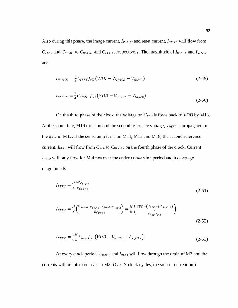
52 Also during this phase, the image current, IIMAGE and reset current, IRESET will flow from
CLEFT and CRIGHT to CBUCKL and CBUCKR respectively. The magnitude of IIMAGE and IRESET
are
𝐼𝐼𝐼𝐼𝐼𝐼𝐼𝐼𝐼𝐼𝑅𝑅 = 14𝐶𝐶𝐿𝐿𝑅𝑅𝐿𝐿𝑅𝑅𝑑𝑑𝑅𝑅𝑅𝑅𝑐𝑐 �𝑉𝑉𝐴𝐴𝐴𝐴 − 𝑉𝑉𝐼𝐼𝐼𝐼𝐼𝐼𝐼𝐼𝑅𝑅 − 𝑉𝑉𝑠𝑠ℎ ,𝐼𝐼5� (2-49)
𝐼𝐼𝑅𝑅𝑅𝑅𝑅𝑅𝑅𝑅𝑅𝑅 = 14𝐶𝐶𝑅𝑅𝐼𝐼𝐼𝐼𝐶𝐶𝑅𝑅𝑑𝑑𝑅𝑅𝑅𝑅𝑐𝑐 �𝑉𝑉𝐴𝐴𝐴𝐴 − 𝑉𝑉𝑅𝑅𝑅𝑅𝑅𝑅𝑅𝑅𝑅𝑅 − 𝑉𝑉𝑠𝑠ℎ ,𝐼𝐼8�
(2-50)
On the third phase of the clock, the voltage on CREF is force back to VDD by M13.
At the same time, M19 turns on and the second reference voltage, VREF2 is propagated to
the gate of M12. If the sense-amp turns on M11, M15 and M18, the second reference
current, IREF2 will flow from CREF to CBUCKR on the fourth phase of the clock. Current
IREF2 will only flow for M times over the entire conversion period and its average
magnitude is
𝐼𝐼𝑅𝑅𝑅𝑅𝐿𝐿2 = 𝐼𝐼𝑁𝑁
∆𝑉𝑉𝐶𝐶𝑅𝑅𝑅𝑅𝐿𝐿 2𝑅𝑅𝐶𝐶𝑅𝑅𝑅𝑅𝐿𝐿 2
(2-51)
𝐼𝐼𝑅𝑅𝑅𝑅𝐿𝐿2 = 𝐼𝐼𝑁𝑁�𝑉𝑉𝑠𝑠𝑅𝑅𝑠𝑠𝑠𝑠𝑠𝑠𝐶𝐶𝑅𝑅 ,𝐶𝐶𝑅𝑅𝑅𝑅𝐿𝐿 2−𝑉𝑉𝑑𝑑𝑠𝑠𝑅𝑅𝐶𝐶𝑅𝑅 ,𝐶𝐶𝑅𝑅𝑅𝑅𝐿𝐿 2
𝑅𝑅𝐶𝐶𝑅𝑅𝑅𝑅𝐿𝐿 2� = 𝐼𝐼
𝑁𝑁�𝑉𝑉𝐴𝐴𝐴𝐴−�𝑉𝑉𝑅𝑅𝑅𝑅𝐿𝐿 2+𝑉𝑉𝑠𝑠ℎ ,𝐼𝐼12�
4𝐶𝐶𝑅𝑅𝑅𝑅𝐿𝐿 𝑑𝑑𝑅𝑅𝑅𝑅𝑐𝑐
�
(2-52)
𝐼𝐼𝑅𝑅𝑅𝑅𝐿𝐿2 = 14𝐼𝐼𝑁𝑁𝐶𝐶𝑅𝑅𝑅𝑅𝐿𝐿𝑑𝑑𝑅𝑅𝑅𝑅𝑐𝑐 �𝑉𝑉𝐴𝐴𝐴𝐴 − 𝑉𝑉𝑅𝑅𝑅𝑅𝐿𝐿2 − 𝑉𝑉𝑠𝑠ℎ ,𝐼𝐼12� (2-53)
At every clock period, IIMAGE and IREF1 will flow through the drain of M7 and the
currents will be mirrored over to M8. Over N clock cycles, the sum of current into

53 CBUCKR is ideally zero and the digital relationship between the analog inputs signals with
respect to the reference signals is
𝐼𝐼𝐼𝐼𝐼𝐼𝑅𝑅𝑅𝑅𝑀𝑀𝑅𝑅 = 𝐼𝐼𝐼𝐼𝐼𝐼𝐼𝐼𝐼𝐼𝑅𝑅 + 𝐼𝐼𝑅𝑅𝑅𝑅𝐿𝐿1 (2-54)
𝐼𝐼𝑅𝑅𝑅𝑅𝑅𝑅𝑅𝑅𝑅𝑅 + 𝐼𝐼𝑅𝑅𝑅𝑅𝐿𝐿2 = 𝐼𝐼𝐼𝐼𝐼𝐼𝑅𝑅𝑅𝑅𝑀𝑀𝑅𝑅 = 𝐼𝐼𝐼𝐼𝐼𝐼𝐼𝐼𝐼𝐼𝑅𝑅 + 𝐼𝐼𝑅𝑅𝑅𝑅𝐿𝐿1 (2-55)
14𝐶𝐶𝑅𝑅𝐼𝐼𝐼𝐼𝐶𝐶𝑅𝑅𝑑𝑑𝑅𝑅𝑅𝑅𝑐𝑐 �𝑉𝑉𝐴𝐴𝐴𝐴 − 𝑉𝑉𝑅𝑅𝑅𝑅𝑅𝑅𝑅𝑅𝑅𝑅 − 𝑉𝑉𝑠𝑠ℎ ,𝐼𝐼8� + 1
4𝐼𝐼𝑁𝑁𝐶𝐶𝑅𝑅𝑅𝑅𝐿𝐿𝑑𝑑𝑅𝑅𝑅𝑅𝑐𝑐 �𝑉𝑉𝐴𝐴𝐴𝐴 − 𝑉𝑉𝑅𝑅𝑅𝑅𝐿𝐿2 − 𝑉𝑉𝑠𝑠ℎ ,𝐼𝐼12�
= 14𝐶𝐶𝐿𝐿𝑅𝑅𝐿𝐿𝑅𝑅𝑑𝑑𝑅𝑅𝑅𝑅𝑐𝑐 �𝑉𝑉𝐴𝐴𝐴𝐴 − 𝑉𝑉𝐼𝐼𝐼𝐼𝐼𝐼𝐼𝐼𝑅𝑅 − 𝑉𝑉𝑠𝑠ℎ ,𝐼𝐼5� + 1
4𝐼𝐼𝑁𝑁𝐶𝐶𝑅𝑅𝑅𝑅𝐿𝐿𝑑𝑑𝑅𝑅𝑅𝑅𝑐𝑐 �𝑉𝑉𝐴𝐴𝐴𝐴 − 𝑉𝑉𝑅𝑅𝑅𝑅𝐿𝐿1 − 𝑉𝑉𝑠𝑠ℎ ,𝐼𝐼12�
(2-56)
𝐼𝐼 = 𝑁𝑁 �𝐶𝐶𝐿𝐿𝑅𝑅𝐿𝐿𝑅𝑅 �𝑉𝑉𝐴𝐴𝐴𝐴−𝑉𝑉𝐼𝐼𝐼𝐼𝐼𝐼𝐼𝐼𝑅𝑅 −𝑉𝑉𝑠𝑠ℎ ,𝐼𝐼5�−𝐶𝐶𝑅𝑅𝐼𝐼𝐼𝐼𝐶𝐶𝑅𝑅 �𝑉𝑉𝐴𝐴𝐴𝐴−𝑉𝑉𝑅𝑅𝑅𝑅𝑅𝑅𝑅𝑅𝑅𝑅 −𝑉𝑉𝑠𝑠ℎ ,𝐼𝐼6�𝐶𝐶𝑅𝑅𝑅𝑅𝐿𝐿 (𝑉𝑉𝑅𝑅𝑅𝑅𝐿𝐿 1−𝑉𝑉𝑅𝑅𝑅𝑅𝐿𝐿 2)
� (2-57)
The transfer function for this DSM shows that it is robust to any gain error cause
by voltage threshold mismatch. This is because the denominator of the transfer function
does not contain the voltage threshold of any transistor in the DSM. The gain of the DSM
is controlled by the two reference voltage signals, VREF1 and VREF2. The difference
between VREF1 and VREF2 determines the gain of the DSM.
However, this DSM is still prone to offset error as the nominator of the transfer
function contains the voltage threshold of M5 and M6. Path switching methodology can
be applied to this DSM to reduce the effects of offset error. Figure 2.18 illustrates the
DSM with reference path, input path switching and gain error correction.

54
Figure 2.18 Schematic of a CMOS Imager Delta Sigma Modulator with reference
path, input path switching and gain error correction.
Just like conversion method discussed in Chapter 2.5, conversion period is now
divided into 2 equal halves where each half is N/2 clock cycles long. On the first half of
the conversion period, the control signals SLT and SLB are set to VDD and VSS
respectively. For this half of the conversion period, the digital code representation of the
analog input signals with respect to the two reference input signals, Mt=1 is
𝐼𝐼𝑠𝑠=1 = 𝑁𝑁2�𝐶𝐶𝐿𝐿𝑅𝑅𝐿𝐿𝑅𝑅 �𝑉𝑉𝐴𝐴𝐴𝐴−𝑉𝑉𝐼𝐼𝐼𝐼𝐼𝐼𝐼𝐼𝑅𝑅 −𝑉𝑉𝑠𝑠ℎ ,𝐼𝐼5�−𝐶𝐶𝑅𝑅𝐼𝐼𝐼𝐼𝐶𝐶𝑅𝑅 �𝑉𝑉𝐴𝐴𝐴𝐴−𝑉𝑉𝑅𝑅𝑅𝑅𝑅𝑅𝑅𝑅𝑅𝑅 −𝑉𝑉𝑠𝑠ℎ ,𝐼𝐼6�
𝐶𝐶𝑅𝑅𝑅𝑅𝐿𝐿 (𝑉𝑉𝑅𝑅𝑅𝑅𝐿𝐿 1−𝑉𝑉𝑅𝑅𝑅𝑅𝐿𝐿 2) � (2-58)

55
On last half of the conversion period, the control signals SLT and SLB are now
set to VSS and VDD respectively. The digital code representation of the analog input
signals with respect to the two reference input signals for the last half of the sensing
period, Mt=2 is
𝐼𝐼𝑠𝑠=2 = 𝑁𝑁2�𝐶𝐶𝐿𝐿𝑅𝑅𝐿𝐿𝑅𝑅 �𝑉𝑉𝐴𝐴𝐴𝐴−𝑉𝑉𝐼𝐼𝐼𝐼𝐼𝐼𝐼𝐼𝑅𝑅 −𝑉𝑉𝑠𝑠ℎ ,𝐼𝐼6�−𝐶𝐶𝑅𝑅𝐼𝐼𝐼𝐼𝐶𝐶𝑅𝑅 �𝑉𝑉𝐴𝐴𝐴𝐴−𝑉𝑉𝑅𝑅𝑅𝑅𝑅𝑅𝑅𝑅𝑅𝑅 −𝑉𝑉𝑠𝑠ℎ ,𝐼𝐼5�
𝐶𝐶𝑅𝑅𝑅𝑅𝐿𝐿 (𝑉𝑉𝑅𝑅𝑅𝑅𝐿𝐿 1−𝑉𝑉𝑅𝑅𝑅𝑅𝐿𝐿 2) � (2-59)
Similarly, the digital code representation from the 2 halves are added together at
the end of the conversion period to receive the final digital output code of the DSM with
both gain and offset correction. Its final digital output code is
𝐼𝐼 = 𝐼𝐼𝑠𝑠=1 + 𝐼𝐼𝑠𝑠=2 = 𝑁𝑁2�(𝐶𝐶𝐿𝐿𝑅𝑅𝐿𝐿𝑅𝑅 +𝐶𝐶𝑅𝑅𝐼𝐼𝐼𝐼𝐶𝐶𝑅𝑅 )
𝐶𝐶𝑅𝑅𝑅𝑅𝐿𝐿 (𝑉𝑉𝑅𝑅−𝑉𝑉𝐼𝐼)
(𝑉𝑉𝑅𝑅𝑅𝑅𝐿𝐿 1−𝑉𝑉𝑅𝑅𝑅𝑅𝐿𝐿 2)� (2-60)
The input-output transfer function for this DSM does not include the voltage
threshold of any transistor in the DSM. This means that the DSM is robust to any offset
or gain error cause by voltage threshold mismatches. However, a gain error might still
occur if the capacitor ratio between the sum of CLEFT and CRIGHT and CREF is not identical
between the many DSMs in the array.
The least significant bit voltage, VLSB for this DSM is specified in Equation 2-61
seen below. The bit accuracy of the conversion increases linearly with the number of
clock cycles, N during the conversion period.
𝑉𝑉𝐿𝐿𝑅𝑅𝐿𝐿 = 2𝑁𝑁� 𝐶𝐶𝑅𝑅𝑅𝑅𝐿𝐿
(𝐶𝐶𝐿𝐿𝑅𝑅𝐿𝐿𝑅𝑅 +𝐶𝐶𝑅𝑅𝐼𝐼𝐼𝐼𝐶𝐶𝑅𝑅 )� (𝑉𝑉𝑅𝑅𝑅𝑅𝐿𝐿1 − 𝑉𝑉𝑅𝑅𝑅𝑅𝐿𝐿2) (2-61)

56 In addition, the input dynamic range is given by Equation 2-62. The input
dynamic range can be accurately controlled by the reference voltage signals, VREF1 and
VREF2. In low light environment, the dynamic range of the input signals is reduced. If a
gain stage is not used to amplify the input signals, the image decoded will be dark. This
DSM can compensate for this reduction of the input dynamic range without using a gain
stage. This is can be accomplished by reducing the delta between VREF1 and VREF2. On the
other hand in a bright light environment, the DSM can compensate for the increase in
input dynamic range by increasing the delta between VREF1 and VREF2.
𝐼𝐼𝐴𝐴𝐶𝐶 𝑠𝑠𝑅𝑅𝑝𝑝𝑅𝑅𝑠𝑠 𝑒𝑒𝐶𝐶𝑅𝑅𝑔𝑔𝑒𝑒 = �(𝐶𝐶𝐿𝐿𝑅𝑅𝐿𝐿𝑅𝑅 +𝐶𝐶𝑅𝑅𝐼𝐼𝐼𝐼𝐶𝐶𝑅𝑅 )𝐶𝐶𝑅𝑅𝑅𝑅𝐿𝐿
� 1(𝑉𝑉𝑅𝑅𝑅𝑅𝐿𝐿 1−𝑉𝑉𝑅𝑅𝑅𝑅𝐿𝐿 2)
(2-62)

57
CHAPTER 3: SIMULATION RESULTS AND TEST CHIP INFORMATION
3.1 Simulation Results
A voltage source is added in series with the gate of a transistor to simulate a
variation in its threshold voltage. For all the simulations ran in this chapter, N is 512,
VDD is 5V, VSS is 0V, VREF1 is 3.5V, VREF2 is 2.25V, VR is 3.5V and VI is decrease from
3.5V to 1V. This will yield a input dynamic range of 2.5V. The frequency of the master
clock is 10MHz.
Figure 3.1 shows the simulation result for the DSM with just the reference path,
like in Figure 2.11. This DSM is prone to offset and gain error if voltage threshold
mismatch exists between the many DSMs in the array.
The red line in Figure 3.1 is the transfer function of the DSM when a negative
0.25V voltage offset is applied to the gate of M5. The transfer function of the DSM shift
upwards from ideal and this is known as offset error. If a positive voltage offset is applied
to the gate of M5, the transfer function will move downwards from ideal instead. On the
other hand, the green line is the transfer function of the DSM when a negative 0.2V
offset is applied to the gate of M12 and this is gain error. A negative voltage offset will
reduce the slope of the transfer function and a positive voltage offset will increase the
slope.

58
Figure 3.1 Simulation Results for the CMOS Imager DSM with reference path.
Different voltage offsets were applied to the gate of M12 and M5 to simulate offset
and gain error.
The DSM with reference path and gain error correction like in Figure 2.15 should
be robust to gain error cause by voltage threshold mismatch. Figure 3.2 shows simulation
results of the DSM with reference path and gain error correction. A negative or positive
0.2V voltage offset on M12 does not reduce or increase the slope of the transfer function.
However, offset error still occurs if a voltage threshold offset exists on M5, as shown as
the purple line in Figure 3.2.
0
100
200
300
400
500
600
0 0.5 1 1.5 2 2.5 3
M
Count
VRESET - VSIGNAL (V)
DSM with reference path
M12 offset = 0V, M5 offset = 0V, ideal
M12 offset = 0V, M5 offset = -0.25V
M12 offset = -0.2V, M5 offset = 0V

59
Figure 3.2 Simulation Results for the CMOS Imager DSM with reference path and
gain error correction. Different voltage offsets were applied to the gate of M12 and
M5 to simulate offset and gain error.
A DSM with reference path, input path switching and gain error correction should
be robust to both offset and gain error cause by voltage threshold mismatch. Multiple
simulations were run on the DSM in Figure 2.18 and its results are shown in Figure 3.3.
A 0.25V voltage offset on M5 does not shift the transfer function downward and the
transfer function tracks the ideal transfer function except on the front and tail end. The
transfer function curves upward at the front end and curves downward at the tail end.
This magnitude of the deviation from the ideal line is equivalent to the digital code
representation of the offset value, 0.25V. This means any input signal that fall on either
0
100
200
300
400
500
600
0 0.5 1 1.5 2 2.5 3
M
Count
VRESET - VSIGNAL (V)
DSM with reference path and gain error correction
M12 offset = -0.2V, M5 offset = 0V
M12 offset = 0V, M5 offset = 0V, ideal
M12 offset = +0.2V, M5 offset = 0V
M12 offset = 0V, M5 offset = 0.25V

60 curve, will produce an erroneous digital code representation. Therefore, the input
dynamic range of the DSM is reduced by twice the voltage threshold offset on M5. A
DSM with voltage offsets on both M5 and M12 will have a similar transfer function as
the DSM with voltage offsets on only M5, as shown in Figure 3.4.
Figure 3.3 Simulation Results for the CMOS Imager DSM with reference path,
input path switching, and gain error correction. A 0.25V voltage offsets was applied
to the gate of M5 to simulate offset error.
0
100
200
300
400
500
600
0 0.5 1 1.5 2 2.5 3
M
Count
VRESET - VSIGNAL (V)
DSM with reference path, input path switching and gain error correction
M12 offset = 0V, M5 offset = 0.25V
M12 offset = 0V, M5 offset = 0V

61
Figure 3.4 Simulation Results for the CMOS Imager DSM with reference path,
input path switching, and gain error correction. Different voltages offsets were
applied to M5 and M12 to simulate offset and gain error.
0
100
200
300
400
500
600
0 0.5 1 1.5 2 2.5 3
M
Count
VRESET - VSIGNAL (V)
DSM with reference path, input path switching and gain error correction
M12 offset = 0V, M5 offset = 0.25V
M12 offset = -0.2V, M5 offset = 0.25V

62
3.2 Layout
The test chip consists of the DSM in Figure 2.11, 2.14, 2.15 and 2.18 . The
standalone sense-amp and 4 phase non-overlapping clock generator (Figure 2.16) were
also included in the layout for direct testing.
Figure 3.5 Test chip full layout

63 3.3 General Test Chip Information
Figure 3.6 Bonding diagram for test chip provided by MOSIS.

64
Table 3.5 Pin Description
Pin Number Pin Type Pin Description
1,12,14,17,23,36 Supply
VSS Supply. There are separate VSS signals for the multiple DSM ADCs, sense-amp, 4-phase nonoverlapping clock generator, and output drivers.
2,8,15,16,24,25 Supply
VDD Supply. There are separate VDD signals for the multiple DSM ADCs, sense-amp, 4-phase nonoverlapping clock generator, and output drivers.
3,4,5,21,22 Input The different DSM ADCs input reference signals.6,7,39,40 Input The path control signals for the DSM ADCs.19,37 Input The input image signals for the DSM ADCs.20,38 Input The input reset signals for the DSM ADCs.
18 Input The clock input signal for the multiple DSMs, sense-amp, and 4-phase nonoverlapping clock generator
27,28,29,30 OutputThe output of the 4 phase non-overlapping clock generator
10,11 Output The output of the sense-amp9,13,26,31,32,33,34,35 Output The output of the multiple DSM ADCs

65
CHAPTER 4: CONCLUSION AND FUTURE WORK
4.1 Conclusion
A CMOS image sensor using a per-column DSM ADC has many advantageous
over a pipeline ADC. However, transistor voltage threshold mismatches between the
many DSMs in the array causes offset and gain error in its transfer. These errors will lead
to fixed pattern noise. A complex digital signal processor is needed if correction is to be
done in the digital domain. A DSM ADC with offset error correction was introduced by
Montierth to help reduce some of this error. To remove both gain and offset error cause
by transistor voltage threshold mismatch, a new DSM ADC architecture was proposed in
this Thesis.
The bit accuracy of a pipeline ADC is fixed by design and cannot be increased
without a complete redesign. The DSM ADC bit accuracy is proportional to the number
of clock cycles during the sensing period. A minimum of 1024 clock cycles is needed if a
10-bit conversion accuracy is required. On the other hand, a conversion period of 4096
clock cycles is required for a 12-bit conversion accuracy. Increasing the bit accuracy on a
DSM ADC is easy and does not require a major redesign.
A pipeline ADC will require a separate gain stage to increase or reduce the input
dynamic range. This extra gain stage requires additional power and layout area. The per-
column DSM ADC is able to reduce or increase the input dynamic range by simply

66 controlling the delta between the two reference signals, VREF1 and VREF2. A large delta
between the two reference signals indicates a large input dynamic range and vice-versa.
4.2 Future Work
As noted previously, the conversion period of the DSM ADC is proportional to
the conversion bit accuracy. A very long conversion period may not be desirable. The
charge stored on the sample and hold capacitors will leak over time and conversion errors
may appear if the voltage on the sample and hold capacitor deviates from its original
sampled voltages. Therefore, introducing a topology to increase the sampling rate of the
DSM may be a topic for future work. One method may be to introduce a parallel K-path
sampling of the DSM. The DSM with parallel K-path sampling will sample the voltage
on net_buckL and net_buckR for K extra times at every clock period. The length of the
entire conversion period is N/K clock cycles instead.
The DSM ADC proposed in this Thesis only removes offset and gain error cause
by transistor voltage threshold mismatches. However, if a capacitor ratio mismatch
occurs between the sum of CLEFT and CRIGHT and CREF, a gain error might still occur. A
topology to reduce the effect of gain error from capacitance ratio mismatch may also be
another topic for future work.

67
REFERENCES
[1] Dennis Glen Montierth, Using Delta-Sigma Modulation for Sensing in a CMOS Imager, thesis (M.Sc), Boise State University, 2008
[2] Baker, R. Jacob, CMOS Circuit Design, Layout and Simulation, 2nd Edition, IEEE press, 2005, ISBN 0-471-70055-X
[3] Eric R. Fossum, “CMOS Image Sensors: Electronic Camera-On-A-Chip”, IEEE Transactions on Electron Devices, Vol. 44, No. 10, pp. 1689-1698, October 1997.
[4] Noble, P.J.W, “Self-scanned silicon image detector arrays”, IEEE Transactions, Vol. 15, No. 4, pp. 202-209, April 1968.
[5] D. James, L. Klibanov, G. Tompkins, St. J. Dixon-Warren, Inside CMOS Imager Sensor Technology, Retrieved June 1, 2009, from www.chipworks.com.tw/resources/whitepapers/Inside-CMOS.pdf.
[6] John Coghill, DALSA Corp, 2003, Digital Imaging Technology 101, Retrieved May 31, 2009, from https://classes.yale.edu/04- 05/enas627b/lectures/EENG427l07DigitalImaging.pdf