g240hw01 v0 24' auo au optronics industrial lcd … shipping label (on the rear side of tft-lcd...
TRANSCRIPT

AU OPTRONICS CORPORATION Product Specification
document version 1.1 1
G240HW01 V0
Preliminary Specification Final Specification
Module 24.0” Color TFT-LCD Model Name G240HW01 V0
Customer Date
Checked & Approved by
Note: This Specification is subject to change without notice.
Approved by Date
Vito Huang 2012/03/22
Prepared by
Jimmy Tsai 2012/03/22
General Display Business Division / AU Optronics corporation
Provided by www.display-solution.com [email protected]

AU OPTRONICS CORPORATION Product Specification
document version 1.1 2
G240HW01 V0
Contents
1. Operating Precautions..................................................................................... 42. General Description......................................................................................... 5
2.1 Display Characteristics ..........................................................................................................52.2 Optical Characteristics ...........................................................................................................6
3. Functional Block Diagram............................................................................... 94. Absolute Maximum Ratings .......................................................................... 10
4.1 TFT LCD Module..................................................................................................................104.2 Backlight Unit .......................................................................................................................104.3 Absolute Ratings of Environment ........................................................................................10
5. Electrical Characteristics .............................................................................. 115.1 TFT LCD Module.................................................................................................................. 115.2 Backlight Unit .......................................................................................................................13
6. Signal Characteristic ..................................................................................... 146.1 Pixel Format Image..............................................................................................................146.2 Signal Description ................................................................................................................156.3 The Input Data Format.........................................................................................................166.4 Interface Timing....................................................................................................................176.5 Power ON/OFF Sequence...................................................................................................18
7. Connector & Pin Assignment........................................................................ 197.1 TFT LCD Module: LVDS Connector ....................................................................................197.2 Backlight Unit: LED Connector ............................................................................................20
8. Reliability Test ............................................................................................... 219. Mechanical Characteristics........................................................................... 2210. Label and Packaging ................................................................................... 24
10.1 Shipping Label (on the rear side of TFT-LCD display)......................................................2410.2 Carton Package .................................................................................................................24
11. Safety............................................................................................................ 2511.1 Sharp Edge Requirements ................................................................................................2511.2 Materials .............................................................................................................................2511.3 Capacitors ..........................................................................................................................2511.4 National Test Lab Requirement .........................................................................................25
Provided by www.display-solution.com [email protected]

AU OPTRONICS CORPORATION Product Specification
document version 1.1 3
G240HW01 V0
Record of Revision
Version and Date Page Old description New Description Remark0.1 2011/02/15 All First Edition for Customer All 0.2 2011/03/10 13 Add
0.3 2011/05/11 22 Old drawing Update to new one (adding 3 ribs)
0.4 2011/06/13 5 Contrast ratio: 3,000 : 1 Contrast ratio: 5,000 : 1 6
5 0.5 2011/07/07 23 Back bezel has three ribs Update drawing 1.0 2011/12/12 5 Power= 36.3 W 30 W
6 IF= 120mA IF= 100mA
13
1.1 2012/03/22 24
Provided by www.display-solution.com [email protected]

AU OPTRONICS CORPORATION Product Specification
document version 1.1 4
G240HW01 V0
1. Operating Precautions1) Since front polarizer is easily damaged, pay attention not to scratch it.2) Be sure to turn off power supply when inserting or disconnecting from input connector.3) Wipe off water drop immediately. Long contact with water may cause discoloration or spots.4) When the panel surface is soiled, wipe it with absorbent cotton or other soft cloth.5) Since the panel is made of glass, it may break or crack if dropped or bumped on hard surface.6) Since CMOS LSI is used in this module, take care of static electricity and insure human earth when handling.7) Do not open or modify the Module Assembly.8) In case if a Module has to be put back into the packing container slot after once it was taken out from the
container, take it easily, or the TFT Module may be damaged.9) At the insertion or removal of the Signal Interface Connector, be sure not to rotate nor tilt the Interface
Connector of the TFT Module.10) After installation of the TFT Module into an enclosure, do not twist nor bend the TFT Module even momentary.
At designing the enclosure, it should be taken into consideration that no bending/twisting forces are applied tothe TFT Module from outside. Otherwise the TFT Module may be damaged.
11) Small amount of materials having no flammability grade is used in the LCD module. The LCD module shouldbe supplied by power complied with requirements of Limited Power Source (IEC60950 or UL1950), or beapplied exemption.
12) Severe temperature condition may result in different luminance, response time and LED life time.13) The data on this specification sheet is applicable when LCD module is placed in landscape position.14) Continuous displaying fixed pattern may induce image sticking. It is recommended to use screen saver or
shuffle content periodically if fixed pattern is displayed on the screen.
Provided by www.display-solution.com [email protected]

AU OPTRONICS CORPORATION Product Specification
document version 1.1 5
G240HW01 V0
2. General DescriptionThis specification applies to the 24 inch-wide Color TFT-LCD Module G240HW01 V0. The display supports the Full HD - 1920(H) x 1080(V) screen format and 16.7M colors (RGB 8-bits data). All input signals are dual channel LVDS interface. LED driver board is included. G240HW01 V0 is designed for industrial display applications.
2.1 Display Characteristics The following items are characteristics summary on the table under 25 condition:
ITEMS Unit SPECIFICATIONS Screen Diagonal [mm] 609.7(24.0”) Active Area [mm] 531.36 (H) x 298.89 (V)Pixels H x V 192 0(x3) x 1080 Pixel Pitch [um] 276.75 (per one triad) ×276.75Pixel Arrangement R.G.B. Vertical StripeDisplay Mode VA Mode, Normally BlackWhite Luminance ( Center ) [cd/m2] 300 Contrast Ratio 5000: 1 Optical Response Time [msec] 25 Nominal Input Voltage VDD [Volt] +5.0 V Power Consumption [Watt] 30 Weight [g] 2300 (typical) Physical Size [mm] 556.0 (W) x 323.2 (H) x 17.0 (D) Electrical Interface Dual channel LVDS Support Color 16.7M colors (true 8-bit) Surface Treatment Anti-Glare, 3H Temperature Range
Operating Storage (Shipping)
[oC] [oC]
0 to +50 -20 to +60
RoHS Compliance RoHS Compliance
Provided by www.display-solution.com [email protected]

AU OPTRONICS CORPORATION Product Specification
document version 1.1 6
G240HW01 V0
2.2 Optical Characteristics The optical characteristics are measured under stable conditions at 25 (Room Temperature):
Item Unit Conditions Min. Typ. Max. Note White Luminance [cd/m2] IF= 100mA 240 300 - 1
Uniformity % 9 Points 75 80 - 1, 2, 3
Contrast Ratio 3000 5000 - 4 Cross talk % - - 1.5 5
Rising - 16 - Falling - 9 - Response Time [msec] Rising + Falling - 25 -
6
[degree] [degree]
Horizontal (Right) CR = 10 (Left)
75 75
89 89
- - Viewing Angle
[degree] [degree]
Vertical (Upper) CR = 10 (Lower)
75 75
89 89
- -
7
Red x 0.593 0.643 0.693 Red y 0.289 0.339 0.389 Green x 0.279 0.329 0.379 Green y 0.574 0.624 0.674 Blue x 0.105 0.155 0.205 Blue y 0.000 0.048 0.098 White x 0.263 0.313 0.363
Color / Chromaticity Coordinates (CIE 1931)
White y 0.279 0.329 0.379 Color Gamut % 69 -
Note 1: Measurement method Equipment Pattern Generator, Power Supply, Digital Voltmeter, Luminance meter (SR_3 or equivalent)
Aperture 1with50cmviewingdistance Test Point Center Environment < 1 lux
LCD Module SR_3 or equivalent
Measuring distance
Module Driving Equipment
Provided by www.display-solution.com [email protected]

AU OPTRONICS CORPORATION Product Specification
document version 1.1 7
G240HW01 V0
Note 2: Definition of 9 points position. Display active area:
Note 3: The luminance uniformity of 9 points is defined by dividing the minimum luminance values by the maximum test point luminance
Note 4: Definition of contrast ratio (CR):
Note 5: Definition of cross talk (CT)
CT = | YB – YA | / YA × 100 (%) Where YA = Luminance of measured location without gray level 255 pattern (cd/m2) YB = Luminance of measured location with gray level 255 pattern (cd/m2)
Minimum Brightness of nine points δW9 = Maximum Brightness of nine points
Contrast ratio (CR)= Brightness on the “White” stateBrightness on the “Black” state
50 %
90 %
90 % 50 %
10 %
10 %
1/2
1/2
1/6
1/6 A
B
1/2
1/2
1/6
1/6
2/3 1/3
1/3
2/3
A’
B’
127 gray level 127 gray level
255 gray level
Provided by www.display-solution.com [email protected]

AU OPTRONICS CORPORATION Product Specification
document version 1.1 8
G240HW01 V0
Note 6: Definition of response time:
The output signals of photo detector are measured when the input signals are changed from “White” to “Black” (falling time) and from “Black” to “White” (rising time), respectively. The response time interval is between 10% and 90% of amplitudes. Please refer to the figure as below.
Note 7: Definition of viewing angle Viewingangleisthemeasurementofcontrastratio$10,atthescreencenter,overa180°horizontaland180°verticalrange (off-normal viewing angles). The 180° viewing angle range is broken down as below: 90° (θ) horizontal left and right, and 90° (Φ) vertical high (up) and low (down). The measurement direction is typically perpendicular to the display surface with the screen rotated to its center to develop the desired measurement viewing angle.
10090
100
%
Opticalresponse
White Black White
Tf Tr
90
100
Opticalresponse
White Black White
Tr
Provided by www.display-solution.com [email protected]

AU OPTRONICS CORPORATION Product Specification
document version 1.1 9
G240HW01 V0
3. Functional Block DiagramThe following diagram shows the functional block of the 24 inches wide Color TFT-LCD Module:
LVDS Connector: JAE (FI-XB30SRL-HF11) or equivalent. LED Connector: Sin Sheng (MS24049HJ) or equivalent.
Connector
DC/DC Converter
LVDS Receiver
Timing Controller
Gamma Correction
TFT-LCD 1920*(3)*1080
Pixels
G1
G1080
D1 D5760
LED driver board DC POWER
AUO ASIC
LVDS
70 LEDs
I/F + X-PCB
X-Driver IC
Y-Driver IC
+5V
Provided by www.display-solution.com [email protected]

AU OPTRONICS CORPORATION Product Specification
document version 1.1 10
G240HW01 V0
4. Absolute Maximum Ratings4.1 TFT LCD Module
4.2 Backlight Unit Item Symbol Min Max Unit Conditions
LED Input Voltage Vcc 10.8 13.2 [Volt] Note 1,2
4.3 Absolute Ratings of Environment Item Symbol Min. Max. Unit Conditions
Operating Temperature TOP 0 +50 [oC] Operation Humidity HOP 5 90 [%RH] Storage Temperature TST -20 +60 [oC] Storage Humidity HST 5 90 [%RH]
Note 3
Note 1: With in Ta (25) Note 2: Permanent damage to the device may occur if exceeding maximum values Note 3: For quality perfermance, please refer to AUO IIS(Incoming Inspection Standard).
Operating Range Storage Range
Item Symbol Min Max Unit ConditionsLogic/LCD Drive Voltage VDD 0 6.0 [Volt] Note 1,2
Provided by www.display-solution.com [email protected]

AU OPTRONICS CORPORATION Product Specification
document version 1.1 11
G240HW01 V0
5. Electrical Characteristics5.1 TFT LCD Module 5.1.1 Power Specification
Symbol Parameter Min Typ Max Units Remark VDD Logic/LCD Drive
Voltage 4.5 5.0 5.5 [Volt] ±10%
IDD VDD Current - 900 1200 [mA] VDD= 5.0V, All White Pattern At 60Hz
Irush LCD Inrush Current - - 3 [A] Note 1
PDD VDD Power - 4.5 6 [Watt]VDD= 5.0V, All White Pattern At 60Hz
Note 1: Measurement condition: +5.0V
+12.0V
VCC
R147K
R2
1K
VR147K
SW1SW MAG-SPST
12
F1
Q3AO6402
G
D2
SD1
D5
D6
C11uF/16V
Q3AO6402
G
D2 SD1
D5D6
C3
0.01uF/25V
C21uF/25V
(High to Low)ControlSignal
(LCD Module Input)
90%
10%VDD rising time 0V
5.0V
0.5ms
Provided by www.display-solution.com [email protected]

AU OPTRONICS CORPORATION Product Specification
document version 1.1 12
G240HW01 V0
5.1.2 Signal Electrical Characteristics Input signals shall be low or Hi-Z state when VDD is off.
Note: LVDS Signal Waveform.
Symbol Item Min. Typ. Max. Unit Remark
VTH Differential Input High Threshold - - 100 [mV] VCM=1.2V
VTL Differential Input Low Threshold -100 - - [mV] VCM=1.2V
VID Input Differential Voltage 100 400 600 [mV]
VICM Differential Input Common Mode Voltage 0.3 - 1.25 [V] VTH/VTL=±100mV
VTH VID
VICM
VSS
Provided by www.display-solution.com [email protected]

AU OPTRONICS CORPORATION Product Specification
document version 1.1 13
G240HW01 V0
5.2 Backlight Unit 5.2.1 LED Driver Following characteristics are measured under stableconditionat25:(RoomTemperature).
Symbol Parameter Min Typ Max Unit Remark Vcc Input Voltage 10.8 12 13.2 Volt Ivcc Input Current - 2.0 - A 100% Dimming PLED Power Consumption - 24 - Watt 100% Dimming, Note3 FPWM PWM Dimming Frequency 200 - 20k Hz
Swing Voltage 0 3.3 3.6 Volt Dimming Duty Cycle 10 - 100 %
Vanalog Analog Dimming Voltage - N/A - No Analog Dimming IF LED Forward Current - 100 - mA Ta = 25oC
Operating Life 50000 - - Hrs Ta = 25oC
Note 1: Ta means ambient temperature of TFT-LCD module, Note 2: If module is driven by high current or at high ambient temperature & humidity condition. The operating life will be
reduced. Note 3: LED light bar structure: ( 7 strings x 10pcs / string =70pcs LED) Note 4: Operating life means brightness goes down to 50% initial brightness. Typical operating life time is estimated data.
Provided by www.display-solution.com [email protected]
AU OPTRONICS CORPORATION Product Specification
document version 1.1 14
G240HW01 V0
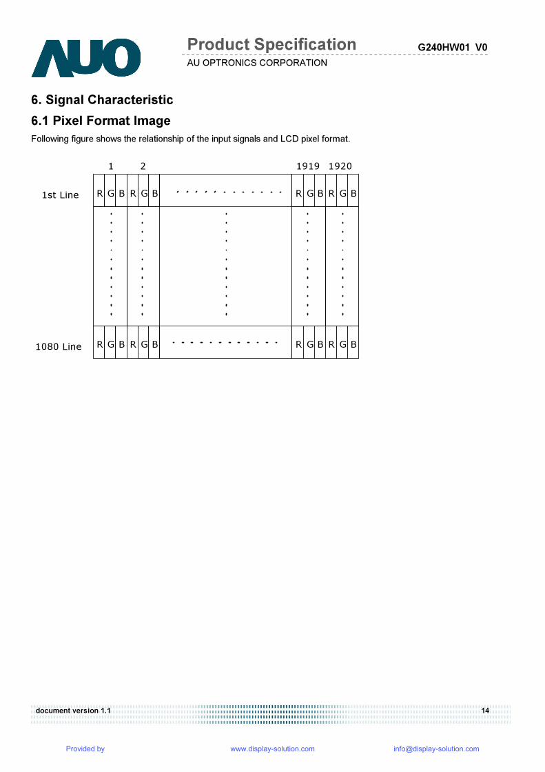
6. Signal Characteristic6.1 Pixel Format Image Following figure shows the relationship of the input signals and LCD pixel format.
R G B R G B
R G B R G B
R G B R G B
R G B R G B
1 2 1919 1920
1st Line
1080 Line
Provided by www.display-solution.com [email protected]

AU OPTRONICS CORPORATION Product Specification
document version 1.1 15
G240HW01 V0
6.2 Signal DescriptionThe module using a pair of LVDS receiver SN75LVDS82(Texas Instruments) or compatible. LVDS is a differential signal technology for LCD interface and high speed data transfer device. Transmitter shall be SN75LVDS83(negative edge sampling) or compatible. The first LVDS port(RxOxxx) transmits odd pixels while the second LVDS port(RxExxx) transmits even pixels.
PIN # SIGNAL NAME DESCRIPTION 1 RXinO0- Negative LVDS differential data input (Odd data) 2 RXinO0+ Positive LVDS differential data input (Odd data) 3 RXinO1- Negative LVDS differential data input (Odd data) 4 RXinO1+ Positive LVDS differential data input (Odd data) 5 RXinO2- Negative LVDS differential data input (Odd data, H-Sync, V-Sync, DSPTMG) 6 RXinO2+ Positive LVDS differential data input (Odd data, H-Sync, V-Sync, DSPTMG) 7 GND Power Ground 8 RxOCLKIN- Negative LVDS differential clock input (Odd clock) 9 RxOCLKIN+ Positive LVDS differential clock input (Odd clock) 10 RXinO3- Negative LVDS differential data input (Odd data) 11 RXinO3+ Positive LVDS differential data input (Odd data) 12 RXinE0- Negative LVDS differential data input (Even data) 13 RXinE0+ Positive LVDS differential data input (Even data) 14 GND Power Ground 15 RXinE1- Positive LVDS differential data input (Even data) 16 RXinE1+ Negative LVDS differential data input (Even data) 17 GND Power Ground 18 RXinE2- Negative LVDS differential data input (Even data) 19 RXinE2+ Positive LVDS differential data input (Even data) 20 RxECLKIN- Negative LVDS differential clock input (Even clock) 21 RxECLKIN+ Positive LVDS differential clock input (Even clock) 22 RXinE3- Negative LVDS differential data input (Even data) 23 RXinE3+ Positive LVDS differential data input (Even data) 24 GND Power Ground 25 NC No contact (For AUO test only) 26 NC No contact (For AUO test only) 27 VDD Power +5V 28 VDD Power +5V 29 VDD Power +5V 30 VDD Power +5V
Provided by www.display-solution.com [email protected]

AU OPTRONICS CORPORATION Product Specification
document version 1.1 16
G240HW01 V0
6.3 The Input Data Format
Note1: 8-bits signal input. Note2: L:NS alike H:Thine alike
Provided by www.display-solution.com [email protected]
AU OPTRONICS CORPORATION Product Specification
document version 1.1 17
G240HW01 V0
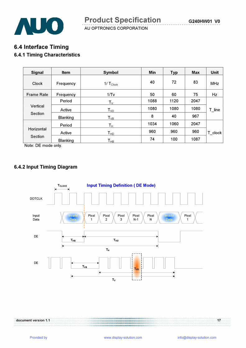
6.4 Interface Timing 6.4.1 Timing Characteristics
Signal Item Symbol Min Typ Max Unit
Clock Frequency 1/ TClock 40 72 83 MHz
Frame Rate Frequency 1/Tv 50 60 75 Hz Period TV 1088 1120 2047 Active TVD 1080 1080 1080 Vertical
Section Blanking TVB 8 40 967
T_line
Period TH 1034 1060 2047 Active THD 960 960 960 Horizontal
Section Blanking THB 74 100 1087
T_clock
Note: DE mode only.
6.4.2 Input Timing Diagram
DOTCLK
DE
TH
THB THD
DE
TV
TVB TVD
Input Timing Definition ( DE Mode)TCLOCK
InputData
Pixel1
Pixel2
Pixel3
PixelN-1
PixelN
InvaildData
InvaildData
Pixel1
Provided by www.display-solution.com [email protected]
AU OPTRONICS CORPORATION Product Specification
document version 1.1 18
G240HW01 V0
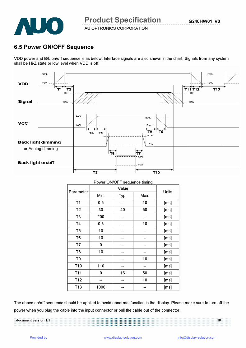
6.5 Power ON/OFF Sequence VDD power and B/L on/off sequence is as below. Interface signals are also shown in the chart. Signals from any system shall be Hi-Z state or low level when VDD is off.
Power ON/OFF sequence timing Value Parameter Min. Typ. Max. Units
T1 0.5 -- 10 [ms] T2 30 40 50 [ms] T3 200 -- -- [ms] T4 0.5 -- 10 [ms] T5 10 -- -- [ms] T6 10 -- -- [ms] T7 0 -- -- [ms] T8 10 -- -- [ms] T9 -- -- 10 [ms] T10 110 -- -- [ms] T11 0 16 50 [ms] T12 -- -- 10 [ms] T13 1000 -- -- [ms]
The above on/off sequence should be applied to avoid abnormal function in the display. Please make sure to turn off the power when you plug the cable into the input connector or pull the cable out of the connector.
or Analog dimming
Provided by www.display-solution.com [email protected]

AU OPTRONICS CORPORATION Product Specification
document version 1.1 19
G240HW01 V0
7. Connector & Pin AssignmentPhysical interface is described as for the connector on module. These connectors are capable of accommodating the following signals and will be following components.
7.1 TFT LCD Module: LVDS Connector
Connector Name / Designation Interface Connector / Interface card Manufacturer JAE or compatible
Type Part Number JAE (FI-XB30SRL-HF11) or equivalent.
Mating Housing Part Number FI-X30HL (JAE) or compatible
Pin# Signal Name Pin# Signal Name 1 RxOIN0- 2 RxOIN0+ 3 RxOIN1- 4 RxOIN1+ 5 RxOIN2- 6 RxOIN2+ 7 GND 8 RxOCLKIN- 9 RxOCLKIN+ 10 RxOIN3- 11 RxOIN3+ 12 RxEIN0- 13 RxEIN0+ 14 GND 15 RxEIN1- 16 RxEIN1+ 17 GND 18 RxEIN2- 19 RxEIN2+ 20 RxECLKIN- 21 RxECLKIN+ 22 RxEIN3- 23 RxEIN3+ 24 GND 25 NC 26 NC 27 VDD 28 VDD 29 VDD 30 VDD
Provided by www.display-solution.com [email protected]

AU OPTRONICS CORPORATION Product Specification
document version 1.1 20
G240HW01 V0
7.2 Backlight Unit: LED Connector
Connector Name / Designation LED Connector Manufacturer Sin Sheng or compatible Connector Model Number MS24049HJ Mating Model Number 2404PS-2 or compatible
PIN # SIGNAL NAME DESCRIPTION 1 V12 Input voltage, 12V 2 V12 Input voltage, 12V 3 V12 Input voltage, 12V 4 --- NC 5 GND Ground 6 GND Ground 7 GND Ground 8 BL_EN Back light enable, 5V 9 BL_DIM_P Back light dimming, 3.3V
Provided by www.display-solution.com [email protected]

AU OPTRONICS CORPORATION Product Specification
document version 1.1 21
G240HW01 V0
8. Reliability TestEnvironment test conditions are listed as following table.
Items Required Condition Note Temperature Humidity Bias (THB) Ta=50H,80%RH,300hours High Temperature Operation (HTO) Ta=50H,50%RH,300hours Low Temperature Operation (LTO) Ta=0H,300hours High Temperature Storage (HTS) Ta=60H,300hours Low Temperature Storage (LTS) Ta= -20H,300hours
Vibration Test (Non-operation)
Acceleration: 1.5 Grms Wave: Random Frequency: 10 - 200 Hz Duration: 30 Minutes each Axis (X, Y, Z)
Shock Test (Non-operation)
Acceleration: 50 G Wave: Half-sine Active Time: 20 ms Direction: ±X, ±Y, ±Z (one time for each Axis)
Drop Test Height: 46 cm, package test Thermal Shock Test (TST) -20H/30min, 60H/30min, 100 cycles On/Off Test On/10sec, Off/10sec, 30,000 cycles
Contact Discharge: ± 8KV, 150pF(330Ω ) 1sec, 15 points, 25 times/ point.
ESD (Electro Static Discharge) Air Discharge: ± 15KV, 150pF(330Ω ) 1sec 15 points, 25 times/ point.
1
Altitude Test Operation:10,000 ft Non-Operation:30,000 ft
Note 1: According to EN61000-4-2, ESD class B: Some performance degradation allowed. No data lost Self-recoverable. No hardware failures. Note2: Water condensation is not allowed for each test items. Each test is done by new TFT-LCD module. Don’t use the same TFT-LCD module repeatedly for reliability test. The reliability test is performed only to examine the TFT-LCD module capability. To inspect TFT-LCD module after reliability test, please store it at room temperature and room humidity for 24 hours
at least in advance. No function failure occurs.
Provided by www.display-solution.com [email protected]

AU OPTRONICS CORPORATION Product Specification
document version 1.1 22
G240HW01 V0
9. Mechanical Characteristics
Provided by www.display-solution.com [email protected]

AU OPTRONICS CORPORATION Product Specification
document version 1.1 23
G240HW01 V0
Provided by www.display-solution.com [email protected]

AU OPTRONICS CORPORATION Product Specification
document version 1.1 24
G240HW01 V0
10. Label and Packaging10.1 Shipping Label (on the rear side of TFT-LCD display)
10.2 Carton Package The outside dimension of carton is 412 x 281x 650 (mm). 8 pieces per carton box. 2*4 boxes per layer. By air, 2 layer / pallet. By sea, refer packing documents. Pallet size (not include carton boxes):
1140 mm * 830 mm * 140 mm
G240HW01 V0
Provided by www.display-solution.com [email protected]

AU OPTRONICS CORPORATION Product Specification
document version 1.1 25
G240HW01 V0
11. Safety11.1 Sharp Edge Requirements
There will be no sharp edges or comers on the display assembly that could cause injury.
11.2 Materials 11.2.1 Toxicity
There will be no carcinogenic materials used anywhere in the display module. If toxic materials are used, they will be reviewed and approved by the responsible AUO toxicologist.
11.2.2 Flammability All components including electrical components that do not meet the flammability grade UL94-V1 in the module will complete the flammability rating exception approval process. The printed circuit board will be made from material rated 94-V1 or better. The actual UL flammability rating will be printed on the printed circuit board.
11.3 Capacitors If any polarized capacitors are used in the display assembly, provisions will be made to keep them from being inserted backwards.
11.4 National Test Lab Requirement The display module will satisfy all requirements for compliance to:
UL 1950, First Edition U.S.A. Information Technology Equipment
Provided by www.display-solution.com [email protected]