fully integrated gps/galileo/glonass/beidou/qzss … · including tracking, acquisition, ... from...
TRANSCRIPT

For further information contact your local STMicroelectronics sales office.
December 2014 DocID025726 Rev 4 1/22
STA8090FG
Fully Integrated GPS/Galileo/Glonass/BeiDou/QZSS Receiver with embedded RF and in-package Flash
Data brief
Features• STMicroelectronics® positioning receiver with
48 tracking channels and 2 fast acquisition channels supporting GPS, Galileo, Glonass, BeiDou and QZSS systems
• Single die standalone receiver embedding RF Front-End and low noise amplifier
• -162 dBm indoor sensitivity (tracking mode)
• Fast TTFF < 1 s in Hot start and 30 s in Cold Start
• High performance ARM946 MCU (up to 196 MHz)
• 256 Kbyte embedded SRAM
• In-Package SQI Flash Memory (16 Mbits)
• Real Time Clock (RTC) circuit
• 32-bit Watch-dog timer
• 3 UARTs
• 1 I2C master interface
• 1 Synchronous Serial Port (SSP, Motorola-SPI supported)
• USB2.0 full speed (12 MHz) with integrated physical layer transceiver
• 2 Controller Area Network (CAN)
• 2 channels ADC (10 bits)
• Power Management Unit (PMU) embedding switching regulator
• Operating condition:– Main voltage regulator (VINL): 1.6V to 4.3V– Backup voltage (VINB): 1.6V to 4.3V– Digital voltage (VDD): 1.2 V ± 10%– RF core voltage (VCC): 1.2 V ± 10%– IO Ring Voltage (VddIO): 1.8 V ± 5% or
3.3 V ± 10%
• Package:– TFBGA99 (5 x 6 x 1.2 mm) 0.5 mm pitch
• Ambient temperature range: -40/+85°C
DescriptionSTA8090FG is a single die standalone positioning receiver IC working on multiple constellations (GPS/Galileo/Glonass/BeiDou/QZSS).
The minimal BOM makes STA8090FG the ideal solution for cost competitive and small footprint products such as trackers, telematics, portable, tablets, marine and sports accessories.
The device is offered with a complete GNSS firmware which performs all GNSS operations including tracking, acquisition, navigation and data output with no need of external memories.
www.st.com

Contents STA8090FG
2/22 DocID025726 Rev 4
Contents
1 Overview . . . . . . . . . . . . . . . . . . . . . . . . . . . . . . . . . . . . . . . . . . . . . . . . . . 5
2 Pin description . . . . . . . . . . . . . . . . . . . . . . . . . . . . . . . . . . . . . . . . . . . . . 6
2.1 Block diagram . . . . . . . . . . . . . . . . . . . . . . . . . . . . . . . . . . . . . . . . . . . . . . . 6
2.2 TFBGA99 pin configuration . . . . . . . . . . . . . . . . . . . . . . . . . . . . . . . . . . . . 7
2.3 Power supply pins . . . . . . . . . . . . . . . . . . . . . . . . . . . . . . . . . . . . . . . . . . . 8
2.4 Main function pins . . . . . . . . . . . . . . . . . . . . . . . . . . . . . . . . . . . . . . . . . . . 9
2.5 Test/emulated dedicated pins . . . . . . . . . . . . . . . . . . . . . . . . . . . . . . . . . . 10
2.6 Communication interface pins . . . . . . . . . . . . . . . . . . . . . . . . . . . . . . . . . 10
2.7 Multimedia card pins . . . . . . . . . . . . . . . . . . . . . . . . . . . . . . . . . . . . . . . . 13
2.8 General purpose pins . . . . . . . . . . . . . . . . . . . . . . . . . . . . . . . . . . . . . . . . 15
2.9 RF Front-end pins . . . . . . . . . . . . . . . . . . . . . . . . . . . . . . . . . . . . . . . . . . 16
3 Package and packing information . . . . . . . . . . . . . . . . . . . . . . . . . . . . . 17
3.1 ECOPACK® packages . . . . . . . . . . . . . . . . . . . . . . . . . . . . . . . . . . . . . . . 17
3.2 TFBGA99 5 x 6 x 1.2 mm package information . . . . . . . . . . . . . . . . . . . . 17
4 Ordering information . . . . . . . . . . . . . . . . . . . . . . . . . . . . . . . . . . . . . . . 19
5 Revision history . . . . . . . . . . . . . . . . . . . . . . . . . . . . . . . . . . . . . . . . . . . 20

DocID025726 Rev 4 3/22
STA8090FG List of tables
3
List of tables
Table 1. TFBGA99 connection diagram (with CAN) . . . . . . . . . . . . . . . . . . . . . . . . . . . . . . . . . . . . . . 7Table 2. TFBGA99 connection diagram (no CAN) . . . . . . . . . . . . . . . . . . . . . . . . . . . . . . . . . . . . . . . 8Table 3. Power supply pins. . . . . . . . . . . . . . . . . . . . . . . . . . . . . . . . . . . . . . . . . . . . . . . . . . . . . . . . . 8Table 4. Main function pins. . . . . . . . . . . . . . . . . . . . . . . . . . . . . . . . . . . . . . . . . . . . . . . . . . . . . . . . . 9Table 5. Test/emulated dedicated pins. . . . . . . . . . . . . . . . . . . . . . . . . . . . . . . . . . . . . . . . . . . . . . . 10Table 6. Communication interface pins . . . . . . . . . . . . . . . . . . . . . . . . . . . . . . . . . . . . . . . . . . . . . . 10Table 7. Multimedia card pins . . . . . . . . . . . . . . . . . . . . . . . . . . . . . . . . . . . . . . . . . . . . . . . . . . . . . . 13Table 8. General purpose pins . . . . . . . . . . . . . . . . . . . . . . . . . . . . . . . . . . . . . . . . . . . . . . . . . . . . . 15Table 9. RF Front-end pins. . . . . . . . . . . . . . . . . . . . . . . . . . . . . . . . . . . . . . . . . . . . . . . . . . . . . . . . 16Table 10. TFBGA99 package dimensions . . . . . . . . . . . . . . . . . . . . . . . . . . . . . . . . . . . . . . . . . . . . . 17Table 11. Document revision history . . . . . . . . . . . . . . . . . . . . . . . . . . . . . . . . . . . . . . . . . . . . . . . . . 20

List of figures STA8090FG
4/22 DocID025726 Rev 4
List of figures
Figure 1. STA8090FG system block diagram . . . . . . . . . . . . . . . . . . . . . . . . . . . . . . . . . . . . . . . . . . . 6Figure 2. TFBGA99 5 x 6 x 1.2 mm package dimension . . . . . . . . . . . . . . . . . . . . . . . . . . . . . . . . . . 18Figure 3. Ordering information scheme . . . . . . . . . . . . . . . . . . . . . . . . . . . . . . . . . . . . . . . . . . . . . . . 19

DocID025726 Rev 4 5/22
STA8090FG Overview
21
1 Overview
STA8090FG is a highly integrated single-chip standalone GNSS receiver designed for positioning system applications.
STA8090FG embeds the new ST GNSS positioning engine capable of receiving signals from multiple satellite navigation systems, including the US GPS, European Galileo, Russia's Glonass, Chinese BeiDou and Japan's QZSS.
The STA8090FG ability of tracking simultaneously the signals from multiple satellites regardless of their constellation, make this chip capable of delivering exceptional accuracy in urban canyons and in the environments where buildings and other obstructions make satellite visibility challenging.
STA8090FG embeds innovative power management with switching regulator for power consumption optimization.
The extended voltage supply range from 1.6 V to 4.3 V, the 1.8 V and 3.3 V I/O compliance support make the STA8090FG the suitable solution for different user applications.
The STA8090FG combines a high performance ARM946 microprocessor with I/O capabilities and enhanced peripherals. It supports USB2.0 standard at full speed (12 Mbps) with on-chip PHY.
The chip embeds backup logic with real time clock.
The device is offered with a complete firmware performing all positioning operations including acquisition, tracking, navigation and data output with no need of external memories.
The STA8090FG, using STMicroelectronics CMOSRF Technology, is housed in a TFBGA99 (5 x 6 x 1.2 mm) package with stacked 16 Mbit Flash memory.

Pin description STA8090FG
6/22 DocID025726 Rev 4
2 Pin description
2.1 Block diagram
Figure 1. STA8090FG system block diagram

DocID025726 Rev 4 7/22
STA8090FG Pin description
21
2.2 TFBGA99 pin configuration
Table 1. TFBGA99 connection diagram (with CAN)
1 2 3 4 5 6 7 8 9
A VINM VINM SPI_CLK SPI_CSN VINL1 VOL1 GND VINB VOB
B VLX VLX SPI_DIUART0_
TXUART0_
CTSUART2_
RXGPIO1 GPIO0 GND
C GND GND SPI_DOVDDIO_
R1UART2_
TXUART0_
RTSVDD_SQI
VDD_ADC
Reserved
D VOM GND TMSUART0_
DSRUART0_
DTRGND ADC_IN2 GND
RTC_XTO
E VDD_ANA TDO TRSTnUART0_
DCDVDDD
UART0_RX
ADC_IN1 WAKEUP0 RTC_XTI
F GND TDI VDDD VDDD GND GND WAKEUP1 STDBYn RSTn
G USB_DP TCK VDDD GND GND GNDSTDBY_
OUTPMU_CFG
XTAL_OUT
H USB_DM GPIO10 MMC_D3MMC_CLK
TP_IF_N GND GND VCC_PLL XTAL_IN
J CAN0_TX GPIO11 MMC_D2MMC_CMD
TP_IF_P GND GNDANT_
SENSE2VCC_CHAIN
K CAN0_RXVDDIO_
R2GPIO2 MMC_D1 GND_LNA GND_LNA GND_LNA GND
ANT_SENSE1
L GND I2C_SD I2C_CLK MMC_D0 VCC_RF LNA_IN VOL2 VINL2 GND

Pin description STA8090FG
8/22 DocID025726 Rev 4
2.3 Power supply pins
Table 2. TFBGA99 connection diagram (no CAN)
1 2 3 4 5 6 7 8 9
A VINM VINM SPI_CLK SPI_CSN VINL1 VOL1 GND VINB VOB
B VLX VLX SPI_DIUART0_
TXUART0_
CTSUART2_
RXGPIO1 GPIO0 GND
C GND GND SPI_DOVDDIO_
R1UART2_
TXUART0_
RTSVDD_SQI
VDD_ADC
Reserved
D VOM GND TMSUART0_
DSRUART0_
DTRGND ADC_IN2 GND RTC_XTO
E VDD_ANA TDO TRSTnUART0_
DCDVDDD
UART0_RX
ADC_IN1 WAKEUP0 RTC_XTI
F GND TDI VDDD VDDD GND GND WAKEUP1 STDBYn RSTn
G USB_DP TCK VDDD GND GND GNDSTDBY_
OUTPMU_CFG
XTAL_OUT
H USB_DM GPIO10 MMC_D3MMC_CLK
TP_IF_N GND GND VCC_PLL XTAL_IN
JUART0_
TXGPIO11 MMC_D2
MMC_CMD
TP_IF_P GND GNDANT_
SENSE2VCC_CHAIN
KUART0_
RXVDDIO_
R2GPIO2 MMC_D1 GND_LNA GND_LNA GND_LNA GND
ANT_SENSE1
L GND I2C_SD I2C_CLK MMC_D0 VCC_RF LNA_IN VOL2 VINL2 GND
Table 3. Power supply pins
Symbol I/O voltage I/O Description STA8090FG
VCC_CHAIN 1.2 V PWR Analog supply voltage for RF chain (1.2V) J9
VCC_PLL 1.2 V PWR Analog supply voltage for PLL RF (1.2V) H8
VCC_RF 1.2 V PWR Analog supply voltage for RF (1.2V) L5
VDD_ADC 1.8 V PWR Digital supply voltage for ADC (1.8V) C8
VDD_SQI 1.8 V PWR Digital supply voltage for SQI C7
VDDD 1.1 V PWRDigital supply voltage. This value can be configured to 1.0 V, 1.1 V (default) or 1.2 V
E5, F3, F4, G3
VDDIO_R1 1.8 V or 3.3 V PWR Digital supply voltage for I/O ring 1 (1.8 V or 3.3 V) C4
VDDIO_R2 3.3V PWR Digital supply voltage for I/O ring 2 (3.3 V) K2
VINB 1.6 V - 4.3 V PWR Backup LDO input supply voltage (1.6 V to 4.3 V) A8
VINL1 1.6 V - 4.3 V PWR LDO1 input supply voltage (1.6 V to 4.3 V) A5

DocID025726 Rev 4 9/22
STA8090FG Pin description
21
2.4 Main function pins
VINL2 1.6 V - 4.3 V PWR LDO2 input supply voltage (1.6 V to 4.3 V) L8
VINM 1.6 V - 4.3 V PWR SMPS coil input supply (1.6 V to 4.3 V) A1, A2
VDD_ANA 1.6 V - 4.3 V PWR SMPS input supply (1.6 V to 4.3 V) E1
VLX 0 V - 4.3 V PWR SMPS coil output B1, B2
VOB 1.0V PWR LDO backup output voltage (1.0 V) A9
VOL1 1.1 V or 1.8 V PWR
LDO1 output voltage:
PMU_CFG = high -> 1.1 V (it can be also configured to 1.0 V or 1.2 V)
PMU_CFG = low -> 1.8 V
A6
VOL2 1.2 V PWR LDO2 output voltage (1.2 V) L7
VOM 1.1 V or 1.8 V PWR
SMPS output voltagePMU_CFG = high -> 1.8 V
PMU_CFG = low -> 1.1 V (it can be also configured to 1.0 V or 1.2 V)
D1
GND GND GND Ground
A7, B9, C1, C2, D2, D6,
D8, F1, F5, F6, G4, G5, G6,
H6, H7, J6, J7, K8, L1, L9
GND_LNA GND GND Ground K5, K6, K7
Table 3. Power supply pins (continued)
Symbol I/O voltage I/O Description STA8090FG
Table 4. Main function pins
Symbol I/O voltage I/O Description STA8090FG
ADC_IN11.4 V – 0 V typ
rangeI ADC Analog input [1] E7
ADC_IN21.4 V – 0 V typ
rangeI ADC Analog input [2] D7
PMU_CFG 1.0 V I
Power management unit config pin
High -> VOL1 = 1.1 V, VOM = 1.8 VLow -> VOL1 = 1.8 V, VOM = 1.1 V
G8
RSTn 1.0 V IReset Input with Schmitt-Trigger characteristics and noise filter.
F9
RTC_XTI 1.0 V (max) IInput of the 32 KHz oscillator amplifier circuit and input of the internal real time clock circuit.
E9
RTC_XTO 1.0 V (max) O Output of the oscillator amplifier circuit. D9
STDBY_OUT 1.0 V O When low, indicates the chip is in Standby mode G7

Pin description STA8090FG
10/22 DocID025726 Rev 4
2.5 Test/emulated dedicated pins
2.6 Communication interface pins
STDBYn 1.0 V IWhen low, the chip is forced in Standby Mode - All pins in high impedance except the ones powered by Backup supply
F8
WAKEUP0 1.0 V I WAKEUP from STANDBY mode E8
WAKEUP1 1.0 V I WAKEUP from STANDBY mode F7
Table 4. Main function pins (continued)
Symbol I/O voltage I/O Description STA8090FG
Table 5. Test/emulated dedicated pins
Symbol I/O voltage I/O Description STA8090FG
TCK VDDIO_R2 I JTAG Test Clock G2
TDI VDDIO_R2 I JTAG Test Data In F2
TDO VDDIO_R2 O JTAG Test Data Out E2
TMS VDDIO_R2 I JTAG Test Mode Select D3
TRSTn(1) VDDIO_R2 I JTAG Test Circuit Reset E3
TP_IF_N 1.2 V O Diff.Test Point for IF – Neg. H5
TP_IF_P 1.2 V O Diff.Test Point for IF . Pos. J5
1. If JTAG interface is not used, pin TRSTn must be asserted low.
Table 6. Communication interface pins
SymbolI/O
voltage I/OAlternative
functionFunction Description STA8090FG
CAN0_RX(1) VDDIO_R2
IAF0
(default)CAN0_RX(1) CAN0 receive data input
K1I AF1 UART0_RX UART0 Rx data
I/O AF2 TsenseExternal temperature capture port
I/O AF3 I2C_SD I2C serial data
CAN0_TX(1) VDDIO_R2
OAF0
(default)CAN0_TX(1) CAN0 transmit data output
J1O AF1 UART0_TX UART0 Tx data
I/O AF2 GPIO7 General purpose I/O #7
O AF3 I2C_CLK I2C clock

DocID025726 Rev 4 11/22
STA8090FG Pin description
21
I2C_CLK VDDIO_R2
OAF0
(default)I2C_CLK I2C clock
L3I/O AF1 GPIO8 General purpose I/O #8
O AF2 CAN1_TX(1) CAN1 transmit data output
O AF3 SPI_CLK SPI clock
I2C_SD VDDIO_R2
I/OAF0
(default)I2C_SD I2C serial data
L2I/O AF1 GPIO9 General purpose I/O #9
I AF2 CAN1_RX(1) CAN1 receive data input
I/O AF3 SPI_CSN SPI chip select active low
SPI_CLK VDDIO_R1
OAF0
(default)SPI_CLK SPI clock
A3I/O AF1 GPIO25 General purpose I/O #25
O AF2 SQI_CLK SQI Flash clock
O AF3 MMC_CLK Multimedia Clock line
SPI_CSN VDDIO_R1
OAF0
(default)SPI_CSN
SPI chip select active low / IO_Power Sel Ring 1
A4I/O AF1 GPIO24 General purpose I/O #24
I/O AF2 SQI_CEN SQI Flash chip enable
I/O AF3 MMC_CMD Multimedia card command line
SPI_DI VDDIO_R1
IAF0
(default)SPI_DI SPI serial data input/ BOOT2
B3I/O AF1 TSENSEExternal temperature capture port
I/O AF2 SQI_SIO1/SO SQI Flash data IO 1 / ser. Output
I/O AF3 MMC_D0 Multimedia card data 0
SPI_DO VDDIO_R1
OAF0
(default)SPI_DO SPI serial data output
C3I/O AF1 GPIO27 General purpose I/O #27
I/O AF2 SQI_SIO0/SI SQI Flash data IO 0 / ser. Input
I/O AF3 MMC_D1 Multimedia card data 1
UART0_CTS VDDIO_R1
IAF0
(default)UART0_CTS UART0 clear to send
B5I/O AF1 GPIO15 General purpose I/O #15
O AF2 i2s_out_sclk MSP serial clock output
O AF3 Clock GNSS GNSS clock out
Table 6. Communication interface pins (continued)
SymbolI/O
voltage I/OAlternative
functionFunction Description STA8090FG

Pin description STA8090FG
12/22 DocID025726 Rev 4
UART0_DCD VDDIO_R1
IAF0
(default)UART0_DCD UART0 data carrier detect
E4I/O AF1 GPIO17 General purpose I/O #17
O AF2 i2s_out_sdata MSP serial data output
O AF3 Clock GNSS GNSS clock out
UART0_DSR VDDIO_R1
IAF0
(default)UART0_DSR UART0 data set ready
D4I/O AF1 GPIO16 General purpose I/O #16
O AF2 i2s_out_lrclk MSP left/right clock output
O AF3 Sign GCGlonass and BeiDou 3-bit coding output (Sign)
UART0_DTR VDDIO_R1
OAF0
(default)UART0_DTR UART0 data terminal read
D5
I/O AF1 GPIO18 General purpose I/O #18
I AF2 Timer_ICAPAExtended function timer - input capture A
O AF3 Mag_1 GGGPS and Galileo 3-bit coding Output (MAG1)
UART0_RTS VDDIO_R1
OAF0
(default)UART0_RTS UART0 request to send
C6I/O AF1 GPIO14 General purpose I/O #14
O AF2 TCXO_OUT TCXO out clock
O AF3 Sign GGGPS and Galileo 3-bit coding output (Sign)
UART0_RX VDDIO_R1
IAF0
(default)UART0_RX UART0 Rx data
E6O AF1 SPI_DO SPI serial data output
I/O AF2 SQI_SIO2 SQI Flash data IO 2
I AF3 Timer_ICAPAExtended Function Timer - Input Capture A
UART0_TX VDDIO_R1
OAF0
(default)UART0_TX UART0 Tx data / BOOT1
B4I AF1 SPI_DI SPI serial data input
I/O AF2 SQI_SIO3 SQI Flash data IO 3
O AF3 Timer_OCMPAExtended Function Timer – Output Compare A
Table 6. Communication interface pins (continued)
SymbolI/O
voltage I/OAlternative
functionFunction Description STA8090FG

DocID025726 Rev 4 13/22
STA8090FG Pin description
21
2.7 Multimedia card pins
UART2_RX VDDIO_R1
IAF0
(default)UART2_RX UART 2 Rx data
B6I/O AF1 GPIO28 General purpose I/O #28
I/O AF2 I2C_SD I2C serial data
I/O AF3 MMC_D2 Multimedia card data 2
UART2_TX VDDIO_R1
OAF0
(default)UART2_TX UART 2 Tx data / BOOT0
C5I/O AF1 GPIO29 General purpose I/O #29
O AF2 I2C_CLK I2C clock
I/O AF3 MMC_D3 Multimedia card data 2
USB_DM VDDIO_R2
USB AF0 USB_DM USB D- signal
H1I
AF1 (default)
UART1_RX UART 1 Rx data
I AF2 CAN1_RX(1) CAN1 receive data input
I/O AF3 I2C_SD I2C serial data
USB_DP VDDIO_R2
USB AF0 USB_DP USB D+ signal
G1O
AF1 (default)
UART1_TX UART 1 Tx data
O AF2 CAN1_TX(1) CAN1 transmit data output
O AF3 I2C_CLK I2C clock
1. Only for STA8090FGB.
Table 6. Communication interface pins (continued)
SymbolI/O
voltage I/OAlternative
functionFunction Description STA8090FG
Table 7. Multimedia card pins
Symbol I/O voltage I/OAlternative
functionFunction Description STA8090FG
MMC_CLK VDDIO_R2
OAF0
(default)MMC_CLK Multimedia Clock line
H4O AF1 i2s_out_lrclk MSP left/right clock output
I AF2 Timer_ICAPAExtended Function Timer - Input Capture A
I/O AF3 GPIO4 General purpose I/O #4

Pin description STA8090FG
14/22 DocID025726 Rev 4
MMC_CMD(1) VDDIO_R2
I/OAF0
(default)MMC_CMD Multimedia card command line
J4O AF1 i2s_out_sdata MSP serial data output
O AF2 CAN0_TX(2) CAN0 transmit data output
I/O AF3 GPIO5 General purpose I/O #5
MMC_D0 VDDIO_R2
I/OAF0
(default)MMC_D0 Multimedia card data 0
L4O AF1 i2s_out_sclk MSP serial clock output
I/O AF2 I2C_SD I2C serial data
I/O AF3 GPIO20 General purpose I/O #20
MMC_D1 VDDIO_R2
I/OAF0
(default)MMC_D1 Multimedia card data 1
K4I AF1 i2s_in_sdata MSP serial data input
O AF2 Sign GCGlonass and BeiDou 3-bit coding output (Sign)
I/O AF3 GPIO21 General purpose I/O #21
MMC_D2 VDDIO_R2
I/OAF0
(default)MMC_D2 Multimedia card data 2
J3I/O AF1 Reserved Reserved
I AF2 CAN0_RX(2) CAN0 receive data input
I/O AF3 TsenseExternal temperature capture port
MMC_D3 VDDIO_R2
I/OAF0
(default)MMC_D3 Multimedia card data 2
H3I/O AF1 Reserved Reserved
O AF2 Sign GG GPS 3-bit coding output (Sign)
I/O AF3 GPIO23 General purpose I/O #23
1. A pull down must be present to enable ARM Real Time Debugging via JTAG.
2. Only for STA8090FGB.
Table 7. Multimedia card pins (continued)
Symbol I/O voltage I/OAlternative
functionFunction Description STA8090FG

DocID025726 Rev 4 15/22
STA8090FG Pin description
21
2.8 General purpose pins
Table 8. General purpose pins
SymbolI/O
voltage I/OAlternative
functionFunction Description STA8090FG
GPIO0 VDDIO_R1
I/O AF0 (default) GPIO0 General purpose I/O #0
B8
I AF1 PPS_IN pulse per second input
O AF2 Timer_OCMPBExtended Function Timer – Output Compare B
O AF3 Mag_0 GCGlonass and BeiDou 3-bit coding Output (MAG0)
GPIO1 VDDIO_R1
I/O AF0 (default) GPIO1 General purpose I/O #1/ BOOT3
B7I AF1 i2s_in_sdata MSP serial data input
O AF2 PPS_OUT pulse per second output
I/O AF3 TSENSE External temperature capture port
GPIO2 VDDIO_R2
I/O AF0 (default) GPIO2 General purpose I/O #2
K3
I/O AF1 Reserved Reserved
I AF2 Timer_ICAPBExtended Function Timer - Input Capture B
O AF3 Mag_1 GCGlonass and Beidou 3bit coding Output (MAG1)
GPIO10 VDDIO_R2
I/OAF0
(default), AF1
GPIO10 General purpose I/O #10
H2I AF2 Timer_ICAPA
Extended Function Timer – Input Capture A
O AF3 Timer_OCMPBExtended Function Timer – Output Compare B
GPIO11 VDDIO_R2
I/OAF0
(default), AF1
GPIO11 General purpose I/O #11
J2O AF2 Timer_OCMPA
Extended Function Timer – Output Compare A
I AF3 Timer_ICAPBExtended Function Timer – Input Capture B

Pin description STA8090FG
16/22 DocID025726 Rev 4
2.9 RF Front-end pins
Table 9. RF Front-end pins
Symbol I/O voltage I/O Description STA8090FG
ANT_SENSE1 3.3 V I Antenna sensing input 1 K9
ANT_SENSE2 3.3 V I Antenna sensing input 2 J8
LNA_IN 1.2 V I Low Noise Amplifier Input L6
XTAL_IN 1.2 V I Input Side of Crystal Oscillator or TCXO Input H9
XTAL_OUT 1.2 V O Output Side of Crystal Oscillator G9

DocID025726 Rev 4 17/22
STA8090FG Package and packing information
21
3 Package and packing information
3.1 ECOPACK® packagesIn order to meet environmental requirements, ST offers these devices in different grades of ECOPACK® packages, depending on their level of environmental compliance. ECOPACK® specifications, grade definitions and product status are available at: www.st.com.
ECOPACK® is an ST trademark.
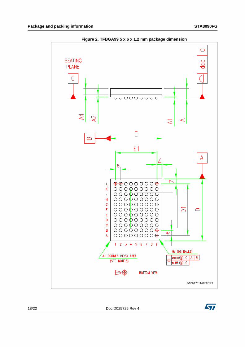
3.2 TFBGA99 5 x 6 x 1.2 mm package information
Table 10. TFBGA99 package dimensions
Symbol Min. Typ. Max
A 1.20
A1 0.15
A2 0.28
A4 0.60
b 0.25 0.30 0.35
D 5.85 6.00 6.15
D1 5.00
E 4.85 5.00 5.15
E1 4.00
e 0.50
F 0.50
ddd 0.08
eee 0.15
fff 0.05
Package and packing information STA8090FG
18/22 DocID025726 Rev 4
Figure 2. TFBGA99 5 x 6 x 1.2 mm package dimension

DocID025726 Rev 4 19/22
STA8090FG Ordering information
21
4 Ordering information
Figure 3. Ordering information scheme
PackingQualified Grade/CAN Bus
TR = Tape and Reel
<blank> = Tray
B = Industrial Grade (with CAN)
<blank> = Industrial Grade (no CAN)
SAL with Stacked Flash
STA8090FG TRB
Example code:
Family identifier

Revision history STA8090FG
20/22 DocID025726 Rev 4
5 Revision history
Table 11. Document revision history
Date Revision Changes
18-Dec-2013 1 Initial release.
09-Apr-2014 2
Updated Features listAdded following chapters:– Chapter 1: Overview
– Chapter 2: Pin description– Chapter 3: Package and packing information– Chapter 4: Ordering information
10-Apr-2014 3
Table 5: Test/emulated dedicated pins:– TRSTn: added note
Table 7: Multimedia card pins:– MMC_CMD: added note
04-Dec-2014 4
Updated Features listTable 1: TFBGA99 connection diagram (with CAN):– K5, K6, K7, K8: updated pin name
Table 2: TFBGA99 connection diagram (no CAN):– K5, K6, K7, K8: updated pin nameTable 3: Power supply pins:
– GND, GND_LNA: updated pin numberTable 4: Main function pins:– ADC_IN2: updated description
– RTC_XTI, RTC_XTO: updated I/O voltageTable 5: Test/emulated dedicated pins:– TDI, TMS: updated description
Table 6: Communication interface pins:– CAN0_RX: added note on CAN0_RX function; updated I/O type
for TSENSE function– CAN0_TX: added note on CAN0_TX function– I2C_CLK, I2C_SD: changed AF3 function
– SPI_CSN: updated I/O type for SQI_CEN function– SPI_DI: updated AF0 description; changed AF1 function– SPI_DO: updated description
– UART0_CTS, UART0_DCD, UART0_DSR: changed AF2 function
– UART0_TX, UART0_RX: changed AF1 I/O type and function
DocID025726 Rev 4 21/22
STA8090FG Revision history
21
04-Dec-20144
(continued)
Table 7: Multimedia card pins:– MMC_CLK, MMC_CMD, MMC_D0, MMC_D1: updated AF1
function– MMC_D2: changed AF1 I/O type and function; updated TSENSE
I/O type;– MMC_D3: changed AF1 I/O type and function
Table 8: General purpose pins:– GPIO1: updated AF0 description; updated AF1 function;
updated TSENSE I/O type– GPIO2: updated AF1 function
Table 11. Document revision history
Date Revision Changes

STA8090FG
22/22 DocID025726 Rev 4
IMPORTANT NOTICE – PLEASE READ CAREFULLY
STMicroelectronics NV and its subsidiaries (“ST”) reserve the right to make changes, corrections, enhancements, modifications, and improvements to ST products and/or to this document at any time without notice. Purchasers should obtain the latest relevant information on ST products before placing orders. ST products are sold pursuant to ST’s terms and conditions of sale in place at the time of order acknowledgement.
Purchasers are solely responsible for the choice, selection, and use of ST products and ST assumes no liability for application assistance or the design of Purchasers’ products.
No license, express or implied, to any intellectual property right is granted by ST herein.
Resale of ST products with provisions different from the information set forth herein shall void any warranty granted by ST for such product.
ST and the ST logo are trademarks of ST. All other product or service names are the property of their respective owners.
Information in this document supersedes and replaces information previously supplied in any prior versions of this document.
© 2014 STMicroelectronics – All rights reserved